
Solar Cell Temperature Dependent Efficiency and Very High ...
304
Purdue University Purdue e-Pubs Open Access Dissertations eses and Dissertations Fall 2013 Solar Cell Temperature Dependent Efficiency and Very High Temperature Efficiency Limits John Robert Wilcox Purdue University Follow this and additional works at: hps://docs.lib.purdue.edu/open_access_dissertations Part of the Electrical and Electronics Commons , Nanoscience and Nanotechnology Commons , and the Oil, Gas, and Energy Commons is document has been made available through Purdue e-Pubs, a service of the Purdue University Libraries. Please contact [email protected] for additional information. Recommended Citation Wilcox, John Robert, "Solar Cell Temperature Dependent Efficiency and Very High Temperature Efficiency Limits" (2013). Open Access Dissertations. 19. hps://docs.lib.purdue.edu/open_access_dissertations/19
-
Upload
khangminh22 -
Category
Documents
-
view
0 -
download
0
Transcript of Solar Cell Temperature Dependent Efficiency and Very High ...

Purdue UniversityPurdue e-Pubs
Open Access Dissertations Theses and Dissertations
Fall 2013
Solar Cell Temperature Dependent Efficiency andVery High Temperature Efficiency LimitsJohn Robert WilcoxPurdue University
Follow this and additional works at: https://docs.lib.purdue.edu/open_access_dissertations
Part of the Electrical and Electronics Commons, Nanoscience and Nanotechnology Commons,and the Oil, Gas, and Energy Commons
This document has been made available through Purdue e-Pubs, a service of the Purdue University Libraries. Please contact [email protected] foradditional information.
Recommended CitationWilcox, John Robert, "Solar Cell Temperature Dependent Efficiency and Very High Temperature Efficiency Limits" (2013). OpenAccess Dissertations. 19.https://docs.lib.purdue.edu/open_access_dissertations/19


SOLAR CELL TEMPERATURE DEPENDENT EFFICIENCY
AND VERY HIGH TEMPERATURE EFFICIENCY LIMITS
A Dissertation
Submitted to the Faculty
of
Purdue University
by
John R. Wilcox
In Partial Fulfillment of the
Requirements for the Degree
of
Doctor of Philosophy
December 2013
Purdue University
West Lafayette, Indiana

ii
To my loving wife Amy T. Wilcox and wonderful family.
Many wonderful educators and friends that have inspired me.
This great country.

iii
ACKNOWLEDGMENTS
I would like to thank Professors Jeffery Gray and Richard Schwartz for their
excellent guidance and instruction. They have been wonderful mentors. I would also like
to thank Professors Mark Lundstrom, Ashraf Alam and Rakesh Agrawal for serving on
my thesis committee, and Dr. Alex Haas, for his collaboration and research. Many
thanks to Dr. Allen Gray, Dr. Myles Steiner, Dr. Mark Osowski, Dr. James
McCambridge and JP Whitlock, their feedback and measurements have been invaluable.
I appreciate the superb learning opportunities available at Purdue University. This work
was supported the by the Very High Efficiency Solar Cell project, Advanced Research
Projects Agency-Energy and Semiconductor Research Corporation through the Network
for Photovoltaic Technology. Facilities and computer resources have been provided by
Purdue’s Birck Nanotechnology Center, Network for Computational Nanotechnology,
Engineering Computer Network and the School of Electrical and Computer Engineering
.

iv
TABLE OF CONTENTS
Page
LIST OF TABLES .............................................................................................................. x
LIST OF FIGURES .......................................................................................................... xii
LIST OF SYMBOLS ..................................................................................................... xxiii
NOMENCLATURE ...................................................................................................... xxxi
ABSTRACT ................................................................................................................. xxxiv
1. INTRODUCTION ........................................................................................................ 1
1.1 The Value of Solar Energy ................................................................................... 1
1.2 Reducing the Cost of Solar Energy ...................................................................... 2
1.2.1 Solar Cell Research .................................................................................. 2
1.2.2 Solar Cell Modeling ................................................................................. 3
1.3 Increasing the Value of Solar Energy ................................................................... 4
1.4 Operating Temperature ......................................................................................... 6
1.5 Dissertation Synopsis ........................................................................................... 7
1.5.1 Detailed Balance Limited Very High Temperature Terminal
Characteristics .......................................................................................... 9
1.5.2 Recombination Limited Very High Temperature Terminal
Characteristics .......................................................................................... 9
1.5.3 Temperature Dependent Resistive Losses .............................................. 10
1.5.4 Temperature Dependent Numerical Model ............................................ 11
2. LITERATURE REVIEW ........................................................................................... 13
2.1 Solar Cell History ............................................................................................... 13
2.2 Solar Cell Fundamentals ..................................................................................... 15
2.3 Modeling Solar Cells .......................................................................................... 16
2.4 Simple Solar Cell Models ................................................................................... 17
2.4.1 Linear Temperature Dependent Curve-fits ............................................. 17

Page
v
2.4.2 Ideal Diode With Resistance .................................................................. 18
2.4.3 Two or More Diode Model ..................................................................... 19
2.4.4 Other Temperature Dependent Solar Cell Models ................................. 19
2.4.5 Summary of Analytical Solar Cell Models ............................................ 20
2.5 Detailed Numerical Models of Semiconductor Devices .................................... 21
2.5.1 Detailed Modeling Programs .................................................................. 21
2.5.2 Temperature Dependent Solar Cell Modeling ........................................ 22
2.5.3 Compare Modeled and Measured Temperature Coefficients ................. 24
2.6 Related Work ...................................................................................................... 24
2.6.1 Simulating the Recombination Limited Terminal Characteristics
at Very High Temperatures .................................................................... 24
2.6.2 Calculating the Series Resistance and Bias Point Losses ....................... 25
2.6.3 Detailed Numerical Modeling Temperature Dependencies ................... 26
2.7 Uncertainty in Temperature Dependent Measurements ..................................... 27
3. DETAILED BALANCE LIMITED VERY HIGH TEMPERATURE
TERMINAL CHARACTERISTICS .......................................................................... 29
3.1 Terminal Characteristics ..................................................................................... 30
3.1.1 Temperature Dependent Terminal Characteristics ................................. 31
3.1.2 Temperature Dependent Terminal J-V Relationship .............................. 33
3.1.3 Bandgap Energy ..................................................................................... 34
3.1.4 Short Circuit Current .............................................................................. 38
3.1.5 Recombination Current Density ............................................................. 44
3.1.6 Open Circuit Voltage .............................................................................. 49
3.1.7 Fill Factor ............................................................................................... 54
3.1.8 Conversion Efficiency ............................................................................ 58
3.2 Real Semiconductor Materials ........................................................................... 63
3.2.1 Extrapolating the Temperature Coefficients .......................................... 63
3.2.2 Finding the Optimal Material ................................................................. 67
3.2.3 Improving the Temperature Coefficients ............................................... 70
3.2.4 3-D effects .............................................................................................. 73
3.3 Summary and Conclusions ................................................................................. 74

Page
vi
3.3.1 Future Work ............................................................................................ 75
4. RECOMBINATION LIMITED VERY HIGH TEMPERATURE
TERMINAL CHARACTERISTICS .......................................................................... 77
4.1 Terminal Characteristics ..................................................................................... 77
4.1.1 Multiple Diode Equation ........................................................................ 78
4.1.2 Recombination Current Density ............................................................. 79
4.1.3 Low-level Injection Limit ....................................................................... 81
4.1.4 High-level Injection Limit ...................................................................... 82
4.1.5 Theoretical Recombination Current Density .......................................... 83
4.2 Semiconductor Material Parameters ................................................................... 86
4.2.1 Intrinsic Carrier Concentration over Bandgap Fit .................................. 87
4.2.2 Recombination Coefficients ................................................................... 92
4.2.3 Shockley Hall Read Recombination ....................................................... 98
4.3 Analytical Simulations ..................................................................................... 102
4.3.1 Bandgap Optimization Over a Range of Temperatures ....................... 102
4.3.2 Conversion Efficiency over Operating Temperature ........................... 108
4.3.3 The Peak Conversion Efficiency and Optimal Bandgap Energy
Over Temperatures and Solar Concentration ....................................... 110
4.3.4 Conversion Efficiency Over Temperature and Solar
Concentration ....................................................................................... 114
4.3.5 The Peak Conversion Efficiency Curve-fit Over Temperatures
and Solar Concentration ....................................................................... 117
4.3.6 Multiple Junctions ................................................................................ 118
4.4 Additional Effects ............................................................................................. 120
4.4.1 Internal Effects ..................................................................................... 121
4.4.2 External and 3-D Effects ...................................................................... 122
4.5 Summary and Conclusions ............................................................................... 123
4.5.1 Future Work .......................................................................................... 124
5. TEMPERATURE DEPENDENT RESISTIVE LOSSES ........................................ 125
5.1 Series Resistance Losses .................................................................................. 130
5.2 Temperature Dependent Non-Ideal Diode Parameters ..................................... 130
5.2.1 Temperature Dependent SC
J ................................................................ 132

Page
vii
5.2.2 Temperature Dependent O
J ................................................................. 133
5.3 Temperature Dependent Resistance ................................................................. 135
5.3.1 Temperature Dependent Lateral Sheet Resistance ............................... 136
5.3.2 Temperature Dependent Metal Resistivity ........................................... 138
5.4 Temperature Dependence of the Equivalent Series Resistance ....................... 139
5.5 Non-unity Ideality Factor and Tandems ........................................................... 143
5.6 Conversion Efficiency Temperature Dependence ............................................ 144
5.7 Summary and Conclusions ............................................................................... 147
6. TEMPERATURE DEPENDENT NUMERICAL MODEL ..................................... 149
6.1 Numerical Modeling ......................................................................................... 150
6.2 The Semiconductor Equations .......................................................................... 155
6.3 Generation Rate ................................................................................................ 157
6.3.1 Obscuration ........................................................................................... 158
6.3.2 Reflectivity ........................................................................................... 161
6.3.3 Photon Absorption ................................................................................ 163
6.3.4 Electrical Bandgap Energy and Electron Affinity ................................ 166
6.3.5 Additional Generation Effects .............................................................. 169
6.4 Recombination Rate ......................................................................................... 170
6.4.1 Radiative Recombination ..................................................................... 171
6.4.2 Single Level Traps ................................................................................ 174
6.4.3 Auger Recombination ........................................................................... 177
6.5 Net Charge ........................................................................................................ 178
6.5.1 Ionized Donor and Acceptor atoms ...................................................... 178
6.5.2 Single Level Trap and Fixed Charges .................................................. 180
6.6 Carrier Mobility ................................................................................................ 180
6.6.1 Theoretical Mobility ............................................................................. 181
6.6.2 Mobility Model ..................................................................................... 182
6.7 Band Parameters ............................................................................................... 185
6.8 Other Parameters .............................................................................................. 186
6.9 Other Temperature Dependent Effects ............................................................. 186

Page
viii
6.9.1 Metal Resistivity ................................................................................... 187
6.9.2 Breakdown Electric Field ..................................................................... 188
6.9.3 Carrier Saturation Velocity ................................................................... 188
6.9.4 Carrier Freeze-Out ................................................................................ 189
6.10 Simulation Results ............................................................................................ 190
6.10.1 Comparison to Measured Devices ........................................................ 192
6.10.2 Analysis of Temperature Coefficients .................................................. 194
6.11 Summary and Conclusions ............................................................................... 198
6.11.1 Future Work .......................................................................................... 199
7. CONCLUSIONS....................................................................................................... 201
7.1 Future Work ...................................................................................................... 203
LIST OF REFERENCES ................................................................................................ 206
A. PHYSICAL CONSTANTS ...................................................................................... 226
B. SIMPLE TEMPERATURE DENPENDENT MODELS ......................................... 227
B.1 Estimating the Short Circuit Current Density .................................................. 227
B.1.1 Temperature Dependent JSC ................................................................. 227
B.1.2 Quantum Efficiency .............................................................................. 228
B.1.3 Optical and Electrical Bandgap Comparison ....................................... 228
B.2 Estimating the Reverse Saturation Current Density ......................................... 231
B.2.1 JO Thermal Effects ................................................................................ 232
B.2.2 JO Curve-Fit Model .............................................................................. 232
C. SIMPLE ANALYTICAL AND NUMERICAL METHODS FOR FINDING
THE TERMINAL CHARACTERISTICS ................................................................ 234
C.1 Analytical Approximations .............................................................................. 235
C.2 Numerical Solutions ......................................................................................... 236
C.2.1 Bisection Approach: N Junctions with 1 Diode in each Junction
and Infinite Shunt Resistance ............................................................... 237
C.2.2 Bisection Approach: M Number of Diodes and Zero Series
Resistance ............................................................................................. 238
C.2.3 Bisection Approach: 1 Junction with M Number of Diodes, with
Finite Series and Shunt Resistances ..................................................... 239

Page
ix
C.2.4 Bisection Approach: N Junctions with Radiative, Auger and SHR
Recombination (Cubic Solution), and Infinite Shunt Resistance ......... 241
C.2.5 Bisection Approach: N Junctions with M Diodes and a Shunt
Resistance in Each Junction, with Series Resistance ........................... 243
C.2.6 Sumary .................................................................................................. 243
D. A METHOD FOR FINDING THE OPTIMAL MULTIPLE JUNCTION
SOLAR CELLS EFFICIENCY ................................................................................ 244
D.1 Example Solution ............................................................................................. 244
D.2 Multi-threaded .................................................................................................. 247
E. PROPERTIES OF J-V CURVES ............................................................................. 248
E.1 Shifting the J-V Curves by the Difference of the VOC ...................................... 248
E.1.1 Case 1: J Away from JSC ...................................................................... 249
E.1.2 Case 2: J Near JSC ................................................................................. 249
E.1.3 Summary ............................................................................................... 250
F. TEMPERATURE DEPENDENT BANDGAP NARROWING ............................... 251
F.1 Common Varshi equation ................................................................................. 251
F.2 Simple polynomial curve-fit ............................................................................. 252
F.3 Bose-Einstein equation ..................................................................................... 253
F.4 Two term Bose-Einstein equation .................................................................... 254
F.5 Two term Bose-Einstein equation with lattice expansion ................................ 255
F.6 Pässler equation ................................................................................................ 255
F.7 Summary ........................................................................................................... 256
G. YEARLY SPECTRAL DATA ................................................................................. 257
G.1 Related Research .............................................................................................. 257
G.2 Measured and Simulated Spectra ..................................................................... 258
G.3 Summary ........................................................................................................... 259
PUBLICATIONS ............................................................................................................ 262
VITA ............................................................................................................................... 267

x
LIST OF TABLES
Table Page
2.1 Detailed numerical model programs commonly used to model solar cells
[71]. ........................................................................................................................23
3.1 Commonly measured terminal characteristics, along with the associated
absolute temperature coefficient and relative temperature coefficients for
each terminal characteristic. ...................................................................................32
5.1 Temperature dependent OJ curve-fit model S’ coefficients (after [104] ©
2011 PSE AG)......................................................................................................134
5.2 Temperature dependent OJ curve-fit model I’ coefficients (after [104] ©
2011 PSE AG)......................................................................................................134
5.3 The intrinsic values for common semiconductors at 300K (after [144]
©2012 IEEE). ......................................................................................................137
5.4 Summary of quasi-3D model parameters. ...........................................................145
6.1 Coefficients for the ,A n and
,A p , Equation (6.36) ............................................183
6.2 Device parameters used in the simulations [96, 201, 202] ..................................191
Appendix Table
A.1 Table of physical constants ..................................................................................226
C.1 Shows under what conditions each of the bisection approaches can be used
numerically finding the FF. .................................................................................237
F.1 Si and GaAs bandgap coefficients for Varshni’s semi-empirical bandgap
equation. ...............................................................................................................252
F.2 Si bandgap coefficients for a polynomial bandgap energy curve-fit. ..................253
F.3 GaAs bandgap coefficients for the Bose-Einstein physics based semi-
empirical bandgap equation. ................................................................................254
F.4 Si bandgap coefficients for O’Donnell’s Bose-Einstein physics based
semi-empirical bandgap equation [172]...............................................................254
F.5 Si and GaAs bandgap coefficients for Pässler’s Bose-Einstein physics
based semi-empirical bandgap equation. .............................................................255

Table Page
xi
F.6 Si and GaAs bandgap coefficients for Pässler’s semi-empirical bandgap
equation. ...............................................................................................................256

xii
LIST OF FIGURES
Figure Page
1.1. Flow diagram showing the inclusion of material parameter dependencies,
with a numerical model. The black arrows show the flow of parameters
from the material parameter framework (MPF) to the semiconductor
equations. The red arrow shows the parameters being passed back to MPF
during the numerical solution process. ..................................................................11
3.1. Example J-V curves of a solar cell at two values of OT . In most solar cells
the SCJ increases as the temperature increases, while the OCV and FF
typically decrease as the temperature decreases. ...................................................31
3.2. Circuit diagram of an intrinsic solar cell................................................................34
3.3. The material specific temperature dependent bandgap narrowing fit for Si
compared to measurements. ...................................................................................35
3.4. The material specific temperature dependent GE narrowing fits for a wide
range of direct and indirect bandgap semiconductor materials [106].
Many of the material specific fit plotted in the figure have been
extrapolated beyond the measured data used to create the fit. ...............................36
3.5. Generic fit for moderate temperature dependent GE narrowing (a), and
high temperature dependent GE narrowing (b). ....................................................38
3.6. Spectral irradiance (a), power available above the simulated GE (b),
fraction of power above the simulated GE (c), and 1-Sun SCJ available
above the simulated GE in the ASTM Standard G173-03 direct spectrum
(AM 1.5 D) (d) [108] .............................................................................................41
3.7. The integrated SCJ available above the simulated GE at 500 Suns. .....................42

Figure Page
xiii
3.8. The the SCdJ
dT and
1 SC
SC
dJ
J dT values for cases with no T dependent GE
narrowing (a) & (b), moderate T dependent GE narrowing (c) & (d) and
high T dependent GE narrowing (e) & (f). The T dependent variation of
the SCJ is relatively small compared to the variation caused by the
absorption gaps in the solar spectrum. ...................................................................43
3.9. The OJ at the simulated GE for 500 Suns. The OJ increases as the OT
increases and the OJ increases exponentially as the GE decreases. .....................45
3.10. The OdJ
dT and
1 O
O
dJ
J dTvalues for cases with no T dependent
GE
narrowing (a) & (b), moderate T dependent GE narrowing (c) & (d) and
high T dependent GE narrowing (e) & (f). The OdJ
dT increases and
1 O
O
dJ
J dT decreases quickly as the GE decreases and the OT increases. ................47
3.11. The OCV at the simulated GE for 500 Suns. As the OT increases the OCV
decreases for a given GE at OT , this is caused by OJ . The OCV increase
nearly linearly as the GE increases. .......................................................................50
3.12. The OCdV
dT and
1 OC
OC
dV
V dT values for cases with no T dependent GE
narrowing (a) & (b), moderate T dependent GE narrowing (c) & (d) and
high T dependent GE narrowing (e) & (f). The OCdV
dT becomes more
negative as the GE increases and as the OT increases. As OT dependent
GE narrowing increases, the dFF
dTbecomes less sensitive to the OT . The
1 dFF
FF dT becomes more negative as the GE decreases, as the OT increases
and as the GE narrowing increases. .......................................................................52
3.13. The FF at the simulated GE for 500 Suns. As the OT increases the FF
decreases for a given GE at OT , this is caused by OJ . ..........................................55

Figure Page
xiv
3.14. The dFF
dT and the
1 dFF
FF dT values for cases with no T dependent GE
narrowing (a) & (b), moderate T dependent GE narrowing (c) & (d) and
high T dependent GE narrowing (e) & (f). Similar to the OCV temperature
coefficients, Figure 3.12, the dFF
dT and the
1 dFF
FF dT both becomes more
negative as the GE decreases, as the OT increases and as the GE
narrowing increases. ..............................................................................................57
3.15. The η at the simulated GE for 500 Suns. As the OT increases the η
decreases for a given GE at OT . In most values of GE as the OT increases
the η decreases. For lower values of GE , the η increases as the GE
increases, this is caused by the increase in the OCV . For higher values of
GE , the η decreases as the GE increases, this is caused by the decrease in
the SCJ . ..................................................................................................................59
3.16. The optimal peak η over OT for a concentration of 500 Suns. As the OT
increases the η decreases. .......................................................................................59
3.17. The d
dT
and
1 d
dT
values for cases with no T dependent GE narrowing
(a) & (b), moderate T dependent GE narrowing (c) & (d) and high T
dependent GE narrowing (e) & (f). The 1 d
dT
is the sum of the
1 SC
SC
dJ
J dT,
1 OC
OC
dV
V dT and
1 dFF
FF dT, this causes the S-Q detailed balance limited
d
dT
and 1 d
dT
to be positive above 2 eV in solar cells with moderate T
dependent GE narrowing and above 1.75 eV in solar cells with high T
dependent GE narrowing. ......................................................................................61

Figure Page
xv
3.18. The black lines are the S-Q detailed balance limit η for each material,
using the T dependent GE narrowing for each of the materials. The red
lines are the linear extrapolated η at 25 °C. The dips in the black line are
caused by the absorption gaps in the solar spectrum. For wide GE
materials such as GaN (a), the S-Q detailed balance limit η can increase
faster than the linear extrapolated η at 25 °C as the OT increases. For
some moderate EG materials such as ZnTe (b), the η can increase as the OT
increases at lower temperatures, due to the T dependence of the SCJ and
then decrease as the OT increases at higher temperatures, due to the T
dependence of the OCV . The lower EG materials, SiC, GaAs, Si and Ge are
plotted in Figure 3.19 .............................................................................................64
3.19. The black lines are the S-Q detailed balance limit η for each material,
using the T dependent GE narrowing for each of the materials. The red
lines are the linear extrapolated η at 25 °C. The dips in the black line are
caused by the absorption gaps in the solar spectrum. For the moderate GE
material SiC (a), the η simulated using the S-Q detailed balance limit and
the linear extrapolated η at 25 °C are almost exactly the same. For GaAs
(b), the S-Q detailed balance limit η decreases faster than the linear
extrapolated η at 25 °C as the OT increases. As was the case with SiC (a),
the Si (c) η simulated using the S-Q detailed balance limit and the linear
extrapolated η at 25 °C are almost exactly the same. For low GE materials
such as Ge (d), the S-Q detailed balance limit η decreases slower than the
linear extrapolated η at 25 °C as the OT increases. The Higher GE
materials, GaN and ZnTe are plotted in Figure 3.19 .............................................65
3.20. The η calculated using the T dependent GE narrowing of real materials,
compared to the optimal peak η calculated in Section 3.1.8. The high GE
material (a) does not reach the optimal peak η, while the moderate GE
materials will reach the optimal peak η. ................................................................68
3.21. The absolute % difference between the η calculated using the T dependent
GE narrowing of real materials and the optimal peak η calculated in
Section 3.1.8. Due to the steps in the GE at the optimal peak η, not all of
the materials reach the optimal peak η. ..................................................................69

Figure Page
xvi
3.22. Compares the case with GE narrowing and the case where the GE is held
constant over OT , for (a) GaN, (b) GaAs, (c) Si and (d) Ge. For wide GE
materials such as GaN, holding the GE constant will decreae the
performance over OT . For moderate GE materials, such as GaAs and Si
there may be a small improvement or a small loss. For narrow GE
materials, such as Ge, holding the GE constant increases the performance
over OT . ..................................................................................................................72
4.1. Multiple diode circuit diagram, with radiative recombination, ,RJ , SHR
recombination, ,R SHRJ , and Auger recombination,
,R AugerJ , as well as series
resistance, SeriesR , and shunt resistance, ShuntR . ......................................................79
4.2. Measured * /nm m and * /pm m for a wide range of direct and indirect
bandgap semiconductor materials [106]. ...............................................................87
4.3. Measured 3/2300inK for a wide range of direct and indirect bandgap
semiconductor materials. Linear curve-fits for direct bandgap and indirect
bandgap materials [106]. The indirect bandgap fit becomes non-physical
below 0.5 eV. .........................................................................................................88
4.4. Measured in for a wide range of direct and indirect bandgap
semiconductor materials [106]. Linear curve-fits of 3/2300inK were used
to predict the in for direct bandgap and indirect bandgap materials. There
is a factor of 10 difference between the in curve-fit for direct bandgap
materials and in curve-fit for indirect bandgap materials .....................................89
4.5. The percentage difference between the measured and the linear curve-fit
predicted values. ....................................................................................................90
4.6. Comparison of the in curve-fits with material specific in values at 300 K.
The lines show the in curve-fits for direct bandgap and indirect bandgap
materials over a range of OT . .................................................................................91
4.7. The red squares are measured B values for direct bandgap materials. The
blue diamonds are measured B values for direct bandgap materials. Low,
medium and high lines have been developed to bracket the B for direct
bandgap and indirect bandgap materials. ...............................................................93

Figure Page
xvii
4.8. The solid black line is the Shockley – Queisser detailed balance limit. The
red dots are the estimated ,OJ for measured solar cells. The blue lines are
the ,OJ predicted by the model for direct bandgap materials. The green
lines are the ,OJ values predicted by the model for indirect bandgap
materials. ................................................................................................................96
4.9. The red squares are the measured C values for direct bandgap materials
and the blue diamonds are the measured C values for indirect bandgap
materials. ................................................................................................................97
4.10. The conversion efficiency predicted by the utlra high temperature model
over simulated bandgap energy for a wide range of selected temperatures.
As the temperature increases the saturation current density increases. This
causes the conversion efficiency to decrease. Also as the temperature
increases the bandgap energy with the highest conversion efficiency for a
given temperature increases. ................................................................................103
4.11. Open circuit voltage predicted by the very high temperatures model over
simulated GE for a wide range of selected temperatures. As the
temperature increases the OCV for the simulated GE decreases. Also, as
the solar concentration increases the OCV increases and the rate of OCV
reduction decreases. .............................................................................................105
4.12. The effective conversion efficiency, '
PV , predicted by the utlra high
temperature model over simulated GE for a wide range of selected
temperatures. This parameter has temperature dependencies that are
similar to the conversion efficiency, however it does not approach zero as
the bandgap energy increases...............................................................................106
4.13. The optimal peak η, ηPV’, f’ and EG plotted for a wide range of selected
temperatures. As the temperature increases the optimal peak η decreases.
In the 2000 suns cases the optimal EG changes very little between 200 °C
and 400 °C. ..........................................................................................................107
4.14. The η simulated for five different recombination cases. At 1 sun the cases
with low and high Auger recombination coefficients and the radiative
recombination equal to the S-Q limit are nearly identical to the S-Q only
limit, which indicates that the Auger recombination is insignificant at this
concentration. At 2000 suns the case with only S-Q and low Auger
recombination are still nearly identical, and the case with a high Auger
recombination coefficient and radiative recombination equal to the S-Q
limit is now reducing the conversion efficiency. This is still small
compared to the cases with low and high radiative recombination, which
are clearly reducing the conversion efficiency more than the Auger
recombination. .....................................................................................................109

Figure Page
xviii
4.15. The optimal efficiency plotted over temperature and solar concentration.
It deceases as the temperature increases and the solar concentration
decreases. .............................................................................................................110
4.16. The optimal EG plotted over temperature and solar concentation. The
steps are caused by the local maxima in Figure 4.10 ...........................................111
4.17. The lines are the conversion efficiency over EG at each of the
temperatures. The local maxima are caused by the gaps in the solar
spectra. The black dots are the peak conversion effiicency and optimal EG
at each of the temperatures. The arrows shows the otpimal EG transitions
between each temperature. As the OT increases from 394 °C to 395 °C
there is a small change in the optimal EG, from 395 °C to 396 °C there is
no change in the optimal EG, and from 396 °C to 397 °C there is a large
change in the optimal EG. These large optimal EG transitions are causing
the steps in Figure 4.16. .......................................................................................112
4.18. (a) The optimal EG for selected concentrations over a range of
temperatures. The steps caused by the solar spectrum can clearly be seen.
(b) The fraction of energy in the spectrum above the optimal EG. ......................113
4.19. (a) is a corner view and (b) is a top-down view of the conversion
efficiency over temperature and bandgap energy at 100 suns
concentration. These plots show how quickly the conversion efficiency
decreases for a given temperature from the optimal EG. The conversion
efficiency decreases as the bandgap increases and as the bandgap
decreases. These plots also show the peak conversion efficiency shifted to
a higher optimal EG as the temperature increases. ...............................................115
4.20. The conversion efficiency over EG relative to the peak conversion
efficiency at each temperature. The four lines through the plot show the
temperature dependent bandgap narrowing of GaAs, CdTe, GaInP with a
25 °C bandgap of 1.6 eV and GaInP with a 25 °C bandgap of 1.8 eV. At
some temperatures, the range of EG with a conversion efficiency less than
5% from the peak is fairly narrow, for other temperatures this range is
considerably wider. The optimal EG clearly increases as the temperature
increases. ..............................................................................................................116
4.21. (a) The lines are the modeled conversion efficiencies over temperature at
each of the concentrations. The dots are estimated using the simple curve-
fit. (b) The absolute error between the results of the model and the curve-
fit. .........................................................................................................................118
4.22. Simulated conversion efficiency over (a) top junction and bottom junction
EG, as well as, (b) bottom junction EG for a two junction three terminal
tandem device operating at 100 suns and 330 °C. The conversion
efficiency peaks are caused by the gaps in the solar spectrum. ...........................119

Figure Page
xix
4.23. The peak conversion for Shockley-Queisser detailed balance limit from 1
to 10 junctions calculated over a range of temperatures. .....................................120
4.24. Melting points for indirect bandgap and direct bandgap materials over the
bandgap range of interest. ....................................................................................122
5.1. (a) Top and (b) corner view of the typical comb shaped grid and busbar
electrodes on the emitter of a generic solar cell. The thick black line is the
busbar and the thin black lines are the grid electodes. The area between
two grid electrodes is a tile and the area between a grid electrode and the
dashed line in (b) is a half-tile. The pink region is the emitter layer and
the light blue region is the absorber layer. The gray arrows and lines
indicate the current flow within the device (after [144] © 2012 IEEE). .............128
5.2. (a) Reverse saturation current density over bandgap for three of the eight
temperatures modeled. (b) Comparison of the pseudo-data OCV over
temperature and the values calculated using the polynomial slope and
intercept OJ (T,EG(300 K)) curve-fit (after [104] © 2011 PSE AG). ..................135
5.3. The temperature dependent LCL SheetR change compared to the LCL SheetR
at 25 °C, for a selected range of the temperature dependent mobility factor,
. As decreases the SheetR above 25 °C increases. For a value of -3,
the SheetR can increase nearly 100% at 100 °C (after [144] ©2012 IEEE). .........138
5.4. The temperature dependent change of the metal resistivity, M , compared
to M at 25 °C, for a selected range of the temperature dependent metal
resistivity coefficient, . As increases, the M above 25 °C
increases. For an value of 0.008 K-1
, the M can increase nearly 60%
at 100 °C (after [144] ©2012 IEEE). ...................................................................139
5.5. The simulated eqR for SheetR = 100 Ω/ (a), (c) and (e), also for SheetR =
500 Ω/ (b), (d) and (f). The dashed line is the analytical solution at
25 °C. The solid lines were simulated using the quasi-3D distributred
emitter model. These lines are closer together in (a) and (b), where γ = -0.5
and further apart in (e) and (f), where γ = -2.5. The difference between the
dashed black line and the solid black line is caused by the bias-point loss,
which is higher when the SheetR is higher (after [144] ©2012 IEEE). .................141

Figure Page
xx
5.6. Plots of the eqR simulated over Tw for a range of n, for SCJ = 1,500
mA/cm2, OT = 100 °C and = -2.5. (a) is for a SheetR value of 100 Ω/
and (b) is for a SheetR value of 500 Ω/. The quasi-3D simulated eqR
approaches the analytical approximation of eqR at 100°C as the n of the
solar cell increase (after [144] ©2012 IEEE).......................................................144
5.7. The simulated η over a range of grid electrodes at 25 °C and 100 °C. The
difference between the 25 °C and 100 °C η is caused by the temperature
dependence of the LR . The red square shows the optimal GN for the peak
efficiency at 25 °C. The green triangle shows the corresponding η at
100 °C for the optimal GN at 25 °C. The light blue asterisk shows the
optimal GN for the peak efficiency at 100 °C. The pink star shows the
corresponding η at 25 °C for the optimal GN at 100 °C (after [144] ©2012
IEEE)....................................................................................................................146
5.8. The η temperature coefficient over γ for LR = 0 Ω/, shown in solid black,
and LR = 500 Ω/, shown by blue line with circles. The value of γ has no
affect in the LR = 0 Ω/ case. The temperature coefficient becomes worse
as the as the γ value becomes more negative (after [144] ©2012 IEEE). ............147
6.1. Physical material parameters used in the semiconductor equations, Section
6.2. Each of these material parameters will be discussed in Section 6.3
through Section 6.8. .............................................................................................152
6.2. The substituent T dependent material parameter dependencies, are needed
to solve the semiconductor equations. These parameters will be discussed
in the following subsections.................................................................................153
6.3. Doping dependent material parameters. The real and imaginary
components of the dielectric constant are doping dependent. The bandgap,
electron affinity, effective masses and ionized dopants will also vary with
material doping. ...................................................................................................154
6.4. Minority free carrier concentration dependent material parameters, beyond
the common dependencies. The bandgap, and effective masses will vary
with material doping. ...........................................................................................154
6.5. Electric field dependent material parameters. The electric field affects the
imaginary component of the dielectric constant, the break down voltage,
bandgap, electron affinity, effective masses and dopant ionization
energies. ...............................................................................................................155
6.6. Diagram of a basic solar cell. Busbars and grid lines are added to solar
cell to reduce the resistivity. Texturing [37] (not shown in figure) and
ARCs are added to the top of the solar cells to reduce the reflectivity. ...............159

Figure Page
xxi
6.7. Si bandgap energy over a wide range of temperatures (left) and near the
operating temperature range of interest [98, 99, 103, 168, 172, 173]. Fits
are plotted over their recommended temperature ranges. The red and
black lines are almost identical over the temperature range of interest. ..............167
6.8. (a) Comparison of measured and modeled n over T for a range of DN
[146]. (b) Comparison of measured and modeled pn over DN at 300 K. ........184
6.9. Comparison of measured and modeled n +p over a range of the np
product values. .....................................................................................................185
6.10. The dependent drift velocity, dv , for Si at three different temperatures
[63]. The carrier saturation velocity, satv , decrease as the T increases. .............189
6.11. The terminal characteristics predicted by a single detailed numerical
model over a range of OT , solid line. Each of the terminal characteristics
are relatively close to the measured device characteristics, diamonds. (a)
The SCJ is slightly higher than the measured characteristics near 25 °C.
The (b) OCV and (c) FF are essentitally the same as the measured data near
25 °C. The OT dependent terminal characteristics are shown in Figure
6.12.......................................................................................................................193
6.12. The temperature dependent terminal characteristics at 25 °C predicted by
the detailed numerical model ploted versus the associated terminal
characteristics at 25 °C, red dots, compared to the measured device
characteristics, diamonds. The terminal characterics range is ± 1% of the
measured characteristics. (a) The simulated SCJ is 0.9% higher than the
measured characteristics and the 1 SC
SC
dJ
J dT is 1/3 of the measured OT
dependent terminal characteristics. The terminal characteristics and OT
dependent terminal characteristics of OCV (b) and FF (c) are essentitally
the same as the measured data. The simulated OCV causes the modeled η
to be slightly smaller than the measured value. The difference between
the simluated and the measured 1 d
dT
is caused by the
1 SC
SC
dJ
J dT. ....................196

Figure Page
xxii
Appendix Figure
B.1. (a) GaInAs EQE measured at a range of temperatures. Both the low and
high energy portions of the EQE are temperature dependent. (b)
Comparison of the GaInAs JSC(TO) calculated using EQE measured at
three temperatures, with the 25º C EQE shifted over a range of operating
temperatures (after [117] © 2011 IEEE). ............................................................228
B.2. Varshni bandgap coefficients for a wide variety of semiconductor
materials. (after [117] © 2011 IEEE). ................................................................229
B.3. Bandgap energy temperature dependence for a wide variety of
semiconductor materials in Figure B.2. ...............................................................230
B.4. (a) Calculated electrical ΔEG(TO) for the GaInP, GaInAs and Ge bandgaps
in this tandem solar cell, and measured EQE optical ΔEG(TO) for GaInAs
and GaInP. (b) GaInAs EQE shifted by GaInAs electrical ΔEG(TO) to 25º
C (after [117] © 2011 IEEE)................................................................................231
D.1. The 2 junctions peak system conversion efficiency and the corresponding
2-D system conversion efficiencies plotted for all possible top junction
and bottom junction combinations. ......................................................................245
D.2. The 3 junctions peak system conversion efficiency and the corresponding
2-D system conversion efficiencies plotted for all possible top junction
and bottom junction combinations. ......................................................................246
D.3. The 10 junctions peak system conversion efficiency and the corresponding
2-D system conversion efficiencies plotted for all possible top junction
and bottom junction combinations. ......................................................................246
E.1. The blue curve shows the J-V curve with the JO,1=1x10-29
mA/cm2. The
red curve shows the J-V curve with the JO,2=1x10⁻⁶
mA/cm2. The red dot-
dash line shows the JO,1 curve shifted by the difference of VOC,1 and VOC,2,
which matches the JO,2 curve. The max power point changes as the VOC
changes. ................................................................................................................250
G.1. Direct Normal Incidence (DNI) spectral irradiance data, every ten minutes
throughout each day, for every day of the year, data collected by the report
author. ..................................................................................................................258
G.2. DNI data measured at NREL in Golden, CO [25], data collected by the
author. ..................................................................................................................259

xxiii
LIST OF SYMBOLS
BA Area of the busbars [cm2]
MA Metal conductor cross-sectional area [cm2]
TA Total area of the solar cell surface [cm2]
B Radiative recombination coefficient [cm3/s]
c Speed of light [cm/s]
C Total Auger recombination coefficient [cm6/s]
nC Auger recombination coefficients for electrons [cm6/s]
pC Auger recombination coefficients for holes [cm6/s]
D Diffusion coefficient [cm2/s]
0E Vacuum energy level [eV]
CE Conduction band energy [eV]
DE Energy level of the donor states [eV]
GE Bandgap energy [eV]
(0)GE Bandgap at zero degrees K [eV]
iE Intrinsic Fermi energy [eV]
VE Valance band energy [eV]
totE Total energy incident on the solar cell [W/cm2/s]
E Photons energy [eV]
nF Quasi Fermi energy for electrons [eV]
pF Quasi Fermi energy for holes [eV]
FF Fill factor

xxiv
G Generation rate [cm-3
s-1
]
Ag Acceptor impurity level degeneracy factor
Dg Donor impurity level degeneracy factor
h Planck’s constant [eV s]
J Terminal current density [mA/cm2]
dispJ
Displacement current density [mA/cm2]
MPJ Maximum power circuit density [mA/cm2]
nJ Electron current density [mA/cm2]
OJ Reverse saturation current density [mA/cm2]
pJ Hole current density [mA/cm2]
RJ Recombination current density [mA/cm2]
,R AugerJ Auger recombination current density [mA/cm2]
,R RadJ Radiative recombination current density [mA/cm2]
,R SHRJ Shockley-Read-Hall recombination current density [mA/cm2]
SCJ Short circuit density [mA/cm2]
k Boltzmann constant [eV/K]
ek Imaginary portion of the refractive index
Gl Grid line length [cm]
Bl Busbar length [cm]
Ml Metal conductor length [cm]
DL Diffusion length [cm]
*m Effective mass [kg]
*
cm Conductivity effective mass [kg]
*
,c nm Conductivity effective mass for electrons [kg]
*
,c pm Conductivity effective mass for holes [kg]

xxv
*
dm Density of states effective mass [kg]
*
,d cm Density of states effective mass for electrons in the conduction band [kg]
*
,d vm Density of states effective mass for holes in the valence band [kg]
*
hhm Effective mass of holes in the heavy hole band [kg]
*
lm Longitudinal effective mass [kg]
*
lhm Effective mass of holes in the light hole band [kg]
*
som Effective mass of holes in the split off band [kg]
*
tm Transverse effective mass [kg]
*
thm Thermal velocity effective mass [kg]
*
,th nm Thermal velocity effective mass for electrons [kg]
*
,th pm Thermal velocity effective mass for holes [kg]
om Mass of a free electron [kg]
n Electron concentration [1/cm3]
n
Complex refractive index
Augern Auger recombination ideality factor
in Intrinsic carrier concentration [cm-3
]
mn Ideality factor
on Equilibrium electron concentration [cm-3
]
rn
Real portion of the refractive index
Radn Radiative recombination ideality factor
SHRn Shockley-Read-Hall recombination ideality factor
Tn Filled SHR trap states
N Net bound charge [cm-3
]
AN Acceptors doping concentration [cm-3
]
AN- Ionized acceptor doping concentration [cm
-3]

xxvi
BN Ionized doping concentration [cm-3
]
CN Effective density of conduction band states [cm-3
]
DN Donor doping concentration [cm-3
]
DN+ Ionized donor doping concentration [cm
-3]
GN Number of grid lines
itN Fixed interface charges [cm-3
]
NOCT Nominal operating cell temperature [K]
otherN Other charges [cm-3
]
SN Fixed surface charges [cm-3
]
,ST nN Surface density of trap states for electrons [cm-2
]
,ST pN Surface density of trap states for holes [cm-2
]
SLTN Concentration of charge in SLT recombination sites [cm-3
]
TN Density of traps [cm-3
]
VN Effective density of valence band states [cm-3
]
p Hole concentration [cm-3
]
op Equilibrium hole concentration [cm-3
]
Tp Empty SHR trap states [cm-3
]
P Polarization [C/cm2]
PIn Input power [mW/cm2]
PMax Maximum output power [mW/cm2]
q Electric charge [C]
( )R Wavelength dependent reflectance
AugerR Auger recombination rate [cm-3
s-1
]
BR Busbar resistance [Ω/cm2]
CR Grid electrode-emitter contact resistance [Ω/cm2]
eqR Equivalent resistance [Ω-cm]

xxvii
LR Resistance of the top lateral conducting layers [Ω/cm2]
GR Grid electrode resistance [Ω/cm2]
IR Interface traps recombination rate [cm-3
s-1
]
MR Metal conductor resistance [Ω]
nR Electron recombination rate [cm-3
s-1
]
otherR Recombination rate of other types of recombination [cm-3
s-1
]
pR Hole recombination rate [cm-3
s-1
]
RR Resistance of the back lateral conducting layers [Ω/cm2]
SR Surface recombination rate [cm-3
s-1
]
SeriesR Series resistance [Ω/cm2]
SheetR Sheet resistance [Ω/]
SHRR Shockley-Read-Hall recombination rate [cm-3
s-1
]
ShuntR Shunt resistance [Ω/cm2]
SLTR Single layer traps recombination rate [cm-3
s-1
]
TR Total recombination rate [cm-3
s-1
]
R Radiative recombination rate [cm-3
s-1
]
S Optical obscuration
BS Busbar obscuration
GS Grid line obscuration
nS Surface recombination coefficients for electrons [cm/s]
otherS Any other structure causing obscuration
pS Surface recombination coefficients for holes [cm/s]
t Time [sec]
Et Emitter layer thickness [cm]
Gt Gird electrode thickness [cm]

xxviii
Bt Busbar electrode thickness [cm]
At Absorber layer thickness [cm]
T Operating temperature [K]
aT Ambient air temperature [K]
fT Final temperature [K]
iT Initial temperature [K]
MT Characterization temperature [K]
NT Normalized operating temperature [K]
OT Operating temperature [K]
T Transmission of light through a material
thv Thermal velocity [cm/s]
windv Wind speed [cm/s]
V Terminal voltage [V]
V ' Node voltage [V]
MPV Maximum power voltage [V]
OCV Open circuit voltage [V]
w Solar cell thickness [cm]
Bw Width of the busbar [cm]
Gw Width of the grid lines [cm]
Tw Width of a tile [cm]
x Position inside the solar cell [cm]
X Solar concentration [suns]
Wavelength dependent absorption coefficient [cm-1
]
L Linear thermal expansion coefficient [K-1
]
E Optical or electrical bandgap change [eV]
GE Temperature dependent bandgap change [eV]

xxix
,G CE Minority free carrier concentration dependent bandgap narrowing [eV]
, G DE Doping dependent bandgap narrowing [eV]
, G F KE Franz-Keldysh stark effect bandgap narrrowing [eV]
, G SE Stark effect bandgap narrowing [eV]
SE Split off band energy difference [eV]
n Excess electron concentration [1/cm3]
p Excess hole concentration [1/cm3]
T Temperature difference between aT and T [K]
Δw Change in metal width [cm]
Electric field [V/cm]
br Breakdown electric field [V/cm]
0 Permittivity in a vacuum [F/cm]
r Relative permittivity
s Dielectric constant [F/cm]
(0)S Dielectric constant at zero K [F/cm]
Solar cell conversion efficiency [%]
'
PV Effective conversion efficiency [%]
Wavelength [nm]
G Semiconductor bandgap wavelength [nm]
0 Wavelength of photon in a vacuum [nm]
ii Ionized impurity scattering [cm2/Vs]
L Acoustic phonon scattering mobility [cm2/Vs]
o Magnetic permeability in a vacuum [H/cm]
n Electron mobility [cm2/Vs]
p Hole mobility [cm2/Vs]

xxx
POP Polar-optical-phonon scattering mobility [cm2/Vs]
r Relative magnetic permeability
Wave propagation velocity [cm/s]
M Metal resistivity [Ω cm]
S Emitter layer resistvity [Ω cm]
,S n Capture cross sections for electrons [cm2]
,S p Capture cross section for holes [cm2]
n Electron SHR recombination lifetime [s]
p Hole SHR recombination lifetime [s]
Auger Auger recombination effective lifetime [s]
Eff Effective lifetime [s]
Rad Radiative recombination effective lifetime [s]
SHR SHR recombination lifetime [s]
Electrostatic potential [V]
n Valance band parameter [V]
p Conduction band parameter [V]
( )i Wavelength dependent photon flux density [W/cm2]
Photon flux density incident on the front surface of the solar cells
Electron affinity [V]

xxxi
NOMENCLATURE
1-D One-dimensional
1-Sun Unconcentrated solar irradiance
2-D Two-dimensional
3-D Three-dimensional
a-Si Amorphous Silicon
ADEPT A device emulation program and toolbox
AM 0 Solar spectrum above the atmosphere
AM 1.5 D Standard DNI solar spectrum
AM 1.5 G Standard global solar spectrum
ARC Anti-reflectance coatings
ASTM American Society for Testing and Materials
AZO Aluminum zinc oxide
BSF Back surface field
c-Si Crystalline silicon
C-V Capacitance-voltage measurement
CCD Charge-coupled device
CIGS Copper indium gallium selenide
CMOS Complementary-symmetry metal–oxide–semiconductor
CO2 Carbon dioxide
CPV Concentrator photovoltaic
CPV-T Hybrid CPV and thermal CSP system
CSP Concentrated solar power
DNI Direct normal incidence
Dark I-V Current-voltage sweep in the dark

xxxii
EQE External quantum efficiency
FELES Finite element light emitter simulator
GaAs Gallium Arsenide
GaInAs Gallium Indium Arsenide
GaInP Gallium Indium Phosphide
GaN Gallium Nitride
GaP Gallium Phosphide
Ge Germanium
HIT Heterojunction with intrinsic thin layer
IMM Inverted metamorphic
III-V Semiconductors with a group 13 element(s) and a group 15 element(s)
ITO Indium tin oxide
IQE Internal quantum efficiency
Laser Light amplification by stimulated emission of radiation
LCL Lateral conducting layers
LED Light-emitting diode
Light I-V Illuminated current-voltage sweep
MODTRAN Moderate resolution atmospheric transmission
MOSFET Metal oxide semiconductor field effect transistor
MPF Material parameter framework
NREL National Renewable Lab
PL Photoluminescence spectroscopy
Quasi-2D 1-D simulation of 1-D elements
Quasi-3D 2-D simulation of 1-D elements
S-Q Shockley-Quisser detailed balance limit
SMARTS Simple model of the atmospheric radiative transfer of sunshine
Si Silicon
SiC Silicon Carbide
SiO2 Silicon dioxide
SHR Shockley -Hall-Read

xxxiii
SLT Single layer traps
SRRL Solar Radiation Research Laboratory at NREL
TCL Transparent conducting layers

xxxiv
ABSTRACT
Wilcox, John R., Purdue University, Ph.D., Purdue University, December 2013. Solar
Cell Temperature Dependent Efficiency and Very High Temperature Efficiency Limits.
Major Professor: Jeffery Gray.
Clean renewable solar energy is and will continue to be a critically important source
of electrical energy. Solar energy has the potential of meeting all of the world’s energy
needs, and has seen substantial growth in recent years. Solar cells can convert sun light
directly into electrical energy, and much progress has been made in making them less
expensive and more efficient. Solar cells are often characterized and modeled at 25 °C,
which is significantly lower than their peak operating temperature. In some thermal
concentrating systems, solar cells operate above 300 °C. Since increasing the
temperature drastically affects the terminal characteristics, it is important to quantify the
losses caused by raising the temperature. Methodologies for including the temperature
dependent material parameters in analytical and detailed numerical models have been
examined. The analytical model has been developed to analyze Shockley-Queisser
detailed balance limit, as well as the Auger, Radiative and SHR recombination limiting
cases from 25 °C to 800 °C, at 1x, 500x and 2000x suns concentrations. The results of
this analysis show that the efficiency of a direct bandgap material with an optimal
bandgap could reach 19 % at 400 °C and 2000x suns, if the SHR recombination is
reduced to an acceptable level. An analytical solar cell model was also used in a quasi-
3D numerical model to simulate the temperature dependent resistivity losses. It was
found that the resistive losses can double when the temperature of a solar cell increases
from 25 °C to 100 °C. This will cause the conversion efficiency temperature coefficient
to deteriorate by 10%. By using the temperature dependent material parameters for Si in

xxxv
a detailed numerical model, it was found that some of the adjustable parameters, such as
the base thickness, increase the conversion efficiency temperature coefficient and the
VOC, while other parameters would only increase the VOC. This conclusion can be used
by solar cell manufactures to improve the solar cell parameters with the biggest possible
gain in device performance.

1
1. INTRODUCTION
1.1 The Value of Solar Energy
Interest in renewable energy has surged in recent years, as the world strives to reduce
its dependence on fossil fuels, while at the same time reducing the greenhouse gas
emissions and pollutions. The usages of all forms of renewable energy have increased
over the past few years. Some types of renewable energies, such as hydropower and corn
based ethanol, have reached limits in what is currently technically feasible. Other forms,
such as wind and solar energy, have experienced enormous growth over the past 5 years
[1]. Wind increased 27.6% and solar has increased 69% from 2000 to 2009 [2]. Solar
cell installation has experienced a 130% year-on-year growth from 2009 to 2010 [2, 3].
Solar energy is one form of renewable energy that has the potential to provide all of the
world’s current energy usage. More energy reaches the earth’s atmosphere in one hour,
174,000 [TWh] [4], than all forms of primary energy used worldwide in the last reported
year (2008) which was a total of 144,453 [TWh] [5], (similar to analysis by [6]).
Many +200 MW utility sized power plants are being installed around the world [7,
8]. In 2010, 17 GW of solar cells were installed globally [2]. Solar cells are a reliable
energy conversion device, which can have warranties of up to 25 years [9]. Most solar
cells are a safe and clean way to produce electricity; they can also be recycled to reduce
waste. While generating electrical power, solar cells do not require a fuel source, other
than the sun, and do not produce emissions of any kind. Typically, solar cells only use a
limited amount of water, which is used primarily to wash the solar cell modules [10]. In
comparison, a coal power plant produces 36 times more CO2 and uses 41 times more
water. Electricity generated from a solar thermal system uses over 100 times more water
than solar cells; and hydroelectric losses are 200 times more than solar due to the
evaporation from the reservoir.

2
Clearly there are many advantages to generating more electrical energy using solar
cells. Two of the primary limitations of the future growth of solar energy are the
installation cost and the cost of the available storage options, to store the energy for later
use. Methods for reducing the cost of solar cells will be discussed in Section 1.2.
Approaches to increase the value of solar energy will be discussed in Section 1.3.
1.2 Reducing the Cost of Solar Energy
The solar cell industry has experienced double digit year over year growth for the
past 10 years [11]. The growth in the solar industry has been fueled by decreasing
production costs, which are currently below $0.75/watt [12], as well as government
incentives and feed in tariffs. At the same time, significant improvements have been
made in cell and module efficiencies of each type of solar cell material [13].
The cost of electric energy is often reported as a Levelized Cost of Electricity
(LCOE). LCOE is a common metric used to compare the cost of generating electricity.
It includes the cost to build the power plant, financing, maintenance and fuel. Until very
recently, the LCOE of solar cells has been much higher than many other types of
electrical energy generation on the grid.
A significant amount of money and resources are being devoted to reduce the cost of
installing a solar cell system. In 2011, the U.S. Department of Energy launched the
SunShot Initiative, which aims to reduce the installed cost of solar energy 75%, to $0.05
per kilowatt-hour and $1 per watt by 2020 [14]. This ambitious goal is ontrack to occur
if the cost of solar cell systems continues to decrease at the same rate it has for the past
10 years. This will make solar energy cost competitive with other forms of electricity on
the grid.
1.2.1 Solar Cell Research
There are a variety of ways in which the LCOE of solar energy can and is being
reduced even further. Research is currently under way on a wide variety of solar cell
materials and systems in an ongoing effort to reduce the LCOE in the following ways:

3
1. Reduce the manufacturing and production costs.
2. Increase the efficiency of existing solar cell systems and technologies.
3. Use low cost substrates and materials, such as thin films and organic materials.
4. Use concentrators to reduce the amount of solar cell material needed.
5. Reduce the cost of the balance of system components, such as mounting hardware
and inverters.
6. Decrease the efficiency temperature coefficients of existing technology
In addition to reducing the LCOE of an installed solar electricity generation, research
is also being conducted to improve the way in which solar energy is connected and used
on the electricity gird. One method to more easily incorporate renewable energy on the
grid, is through the use of load balancing. Another method would be to create a smarter
electrical grid that can react quickly to changes in the electrical generation.
The work presented in this report uses measured data and solar cell modeling to
identifying ways in which the value of solar energy can be increased. Possible methods
to increase the value of solar energy, such as focusing on increasing the conversion
efficiency or reducing the conversion efficiency temperature coefficient will be
examined.
1.2.2 Solar Cell Modeling
In order to improve the efficiency of solar cells, it is important to identify the loss
mechanisms reducing the efficiency. A variety of solar cell models have been developed
to better understand the internal physical operation. These range from simple analytical
expressions, to analytical models, to advanced detailed numerical models. Well-
developed models allow the solar cell loss mechanisms to be quantified, enabling
researchers to identify ways to reduce these losses. The models also allow parameter
sensitivities to be located, which then can be used to direct tolerances during
manufacturing processes. Reliable models can also be used to estimate the available
improvements to be gained from redesigning the solar cell. In addition, detailed
numerical models allow the internal operation to be analyzed, which can be difficult or

4
near impossible to accurately measure. Thus solar cell models can speed up development
time and reduce the number of experimental devices needed by testing a variety of
possibilities quickly.
1.3 Increasing the Value of Solar Energy
Presently there is a significant amount of interest in increasing the value of solar
energy through lowering the installaed cost, as well as improving both the quality and
flexibility of the power generated. Recently a 2 day workshop was conducted by ARPA-
E which was focsed on identifying possible new ways of increasing the the overall value
and usefulness of solar [15]. This is a particularly important topic because as the price of
solar energy produced by solar cells has decreased and approached the cost of other
forms of electricity generation it has become a far more competitive and viable energy
option. The cost of electricity produced by solar cells has continued to decrease for many
years. This is being aided by research efforts such as the DOE SunShot Initiative. While
it is likely that the price of installed solar will increase in the near term, as demand
catches up with the over supply, the price will likely continue to decrease as solar cells
become more of a commodity. The rising amount of installed solar power is causing
problems in the electrical grid. This is also causing problems when costumers are paid
full retail rate for the power they produce, leading to fewer users paying for the power
grid mantainance. This could further destabilize the electrical grid. It is therefore
important to identify ways in which solar energy can limit these affects.
There are four ways in which this can be done: improve consistency, dispatchability,
portability and long term storability of solar energy. Improving consistency of solar
energy makes it more valuable to electric grid operators, because they will need less
backup generation capacity. Increasing the dispatchability means being able to store the
solar energy until the grid needs it. Converting the solar energy into a dense fuel source
would increase the portability allowing it to be used as a transportation fuel or used as an
energy source at remote locations. Using a transportation fuel derived from solar energy
would reduce the amount of other transportation fuels used, such as petroleum. Long-
term storage is the ability to store the energy derived from solar for days, weeks, or

5
months, before it is used. This is particularly useful since the energy can be stored when
solar energy is most abundant and used whenever the storage energy is most valuable.
Solar cells are a useful way of harnessing solar energy. They can very efficiently
convert photons directly into electrical energy. Since energy is lost in each energy
conversion, this simple direct conversion of photons to electricity leads to the high
conversion efficiency. This also leads to an important limitation of solar cells. Once
electricity is generated it must be used or stored immediately. Conventional methods of
storaging electricity such as batteries, pumped storage and fly wheels in large scale are
currently prohibitively expensive. Because solar cell technologies available today
convert photons directly into electrical energy, there are no intermediate steps where
storage could be conveniently added. This limits the consistency and dispatchability of
solar energy from solar cells.
Concentrated solar power (CSP) is another solar energy technology which converts
photons into thermal energy and then converts the thermal energy into electricity. Since
the thermal energy can be easily stored, it can be more consistent and dispatchable than
solar cells. A variety of CSP systems are currently being built and tested. These systems
include heliostats towers, parabolic troughs and parabolic dishes. Large scale utility CSP
systems are currently in use throughout the world. Due to the decreasing price of solar
cells, CSP systems recently have become more expensive than flat plate solar cell
systems. They are also limited by the water usage, which is often scarce in high solar
insolation areas. Using the inherent advantages of each, it could be possible to build a
hybrid system that overcomes the limitations of each technology.
It may be possible to increase the value of solar energy by creating a system that
collects both electrical energy using solar cells and thermal energy using a thermal
absorber [15]. Such a system could potentially convert more energy per square meter
into usable energy. This type of combined photovoltaic and thermal system has been
analyzed by Luque [16]. The availability of electrical and thermal energy also makes it
possible to use a variety of storage methods, which could harness both forms of energy,
increasing the value. This includes battery systems that are heated thermally to reduce
the amount of energy needed to charge them electrically. Another approach would be to

6
use the common molten salt method of the thermal storage and use a pumped heat
electrical storage system to store the electricity as thermal energy until it is needed [17,
18]. It may also be possible to directly combine the thermal storage and pumped heat
system to create an even better hybrid system.
1.4 Operating Temperature
While an extensive amount of research has been conducted measuring and modeling
solar cells near the standard test conditions, 25° C, a much smaller amount of research
has been conducted measuring and modeling solar cells at other temperatures, T, and over
the expected operating temperature, OT , range. Solar cells installed in most locations will
operate above and below the standard test conditions. The OT is set by the ambient air
temperature, aT , plus the difference between the aT and the solar cell junction
temperature, T .
O aT T T (1.1)
At moderate latitudes terrestrial flat panel Si solar cells can operate between -10 °C
and 60 °C , and solar cells inside of concentrator photovoltaics (CPV) systems can reach
temperatures as high as 100 °C [19]. Solar cells used on space satellites typically operate
between 50 °C to 80 °C, and in one system are being designed to operate up to 350 °C
[20], for missions into the outer corona of the Sun [21]. The solar cells used on probes to
the outer planets of the solar system operate at much lower temperatures. Cryogenic
systems have been used to measure solar cells down to -173 °C (100 K) [22]. Hybrid
CPV and thermal CSP (CPV-T) systems are being considered that could operate up to
400 °C or higher [23, 24]. Published solar cell performance has been measured over
350 °C [23]. This is important because the conversion efficiency of most crystalline solar
cells decreases as the OT increases.
The temperature of a solar cell while it is operating depends on many parameters,
such as the total energy incident on the solar cell, totE , the air temperature (ambient), aT ,
the nominal operating cell temperature, NOCT, and the wind speed, windv . The

7
parameters totE , aT , and
windv have been measured [25] and modeled for a typical
metrological year [26], throughout each day and year, for a wide variety of locations in
the United States. Because of thermal resistance between the solar cell and air, there will
be a temperature difference between aT and T, equation (1.1).
When wind speed is not accounted for, the operating temperature equation used by
Emery is [27]
2( 20 ) / 800[ / ] totT NOCT C E W m
(1.2)
Methods for calculating T including wind speed have also been derived [28]. This
will allow the T of the solar cell to be calculated throughout each day for every day of
the year. The OT can then be used to model the performance of the solar cell over the
each day of the year.
1.5 Dissertation Synopsis
The focus of this work is analyzing the temperature dependencies of solar cells, as
well as identifying possible ways in which solar cells can be redesigned to reduce the
temperature dependent losses. This is particularly important for solar cell systems where
the OT will vary over a wide range of temperatures and when operating solar cells at very
high temperatures. This work is dividing into three main topics: very high temperatures
(Chapter 3 and Chapter 4), 3-D resistive losses (Chapter 5) and detailed numerical
modeling of Si solar cells (Chapter 6). Chapter 2 reviews the related published literature.
Chapter 7 summarizes the completed work and discusses possible future work. The
appendices provide additional information about models used in this work. These
chapters will support a number of interesting and unexpected conclusions:
Conclusion #1: Improving the OCV will not always yield a better 1 d
dT
Many groups have noticed that as the OCV increases the 1 OC
OC
dV
V dT improves. While
it might be easy to think that this is always true, it may not be true in every case.

8
Improving the OCV leads to an improved and a better 1 OC
OC
dV
V dT will lead to an
improved 1 d
dT
. However, it is easy to over look how changing the OCV will affect the
SCJ and FF , which will also affect the 1 d
dT
.
Conclusion #2: A solar cell with the highest may not have the best 1 d
dT
This related to conclusion 1. There are conditions where improving the at one OT
will cause the 1 d
dT
to become worse. This will lead to lower at higher OT .
Conclusion #3: A solar cell with the highest or with the best 1 d
dT
may not
yield the best performance over a range of temperature
Because of conclusion #3 optimizing for a solar cell with the highest possible or
the best possible 1 d
dT
at one temperature can lead to a device with a lower performance
over a range of OT .
Conclusion #4: Need to optimize for the best yearly performance
While research groups continue to work to achieve the highest possible conversion
efficiency at 25 °C. Because of conclusions #1, #2 and #3, the best solar cell design can
be achieved by optimizing for the optimal yearly performance. There are a number of
yearly performance metrics by which the solar cell designs could be judged.
Possible optimization metrics:
o Highest kWh out per year
o Lowest LCOE
o Higher energy during a particular season
Need more energy during the Summer
More efficient during the Winter
o Most beneficial for the power grid
Reduce the peak load

9
Broad over the entire day
o Longest system lifetime
Conclusion #5: A detailed numerical model can be used to understand the
operating condition dependencies
While the MPF model developed and presented in this work has some limitations, it
shows that it is possible to simulate the dependencies over a wide range of OT . It also
shows that the material parameter dependencies can be measured and modeled. The
results of this model can be used to identify the missing material parameter dependencies.
Each of these conclusions will be discussed further in Chapter 3 through Chapter 6.
While each of these effects might not be large in every situation, it is important to
understand how they will affect the overall performance.
1.5.1 Detailed Balance Limited Very High Temperature Terminal Characteristics
Chapter 3 explorers the Shockley-Queisser (S-Q) detailed balance limited terminal
characteristics and the temperature dependent terminal characteristics over a wide range
of OT , from 100 °C to 800 °C. These calculations are similar to calculations by other
groups. The temperature dependent affects of each of the terminal characteristics and the
temperature dependent terminal characteristics will be evaluated and compared. The
results in this chapter will be helpful in understanding the temperature dependent affects
in later chapters.
1.5.2 Recombination Limited Very High Temperature Terminal Characteristics
Chapter 4 estimates the recombination limited terminal characteristics of solar cells
at very high temperatures. These calculations give a sense of the conversion efficiency
that could be achieved with high quality solar cells over this temperature range. They
also allow for the bandgap energy with the highest estimated peak conversion efficiency
to be found (Section 4.3.1). This is useful in determining how close to the absolute peak
a particular material can reach.

10
In order to simulate the very high temperatures terminal characteristics, the intrinsic
carrier concentration, radiative recombination, and Auger recombination are needed over
temperature and bandgap energy. Curve-fits based on measured values were created to
estimate each of these parameters (Section 4.2). These curve-fits were used to estimate
the terminal characteristics for each of the recombination limited cases. Sufficiently high
quality material was assumed leading the SHR recombination to be negligible.
The peak conversion efficiency and associated bandgap energy have been calculated
from 100 °C to 800 °C and from 1 sun to 2000 suns concentration (Section 4.3.2). This is
useful in determining the system level trade-offs between the solar concentration and the
temperature. In addition to the one junction performance, the optimal two junction
conversion efficiency and associated top and bottom bandgap energies have been
calculated (Section 4.3.6). The peak conversion efficiency for the S-Q detailed balance
limit from 1 to 10 junctions for a range of temperatures from 100 °C to 800 °C.
1.5.3 Temperature Dependent Resistive Losses
The recombination limited very high temperatures model and the detailed numerical
model in this work are 1-dimensional (1-D) models. These models are useful in
identifying the temperature dependencies of the solar cell’s internal layers and doesn’t
take into account the 3-dimensional (3-D) effects. Some of the 3-D affects of particular
importance are the resistivity losses, which are enhanced by the lateral flow of current
through the lateral conducting layers (LCL) and the grid/busbar electrodes (Section 5.3).
As the current flows laterally through the solar cell, the resistivity of the LCL and the
grid/busbar electrodes cause a voltage differential across the surface. In addition to
voltage drop caused resistivity, a bias point loss also occurs due to the fact that only a
small part of the solar cell can operate at the intrinsic max power point.
Since the recombination limited very high temperatures model and the detailed
numerical model work will be a 1-D model, a quasi-3D resistance model was used to
calculate the temperature dependents of the series resistance and bias point loss. Over the
temperature range of interest, the resistivity of the metal and semiconductor will increase

11
by over 30%. This will cause the overall performance of the solar cell to degrade
(Section 5.6).
1.5.4 Temperature Dependent Numerical Model
The first steps in developing a detailed numerical model was to identify the
temperature, doping density, minority free carrier concentration, and electric field
dependencies that are needed to numerically model the solar cells over a range of OT
(Chapter 6). The parameter dependencies have been combined into the material
parameter framework (MPF).
The flow diagram in Figure 1.1 illustrates the process used to calculate the solar
cell’s performance at each OT . The arrows indicate the the movement of parameters
through the model. At the top, the OT is passed into the MPF.
Figure 1.1. Flow diagram showing the inclusion of material parameter dependencies, with
a numerical model. The black arrows show the flow of parameters from the material
parameter framework (MPF) to the semiconductor equations. The red arrow shows the
parameters being passed back to MPF during the numerical solution process.
Material Parameters
Material parameter framework
Semiconductor Equations
Temperature

12
The MPF has been used to simulate a Si PERC soalr cell. The simulatinos show
good agreement with the measured device performance near 25 °C. The temperature
dependent performance is also evaluated and ways of improving the model are discussed.

13
2. LITERATURE REVIEW
Section 2.1 will focus on the history and Section 2.2 will cover the fundamentals of
solar cells. The benefits of modeling solar cells will be discussed in Section 2.3. Section
2.4 will review the essentials of simple analytical modeling and Section 2.5 explains how
solar cells can be modeled numerically. Additional related research will be discussed in
Section 2.6.
2.1 Solar Cell History
The photoelectric effect, where bound electrons are freed by the energy contained in
photons, was discovered by Alexandre Edmond Becquerel in 1839 [29]. He immersed
two metal electrodes in an electrolyte and observed that the current generated by the
electrolytic cell increased under a light source. Photoconductivity was first reported by
Willoughby Smith in 1873 [30]. The number of free carriers was increased in Selenium
when exposed to light, which caused a measured change in conductivity.
In 1876, William Adams and Richard Day were able to detect a small current
generated by a rod of Selenium when it was exposed to light in the visible spectrum [31].
They were able to prove that the current was generated by exposure to light. When they
exposed the rod to candle light it immediately generated a detectable current and when
the candle was covered the current stopped. This photoelectric conversion of light to
energy does not require moving parts. They also detected a difference of resistance
depending on the polarity of the voltage applied. Even though the current generated was
too small to power any devices, it was a clear demonstration that photons were affecting
the solid.

14
Charles Fritts created a photoelectric device by coating Selenium with a thin layer of
gold in 1883 [32]. In the previous examples, both of the electrodes used in the
experiment were similar, but in the devices created by Fritts they were different. This
was a novel design both in structure and electrodes. He wanted the electric field created
by the photon absorption to assist, instead of being transverse to the current flow. He
melted the Selenium on a metal conductor and then applied a second transparent
conductor to the surface, a thin film of gold leaf. This solar cell was less than 1%
efficient. He was able to create a reduction in resistance that was 20 times larger than
Werner Siemens.
Four years later, in 1887, Heinrich Hertz was able to detected and measure the
photoelectric effect using a spark gap [33]. In this experiment the voltage needed to
cause a spark across a gap was reduced when ultra-violet light was shined on the metal.
That same year James Moser reported the first dye sensitized solar cell. The following
year Aleksandr Stoletov measured the relationship between light intensity and SCJ using
a solar cell [34], which lead to Stoletov’s law and constant.
In 1902, Philipp Lenard discovered that the color and energy of light was directly
correlated by measuring the voltage required to stop a photon of a given energy. This
seemed to contradict Maxwell’s wave theory of light. Then in 1905, Albert Einstein
resolved the contradiction, by predicting the absorption of light quanta, which are now
referred to as photons [35]. This theory stated the clear connection between the photon
frequency and energy, not the intensity as had been previously thought. For this and
other discoveries Albert Einstein was award the Noble Prize in 1921.
Good quality, single-crystal silicon, c-Si, was produced in 1918 by Jan Czochralski
[36]. This coupled with the float zone method provided low defects and high lifetimes
that were very important to the developing integrated computer chip industry and would
be needed to produce high efficiency solar cells [37]. In 1946, Russell Ohl patented a
solar cell design [38].
In 1953, Dan Trivich made the first theory based efficiency calculations for various
materials, taking into consideration the bandgap and solar spectrum [39]. The first solar
cell capable of powering electronic devices was created at Bell Labs by Daryl Chapin,

15
Calvin Fuller and Gerald Pearson in 1954 [40]. The efficiency was 4% and was later
improved to 11%. Solar cells quickly became common in many low power devices such
as handheld calculators. Vanguard 1, the first space satellite with solar cells was
launched in 1958 [40]. This satellite has been in orbit for more than 50 years. Solar cells
have become an important power source for satellites orbiting the earth.
By this time there were a variety of materials being tested as solar cells. In 1979,
Jerry Woodall and Harold Hovel working at IBM’s Watson research center developed a
21.9% efficient GaAs solar cell [41], a world record. The efficiency of this solar cell was
8 absolute percentage points above the best c-Si solar cell developed by Mobil Solar near
the same time. In 1980, one 1 MW of solar cells was manufactured in one year by
ARCO Solar [42].
In 1994, NREL developed the first solar cell with a conversion efficiency over 30%
[43], which was 30.2%. This two-junction solar cell consisted of a GaInP junction on top
of a GaAs junction in a CPV system. By placing a higher bandgap material on top of a
lower bandgap material, the solar cell was able to achieve a higher conversion efficiency.
Then in 2006, a triple-junction solar cell created by Boeing-Spectral Lab was the first
solar cell with a conversion efficiency over 40% [44]. The most recent world record
efficiency was set by Solar Junction in 2011, with a conversion efficiency of 43.5% [45].
The efficiency of solar cells continues to improve. Some of the highest efficiency
solar cells have been made using some of the highest purity substrates, such as Si and
GaAs. Si has been purified to nine nines, 99.9999999% pure, though this level of purity
is not required for solar cells [46]. In 2011, the highest Si solar cell efficiency was 25%
and the highest GaAs non-CPV solar cell efficiency was 29.1%. A more complete
overview of current and future solar technology is covered in a paper by Larry Kazmerski
[13]. The world record best research cell efficiencies from 1979 to present, are plotted on
page 17 of that paper.
2.2 Solar Cell Fundamentals
Photovoltaic solar cells convert photons directly into electricity. Solar cells have two
fundamental functions. First, it converts photons into electron and hole charge carriers,

16
called photogeneration. Second, it separates the two types of charge carriers quickly so
that they are not lost when the electron and hole recombine. How well a solar performs
depends primarily on how well it can do these two primary functions. A solar cell with
high values of photogeneration and low values of charge separation will not perform
well, just like a solar cell with low values of photogenreation and high values of charge
separation will also not perform well.
In order to make solar cells with the highest possible performance, a wide variety of
semiconductor materials and device designs have been evaluated. The world record
performance values have been published by Green [47]. A chart of the record
efficiencies over time has been report by Kazmerski [13]. This chart shows how research
and development has significantly improved the performance of solar cells.
2.3 Modeling Solar Cells
The efficiency of each type of technology has been improved experimentally and
through modeling work. Both methods start by measuring a control solar cell. In the
experimental case, changes are made to the processing in an attempt to improve the
efficiency of the experimental solar cell. The experimental cell is then tested and
compared to the control cell. This process is repeated to find the best way to process the
cell. The other method for improving the efficiency involves fitting models to the
measured data. These models are then evaluated to identify ways in which the efficiency
of the solar cell can be improved. Those ideas are then transferred back to the
manufacturing process, solar cells are produced and then measured to compare with the
control cell.
There are a wide variety of models that have been used to simulate solar cells. The
simple models are useful for their ease of use; the detailed numerical models are valuable
for their more complete physics and their ability to analyze the solar cells’ internal
operation.
A primary focus of these models will be to identify temperature dependent losses
mechanisms that can be reduced by redesigning the solar cell. The temperature

17
dependent material parameters could be used in any modeling program for many types of
semiconductor devices.
2.4 Simple Solar Cell Models
There are three partial differential equations that are used to model the physics inside
of semiconductor devices, such as solar cells. These equations are discussed in section
6.3 through section 6.8. Because there are three coupled differential equations, no
solution is available to solve these equations analytically. Assumptions and
simplifications must be made before the performance of the solar cell devices can be
solved analytically.
The following sections will describe a variety of simple models that have been used
to estimate the performance of solar cells.
2.4.1 Linear Temperature Dependent Curve-fits
The measured temperature coefficients of most solar cells can be fit with a linear
curve-fit. Temperature coefficients have been measured by Emery et al., Green et al.,
Yoon et al. and others [48-50]. Linear curve-fits can be applied to measured SCJ , OCV ,
FF and efficiency data for a Si solar cell [48].
In the paper by Green et al., a linear temperature dependent bandgap fit from 0 K to
400 K was used to predict the bandgap from 300 K to 400 K [48]. In addition, a
coefficient was added to the FF equation, to account for the series resistance. Even with
this coefficient the equation was still off by 5%. Despite these shortcomings, good fits
were still achieved.
The temperature dependence of a high concentration Si solar cell was examined by
Yoon et al. [49]. In this paper the reverse saturation current was again described with a
single expression. The paper points out that the exponent in the reverse saturation is
important to the temperature dependence, however it fails to include a fitting parameter
or ideality factor in the denominator. This will affect the overall performance because
the devices appear to be limited by Auger recombination

18
A linear curve-fit is a useful way to predict the performance between measured data
points. These linear curve-fits provide very little information about the temperature
dependent losses that are contributing to these temperature coefficients.
2.4.2 Ideal Diode With Resistance
Since many solar cells are p-n junctions, the ideal-diode equation with series
resistance, shunt resistance and photo-generation current added, has been used quite
extensively to model solar cells.
In 1960, Wysocki calculated the temperature dependencies of Si and GaAs solar
cells, as well as others [51]. Many temperature dependent relationships were included in
this model, such as intrinsic carrier concentration, lifetime, recombination current, and
resistance.
In the paper by Fan, the temperature dependence of the reverse saturation current is
given with two empirical fitting parameters, which are related to the ideality factor of the
material [52]. However, no method for analytically determining these parameters was
given. One of the reasons for this has to do with the fact that this simple equation is
being used to describe the effect of many different types of recombination happening
spatially throughout the device. This equation provides very little insight into the effect
each recombination mechanisms has on the overall performance of the device.
Photon current generation can be added to these simple models by calculating the
total generation for the device. Both measured and modeled wavelength dependent
absorption can be used [53]. This approach does not account for the spatial dependence
of the generation.
Another big limitation of using the ideal diode equation with resistance is the fact
that there are many types of recombination occurring inside of a solar cell. These
mechanisms do not all have the same ideality factor. So as the amount of various types
of recombination changes, the ideality factor of the device will also change. This is
particularly true when modeling solar cells over a range of concentrations. These effects
cannot be incorporated into a single constant ideality factor.

19
2.4.3 Two or More Diode Model
To avoid the problem caused by using a single constant ideality factor, a two diode
model has been used by Hovinen [54]. While this approach does allow for two ideality
factors and reverse saturation currents to be used, it is not always possible to fit the
measured data. This is particularly important for Si solar cells, which can have voltage
dependent recombination [37].
Attempts have been made to use a two diode model to predict the performance of a
multi-junction tandem solar cell [55]. Due to the current matching of two junctions and
the spatial dependence of the generation and recombination, it can be difficult to model
multi-junction solar cells over a range of solar concentrations.
To avoid the difficulties associated with fitting a two diode model, a concentration
dependent curve-fit model has also been developed by Haas et al. [56]. This model can
fit the data well over a range of concentrations, while at the same time reducing the
measurement noise.
An attempt was made by the author to extend this simple curve-fit model to include
temperature dependence. This model was significantly limited by the intricate
relationship been the ideality factor and series resistance near max power.
2.4.4 Other Temperature Dependent Solar Cell Models
Temperature dependent solar cell models have been used by Friedman [57] and
Kurtz et al. [58]. Their models have proven to be useful for predicting the performance
and optimizing solar cells with one or more junctions. These analytical models make
simplifying assumption, and do not account for the spatial dependence of the generation
and recombination.
Friedman modeled a GaInP/GaAs tandem solar cell. A modified fundamental
absorption was used to calculate the photo current and the bottom junction was assumed
to be infinitely thick [57]. The bottom junction was filtered by the absorption of photons
in the junction above it. The absorption was shifted by the temperature dependent
bandgap, ignoring other bandgap effects. The bandgap temperature coefficient was

20
assumed to be linear near 300 K. The series resistance was assumed to be zero and the
ideality factor was assumed to be 1. Additional material temperature dependent
parameters, such as effective masses, mobilities and minority carrier lifetimes were not
included. Friedman derived a OCV temperature coefficient equation that matches Fan’s
with the addition of an additional term that is calculated numerically.
Kurtz et al. attempted to predict the performance of three and four junction tandem
solar cells that are optimized for AM 0 and AM 1.5 D 500 suns [58]. The fundamental
absorption was used to calculate the photo current for each junction. The surface
recombination was assumed to be zero. The intrinsic carrier concentration and other
material temperature dependent parameters, such as effective masses, mobilities and
minority carrier lifetimes were assumed constant. Losses due to grid obscuration, series
resistance and shunt resistance were also not included. The bandgap of the third junction
was optimized for maximum efficiency for clear sky conditions at 500 suns, AM1.5 D at
500 suns, AM 0 at 10 suns and AM0 at 1 sun. The optimized bandgap shifted 50 meV
depending on the solar spectrum.
These temperature models rely on simplifying assumptions, and ignore spatial effects
such as the surface recombination and generation. Only a few of the temperature
dependent material parameter dependencies were included in the models, and only a
limited amount of information is available about the internal operation of the solar cell.
2.4.5 Summary of Analytical Solar Cell Models
A variety of analytical models have been developed to model solar cells. These
models are useful to analyze solar cell performance. Each of these models includes
simplifying assumption that could significantly affect the temperature dependent
performance. Other effects such as the surface recombination are difficult to examine
due to the lack of spatial calculations. Only a limited amount of information can be
inferred about the operation of the solar cell. A detailed numerical model will be used in
Chapter 6. This will allow fewer simplifying assumptions to be made, and a deeper
understanding on the internal operation of the solar cells.

21
2.5 Detailed Numerical Models of Semiconductor Devices
Numerical models have been used to probe the internal operation of semiconductors.
They require fewer simplifying assumptions than analytical equations. The proposed
temperature dependent losses mechanisms and parameter sensitivities will be identified
using a numerical model.
In 1950, Van Roosbroeck laid out the equations needed to model the physical
operation of semiconductor devices [59]. Books by Markowich [60] and Snowden [61]
discuss the mechanics of how detailed numerical models work. The MPF equations
found in Chapter 3 can be found in a book chapter by Gray [27], in a thesis by Pinto [62]
and a semiconductor book by Sze [63].
There are a wide variety of numerical models available. They have been used to
model semiconductor devices from heterojunction bipolar transistors [64], to lasers [65],
to solar cells. In addition to the semiconductor equations, the numerical model used in
this work must also include the photon-induced generation of carriers.
2.5.1 Detailed Modeling Programs
There are a wide variety of numerical modeling programs that have been used to
model solar cells. These modeling programs range from general semiconductor device
models to optical-electrical models to solar cell models. Many general detailed
numerical modeling programs can model semiconductors, such as Sentaurus [66]
(Medici), ATLAS [67], Crosslight [68] and COMSOL [69].
There are quite a few numerical models that have been used to model optical-
electrical semiconductor devices such as photodiodes, CMOS photodiodes, CCD and
solar cells. HIFIELDS [70] was developed at Bologna University by Maria Cristina
Vecchi. This program can model photodiodes, CMOS photodiodes, CCD, solar cells and
other non-emitting optical devices. Finite Element Light Emitter Simulator (FELES) [65]
has been used primarily to model Lasers. A number of detailed numerical models have
also been used to model solar cells (Table 2.1)

22
2.5.2 Temperature Dependent Solar Cell Modeling
Every numerical model includes a set of built-in equations. Some of these equations
are used by the solver, to solve the semiconductor equations. Other built-in equations are
added to incorporate the temperature dependent relationship of a particular parameter.
For example, the input parameter of the numerical model for SHR recombination might
be a capture cross section, instead of a carrier lifetime. This would allow the numerical
model to calculate the lifetime using a temperature dependent thermal velocity. Simply
changing the numerical model’s input parameter for temperature will not automatically
calculate any potential temperature dependencies of the effective mass, capture cross
section or doping. The temperature dependence of these parameters would need to be
varied independently.
The detailed numerical modeling program ADEPT, SCAPS and PC1D have built-in
equations to calculate the temperature dependence of the density of state, thermal
velocity, diffusion coefficient and lifetime. They do not have built-in equations for other
important temperature dependent parameters, such as effective mass or mobility.
Some modeling programs, such as Sentraurus, use dynamic diktat (input) files that
can calculate temperature dependent input parameters.

23
Table 2.1
Detailed numerical model programs commonly used to model solar cells [71]. P
rogra
m
Hea
d d
evel
oper
Univ
ersi
ty
Rad
iati
ve
reco
mbin
atio
n
SL
T r
ecom
bin
atio
n
Auger
rec
om
bin
atio
n
Het
eroju
nct
ion
Tunnel
ing
Ther
mio
nic
em
issi
on
Web
site
or
refe
rence
ADEPT J. Gray Purdue University √ √ √ √ [72]
SCAPS M. Burgelman University of Gent √ √ √ √ √ [73]
PC1D P. Basore The University of New South Wales √ √ √ √ √ √ [74]
AFORS-HET R. Stangl Hahn-Meitner Institude of Berlin √ √ √ √ √ [75]
AMPS-1D S. Fonash Pennsylvania State University √ √ √ √ [76]
ASA B. Pieters Delft University of Technology √ √ √ √ √ √ [77]
ASPIN* M. Vukadinovic University of Ljubljana √ √ √ √ [78]
SimWindows ᴥ
D. Winston University of Colorado at Boulder √ √ √ √ √ [79]
* Not publicly available
ᴥ No longer supported, last updated 1996 (update log [80], manual [81]), program website no longer accessible [79].

24
2.5.3 Compare Modeled and Measured Temperature Coefficients
This step is important to validate the solar cell simulations and has already been done
by many other groups. Theoretical equations have been developed by Green et al., Yoon
et al., and others [48, 49] to calculate the temperature coefficients. Details about these
theoretical equation and using linear curve-fits to predict the temperature dependent
coefficients was discussed in section 2.4.1.
2.6 Related Work
This work focuses on using analytical and numerical models to simulate how the
operating temperature affects the terminal characteristics of solar cells. A more detailed
description was covered in Section 1.5. A review of the pertinent literature for each of
the three main topics is covered in the following three sections.
2.6.1 Simulating the Recombination Limited Terminal Characteristics at Very
High Temperatures
As the temperature increases the saturation current will increase significantly. This
chapter will show that this causes the optimal GE for a single junction solar cell to
increase. Other solar cell design parameters such as the grid pattern and spacing will also
be affected. This will be discussed in Chapter 5. For non-ideal solar cells, additional
parameters such as mobility and carrier lifetime will also influence the design over
temperature.
Analytical and simple numerical models based on semiconductor theory or empirical
measurements have proven to be very useful. One of the first theoretical papers to use an
analytical model was published by Fan [52]. This paper includes a temperature
dependent reverse saturation current. It also provides some useful expressions and results
for the terminal characteristics temperature dependencies. In 1996, Friedman included

25
the temperature dependent material parameters, bandgap, absorption and intrinsic carrier
concentration [57].
A theoretical model for calculating efficiencies over temperature and bandgap was
developed by Landis [82, 83]. However, this model was based on an assumed saturation
current over bandgap expression and a fixed value for the FF [23]. This paper also
describes developing a SiC solar cell that might be able to operate as high as 600 °C. A
model developed by Braun estimated the conversion efficient over a range of bandgaps
and solar concentration [84], however it estimates the open circuit voltage with a fix
voltage difference from the bandgap energy. It also does not account for Auger
recombination. Singh developed a related model that was used to estimate the conversion
efficiency over bandgap energy from 0 °C to 250 °C [85].
Others have also developed saturation current over bandgap expressions or functions,
which are useful to estimate the efficiency over bandgap and optimizing the bandgap
energy. Levy developed a method for calculating the detailed-balance saturation current
using Riemann zeta functions [86]. An analytical expression was developed by Gray,
which has a high degree of accuracy for solar cell bandgaps above GE >3kT [87].
Presently missing from the published literature is a model that can be used to
simulate the recombination limited conversion efficiency of solar cells over a broad range
of solar cell operating temperatures, solar concentrations and simulated bandgap energies.
2.6.2 Calculating the Series Resistance and Bias Point Losses
The efficiency loss due to series resistance and bias point loss have been calculated.
This work can be used as a reference guide that will aid in designing the sheet resistance
in the semiconductor and resistivity in the metal and will include temperature effects.
The effect of series resistance and non-uniform illumination was analyzed by
Mitchell in 1977 [88]. In this work a two dimensional distributed resistance model was
used to analyze the effect of the resistance on the solar cell performance.
In 2007, Sabry analyzed the effect of temperature on the series resistance and
measuring series resistance of Si solar cell [89]. In this paper he identified and compared

26
seven methods of determining the series resistance. Some of the methods yield series
resistance values that were vastly different.
A paper by Haas et al. [90] was the first to quantify the effect of the bias point loss.
This paper showed that a relatively small voltage drop across the emitter lead to a
significant loss in output power. In some cell geometries, this loss can be as significant
as the loss caused by series resistance [91]. The work presented in Chapter 5 will extend
the published work by Haas to simulate the temperature dependencies caused by the
series resistance and bias point losses.
2.6.3 Detailed Numerical Modeling Temperature Dependencies
The MPF is an important component of this work, however it is not in and of itself
novel. Temperature models have been developed for a variety of devices, these range
from CMOS transistors to Lasers[65]. Only photo-electric devices that absorb photons,
such as photo diodes, CCD and CMOS imagers have similar models. Numerical models
of other semiconductor devices contain only part of the temperature, carrier density and
electric field dependent material parameter relationship needed to model a solar cell.
Green carefully analyzed measured material parameters for Si from a variety of
sources [92]. The parameters studied were the intrinsic concentration, valance band
effective density of states, conduction band effective density of states and average
thermal velocity. Useful theoretical fits were also applied to mobility and the
conductivity/resistivity.
Temperature dependent material parameters were used by Radziemska to calculate
the performance of Si and GaAs solar cells [93]. The temperature dependent parameters
included were the bandgap and intrinsic carrier concentration. These parameters were
then used in temperature coefficient equations to calculate the performance of the solar
cells.
The goal of this step is to identify which material parameter relationships the solar
cells are sensitive to and to identify ways in which the solar cell could be redesigned to
reduce these sensitivities. This has been done by other groups, but not with the detail that
it will be done in this work.

27
It has been determined that the BSF of high quality Si solar cells significantly affect
the performance of the solar cell [37]. Since the number of carriers that make it over the
BSF is influenced by the operating temperature, the BSF is a temperature dependent loss
mechanism.
2.7 Uncertainty in Temperature Dependent Measurements
There are two important sources of uncertainty that can be reduced while taking
temperature dependent measurements. The first is the junction temperature of the solar
cell. The second is the spectrum used to measure the solar cells. Both of these
uncertainties will be discussed in this section.
The measured temperature coefficients of most solar cells are nearly linear over the
operating temperature range of interest. These coefficients have been measured for a
wide variety of solar cells. Results have been published by Emery et al. and Osterwald et
al. [50, 94]. Solar cells with a larger OCV generally have a better conversion efficiency
temperature coefficient than solar cells with a smaller OCV , however this is not always the
case.
There is a significant amount of uncertainty in determining the solar cell junction
temperature. Methods for reducing this uncertainty was discussed by Emery et al. [50].
Use a temperature controlled vacuum chuck.
Preheat the solar cell and then measure it in an insulated box. The front of the cell
will cool faster than the back of the cell.
Measure the solar cell inside of a temperature controlled chamber.
Measure the solar cell while changing the room temperature. Additional
uncertainty is caused by the temperature coefficient of the equipment.
Another source of uncertainty is caused by the spectrum used to test the solar cell
[50, 95]. This uncertainty is due to the unequal absorption of photons of different
energies. Photons of higher energy are more likely to be absorbed closer to the front of
the solar cell. Photons with less energy are more likely to be absorbed deeper in the
device. Because the recombination is not uniform throughout the device, the spectral

28
distribution of the incident spectrum will affect the performance of the solar cell. This
uncertainty can be reduced by improving the spectrum or analytically using the
information about the solar cell’s performance.

29
3. DETAILED BALANCE LIMITED VERY HIGH
TEMPERATURE TERMINAL CHARACTERISTICS
It is well known that the η of most solar cells will decrease as the temperature
increases. While some characteristics can improve η as the temperature increases, such
as the SCJ , other important terminal characteristics, such as the OCV can reduce the η
more quickly. These temperature dependent terminal characteristics will be explored in
more detail in the following sections, and examples will be given for the S-Q detailed
balance limit.
Since solar cells in most applications will operate over a wide range of temperatures,
understanding the temperature dependent trade-offs between the terminal characteristics
can help researchers develop solar cells that will perform better over the desired range of
temperatures. Picking a solar cell design or a solar cell material with the highest η at a
particular temperature may not yield a solar cell with the best performance over the
desired operating range.
Examples will be shown were a solar cell that has been optimized for one OT will
operate less efficiently at another OT with-in its desired operating range. Often solar cell
systems are designed, optimized and tested at the standard test conditions of 25 °C or 300
K (26.85 °C). It is therefore important to take into consideration the range of solar cell
OT and the amount of time that the solar cell will operate over that range of temperatures.
This chapter has been divided into 2 parts. Section 3.1 will explore the terminal
characteristics and temperature dependent terminal characteristics for S-Q detailed
balance limited solar cells over a wide range of OT and simulated GE . Section 3.2 will
explore the temperature dependent bandgap narrowing of real materials
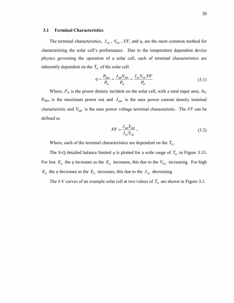
30
3.1 Terminal Characteristics
The terminal characteristics, SCJ , OCV , FF, and η, are the most common method for
characterizing the solar cell’s performance. Due to the temperature dependent device
physics governing the operation of a solar cell, each of terminal characteristics are
inherently dependent on the OT of the solar cell.
Max SC OCMP MP
In In In
P J V FFJ V
P P P (3.1)
Where, Pin is the power density incident on the solar cell, with a total input area, AT,
PMax is the maximum power out and MPJ is the max power current density terminal
characteristic and MPV is the max power voltage terminal characteristic. The FF can be
defined as
MP MP
SC OC
J VFF
J V . (3.2)
Where, each of the terminal characteristics are dependent on the OT .
The S-Q detailed balance limited η is plotted for a wide range of OT in Figure 3.15.
For low GE the η increases as the GE increases, this due to the OCV increasing. For high
GE the η decreases as the GE increases, this due to the SCJ decreasing
The J-V curves of an example solar cell at two values of OT are shown in Figure 3.1.

31
Figure 3.1. Example J-V curves of a solar cell at two values of OT . In most solar cells the
SCJ increases as the temperature increases, while the OCV and FF typically decrease as
the temperature decreases.
In most solar cells, the SCJ goes up as the temperature increases, while the OCV and
FF decrease as the temperature decreases. The SCJ of a solar cell generally increases due
to the temperature dependent bandgap narrowing, which can increase the photon
absorption. The SCJ can also decrease as the temperature increases, when there is
bandgap narrowing in a filter layer or there is an optical element which is impeding the
absorption of additional photons. This will be explained in Section 3.1.4. The
temperature dependent decrease of the OCV and FF are primarily due to the increasing
OJ and the OT . The FF can also be reduced by additional temperature dependent factors
such as the series resistance, shunt resistance and the biasing point loss, see Chapter 5.
The Pin in Equation (3.1) is weakly dependent on the ambient atmospheric
temperature and is not be affected significantly by the OT of the solar cell.
3.1.1 Temperature Dependent Terminal Characteristics
In addition to the standard terminal characteristics discussed in the previous section,
the temperature dependence of the terminal characteristics, or temperature coefficients as
Voltage [a. u.]
Cu
rren
t D
ensi
ty [
a. u
.]

32
they often called, are often measured [96]. Not only can these measurements be used in
conjunction with non-temperature dependent parameters to predict the performance of the
solar cell over a range of OT , they can also be used to further constrain the possible
values for the material parameters and to verify the device physics used in models. These
characteristics can be used when developing analytical models and detailed numerical
models.
There are two types of commonly used temperature coefficients, the absolute
temperature coefficients and the relative temperature coefficients, shown in Table 3.1.
As will be shown in the following subsections the absolute temperature coefficient,
which is the derivative of each terminal characteristic over OT , will not change
significantly over a ranges of OT . Therefore, when the terminal characteristics are plotted
over OT , they appear to change linearly over a ranges of OT .
Table 3.1
Commonly measured terminal characteristics, along with the associated absolute
temperature coefficient and relative temperature coefficients for each terminal
characteristic.
Terminal
characteristic SCJ OCV
FF
Absolute
temperature
coefficient
SCdJ
dT
OCdV
dT
dFF
dT
d
dT
Relative
temperature
coefficient
1 SC
SC
dJ
J dT
1 OC
OC
dV
V dT
1 dFF
FF dT
1 d
dT
Similar to the terminal characteristics, the temperature at which the absolute
temperature coefficients and the relative temperature coefficients were measured must be
specified for these measurements to be useful.
The terminal characteristics and temperature coefficients have been explored by

33
A useful equation was published by Fan [52] and further utilized by many others [57,
97].
The η absolute temperature coefficient is,
OC SC SC OC SC OC
In In In
V FF dJ J FF dV J Vd dFF
dT P dT P dT P dT
. (3.3)
Each parameter in this equation will be examined in the following sections. The
results of this equation for a wide range of OT are shown in Figure 3.17.
The η relative temperature coefficient is,
1 1 1 1SC OC
SC OC
dJ dVd dFF
dT J dT V dT FF dT
(3.4)
This equation shows that the 1 d
dT
is simply the sum of the other relative
temperature coefficients, and therefore each one equally affects the result. This will be
discussed further in Section 3.1.8. A similar equation can be developed if the MPJ
relative temperature coefficient, 1 MP
MP
dJ
J dT, and MPV relative temperature coefficient,
1 MP
MP
dV
V dT, are known.
1 1 1MP MP
MP MP
dJ dVd
dT J dT V dT
(3.5)
3.1.2 Temperature Dependent Terminal J-V Relationship
Each of the common terminal characteristics can be found on the J-V curve of the
solar cell. An example of a J-V curve was shown in Figure 3.1. Figure 3.2 shows the
circuit diagram of an intrinsic solar cell, which has zero SeriesR and infinite ShuntR .

34
Figure 3.2. Circuit diagram of an intrinsic solar cell
The terminal current density, J, of a solar cell can be obtained by using Kirchoff’s
circuit law.
SC RJ J J (3.6)
The recombination current density, RJ , of a single recombination mechanism inside
of a solar cell can be analytically modeled using an intrinsic non-ideal diode equation.
exp 1R
m
O
qVJ
nJ
kT
(3.7)
Where V is the intrinsic terminal voltage, mn is the diode ideality factor, k is
boltzmann constant and OT is the temperature. The OJ is strongly temperature
dependent. The mn can also change over OT , if the dominate recombination mechanism
changes as the OT increases. Section 3.1.4 will discuss the SCJ and Section 3.1.5 will
discuss the OJ . The GE is needed in order to calculate the SCJ and OJ .
3.1.3 Bandgap Energy
The bandgap energy is a material dependent parameter that has been measured for
common semiconductor materials over OT . A variety of fits have been developed to
estimate the bandgap energy of a given material over a wide range of temperatures. The
bandgap energy has been measured to over 500 °C for Si [98, 99], 800 °C for GaAs [100,
101], 900 °C for GaP [100] and 400 °C for SiC [102]. The material specific fit for Si is
J V
JSC JR

35
compared to measurements in Figure 3.3. The fits for additional materials have been
compared to measurements by Passler [103].
Figure 3.3. The material specific temperature dependent
bandgap narrowing fit for Si compared to measurements.
Since the bandgap energy varies significantly over the OT range of interest, it would
be convenient to plot the simulated GE at a single temperature, such as 25 °C. This
would require a single fit that estimates the temperature dependent bandgap narrowing
over the range of simulated bandgaps and OT . A model was previously developed by the
author for use over short OT ranges [104]. This fit is useful for small temperature ranges,
and the OCV estimated using this model was accurate to within 1/2kT from 250 K to 350
K. More about this model can be found in Section B.2.1.
A related model was later developed to estimate the bandgap energy over a similar
range of temperatures [105]. This fit also works well over a smaller range of operating
temperatures. In order for the bandgap energy at each temperature to be adjusted back to
a single temperature, such as 25 °C, a fit is needed that will work over a wider range of
temperatures.

36
The material specific temperature dependent fits for a wide range of semiconductor
materials are shown in Figure 3.4(a) [106]. The temperature dependent bandgap
narrowing relative to 25 °C is shown in Figure 3.4(b). Many of the material specific fits
plotted in the figure have been extrapolated beyond the measured data used to create the
material specific fit.
Figure 3.4. The material specific temperature dependent GE narrowing fits for a wide
range of direct and indirect bandgap semiconductor materials [106]. Many of the
material specific fit plotted in the figure have been extrapolated beyond the measured
data used to create the fit.
For a small range of temperatures near 25 °C, the amount of variation between
materials is small relative to the total bandgap. This coupled with the exponential
bandgap dependence of in made it possible to develop a OJ model over a small range of
temperatures, however, for this work a very wide range of simulated bandgap energies
are needed. The spread of the temperature dependent bandgap narrowing at 800 °C is
larger than the total temperature dependent bandgap narrowing between 25 °C and 800 °C
of many of the materials.
(a) Material specific fits (b) Relative to 25 °C

37
Other methods were used to evaluate the temperature dependent GE narrowing, such
as dividing the temperature GE narrowing by the GE at 25 °C to see if the narrowing
could be normalized. Unfortunately, due to the fact that both narrow and wide bandgap
materials have small and large temperature dependent GE narrowing, each operating
temperature GE can have more than one 25 °C
GE , so the best that a fit can do is offer a
range of possible room temperature GE for each operating temperature GE .
These semiconductor materials represent a wide range of semiconductor types,
which include direct and indirect bandgap materials, single element and compound
semiconductors, a wide variety of lattice spacing and atom sizes, binding energies, as
well as crystal structures. Due to all of these factors, it is not possible to develop a simple
analytical fit that does not incorporate these factors. If a fit was developed, which did
incorporate all of these factors, it could not be used to predict the bandgap narrowing
between measured semiconductors. In addition, such a model would predict more than
one possible bandgap at each bandgap for a single operating temperature; which defeats
the purpose of the model. It was therefore determined that the best way to proceed with
this model is by reporting the result at the operating temperature bandgap and not
adjusting them back to a single temperature.
It is possible to develop a temperature dependent bandgap narrowing fit for a limited
set of semiconductor materials, such as ternary and quaternary compounds made with
GaAs and InP, which will likely have similar narrowing factors. This type of fit could be
used to optimize the bandgap once a material system has been chosen.
A generic fit for all materials could not be found. The examples used in this Chapter
will be examined for three different cases, no temperature dependent GE narrowing,
moderate temperature dependent GE narrowing, Figure 3.5(a), and high temperature
dependent GE narrowing, Figure 3.5(b). The moderate case roughly corresponds to the
average temperature dependent GE narrowing in Figure 3.4(b), and the high case
approximates the CdSe, which was found to have the largest temperature dependent GE
narrowing of the measured materials.

38
Figure 3.5. Generic fit for moderate temperature dependent GE narrowing (a), and high
temperature dependent GE narrowing (b).
3.1.4 Short Circuit Current
The SCJ is a terminal characteristic that may be used to determine how well a solar
cell is converting available photons into current. While it is common that the SCJ of a
solar cell will increase as the temperature increases, this is not always the case. As the
OT of the solar cell increases, there are factors that will cause the SCJ to increase and
there are factors that will cause the SCJ to decrease. Whether the SCJ will increase or
decrease depends on which one is changing faster.
There are many factors that can cause the SCJ to increase as the temperature
increases. One of the many factors that will cause the SCJ to increase is the bandgap
narrowing in the absorbing layers of the solar cell. Since a solar cell can usually absorb
more photons with a narrower bandgap this will cause the SCJ to increase. This increase
will not occur if there is an absorption band between the lower temperature bandgap and
the higher temperature bandgap. Optical elements such as the anti-reflectance coatings
(ARC), as well as other filtering or reflecting optics can reduce the photons available
(a) Moderate narrowing (a) High narrowing

39
below the bandgap at the lower temperature, which will reduce the photons that will be
absorbed by the solar cell, and thereby reduce the rate at which the SCJ will increase.
Another way in which the SCJ of a solar cell can increase as the temperature increases
occurs when the SCJ of one junction is limited by the other junctions in the tandem stack.
If the SCJ of a limiting junction increases, it will increase the SCJ of the other junctions
in the stack. The opposite can also occur when the SCJ of one junction is reduced when
the SCJ of another junction decreases as the temperature increases.
In addition to the factors that will increase the SCJ of a solar cell as the temperature
increases, there are additional internal and external factors that will decrease the SCJ as
the temperature increases. One of the main ways in which this will occur is when the
bandgap of a layer above the absorbing layers of the solar cell also narrows as the
temperature increases. This can occur in many different types of layers, such as the dead
layer at the front of the emitter, a passivation layer, a conducting layer, a window layer,
an ARC layer, another solar cell junction, or another optical component which has
temperature dependent absorption of energies in the solar spectrum. At higher
temperatures the free carrier absorption in these layers may also become important.
Internal factors that can reduce the SCJ as the temperature increases include parameters
such as the diffusion length which can decrease as the temperature increases.
As will be discussed in Section 3.1.3, the temperature dependent GE narrowing is
material dependent. Therefore, the results in this Chapter will be examined for three
different cases, no temperature dependent GE narrowing, moderate temperature
dependent GE narrowing, and high temperature dependent GE narrowing.
While more elaborate methods have been devised to calculate SCJ more accurately
[107]. These methods include incorporating the incomplete absorption and angle
dependencies. The very high temperatures model will assume that all of the photons with
energy larger than the bandgap can be converted into current and that there is no other
factor increasing or decreasing the SCJ as the temperature increases, and each photon can

40
only generate one electron-hole pair. This method is often used to calculate the SCJ . In
addition, many methods are being developed to increase the absorption near and even
below the bandgap, such as multiple-exciton generation, intermediate band cells and
quantum wells [27]. While each of these approaches have limitations, they may
eventually lead to the SCJ values that are equal to or greater than the SCJ value
calculated using this method.
The SCJ is defined as,
0 ( )
/GSCJ q d
hc
. (3.8)
Where, q is the electric charge, is the photon flux density incident on the front
surface of the solar cell, h is Plank’s constant, c is the speed of light, is the photon
wavelength, G is the semiconductor bandgap wavelength, E is the photon energy.
The can be found by using the Plank relation
/hc E (3.9)
Since the results in this work include concentrated cases, the ASTM Standard G173-
03 direct solar spectrum (AM 1.5 (d) will be used [108], Figure 3.6(a). This solar
spectrum is commonly used to evaluate solar cell concentrator systems. The PIn for this
1-Sun spectrum is 90 mW/cm2. The SCJ and PIn will be multiplied by the solar
concentrations, X.
The SCJ and Pin available above a given bandgap are plotted over bandgap in Figure
3.6(b),(d), for the AM 1.5 D standard spectrum. Figure 3.6(c) shows the PIn above the
simulated GE divided by the total PIn. The steps in the plotted lines, Figure
3.6(b),(c),(d), are caused by the absorption gaps in the solar spectrum, Figure 3.6(a).

41
Figure 3.6. Spectral irradiance (a), power available above the simulated GE (b), fraction
of power above the simulated GE (c), and 1-Sun SCJ available above the simulated GE
in the ASTM Standard G173-03 direct spectrum (AM 1.5 D) (d) [108]
A moderate concentration of 500 Suns was chosen for the results in this chapter.
The SCJ available above the simulated GE is shown in Figure 3.7. Because the SCJ is
plotted for the GE at the simulated OT , the plotted SCJ does not change with temperature.
(a) ASTM Standard G173-03 [108]
(b) Power density above the simulated EG
(c) Fraction of power above the simulated EG
(d) The JSC above the simulated EG

42
Figure 3.7. The integrated SCJ available above the simulated GE at 500 Suns.
Due to the irregularities of the solar spectrum shown in Figure 3.6(c), the the SCJ
absolute temperature coefficient, SCdJ
dT, and the SCJ relative temperature coefficient,
1 SC
SC
dJ
J dT, will be found numerically. Figure 3.8 shows the SCdJ
dT and
1 SC
SC
dJ
J dT values
when there is no T dependent GE narrowing (a) & (b), moderate T dependent GE
narrowing (c) & (d) and high T dependent GE narrowing (e) & (f). The T dependent
variation of the SCJ is relatively small compared to the variation caused by the
absorption gaps in the solar spectrum.

43
Figure 3.8. The the SCdJ
dT and
1 SC
SC
dJ
J dT values for cases with no T dependent GE
narrowing (a) & (b), moderate T dependent GE narrowing (c) & (d) and high T
dependent GE narrowing (e) & (f). The T dependent variation of the SCJ is relatively
small compared to the variation caused by the absorption gaps in the solar spectrum.
(b) No T dependent EG narrowing
(a) No T dependent EG narrowing
(c) Moderate T dependent EG narrowing
(d) Moderate T dependent EG narrowing
(e) High T dependent EG narrowing
(f) High T dependent EG narrowing

44
3.1.5 Recombination Current Density
The OJ is one of the primary parameters controlling the FF and OCV of most high
quality solar cells. Approaches have been developed to reduce the OJ of these
recombination mechanisms. The easiest way to reduce the OJ of all of these
recombination mechanisms is to reduce the thickness of the solar cell. The radiative
recombination can be reduced by incorporating light management techniques. The
simplest way to do this is to create a reflective surface on the back surface of the solar
cell. This reflects the radiatively generated photons that could have escaped through the
back surface of the solar cell. The radiative recombination can be reduced by more than
a factor of 10 using light trapping and photon recycling [109, 110]. The upper limit on
reducing the radiative recombination is the Shockley-Queisser detailed-balance limit. A
number of methods have been developed to calculate the Shockley-Queisser detailed-
balance limit. Levy developed a method for calculating the detailed-balance saturation
current using Riemann zeta functions [86]. An simple to use analytical expression was
developed by Gray [87].
3 2
/
3 2
22 2GE kT G G
O
kT E EJ q e
h c kT kT
(3.10)
This expression has a high degree of accuracy for solar cell devices with GE above
>3kT, which is ~77 meV at 25 °C and ~277 meV at 800 °C. The highest order polynomial
term will dominate the other two at higher GE values. The results of this equation
plotted over a range of GE from 0.5 eV to 3 eV and OT from 25 °C to 800 °C are shown
in Figure 3.9. The OJ increases exponentially as the OT increases, it also increases
roughly OT to the 3/2 power.

45
Figure 3.9. The OJ at the simulated GE for 500 Suns. The OJ increases as the OT
increases and the OJ increases exponentially as the GE decreases.
Due to the multiple temperature dependencies in Equation (3.10), it is difficult to
identify the dominate components of the OJ absolute temperature coefficient,
2
/2
2
2
2
/3
2 2
/3
2 3
2
3 2 2
12 2
2 2 22
G
G
G
E kTO G G
E kTG G G G
E k GT G G G G
d
kT dT
E dE E dE E
k T dT k T kT dT
dJ E EH T e
dT kT kT
E E E EHT e
kT kT kT
Hk
eT
T
,
(3.11)
where, H contains the constant parameters in Equation (3.10).
Dividing Equation (3.11) by Equation (3.10) to find the relative temperature
coefficient, 1 O
O
dJ
J dT, simplifies the first two terms in Equation (3.11). However, the 3
rd
term is more complicated. This makes it difficult to interpret the temperature
dependencies of this equation.
2 2
2
2 2 2 3 21 3
2 2
1
2 2
2 2
O G
G G G
G
O G G
G GE dE E dE E
kdJ E T dT k TE kT dT kTd
kJ dT T T dT kT E E
kT kT
(3.12)
(d) JSC above the

46
Understanding the temperature dependencies of Equations (3.11) and (3.12) will
require the GdE
dT and
1 G
G
dE
E dT to be found in Section 3.1.3, for moderate temperature
dependent GE narrowing and high temperature dependent GE narrowing. For
semiconductor materials with little or no temperature dependent GE narrowing.
Equation (3.11) simplifies to
2 2
/3
22
232GE kTO G G G G GE
T
dJ E E E EHT e
dT T kkT kT kT k TT
,
(3.13)
and Equation (3.12) simplifies to
2
2 2
2
1 3
2 2
G
O G
O G G
GE
T kTdJ E
J dT T kT E
E
kT
E
kT kT
.
(3.14)
Figure 3.10 shows the OdJ
dT and
1 O
O
dJ
J dTwhen there is no temperature dependent GE
narrowing (a) & (b), moderate temperature dependent GE narrowing (c) & (d) and high
temperature dependent GE narrowing (e) & (f). The OdJ
dT increases and the
1 O
O
dJ
J dT
decreases quickly as the GE decreases and the OT increases.

47
Figure 3.10. The OdJ
dT and
1 O
O
dJ
J dTvalues for cases with no T dependent GE narrowing
(a) & (b), moderate T dependent GE narrowing (c) & (d) and high T dependent GE
narrowing (e) & (f). The OdJ
dT increases and
1 O
O
dJ
J dT decreases quickly as the GE
decreases and the OT increases.
(b) No T dependent EG narrowing
(a) No T dependent EG narrowing
(c) Moderate T dependent EG narrowing
(d) Moderate T dependent EG narrowing
(e) High T dependent EG narrowing (f) High T dependent EG narrowing

48
Simpler equations for OdJ
dT and
1 O
O
dJ
J dTcan be found by further simplifying
Equation (3.10). This simplification is helpful to get a sense of the overall temperature
dependencies of the OJ .
2
/3 GE kT GO
EJ HT e
kT
(3.15)
This expression is 10% lower than Equation (3.10) above 20kT, which is ~0.5 eV at
25 °C and ~1.8 eV at 800 °C.
The OdJ
dT of Equation (3.15) is then,
2/
2 2
2 11GE kTO G G G
G
G
dJ E dE dEHTe E
dT k T E dT dTk Tk
,
(3.16)
and the 1 O
O
dJ
J dT is then,
2
21 11O G G G
O G
dJ E dE dE
J dT T Ek TkdT dT
. (3.17)
For semiconductor materials with little or no temperature dependent GE narrowing
Equation (3.16) simplifies to
/
2 2
2 1GE kTO GG
dJ EHTe E
dT k T k
,
(3.18)
and Equation (3.17) simplifies to
2
11O G
O
dJ E
J dT T k
. (3.19)
The 1 O
O
dJ
J dT is therefore approximately equal to
2
GE
T k, since the
2
GE
T k term will be
larger than the unity term in this equation, for all of the GE values where Equation (3.15)
is a good approximation of OJ , see Figure 3.10(b). The GE decreases slowly as the OT
increases and the OT increases to the 2 power as the OT increases. The same

49
simplification can also be applied to Equation (3.18) to examine the temperature
dependent of the OdJ
dT, see Figure 3.10(a).
3.1.6 Open Circuit Voltage
This chapter focuses on finding the terminal characteristics and terminal coefficients
of the S-Q detailed balance limit, which has only one recombination mechanism,
Equation (3.10). Methods for calculating the OCV with more than one recombination
mechanism will be discussed in section 4.1.1. The OCV for a single dominate
recombination mechanism can be found by solving for V in the intrinsic non-ideal diode
equation, Equation (3.6), when J is zero.
ln 1SCOC
O
JnkTV
q J
(3.20)
In this equation the OJ reduces the OCV faster than the OT term or SCJ can increase
it. This causes the OCV to decrease for a given GE as the OT increases. Due to the
exponentially increase of OJ as the GE decreases, the OCV decreases nearly linearly as
the GE decreases.

50
Figure 3.11. The OCV at the simulated GE for 500 Suns. As the OT increases the OCV
decreases for a given GE at OT , this is caused by OJ . The OCV increase nearly linearly
as the GE increases.
The OCV absolute temperature coefficient, OCdV
dT, can be found from Equation
(3.20).
1ln lnSOC C SC O
SC O O
SC O O SC O
dJ J dJJ J J T
J J dT
dV n
J J J d
k nkT
T q Td q
(3.21)
Since the OCdV
dT is negative in all three T dependent GE narrowing cases, Figure
3.12(a),(c),(e), the second term which is negative must be significantly larger than the
first term. It is unlikely that the first term will be negative, due to the fact that the SCdJ
dT
is usually positive, Figure 3.8.
The OCV relative temperature coefficient is,
1 1
ln ln
SC SC O
O
SC O SC O O
OC
OC
dJ J dJ
dT J dT
J J J J J
dV
V dT T
.
(3.22)
(f) High T dependent

51
Figure 3.12(b),(d),(f) shows that the 1 OC
OC
dV
V dT is negative in all three cases, which
means that the SC O
O
J dJ
J dT term must be larger than the SCJ
dT term. The denominator of the
second term is expected to always be positive, since the natural log of SCJ + OJ will be
larger than the natural log of OJ .

52
Figure 3.12. The OCdV
dT and
1 OC
OC
dV
V dT values for cases with no T dependent GE
narrowing (a) & (b), moderate T dependent GE narrowing (c) & (d) and high T
dependent GE narrowing (e) & (f). The OCdV
dT becomes more negative as the GE
increases and as the OT increases. As OT dependent GE narrowing increases, the dFF
dT
(b) No T dependent EG narrowing (a) No T dependent EG narrowing
(c) Moderate T dependent EG narrowing
(d) Moderate T dependent EG narrowing
(e) High T dependent EG narrowing (f) High T dependent EG narrowing

53
becomes less sensitive to the OT . The 1 dFF
FF dT becomes more negative as the GE
decreases, as the OT increases and as the GE narrowing increases.

54
The OCdV
dT, Equation (3.21), can be simplified by assuming that the SCJ is
significantly larger than OJ . This is true for
GE values above 0.5 eV at 200 °C and GE
values above 1.5 eV at 800 °C, Figure 3.9.
n ln11
l SC OSC
CO
S O
O
C
dJ dJJ T J T
J d
dV nk nk
T J dTdT q q
(3.23)
And the simplified 1 OC
OC
dV
V dT is,
1
l
1
n ln
1 1
SC O
SCC O
OO S
O
C C
dJ dJ
J dT J dT
J
dV
V dT JT
.
(3.24)
3.1.7 Fill Factor
The FF, defined in Equation (3.2), is an important catch all terminal characteristic
that is affected by device parameters such as n, SeriesR and ShuntR .
The MPJ and MPV of the intrinsic single diode case can be found by using Equation
(3.6) and Equation (3.7).
exp 1MP
MP SC O
qVJ J J
nkT
(3.25)
An analytically intrinsic FF is solution as well as other analytical solutions were
developed by Green [111].
ln 0.72
1
OC OC
OC
qV qV
nkT nkTFF
qV
nkT
(3.26)
Analytical and numerical methods for calculating the FF for various combinations of
resistances, multiple diodes in parallel and number of solar cell junctions in series is
discussed in Appendix C. The S-Q detailed balance limit FF is shown in Figure 3.13.
The denominator in Equation (3.26) will always be positive, because the OCV is always

55
positive, Figure 3.11. Since the FF is always positive the first term is always larger than
the second term.
Figure 3.13. The FF at the simulated GE for 500 Suns. As the OT increases the FF
decreases for a given GE at OT , this is caused by OJ .
The FF absolute temperature coefficient, using Equation (3.2) is,
2 2
SC OCMP MP MP MP MP MP MP MP
SC OC SC OC SC OC SC OC
dJ dVJ dV V dJ J V J VdFF
dT J V dT J V dT J V dT J V dT (3.27)
Solving this equation requires the values MPJ , MPV , MPdJ
dT and MPdV
dT. All three
cases of GE narrowing in Figure 3.14 show that this equation is negative. As expected
the value of dFF
dT becomes more negative as the GE decreases. It also becomes more
negative as the OT increases and the GE narrowing increases.
The FF absolute temperature coefficient, using the analytical equation is,
(f) High T dependent

56
2
2
2 0.72
11
OC OC
OC OC
OC OCOC
OCOC
dV qVq
dV qVqnkT dT nkTqV dVq qV nkT dT nkTnkT nkT dTdFF nkT
qVqVdT
nkTn
F
kT
F
(3.28)
The FF relative temperature coefficient, using Equation (3.2) is,
1 1 1 1 1SC OCMP MP
MP MP SC OC
dJ dVdV dJdFF
FF dT V dT J dT J dT V dT (3.29)
Just like dFF
dT the
1 dFF
FF dT is negative in all three cases in Figure 3.14. In Equation
(3.29) the first and the third terms are negative while the second and the fourth terms are
positive.
The FF relative temperature coefficient, using analytical equation is,
2 20.3
1
1 0.7 ln 0.72
OC OC OC OC OC
OC OC OC OC
qV dV qV qV dVq q
nkT nkT dT nkT nkT nkT dTdFF
qVFF dT qV qV qV
nkT nkT nkT nkT
,
(3.30)
The denominator of both terms will always be positive, the first term is obvious and
the second term won’t become negative, because the numerator of Equation (3.26) cannot
be negative.
The result if the FF term is not substituted.
20.7 0.3
1
0.7 1
OC OC OC OC
OC OC
qV dV qV qVqFF FF
nkT nkT dT nkT nkTdFF
qV qVFF dTFF
nkT nkT
(3.31)

57
Figure 3.14. The dFF
dT and the
1 dFF
FF dT values for cases with no T dependent GE
narrowing (a) & (b), moderate T dependent GE narrowing (c) & (d) and high T
dependent GE narrowing (e) & (f). Similar to the OCV temperature coefficients, Figure
3.12, the dFF
dT and the
1 dFF
FF dT both becomes more negative as the GE decreases, as
the OT increases and as the GE narrowing increases.
(a) No T dependent EG narrowing
(a) No T dependent EG narrowing
(c) Moderate T dependent EG narrowing (d) Moderate T dependent EG narrowing
(d) High T dependent EG narrowing (e) High T dependent EG narrowing

58
3.1.8 Conversion Efficiency
The most important terminal characteristic is the PMax, which is often measured
relative to the PIn, to give the η, Equation (3.1). The temperature dependencies of SCJ ,
OCV , and FF all affect the η. In most cases as the OT increases the η decreases, however
this is not always the case. For lower values of GE , the η increases as the
GE increases,
this is caused by the increase in the OCV , Figure 3.15. For higher values of GE , the η
decreases as the GE increases, this is caused by the decrease in the SCJ . This balance
between the SCJ and the OCV , causes the GE of the optimal peak η to increase as the OT
increases. In addition the 25 °C GE will be at a higher GE , due to the T dependent GE
narrowing.
Each η curve in Figure 3.15 has an optimal peak as well as multiple local maxima.
The optimal peak η over OT is shown in Figure 3.16. The multiple peaks are caused by
the absorption gap in the solar spectrum, which are shown in Figure 3.6(a). Because the
η decrease more quickly for lower GE devices, these peaks will lead to steps in the
simulated GE over OT of the optimal peak η. The effect of these steps will be explored
in Section 4.3.3.
The η plot also shows that solar cells which approach the S-Q detailed balance limit
could have high η at high OT . These results show that it is possible to reach 29 % at
400 °C and 20 % at 800 °C. At high OT , real devices will likely be limited by other
factors before reaching these high η values.

59
Figure 3.15. The η at the simulated GE for 500 Suns. As the OT increases the η
decreases for a given GE at OT . In most values of GE as the OT increases the η
decreases. For lower values of GE , the η increases as the GE increases, this is caused by
the increase in the OCV . For higher values of GE , the η decreases as the GE increases,
this is caused by the decrease in the SCJ .
Figure 3.16. The optimal peak η over OT for a concentration of 500 Suns. As the OT
increases the η decreases.
(f) High T dependent
(f) High T dependent

60
The d
dT
, as defined in Equation (3.3), and
1 d
dT
, as defined in Equation (3.4), are
typically negative for most GE values, Figure 3.17. However, for high GE values it is
possible that the temperature dependence of the SCJ will cause the d
dT
and
1 d
dT
to be
positive. This can be seen by comparing the relative temperature coefficient terms in
Equation (3.4). At high GE values both 1 OC
OC
dV
V dT and
1 dFF
FF dT become small, while at
the same time the 1 SC
SC
dJ
J dT is becoming larger, leading to a positive
1 d
dT
.
In S-Q detailed balance limited solar cells this occurs above 2 eV in solar cells with
moderate T dependent GE narrowing and above 1.75 eV in solar cells with high T
dependent GE narrowing.

61
Figure 3.17. The d
dT
and
1 d
dT
values for cases with no T dependent GE narrowing (a)
& (b), moderate T dependent GE narrowing (c) & (d) and high T dependent GE
(b) No T dependent EG narrowing
(a) No T dependent EG narrowing
(c) Moderate T dependent EG narrowing
(d) Moderate T dependent EG
narrowing
(e) High T dependent EG narrowing (f) High T dependent EG narrowing

62
narrowing (e) & (f). The 1 d
dT
is the sum of the
1 SC
SC
dJ
J dT,
1 OC
OC
dV
V dT and
1 dFF
FF dT,
this causes the S-Q detailed balance limited d
dT
and
1 d
dT
to be positive above 2 eV in
solar cells with moderate T dependent GE narrowing and above 1.75 eV in solar cells
with high T dependent GE narrowing.

63
The S-Q detailed balance limit over simulated GE and OT has been evaluated in
Section 3.1. These results are particularly useful in understanding how the terminal
characteristics and temperature coefficients vary over GE and OT . The peak η for a given
OT was also determined. In addition, these results provide insight into what level of
performance is available for solar cells that approach this limit. The next section will
look at the S-Q detailed balance limited terminal characteristics using measured T
dependent GE narrowing of real semiconductor materials.
3.2 Real Semiconductor Materials
It is important to know how solar cells will perform at high OT , when planning,
designing and optimizing solar cell systems that operate at high OT . While the
temperature dependence of the terminal characteristics are nearly linear near room
temperature, care must be taken when extending these results to higher OT , where the
performance is no longer linear. This section will explore how the physical material
property, T dependent GE narrowing, of real materials will affect the η over a wide range
of OT . These results are particularly useful in understanding how the T dependent GE
narrowing will affect the semiconductor material chosen and the optimization of the high
temperature systems.
3.2.1 Extrapolating the Temperature Coefficients
The T dependence of the terminal characteristics are often thought to vary linearly
over OT . While this is true of solar cells over a narrow range of OT , it frequently does
not hold over a wide range of OT . For solar cells operating near the S-Q detailed balance
limit, this is due primarily to the T dependent GE narrowing. Therefore, generally solar
cells with larger T dependent GE narrowing will deviate more quickly away from the
linear trend, than solar cells with smaller narrowing.

64
There are four cases in which the η of real materials deviate from the linear trend,
Figure 3.19 and Figure 3.19. The black lines are the S-Q detailed balance limit η for each
material, using the published T dependent GE narrowing for each of the materials. The
red line is the linear extrapolated η at 25 °C. The dips in the black line are caused by the
absorption gaps in the solar spectrum.
Figure 3.18. The black lines are the S-Q detailed balance limit η for each material, using
the T dependent GE narrowing for each of the materials. The red lines are the linear
extrapolated η at 25 °C. The dips in the black line are caused by the absorption gaps in
the solar spectrum. For wide GE materials such as GaN (a), the S-Q detailed balance
limit η can increase faster than the linear extrapolated η at 25 °C as the OT increases. For
some moderate EG materials such as ZnTe (b), the η can increase as the OT increases at
lower temperatures, due to the T dependence of the SCJ and then decrease as the OT
increases at higher temperatures, due to the T dependence of the OCV . The lower EG
materials, SiC, GaAs, Si and Ge are plotted in Figure 3.19
(a) GaN (b) ZnTe

65
Figure 3.19. The black lines are the S-Q detailed balance limit η for each material, using
the T dependent GE narrowing for each of the materials. The red lines are the linear
extrapolated η at 25 °C. The dips in the black line are caused by the absorption gaps in
the solar spectrum. For the moderate GE material SiC (a), the η simulated using the S-Q
detailed balance limit and the linear extrapolated η at 25 °C are almost exactly the same.
For GaAs (b), the S-Q detailed balance limit η decreases faster than the linear
extrapolated η at 25 °C as the OT increases. As was the case with SiC (a), the Si (c) η
simulated using the S-Q detailed balance limit and the linear extrapolated η at 25 °C are
almost exactly the same. For low GE materials such as Ge (d), the S-Q detailed balance
limit η decreases slower than the linear extrapolated η at 25 °C as the OT increases. The
Higher GE materials, GaN and ZnTe are plotted in Figure 3.19
For each of the materials plotted in Figure 3.19 and Figure 3.19, the η simulated
using the S-Q detailed balance limit and the η linear extrapolated from 25 °C are nearly
(a) SiC (b) GaAs
(c) Si (d) Ge

66
identical from 0 °C to 100 °C. Above this temperature the linear extrapolated η of many
of the materials begans to deviate from the η simulated using the S-Q detailed balance
limit and the T dependent GE narrowing for each material. The materials can be
seperated into 4 different cases.
The first case occurs in wide GE materials such as GaN, Figure 3.18(a). Here the η
increase faster than the T dependent η linearly extrapolated from 25 °C, which agrees
with the results in Figure 3.17 for semiconductors with moderate and high T dependent
GE narrowing. This is due to the 1 SC
SC
dJ
J dT term, Figure 3.8(d) and (e), being larger than
the 1 OC
OC
dV
V dT and
1 dFF
FF dT terms, Figure 3.12 and Figure 3.14.
In the second case, the η of moderate GE materials, such as ZnTe (b), will first
increase and then decrease as the OT increases. The η begins to decrease when the
1 OC
OC
dV
V dT and
1 dFF
FF dT terms become larger than the
1 SC
SC
dJ
J dT term.
For both SiC Figure 3.19(a) and Si (c) the η simulated using the S-Q detailed balance
limit and the linear extrapolated η at 25 °C are almost exactly the same over the simulated
OT range. This may be primarily due to the smaller η over OT bumps in both of these
material, which are caused by the 1 SC
SC
dJ
J dT.
The third case occurs in materials such as, GaAs Figure 3.19(b). In these materials
the η decreases more quickly than the linear fit. The 1 SC
SC
dJ
J dT which is improving the
1 d
dT
at lower OT , is causing the linear extrapolated η at 25 °C to predict η values that
are higher than the η simulated using the S-Q detailed balance limit at higher OT .
In the forth case, which occurs in narrow GE materials such as Ge (d), the S-Q η
decreases more slowly than the linear fit. The 1 SC
SC
dJ
J dT is improving the
1 d
dT
at

67
higher OT , which is causing the linear extrapolated η at 25 °C to predict η that are lower
than the the η simulated using the S-Q detailed balance limit at these higher OT .
Figure 3.19 and Figure 3.19 showed that the linearly extrapolated η at 25 °C was
very accurate for most semiconductor materials with OT up to 100 °C. It was also shown
that the linearly extrapolated η, was not as accurate for OT above 100 °C.
3.2.2 Finding the Optimal Material
Even when modeling the relatively simple S-Q detailed balance limit, finding the
optimal material is complicated by the T dependent GE narrowing and the absorption
gaps in the solar spectrum. In addition, while the T dependent GE narrowing causes the
GE of real semiconductor materials to decrease as the OT increases, the GE of the
optimal peak found in Section 3.1.8, Figure 3.15, increases as the OT increases.
Therefore, without developing a material in which the GE widened as the OT increased,
no material will be at the optimal peak η over a broad OT range. This will be discussed
more in Section 3.2.3. There are a number of ways around this problem.
One way of mitigating this problem would be to switch the solar cell at the focal
point of the concentrator system. In such a system, a lower GE solar cell would be
placed at the focal point of the concentrator when the system is operating at a lower OT .
As the OT increases one or more additional solar cells with wider GE , that are closer to
the optimal peak η, would be places at the focal point of the concentrator. This would
allow the system to operate closer to the optimal peak η over a wider OT range. Because,
this is expected to significantly increase the cost of the system, it is improbable that this
would be a viable solution.
Another way of mitigating this problem would be to identify a solar cell with a GE
that allowed it to performed best over the desired OT range. Figure 3.20(a) compares the
S-Q detailed balance limited η of five wide GE materials with optimal peak η (Figure

68
3.16). The η of these wide GE materials are nearly flat, because the T dependent increase
of the SCJ is compensating for the decrease of the OCV and FF. None of these materials
reach the peak η line below 800 °C.
Figure 3.20. The η calculated using the T dependent GE narrowing of real materials,
compared to the optimal peak η calculated in Section 3.1.8. The high GE material (a)
does not reach the optimal peak η, while the moderate GE materials will reach the
optimal peak η.
Figure 3.20(b) examines the η of the five moderate GE materials. Each of these
materials approaches the optimal peak η line at different OT points. The materials with
wider GE , such as CdSe, materials do so at higher OT and the materials with narrower
GE materials such as Si, are at lower OT . CdSe, CdTe, GaAs and InP are all relatively
close to the optimal peak η line from 400 °C to 800 °C. Above 400 °C CdSe is nearly
constant while the other materials continue to increase. If the solar cell was needed to
operate at 425 °C, CdSe would give the highest η. However, it would not perform as well
if the system operated between 300 °C and 450 °C. It is therefore important to consider
the full range of OT where the solar cells will be operating.
(a) Wide EG materials (b) Moderate EG materials

69
Due to the steps in the optimal peak GE , which will be explained in Section 4.3.3,
some of the materials do not reach the optimal peak η. There is a wide range of OT , from
150 °C to 300 °C, over which these materials are more than 0.8 absolute % points below
the optimal peak η, Figure 3.21. There are also points at 180 °C and 270 °C that are more
than 1 absolute % point below the optimal peak η. This is primarily due to the steps in
the optimal peak GE , as well as the dearth of elemental and binary compound
semiconductor materials with GE between InP and Si. Using ternary compound
semiconductors such as GaInAs or quaternary compound semiconductors such as
GaInAsP can fill this void.
Figure 3.21. The absolute % difference between the η calculated using the T dependent
GE narrowing of real materials and the optimal peak η calculated in Section 3.1.8. Due
to the steps in the GE at the optimal peak η, not all of the materials reach the optimal
peak η.
The η of real materials cannot go above the optimal peak η, unless the absorption of
the solar cell and the electrical GE are decoupled. A number of research groups are
designing solar cell to absorb photons below electrical GE using with quantum wells and
quantum dots. It may be possible to find a material or a device design where this is
possible [27].

70
3.2.3 Improving the Temperature Coefficients
The η of solar cells over OT and the reliability have a profound effect on the
economics and the LCOE of solar cells. If two solar cells have the same η at one OT , the
one with a better d
dT
will produce more electrical energy at a higher OT . In addition,
areas with higher solar irradiance have the potential to produce more electrical energy.
However, these locations are often hotter, than areas with lower soalr irradiance. It is
possible that the d
dT
of a solar cells could remove the benefit of the higher solar
irradiance, if the higher OT in this location causes the solar cell to operate at a lower η
and generate less electrical energy. Therefore any changes that can be made to the solar
cell that will improve the d
dT
, while at the same time improving or not significantly
reducing the η, will be beneficial.
There are only two parameters that can be modified in a S-Q detailed balance limited
model. One of those is the device thickness, which will affect the absorption and the
emission of the devices. This model does not include this parameter. The other
parameter that can be changed is the GE . There are two ways in which the GE can be
changed. This includes picking the GE at some point such as 25 °C, the other is the T
dependent GE narrowing of the material. While the T dependent GE narrowing is a
physical parameter of the semiconductor material, it might be possible to vary it by
changing other material parameters.
The GE is affected by a number of other material parameters, such as the OT , electric
field strength, strain, pressure and carrier densities. If desirable, it may be possible to
adjust the rate at which the GE varies by adjusting one of these other parameters, such as
exerting pressure on the solar cell [112] or by straining the junction layers, as the OT
increases. In this section, two cases are compared to evaluate if controlling the GE could
be beneficial. In the first case the cell is unmodified, the T dependent GE narrowing

71
reduces the GE . In the second case the GE is held constant over OT . This could be
achieved by varying another parameter over OT , in such a way that it compensates for the
T dependent GE narrowing, such as exerting pressure on the solar cell [112] or by
straining the junction layers.
Figure 3.22 shows how (a) GaN, (b) GaAs, (c) Si and (d) Ge will perform in these
two cases. Holding the GE constant of wide GE material will eliminate the T dependent
SCJ improvement, which will significantly reduce the overall performance as the OT
increases. Holding the GE of GaAs constant reduces the η from 25 °C to 300 °C, has no
affect from 300 °C to 600 °C and then improves the performance above 600 °C. Holding
the GE of Si constant will improve the η one full absolute % above 200 °C. Holding the
GE of Ge constant will significantly improve the η as the OT increases.

72
Figure 3.22. Compares the case with GE narrowing and the case where the GE is held
constant over OT , for (a) GaN, (b) GaAs, (c) Si and (d) Ge. For wide GE materials such
as GaN, holding the GE constant will decreae the performance over OT . For moderate
GE materials, such as GaAs and Si there may be a small improvement or a small loss.
For narrow GE materials, such as Ge, holding the GE constant increases the performance
over OT .
The results presented above compare the cases where the GE narrows as the OT
increases and where the GE is stays constant over OT . The GE at the optimal peak η
increases as the OT increases, therefore in some cases it may be beneficial to design a
(a) GaN
(c) Si
(b) GaAs
(d) Ge

73
solar cell where the GE becomes wider as the OT increases, allowing the solar cell to
operate closer to the optimal peak η over a wider range of OT .
3.2.4 3-D effects
The S-Q detailed balance limit and other diode models, such as the recombination
limited model in Chapter 4, model the solar cell in 1-D. This is possible since the
semiconductor junction is uniform in 2-D in most solar cells. Therefore, a 1-D model can
be used successfully to represent the device physics. These models are particularly useful
in the initial design and planning stages, when it is common to evaluate a large number of
possible solar cell designs. However, these models cannot accurately account for the 3-D
effects occurring in the solar cell.
Two types of 3-D structures commonly used are grid and busbar electrodes. These
3-D structures affect the terminal characteristics and T dependencies of the solar cell,
which will be explored further in Chapter 5. In an effort to boost the η, more elaborate 3-
D designs have been developed for solar cells. These include line and point contacts,
which will also affect the terminal characteristics and the T dependent performance.
The SCJ can be reduced by un-illuminated regions of the solar cell, which act as a
sink for current. Some of the current generated in the illuminated regions will flow
laterally through the solar cell and recombine in the un-illuminated regions.
The OCV can be reduced by circulating currents, which are also caused by current
flowing from the illuminated regions to the un-illuminated regions of the solar cell [113].
This can cause the OCV to be reduced below the value predicted by the 1-D model.
Another important 3-D effect is the joule and bias-point resistive losses, which is
also caused by lateral currents flowing through the LCL. This current causes a voltage
drop which leads to parts of the solar cells being biased away from the ideal PMax.
Each of the terminal characteristics and T dependencies of the solar cell are affected
by the 3-D structures used on solar cells. It is therefore not possible to completely model
the terminal characteristics and T dependencies using a 1-D model.

74
3.3 Summary and Conclusions
Through extensive research efforts, the η of each type of solar cell has improved over
time [13, 47]. This has been achieved by improving the material quality and device
designs. As the η of solar cells improve, they come closer to the S-Q detailed balance
limit. This chapter has identified the terminal characteristics and the T dependent
coefficients that could be achieved by solar cells that approach this limit, over a broad
range of OT and GE . These calculations are particularly helpful in identifying the
potential of solar cells that approach this limit. In addition, this chapter has also shown
that T dependent GE narrowing does not affect all solar cells in the same manner, which
is particularly important when trying to optimize a solar cell operating at high
temperature.
Solar cells that operate at high T would be useful in a wide range of applications,
from high concentration photovoltaic systems, to hybrid thermal photovoltaic systems, to
near sun photovoltaic space probes, to space concentrator photovoltaic systems. This
chapter showed that the T dependent GE narrowing improves the potential η of wide GE
material. While at the same time, it has little effect on moderate GE materials and it will
reduce the η of narrow GE materials. As expected the simulations show that as the OT
goes up the η decreases and the optimal GE at the optimal peak η increases.
In addition, it was found that the optimal GE is strongly affected by the absorption
gap in the terrestrial solar spectrum. This causes steps in the optimal GE over
temperature. It was also shown that there is range of bandgaps near the optimal GE with
η relatively close to the optimal peak η. It was also shown that the temperature
dependence of the optimal GE and the GE of real semiconductor materials have the
opposite slope. However, due to the flat portions of the optimal GE steps, it might be
possible to find a material with an GE , which is close to the optimal GE over a wider
range of OT .

75
After the regions with the peak η and optimal GE have been identified, the material
parameters of real materials can be used to identify candidate materials that are closest to
the optimal peak over the temperature range of interest. The candidate materials can be
further verified using additional detailed numerical models and 3-D models to more
accurately determine the potential of the individual material and develop optimal device
designs. Solar cell fabricators can then use these designs to develop and characterize the
actual solar cells. The measurement data can then be used to improve the models and
identify ways to improve the performance of the solar cells.
Based on these simulations it appears that the η of an appropriately designed solar
cell operating above 300 °C could be quite high. These solar cells could be very useful in
high T applications. The next Chapter will explorer the other bulk recombination
mechanisms which are limiting the η.
3.3.1 Future Work
The calculations in this chapter assume that 100% of the photons above the
simulated GE are absorbed and converted to current. This is useful for determining the
upper limit of the SCJ , for devices that do not absorb photons below the bandgap energy.
This model could be further improved by including realistic partial absorption for direct
and indirect bandgap materials [114]. Doing this could change the optimal peak bandgap
by a few tens of millivolts. It would also allow the thickness of the solar cell to be
studied. Thinning the solar cell will reduce the photogenerated current, and it will also
reduce the volume over which recombination can occur. The optimal thickness could be
found, by varying the thickness at each temperature.
The optical absorption coefficient, , of semiconductors are strongly influenced
by the operating temperature. This has been measured for the direct bandgap material
GaAs over a wide range of photon energies [101] and near the band edge [115].
Therefore it will likely be necessary to include the temperature dependent optical
bandgap narrowing in the absorption model, when optimizing the device thickness. In
addition to being temperature dependent, the optical of semiconductor materials is

76
also doping dependent. However, this dependence is not the same for all materials or
dopants. For p-type GaAs the measured changes very little as the doping
concentration increases from 2x10¹⁷
[cm-3
] to 1.2x10¹⁸
[cm-3
], and for n-type GaAs the
measured varies from that of a direct bandgap material, to an that is more
similar to an indirect bandgap material [116].

77
4. RECOMBINATION LIMITED VERY HIGH
TEMPERATURE TERMINAL CHARACTERISTICS
While the η of solar cells have improved over time, thus moving closer to the S-Q
detailed balance limit discussed in Chapter 3, they are still primarily limited by other
recombination mechanisms. Developing a model that includes these additional loss
mechanisms and can be used over the same very wide range of OT , GE and X would be
particularly useful to program managers and system designers. The model developed in
this chapter can estimate the η that could potentially be achieved based on the measured
bulk recombination parameters of existing materials. This would allow them to
determine if it is technically feasible to reach a certain design goal. The simulated η in
this chapter will be closer to the measured high efficiency world record solar cells than
the S-Q detailed balance limit η simulated in Chapter 3.
This chapter has been divided into four parts. The first part (Section 4.1) will
examine the analytical model used to simulate multiple recombination mechanisms and
the theoretical temperature dependencies of solar cells over OT and GE . The second part
(Section 4.2) will present the semi-empirical material parameter fits needed to simulated
the η over OT and GE . The third part (Section 4.3) will discuss the results of the
analytical simulations. The last part (Section 4.4) will explore additional affects, such as
the 3-D resistivity, that is not incorporated into this model.
4.1 Terminal Characteristics
Similar to Chapter 3, in this chapter an analytical model will be used to simulate the
possible solar cell performance over a very wide range of OT and simulated GE . This
analytical model can incorporate all three of the common bulk recombination

78
mechanisms in solar cells; radiative recombination, Shockley-Hall-Reed (SHR)
recombination, and Auger recombination. Each of these recombination mechanisms can
limit the performance of a solar cell under different conditions. Solar cells with low
material quality are limited by SHR. Direct bandgap materials are often limited by
radiative recombination. And solar cells with high OCV are often limited by Auger
recombination. Methods are being used and investigated to reduce each of these
recombination mechanisms. The first to be reduced is the SHR recombination.
Through extensive research, growth methods have been developed for many
semiconductor materials, such as Si and GaAs, to significantly reduce the SHR
recombination. This has led the SHR recombination to be a small part of the total
recombination in some devices. Because the SHR recombination has continued to
decrease over time, in the results presented in this chapter, it will be assumed negligible.
The radiative recombination and Auger recombination used in this model are based on
semi-empirical fits to the measured values for these material parameters.
4.1.1 Multiple Diode Equation
There are many types of recombination mechanisms inside of solar cells. Some of
these recombination mechanisms such as interface and surface recombination can be
significant in some types of solar cell, and be insignificant in other types of solar cells.
The interface recombination has been reduced to insignificant levels in some solar cells,
through careful growth techniques, which reduce the number of defects present in the
interface. The surface recombination can be reduced through the use of passivation
layers or by adding a heterojunction layer, such as the amorphous Si layer in HIT solar
cells or the GaInP layers in GaAs solar cells.
Three types of recombination are common in most types of solar cells, radiative
recombination, ,RJ , SHR recombination,
,R SHRJ , and Auger recombination, ,R AugerJ .
The extrinsic terminal characteristics of this model, with series resistance, SeriesR , and
shunt resistance, ShuntR , is defined as (Figure 4.1)

79
, , ,SC R R SHR R ASerie
uger
S
s
hunt
V JRJ J J J J
R
. (4.1)
Figure 4.1. Multiple diode circuit diagram, with radiative recombination, ,RJ , SHR
recombination, ,R SHRJ , and Auger recombination,
,R AugerJ , as well as series resistance,
SeriesR , and shunt resistance, ShuntR .
The sum of the recombination currents is
,
, ,
exp 1SeriesR O m
m SHR Auger m
V JRJ J
n kT
. (4.2)
In most cases, when more than one type of recombination is simulated, the MPJ , MPV
and FF cannot be solved analytical. Many researchers have used Newton’s method to
solve for these parameters. A computationally quicker and simpler bisection approach
was developed by Gray to solve for the FF in cases with one or more series connected
junctions each with a single diode, as well as SeriesR , is described in Section C.2.1. This
type of approach was extended by the author to other cases including multiple diodes in
parallel, Section C.2.2, which is needed to solve Equation (4.1) when SeriesR =0. Methods
to solve for the FF in a variety of other cases, which were also developed by the author,
such as many parallel diodes when SeriesR ≠0, are described in the Subsection of C.2.
4.1.2 Recombination Current Density
The SHR recombination depends on the material quality and the number of defects
in the material. It has been reduced through the use of careful fabrication methods that
reduce defects in the semiconductor crystal. Reducing the Auger recombination directly
would require developing nanostructures or finding a material that quantum mechanically
V

80
restricted the Auger recombination mechanisms. This might be achieved by creating a
structure that has a narrow conduction band with a gap above it that was larger than the
primary bandgap of the device.
A variety of reverse saturation current models could have been used. However, the
high-level injection limit and low-level injection limit models were chosen because they
are independent of device design. These models represent good quality solar cells, where
the SHR recombination is small compared to the radiative and Auger recombination.
This will cause the excess minority carriers to be uniform in the base region of the
device. The high-level injection limit and low-level injection limit are valid when the
diffusion length, DL , is more than three times the thickness of the device.
The emitter of a solar cell is typically much smaller than the base region. This model
assumes that the emitter thickness is negligible compared to the base thickness. This will
cause the recombination in the emitter to also be negligible.
The recombination current density for each recombination mechanism is shown in
Equation (3.7). In the high-level injection limit and the low-level injection limit, the
excess carrier densities will be uniform throughout the base region. This will cause the
recombination to also be uniform throughout the base region. The saturation current for
each recombination mechanisms is,
,O m mJ qwR. (4.3)
Where w is the width of the device and Rm is the recombination rate for each
recombination mechanism.
The non-degenerate radiative recombination rate is
2( )iR B pn n
. (4.4)
Where B is the radiative recombination coefficient, n is the electron concentration, p
is the hole concentration and in is the intrinsic carrier concentration (Equation (4.16)).
The n and p will be defined in Section 6.4.1.1.
The non-degenerate SHR recombination rate is
2
( ) ( )
iSHR
n T p T
pn nR
p p n n
.
(4.5)

81
Where n is the electron SHR lifetime,
Tp is the number of empty SHR trap states,
p is the hole SHR lifetime and Tn is the number of filled SHR trap states,
The non-degenerate Auger recombination rate is
2( )( )Auger n p iR C n C p pn n
. (4.6)
Where nC and pC are the Auger recombination coefficients for electrons and holes.
In the very high temperatures model the radiative recombination and Auger
recombination will be calculated based on measured material parameters, and the SHR
lifetime needed to achieve a DL is more than three times larger than the device thickness.
When the DL that is less than three times the device thickness, a more complete model,
which includes the SHR lifetime is needed. This is discussed in more detail in section
4.2.3.
In Section 4.3.2, it will be shown that for direct bandgap materials with a DL larger
than three times the base thickness, the Auger recombination will be small compared to
the radiative recombination. It will also be shown in section 4.3.1 that since the mn for
radiative recombination is the same for high-level injection and low-level injection the
recombination current density will be equivalent in both cases and the terminal
characteristics will be essentially the same.
4.1.3 Low-level Injection Limit
The low-level injection limit occurs when Δn and Δp are much smaller than the
acceptors doping concentration, AN , for p-type materials or the donor doping
concentration, DN , for n-type materials.
The radiative recombination current density simplifies to
2
, exp 1
R Rad i
qVJ qwBn
kT. (4.7)
The SHR recombination current density for p-type materials simplifies to

82
2
, exp 1
iR SHR
n A
n qVJ qw
N kT. (4.8)
The SHR recombination current density for n-type materials simplifies to
2
, exp 1
iR SHR
p D
n qVJ qw
N kT. (4.9)
The Auger recombination current density for p-type materials simplifies to
2
, , exp 1R Auger p p A i
qVJ qwC N n
kT
(4.10)
The Auger recombination current density for n-type materials simplifies to
2
, , exp 1R Auger n n D i
qVJ qwC N n
kT
(4.11)
Because each of the low-level injection recombination current densities have the
same unity ideality factor, it is possible to sum the individual components and solve for
the FF using a single diode circuit.
The very high temperatures model will need each of the ,R mJ over the simulated GE
and OT . In order to calculate the ,R mJ it will be necessary to know the material
parameters, in , B, n , p , nC and pC over the same range of simulated GE and OT . Fits
for these material parameters will be developed in section 4.2.
4.1.4 High-level Injection Limit
The high-level injection limit occurs when Δn and Δp are much larger than the
acceptors doping concentration, AN , for p-type materials or the donor doping
concentration, DN , for n-type materials.
The radiative recombination current density simplifies to the same expression as the
low-level injection limit,
2
, exp 1
R Rad i
qVJ qwBn
kT. (4.12)
The SHR recombination current density simplifies to
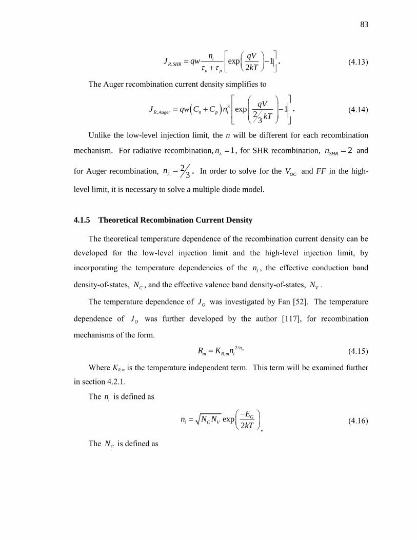
83
, exp 12
iR SHR
n p
n qVJ qw
kT. (4.13)
The Auger recombination current density simplifies to
3
, exp 12
3
R Auger n p i
qVJ qw C C n
kT. (4.14)
Unlike the low-level injection limit, the n will be different for each recombination
mechanism. For radiative recombination, 1 n , for SHR recombination, 2SHRn and
for Auger recombination, 23 n . In order to solve for the
OCV and FF in the high-
level limit, it is necessary to solve a multiple diode model.
4.1.5 Theoretical Recombination Current Density
The theoretical temperature dependence of the recombination current density can be
developed for the low-level injection limit and the high-level injection limit, by
incorporating the temperature dependencies of the in , the effective conduction band
density-of-states, CN , and the effective valence band density-of-states, VN .
The temperature dependence of OJ was investigated by Fan [52]. The temperature
dependence of OJ was further developed by the author [117], for recombination
mechanisms of the form.
2/
,mn
m R m iR K n
(4.15)
Where KR,m is the temperature independent term. This term will be examined further
in section 4.2.1.
The in is defined as
exp
2
Gi C V
En N N
kT
. (4.16)
The CN is defined as

84
3/2
*
22
2
nC
m kTN . (4.17)
The effective density-of-states effective mass for electrons, *
nm , varies slowly for
most semiconductors [92]. A coefficient term can be defined as
3/2
*
22
2
nC
m kK
,
(4.18)
and 3/2
CCN K T .
Likewise, the VN is defined as
3/2*
22
2
p
V
m kTN . (4.19)
The effective density-of-states effective mass for hole, *
pm , also varies slowly for
most semiconductors [92]. A coefficient term can be defined as
3/2
*
22
2
p
V
m kK
,
(4.20)
and 3/2
V VN K T .
The in with the KC and KV coefficient terms is
3/2 exp2
Gi C V
En K K T
kT
. (4.21)
A coefficient term for in can be defined, which combines the KC and KV coefficient
terms, i Cn VK K K , and the parameters contained in this term are
3
*3/2 *3/2
2
1
2in C V
kK m m
.
(4.22)
Finally the in with the inK coefficient term is
3/2 exp2i
Gi n
En K T
kT
. (4.23)

85
Combining Equations (4.3), (4.15) and (4.23) gives the general form of the
temperature dependent ,O mJ .
32
, , expm m
i
n n GO m R m n
m
EJ qwK K T
n kT
(4.24)
Where ,R mK is the OJ coefficient term for each recombination mechanism of the
form Equation (4.15).
4.1.5.1 Low-Level and High-Level Injection
In low-level injection the mn will be 1 for all three of the bulk recombination
mechanisms. The form of Equation (4.24) can be checked and the ,R mK can be found for
each recombination mechanism in the high-level injection limit.
The high-level injection saturation current density for radiative recombination can be
found by combining Equation (4.23) with the OJ from Equation (4.12).
2 3
, expi
GO Rad n
EJ qwBK T
kT
, (4.25)
The high-level injection saturation current density for radiative recombination which
matches Equation (4.24), with Radn equal to 1, is then
2 3
, , expi
GO Rad R Rad n
EJ qwK K T
kT
. (4.26)
And the ,R mK is the radiative recombination OJ coefficient term is ,R mK B .
The high-level injection saturation current density for SHR recombination can be
found by combining Equation (4.23) with the OJ from Equation (4.13).
32
, exp2
in G
O SHR
n p
qwK EJ T
kT
(4.27)
The high-level injection saturation current density for SHR recombination which
matches Equation (4.24), with SHRn equal to 2, is then

86
32
, , exp2i
GO SHR R SHR n
EJ qwK K T
kT
. (4.28)
And the ,R mK is the SHR recombination OJ coefficient term is ,
1R m
n p
K
The high-level injection saturation current density for Auger recombination can be
found by combining Equation (4.23) with the OJ from Equation (4.14).
9
3 2, ( ) exp
23
i
G
O Auger n p n
EJ qw C C K T
kT
(4.29)
The high-level injection saturation current density for Auger recombination which
matches Equation (4.24), with Augern equal to 2/3, is then
9
3 2, , exp
23
i
GO Auger R Auger n
EJ qwK K T
kT
.
(4.30)
And the ,R AugerK is the Auger recombination OJ coefficient term is
,R Auger n pK C C .
Therefore in high-level injection Equation (4.24) can be used for each of the bulk
recombination mechanisms, with the appropriate ,R mK and mn for each recombination
mechanism.
Identifying a method to estimate the GE over the simulated EG and OT will be
discussed in section 3.1.3.
4.2 Semiconductor Material Parameters
In order to solve for the terminal characteristics in the very high temperatures model
over a simulated EG and OT it is necessary to estimate the semiconductor material
parameters over these ranges. The material parameter fits described this section are used
in conjunction with these equations to estimate the ,R mJ values and the terminal
characteristics.

87
4.2.1 Intrinsic Carrier Concentration over Bandgap Fit
The most important material parameter needed in the very high temperatures model
is in . Not only is it in each of the ,R mJ equations, Equations (4.7) through Equation
(4.14), it varies by many orders of magnitude over both simulated GE and OT . Therefore
the temperature dependence and the multiplicative power of in in the ,R mJ equations are
very important to the overall temperature dependence of the model.
After carefully analyzing the in at 300 K for a wide range of semiconductor
materials over a large range of bandgap energies, it was determined that the direct and
indirect materials needed to have separate in fits, Figure 4.4.
In order to fit in over the simulated GE and OT , two different curve-fits were
evaluated. The first consisted of fitting the KC and KV coefficient terms over the
simulated GE . This method did not work well because of the large variability of *
nm and
*
pm for the direct bandgap and indirect bandgap materials over simulated bandgap,
Figure 4.2 [106].
Figure 4.2. Measured * /nm m and * /pm m for a wide
range of direct and indirect bandgap semiconductor materials [106].

88
The second fit consisted of fitting inK over simulated GE . This lead to a better fit
over simulated GE . The measured 3/2300inK for a wide range of direct and indirect
bandgap semiconductor materials are shown in Figure 4.3. Linear curve-fits for direct
bandgap and indirect bandgap materials are shown in Figure 4.3(a) with a log y axis and
Figure 4.3(b) with a linear y axis. The indirect bandgap fit becomes non-physical below
0.5 eV.
Figure 4.3. Measured 3/2300inK for a wide range of direct and indirect bandgap
semiconductor materials. Linear curve-fits for direct bandgap and indirect bandgap
materials [106]. The indirect bandgap fit becomes non-physical below 0.5 eV.
As shown in Figure 4.4, the in curve-fit for direct bandgap materials was a factor of
10 smaller than the in curve-fit for indirect bandgap materials, near the GaAs EG of 1.42
eV at 300 K [106].
- - - - - [eV] - - - - -

89
Figure 4.4. Measured in for a wide range of direct and indirect bandgap semiconductor
materials [106]. Linear curve-fits of 3/2300inK were used to predict the in for direct
bandgap and indirect bandgap materials. There is a factor of 10 difference between the
in curve-fit for direct bandgap materials and in curve-fit for indirect bandgap materials
Using the in curve-fit for indirect bandgap materials to calculate the ,R AugerJ for the
direct bandgap semiconductor GaAs in high-injection would lead to a recombination
current densities values that are 1000 times higher than the ,R AugerJ , calculated using the
measured in values for GaAs. The difference between the direct bandgap and indirect
bandgap in curve-fits is primary caused by the generally narrower conduction band
valley in direct bandgap materials, which generally lead to significantly smaller values of
*
nm , for direct bandgap materials. This causes the CN and in to be lower in direct
bandgap materials.
In order to assess the accuracy of the in curve-fits, the percentage difference between
the measured and curve-fit predicted values were plotted.
- -- - - - - [eV] - - - - - - - - - --
-
- -
- -
- -
- [1
/cm
3] -
- -
-
- -
- -
- -

90
Figure 4.5. The percentage difference between the measured and the linear curve-fit
predicted values.
The measured value of only one material, GaInP, was off by more than a factor of
two, which is acceptable for the purposes of the very high temperatures model.
To further validate the in curve-fits, they will be compared to material specific in
curve-fits, over a range of temperatures. The lines are the in curve-fits for direct
bandgap and indirect bandgap materials. The dots represent a variety of material specific
curve-fits for in over OT .
D
iffe
ren
ce
Be
twe
en
ni,fit a
nd
ni,data
[%
] d
- -- - - - - [eV] - - - - - - - -

91
Figure 4.6. Comparison of the in curve-fits with material specific in values at 300 K.
The lines show the in curve-fits for direct bandgap and indirect bandgap materials over a
range of OT .
The dots and the lines appear to match-up reasonably well for the wide range of GE
and OT . There also appears to be some variability in the measured data. For each
individual material the dots appear to be roughly the same distance above or below the
simulated line for each of the selected OT . The direct bandgap and indirect bandgap in
curve-fits could be further evaluated and improved by fitting the dots at each selected OT
separately and then relating the curve-fits over the range of OT .
The direct bandgap and indirect bandgap in curve-fits over a wide range of
simulated GE and OT have been describe in this section. These curve-fits are used in the
very high temperatures model. The recombination coefficients over simulated GE and
OT are still needed to calculate ,R mJ for each of the recombination mechanisms over
simulated GE and OT .
(a) Direct bandgap material (b) Indirect bandgap material

92
4.2.2 Recombination Coefficients
The recombination coefficients for radiative and Auger recombination over
simulated GE and OT are needed to calculate the terminal characteristics in the very high
temperatures model. These coefficients are material specific. The SHR lifetimes will be
calculated, which are needed to achieve the low-level injection limit and the high-level
injection limits valid.
4.2.2.1 Radiative recombination coefficients over bandgap fit
As will be shown later in section 4.3, the radiative recombination is limiting the
device performance in most of the very high temperatures model cases. The radiative
recombination coefficient is material specific and varies by material. It can also be
temperature dependent. The measured B values plotted in Figure 4.7, for both direct
bandgap materials and indirect bandgap materials. As expected, there is a large
difference between direct bandgap materials, shown as red squares, and indirect bandgap
materials, shown as blue diamonds. There is also a large amount of scatter in the B for
direct bandgap. Using III-V compound semiconductors it is possible to create materials
with the same EG and vary different element compositions.

93
Figure 4.7. The red squares are measured B values for direct bandgap materials. The blue
diamonds are measured B values for direct bandgap materials. Low, medium and high
lines have been developed to bracket the B for direct bandgap and indirect bandgap
materials.
Three fits have been developed for the radiative coefficients for direct bandgap and
indirect bandgap materials. These fits bracket the range of measured radiative
coefficients, with low, medium and high levels of radiative recombination. The direct
bandgap material fits are 4 orders of magnitude larger than the indirect bandgap material
fits. The direct bandgap material fits do not cover the full range of the B for direct
bandgap materials with a bandgap below 1 eV. In section 4.3 it will be shown that
materials below 1 eV do not perform well at higher temperatures.
Based on the data collected, it appears that the B may generally increase with
increased bandgap energy. Empirical fits could be developed to incorporate this increase.
The approach used with three ranges was deemed to be the most useful in the very high
temperatures model. The measured value of a real material can be matched to one of the
three ranges to predict the performance of that material.
The fits described in this section predicted the range of possible B over GE . In order
to calculate the very high temperatures model over a wide range of temperatures, it is also
important to know how the B varies with temperature.
(a) Direct bandgap material (b) Indirect bandgap material

94
4.2.2.2 Radiative recombination coefficients temperature dependence
A theoretical model for B was developed by Varshi [118, 119]. This model
predicted that the B of direct bandgap materials, GaAs, GaSb, InP, InAs and InSb would
decrease as the temperature increases. This model also predicted that the B of indirect
bandgap material Si would increase as the temperature increases. Early published
measurements indicated that it would increase, later measurements indicated that the B of
Si decreases as the temperature increases [120, 121]. The difference of the measured B
increasing and decreasing in Si is thought to be due to a difference in the in value and the
absorption data, which is affected by the emission of photons. Measurements of GaAs
indicate that the B increases as the temperature decreases [122], this has also been found
in GaAs quantum wells [123].
Based on the measured data it is possible that B could increase for some materials
and decrease for others as the temperature increases. Furthermore, very little is known
about the B for all of these materials above 200 °C, so any temperature dependence would
be extrapolated far from the measurements. It was determined that the best option was to
not vary the B over OT . If there is a general trend that B decreases as the temperature
increases then the very high temperatures model will somewhat under predict the
performance of these devices at higher temperatures.
The B value measured in literature is typically for the bulk material, factors such as
photon recycling will reduce the effective B [124]. If the B is reduced due to the
changing temperature or photon recycling by a factor of 10, the low B fit results could be
used for a material which has a bulk medium B at room temperature.
4.2.2.3 Comparing radiative recombination saturation current density
Many attempts have been made to create a saturation current fit to predict the quality
of solar cells. These fits have been referred to as state-of-the-art or empirical fits.
Without being able to quantify the B over EG these models are often based on empirical
data [87] or voltage shifted [84] from the junction bandgap. As the solar cell device

95
performance improves, solar cells have [125] and will continue to past these empirical
fits.
By using the B fits developed over EG in Section 4.2.2.1, it is possible to predict the
lowest possible ,OJ that can be achieved for a semiconductor material with the low,
medium or high values for B. Since the Shockley - Queisser detailed balance limit has
the same n, as Equation (4.7) and Equation (4.12), it can also be plotted for reference.
This is particularly useful for predicting the performance of direct bandgap materials,
which have high SHR lifetimes, since the Auger recombination will be small in a direct
bandgap material, and these devices will be limited by the radiative recombination.
Figure 4.8(a) shows the ,OJ for the radiative recombination in direct and indirect
materials. Figure 4.8(b) shows the ratio of the reverse saturation divided by the Shockley
- Queisser detail balance limited current for each of the radiative recombination cases.
The red dot below the solid blue line, was fabricated by Alta Devices [47]. This solar
cell has a very good back reflector and photon recycling. It is only a factor of ten larger
then Shockley – Queisser detail balance limit, solid black line. This red dot falls below
the solid blue line, which is the calculated saturation current based on the bulk low
radiative recombination coefficient fit for measured direct bandgap materials. This
shows that the actual ,OJ , due to radiative recombination, can be significantly lower than
the value predicted by measurements of the bulk materials [126].

96
Figure 4.8. The solid black line is the Shockley – Queisser detailed balance limit. The
red dots are the estimated ,OJ for measured solar cells. The blue lines are the
,OJ
predicted by the model for direct bandgap materials. The green lines are the ,OJ values
predicted by the model for indirect bandgap materials.
The ,OJ is estimated for the measured devices. This assumes that the radiative
recombination is limiting these solar cells. If other recombination mechanisms are
significantly affecting the performance of these devices, the radiative recombination will
be a smaller percentage of the total and the actual reverse saturation for the radiative
recombination would be smaller. This would move the red dots closer to the black line.
This would indicate that these solar cells have ,OJ values that are even better than the
plots indicate.
4.2.2.4 Auger recombination coefficients over bandgap fit
Just like the B, a fit for nC and pC is needed over GE and OT to calculate the very
high temperatures model. The Auger recombination is an important parameter for solar
cells constructed out of indirect bandgap materials, which are often 100 times thicker
than the direct bandgap solar cells. This causes the indirect bandgap solar cells to have a
significantly larger amount of Auger recombination.
(a) Saturation current density (a) Normalized saturation current density

97
Due to the fact that the measured nC and pC values were not available for all types
of materials, nC and pC values were combined to create the ambipolar Auger coefficient,
n pC C C . (4.31)
This parameter has been plotted for direct bandgap and indirect bandgap materials,
over a wide range of semiconductor types and EG, in Figure 4.9 [106, 127, 128].
Figure 4.9. The red squares are the measured C values for direct bandgap materials and
the blue diamonds are the measured C values for indirect bandgap materials.
The red squares are the measured C values for direct bandgap materials, and the blue
diamonds are the measured C values for indirect bandgap materials. There is a
significant amount of scatter in the measured values, which represent a wide range of
semiconductor materials, particularly in the compound III-V semiconductors where
material of different compositions can have same EG.
The measured values of C for low bandgap materials appear to reduce as EG
increases. This EG dependent decrease of the C has been fit by many [106, 129]. This is
likely caused by a decrease of the intraband Auger recombination [130]. The data point
with a bandgap energy of 3 eV and 1x10-34
cm6/s was extrapolated from the C values of
lower bandgap materials and is far below the measured values [106]. The reduction of

98
the C appears to stop for semiconductors with bandgap energies above 1 eV, and since
the bandgap above 1 eV are of interest in the very high temperatures model, the low,
medium and high Auger coefficient ranges have been chosen to bracket the measured
semiconductors materials above 1 eV. With the only exception being a InGaN, 3.0 eV,
measurement [128], which is much too high for a single junction solar cell.
4.2.2.5 Auger recombination coefficient over temperature
The measured C values of different semiconductor material have been shown in
literature to increase or decrease over temperature. The total Si Auger recombination
rates is often assumed to be [131]
0.5
301.4 10300
TC x
. (4.32)
The measured C value for Si increases as the temperature increases [132], while the
measured C value for SiC decreases as the temperature increases [133]. These measured
values appear to have significantly different slopes. In addition, three different
theoretical and empirical fits have been developed for Si over OT . These three fits lead to
very different results for C at high OT . The total GaAs C rate increases by an order of
magnitude, from ~10-30
[cm6/s] at 300 K to ~10
-29 [cm
6/s] at 500 K [134].
Because of the variability in the temperature dependence of C for different materials,
the Auger coefficient will not be varied over temperature in this model. In addition, it
will be shown in Section 4.3.2 that the temperature dependence of C will have little effect
on the results of the very high temperatures model for many of the cases considered.
4.2.3 Shockley Hall Read Recombination
The defects in the crystal lattice create energy states, which are in-between the
valance and conduction band. Recombination caused by these trap states is commonly
referred to as Shockley Hall Read recombination. This type of recombination depends

99
primarily on the quality of the material, which is related to the density of the defects. The
SHR lifetime is
1SHR
th Tv N
. (4.33)
Where σ is the trap capture cross section, thv is the thermal velocity and
TN is the
density of traps.
Due to the fact that SHR is dependent on the quality of the material and the number
of defects in the material, it will be improved as the growth method is improved.
Therefore, it does not have a fixed value like the radiative and Auger recombination
coefficients. It was decided that the best way to incorporate the SHR into these
calculations would be to compare it to the effective lifetime of the other two
recombination mechanisms. This value will be used to determine how small the SHR
lifetime can be before it increases the recombination.
An effective lifetime will be calculated for the radiative recombination and Auger
recombination mechanisms,
1 1 1
Eff Auger Rad
. (4.34)
Where Auger is the Auger recombination effective lifetime and Rad is the radiative
recombination effective lifetime.
In order to calculate the effective lifetime, the radiative effective lifetime and Auger
effective lifetime are needed.
4.2.3.1 Radiative recombination effective lifetime
There are different radiative recombination effective lifetimes for low-level injection
and for high-level injection. From Equation (4.12), the high-injection radiative
recombination effective lifetime is
1
exp( / 2 )Rad
iBn qV kT
(4.35)

100
When the material is in high-level injection, the calculated radiative recombination
effective lifetime is dependent on the bias voltage.
From Equation (4.7), in n-type materials the low-injection the radiative
recombination effective lifetimes is
1Rad
DBN
. (4.36)
From Equation (4.7), in p-type materials the low-injection the radiative
recombination effective lifetimes is
1Rad
ABN
. (4.37)
4.2.3.2 Auger effective lifetime
There are different Auger recombination effective lifetimes for low-level injection
and for high-level injection. From Equation (4.14), the high-injection the Auger
recombination effective lifetimes is
2
1
( ) exp( / )Auger
n p iC C n qV kT
.
(4.38)
As with the radiative effective lifetime, Equation (4.35), when the solar cell is in
high-level injection, the calculated Auger recombination effective lifetime is dependent
on the bias voltage.
From Equation (4.11), in n-type materials the low-injection the Auger recombination
effective lifetimes is
2
1Auger
p AC N
. (4.39)
From Equation (4.10), in p-type materials the low-injection the Auger recombination
effective lifetime is
2
1Auger
p DC N
. (4.40)

101
The Auger effective lifetimes and radiative effective lifetimes have been used in the
very high temperatures model to calculate an effective recombination lifetime. This
value can be used to determine if the SHR recombination will be comparable to the
Auger and radiative recombination in existing materials.
4.2.3.3 Carrier diffusion coefficient
In addition to calculating the Eff , the diffusion coefficient, D, has also been
calculated. The D can be calculated using the DL , and Eff .
D EffL D . (4.41)
LD can be used to determine if the low-level injection and high-level injection
assumptions are valid. For these assumptions to hold the DL
must be roughly 3 times
larger than the thickness of the solar cell.
3DL w (4.42)
The D can be found by equating Equation (4.41) and Equation (4.42) and solving for
D.
29
eff
wD
(4.43)
The carrier mobility can also be predicted using the Einstein relation
D kT (4.44)
In order for the low-level injection and high-level injection assumptions to remain
valid, the measured D of the chosen material must be less than or equal to the D predicted
by the very high temperatures model. For materials where the D is larger than the value
predicted by the model, the actual solar cell performance for that device can be found
using the measured D.

102
4.3 Analytical Simulations
This section contains the results of the very high temperatures analytical model. The
analytical expression and material parameter fits over EG and OT , described in this
chapter, were used to calculate the terminal characteristics of a solar cell over a wide
range of OT , over solar concentrations and for a variety of different materials. These
results can be used to identify the bandgap energy that produces the maximum
conversion efficiency for a range of selected temperatures.
4.3.1 Bandgap Optimization Over a Range of Temperatures
Due to the large number of possible material parameters combinations, a
representative case was chosen to illustrate terminal characteristic trends. A case with a
direct bandgap material in high-level injection, with medium radiative and medium
Auger recombination was chosen. A direct bandgap material was chosen because the
bandgap can be varied over a range of bandgaps and there are a variety of existing solar
cells. The medium radiative recombination material parameter fit was chosen because all
of the measurements were better than the medium fit and medium Auger recombination
material parameter fit was chosen because the direct bandgap material measurements
were close to this fit. The high-level injection assumption was chosen because solar cells
are often close to high-level injection in solar concentrators. In addition, the direct
bandgap devices were found to be strongly limited by radiative recombination, so there is
essentially no difference between the results calculated using high-level injection or low-
level injection, which have the same diode ideality factor.

103
Figure 4.10. The conversion efficiency predicted by the utlra high temperature model
over simulated bandgap energy for a wide range of selected temperatures. As the
temperature increases the saturation current density increases. This causes the conversion
efficiency to decrease. Also as the temperature increases the bandgap energy with the
highest conversion efficiency for a given temperature increases.
Solar cell system designers can chose a specific material system and then identify the
25 °C bandgap energy that would lead to the optimal bandgap energy at the chosen
energy.
As the temperature increases the saturation current density increases. This causes the
conversion efficiency to decrease. Also as the temperature increases the bandgap energy
with the highest conversion efficiency for a given temperature increases. Increasing the
temperature reduces both of these affects, thereby increasing the conversion efficiencies
(a) 1 sun concentration (b) 500 suns concentration
(c) 2000 suns concentration

104
at higher temperatures and reducing the peak bandgap energy. At 1 sun solar
concentration and 800 °C the RJ is larger than the SCJ for the simulated bandgap
energies below 1.75 eV. This results in a conversion efficiency that is essentially zero.
The peak conversion efficiency and corresponding simulated GE is plotted in Figure
4.13.
The main reason the conversion efficiency goes down so quickly as the temperature
increases is that the MPV and OCV are dropping. This decrease is caused by the rapid
increase of the RJ as the temperature increases. Figure 4.11 shows the OCV for the same
cases in Figure 3.13. As the temperature increases the OCV for the simulated GE
decreases. As the solar concentration increases the OCV increases and the rate of OCV
reduction decreases. The conversion efficiency is zero below 1.75 eV for 1 sun solar
concentration and 800 °C, because the RJ is larger than the SCJ for the simulated
bandgap energies which results in a MPV and a OCV that are essentially zero.
MPV

105
Figure 4.11. Open circuit voltage predicted by the very high temperatures model over
simulated GE for a wide range of selected temperatures. As the temperature increases the
OCV for the simulated GE decreases. Also, as the solar concentration increases the OCV
increases and the rate of OCV reduction decreases.
In addition to the conversion efficiency, an additional efficiency parameter, '
PV , was
calculated. This terminal characteristic is defined as the maximum power out divided by
the power above the simulated bandgap. It is useful when calculating the efficiency of a
system that includes additional elements, such as dichroic mirrors. This parameter has
temperature dependencies that are similar to the conversion efficiency. The main
difference is that this value does not approach zero as the bandgap energy increases.
(a) 1 sun concentration (b) 500 suns concentration
(c) 2000 suns concentration

106
Figure 4.12. The effective conversion efficiency, '
PV , predicted by the utlra high
temperature model over simulated GE for a wide range of selected temperatures. This
parameter has temperature dependencies that are similar to the conversion efficiency,
however it does not approach zero as the bandgap energy increases.
To further understand the connection between the peak conversion efficiency and the
operating temperature. The peak conversion efficiency was found for each of the
selected temperature and was then plotted with the associated values of EG, ηPV’ and f’ for
the peak efficiency. This provides a way to more carefully track these parameters as they
change over temperature. Figure 4.13 shows that the conversion efficiency decreases
smoothly as the temperature increases. It also shows that the EG increases as the
temperature increases. One part of the plot that is particularly interesting is temperature
regions over which the optimal EG does not changes very quickly. This can be seen in
the optimal EG between 200 °C and 400 °C at 2000 suns concentration. Here the EG is
(a) 1 sun concentration (b) 500 suns concentration
(c) 2000 suns concentration
(a) 1 sun concentration (b) 500 suns
(c) 2000 suns

107
essentially constant, whereas over the same range of temperatures, at 1 sun concentration,
the optimal EG changed by 0.3 eV. This temperature insensitivity is coming from the
gaps in the solar spectrum. This effect could be helpful when designing the complete
solar cell system, due to the fact that the solar cells can operate over a rather larger range
of temperatures and still be close to the optimum EG and peak power out over this range
of temperatures.
Figure 4.13. The optimal peak η, ηPV’, f’ and EG plotted for a wide range of selected
temperatures. As the temperature increases the optimal peak η decreases. In the 2000
suns cases the optimal EG changes very little between 200 °C and 400 °C.
(a) 1 sun concentration (b) 500 suns
concentration
(c) 2000 suns concentration

108
4.3.2 Conversion Efficiency over Operating Temperature
The plots in the other Sections of this Chapter are the simulation results for the case
with medium radiative recombination coefficient and medium Auger recombination
coefficient. This Section will evaluate what affect each recombination mechanism has on
the overall conversion efficiency.
The η for five different recombination limited cases is shown in Figure 4.14. In
these simulation the bandgap energy is 1.5 eV and it is held constant over temperature.
In each case the radiative recombination is not allowed to go below S-Q detailed-balance
limit. The first case shown in black is the S-Q detailed-balance limit. The second case
shown in red is for the case with low Auger recombination coefficient and the radiative
recombiantion equal to the S-Q detailed-balance limit. The third case shown in light blue
is the low Auger recombination coefficient and the low radiative recombination
coefficient limit. The fourth case shown in bark blue is for the case with high Auger
recombination coefficient and the radiative recombiantion equal to the S-Q detailed-
balance limit. The fifth case shown in light green is the low Auger recombination
coefficient and the low radiative recombination coefficient limit.
As in Figure 4.10, as the temperature increases the saturation current density
increases. This causes the conversion efficiency in each case to decrease. Also, as the
solar concentration increases the conversion efficiency increases. At 1 sun concentration,
the cases two and four are nearly identical to case one, which indicates that the Auger
recombination is insignificant at this concentration. At 2000 suns concentration, the case
two and case one are still nearly identical, and in case four the conversion efficiency is
now being limited by the high Auger recombination coefficient. This is still small
compared to case three and five, with low and high radiative recombination coefficients
repectively, which are clearly reducing the conversion efficiency more than the Auger
recombination.

109
Figure 4.14. The η simulated for five different recombination cases. At 1 sun the cases
with low and high Auger recombination coefficients and the radiative recombination
equal to the S-Q limit are nearly identical to the S-Q only limit, which indicates that the
Auger recombination is insignificant at this concentration. At 2000 suns the case with
only S-Q and low Auger recombination are still nearly identical, and the case with a high
Auger recombination coefficient and radiative recombination equal to the S-Q limit is
now reducing the conversion efficiency. This is still small compared to the cases with
low and high radiative recombination, which are clearly reducing the conversion
efficiency more than the Auger recombination.
This shows that the temperature dependence of the Auger recombination
coefficient is not important so long as it does not significantly increase the Auger
recombination coefficient above the high recombination coefficient limit.
(a) 1 sun concentration (b) 500 suns concentration
(c) 2000 suns concentration

110
4.3.3 The Peak Conversion Efficiency and Optimal Bandgap Energy Over
Temperatures and Solar Concentration
The temperature insensitivity of the optimal EG can be seen in more detail by plotting
the peak efficiency with more temperatures and solar concentration. The optimal
efficiency is plotted over temperature and concentration in Figure 4.15. It is plotted
assuming medium Auger recombination, medium radiative recombination, direct
bandgap materials and high-level injection. The optimal EG over the same range is
plotted in Figure 4.15 and Figure 4.16.
Figure 4.15. The optimal efficiency plotted over temperature and solar concentration. It
deceases as the temperature increases and the solar concentration decreases.
As expected from Figure 4.13, the conversion efficiency decreases smoothly as the
temperature increases and the solar concentration decreases.
A simple curve-fit of the conversion efficiency over temperatures and solar
concentration will be discussed in Section 4.3.5.

111
The optimal simulated EG plotted over temperature and concentration has more
structure then the optimal conversion efficiency. It increases as the operating
temperature increases and the solar concentration decreases.
Figure 4.16. The optimal EG plotted over temperature and solar concentation. The steps
are caused by the local maxima in Figure 4.10
The gaps in the solar spectra, Figure 3.6(a), cause local maxima in the conversion
efficiency over bandgap energy. This can be seen in the conversion efficiency over
bandgap energy plots, Figure 4.10. It is easy to see the local maxima in the conversion
efficiency at 25 °C. These local maxima in the conversion efficiency are caused by the
gaps in the solar spectrum and the conversion efficiency temperature coefficient, which
increases as the solar cell EG decreases.
As the temperature increases the conversion efficiency at lower simulated bandgap
energies decreases more quickly than the conversion efficiency at higher simulated
bandgap energies. This will cause the optimal bandgap to jump from one local maximum
to another local maximum at a higher bandgap as the temperature increases. This causes
the steps seen in the optimal bandgap energy over temperature and solar concentration.

112
These optimal EG transitions can be seen in Figure 4.17. The solid lines are the
conversion efficiency over the simulated EG for each of the plotted temperatures. The
black dots are the peak conversion efficiency for each of the temperatures. The arrows
shows the otpimal EG transitions between each temperature. As the OT increases from
394 °C to 395 °C there is a small change in the optimal EG, from 395 °C to 396 °C there is
no change in the optimal EG, and from 396 °C to 397 °C there is a large change in the
optimal EG. These large optimal EG transitions are causing the steps in Figure 4.16.
Figure 4.17. The lines are the conversion efficiency over EG at each of the temperatures.
The local maxima are caused by the gaps in the solar spectra. The black dots are the peak
conversion effiicency and optimal EG at each of the temperatures. The arrows shows the
otpimal EG transitions between each temperature. As the OT increases from 394 °C to
395 °C there is a small change in the optimal EG, from 395 °C to 396 °C there is no
change in the optimal EG, and from 396 °C to 397 °C there is a large change in the
optimal EG. These large optimal EG transitions are causing the steps in Figure 4.16.
The steps in displayed in Figure 4.16 can be seen in Figure 4.18(a) for selected
concentrations. There are large ranges of temperature over which the optimal EG is
constant. The fraction of energy in the spectrum above the optimal EG is shown in Figure
4.18(b).

113
Figure 4.18. (a) The optimal EG for selected concentrations over a range of temperatures.
The steps caused by the solar spectrum can clearly be seen. (b) The fraction of energy in
the spectrum above the optimal EG.
The steps in the optimal EG maybe be helpful from a system and solar cell design
standpoint since a chosen EG could be close to the optimal EG over a wide range of
temperature and solar concentrations. The EG of most real materials decreases as the OT
increases, so the optimal EG steps increase the range over which the EG of a real material
will be close to the optimal EG. If the optimal EG strictly monotonically increased, the
range over which the EG of a real material is close to the optimal EG would be smaller.
It will be shown in Section 4.3.4 that there is a range of bandgaps near the peak
conversion efficiency, which are less than few relative percent below the peak conversion
efficiency.
It would be beneficial to the system if the EG of the real solar cell remained constant
as the OT increased, and even better if it were designed to increase as the temperature
increased. It may be possible to counteract the temperature dependent EG narrowing, by
adjusting other physical properties which affect the EG, such as exerting pressure on the
solar cell [112] or by straining the junction layers. Clearly the reliability of these
approaches would need to be thoroughly investigated.
(a) Optimal bandgap energy (b) Fraction of incident light

114
4.3.4 Conversion Efficiency Over Temperature and Solar Concentration
The conversion efficiency plotted over temperature and solar concentration is helpful
in understanding how quickly the conversion efficiency decreases as the simulated EG
moves away from the optimal EG of the peak conversion efficiency at each temperature.
The conversion efficiency at 100 suns is plotted in Figure 4.19. Figure 4.19(a) is a corner
view and (b) is a top-down-view.

115
Figure 4.19. (a) is a corner view and (b) is a top-down view of the conversion efficiency
over temperature and bandgap energy at 100 suns concentration. These plots show how
quickly the conversion efficiency decreases for a given temperature from the optimal EG.
The conversion efficiency decreases as the bandgap increases and as the bandgap
decreases. These plots also show the peak conversion efficiency shifted to a higher
optimal EG as the temperature increases.
As shown in Figure 4.10, there is a optimal EG at the peak efficiency for each
temperature. For a paticular temperature the conversion efficiency of a simulted EG
above or below the optimal EG will be below the peak. Near the optimal EG this
difference will be small. Figure 4.20 shows the change of the conversion efficiency over
EG relative to the peak conversion efficiency at each temperature. The optimal EG is the
(a)
(b)

116
dark blue regions inside the navy blue regions. The flat portions of the optimal EG steps
can be seen when the dark blue peak conversion efficiency region remains constant over
a range of temperatures.
Despite the optimal EG steps, in this plot it is easier than Figure 4.19 to see that the
optimal EG is increasing as the temperature increases. For most materials the opposite is
true, the EG is decreases as the temperature increases. The optimal EG steps provide
regions where a material could match the optimal EG over a wider range of temperature,
more than would be possible if the optimal EG strictly monotonically increasing over the
entire range of temperatures.
Figure 4.20. The conversion efficiency over EG relative to the peak conversion efficiency
at each temperature. The four lines through the plot show the temperature dependent
bandgap narrowing of GaAs, CdTe, GaInP with a 25 °C bandgap of 1.6 eV and GaInP
with a 25 °C bandgap of 1.8 eV. At some temperatures, the range of EG with a
conversion efficiency less than 5% from the peak is fairly narrow, for other temperatures
this range is considerably wider. The optimal EG clearly increases as the temperature
increases.
(b) 500 suns concentration

117
The four lines show the temperature dependent bandgap narrowing of GaAs, CdTe,
GaInP with a 25 °C bandgap of 1.6 eV and GaInP with a 25 °C bandgap of 1.8 eV.
This plot shows that for some operating temperatures there a narrow range of
simulated EG that are less than 5% below the peak, such as 200 °C which has a EG range
that is only 100 meV range. While at other temperatures, the range of simulate EG within
5% is much wider, such as at 400 °C which has an EG range that is nearly 500 meV wide.
This range and the corresponding effect on the range of temperatures for which a given
EG is within 5% of the peak conversion efficiency at each temperature, is important for
optimizing the systems to generate the most energy over the expected range of operating
temperatures.
It would be preferable to find a high quality material with an EG range that will be
highly efficiency over the expected range of operating temperatures. GaAs covers the
range from 100 °C to 200 °C. The GaInP material with a 25 °C bandgap of 1.6 eV and
the CdTe bandgaps EG pass through the step face and therefore never quite reach the peak
conversion efficiency. If the system was being designed to operate at 275 °C to 325 °C, a
material with an EG of 1.38 eV at 300 °C, would likely be close to the ideal for that
system, which is between GaAs and GaInP with a 25 °C bandgap of 1.6 eV.
4.3.5 The Peak Conversion Efficiency Curve-fit Over Temperatures and Solar
Concentration
An easy to use curve-fit was developed to estimate the peak conversion efficiency
over the temperature and solar concentration range of interest. This curve-fit was used by
APRA-E to evaluate the potential of hybrid CPV and thermal concentrated solar power
CSP systems, sometimes referred to as hybrid CPV-T systems [24]. There are a wide
variety of possible CPV-T applications, ranging from small systems [135] to large utility
systems [136].
5 227.8732 1.8734 10 0.054662 1.3ln( )( , ) CC CT X T T X (4.45)
Figure 4.21(a) shows the peak conversion efficiency at 100, 300, 500 and 700 suns
from 100 °C to 600 °C. The solid lines are the results of the analytical model. The dots

118
are the results of the simple curve-fit, Equation (4.45). Figure 4.21(b) shows that the
absolute error between the analytical model and the simple curve-fit is less than 0.3
percentage points. Therefore the simple curve-fit can be used to give a first order
approximation of the peak conversion efficiency.
Figure 4.21. (a) The lines are the modeled conversion efficiencies over temperature at
each of the concentrations. The dots are estimated using the simple curve-fit. (b) The
absolute error between the results of the model and the curve-fit.
4.3.6 Multiple Junctions
Multiple junction solar cells can increase the overall conversion efficiency by
collecting photons more efficiently with more than one bandgap. Due to the higher
saturation current density at high temperature it may seem like there is little to be gained
from using a multiple junction device at high temperatures, however, due to the
exponential EG dependence of the saturation current density, there is potential to
significantly increase the conversion efficiency by using multiple junction devices.
To illustrate the possible conversion efficiency improvement a two junction three
terminal device was simulated over a range of possible top junction and bottom junction
bandgaps at 100 suns and 330 °C. The peak conversion efficiency for a tandem two
(a) (b)

119
junction solar cell device can be found by using a three terminal device, which does not
constrain the two tandem junctions to be current matched.
Figure 4.22. Simulated conversion efficiency over (a) top junction and bottom junction
EG, as well as, (b) bottom junction EG for a two junction three terminal tandem device
operating at 100 suns and 330 °C. The conversion efficiency peaks are caused by the
gaps in the solar spectrum.
The simulated conversion efficiency for a two junction three terminal tandem device
operating at 100 suns and 330 °C is plotted in Figure 4.22(a) over ranges of possible top
junction and bottom junction EG., Figure 4.22(b) shows the same simulation for a range
of possible bottom junction EG. The single junction efficiency for a 1.6 eV device at
330 °C is 17.3 %. The peak conversion efficiency for the two junction case under the
same conditions is 23.9%. As with the single junction case, the peaks in the conversion
efficiency are caused by the gaps in the solar spectrum.
In addition to the two junction tandem simulations, the peak conversion for
Shockley-Queisser detailed balance limit from 1 to 10 junctions was calculated over a
range of selected temperatures, Figure 4.23. The novel method used to quickly find the
(a) (b)
(a) (b)

120
global peak η of an independently connected multiple junction solar cell system, is
described in Appendix D.
Figure 4.23. The peak conversion for Shockley-Queisser detailed balance limit from 1 to
10 junctions calculated over a range of temperatures.
4.4 Additional Effects
The analytical model described in this chapter has focused on simulating solar cells
in ideal cases, the Shockley-Queisser detailed balance limit and various possible
recombination levels. While it may be possible to develop solar cells that reach or even
surpass these cases, there are also physical effects that can reduce the solar cells
performance below these cases. This section will only briefly examine some of the
important effects that could limit the solar cell when operating at high temperatures. It is
therefore important to consider these when choosing a material which can mitigate these
effects in this extreme operating temperature range. These effects should be studied in
more detail when developing and test solar cells. One material that may be a good choice
in this operating range is SiC. Functioning MOSFET SiC devices have been fabricated to
operate at 600 °C [137] and a SiC solar cell has been fabricated [83].
Some of these are internal effects, while others are 3-D effects that will not be
captured by 1-D analytical or numerical models. The effects can also be classified

121
according to whether they will appear immediately or whether they have a reliability
effect that will appear after the solar cell has operated for an extended period of time.
4.4.1 Internal Effects
The immediate internal affects include the temperature dependent decrease of the
mobility and the temperature dependent increase of the thermal velocity, which will
increase the SHR recombination. These types of losses can be identified by reviewing
the temperatures dependent material properties of a particular material. A numerical
model has used to study these internal material parameters in Chapter 6.
The internal reliability affects include: atom diffusion, defect migration and melting.
High temperature diffusion is a common method used to dope semiconductor materials.
These effects can slowly degrade the performance of the solar cell over time.
Sources of atom diffusion include: dopant atoms, intrinsic atoms from other
heterojunction layers, metal layers, passivation layers, anti-reflectant coating layers, and
the atmosphere/environment. The effect of atom diffusion would be difficult to
generalize in an analytical model because it is material dependent [138], device structure
dependent, varies for each atom inside of each semiconductor material and is spatially
dependent. At 600 °C an unprotected Si solar cell could fully oxidize. One way to limit
the oxide growth would be to encapsulate the solar cell. Another method would be to
seal the solar cell inside of a container, which had an oxygen free environment. This
container could be filled with Nitrogen.
The melting point for various indirect bandgap and direct bandgap materials are
shown in Figure 4.24. The melting points for materials above 1 eV are well above
600 °C.
For many reliability reasons it is important to operate the solar cell well below the
melting point of the semiconductor layers. The melting point is above 1000 °C for
semiconductors above 1 eV. The upper end of the temperature range chosen, 800 °C, is
close to the melting point of semiconductors in the EG range of interest.
Not only is it important to identify the operating temperature, or average
temperature, it is even more important to identify the region which could experience

122
localized heating. This heating could be caused by current crowding and joule loss, it
could be caused by defects in the semiconductor material, or it could be caused by non-
uniform illumination of the solar cell.
Figure 4.24. Melting points for indirect bandgap and direct bandgap materials over the
bandgap range of interest.
4.4.2 External and 3-D Effects
There are many other temperature dependent mechanisms that could hinder the
temperature dependent performance; one of these is the temperature dependent increase
of the resistivity in the emitter and metal layers. This will be discussed in more detail in
Chapter 5.
Some of the 3-D reliability effects include delamination of adhesives, thermal
expansion, UV degradation of optical elements, expansion of trapped gases, and thermal
acceleration of room temperature reliability effects.

123
4.5 Summary and Conclusions
While a high performance high temperature solar cell may not exist today, that does
not limit the possibility of such a device being developed in the future. The
recombination limited cases analyzed in this chapter indicate that it is possible to develop
a high performance solar cell at much higher OT than are currently being developed. In
addition, this chapter identified parameters such as the optimal EG that will be strongly
affected by the OT .
In order to simulate the recombination limited cases over a broad range of operating
temperatures and bandgap energies, novel curve-fits were developed to calculate the
material parameters in , B and C over these ranges. Because the temperature dependence
of B and C was found to be material dependent, these parameters were held constant over
temperature. The recombination limited cases are necessary in the initial design phase to
quickly simulate the potential of solar cell operating over a broad range of OT and EG.
The temperature dependent of B and C can be used after a candidate material has been
chosen.
The results of this work showed that the simulated recombination limited η of direct
bandgap solar cells operating at temperatures above 300 °C can be significantly higher
than previously estimated [83]. In the case were B=1x10⁻⁹
cm3/s, C=1x10-30 cm
6/s and
SHR is significantly smaller than the Eff of the other two recombination mechanisms, the
300 °C peak η at 500 suns could be over 20% and at 2000 suns over 22%, with an optimal
peak EG of 1.8 eV in both cases.
The η of a tandem two junction devices were analyzed to evaluate the potential of
using multiple junction solar cells at high temperatures. The three terminal simulations
showed that the peak conversion efficiency of a tandem two junction device can be over
35% higher than the peak single junction device at the same temperature.
Based on these simulations it appears that the conversion efficiency of an
appropriately designed solar cell operating above 300 °C could be quite high. These solar
cells could be very useful in high temperature applications. Chapter 5 will show the

124
importance of considering the OT when optimizing the grid electrodes of the 3-D solar
cell. Chapter 6 will show that it is possible to match the temperature dependent terminal
characteristics using detailed numerical models.
4.5.1 Future Work
The calculations in this chapter assume that 100% of the photons above the
simulated GE are absorbed and converted to current. This is useful for determining the
upper limit of the SCJ , for devices that do not absorb photons below the bandgap energy.
This model could be extended by including realistic partial absorption for direct and
indirect bandgap materials [114, 139]. Doing this will likely change the optimal peak EG
by a few tens of millivolts. It would also allow the thickness of the solar cell to be
studied. Thinning the solar cell will reduce the photogenerated current, and it will also
reduce the volume over which th bulk recombination can occur. The optimal thickness
could be found, by varying the thickness at each temperature.
The of semiconductors are strongly influenced by the OT . This has been
measured for the direct bandgap material, such as GaAs, over a wide range of photon
energies [101] and near the band edge [115]. Therefore it will likely be necessary to
include the temperature dependent optical bandgap narrowing in the absorption model,
when optimizing the device thickness. In addition to being temperature dependence, the
of semiconductor materials is also doping dependent. However, this dependence
is not the same for all materials or dopants. For p-type GaAs the measured
changes very little as the doping concentration increases from 2x10¹⁷
[cm-3
] to 1.2x10¹⁸
[cm-3
], and for n-type GaAs the measured varies from that of a direct bandgap
material, to an absorption coefficient that is more similar to an indirect bandgap material
[116].

125
5. TEMPERATURE DEPENDENT RESISTIVE LOSSES
The goal of Chapter 4 was to estimate the conversion efficiency for a variety of
recombination limited cases. This allowed the model to simulate the maximum possible
conversion efficiency that could be reached in each case. This model assumed that the
solar cell can be designed so that all other loss mechanisms are negligible. However, in
practice it is not possible to completely eliminate all of the other loss mechanisms, many
of which arise from the 3-D structure of the solar cell. One important 3-D loss
mechanism that can significantly affect the performance of a solar cell is the resistive
loss.
This Chapter will examine how the total external Rseries can significantly affect the
temperature dependent solar cell performance. This is found to be even more important
when operating solar cells at higher temperatures. As the solar cell temperature
increases, the resistivity of most materials also increase. Therefore it is important to
consider the resistive losses at the expected operating temperature when optimizing a
solar cell design.
The results of the quasi 3-D distributed emitter model described in this chapter can
be used in conjunction with analytically solar cell models, Chapter 4, as well as detailed
numerical solar cell models, Chapter 6. The focus will be the OT range of terrestrial CPV
solar cells. It is expected that the resistive losses will be even more significant, over the
temperature range explored in Chapter 4.
It is not possible to completely eliminate the resistivity in materials that are not super
conducting. Common sources of series resistance are the Lateral Conducting Layers
(LCL), the metal semiconductor contacts, the grid electrodes, the busbar electrodes and
the semiconductor bulk. The grid electrodes and LCL are typically optimized to produce
the largest possible conversion efficiency, by limiting the overall resistivity of the solar

126
cells, while balancing other losses, such as the shadowing caused by the electrodes and
the optical loss caused by the LCL. This is particularly important in solar cells which
have very thin LCL, which can lead to high values of sheet resistance, Rsheet. For
materials with low enough Rsheet in the emitter layer will act as the LCL. In some cases
the Rsheet can be reduced by adding a semiconductor window layer on top of the emitter
layer. For solar cell materials with a high Rsheet in the emitter, a transparent conducting
layer (TCL) is often added. Common TCL used on solar cells include Indium Tin Oxide
(ITO) and Aluminum Zinc Oxide (AZO).
A wide variety of grid geometries and patterns have been examined !Flat, 1979
#623;Moore, 1979 #624?. Many different approaches have been implemented by others
to quantify and reduce the resistive losses. One common approach is to fabricate a large
number of test devices. Another common approach is to use a simple analytical model,
often in 1-D. More recently, a variety of quasi-2D and quasi-3D models have been used.
Each of these approaches has some benefits and limitations, and will be discussed in
more detail. They are often used in combinations to take advantage of the benefits of
each approach and diminish the associated limitations.
One of the most common approaches to reduce the resistive losses is empirical; it
involves fabricating a large number of devices with different design parameters, such as
changing the number of grid electrodes, GN , their spacing, their width and their
thickness. Other design parameters that can be varied include the busbar thickness, the
thicknesses of the LCL and doping of the semiconductor LCL. The performance of these
devices is then measured and the optimal design is identified. This approach to quantify
and optimize the grid electrode and busbar electrode design is limited by a number of
factors. First, the fabrication variations can significantly affect the uncertain and
variability of the measurements. Second, the gird electrode patterns that will be tested
are limited by the predefined mask. Third, the number of device parameters that can be
varied are limited by the number of test solar cells that can be fabricated. Fourth, the
device parameters to be tested are limited by the fabrication technology, therefore it is not
possible to test what will happen if a device parameter is changed or improved beyond
the capabilities of the current fabrication processes. Lastly, the fabrication and

127
characterization of a large number of devices can be a slow and time consuming process.
Despite the many draw backs to the empirical approach, it is often used to optimize the
grid electrode and busbar electrode pattern. The results from these measurements are
often used to develop analytical and quasi-3D models.
Another common approach to analyze the resistivity losses is to use a simple
analytical model. These analytical models can be 1-D and 2-D. Wolf was among the
first to study series resistance in a solar cell in 1963 [140]. The model he developed
included an equivalent resistance, which was calculated using the measured Rsheet. Later
Wyeth developed an analytical model using the power loss [141]. Since then a number of
quasi-2D models have been developed [142], these models are limited to 1-D current
flow in the LCL.
A more advanced quasi-3D numerical model has been developed by Haas [143].
This model could quantify the bias-point loss and did not limit the current flow through
the LCL to 1-D. The bias-point loss is caused by the voltage drop across the LCL which
causes parts of the solar cell to operate away from the intrinsic maximum power point of
the solar cell.
The work described in this chapter extends the quasi-3D model developed by Haas,
by adding temperature dependent material parameters into this model. This allows the
effect of temperature on the terminal characteristics to be quantified.1
The temperature coefficient of the 3-D solar cell will be affected by the front-surface
grid electrode pattern and the LCL. There are many important trade-offs in optimizing
the grid electrodes. These include the minority carrier lifetime in the emitter and the grid
electrode shadowing. If the emitter is too thick, more than 1/3 the diffusion length, the
carriers will not be efficiently collected, which will decrease the SCJ and the η of the
device. Increasing the GN will decrease the resistivity, which will reduce resistive
1 Sections 5.1 through 5.6 are based on the paper “A distributed emitter model for solar
cells: Extracting a temperature dependent lumped series resistance” by J. R. Wilcox and
J. L. Gray, which was published in the Photovoltaic Specialists Conference (PVSC)
proceedings, 2012 38th
IEEE (Wilcox, 2012 #544). ©2012 IEEE.

128
losses, however, it will also increase shadowing, which will decrease the SCJ , which will
also decrease the η.
Figure 5.1. (a) Top and (b) corner view of the typical comb shaped grid and busbar
electrodes on the emitter of a generic solar cell. The thick black line is the busbar and the
thin black lines are the grid electodes. The area between two grid electrodes is a tile and
the area between a grid electrode and the dashed line in (b) is a half-tile. The pink region
is the emitter layer and the light blue region is the absorber layer. The gray arrows and
lines indicate the current flow within the device (after [144] © 2012 IEEE).
There are a number of resistive losses in solar cells. Figure 5.1(a) shows the grid and
busbar electrode pattern of a generic solar cell. This figure is not to scale. Here, Bl is the
length of the busbar, Gl is the length of the grid lines, Tw is width of a tile, and Et is the
emitter layer thickness. The area between grid electrodes will be defined as a tile. In
Figure 5.1(b), the area between a grid electrode and the dashed lined is defined as a half-
tile. The gray arrows and lines indicate the flow of current out of the absorber layer into
the pink emitter layer, the current then flows laterally into the grid electrodes and on to
the busbar electrode.
There are a variety of resistive losses in a typical solar cell, these include back
conductor joule loss, the back contact joule loss, the internal joule loss, the bias-point
loss, the emitter joule loss, the front contact joule loss, the front grid electrode loss and
the front busbar joule loss.
(a) Top view (b) Corner view

129
In most solar cells, the back conductor can be designed so that the resistive losses are
negligible. The back contact resistance is often small, and must be balanced with the
surface recombination caused by the back contacts. Because the carrier lifetime
necessitates the solar cells to be very thin, on the order of a few microns for direct
bandgap materials and tens to hundreds of microns for indirect bandgap materials, the
internal joule loss from the back to the front is typically negligible.
The LCL, front contact resistance, front grid electrodes, and front busbar, must be
optimized together to achieve the highest possible solar cell η. Increasing the thickness
of the emitter will reduce the resistivity, while at the same time it will increase the
recombination of carriers in the emitter. Increasing the number and width of grid
electrodes will reduce the resistance between the emitter and the busbar. It will also
increase the shadowing, which will reduce the photons that enter the solar cell and
thereby reduce the photo generated current. If the busbar is over the active regions of the
solar cell, as the width is increased, the shadowing will also increase.
It is relatively straight forward to calculate the components of the effective SeriesR
caused by joule losses. In order to determine additional effective SeriesR components such
as bias point loss, it is necessary to model the 3-D structure of the solar cell. The bias-
point loss was carefully quantified by Haas [143]. This loss is caused by the resistance in
the front surface and to a lesser extent in the back surface. Because the resistance causes
a voltage drop across the surfaces of the solar cell, not all of the solar cell can operate at
the intrinsic optimal max power point for the solar cell junction. Large regions of the
solar cells will be forced to operate away from the intrinsic max power voltage. Areas
close to the contact pads will operate at voltages below the optimal max power point and
the regions in-between the grid electrodes will operate at higher voltages. The regions of
the solar cell that operate away from the intrinsic max power point, contribute to the bias-
point loss. The extrinsic max power point of the 3-D solar cell is found by adjusting the
terminal voltage near the intrinsic max power voltage until the peak extrinsic output
power is located.

130
5.1 Series Resistance Losses
As the operating temperature increases, nearly all of the series resistance losses in
the solar cell will increase. In this model the effect of each of these losses will be
summed to find the total equivalent series resistance, TR .
T B G C L A RR R R R R R R (5.1)
Here the busbar resistance, BR , is defined to include any resistive loss from the
terminal contact pad to the grid electrodes. The grid electrode resistance, GR , includes
the resistive losses caused by the grid electrodes. The contact resistance, CR , includes
the resistive losses between the gird electrodes and the front LCL. The resistance of the
front LCL, LR , accounts for the resistive losses inside of the TCL and emitter layers.
Any resistive losses between the emitter and the back contact are included in the
semiconductor resistance, RA. And the resistive losses between the semiconductor and
the back contact pad are included in, back LCL resistance, RR .
Some types of solar cells may have additional components, specific to that type of
solar cell. These might include additional solar cell junctions or unique structures
specific to that type of solar cell.
The resistive losses caused by each component of TR can be found by using the
quasi-3D model. In the quasi-3D model, each tile is broken up into very small vertical
elements which connect to the front LCL and the back LCL of the solar cell. The LCL
connects to the grid electrodes, which connect to the busbar electrode, and then to the
terminal contact pads. Each vertical element in the quasi-3D model is simulated as an
intrinsic solar cell. Measured values of the resistance are used to simulate the 2-D LCL
and the electrodes.
5.2 Temperature Dependent Non-Ideal Diode Parameters
Many different types of solar cell models can be used to simulate the 1-D
characteristics of the intrinsic solar cell elements. These models can range from

131
measured J-V data to a simple diode equation all the way up to the simulation results of a
complete detailed numerical model.
A simple diode model such a non-ideal diode equation (Equation (3.6)) can be used
during the development stage to provide useful insight into the effect that temperature has
on the TR . The extrinsic non-ideal diode equation is,
exp 1
Series SeriesSC O
O Shunt
q V JR V JRJ J J
nkT R
. (5.2)
This entire equation can be used to simulate the characteristics of a solar cell
element, if the ShuntR of a particular material is low or the SeriesR of the solar cell element
is high. However, for high quality solar cells, ShuntR is high and SeriesR is low. In this
Chapter the ShuntR of the solar cell element is assumed to ∞. Since most of the SeriesR
comes from the front LCL and back LCL, it will be assumed that the series resistance of
the solar cell element is 0. This gives the intrinsic non-ideal diode equation,
exp 1SC O
O
qVJ J J
nkT
. (5.3)
The results of the quasi-3D simulations can be used during the initial development
stage. A detailed numerical model of the solar cell could later be used to more carefully
simulate the characteristics of the solar cell elements, which would allow the resistive
losses to be refined, which could be used to further optimize the solar cell design.
In this chapter, the intrinsic non-ideal diode equation will be used inside of the quasi-
3D numerical model to simulate the solar cell junction at each point across the solar cell.
The quasi-3D model will then be used to numerically solve for the extrinsic max power
point of the entire 3-D solar cell. The numerical solution contains the voltage bias point
for each of the solar cell elements simulated. These voltage bias points can be used to
estimate the bias-point loss and each form of joule loss. The resistance terms in Equation
(5.1) can be extracted from these power losses.
The simple extrinsic non-ideal diode Equation (5.2) can be used to fit the J-V
characteristics of the quasi-3D distributed emitter simulations. However, due to the 3-D

132
resistive effects simulated, the J-V curve modeled by the extrinsic non-ideal diode
equation will only match the quasi-3D J-V curve at the SCJ , PM and OCV points.
In order to simulate the intrinsic non-ideal diode elements over a range of OT , the
values of SCJ , OJ and n over this range are needed. For the purposes of this broad study,
it will be assumed that n=1 over the range of OT . The n of real devices can change over
OT if the dominate recombination mechanism changes.
5.2.1 Temperature Dependent SC
J
As described in Section 3.1.3, generally as the OT increases, the EG deceases, this
will cause the SCJ of a typical solar cell to increase. However, there are many other
affects that will influence the SCJ . The bandgap of the absorbing material will decease as
the temperature increases, this will typical cause the SCJ of the solar cell to increase.
However, if this occurs in a region of the solar spectrum where the solar irradiance is
zero due to absorption in the atmosphere, the SCJ will not increase. This can also happen
if optical elements such as a dichroic or filter are limiting the photons in the solar
spectrum just below the bandgap energy. Another way in which the SCJ of one solar cell
can be restrained from changing as the temperature increases is when more than one solar
cell junction is in series, and another solar cell junction is limiting the SCJ of the series
connected tandem. In addition, the SCJ can be affected by the internal parameters of the
devices, such as the material lifetime which can decrease the SCJ as the temperature
increases. The SCJ can also be reduced by the passivation, window or emitter layers on
the front of the solar cell. The bandgaps of these layers will decrease as the temperature
increases; this can reduce the high energy photons collected by the solar cell, which will
cause the SCJ to decrease.
Because the SCJ can increase or decrease as the temperature increases, it will be held
constant when calculating the distributed emitter resistance in this Chapter. Since the

133
SCJ of an unrestricted GaAs solar cell will increase less than 5% over this range of OT ,
resistive losses estimated by the quasi-3D will not change significantly over this range of
temperatures. For this study a SCJ value of 1500 mA/cm2 was chosen. This is
approximately the SCJ of a GaInP/GaAs tandem solar cell at 100 suns [145] or a single
GaAs solar cell at 50 suns [125].
5.2.2 Temperature Dependent O
J
The OJ will increase when the temperature increases or the bandgap energy
decreases. A temperature dependent OJ which includes the temperature dependence of
EG is needed to calculate the temperature dependent terminal characteristic for the solar
cell elements in the quasi-3D model.
A generalized form of the temperature dependence of OJ , developed by the author
was described in Section 4.1.5. For the common recombination mechanisms radiative,
SHR and Auger the generalized form is shown in Equation (4.24), which can be used for
low-level and high-level injection. This model is useful to estimate the recombination
limits, however, it was not possible to include the EG dependence, due to the wide
variation of EG over temperature for various materials. Therefore, a curve-fit method for
estimating the OJ over a range of EG and a short range of OT was developed by the
author [144]. This method which will be described below and in more detail in Appendix
B.2, will be used to estimate the OJ . This curve-fit method is particularly useful because
the temperature dependent OJ with bandgap narrowing can be found using the EG at 300
K, ,300G KE
2.
2 Based on the paper “Estimating saturation current based on junction temperature and
bandgap” by J. R. Wilcox A. W. Haas, J. L. Gray and R. J. Schwartz, which was
published in the 7th
International Conference on Concentrating Photovoltaic Systems,
2011 (Wilcox, 2011 #99). ©2011 PSE AG

134
Because the OJ depends on EG, and the temperature dependent bandgap narrowing is
material dependent, a generic temperature dependent fit was created to approximate the
OJ over simulated material bandgap energy and temperature.
,300 ,300, 300 ,O O OG K G KJ T K J EKE , (5.4)
where ,300'* 'G KO EK exp S I . (5.5)
The S’ and I’ are temperature dependent polynomials which account for the
temperature dependence of EG and the OJ .
Table 5.1
Temperature dependent OJ curve-fit model S’ coefficients (after [104] © 2011 PSE AG).
Coefficient Value
A0 -145
A1 1.17
A3 3.72x10⁻³
A4 5.91x10⁻⁶
A5 -3.76x10⁻⁹
Table 5.2
Temperature dependent OJ curve-fit model I’ coefficients (after [104] © 2011 PSE AG).
Coefficient Value
B0 -24.587
B1 1.79x10⁻¹
B3 5.19x10⁻⁴
B4 7.97x10⁻¹⁰
B5 -4.97x10⁻¹⁰

135
This equation can be used with any ,300(300 , )O G KJ K E that has been evaluated at 300
K. In this chapter, the state-of-the-art OJ model developed by Gray was used [87].
The development of this curve-fit method is described in Appendix B.2. The validity
of this method was checked by comparing the OJ estimated using this method, with the
OJ calculated using the temperature dependent EG narrowing of the measured materials
plotted in Figure B.2(a) and Figure 5.2(a). Figure 5.2(b) shows that the OCV calculated
using this method and material specific OJ are off by less than ½kT at 350 K.
Figure 5.2. (a) Reverse saturation current density over bandgap for three of the eight
temperatures modeled. (b) Comparison of the pseudo-data OCV over temperature and the
values calculated using the polynomial slope and intercept OJ (T,EG(300 K)) curve-fit
(after [104] © 2011 PSE AG).
5.3 Temperature Dependent Resistance
The resistance of most metals, TCL and semiconductors increase as the temperature
increases. This can lead to significant resistive losses. It is therefore important to
consider the range of possible operating temperatures when designing the resistive layers.
(a) (b)

136
A big source of resistance in most solar cells is the TCL and emitter layer SheetR .
Typically these layers must be thin to limit others losses, such as carrier recombination
absorption.
Due to the thinness of these layers, the temperature dependent change of the tE will
not change significantly. This will be discussed more in Section 6.3.1. In this chapter tE
will be held constant. Near room temperature the dopants will be nearly fully ionized, so
A AN N or D DN N . On the other hand, the mobility of most semiconductors will
decrease to the power, γ. This will be discussed in more detail in the following section.
The SheetR of a TCL will be similar.
5.3.1 Temperature Dependent Lateral Sheet Resistance
The mobility of most semiconductors are sensitive to the temperature, free carrier
concentration, doping density and the electrical field inside the semiconductor. These
dependencies for Si will be explored in more detail in Section 6.6.
The SheetR can cause a significant voltage drop to occur as current transverses
laterally through these layers. The SheetR due to both carrier types is
1sheet
n p
Rq nt q pt
, (5.6)
where n is the electron mobility, p is the hole mobility and tE is the emitter thickness.
The current flow in a semiconductor will often be dominated by the majority carrier. At
the max-power point of a solar cell the minor carrier concentration can be significant.
High quality solar cells and concentrator solar cells can have high minor carrier
concentrations.
When nn is significantly larger than p p the SheetR simplifies to,
1
sheet
n
Rq nt
(5.7)
When p p is significantly larger than nn the SheetR simplifies to,

137
1
sheet
p
Rq pt
(5.8)
In this chapter, the other dependent parameters held constant, the mobility can be fit
over temperature.
O
M
T
T
(5.9)
The temperature dependent slope of the mobility, , can be found by fitting
measured data. When a semiconductor is heavily doped, which is typical of solar cell
emitter layers, will decrease (Section 6.6). It will also be reduced when the free
carrier concentration is high and when the electric field is high.
The intrinsic values for common semiconductor materials at 25 °C are displayed
in Table 5.3, the typical values range from -3 to 0.
Table 5.3
The intrinsic values for common semiconductors at 300K (after [144] ©2012 IEEE).
n-type p-type
Si γ -2.42 [146] -2.20 [146]
GaAs γ -1.0 [147] -2.1 [147]
Ge γ -1.66 [148] -2.33 [149]
GaP γ -1.7 [150] -2.3 [150]
The temperature dependent conducting layer sheet resistance can be found by
substituting Equation (5.7) into Equation (5.9).
, M
MSheet Sheet T
O
TR R
T
(5.10)
Due to the wide range of possible values, the front LCL SheetR will be calculated
over OT for a selected range of values from -3 to 0. Figure 5.3 shows LCL SheetR as a

138
percent change relative to the LCL SheetR at 25 °C. When the value of a
semiconductor is 0, the SheetR will not change as the temperature increases. When the
value is -3, the SheetR will increase nearly 100% between 25 °C and 100 °C.
Figure 5.3. The temperature dependent LCL SheetR change compared to the LCL SheetR at
25 °C, for a selected range of the temperature dependent mobility factor, . As
decreases the SheetR above 25 °C increases. For a value of -3, the SheetR can increase
nearly 100% at 100 °C (after [144] ©2012 IEEE).
The SheetR not only causes the joule loss in the LCL to increase, it will also cause the
bias-point loss of the LCL to increase. This effect will be explored further in Section 5.4.
5.3.2 Temperature Dependent Metal Resistivity
The resistivity of most metals increase as the temperature increases. To the first
order the temperature dependences of the metal resistivity is given by
,25 [1 ( 25 )]M M C T C (5.11)

139
As the temperature increases, M , varies according to the temperature dependent
metal resistivity coefficient, . Most of the metals commonly used in solar cell
electrodes have values that are around 0.004 K
-1. Therefore the resistivity of the
solar cell electrodes increase as the temperature increases 26 % as the temperature is
raised from 25 °C to 100 °C. The percent change of M is plotted in Figure 5.4, for
values ranging from 0 K-1
to 0.008 K-1
.
Figure 5.4. The temperature dependent change of the metal resistivity, M , compared to
M at 25 °C, for a selected range of the temperature dependent metal resistivity
coefficient, . As increases, the M above 25 °C increases. For an value of
0.008 K-1
, the M can increase nearly 60% at 100 °C (after [144] ©2012 IEEE).
5.4 Temperature Dependence of the Equivalent Series Resistance
The next step is to calculate the equivalent series resistance, eqR , of the conductor
layer. The eqR can account for all of the resistive losses in the LCL, such as the LCL
joule losses and the biasing-point loss. The LCL joule losses can be estimated
analytically for a half tile [143].
ρM

140
3 2
Sheet Teq
G
R wR
l
(5.12)
The analytical solution does not account for bias-point loss, and will therefore be a
better approximation at lower temperatures, when SheetR is small or the absolute value of
γ is small. It will be calculated over a range of temperatures and compared to the quasi-
3D numerical model for SheetR = 100 Ω/ and
SheetR = 500 Ω/, for γ = -0.5, -1.5 and -
2.5, Figure 5.5.
The eqR will be extracted from the quasi-3D numerical model, using a method
developed by Haas [143]. This method uses the power loss due to the bias-point loss,
,L BPP , and the front LCL joule loss, ,L CJP , along with the max-power current modeled to
find eqR .
, ,
2 2
L BP L CJ G
eq
MP T
P P lR
J A
(5.13)
In order for this expression to be valid, the extrinsic MPJ must be close to the
intrinsic lossless MPJ . Simulations with more than a 1 % difference will not be included
in the plotted data. The eqR is simulated using the quasi-3D model for 25 °C, 50 °C,
75 °C and 100 °C. In addition the 25 °C analytical solution is also displayed.
The eqR simulation shown in Figure 5.5, are for n = 1. The effect of higher values of
n will be discussed in Section 5.5. A SCJ value of 1,500 mA/cm2 was used in these
simulations. This is equal to a GaInP/GaAs solar cell at 100 suns concentration, which
has a 1 sun SCJ of 15 mA/cm2 [145]. It is also equal to a GaAs solar cell with a
concentration of 50 suns concentration, which has a 1 sun SCJ of 30 mA/cm2 [125].
Figure 5.5(a), (c) and (e) were simulated for SheetR = 100 Ω/ at 25 °C and (b), (d) and (f)
were simulated for SheetR = 500 Ω/ at 25 °C. Equation (5.10) was used to calculate the
SheetR at the higher operating temperature. The quasi-3D model parameters are
summarized in Table 5.4.

141
Figure 5.5. The simulated eqR for SheetR = 100 Ω/ (a), (c) and (e), also for SheetR = 500
Ω/ (b), (d) and (f). The dashed line is the analytical solution at 25 °C. The solid lines
were simulated using the quasi-3D distributred emitter model. These lines are closer
together in (a) and (b), where γ = -0.5 and further apart in (e) and (f), where γ = -2.5. The
difference between the dashed black line and the solid black line is caused by the bias-
point loss, which is higher when the SheetR is higher (after [144] ©2012 IEEE).
(a) γ = -0.5 and RSheet = 100 Ω/
(c) γ = -1.5 and RSheet = 100 Ω/
(e) γ = -2.5 and RSheet = 100 Ω/
(b) γ = -0.5 and RSheet = 500
Ω/
(d) γ = -1.5 and RSheet = 500 Ω/
(f) γ = -2.5 and RSheet = 500 Ω/
wT [mm] wT [mm]
wT [mm] w
T [mm]
wT [mm] w
T [mm]

142
It is easy to distinguish the front LCL joule loss and the biasing-point loss. At 25 °C
the front LCL joule loss is shown by the dashed black line and calculated using Equation
(5.12). The solid black line, was calculated using the quasi-3D model, which includes the
biasing-point loss. Therefore the bias-point loss causes the solid black line to be higher
than the dashed black line, which does not contain bias-point loss. The temperature
dependent change of the SheetR in Figure 5.3 causing the four solid lines in (e) to spread
out more than those same lines in (a).
As the SheetR increases the bias-point loss increases, this causes the four lines in (b),
(d) and (f) to bend further up away from the analytical solution than the lower SheetR
cases (a), (c) and (e). For conductive layers with a SheetR value of 500 Ω / the bias-point
becomes significant for Tw above 0.2 mm, and for conductive layers with a SheetR of 500
Ω / the bias-point becomes significant for Tw above 0.3 mm. When the magnitude of
is small (Figure 5.5(a) and (b)), SheetR increases slowly with temperature. When the
magnitude of is larger (Figure 5.5(e) and (f)), the SheetR nearly doubles when the
temperatures changes from 25 °C to 100 °C.
In Section 5.6 it will be shown that for a uniformly illuminated solar cell at 25 °C
with SCJ = 1,500 mA/cm2, the optimized grid electrode pattern will have a Tw that is
larger than 0.2 mm. Haas showed that solar cells which are non-uniformly illuminated
have local concentrations that are significantly higher than the average concentration of
the solar cell [143]. This causes these solar cells to be even more sensitive to the bias-
point loss.
When the grid electrode and busbar resistivity is negligibly low, the CR can be
approximated analytically [143].
2 1
eq
C
G G
RR
N l
(5.14)
This equation is a good approximation, when the resistivity of the grid electrodes and
the busbar electrodes are negligible. Under these conditions each of the half-tiles will
operate exactly the same way. When resistivity of the grid electrodes or the busbar

143
electrodes is larger, a voltage drop will occur along the length of the electrodes. This will
cause each half-tile to be biased differently, which will increase the bias-point loss of the
entire solar cell.
5.5 Non-unity Ideality Factor and Tandems
When the front LCL SheetR is sufficiently high enough to cause a significant voltage
drop across the conductor layer, regions of the solar cell are forced to operate away from
the intrinsic max power point. The width of this range of operating max points, are
affected by the resistance of the LCL as well as the shape of the J-V near the max power
point. When the ShuntR is very large, the shape of the intrinsic J-V will be determined by
the n of the solar cell. This ideality factor is strongly affected by the dominate
recombination mechanism. Another situation in which the ideality will change is when
solar cells are connected in series, which will be discussed in more detail below.
Because the bias-point loss is predominately dependent on the shape of the J-V curve
near the max power point, the result will not be affected significantly by the magnitude of
the max power for a given value of SCJ . The similarity of the J-V shape can be shown by
shifting the V points of one J-V curve by the difference of the open circuit voltage of a
second curve, with equal ideality factors (Append E.1). This shows that the shape of the
first J-V curve near the max power point is identical to the shape of the second J-V curve
near the max power point of the second J-V curve. This will not be the case when OJ is
on the order of the SCJ which can happen at low EG and high OT .
The other case in which the n will change is when two or more solar cells are
connected in series. If their short circuit currents are nearly equal, the n of the tandem
stack will be the sum of the n of the individual junctions. Because the combined shape of
the tandem stack can be compared to a single junction diode, the results calculated for
higher n can be used for both single junction with the higher n and series connected multi
junction solar cells.

144
Calculations performed over a range of n values show the bias-point loss and
therefore the eqR decreases as the ideality factor increases. This causes the simulated
eqR
to be closer to the analytical solution to a higher value of Tw . This is caused by the
curvature of the J-V curve near the max-point, which decreases as the n increases.
Because there is more bias-point loss to reduce, the reduction of the eqR is more
significant in the cases were SheetR is higher, shown in Figure 5.6(b), compared to the
cases were SheetR is lower, Figure 5.6 (a).
Figure 5.6. Plots of the eqR simulated over Tw for a range of n, for SCJ = 1,500 mA/cm2,
OT = 100 °C and = -2.5. (a) is for a SheetR value of 100 Ω/ and (b) is for a SheetR
value of 500 Ω/. The quasi-3D simulated eqR approaches the analytical approximation
of eqR at 100°C as the n of the solar cell increase (after [144] ©2012 IEEE).
5.6 Conversion Efficiency Temperature Dependence
Analytical equations have been developed to estimate the GR and BR [143]. These
equations do account for the joule loss in these electrodes. However, they do not account
for the additional bias-point loss, caused by the voltage drop developed along these
(b) γ = -2.5 and RS = 500 Ω/ (a) γ = -2.5 and R
S = 100 Ω/
wT [mm] w
T [mm]

145
electrodes. In high concentration and non-uniform illuminated solar cells, this effect can
be significant.
The grid and busbar electrode resistivity will increase the joule and bias-point losses.
In an optimized solar cell, these resistive losses have been balanced with the other losses
associated with the grid and busbar electrodes, such as shadowing and surface
recombination velocity. A grid and busbar electrodes can be optimized by varying the
electrode design and the GN .
In order to demonstrate the importance of the temperature dependent LCL SheetR on
the joule and bias-point loss in the LCL, the resistivity of the grid and busbar electrodes
will be assumed to be negligible. Including the temperature dependent grid and busbar
electrodes will increase the overall temperature dependence and bias-point loss. A
summary of the parameters used in the quasi-3D model are shown in Table 5.4.
Table 5.4
Summary of quasi-3D model parameters.
Parameter Values
SCJ 1,500 mA/cm2
n 1
T 25 °C and 100 °C
SheetR 100 Ω/ and 500 Ω/
, , , ,B G C A RR R R R R 0 Ωcm2
The optimal GN can be determined for a given design by varying the GN used.
Figure 5.7 shows the possible conversion efficiency from 10 to 100 grid lines, at 25 °C
black circles and at 100 °C blue triangles. At 25 °C the GN needed to achieve the peak
conversion efficiency was found, as well as the corresponding efficiency at 100 °C for
that GN . Likewise the 100 °C peak conversion efficiency was also found along with the
corresponding efficiency at 25 °C.

146
Figure 5.7. The simulated η over a range of grid electrodes at 25 °C and 100 °C. The
difference between the 25 °C and 100 °C η is caused by the temperature dependence of
the LR . The red square shows the optimal GN for the peak efficiency at 25 °C. The
green triangle shows the corresponding η at 100 °C for the optimal GN at 25 °C. The
light blue asterisk shows the optimal GN for the peak efficiency at 100 °C. The pink star
shows the corresponding η at 25 °C for the optimal GN at 100 °C (after [144] ©2012
IEEE).
Optimizing the electrode design and GN at 25 °C will lead to a lower η when
operated at 100 °C then is possible if the GN was optimized for 100 °C. As the
temperature increases the front LCL SheetR increases, this causes the bias-point loss to
increase. When the GN was optimized for 100 °C, more grid electrodes were added
which lead to a lower bias-point loss in the front LCL. Therefore it is important to
consider the expected range of OT when optimizing the grid and busbar electrode design.
These effects will be significantly larger for cases with higher solar concentrations
(higher SCJ values) and for cases with non-uniform illumination. It will also be larger
when the temperature dependent grid and busbar electrodes resistivity is included in the
model.
η

147
The temperature coefficient of η over the range of possible γ values is shown in
Figure 5.8. The solid black line shows the case in which LR is equal to zero, which
causes the TR to be zero for all values of γ. This is the best possible case, in which the
resistivity losses will be zero. The thin blue line with circles shows the temperature
coefficient of η when LR = 500 Ω/. This shows that the η temperature coefficient
becomes worse as the γ value becomes more negative. The η at 100 °C for γ = -2.5 is -0.4
absolute percentage points higher than the case in which LR is the same and γ = 0.
Figure 5.8. The η temperature coefficient over γ for LR = 0 Ω/, shown in solid black,
and LR = 500 Ω/, shown by blue line with circles. The value of γ has no affect in the
LR = 0 Ω/ case. The temperature coefficient becomes worse as the as the γ value
becomes more negative (after [144] ©2012 IEEE).
5.7 Summary and Conclusions
In Chapter 3 and Chapter 4 it was shown that the terminal characteristics of a solar
cell are strongly influenced by the OT . The temperature dependent parameters in the
intrinsic non-ideal diode equation are OT , SCJ , and OJ . In these simulations the SCJ was
held constant, since depending on the system design, it can increase or decrease as the OT
1/η
δη
/δT_
γ_

148
increases. The OJ was estimated over the range of OT . It was also shown that the TR
was strongly temperature dependent. This is caused by the strongly temperature
dependent resistivity parameters SheetR and M , which also lead to a large increase in the
bias-point loss.
Due to the temperature dependencies, the OT range should be considered when
optimizing the grid and electrode design, particularly at high temperature. Optimizing
the design at lower temperatures can lead to non-optimized performance at higher
temperatures. These effects will be significantly larger for cases with higher solar
concentrations (higher SCJ values) and for cases with non-uniform illumination. It will
also be larger when the temperature dependent grid and busbar electrodes resistivity is
included in the model. In addition, it will also be much higher when operating at the ultra
temperatures examined in Chapter 3 and Chapter 4.

149
6. TEMPERATURE DEPENDENT
NUMERICAL MODEL
In the three previous chapters, analytical models have been used to represent a solar
cell’s terminal characteristics. In each case, numerical methods were implemented to
solve for the terminal characteristics of these analytical models. Where appropriate, the
temperature dependent material properties have been used. These models have been used
to match a solar cell at a single operating point. They are often not particularly useful
over a range of operating conditions, such as OT or X. In this chapter, a physics based
detailed numerical model will be employed to represent a Si solar cell over a range of OT .
The results of this model will be used to calculate the terminal characteristics and T
dependent terminal characteristics.
Detailed numerical models are particularly useful because they can model the non-
homogenous spatial nature of a solar cell better than an analytical model, which requires
assumptions to be made about the device performance. Some of the spatial device
parameters include the local carrier densities and the potential inside of the device. It
also allows additional effects such as surface recombination to be included in the model.
It is expected that a well-developed numerical model will be able to more closely match
terminal characteristics and T dependent terminal characteristics of a solar cell over a
wider range of operating conditions. One of the main reasons this is possible is due to the
fact that each of the recombination mechanisms can be simulated separately, using the
local carrier densities throughout the device. This reduces the number of simplifying
assumptions that need to be made. It also allows for the internal effects, such as the
depletion width, to be accounted for. One of the limitations of this approach is that each
of the semiconductor material properties needs to be well defined over the operating

150
range modeled. This includes any material parameter dependencies caused by the
operating conditions.
In addition to being able to represent a solar cell over a range of operating
conditions, numerical models are also particularly useful in identifying material
parameter sensitivity of the terminal characteristics. Model parameters can be varied to
identify how much the material parameters affect the terminal characteristics. This can
help identify ways in which the solar cell performance might be improved.
Most of the semiconductor material parameters are dependent on other material
parameters. Four of the most common dependencies are T, doping density, minority free
carrier densities and . Each of these four parameters can vary throughout the device.
Many of these dependencies, in particular the OT and doping density will affect the
terminal characteristics, and significantly affect the T dependent terminal characteristics.
The minority free carrier concentration will be small enough when operating in low-level
injection that it will not significantly affect the terminal characteristics. Which material
parameter dependencies are important will depend on the type of solar cells, the OT , the
other operating conditions and solar spectrum.
6.1 Numerical Modeling
A large number of research groups have used a wide range of simulation programs to
successfully numerically model wide variety of solar cells. A list of the simulation
programs are shown in Table 2.1. These models are often developed to model the solar
cell at 25 °C, with a few being developed at other OT . In these models the material
parameters are input into the model at the desired OT . The dependencies of many of the
parameters are often neglected, since they are small relative to the material parameter
itself, and therefore will not significantly change the absolute value of the terminal
characteristics.
As will be shown in this chapter, the material parameter dependencies which have
little effect on the terminal characteristics can still significantly affect the T dependent
terminal characteristics. This is primarily due to the fact that the T dependence of the

151
terminal characteristics per degree Celsius are typically 3 orders of magnitude smaller
than the associated terminal characteristics. Therefore, while it may be possible to ignore
a material parameter with a small T dependence when modeling the device numerically at
one temperature, that same small T dependence will become important when attempting
to determine the T dependent terminal characteristics. An example of this which will be
discussed in Section 6.10, is the T dependence of the Urbach tails in the . When
numerically modeling a solar cell at one T, using an measured at a T close to the
model OT , will likely give a SCJ value that is relatively close to the expected value.
However neglecting to include the T dependence of the , or even over simiplifying
this dependency when modeling the 1 SC
SC
J
J dT, will often make it difficult to get the
correct value.
Solar cells and many other semiconductor devices are commonly modeled
numerically using a set of 5 equations (Equation (6.1) to Equation (6.5), in Section 6.2),
referred to as the semiconductors equations, which were proposed by Van Roosbroeck
[59]. The physical material parameters needed to solve the semiconductor equations are
shown in Figure 6.1. The dependencies of each of these material parameters will be
discussed in Section 6.3 through Section 6.8. The results of the numerical model will be
compared to the measured device in Section 6.10.

152
Figure 6.1. Physical material parameters used in the semiconductor equations, Section
6.2. Each of these material parameters will be discussed in Section 6.3 through Section
6.8.
Each of the material parameters in Figure 6.1 will be broken down into constituent
material parameters. Physics based analytical expressions, semi-empirical relations and
interpolated data, will be used to identify the operating condition dependencies of each
substituent material parameters. It is likely that most if not all of the material parameters
will be dependent on each of the operating conditions.
The operating condition dependent material parameter framework discussed in this
chapter is based upon similar frameworks developed by [52, 92]. This framework can be
used to simulate any type of semiconductor device. The materials that have been
identified as being T dependent are shown in Figure 6.2. Each of these dependencies will
be evaluated in Section 6.3 through Section 6.8
Generation
Section 3.3
Recombination
R
Section 3.4
Net charge
N
Section 3.5
Mobility
Section 3.6
Band parameters
Section 3.7
Semiconductor Equations
Section 3.1
Other parameters
Section 3.8
Temperature

Figure 6.2. The substituent T dependent material parameter dependencies, are needed to solve the semiconductor equations. These
parameters will be discussed in the following subsections.
153

154
In addition to the T dependencies, many of the material parameters have also been
shown to be doping concentration (Figure 6.3), minority free carrier concentration
(Figure 6.4) and electric field (Figure 6.5) dependent.
Figure 6.3. Doping dependent material parameters. The real and imaginary components
of the dielectric constant are doping dependent. The bandgap, electron affinity, effective
masses and ionized dopants will also vary with material doping.
Figure 6.4. Minority free carrier concentration dependent material parameters, beyond the
common dependencies. The bandgap, and effective masses will vary with material
doping.
ND or NA
ε ke
EG, χ
n or p
EG, χ

155
Figure 6.5. Electric field dependent material parameters. The electric field affects the
imaginary component of the dielectric constant, the break down voltage, bandgap,
electron affinity, effective masses and dopant ionization energies.
Each of these material parameters dependencies will be evaluated in Section 6.3
through Section 6.8. Where possible, the material parameter with more than one
dependency will be combined. Care must be taken to avoid double counting a
dependency.
6.2 The Semiconductor Equations
Solar cells and many other semiconductor devices are often modeled numerically
using a set of equations referred to as the semiconductors equations. These equations
model most semiconductor phenomena, such as carrier generation, carrier transport and
carrier recombination. They also assume that the device is isothermal. The material
parameters that are known to have temperature dependencies are shown in a blue font.
The temperature dependencies of each parameter will be explored in the following
sections. Most of the material parameters in the semiconductor equations are spatial
varying. The equations found in this chapter can be found in a book chapter by Gray
[27], in a thesis by Pinto [62] and a semiconductor book by SZE [63].
The first semiconductor equation is known as Poisson’s equation, which relates
electric field to the charge in the semiconductor.
VBR
EG, χ
ke

156
( ) ( )s p n NP q
(6.1)
Here s is the dielectric constant, is the electric filed, P is the polarization and
GN is the net charge due to ionized dopants and other trapped charges.
The next two semiconductor equations are the hole and electron continuity
equations. These equations relate the hole current, pJ , and the electron current, nJ , to
the generation rate, G, hole recombination, pR , and the electron recombination rate, nR .
They ensure that the electrons in the semiconductor are conserved.
p p
pJ G Rq
t
(6.2)
n n
nJ R Gq
t
(6.3)
Here t is time. In the proposed work the solar cells will be assumed to be operating
in steady state, and therefore will not vary with time.
The last two semiconductor equations are the drift-diffusion equations; these
equations related the drift and diffusion components of the current.
p p pJ p T pq k
(6.4)
n n nJ n T nq k
(6.5)
Here p is the hole mobility, n is the electron mobility and is the electrostatic
potential. The band parameters p and n will be added to the drift terms, to model
heavy doping effects and heterostructure solar cells [151, 152].
p p p pq pkJ p T
(6.6)
n n n nq nkJ n T
(6.7)
The total current at each point inside the solar cell with the displacement current
density, dispJ .
p n dispJ J J J
(6.8)

157
s
dispJt
(6.9)
The T dependency of each parameter in Equation (6.1) through Equation (6.9),
highlighted in blue, will be examined in the following sections.
The semiconductor equations are coupled with differential equations. A number of
numerical methods can be used to solve these equations; these include finite difference
and finite element. Two value books that cover these methods are [61] and [60].
The simulator used in this work ADEPT [153] employed in this work simultaneously
solves for the 3 independent variables n, p and the . In each iteration of the solution,
the independent variables will be used with the material parameters to evaluate the
semiconductor equations, until the desired convergence has been reached.
6.3 Generation Rate
The G term, is the generation of free electron and hole carriers caused by the
absorption of photons in the solar cell. The thermal generations of carriers are included
in the recombination terms in Section 6.4.
Equations (6.2) and Equation (6.3) need the photon induced generation rate of holes
and electrons, which incorporates the Beer-Lambert law, at each point in the device, is
( ) (1 ) 1
xG Sx e dR
.
(6.10)
Here x is the position, S is the obscuration, which is also called shadowing, is the
wavelength, R(λ) is the reflectance and is the photon flux density incident on the
front surface of the solar cells.
One common method of modeling the absorption of photons in a material is the
Beer-Lambert law, Equation (6.11), other methods of modeling the absorption include the
wave or matrix methods.
1
2 xT e
(6.11)

158
Here T is the transmission of light through a material, x is the distance between
positions 1 & 2, 1 is the photon flux at position 1 in the material and 2 is the
photon flux at position 2 in the material.
The sunlight that reaches the solar cells can either be thought of as particles or
waves. The particles are called photons, which have an energy, pE , that can be related to
the wavelength of the photon.
p
hcE
(6.12)
The temperature dependencies of the S, R , , L and S will be analyzed in
the following subsections.
6.3.1 Obscuration
Any structure on the top surface of the solar cell can cause obscuration. Common
types of obscuration are caused by the metal conducting layers, which include busbars
and grid lines. These structures are made of optically thick metals, which block photons
from entering the solar cell.
A diagram of the layers in a solar cell is shown in Figure 6.6.

159
Figure 6.6. Diagram of a basic solar cell. Busbars and grid lines are added to solar cell to
reduce the resistivity. Texturing [37] (not shown in figure) and ARCs are added to the
top of the solar cells to reduce the reflectivity.
Any structures on the front surface that are covering the semiconductor material of
the solar cell will affect the generation. Most solar cells are constructed with one or more
large metal busbars for conducting current to the contacts. Grid lines and/TCL are used
to conduct current out of the emitter layer. Anti-reflectance coatings (ARC) are used to
reduce the reflectivity. The top surface is often textured, such as the world record Si
solar cell [154], (not shown in figure) to further reduce the reflectance.
The total solar cell obscuration is therefore
B G otherS S S S
, (6.13)
where SB is the busbar obscuration, GS is the grid line obscuration, and otherS is any
other structure that is causing obscuration.
A significant amount of work has been done to reduce the obscuration. Some solar
cells use a TCL with or in place of grid lines, to reduce the obscuration, such as the world
record Copper Indium Gallium Selenide (CIGS) [155]. However TCLs can cause a small
amount of absorption loss, particularly of high energy photons [156]. The grid line
obscuration can be reduced by making the grid lines taller and narrower, which makes
them more fragile. On some cells the grid lines are buried inside the semiconductor
material [157], or eliminated entirely by placing the p and n contacts on the back of the
Back contact
Base layer
Emitter layer
ARC
Back contact
Busbar
Base layer
Emitter layer
ARC
ARC
ARC
Grid lines

160
cell [158]. Reflective structure can be added on top of the grid lines, to reduce
obscuration. In addition, CPV can be designed to avoid focusing light on the busbars
[159].
The grid line obscuration is
G G G
G
T
N l wS
A,
(6.14)
where Gl is the grid line length, Gw is the width of the grid lines and AT is the total
area of the solar cell. When the metal is optically thick, one of the only dependencies is
the thermal expansion of the metal. The linear thermal expansion coefficient, L , of
metal is defined as
( )L f i
M
Tw
wT
, (6.15)
where Mw is the initial metal width, Δw is the change in width, Tf is the final
temperature and Ti is the initial temperature. If the change in thickness is large for the
temperature range of interest, it could potentially increase the obscuration, and there by
decrease the number of photons generated.
Aluminum is commonly used to make solar cell grid lines. It has a thermal
expansion coefficient at 23 °C of 24x10-6
[°C -1
] [160], which means that the change in
thickness will be 0.0024% of the initial width for a 100 °C temperature increase. This is
much smaller than the uncertainty of the grid line width, and therefore will not
significantly affect the obscuration. Other types of metals, such as Ag and Au, have
similar thermal expansion coefficients [160]. The thermal expansion coefficient for a
metal would need to be more than 50 times larger, before it would significantly affect the
obscuration.
Any change in the grid line height will not affect the obscuration for solar cells
exposed to normal incident irradiance, and that will not significantly affect the
obscuration at other angles. The change in the length of a grid line can be significant;
however the width of the grid line is small so the increase in length will not significantly
affect the total obscuration.

161
The busbar obscuration is
B
B
T
AS
A,
(6.16)
where BA is the area of the busbars. As was the case with the grid lines, the busbars
obscuration is not expected to change significantly with OT or any other operating
condition parameter.
6.3.2 Reflectivity
The reflectivity of the front surface of a solar cell depends primarily on the dielectric
constant and thicknesses of the solar cell layers, as well as texturing. The reflectivity of a
single interface with no texturing is
2 1
2 1
n nR
n n.
(6.17)
The reflectivity of multiple layers can be calculated using the matrix method [161].
The absorption of the ARC can be included in the reflectivity calculations using the
complex refractive index,
n .
r ein n k
(6.18)
The complex refractive index is composed of a real, rn , and an imaginary part,
ek . The real part is
0
r r rnc
. (6.19)
Here 0 is the wavelength of photon in a vacuum. The real portion of the
refractive index is related to the wave propagation velocity, , as well is the relative
permittivity, r , and the relative magnetic permeability, r . Here 0s r ,
where 0 is the permittivity in a vacuum, and 0s r , where o is the magnetic

162
permeability in a vacuum. The imaginary portion of the refractive index is the extinction
coefficient, and is directly related to the absorption coefficient, .
4 ek
(6.20)
Since the reflectivity depends on the thicknesses of all of the layers in a solar cell, a
change in thickness of these layers will change the reflectivity. The thermal coefficient
of Si near the operating temperature is 2.6x10⁻⁶
[K-1
] and a thick Si base layer is 500 um,
the thickness of the base layer will change by 130 nm which might be enough to affect
the reflectivity. The emitter and ARC layers tend to be much smaller [154]. A 50 nm
layer of Si would change by 0.013 nm, which is small enough that it might not be
significant.
The temperature dependence of the real portion of the dielectric constant will be
covered in section 6.3.2.1, and the imaginary portion will be covered with the absorption,
in section 6.3.3.
6.3.2.1 Dielectric constant temperature dependence
There are two primary uses for the S . One is the reflectance and the other use is
with the S in Equation (6.1). In this work, the measured reflectance on a similar solar
cell will be used for the reflectance in the numerical model. Not only is the S both
and T dependent, it has also been reported that it is doping, minority free carrier
concentration and electric field dependent. The S has been fit over T using the same
equation used by Varshni for the EG, which will be discussed in Section 6.3.4.1 [162].
2
(0)
SSS
S
T
T
(6.21)
Here (0)S is the dielectric constant at zero K, S and S are coefficients. The
measured dielectric constant temperature dependence for Si at 300 K is 11.97 with a
linear temperature coefficient of 4 9.3x10sd
dT
[K-1
] near 300 K [162].

163
6.3.3 Photon Absorption
As described in section 6.3, the absorption of photons in a material is affected by the
thickness of the solar cell and the absorption coefficient. The change in the base material
thickness caused by the change in temperature, calculated in section 6.3.2, is small
enough that it should not significantly affect the absorption of photons in the solar cell.
The absorption coefficient on the other hand, can change significantly over the
temperature range of interest. In addition to the temperature, the absorption coefficient is
also affected by the doping concentration (Section 6.3.4.2), minority free carrier
concentration and electric field of the material (Section 6.3.4.3).
Each of the operating conditions that affected the can either be measured, or
they can be estimated by using semi-empirical and analytical expressions.
6.3.3.1 Absorption coefficient temperature dependence
Generally the will increase as the temperature increases. This will typically
increase the number of photons that are absorbed. The most significant change will occur
to photons near the bandgap energy. Photons at energies that would pass through the
device at lower T can now be absorbed. The T dependent increase in the of the
layers above the emitter and base (absorber layers) of the solar cell can reduce the
number of photons that reach the solar cell.
The and the electrical EG are related by the energy it takes to move an electron
from the valence band to the conduction band. The optical bandgap energy, E , [163]
can be estimated from the , it can also be estimated from the Internal Quantum
Efficiency (IQE) or External Quantum Efficiency (EQE) [164]. In most materials these
two energies will be very similar. In materials with large band tails, such as amorphous
Si, the E and EG can be different. A small difference between the E and EG Si
bandgap narrowing has been measured by van Overstraeten [165]. These materials can
have a low density of states, in the band tails, below the conduction band energy and

164
above the valence band energy. Because of the low density of states, the electrons and
holes will conduct at energy levels that are significantly larger, than the E . This makes
it possible for a material to have a with a lower E , than the EG.
In addition to the three common methods that material parameter dependencies
parameters can be included in the detailed numerical model, discussed in Section 6.1, the
can be adjusted using a shifting method described in Sections 6.3.3.1.1 and B.1.3.
This is possible due to the way that the increases as a function of OT .
6.3.3.1.1 Shifting the photon absorption
The shift caused by the change in the temperature dependent bandgap is
12 ,TE EE . (6.22)
Here E1 is the initial energy at one OT , E2 is the shifted energy at another OT . and
,TE is the T dependent E narrowing.
For most materials the ,TE is close enough to the T dependent EG narrowing,
,G TE ,
that it can be used to shift the . In more careful calculations, the ,TE or the
measured could be used. A method for determining the E based on the
was described by Smestad [166].
6.3.3.1.2 Temperature dependent photon absorption coefficient
The intrinsic Si temperature dependence has been measured over a wide range
of photon energies [167, 168] and near the band edge. Additional temperature
dependence measurements of intrinsic Si are reported in a paper by Trupke and Green
[121].
The measured data near the band edge will be combined with the absorption
data over a large photon energy range. This combined absorption will then be adjusted to
account for the change in temperature.

165
6.3.3.1.3 Doping dependent photon absorption coefficient
In addition to the temperature dependence, the doping concentration and electric
field will also affect the photon absorption near the band edge. The doping dependent
effect on has been published [169].
6.3.3.1.4 Semi-empirical method
A semi-empirical model has been published that includes the EG and phonon
energies [170] [171]. The fundamental photon absorption in direct bandgap materials is
( ) ( ),Gh A h E (6.23)
here Aα is a constant and the hv is the energy of the photon.
The fundamental absorption in indirect bandgap materials is the sum of the phonon
assisted photon absorption coefficient, αa, and the phonon emission photon absorption, αe
[170].
( ) ( ) ( )a eh h h (6.24)
Photon absorption process that absorbs a phonon is
/
2
( ) ,1ph kT
G p
a
h
E
A h EEh
e
(6.25)
here Eph is the energy of the phonon. And the photon absorption process that emits a
phonon is
2
/( )
1 ph
G ph
e TE k
A h Eh
e
E
. (6.26)
While this model could be used in the detailed numerical model, it over
simplies the . It is helpful in understanding the T dependent of direct
bandgap materials and indirect bandgap materials.

166
6.3.4 Electrical Bandgap Energy and Electron Affinity
The electrical EG electron affinity, χ, are important parameters in the detailed
numerical model. The EG is defined as the difference between the conduction band
energy level, CE , and the valance band energy level, VE .
G C VE E E
(6.27)
Between these two energy levels there is a gap of energy level that electrons cannot
have due to quantum mechanics.
The dependencies of the EG are
, , , ,(0) ,G G G D G C G S G F K otherGE E E E EE E E (6.28)
where (0)GE is the bandgap at 0 K, ,G TE is the temperature dependent EG change
from 0 K, , G DE is the doping dependent EG narrowing,
,G CE is the minority free
carrier concentration dependent EG narrowing, and , , G S G F KE E are the stark and
Franz-Keldysh electric-field EG narrowing effects. In this work, it will be assumed that
the bandgap narrowing affects are independent of each other. The dependencies of each
of these terms will be discussed in the following sections.
The χ is defined as the energy difference between the vacuum energy level, 0E and
the conduction band energy level at 0 K, CE (0).
0(0) C CE E E (6.29)
Each of the EG dependency terms in Equation (6.28) may affect the change of the
conduction band energy level dependencies, CE , and the valence band energy level
dependencies, VE . This is particularly important in a hetro-junction device if most of
the narrowing occurs in the conduction band in one material and most of the narrowing
occurs in the valance band of the other material. This will cause the χ of each material to
change differently, even if the EG was the same in both materials before the narrowing.
The χ could also be affected by the dependencies of , G DE ,
,G CE , ,G SE and
,G F KE
of both hetro-junction and homo-junction devices. In this work the narrowing will be
evenly split between the CE and the VE .

167
The following four sub-sections will discuss the bandgap energy, doping dependent
bandgap narrowing, stark effects and electron affinity in more detail.
6.3.4.1 Temperature dependent bandgap energy narrowing
For most semiconductors materials as the temperature goes up the conduction and
valence band energy levels broaden, causing the bandgap to narrow. There are a wide
variety of semi-empirical and physics based functions for the bandgap energy over
temperature [172, 173]. Some of these models have been developed for specific types of
materials. Often temperature ranges will be included for a set of coefficients. These fits
are discussed in Appendix F. Figure 6.7 shows the variety of Si curve-fits available. The
fits are plotted over their recommended T ranges. Experiments show that at low
temperatures many materials are nearly temperature independent [98].
Figure 6.7. Si bandgap energy over a wide range of temperatures (left) and near the
operating temperature range of interest [98, 99, 103, 168, 172, 173]. Fits are plotted over
their recommended temperature ranges. The red and black lines are almost identical over
the temperature range of interest.
The T dependence of the Si EG has been measured by Macfarlane [174], Haynes
[175] and Shaklee [176], and more recently by Alex [98] and Bludau[99]. The 2-term

168
Bose-Einstein and Pässler’s equations fit the data well in the T range of interest. The
other curve-fits could be adjusted to be valid over the T range of interest. All of the
equations except for Varshni 3 are nearly the same near 300 K.
6.3.4.2 Doping and minority carrier dependent bandgap energy narrowing
The doping dependent bandgap narrowing, which is also referred to as shrinkage or
bandgap shift, has been measured and modeled by a number of research groups, for n-
type Si [177, 178], with a curve-fit by Slotboom [179].
The doping dependent bandgap narrowing curve-fits, ,G DE , will be included in the
parameter framework with the T dependent parameters. For donor doped regions,
/4
1,
1
3
00.321 10
1.45 10
DG D
Nx
xE
, (6.30)
there is a similar fit for acceptor doped regions
Solar cells that operate at 1 sun solar concentration, such as the solar cell being
modeled in this work, typically have minority free carrier concentrations that are less than
1x10¹⁷
cm3. This is below the range where the minority free carries will significant
reduce the EG. Solar cells that operate at higher solar concentrations could go above this
value. Also, if the majority carrier concentration approaches the doping concentration, it
will likely affect the doping dependent bandgap narrowing
6.3.4.3 Electric field dependent bandgap effects
In addition to the T and doping, the bandgap is also affected by the dependent
Stark and Franz-Keldysh effects [170]. This can affect the optical and transport
properties, in regions of the semiconductor with very high . In a solar cell operating
near the maximum power point, there is typically a large in the depletion region and
near other types of junctions such as the BSF. Because this only occurs in a narrow
region of the solar cell, it has a very small affect on the device performance.
The first-order Stark Effect is eccentricity of the electron orbit, d.

169
, G S qdE
(6.31)
The Franz-Keldysh Effect accounts for the average distance that electrons travel
above the bandgap, when the band edges are tilted.
2/3
1,*
/3
3
2G F K
d
qE
m
(6.32)
Here *
dm is the density of state effective mass, which will be discussed in Section
6.4.1.3.
6.3.4.4 Electron affinity
Since the EG decreases as the temperature increases, either CE , VE or both will
change as the temperature increases. In homo-junction solar cells the χ will not be
affected by ,G TE , since any relative change will be the same in each layer of the solar
cell. However, the other EG narrowing effects could affect the band gap on both sides of
the junction differently and therefore could cause the χ to change. If the χ changes
differently on each sides of the junction, it will create CE and VE offsets at the junction
in the homo-junction devices, as well as change the offsets in the hetero-junction devices.
One way to measure the χ, is using the barrier height in a metal-semiconductor
junction. The use of this measurement is complicated by the fact that the barrier can be
lowered by other effects such as carrier imaging. Groups have measured the Si barrier
height lowered to be -0.623 meV/K [180] and -0.24 meV [181] also [182], used as a
fitting parameter. The T dependent EG narrowing is often assumed to be evenly split
between the CE and VE [66].
6.3.5 Additional Generation Effects
The solar cell generation can be further reduced by additional loss mechanisms. One
of these mechanisms is absorption in dead layers. These layers can occur in the emitter

170
layer, between the emitter and the passivation or ARC layer. If the Si [183] or GaAs
[184] Fermi energy is pinned at this interface, it can create a well, from which it is
difficult for generated carriers to escape. The absorption in these layers will depend on
the T, as well as other factors. This will cause a T dependent reduction of the high energy
photons that are absorbed by the solar cell and contribute to the SCJ . This can be seen as
a reduction in the EQE and IQE for higher energy photons.
6.4 Recombination Rate
After electrons and holes are generated by photon absorption they can be lost
through a variety of recombination mechanisms in solar cells. Electrons and holes can be
thermally generated through a similar process. Detailed numerical modeling of solar
cells is a useful tool because it not only incorporates the amount of each type of
recombination happening inside the solar cell, but also the spatial location of that
recombination.
Some types of recombination can occur throughout the device, such as radiative, R ,
Shockley-Read-Hall (SHR), SHRR and Auger, AugerR . Other types of recombination occur
to specific regions, such as surface recombination, SR , at surface traps or interface
recombination, IR , at interface traps. In addition to these common recombination
mechanisms, there are also other types of recombination, otherR , that occur in certain
types of solar cells, these recombination mechanism include amphoteric dopants, and
band tails.
The total recombination at each point in the device is
T SLT A
traps
uger otherR R R R R
. (6.33)
The single layer traps will be defined to include the SHR recombination, surface
recombination, interface recombination, dopant recombination and recombination in the
band tails.

171
Each of the recombination mechanisms has n and p terms, so they are inherently
doping density and minority free carrier concentration dependent. The coefficient of
each equation can have additional dependencies, which will be discussed in the following
sections.
The semiconductor equations (Equations (6.2) and (6.3)) needpR and nR . Often it is
assumed thatpR = nR = TR , however the recombination coefficients for hole and
electrons are not always the same.
6.4.1 Radiative Recombination
Radiative recombination occurs when a free electron in the conduction band
recombines with a free hole in the valence band and emits a photon. As discussed in
Section 4.2.2, this occurs often in direct bandgap materials and less frequently in indirect
bandgap materials, with the help of a phonon. Each term in the radiative recombination
equation, Equation (4.4), is T dependent.
The T dependence of B has been measured by multiple groups. Measurements by
Varshni [118, 119] and by Michaelis [185] indicated that B increases with T in Si. While
latter measurements by Trupke [121] and by Schlangenotto [120] indicated that the B
decreased as the T increased. It has been reported that the change is due to the more
precise in values available [121]. Cases in which B increases and decrease, can be
simulated, however, because Si is an indirect bandgap material, it will have a smaller
effect on the overall T dependent performance than SHR and Auger recombination.
6.4.1.1 Carrier concentration
The p can be defined as the difference between the intrinsic Fermi energy, iE , and
the quasi Fermi energy for holes, pF .
( )/i pE F
i
kTp en
(6.34)

172
The in was defined in Equation (4.16). The n can be defined in terms of the quasi
Fermi energy for electrons, nF .
( )/n iF E
i
kTn en
(6.35)
These equations illustrate the T dependent relationship between the carrier densities
and the Fermi energies.
The parameters n, p, pF , nF and iE can be calculated using the physics based
analytical expressions in the next three sections. A voltage bias will cause the quasi
Fermi energy levels, nF and pF , to split. In the case of a solar cell the voltage bias is
caused by the light induced generation.
The analytical expressions for the nF and pF , are
lnn i
i
nF E T
nk
(6.36)
lnp i
i
pF E T
nk
. (6.37)
The numerical model solves for the nF and pF as a function of x, in addition to .
The n and p are found by using Fermi-Dirac statistics.
6.4.1.2 Intrinsic carrier concentration
When the solar cell is in equilibrium nF = pF = iE . The in is defined in Equation
(4.16) and the iE is defined as
ln2 2
G Vi
C
E NTE
N
k
(6.38)
The VN was defined in Equation (4.17) and the CN was defined in Equation (4.19),
where *
,d cm is the electron density of state effective mass, and *
,d vm is the hole density of
state effective mass respectively.

173
6.4.1.3 Density of state effective mass
Electrons inside of solid state materials, such as semiconductors will interact with the
crystal lattice. Quantum mechanical effects will cause the electrons to move differently
in the semiconductor than they would in a vacuum. These effects can be included in a
semi-classical model using an effective mass, *m . The *m is therefore expected to be
affected by the T, doping density, minority free carrier concentration and the electric-
field. It will be different for electrons and holes, it can also be different when used to
calculate the density of states, the thermal velocity and the mobility. In addition, the *m
can be affected by the direction the electrons are flowing through the crystal.
The thermal velocity effective masses, *
,th nm and *
,th pm , will be discussed in Section
6.4.2.2.
The *
dm is defined as
2 2
* 2 22
1 1
d
d E
dp
d E
m dk
(6.39)
The density of states effective mass for electrons in the conduction band, *
,d cm ,
depends on the curvature of the conduction E-k bands and the density of state effective
mass for hole in the valence band, *
,d vm , depends on the curvature of the valence E-k
bands.
The *
,d cm is defined as
1/3
2/3* 2*
,
*6d c t lm m m , (6.40)
where 6 is the number of elliptical orbitals in Si, *
tm is the transverse effective mass and
*
lm is the longitudinal effective mass. The *
tm has a measured T dependence [92],
*
,
(0)0.1905 Ot
G
G T
Emm
E . (6.41)
The *
lm is only weakly T dependence [92],

174
* 0.9163l Om m .
(6.42)
The *
,d vm is defined as
2/3
3/2
* * 3/2 * 3/2 *
, exp Sd v lh hh so
Em m m m
kT
, (6.43)
where *
lhm is the effective mass of holes in the light hole band, *
hhm is the effective mass
of holes in the heavy hole band, *
som is the effective mass of holes in the split off band
and SE is the split off band energy difference.
The T dependence of *
,d vm has been captured by a semi-empirical curve-fit [92],
2/3
2 3 4*
, 2 3 41d v O
a bT cT dT eTm m
fT gT hT iT
, (6.44)
where, a through i are coefficients of the curve-fit.
While it is likely that the *
,d cm and *
,d vm are dependent on doping density, minority
free carrier concentration and the electric-field. Including these effects could lead to
double counting, since it is unlikely that they were included when the dependences of
other parameters were determined.
6.4.2 Single Level Traps
The total trap recombination at each position in the bulk of the devices can be found
by integrating over the trap energies. Single level traps can be defined to include surface,
interface, SHR, dopant and band tail recombination,
2
, ,
iSLT
SLT n T SLT p T
pn nR
p p n n
, (6.45)
where ,SLT n is the single level trap lifetime for electrons, ,SLT p is the single level trap
lifetime for holes, Tn is the filled single level electron trap concentration, Tp is the
empty single level hole trap concentration.

175
( )/T iE E T
T
k
ien n
(6.46)
( )/i TE E T
T
k
iep n
(6.47)
In low level injection, the p-type (p≈po >> no) and the n-type (n≈no >> po) the single
layer traps recombination is [171]
,
oSLT
SLT n
n nR
for p-type material (6.48)
,
oSLT
SLT n
p pR
for n-type material (6.49)
The equilibrium electron concentration, no, and the equilibrium hole concentration,
po, are,
( )/F CE E T
o
k
Cen N
(6.50)
( )/V FE E T
o
k
V ep N
, (6.51)
where EF is the equilibrium quasi Fermi energy for electrons and holes.
In high level injection (p≈n >> po,no)
, , , ,
SLT
SLT n SLT p SLT n SLT p
n pR
(6.52)
The ,SLT n and ,SLT p are defined in Equation (4.33). If TN , thv or σ increases, the
lifetime will decrease. The thv will be defined in Equation (6.53). In this work it will be
assumed that σ and TN are temperature independent. It is possible that the σ is
temperature dependent [186].
The ,SLT n and ,SLT p are strongly doping dependent; this is due to the relationship
between dopants and defect traps. In this work, the doping density will be used to
determine the SHR at 25 °C [187]. The value of TN will be determined at 25 °C, using
a calculated value of thv at 25 °C. The value of TN will then be used with thv to
determine the SHR at other temperatures.

176
6.4.2.1 Thermal velocity
The mean free path thermal velocity is defined as
, *
,
3th n
th n
kTv
m (6.53)
The *
,th nm has been defined as [188]
**
, 21
* *
4
sin ( )1 /
lth n
l t
mm
m m
, (6.54)
where * * */l t lm m m
.
The ,th nv and ,th pv used in this model was based on a published paper by Green which
show that the *
, 0.28t n Om m and *
, 0.41t p Om m . These parameters are nearly temperature
independent near 300 K [92]. They were characterized based on the average thermal
velocity, Equation (6.55), which has the same temperature dependence as Equation
(6.53).
, *
,
8th n
t n
kTv
m (6.55)
6.4.2.2 Surface and interface recombination
There can be additional recombination on the outside surfaces of a solar cell and at
material interfaces inside the solar cell. These types of recombination will be including
using the single level trap methodology, Equation (6.45). Equations (6.48) and (6.49) can
be used when the solar cell is operating in low-level injection.
When electrons are the minority carrier the surface recombination
nS onSR n , (6.56)
and the surface recombination velocity for electrons is
, , ,n th nS n ST nNS v . (6.57)

177
This will be the same for holes. Here nS and
pS are the surface recombination
velocity for electrons and holes, ,ST nN and ,ST pN are the surface density of trap states for
electrons and holes, and ,S n and ,S p are the capture cross sections for electrons and
holes. The T dependence of ,th nv and ,th pv can be included in a similar manner as ,SLT n
and ,SLT p , in Section 6.4.2.
The measured Si doping dependent surface recombination rate varies between 1x10²
[cm/s] and 6x10⁴ [cm/s] [131]. The measured doping dependent surface recombination
rate for GaAs also increases with doping concentration [189].
The surface recombination occurs on all of the outside surfaces of the solar cell, this
includes the top, bottom and sides. Passivation coating layers are applied to reduce the
recombination at the surfaces. A SiO2 passivation layer on Si can reduce the surface
recombination rate to 0.5 [cm/s] [131]. The 1-D model in this work will only include the
top and bottom surface recombination.
6.4.3 Auger Recombination
Auger recombination is an intrinsic carrier recombination mechanism in
semiconductor devices. It occurs when one carrier transfers its energy to another carrier.
The first carrier then recombines with an opposite carrier. The second carrier then losses
the extra energy as it thermalizes to the band edge, shown in Equation (4.6).
The T dependence of the Auger recombination coefficient has been measured for Si.
The Si Auger recombination rates are [133] and [131]
0.5
301.1 10300
n
TC x
(6.58)
0.5
300.3 10300
p
TC x
(6.59)
The total Auger recombination coefficient, C, is
n pC C C. (6.60)

178
Measurements have shown that the nC and pC coefficients are doping dependent
[190]. While there is significant scatter in the data, the nC and pC coefficients appear to
be constant for n and p values below 1x10¹⁸
[cm-3
]. Therefore, this will be more
important in concentrator solar cells which operate with higher values of n and p.
6.5 Net Charge
The non-carrier net charge inside of a semiconductor is a combination of many
different fixed charges.
D A SLT i
trap
t
s
t s o herN N N N N N N
(6.61)
The components of the net charge are:
DN+, the concentration of electrically active donor atoms
AN-, the concentration of electrically active acceptor atoms
SLTN , the concentration of charge in SLT recombination sites
itN , fixed interface charges
SN , fixed surface charges
otherN , other fixed charges
The SLT charge includes all SLT traps, such as SHR, surface and interface. Other
charges may be specific to a material system, such as material defects and additional
fixed charges.
6.5.1 Ionized Donor and Acceptor atoms
Donor and acceptor atoms are added to a semiconductor to create an excess number
of holes or electrons, these regions are commonly referred to as p-type or n-type. The
concentration of donor atoms is DN and the concentration of acceptor atoms is AN . The
concentration of ionized atoms is T dependent. As the T goes up, the concentration of

179
ionized atoms will also go up. In this work, only shallow energy levels will be
considered.
The concentration of ionized donors is given by
1F D
D
T
D
E
k
E
D
N
g
N
e
(6.62)
Here
DN is the ionized doping concentration for donors, DE is the energy level of
the donor states and Dg is the donor impurity level degeneracy factor, which is 2 for the
spin up and spin down states.
The concentration of ionized acceptors is given by
1A F
A
T
A
E
k
E
A
N
g
N
e
(6.63)
Here
AN is the ionized doping concentrations for acceptors, EA is the energy level of
the acceptor states and Ag is the acceptor impurity level degeneracy factor, which is 4 for
the spin up and spin down states of the two degenerate valence bands. When a device is
in high-level injection the split-off band can also be included.
6.5.1.1 Donor and acceptor energy levels
The dependencies of DE and EA can defined relative to the CE and VE respectively.
The DE and EA are affected by T and . The dependency can be included using the
Stark effect bandgap narrowing.
The T dependency of the donor and acceptor impurity energy levels can be estimated
by using the Bohr Theory Hydrogen Atom Model [63].
4
0
2 2 2
032H
m qE
(6.64)
This physics based analytical expression can be used with other elements by using
the effective mass. The ionization energy for a donor is [63].

180
2
0
*
,0 c
D
s
H
nmE
mE
(6.65)
Where *
,c nm is the conductivity effective mass for electrons. The ionization energy
for an acceptor will be similar to a donor.
The calculated DE and EA will give answers that are on the same order of magnitude
as the measured energy difference. These values could be further corrected by adding a
scaling coefficient, which is matched to a measurement at a specific OT . Then the T
dependence could be estimated more accurately at different OT . In this work it will be
assumed that the thermal velocity and conductivity effective masses are equivalent. Due
to the likelihood of double counting a measured dependence of other material parameters,
these equations will not be included in this work.
6.5.2 Single Level Trap and Fixed Charges
There are a variety of other types of charge in semiconductor devices, these include
traps and fixed charges. The various traps can fill and empty depending on the Fermi
energy level. The fixed charges are often near or inside of a layer, such as an oxide,
interface or defect layer.
The charge contribution of, NSLT, from surface, interface, SHR, dopant and band tail
are included, using the probability, PT, that these traps are occupied.
TSLT TN P N (6.66)
No additional fixed interface or surface will be included in the Si model.
6.6 Carrier Mobility
As was the case with recombination, there are a variety of scattering mechanisms
that affect the carrier mobility, , of both electrons, n , and holes, p . The Matthiessen
rule is a first-order approximation of the total mobility.

181
1 1 1 1 1
L ii POP other (6.67)
Common types of scattering mechanisms that reduce the mobility include acoustic
phonon scattering, L , also called lattice scattering and ionized impurity scattering, ii .
Polar-optical-phonon scattering, POP , is important in polar semiconductors such as
GaAs. Other types of scattering include carrier-carrier scattering, intervalley scattering,
neutral impurity and piezoelectric scattering.
The theoretical dependencies of the common scattering mechanisms will be covered
in Section 6.6.1. Section 6.6.2 examines the that is used in the detailed numerical
model and which is compared to measured data.
6.6.1 Theoretical Mobility
Acoustic phonon scattering occurs when carriers are scattered by the phonons
traveling through the atomic lattice. As the T increases, the number of phonons and
therefore scattering events will increase. This will cause the L to decrease as the T
increases.
The L has been defined as [191]
4
3/2 * 5/2 3/22 5/2*
8 1
3C C
l
d
L
s
C
m T
q
m TE k
.
(6.68)
Here, Cl, is the average longitudinal elastic constant of the material, and Eds, is the
change of the band edge over the dilation of the lattice. The known T dependence is
shown to the right of the equations.
Ionized impurity scattering occurs when carriers are scattered by ionized dopant
atoms in the atomic lattice. As the number of dopant atoms increases the ii will go
down. However as the T increases, the time that each dopant atom interacts with the
carrier decreases which will cause the overall ii to go up.
The ii has been defined as [192]

182
123/22 2 3/2
3 1/2 1/3 2 *1/2*
64 2 12ln 1
s sii
I
s
I I
k k T
q N q
T T
N m N m
, (6.69)
where NI is the density of the ionized impurities. The L decreases with T to the 32
power, while the ii increases with T to the 32
power. Most semiconductor materials
will be limited by the L near 300 K, and will therefore decrease as the T increases.
6.6.2 Mobility Model
The T and doping dependencies of the n and p are accounted for in a semi-
empirical equation developed by Arora [193].
2
1
4
3
max minmin
( )
1
n
nn T
A D
ref n
A
TT
N N
N T
(6.70)
Here Tn is the normalized temperature, Tn = OT /300. A similar equation without the Tn
power coefficents, was developed by Caughey [194]. The fitted coefficients for ,A n and
,A p are in Table 6.1.

183
Table 6.1
Coefficients for the ,A n and
,A p , Equation (6.36)
Coefficients ,A n
,A p Units
max 1340 461
2cm
Vs
min 88 54.3
2cm
Vs
refN 1.26x10¹⁷ 2.35 x1017 cm-3
a 0.88 0.88
1 -0.57 -0.57
2 -2.33 -2.33
3 2.4 2.4
4 -0.146 -0.146
The n and p dependencies of the n and p are included in a semi-empirical
equation developed by Dorkel [195].
17 1.5 1
1/38 22 10ln 1 8.28 10pn
x Tx T pn
pn
(6.71)
The mobility of these two equations is combined using the Matthiessen Rule,
Equation (6.67).
The T, doping density, and free minority carrier concentration dependent μ model
discussed in the following sections is compared to measured Si μ over a range of T and
DN in Figure 6.8 [146].

184
Figure 6.8. (a) Comparison of measured and modeled n over T for a range of DN [146].
(b) Comparison of measured and modeled pn over DN at 300 K.
This is model is a particularly good fit (a) to the measured n over the range of
measured DN values between 200 K and 400 K, which covers the T range of interest.
The pn is also compared to higher DN values at 300 K in (b).
The high-level injection results are also compared to the measured n + p over a
range of the pn product values.
(a) (b)

185
Figure 6.9. Comparison of measured and modeled n +p over a range of the np product
values.
The pn product has very little effect on the n +p below 1x10
32 cm
-6. The
simulated values of n +p are on the high side of the measured data from 1x10
32 cm
-6 to
1x1034
cm-6
.
6.7 Band Parameters
Band parameters pandp
are added to the drift terms of the drift-diffusion
equations (6.6) and (6.7), to allow for changes in the bandgap, electron affinity, and
carrier concentrations. This makes it possible to model heterojunction solar cells.
Including the band parameters in numerical models has been studied quite extensively by
Lundstrom [151, 152]. Heavy doping effects can also be included [196].
The band parameters for holes and electrons are
1/2( )( ) log log
n C
n C
Cn F
k
E
T
r
Cr
F E
N TT T
Fx k
x k kN
e
(6.72)

186
1/2( )
( ( ) ) ( ( ) ) log logV p
V p
r GrV
p G E
V
F
Tr k
Fk
E F
TN xx x E k k
Ne
E T T
(6.73)
where CrN is a reference for the density of states in the conduction band,
VrN is a
reference for the density of states in the valence band, EGr is a reference bandgap energy
and Xr is a reference electron affinity.
6.8 Other Parameters
There are three other parameters, , , and P , that are needed to solve the
semiconductor equations. The will be found while solving the semiconductor
equation as a function of position inside the solar cell. The ( )x can be found using the
as a function of position.
The P is significant for semiconductor with Wurtzite crystal structures, such as
GaN, AlN and InN [197]. The P is small for Si and GaAs. It can be increased through
the piezoelectric effect; however the devices model will not be under strain.
6.9 Other Temperature Dependent Effects
There are additional dependencies that can affect the performance of a solar cell.
These affects can alter the terminal characteristics and the T dependent terminal
characteristics. Some of the dependencies such as the resistivity are related to the 3-D
structure of the solar cell (Section 6.9.1). While other dependences are related to the
carrier transport physics, such as the breakdown electric field, br , (Section 6.9.2) and
carrier saturation velocity (Section 6.9.3) and carrier freeze-out (Section 6.9.4). It is
important to check the results for each of these affects.

187
6.9.1 Metal Resistivity
As discussed in Chapter 5, the resistivity in the solar cell junction, the LCL and the
electrodes of the 3-D solar cell can have a profound effect on the terminal characteristics
and the T dependent terminal characteristics. This is due to the fact that the resistivity of
each of these layers often increases as the OT increases. This increase causes the joule
losses and biasing point loss to increase, which can adversely affect the FF and the η. It
is therefore important to include these losses when attempting to carefully match
measured devices.
In addition to the T dependence of the SeriesR , these resistivity effects will also cause
the SeriesR to be dependent on the biasing point. This is important when understanding
SeriesR extracted from measurements. Another factor that influences SeriesR , is the ideality
factor used to extract the SeriesR .
In this chapter the 3-D resistivity affects have been included through the use of a
measured SeriesR . The measured SeriesR of this PERC solar cell was reported to be
approximately 0.75 Ω/cm2 [96]. The T dependence of the SeriesR was reported to be
similar to 0.5 Ω cm bulk Si, 0.00645 Ω/cm2/°C [96]. Using the reported values lead to a
modeled FF that was approximately 5% larger than the measured value. Since the value
reported was an estimate and it was not clear how it was determined, the SeriesR used in
the numerical model was adjusted to fit the measured FF more closely. It was found that
increasing the SeriesR in the numerical model by 10% was enough to more closely match
the measured FF.
The measured OCV can also be reduced by circulating current effects [113]. This
occurs when electrons and holes generated in the illuminated regions of the solar cell
flow to the shadowed and other un-illuminated regions to recombine. This causes a
voltage drop to occur across the resistive layers when the solar cell is being illuminated.
This affect will increase as the OT increases, due to the T dependent increase of the
resistivity.

188
6.9.2 Breakdown Electric Field
A br occurs when the becomes sufficiently large enough that it causes additional
carriers to be generated, through tunneling or avalanche multiplication. While this is not
expected to happen inside of a solar cell, it is important to check to make sure that the
br has not been exceeded numerically. The br of direct bandgap, GaAs [198], and of
indirect bandgap, Si [63], increases as the doping increases.
In most solar cells there is only a strong in the narrow depletion regions between
layers with different dopings, such as the emitter-base and the base-BSF. The internal
simulated in this chapter does not exceed the br . This can be more important at other
OT and bias-points.
6.9.3 Carrier Saturation Velocity
At very high , typically around 1x10⁵ [V/cm], the drift velocity, dv , of the carriers
will be limited by scattering, this is called the carrier saturation velocity, satv , which is
typically 1x10⁷ [cm/s] (Si [146] and GaAs [199]). As with the
br it is important to
check to make sure that the numerically modeled carriers do not exceed this velocity
anywhere inside the solar cell. A T dependent fit has been developed [146] for dv over
, using measured data from -30 °C to 150 °C.
2 0.66 2 0.66
1.55
9 0.87
12.57 10 2.57 10
1.55
1.011.53 10
11.01
T T
d
Tv T
T
(6.74)
Figure 6.10 shows the dv over for Si at three different temperatures [146], as the
T increases the satv decreases.

189
Figure 6.10. The dependent drift velocity, dv , for Si at three different temperatures
[63]. The carrier saturation velocity, satv , decrease as the T increases.
As described in the previous section, the strong in most solar cells occur between
the emitter-base and the base-BSF. In the simulated Si solar cell the is large enough in
these regions that it could cause the carrier velocity to saturate, however this strong
occurs over a very narrow region, on the order of 20 nm. Because these regions are so
narrow, it is likely that carriers will not scatter while traversing this region, in which case
the carrier could overshoot the satv .
6.9.4 Carrier Freeze-Out
Freeze-out occurs when the carriers no longer have enough thermal energy to be
excited. In Si this happens below 150 K (-123.15 °C) [200]. This is well below the
expected OT of terrestrial solar cells, and therefore will not be important in the OT range
of interest explored in this chapter. It is possible that solar cells in space could reach this
OT . This would occur when a satellite passes behind a planet or other celestial body.

190
6.10 Simulation Results
Analytical models have been used by a wide number of groups to simulate solar cells
over a range of temperatures [52, 57, 84, 97], and additional results were reported by the
Author in Chapters 3 and 4. These models can be predictive of the terminal
characteristics, especially when temperature dependent fitting parameters such as n and
Rseries are allowed to vary over temperature. These analytic models require simplifying
assuptions to be made, that makes it difficult to gain substantial insight into the sources of
the temperature dependencies of the terminal characteristic. The detailed numerical
model employed in this chapter can provide additional insights into the sources of the
temperature dependencies, by avoiding many of these simplifying assumptions, and
modeling the dependencies of the material parameters.
An additional concern regarding the need to use a detailed numerical model is that
the d
dT
appears to be constant near 25 °C. Green and Emery published results showing
that the d
dT
is nearly constant from 0 °C to 80 °C for a Si solar cell [48]. The
temperature dependencies of the SCJ , OCV , FF and were deemed to be so close to
linear, that in later publications a plot of the measured data was not included [48]. This
leads to the question of why go to the effort to use a detailed numerical model, if the
temperature dependence of is essentially linear. While it is true that the is linear
near 25 °C, the slope of that line depends on the temperature dependencies of the SCJ ,
OCV and FF . Carefully modeling the solar cell can reveal the material parameter
dependencies that are causing the slope of the . This will be discussed further in the
following subsection. In addition, the measurements over OT can help to verify the
simulated model.
By including the material parameter dependencies in the detailed numerical model,
the influence of each material parameter dependency can be determined. Some of the
device parameters can be modified, such as the layer thicknesses, doping levels, the
passivating layer and the optics. By varying these device parameters in the model, it

191
might be possible to re-engineer the solar cell to have a better performance under a given
set of operating conditions.
A PERC Si solar cell developed by Green’s group at the UNSW[96], with a
measured close to the world record 25% device [96], and published temperature
dependent terminal characteristics was used to validate the simulated solar cell. The
material parameter dependencies described in Section 6.3 through Section 6.8 have been
used in conjuction with the device parameters in Table 6.2 to simulate the terminal
characteristics and temperature dependent terminal characteristics. These results will be
compared in Section 6.10.1.
Table 6.2
Device parameters used in the simulations [96, 201, 202]
Device parameter Value Units
Emitter n and p 300x10-9
s
Emitter thickness, Et 0.1 um
Emitter DN 1x10¹⁹
cm-3
Base n and p 2x10⁻⁶
s
Base thickness 280 um
Base AN 1x10¹⁷
cm-3
Front surface 10 cm/s
Back surface 10 cm/s
Each of these device parameters have been based on the information found in
published literature [96, 201, 202]. The front surface of this solar cell is textured with
inverted pyramids. The front and back surfaces have been passivated with a Si02 layer.
Holes are then etched through the Si02 to connect the grid electrodes to the
semiconductor. Since the Si02 passivates the surface, it reduces the overall effective nS

192
and Sp. The effective values of the nS and
pS were adjusted to match the measured
terminal characteristics.
The simulated and measured terminal characteristics over temperature will be
evaluated in Section 6.10.1 and the temperature dependent terminal characteristics will be
evaluated in Section 6.10.2.
6.10.1 Comparison to Measured Devices
The terminal characteristics and the temperature dependent terminal characteristics
have been defined and discussed in Section 3.1 and Section 3.1.1. A single detailed
numerical model was used to simulate the terminal characteristics from 0 °C to 80 °C,
solid line in Figure 6.11. The simulated values are in good agreement with the measured
device characteristics, diamonds, over a wide range of OT . The simulated SCJ Figure
6.11(a) is slightly higher than the measured values at each OT . The simulated OCV and
FF are very close to the measured data points. The simulated is also relatively close
to the measured values.

193
Figure 6.11. The terminal characteristics predicted by a single detailed numerical model
over a range of OT , solid line. Each of the terminal characteristics are relatively close to
the measured device characteristics, diamonds. (a) The SCJ is slightly higher than the
measured characteristics near 25 °C. The (b) OCV and (c) FF are essentitally the same as
the measured data near 25 °C. The OT dependent terminal characteristics are shown in
Figure 6.12.
These results would likely be considered sufficient if the primary focus was to
simulate the terminal characteristics at one OT . The small 0.9% difference between the
simulated and measured SCJ is likely caused by a difference in the measured and
simulated reflectivity. The measured reflectivity for the measured device does not appear
to have been published, so the measured reflectivity from a similar device was used. This
(a) (b)
(c) (d)

194
small difference could easily be remedied by adding additional shadowing to the model.
This would bring the terminal characteristics at one OT into even closer agreement, and
would likely be more than sufficient for a model developed to use at one temperature.
The shadowing however was not adjusted in the model, because it is unlikely that it
significantly improve the simulated 1 SC
SC
dJ
J dT, which will be discussed in the follow
section.
Another interesting detail about the temperature dependence of the is that it
appears to decrease linearly as the temperature increases, even though both the FF and
OCV decrease linearly, which could cause the to decrease to the second power [48].
The temperature dependence is closer to a linear fit because the 1 OC
OC
dV
V dT is 2-3 times
larger than the 1 dFF
FF dT, and because the
1 SC
SC
dJ
J dT nearly cancels the
1 dFF
FF dT in Si
solar cells. Leaving the to follow the temperature dependence of the OCV . In addition,
as shown in Section 3.1.8, as the solar cell GE increases the 1 SC
SC
dJ
J dT it is predicted to
become larger than the 1 dFF
FF dT. At even higher EG the
1 SC
SC
dJ
J dT could eventually
become larger than the 1 OC
OC
dV
V dT, which will cause the
1 d
dT
to become positive.
6.10.2 Analysis of Temperature Coefficients
The temperature dependent terminal characteristics are a good way to check the
temperature dependencies of the material parameters, used in the model. Figure 6.12
shows the measured, black diamonds, and the simulated results, red dots, temperature
dependent terminal characteristics 25 °C plotted with their associated terminal
characteristics 25 °C. The range of the terminal characteristics is ± 5% of the measured
device characteristics. The simulated SCJ Figure 6.12(a) is 0.9% higher than the

195
measured value and the simulated 1 SC
SC
dJ
J dT is 1/3 of the measured temperature
dependent terminal characteristics. The temperature dependent terminal characteristics
and terminal characteristics of the OCV Figure 6.12(b) and the FF Figure 6.12(c) are
essentially the same as the measured data. The OCV in the simulation is off by 1.5 mV
which is near the experimental error of the measurements. The 1 d
dT
is the sum of the
1 SC
SC
dJ
J dT, the
1 OC
OC
dV
V dT and the
1 dFF
FF dT, Equation (3.4). So the difference between
the simulated and the measured 1 d
dT
is primarily caused by the
1 SC
SC
J
J dT.

196
Figure 6.12. The temperature dependent terminal characteristics at 25 °C predicted by the
detailed numerical model ploted versus the associated terminal characteristics at 25 °C,
red dots, compared to the measured device characteristics, diamonds. The terminal
characterics range is ± 1% of the measured characteristics. (a) The simulated SCJ is
0.9% higher than the measured characteristics and the 1 SC
SC
dJ
J dT is 1/3 of the measured
OT dependent terminal characteristics. The terminal characteristics and OT dependent
terminal characteristics of OCV (b) and FF (c) are essentitally the same as the measured
data. The simulated OCV causes the modeled η to be slightly smaller than the measured
value. The difference between the simluated and the measured 1 d
dT
is caused by the
1 SC
SC
dJ
J dT.
(a) (b)
(c) (d)

197
The OCV , FF , 1 OC
OC
dV
V dT and
1 dFF
FF dT are primarily affect by the simulated
recombination and resistivity. Because the simulated values for the OCV , FF , 1 OC
OC
dV
V dT
and 1 dFF
FF dT are close to the measured device, it is likely that the T dependence of the
simulated material parameters in the numerical model are close to the parameters in the
actual device.
While the SCJ and 1 SC
SC
dJ
J dT can be affect by the recombination, this is less common
in high quality solar cell. Because the 1 SC
SC
dJ
J dT per °C is 1000 times smaller than the
SCJ , the 1 SC
SC
dJ
J dT is much more sensitive to absorption, reflectivity and the incident
solar irradiance near the bandgap edge. Additional measurements and further research
are needed to better understand the affect of each of these factors.
The reflectivity and the incident solar irradiance near the bandgap edge can cause the
1 SC
SC
dJ
J dT to increase or cause it to be zero. If there is no incident solar irradiance near
the bandgap edge or it is being reduced to zero by the reflectivity, the 1 SC
SC
dJ
J dT of the
solar cell can be zero or even negative. If there are spikes in the irradiance produced by a
solar simulator near the GE , the can be much higher than if the solar cell was measured
under the AM1.5 standard spectrum. These spikes produced by the solar simulator light
source are generally considered acceptable, because they do not significantly affect the
SCJ measured at one OT .
In the MPF the temperature dependent narrowing of the electrical GE was used to
shift the absortion model, Section 6.3.3.1.1. Initially when the model was developed it
was thought that this would not significantly affect the SCJ . However, due to the

198
sensitivity of the 1 SC
SC
dJ
J dT, this may have over simiplified the actual temperature
dependence of the optical .
Another factor that is likely affecting the simulated results, is that the simulations
were performed in 1-D which simplifies the 3-D light-trapping of the real device. This
will affect the absortion in the Urbach tails, since this absorption is strongly dependent on
the light-trapping path length.
It is believed that by ultilizing additional measurements and improving the
parameters used in this model, the difference between the measured and predicted
1 SC
SC
dJ
J dT can be reduced.
6.11 Summary and Conclusions
Detailed numerical models are useful tools to simulate and analyze the terminal
performance and the internal operating conditions of solar cells. The information gained
from developing and analyzing these models can be invaluable when endeavoring to
improve the peformance of a solar cell. Part of the reason this is ture is that these models
require fewer assumptions to be made compared to analytical models. This allows these
types of models to more accurately simulate the solar cell performance over a range of
operating conditions.
In this chapter an MPF has been developed to simulate the terminal characteristics
and temperature dependent terminal characteristics of a high efficiency Si solar cell over
a wide OT range, 0 °C to 80 °C. In order to do this the MPF needed to contain material
parameter dependences, such as the temperature, doping density, minority free carrier
concentration and electric field dependencies for a wide range of material parameters.
Some of the dependencies used in the MPF are phyiscs based relations while others
are semi-emprical fits to meausred data. The MPF used in the this chapter includes over
75 temperature, doping density, minority free carrier concentration and electric field

199
dependencies, and this is one of the most advanced models used to simulated the
perforamnce of a solar cell.
The results of Section 6.10.1 show that the simulated SCJ , OCV FF and match the
modeled device near 25 °C. This would be considered a good fit if the model was used to
simulate the solar cell at this particular OT . However, the goal of this work was to
simulate the performance of a Si solar cell over a wide range of OT using a single model.
The simulated OCV and FF match the characteristics of the measured device over
most of the OT range. This indicates that the recombination, mobility and resistivity
material parameter dependencies are likely close to those in the actual measured device.
There may be some additional effects at higher OT that are not being fully accounted for
in the model. One possible source of the difference could be the 3-D resistivity effects,
which are expected to change over the range of OT . This is due to the fact that the
resistivity and bias-point loss both increase as the OT increases.
The simulated SCJ appears to be causing the to deviate from the measured values
as the OT increases. This could be due to the measurement spectrum, refectivity,
temperature dependent and the 1-D optics model used in these simulations, which
may have over simplified the absorption in the Urbach tails. The temperature
dependence of the SCJ turned out to be significantly more sensitive then was originally
anticipated.
6.11.1 Future Work
This work has clearly shown that by including the necessary dependencies it is
possible to simulating a solar cell over a wide range of OT . This model could be further
improved by modeling the Urbach tails more carefully and by comparing the simulation
results to addition measurements done on the exact same device. Useful measurements
include temperature dependent dark J V , IQE or EQE and resistivity. The IQE or EQE

200
would be particularly useful in validating the model. Additional measurements
and simulation of the 3-D optics and resistivity could also be used to improve the
simulation results.

201
7. CONCLUSIONS
The temperature dependent performance of solar cells is very important for real world
applications. In this work measure devices performance and a variety of models have
been used to understand the source of many temperature dependences. The results of this
research have been influential in the DARPA Very High Efficiency Solar Cell program.
It was also presented in the ARPA-E Solar Beyond Grid Parity: Spectrum-Efficient Solar
Energy for Dispatchable Electricity or Fuels workshop and was utilized in preparing the
Full-Spectrum Optimized Conversion and Utilization of Sunlight funding opportunity
announcement. These results have been published in numerous publications and will
continue to be used by researchers to understand the temperature dependent operation of
solar cells. Five conclusions have been presented in this work.
Conclusion #1: Improving the OCV will not always yield a better 1 d
dT
While it may seem logical that improving the OCV will always improve the 1 d
dT
,
this is not always the case. Section 3.1.8 showed that while increasing the EG of a solar
cell will increase the OCV , it can also cause the 1 d
dT
to become worse. This is primary
caused by the 1 SC
SC
dJ
J dT. A similar effect occurred in Section 5.6, while reducing the
number of grid lines decreased the shadowing which increased the SCJ and therefore the
OCV , it also leads to a worse 1 d
dT
.
Conclusion #2: A solar cell with the highest may not have the best 1 d
dT

202
Sections 3.2.2, 4.3.4 and 5.6 each showed that the design with the best at one OT
is usually not the solar cell design with the best 1 d
dT
. The degraded
1 d
dT
can lead to
an overall lower at higher OT , which is important when designing a solar that will
operator over a range of temperatures.
Conclusion #3: A solar cell with the highest or with the best 1 d
dT
may not
yield the best performance over a range of temperature
Due to the fact that a solar cell with one design can have the highest while a solar
cell with another design can have the best 1 d
dT
(conclusion #2), and because there is a
trade-off in performance between the two designs, in most cases the design with the best
performance over a range of OT will not have the highest or the best 1 d
dT
.
Therefore, optimizing for either will lead to a design with a lower performance over a
given range of OT .
Conclusion #4: Need to optimize for the best yearly performance
Since optimizing for the highest or the best 1 d
dT
will not produce the best
performance over a range of temperatures (conclusion #3), another metric will be needed
to optimize the solar cell. One way to do this is to identifying a characteristic OT . This
would be similar to the AM1.5 solar spectrum, which is characteristic spectrum for a
standard solar year. A possible better method for optimizing the yearly performance
would involve optimizing the solar cell using a set of OT and solar spectra throughout the
year. A number of yearly performance metrics can be used to optimize the solar cell
design for real world use.
Possible optimization metrics:
o Highest kWh out per year
o Lowest LCOE
o Higher energy during a particular season

203
Need more energy during the Summer
More efficient during the Winter
o Most beneficial for the power grid
Reduce the peak load
Broad over the entire day
o Longest system lifetime
As the number of installed solar cells increase, the most important metric may
become the design that is most benefical to the power grid.
Conclusion #5: A detailed numerical model can be used understand the
operating condition dependencies
The simulation results presented in Section 6.10.1 and Section 6.10.2 showed that a
solar cell can be modeled over a wide range of temperatures with a single detailed
numerical model. The simulated results showed good agreement with the measured
values for the terminal characteristics SCJ , OCV , FF , , 1 OC
OC
dV
V dT and
1 dFF
FF dT. The
1 SC
SC
dJ
J dT and
1 d
dT
were likely limited by the reflectivity and the T dependent
absorption model used.
7.1 Future Work
The results in Section 4.3 are being used by various groups submitting project
proposal to the funding opportunity announcement Full-Spectrum Optimized Conversion
and Utilization of Sunlight. This work is being used to identify materials that would be
optimal for various system designs.
The resistivity model Section 5.6 was for a base case with low concentration and
zero resistivity in the grid and busbar bar electrodes. This work can be extended by
modeling cases with higher concentrations, as well as cases which include finite
resistance in the grid electrodes and in the busbar. Including either of these will
significantly increase the temperature dependent affect of the resistivity and the biasing
point loss.

204
The detailed numerical model presented in Section 6.10.1 showed that the
temperature dependences of solar cells can be simulated over a range of temperatures.
The MDF can be inhanced by improving the Urbach tails model, modeling the 3-D light-
trapping optics and including a better estimate of the 3-D resistivity losses.

LIST OF REFERENCES

205
LIST OF REFERENCES
[1] Global Wind Energy Council, "Global wind report 2010," Dec 3, 2011;
http://www.gwec.net/index.php?id=180.
[2] Solar Energy Industries Association, "2010 year in review," Dec 2, 2011;
http://www.seia.org/galleries/pdf/SMI-YIR-2010-ES.pdf.
[3] PVinsights.com, http://pvinsights.com/Report/ReportDisplay.php.
[4] V. Smil, Energy at the crossroads : Global perspectives and uncertainties, p. 241,
Cambridge, Mass.: MIT, 2005.
[5] U.S. Energy Information Administration, "International energy statistics," Dec 3,
2011; http://www.eia.gov/cfapps/ipdbproject/IEDIndex3.cfm?tid=44&pid=44&aid=2.
[6] O. Morton, “Solar energy: A new day dawning?: Silicon valley sunrise,” Nature,
vol. 443, no. 7107, pp. 19-22, 2006.
[7] Solar Energy Industries Association, "Major solar projects," Dec 2, 2011;
http://www.seia.org/galleries/pdf/Major%20Solar%20Projects.pdf.
[8] Wikipedia, "List of photovoltaic power stations," Dec 2, 2011;
http://en.wikipedia.org/wiki/List_of_photovoltaic_power_stations.
[9] SunPower, “Sunpower e19 / 320 solar pane," Nov 21, 2011; http://us.sunpowercorp.com/cs/BlobServer?blobkey=id&blobwhere=1300258626967&blobheadername2=Co
ntent-Disposition&blobheadername1=Content-
Type&blobheadervalue2=inline%3B+filename%3Dsp_e19320wh_ds_en_ltr_w_223%252C0.pdf&blobheade
rvalue1=application%2Fpdf&blobcol=urldata&blobtable=MungoBlobs.
[10] “Global energy: Unshackling carbon from water,” Lux Research, June 2009.
[11] W. G. J. H. M. van Sark, G. W. Brandsen, M. Fleuster, and M. P. Hekkert,
“Analysis of the silicon market: Will thin films profit?,” Energy Policy, vol. 35,
no. 6, pp. 3121-3125, 2007.
[12] "A painful eclipse," The Economist, 2011.

206
[13] L. L. Kazmerski, “Solar photovoltaics: No longer an outlier," Dec 3, 2011;
ftp://ftp2.nrel.gov/pub/ewc-keei/Paper2_and_PPT2_Kazmerski_%28final%29.pdf.
[14] SunShot, “Sunshot initiative," Nov 21, 2011;
http://www1.eere.energy.gov/solar/sunshot/index.html.
[15] H. Branz, “Solar beyond grid parity: Spectrum-efficient solar energy for
dispatchable electricity or fuels," May 29, 2013; http://arpa-e.energy.gov/?q=arpa-e-
events/solar-beyond-grid-parity-spectrum-efficient-solar-energy-dispatchable-electricity-or.
[16] A. Luque, and A. Mart , “Limiting efficiency of coupled thermal and photovoltaic
converters,” Solar Energy Materials and Solar Cells, vol. 58, no. 2, pp. 147-165,
6//, 1999.
[17] A. White, G. Parks, and C. N. Markides, “Thermodynamic analysis of pumped
thermal electricity storage,” Applied Thermal Engineering, vol. 53, no. 2, pp. 291-
298, 5/2/, 2013.
[18] Greentechmedia, “Breakthrough in energy storage: Isentropic energy," July 4,
2013; http://www.greentechmedia.com/articles/read/breakthrough-in-utility-scale-energy-storage-
isentropic.
[19] M. W. Wanlass, T. J. Coutts, J. S. Ward, K. A. Emery, T. A. Gessert, and C. R.
Osterwald, "Advanced high-efficiency concentrator tandem solar cells," 22nd
IEEE Photovoltaic Specialists Conference. pp. 38-45, 1991.
[20] A. H. S. Luque, Handbook of photovoltaic science and engineering, p. 370,
Chichester: Wiley, 2011.
[21] P. B. Andreea Boca, Kevin Crist, Greg Flynn, James McCarty, Pravin Patel, , and
P. S. Charles Sarver, Rick Stall, Mark Stan, and Cory Tourino, "Array-design
considerations for the solar probe plus mission " Photovoltaic Specialists
Conference (PVSC), 2011 37th IEEE.
[22] T. G. Gerald Siefer, Michael Schachtner, Alexander Wekkeli, Andreas W. Bett,
"Improved grating monochromator set-up for eqe measurements of multi-junction
solar cells," Photovoltaic Specialists Conference (PVSC), 2013 39th IEEE.
[23] G. A. Landis, R. P. Raffaelle, and D. Merritt, High temperature solar cell
development, Glenn Research Center, 19th European Photovoltaic Solar Energy
Power Conference; 7-11 Jun. 2004; Paris; France, 2004.
[24] J. Gray, "High temperature pv at concentration," ARPA-E Workshop, Solar
Beyond Grid Parity: Spectrum-Efficient Solar Energy for Dispatchable Electricity
or Fuels.

207
[25] National Renewable Energy Laboratory: Solar Radiation Research Laboratory,
“Nrel: Midc/srrl baseline," Nov 17, 2011; http://www.nrel.gov/midc/srrl_bms/.
[26] National Renewable Energy Laboratory, “Nsrdb: 1991- 2005 update: Tmy3," Nov
17, 2011.
[27] A. Luque, and S. Hegedus, Handbook of photovoltaic science and engineering, p.
148: John Wiley & Sons.
[28] M. Fuentes, “A simplified thermal model for flat-plate photovoltaic arrays,”
Sandia Tech. Report, May 1987.
[29] A. E. Becquerel, “Recherches sur les effets de la radiation chimique de la lumiere
solaire au moyen des courants electriques,” Comptes Rendus de L’Academie des
Sciences, vol. 9, pp. 145–148, 1939.
[30] W. Smith, “Effect of light on selenium during the passage of an electric current,”
Nature, pp. 303, 20 February 1873.
[31] W. G. Adams, and R. E. Day, “The action of light on selenium,” Proceedings of
the Royal Society of London, vol. A25, pp. 113-117, January 1, 1876.
[32] C. E. Fritts, "On a new form of selenium photocell," Proceedings of the American
Association for the Advancement of Science. p. 97.
[33] H. Hertz, Wied. Ann., vol. 31, 1887.
[34] M. A. Stoletow, “On a kind of electrical current produced by ultra-violet rays,”
Philosophical Magazine Series 5, vol. 26, no. 160, pp. 317-319, 1888/09/01,
1888.
[35] A. Einstein, “Über einen die erzeugung und verwandlung des lichtes betreffenden
heuristischen gesichtspunkt,” Annalen der Physik, vol. 322, no. 6, pp. 132-148,
1905.
[36] J. Czochralski, Zeitschrift für Physikalische Chemie, vol. 92, 1916.
[37] J. Zhao, A. Wang, and M. A. Green, “24·5% efficiency silicon pert cells on mcz
substrates and 24·7% efficiency perl cells on fz substrates,” Progress in
Photovoltaics: Research and Applications, vol. 7, no. 6, pp. 471-474, 1999.
[38] R. Ohl, Light sensitive device, USA, USPTO, 1946.
[39] D. Trivich, “Photovoltaic cells and their possible use as power converters for solar
energy,” Ohio Journal of Science, vol. 53, no. 5, pp. 300-314, 1953.

208
[40] F. Treble, “Milestones in the development of crystalline silicon solar cells,”
Renewable Energy, vol. 15, no. 1-4, pp. 473-478.
[41] J. M. Woodall, and H. J. Hovel, “An isothermal etchback-regrowth method for
high-efficiency Ga[sub 1 - x]Al[sub x]As-GaAs solar cells,” Applied Physics
Letters, vol. 30, no. 9, pp. 492-493, 1977G
[42] "The history of solar," Dec 3, 2011; http://www1.eere.energy.gov/solar/pdfs/solar_timeline.pdf.
[43] D. J. Friedman, S. R. Kurtz, K. A. Bertness, A. E. Kibbler, C. Kramer, J. M.
Olson, D. L. King, B. R. Hansen, and J. K. Snyder, "GaInP/GaAs monolithic
tandem concentrator cells," Photovoltaic Energy Conversion, 1994., Conference
Record of the Twenty Fourth. IEEE Photovoltaic Specialists Conference - 1994,
1994 IEEE First World Conference on. pp. 1829-1832 vol.1822.
[44] R. R. King, R. A. Sherif, D. C. Law, J. T. Yen, M. Haddad, C. M. Fetzer, K. M.
Edmondson, G. S. Kinsey, H. Yoon, M. Joshi, S. Mesropian, H. L. Cotal, D. D.
Krut, J. H. Ermer, and N. H. Karam, “New horizons in iii-v multijunction
terrestrial concentrator cell research,” in 21st European Photovoltaic Solar Energy
Conference and Exhibition, Dresden, Germany, 2006.
[45] M. A. Green, K. Emery, Y. Hishikawa, W. Warta, and E. D. Dunlop, “Solar cell
efficiency tables (version 38),” Progress in Photovoltaics: Research and
Applications, vol. 19, no. 5, pp. 565-572, 2011.
[46] M. A. Green, “Crystalline silicon solar cells," Dec 3, 2011;
http://www.icpress.co.uk/etextbook/p139/p139_chap4.pdf.
[47] M. A. Green, K. Emery, Y. Hishikawa, W. Warta, and E. D. Dunlop, “Solar cell
efficiency tables (version 41),” Progress in Photovoltaics: Research and
Applications, vol. 21, no. 1, pp. 1-11, 2013.
[48] M. A. Green, K. Emery, and A. W. Blakers, “Silicon solar cells with reduced
temperature sensitivity,” Electronics Letters, vol. 18, no. 2, pp. 97-98, 1982.
[49] S. Yoon, and V. Garboushian, "Reduced temperature dependence of high-
concentration photovoltaic solar cell open-circuit voltage (voc) at high
concentration levels," Photovoltaic Energy Conversion, 1994., Conference
Record of the Twenty Fourth. IEEE Photovoltaic Specialists Conference - 1994,
1994 IEEE First World Conference on. pp. 1500-1504 vol.1502.
[50] K. Emery, J. Burdick, Y. Caiyem, D. Dunlavy, H. Field, B. Kroposki, T.
Moriarty, L. Ottoson, S. Rummel, T. Strand, and M. W. Wanlass, "Temperature
dependence of photovoltaic cells, modules and systems," Photovoltaic Specialists
Conference, 1996., Conference Record of the Twenty Fifth IEEE. pp. 1275-1278.

209
[51] J. J. Wysocki, and P. Rappaport, “Effect of temperature on photovoltaic solar
energy conversion,” Journal of Applied Physics, vol. 31, no. 3, pp. 571-578, 1960.
[52] J. C. C. Fan, “Theoretical temperature dependence of solar cell parameters,” Solar
Cells, vol. 17, no. 2-3, pp. 309-315, 1986.
[53] S. R. Kurtz, P. Faine, and J. M. Olson, “Modeling of two-junction, series-
connected tandem solar cells using top-cell thickness as an adjustable parameter,”
Journal of Applied Physics, vol. 68, no. 4, pp. 1890-1895, 1990.
[54] A. Hovinen, “Fitting of the solar cell iv -curve to the two diode model,” Physica
Scripta, vol. T54, pp. 175, 1994.
[55] M. Meusel, R. Adelhelm, F. Dimroth, A. W. Bett, and W. Warta, “Spectral
mismatch correction and spectrometric characterization of monolithic iii–v multi-
junction solar cells,” Progress in Photovoltaics: Research and Applications, vol.
10, no. 4, pp. 243-255, 2002.
[56] A. W. Haas, J. R. Wilcox, J. L. Gray, and R. J. Schwartz, "Extracting a series
resistance from ln[jsc]-voc and ff-voc characteristics," Photovoltaic Specialists
Conference (PVSC), 2011 37th IEEE.
[57] D. J. Friedman, "Modelling of tandem cell temperature coefficients," Photovoltaic
Specialists Conference, 1996., Conference Record of the Twenty Fifth IEEE. pp.
89-92.
[58] S. R. Kurtz, D. Myers, and J. M. Olson, "Projected performance of three- and
four-junction devices using gaas and gainp," Photovoltaic Specialists Conference,
1997., Conference Record of the Twenty-Sixth IEEE. pp. 875-878.
[59] W. V. Roosbroeck, Bell System Tech. J, vol. 29, pp. 560-607, 1950.
[60] P. A. Markowich, The stationary semiconductor device equations, New York:
Springer_Verlag, 1986.
[61] C. M. Snowden, Introduction to semiconductor device modeling: World
Scientific, 1986.
[62] M. R. Pinto, “Comprehensive semiconductor device simulation for silicon ulsi,”
Department of Electrical Engineering, Stanford University, 1990.
[63] S. Sze, Physics of semiconductor devices, 3rd ed., p. 109: John Wiley & Sons,
Inc., 2006.

210
[64] Y. Li, and K.-Y. Huang, "Numerical simulation of self-heating InGaP/GaAs
heterojunction bipolar transistors computational science – iccs 2005," Lecture
notes in computer science V. Sunderam, G. van Albada, P. Sloot et al., eds., p.
137-156: Springer Berlin / Heidelberg, 2005.
[65] G. Tan, K. Lee, and J. M. Xu, “Finite element light emitter simutator (feles): A
new 2d software design tool for laser devices,” Japanese Journal of Applied
Physics, vol. 32, no. Copyright (C) 1993 Publication Board, Japanese Journal of
Applied Physics, pp. 583, 1993.
[66] S. P. Philipps, R. Hoheisel, T. Gandy, D. Stetter, M. Hermle, F. Dimroth, and A.
W. Bett, "An experimental and theoretical study on the temperature dependence
of GaAs solar cells," Photovoltaic Specialists Conference (PVSC), 2011 37th
IEEE.
[67] SILVACO, “Atlas website," Nov 17, 2011;
http://www.silvaco.com/products/device_simulation/atlas.html.
[68] CROSSLIGHT, “Crosslight website," Nov 17, 2011; http://www.crosslight.com/.
[69] B. P. Rand, P. Peumans, and S. R. Forrest, “Long-range absorption enhancement
in organic tandem thin-film solar cells containing silver nanoclusters,” Journal of
Applied Physics, vol. 96, no. 12, pp. 7519-7526, 2004.
[70] M. C. Vecchi, M. Rudan, and G. Soncini, “Numerical simulation of optical
devices,” Computer-Aided Design of Integrated Circuits and Systems, IEEE
Transactions on, vol. 12, no. 10, pp. 1557-1569, 1993.
[71] J. R. Wilcox, “A comparison of detailed numerical modeling programs for pv,"
https://docs.google.com/spreadsheet/ccc?authkey=COrlsdwI&key=0ArAZqTjsWf
LpdE1pYXAycVUyeWdBX1lhWmJxcjJ2X0E&authkey=COrlsdwI#gid=0.
[72] J. Gray, “Adept website," Nov 17, 2011; https://nanohub.org/resources/adept.
[73] M. Burgelman, “Scaps website," Nov 17, 2011;
http://trappist.elis.ugent.be/ELISgroups/solar/projects/scaps.html.
[74] P. A. Basore, D. A. Clugston, “Pc1d website," Nov 17, 2011;
http://www.pv.unsw.edu.au/info-about/our-school/products-services/pc1d.
[75] R. Stangl, “Afors-het website," Nov 17, 2011; http://www.helmholtz-
berlin.de/forschung/enma/si-pv/projekte/asicsi/afors-het/index_en.html.
[76] S. J. Fonash, “Amps-1d website," Nov 17, 2011; http://ampsmodeling.org/default.htm.
[77] B. E. Pieters, “Asa website," Nov 17, 2011; http://www.ewi.tudelft.nl/en/the-
faculty/departments/electrical-sustainable-energy/photovoltaic-materials-and-devices/asa-software/.

211
[78] M. Vukadinovic, “Aspin2 website," Nov 17, 2011; http://lpvo.fe.uni-
lj.si/raziskave/fotovoltaika/modeliranje-in-simulacije/elektricno/.
[79] D. W. Winston, “Simwindows website," Nov 17, 2011; http://www-
ocs.colorado.edu/SimWindows/simwin.html.
[80] D. W. Winston, “Update log," 2011;
http://ecee.colorado.edu/~bart/ecen6355/simwindows/update.pdf.
[81] D. W. Winston, “Simwindows16 and simwindows32 version 1.4.2 user's
manual," 2011; http://ecee.colorado.edu/~bart/ecen6355/simwindows/manual.pdf.
[82] G. A. Landis, P. Jenkins, D. Scheiman, and R. Rafaelle, "Extended temperature
solar cell technology development," AIAA 2nd International Energy Conversion
Engineering Conference.
[83] G. A. Landis, D. Merritt, R. P. Raffaelle, and D. Scheiman, "High temperature
solar cell development," 2005-213431, NASA John Glenn Research Center, p. p.
241, 2005.
[84] A. Braun, E. A. Katz, and J. M. Gordon, “Basic aspects of the temperature
coefficients of concentrator solar cell performance parameters,” Progress in
Photovoltaics: Research and Applications, pp. n/a-n/a, 2012.
[85] P. Singh, and N. M. Ravindra, “Temperature dependence of solar cell
performance—an analysis,” Solar Energy Materials and Solar Cells, vol. 101, no.
0, pp. 36-45, 6//, 2012.
[86] M. Y. Levy, and C. Honsberg, “Rapid and precise calculations of energy and
particle flux for detailed-balance photovoltaic applications,” Solid-State
Electronics, vol. 50, no. 7–8, pp. 1400-1405, 7//, 2006.
[87] J. L. Gray, J. M. Schwarz, J. R. Wilcox, A. W. Haas, and R. J. Schwartz, "Peak
efficiency of multijunction photovoltaic systems," 35th IEEE Photovoltaic
Specialists Conference. pp. 002919-002923, 2010.
[88] K. W. Mitchell, "Computer analysis of resistance and non-uniform illumination
effects on concentrator solar cells," Electron Devices Meeting, 1977
International. pp. 229-232.
[89] M. Sabry, and A. E. Ghitas, “Influence of temperature on methods for
determining silicon solar cell series resistance,” Journal of Solar Energy
Engineering, vol. 129, no. 3, pp. 331-335, 2007.
[90] A. W. Haas, J. R. Wilcox, J. L. Gray, and R. J. Schwartz, "Numerical modeling of
loss mechanisms resulting from the distributed emitter effect in concentrator solar
cells," 34th IEEE Photovoltaic Specialists Conference. pp. 002244-002249, 2006.

212
[91] A. W. Haas, J. R. Wilcox, J. L. Gray, and R. J. Schwartz, “Numerical modeling of
loss mechanisms resulting from non-uniform illumination in multijunction
concentrator solar cells,” International Journal of Numerical Modelling:
Electronic Networks, Devices and Fields, pp. accepted, 2013.
[92] M. A. Green, “Intrinsic concentration, effective densities of states, and effective
mass in silicon,” Journal of Applied Physics, vol. 67, no. 6, pp. 2944-2954, 1990.
[93] E. Radziemska, “Thermal performance of Si and GaAs based solar cells and
modules: A review,” Progress in Energy and Combustion Science, vol. 29, no. 5,
pp. 407-424, 2003.
[94] C. R. Osterwald, T. Glatfelter, and J. Burdick, "Comparison of the temperature
coefficients of the basic i-v parameters for various types of solar cells," IEEE
Photovoltaic Specialists Conference, 19th. pp. 188-193.
[95] P. Faine, S. R. Kurtz, C. Riordan, and J. M. Olson, “The influence of spectral
solar irradiance variations on the performance of selected single-junction and
multijunction solar cells,” Solar Cells, vol. 31, no. 3, pp. 259-278, 1991.
[96] J. Zhao, A. Wang, S. J. Robinson, and M. A. Green, “Reduced temperature
coefficients for recent high-performance silicon solar cells,” Progress in
Photovoltaics: Research and Applications, vol. 2, no. 3, pp. 221-225, 1994.
[97] M. A. Green, “General temperature dependence of solar cell performance and
implications for device modelling,” Progress in Photovoltaics: Research and
Applications, vol. 11, no. 5, pp. 333-340, 2003.
[98] V. Alex, S. Finkbeiner, and J. Weber, “Temperature dependence of the indirect
energy gap in crystalline silicon,” Journal of Applied Physics, vol. 79, no. 9, pp.
6943-6946, 1996.
[99] W. Bludau, A. Onton, and W. Heinke, “Temperature dependence of the band gap
of silicon,” Journal of Applied Physics, vol. 45, no. 4, pp. 1846-1848, 1974.
[100] M. B. Panish, and J. H. C. Casey, “Temperature dependence of the energy gap in
gaas and gap,” Journal of Applied Physics, vol. 40, no. 1, pp. 163-167, 1969.
[101] M. D. Sturge, “Optical absorption of gallium arsenide between 0.6 and 2.75 ev,”
Physical Review, vol. 127, no. 3, pp. 768-773, 1962.
[102] M. E. Levinshtein, S. L. Rumyantsev, and M. Shur, Properties of advanced
semiconductor materials : GaN, AlN, InN, BN, SiC, SiGe, New York: Wiley,
2001.

213
[103] R. Passler, “Temperature dependence of fundamental band gaps in group iv, iii--
v, and ii--vi materials via a two-oscillator model,” Journal of Applied Physics,
vol. 89, no. 11, pp. 6235-6240, 2001.
[104] J. R. Wilcox, A. W. Haas, J. L. Gray, and R. J. Schwartz, "Estimating saturation
current based on junction temperature and bandgap," 7th International
Conference on Concentrating Photovoltaic Systems, 2011.
[105] J. Gray, "Personal communication," 2011.
[106] J. Piprek, Semiconductor optoelectronic devices : Introduction to physics and
simulation, Amsterdam; Boston: Academic Press, 2003.
[107] M. S. Dresselhaus, "Solid state physics: Part ii optical properties of solids."
[108] A. International, "Astm g173-03," 2003.
[109] W. Xufeng, M. R. Khan, M. A. Alam, and M. Lundstrom, "Approaching the
shockley-queisser limit in GaAs solar cells," Photovoltaic Specialists Conference
(PVSC), 2012 38th IEEE. pp. 002117-002121.
[110] S. M. Durbin, “Numerical modeling of photon recycling in iii-v optoelectronic
devices,” 9523341, Purdue University, United States -- Indiana, 1994.
[111] M. A. Green, “Accuracy of analytical expressions for solar cell fill factors,” Solar
Cells, vol. 7, no. 3, pp. 337-340, 1982.
[112] A. R. Goi, A. Cantarero, K. Syassen, and M. Cardona, “Effect of pressure on the
low-temperature exciton absorption in GaAs,” Physical Review B, vol. 41, no. 14,
pp. 10111-10119, 05/15/, 1990.
[113] J. L. Gray, R. J. Schwartz, and R. D. Nasby, "Two dimensional effects in
conventional solar cells operated at high intensities," Electron Devices Meeting,
1982 International. pp. 510-513.
[114] P. B. M. Ryyan Khan, and Muhammad A. Alam, "Thermodynamic limits of solar
cells with non-ideal optical response," Photovoltaic Specialists Conference
(PVSC), 2013 39th IEEE.
[115] F. K. Reinhart, “A heuristic approach to precisely represent optical absorption and
refractive index data for photon energies below, at, and above the band gap of
semiconductors: The case of high-purity GaAs. Part i,” J. Appl. Phys., vol. 97, no.
12, pp. 123534, 2005.
[116] H. Casey, “Concentration dependence of the absorption coefficient for n? And
p?Jour GaAs between 1.3 and 1.6 ev,” J. Appl. Phys., vol. 46, no. 1, pp. 250,
1975.

214
[117] J. R. H. Wilcox, Alex W.; Gray, Jeffery L.; Schwartz, Richard J. , "A method for
estimating temperature dependent short circuit current," Photovoltaic Specialists
Conference (PVSC), 2011 37th IEEE.
[118] Y. P. Varshni, “Band-to-band radiative recombination in groups iv, vi, and iii–v
semiconductors (ii),” physica status solidi (b), vol. 20, no. 1, pp. 9-36, 1967.
[119] Y. P. Varshni, “Band-to-band radiative recombination in groups iv, vi, and iii-v
semiconductors (i),” physica status solidi (b), vol. 19, no. 2, pp. 459-514, 1967.
[120] H. Schlangenotto, H. Maeder, and W. Gerlach, “Temperature dependence of the
radiative recombination coefficient in silicon,” physica status solidi (a), vol. 21,
no. 1, pp. 357-367, 1974.
[121] T. Trupke, M. A. Green, P. Wurfel, P. P. Altermatt, A. Wang, J. Zhao, and R.
Corkish, “Temperature dependence of the radiative recombination coefficient of
intrinsic crystalline silicon,” Journal of Applied Physics, vol. 94, no. 8, pp. 4930-
4937, 2003.
[122] T. Matsusue, and H. Sakaki, “Radiative recombination coefficient of free carriers
in GaAs-AlGaAs quantum wells and its dependence on temperature,” Applied
Physics Letters, vol. 50, no. 20, pp. 1429-1431, 1987.
[123] G. W. t Hooft, M. R. Leys, and H. J. Talen-v.d. Mheen, “Temperature dependence
of the radiative recombination coefficient in GaAs (Al, Ga)As quantum wells,”
Superlattices and Microstructures, vol. 1, no. 4, pp. 307-310, //, 1985.
[124] S. M. Durbin, and J. L. Gray, “Numerical modeling of photon recycling in solar
cells,” Electron Devices, IEEE Transactions on, vol. 41, no. 2, pp. 239-245, 1994.
[125] B. M. Kayes, H. Nie, R. Twist, S. G. Spruytte, F. Reinhardt, I. C. Kizilyalli, and
G. S. Higashi, "27.6% conversion efficiency, a new record for single-junction
solar cells under 1 sun illumination," Photovoltaic Specialists Conference
(PVSC), 2011 37th IEEE, 2011.
[126] W. Xufeng, M. R. Khan, J. L. Gray, M. A. Alam, and M. S. Lundstrom, “Design
of GaAs solar cells operating close to the shockley–queisser limit,”
Photovoltaics, IEEE Journal of, vol. 3, no. 2, pp. 737-744, 2013.
[127] W. K. Metzger, M. W. Wanlass, R. J. Ellingson, R. K. Ahrenkiel, and J. J.
Carapella, “Auger recombination in low-band-gap n-type InGaAs,” Applied
Physics Letters, vol. 79, no. 20, pp. 3272-3274, 2001.
[128] Y. C. Shen, G. O. Mueller, S. Watanabe, N. F. Gardner, A. Munkholm, and M. R.
Krames, “Auger recombination in InGaN measured by photoluminescence,”
Applied Physics Letters, vol. 91, no. 14, pp. 141101, 2007.

215
[129] T. H. Gfroerer, L. P. Priestley, M. F. Fairley, and M. W. Wanlass, “Temperature
dependence of nonradiative recombination in low-band gap In[sub x]Ga[sub 1 -
x]As/InAs[sub y]P[sub 1 - y] double heterostructures grown on InP substrates,”
Journal of Applied Physics, vol. 94, no. 3, pp. 1738-1743, 08/01/, 2003.
[130] K. T. Delaney, P. Rinke, and C. G. V. d. Walle, “Auger recombination rates in
nitrides from first principles,” Applied Physics Letters, vol. 94, no. 19, pp.
191109, 2009.
[131] M. Levinshtein, Handbook series on semiconductor parameters, p. 22: World
Scientific, 1996.
[132] K. G. Svantesson, and N. G. Nilsson, “The temperature dependence of the auger
recombination coefficient of undoped silicon,” Journal of Physics C: Solid State
Physics, vol. 12, no. 23, pp. 5111, 1979.
[133] J. Dziewior, and W. Schmid, “Auger coefficients for highly doped and highly
excited silicon,” Applied Physics Letters, vol. 31, no. 5, pp. 346-348, 1977.
[134] U. Strauss, W. W. Ruhle, and K. Kohler, “Auger recombination in intrinsic
GaAs,” Applied Physics Letters, vol. 62, no. 1, pp. 55-57, 1993.
[135] V. Everett, J. Harvey, S. Surve, E. Thomsen, M. Vivar, M. Fuentes, S. Rahman,
Y. O. Mayon, and A. Blakers, "Hybrid cpv-t microconcentrator system," 37th
IEEE Photovoltaic Specialists Conference 2011
[136] M. Vivar, M. Clarke, J. Pye, and V. Everett, “A review of standards for hybrid
cpv-thermal systems,” Renewable and Sustainable Energy Reviews, vol. 16, no. 1,
pp. 443-448, 1//, 2012.
[137] Committee on Materials for High-Temperature Semiconductor Devices
Commission on Engineering and Technical Systems National Research Council,
Materials for high-temperature semiconductor devices: The National Academies
Press, 1995.
[138] H. C. Casey, Jr., and G. L. Pearson, "Diffusion in semiconductors," Point defects
in solids, J. Crawford, Jr. and L. Slifkin, eds., p. 163-255: Springer US, 1975.
[139] C. H. Henry, “Limiting efficiencies of ideal single and multiple energy gap
terrestrial solar cells,” Journal of Applied Physics, vol. 51, no. 8, pp. 4494-4500,
1980.
[140] M. Wolf, and H. Rauschenbach, “Series resistance effects on solar cell
measurements,” Advanced Energy Conversion, vol. 3, no. 2, pp. 455-479, 1963.

216
[141] N. C. Wyeth, “Sheet resistance component of series resistance in a solar cell as a
function of grid geometry,” Solid-State Electronics, vol. 20, no. 7, pp. 629-634,
1977.
[142] A. Antonini, M. Stefancich, D. Vincenzi, C. Malagù, F. Bizzi, A. Ronzoni, and G.
Martinelli, “Contact grid optimization methodology for front contact
concentration solar cells,” Solar Energy Materials and Solar Cells, vol. 80, no. 2,
pp. 155-166, 2003.
[143] A. W. Haas, J. R. Wilcox, J. L. Gray, and R. J. Schwartz, "A distributed emitter
model for solar cells: Extracting an equivalent lumped series resistance," 35th
IEEE Photovoltaic Specialists Conference pp. 002044-002049, 2010.
[144] J. R. Wilcox, and J. L. Gray, "A distributed emitter model for solar cells:
Extracting a temperature dependent lumped series resistance," Photovoltaic
Specialists Conference (PVSC), 2012 38th IEEE. pp. 002122-002127.
[145] D. Weldon, “Solar junction breaks world record with 43.5% efficient cpv
production cell," May 28, 2012; http://www.sj-
solar.com./downloads/Solar_Junction_World_Record_%20Efficiency_14April11.pdf.
[146] C. Jacoboni, C. Canali, G. Ottaviani, and A. Alberigi Quaranta, “A review of
some charge transport properties of silicon,” Solid-State Electronics, vol. 20, no.
2, pp. 77-89, 1977.
[147] S. Sze, Physics of semiconductor devices, 3rd ed., p. 30, Hoboken, New Jersey:
John Wiley & Sons, Inc., 2006.
[148] C. Jacoboni, F. Nava, C. Canali, and G. Ottaviani, “Electron drift velocity and
diffusivity in germanium,” Physical Review B, vol. 24, no. 2, pp. 1014-1026,
1981.
[149] G. Ottaviani, C. Canali, F. Nava, and J. W. Mayer, “Hole drift velocity in high-
purity Ge between 8 and 220 [degree]k,” Journal of Applied Physics, vol. 44, no.
6, pp. 2917-2918, 1973.
[150] Y. C. Kao, and O. Eknoyan, “Electron and hole carrier mobilities for liquid phase
epitaxially grown gap in the temperature range 200--550 k,” Journal of Applied
Physics, vol. 54, no. 5, pp. 2468-2471, 1983.
[151] M. S. Lundstrom, and R. J. Schuelke, “Modeling semiconductor heterojunctions
in equilibrium,” Solid-State Electronics, vol. 25, no. 8, pp. 683-691, 1982.
[152] M. S. Lundstrom, and R. J. Schuelke, “Numerical analysis of heterostructure
semiconductor devices,” Electron Devices, IEEE Transactions on, vol. 30, no. 9,
pp. 1151-1159, 1983.

217
[153] J. L. Gray, "Adept: A general purpose numerical device simulator for modeling
solar cells in one-, two-, and three-dimensions," Photovoltaic Specialists
Conference, 1991., Conference Record of the Twenty Second IEEE. pp. 436-438
vol.431.
[154] J. Zhao, A. Wang, M. A. Green, and F. Ferrazza, “19.8% efficient ``honeycomb''
textured multicrystalline and 24.4% monocrystalline silicon solar cells,” Applied
Physics Letters, vol. 73, no. 14, pp. 1991-1993, 1998.
[155] I. Repins, M. A. Contreras, B. Egaas, C. DeHart, J. Scharf, C. L. Perkins, B. To,
and R. Noufi, “19·9%-efficient ZnO/CdS/CuInGaSe2 solar cell with 81·2% fill
factor,” Progress in Photovoltaics: Research and Applications, vol. 16, no. 3, pp.
235-239, 2008.
[156] Y. Hagiwara, T. Nakada, and A. Kunioka, “Improved jsc in cigs thin film solar
cells using a transparent conducting ZnO:B window layer,” Solar Energy
Materials and Solar Cells, vol. 67, no. 1-4, pp. 267-271, 2001.
[157] G. Martin A, “Crystalline and thin-film silicon solar cells: State of the art and
future potential,” Solar Energy, vol. 74, no. 3, pp. 181-192, 2003.
[158] M. D. Lammert, and R. J. Schwartz, “The interdigitated back contact solar cell: A
silicon solar cell for use in concentrated sunlight,” Electron Devices, IEEE
Transactions on, vol. 24, no. 4, pp. 337-342, 1977.
[159] J. D. McCambridge, M. A. Steiner, B. L. Unger, K. A. Emery, E. L. Christensen,
M. W. Wanlass, A. L. Gray, L. Takacs, R. Buelow, T. A. McCollum, J. W.
Ashmead, G. R. Schmidt, A. W. Haas, J. R. Wilcox, J. Van Meter, J. L. Gray, D.
T. Moore, A. M. Barnett, and R. J. Schwartz, “Compact spectrum splitting
photovoltaic module with high efficiency,” Progress in Photovoltaics: Research
and Applications, 2010.
[160] F. C. Nix, and D. MacNair, “The thermal expansion of pure metals: Copper, gold,
aluminum, nickel, and iron,” Physical Review, vol. 60, no. 8, pp. 597, 1941.
[161] L. A. A. Pettersson, L. S. Roman, and O. Inganas, “Modeling photocurrent action
spectra of photovoltaic devices based on organic thin films,” Journal of Applied
Physics, vol. 86, no. 1, pp. 487-496, 1999.
[162] G. A. Samara, “Temperature and pressure dependences of the dielectric constants
of semiconductors,” Physical Review B, vol. 27, no. 6, pp. 3494-3505, 1983.
[163] G. D. Cody, T. Tiedje, B. Abeles, B. Brooks, and Y. Goldstein, “Disorder and the
optical-absorption edge of hydrogenated amorphous silicon,” Physical Review
Letters, vol. 47, no. 20, pp. 1480-1483, 1981.

218
[164] G. S. Kinsey, and K. M. Edmondson, “Spectral response and energy output of
concentrator multijunction solar cells,” Progress in Photovoltaics: Research and
Applications, vol. 17, no. 5, pp. 279-288, 2009.
[165] R. J. Van Overstraeten, and R. P. Mertens, “Heavy doping effects in silicon,”
Solid-State Electronics, vol. 30, no. 11, pp. 1077-1087, 1987.
[166] G. P. Smestad, Optoelectronics of solar cells, Bellingham, WA: SPIE Press, 2002.
[167] H. Weakliem, “Temperature dependence of the optical properties of silicon,” J.
Appl. Phys., vol. 50, no. 3, pp. 1491, 1979.
[168] G. E. Jellison, Jr., and F. A. Modine, “Optical functions of silicon between 1.7
and 4.7 ev at elevated temperatures,” Physical Review B, vol. 27, no. 12, pp.
7466-7472, 1983.
[169] G. E. Jellison, Jr., S. P. Withrow, J. W. McCamy, J. D. Budai, D. Lubben, and M.
J. Godbole, “Optical functions of ion-implanted, laser-annealed heavily doped
silicon,” Physical Review B, vol. 52, no. 20, pp. 14607-14614, 1995.
[170] J. I. Pankove, Optical processes in semiconductors, p. 28-29: Dover, 1971.
[171] A. Luque, and S. Hegedus, "Handbook of photovoltaic science and engineering,"
John Wiley & Sons.
[172] K. P. Odonnell, and X. Chen, “Temperature dependence of semiconductor band
gaps,” Applied Physics Letters, vol. 58, no. 25, pp. 2924-2926, 1991.
[173] R. Pässler, “Parameter sets due to fittings of the temperature dependencies of
fundamental bandgaps in semiconductors,” physica status solidi (b), vol. 216, no.
2, pp. 975-1007, 1999.
[174] G. G. Macfarlane, T. P. McLean, J. E. Quarrington, and V. Roberts, “Exciton and
phonon effects in the absorption spectra of germanium and silicon,” Journal of
Physics and Chemistry of Solids, vol. 8, no. 0, pp. 388-392, 1959.
[175] J. R. Haynes, M. Lax, and W. F. Flood, “Analysis of intrinsic recombination
radiation from silicon and germanium,” Journal of Physics and Chemistry of
Solids, vol. 8, no. 0, pp. 392-396, 1959.
[176] K. L. Shaklee, and R. E. Nahory, “Valley-orbit splitting of free excitons? The
absorption edge of Si,” Physical Review Letters, vol. 24, no. 17, pp. 942-945,
1970.
[177] J. del Alamo, S. Swirhun, and R. M. Swanson, "Simultaneous measurement of
hole lifetime, hole mobility and bandgap narrowing in heavily doped n-type
silicon," Electron Devices Meeting, 1985 International. pp. 290-293.

219
[178] S. E. Swirhun, Y. H. Kwark, and R. M. Swanson, "Measurement of electron
lifetime, electron mobility and band-gap narrowing in heavily doped p-type
silicon," Electron Devices Meeting, 1986 International. pp. 24-27.
[179] J. W. Slotboom, and H. C. de Graaff, “Measurements of bandgap narrowing in Si
bipolar transistors,” Solid-State Electronics, vol. 19, no. 10, pp. 857-862, 1976.
[180] G. Salace, “Temperature dependence of the electron affinity difference between
Si and SiO2 in polysilicon (n+)?Oxide?Silicon (p) structures: Effect of the oxide
thickness,” J. Appl. Phys., vol. 85, no. 11, pp. 7768, 1999.
[181] G. Pananakakis, “Temperature dependence of the fowler?Nordheim current in
metal?Oxide?Degenerate semiconductor structures,” J. Appl. Phys., vol. 78, no. 4,
pp. 2635, 1995.
[182] M. Lenzlinger, “Fowler?Nordheim tunneling into thermally grown SiO2,” J.
Appl. Phys., vol. 40, no. 1, pp. 278, 1969.
[183] F. J. Himpsel, G. Hollinger, and R. A. Pollak, “Determination of the fermi-level
pinning position at Si(111) surfaces,” Physical Review B, vol. 28, no. 12, pp.
7014-7018, 1983.
[184] E. Yablonovitch, B. J. Skromme, R. Bhat, J. P. Harbison, and T. J. Gmitter,
“Band bending, fermi level pinning, and surface fixed charge on chemically
prepared GaAs surfaces,” Applied Physics Letters, vol. 54, no. 6, pp. 555-557,
1989.
[185] W. Michaelis, and M. H. Pilkuhn, “Radiative recombination in silicon p-n
junctions,” physica status solidi (b), vol. 36, no. 1, pp. 311-319, 1969.
[186] A. M. Lepadatu, I. Stavarache, S. Lazanu, V. Iancu, M. R. Mitroi, R. R.
Nigmatulin, and M. L. Ciurea, "Temperature dependence of capture coefficients
in trapping phenomena," Semiconductor Conference (CAS), 2010 International.
pp. 371-374.
[187] J. A. del Alamo, and R. M. Swanson, “Modelling of minority-carrier transport in
heavily doped silicon emitters,” Solid-State Electronics, vol. 30, no. 11, pp. 1127-
1136, 1987.
[188] R. G. Humphreys, “Valence band averages in silicon: Anisotropy and non-
parabolicity,” Journal of Physics C: Solid State Physics, vol. 14, no. 21, pp. 2935,
1981.
[189] D. E. Aspnes, “Recombination at semiconductor surfaces and interfaces,” Surface
Science, vol. 132, no. 1-3, pp. 406-421, 1983.

220
[190] Y. Vaitkus, and V. Grivitakas, “Dependence of the rate of interband auger
recombination on the carrier density in silicon,” Sov. Phys. Semicond., vol. 15, pp.
1102-1108, October 1981.
[191] J. Bardeen, and W. Shockley, “Deformation potentials and mobilities in non-polar
crystals,” Physical Review, vol. 80, no. 1, pp. 72-80, 1950.
[192] E. Conwell, and V. F. Weisskopf, “Theory of impurity scattering in
semiconductors,” Physical Review, vol. 77, no. 3, pp. 388-390, 1950.
[193] N. D. Arora, J. R. Hauser, and D. J. Roulston, “Electron and hole mobilities in
silicon as a function of concentration and temperature,” Electron Devices, IEEE
Transactions on, vol. 29, no. 2, pp. 292-295, 1982.
[194] D. M. Caughey, and R. E. Thomas, “Carrier mobilities in silicon empirically
related to doping and field,” Proceedings of the IEEE, vol. 55, no. 12, pp. 2192-
2193, 1967.
[195] J. M. Dorkel, and P. Leturcq, “Carrier mobilities in silicon semi-empirically
related to temperature, doping and injection level,” Solid-State Electronics, vol.
24, no. 9, pp. 821-825, 1981.
[196] M. S. Lundstrom, R. J. Schwartz, and J. L. Gray, “Transport equations for the
analysis of heavily doped semiconductor devices,” Solid-State Electronics, vol.
24, no. 3, pp. 195-202, 1981.
[197] J. Singh, “Electronic and optoelectronic properties of semiconductor structures."
[198] A. S. Kyuregyan, and S. N. Yurkov, “Room-temperature avalanche breakdown
voltages of p-n junctions made of Si, Ge, SiC, GaAs, GaP, and InP,” Soviet
Physics - Semiconductors, vol. 23, no. 10, pp. 1126-1131, 1989.
[199] B. Kramer, and A. Mircea, “Determination of saturated electron velocity in gaas,”
Applied Physics Letters, vol. 26, no. 11, pp. 623-625, 1975.
[200] R. G. Pires, R. M. Dickstein, S. L. Titcomb, and R. L. Anderson, “Carrier
freezeout in silicon,” Cryogenics, vol. 30, no. 12, pp. 1064-1068, 12//, 1990.
[201] A. W. Blakers, A. Wang, A. M. Milne, J. Zhao, and M. A. Green, “22.8%
efficient silicon solar cell,” Applied Physics Letters, vol. 55, no. 13, pp. 1363-
1365, 1989.
[202] M. A. Green, A. W. Blakers, and C. R. Osterwald, “Characterization of high-
efficiency silicon solar cells,” Journal of Applied Physics, vol. 58, no. 11, pp.
4402-4408, 1985.

221
[203] A. Flat, and A. G. Milnes, “Optimization of multi-layer front-contact grid patterns
for solar cells,” Solar Energy, vol. 23, no. 4, pp. 289-299, //, 1979.
[204] A. R. Moore, An optimized grid design for a sun-concentrator solar cell, vol. 40,
RCA, 1979.
[205] J. R. Wilcox, A. W. Haas, J. L. Gray, and R. J. Schwartz, "Combining solar cell
and optical modeling in multijunction systems," Photovoltaic Specialists
Conference (PVSC), 2009 34th IEEE. pp. 000636-000641.
[206] J. R. Wilcox, A. W. Haas, J. L. Gray, and R. J. Schwartz, "A solar cell model for
use in optical modeling of concentrating multijunction photovoltaic systems,"
Photovoltaic Specialists Conference (PVSC), 2010 35th IEEE. pp. 003104-
003108.
[207] D. Aiken, M. Stan, C. Murray, P. Sharps, J. Hills, and B. Clevenger,
"Temperature dependent spectral response measurements for iii-v multi-junction
solar cells," Photovoltaic Specialists Conference, 2002. Conference Record of the
Twenty-Ninth IEEE. pp. 828-831.
[208] L. Liu, N. Chen, Y. Bai, M. Cui, H. Zhang, F. Gao, Z. Yin, and X. Zhang,
“Quantum efficiency and temperature coefficients of GaInP/GaAs dual-junction
solar cell,” Science in China Series E: Technological Sciences, vol. 52, no. 5, pp.
1176-1180, 2009.
[209] J. L. Gray, A. W. Haas, J. R. Wilcox, and R. J. Schwartz, "Efficiency of
multijunction photovoltaic systems," Photovoltaic Specialists Conference, 2008.
PVSC '08. 33rd IEEE. pp. 1-6.
[210] Y. P. Varshni, “Temperature dependence of the energy gap in semiconductors,”
Physica, vol. 34, no. 1, pp. 149-154, 1967.
[211] C. D. Thurmond, “The standard thermodynamic functions for the formation of
electrons and holes in Ge, Si, GaAs, and GaP,” Journal of The Electrochemical
Society, vol. 122, no. 8, pp. 1133-1141, 1975.
[212] V. Siklitsky, “New semiconductor materials," May 1, 2011;
http://www.ioffe.ru/SVA/NSM/Semicond/Ge/bandstr.html.
[213] S. Paul, J. B. Roy, and P. K. Basu, “Empirical expressions for the alloy
composition and temperature dependence of the band gap and intrinsic carrier
density in Ga[sub x]In[sub 1 - x]As,” Journal of Applied Physics, vol. 69, no. 2,
pp. 827-829, 1991.

222
[214] S. Raj, A. K. Sinha, and A. K. Panchal, “Solar cell parameters estimation from
illuminated i-v characteristic using linear slope equations and newton-raphson
technique,” Journal of Renewable and Sustainable Energy, vol. 5, no. 3, pp.
033105, 2013.
[215] J. R. W. Jeffery L. Gray, "The design of multijunction photovoltaic systems for
realistic operating conditions," 56th International Midwest Symposium on Circuits
and Systems.
[216] P. Lautenschlager, M. Garriga, S. Logothetidis, and M. Cardona, “Interband
critical points of GaAs and their temperature dependence,” Physical Review B,
vol. 35, no. 17, pp. 9174-9189, 1987.
[217] E. Grilli, M. Guzzi, R. Zamboni, and L. Pavesi, “High-precision determination of
the temperature dependence of the fundamental energy gap in gallium arsenide,”
Physical Review B, vol. 45, no. 4, pp. 1638-1644, 1992.
[218] M. El Allali, C. B. So/rensen, E. Veje, and P. Tidemand-Petersson, “Experimental
determination of the GaAs and Ga_1-xAl_xAs band-gap energy dependence
on temperature and aluminum mole fraction in the direct band-gap region,”
Physical Review B, vol. 48, no. 7, pp. 4398-4404, 1993.
[219] P. Kraisingdecha, and M. Gal, “Differential reflectance spectroscopy of
GaAs/GaAlAs at elevated temperatures,” Applied Physics Letters, vol. 69, no. 10,
pp. 1355-1357, 1996.
[220] M. Fernández, P. Prete, N. Lovergine, A. M. Mancini, R. Cingolani, L. Vasanelli,
and M. R. Perrone, “Optical properties of movpe-grown ZnS epilayers on (100)
GaAs,” Physical Review B, vol. 55, no. 12, pp. 7660-7666, 1997.
[221] K. Osamura, S. Naka, and Y. Murakami, “Preparation and optical properties of
Ga[sub 1 - x]In[sub x]N thin films,” Journal of Applied Physics, vol. 46, no. 8,
pp. 3432-3437, 1975.
[222] A. Manoogian, and A. Leclerc, “Determination of the dilation and vibrational
contributions to the energy band gaps in germanium and silicon,” physica status
solidi (b), vol. 92, no. 1, pp. K23-K27, 1979.
[223] T. Donofrio, G. Lamarche, and J. C. Woolley, “Temperature effects on the optical
energy gap values of Cd[sub x]Zn[sub y]Mn[sub z]Te alloys,” Journal of Applied
Physics, vol. 57, no. 6, pp. 1932-1936, 1985.
[224] G. S. Kinsey, P. Hebert, K. E. Barbour, D. D. Krut, H. L. Cotal, and R. A. Sherif,
“Concentrator multijunction solar cell characteristics under variable intensity and
temperature,” Progress in Photovoltaics: Research and Applications, vol. 16, no.
6, pp. 503-508, 2008.

223
[225] W. Xiaoting, N. Waite, P. Murcia, K. Emery, M. Steiner, F. Kiamilev, K.
Goossen, C. Honsberg, and A. Barnett, "Improved outdoor measurements for very
high efficiency solar cell sub-modules," Photovoltaic Specialists Conference
(PVSC), 2009 34th IEEE. pp. 000409-000414.
[226] A. Berk, G. P. Anderson, P. K. Acharya, L. S. Bernstein, L. Muratov, J. Lee, M.
Fox, S. M. Adler-Golden, J. J. H. Chetwynd, M. L. Hoke, R. B. Lockwood, J. A.
Gardner, T. W. Cooley, C. C. Borel, P. E. Lewis, and E. P. Shettle, "Modtran5:
2006 update," SPIE. pp. 62331F-62338, 2006.
[227] C. A. Gueymard, "Smarts, a simple model of the atmospheric radiative transfer of
sunshine: Algorithms and performance assessment ", 1995.
[228] A. W. Haas, “Design of a GaInP/GaAs tandem solar cell for maximum daily,
monthly, and yearly energy output,” J. Photon. Energy, vol. 1, no. 1, pp. 018001,
2011.

APPENDICES

224
A. PHYSICAL CONSTANTS
Table A.1
Table of physical constants
Constant Value Units
c 2. 99792458x108 cm/s
q 1.602 x10⁻¹⁹
C
k 8.6173324 x10⁻⁵
eV/K
h 4.135667516 x10⁻¹⁵
eV s
m 9.10938188x10⁻³¹
kg

225
B. SIMPLE TEMPERATURE DENPENDENT MODELS
B.1 Estimating the Short Circuit Current Density
Creating reliably solar cell models that can be embedded into optics simulation tools
have proven to be very useful to optics and system designers [159]. By simulating the
optics and solar cells together, the system designers are able to evaluate tradeoffs and
predict real world performance of the complete solar module. The author has published
four papers on creating these simple embeddable solar cell models. Paper 1 explored the
capability of these models [205]. Papers 2 and 3 extended these models to work over a
large range of geometric concentrations [56, 206]. Paper 4 focused on adding
temperature dependent JSC(T) to these models, which can be found in [117]. This
allowed the solar cell operating temperature, T, to be including in the calculation, which
is important optimizing real world performance.1
B.1.1 Temperature Dependent JSC
As discussed in section 2.4.1, curve-fits have been applied to experimentally
measured JSC values over a range of temperatures [164, 207, 208], while these types of
models do estimate the JSC as a function of temperature, they do not incorporate a way for
the spectrum modeled to change.
( )( )
/
iSCJ q IQE d
hc
(B.1)
Here ( )i is the wavelength dependent photon flux density that is not reflected off
of the front surface of the solar cell and not blocked by the grid lines [209].
1 Sections B.1.1 through B.1.3 are based on the paper “A method for estimating
temperature dependent short circuit current” by J. R. Wilcox A. W. Haas, J. L. Gray and
R. J. Schwartz, which was published in the Photovoltaic Specialists Conference (PVSC)
proceedings, 2011 37th IEEE (Wilcox, 2011 #95). ©2011 IEEE.

226
The EQE can be measured or modeled. Without this method for estimating the JSC,
EQE would need to be measured at every temperature of interest. This method can be
combined with existing VOC(T) and FF(T) models to calculate the efficiency of the solar
cells by Fan and others [52, 104].
B.1.2 Quantum Efficiency
Factors that significantly affect the quantum efficiency include shadowing, Fresnel
reflection, absorption, transmission and recombination. Other factors include photon
coupling, actual shape of the absorption curve, standing waves and dead layers. Of these
factors photon absorption appears to be the most significant temperature effect for many
high quality solar cells [164].
Figure B.1. (a) GaInAs EQE measured at a range of temperatures. Both the low and high
energy portions of the EQE are temperature dependent. (b) Comparison of the GaInAs
JSC(TO) calculated using EQE measured at three temperatures, with the 25º C EQE shifted
over a range of operating temperatures (after [117] © 2011 IEEE).
B.1.3 Optical and Electrical Bandgap Comparison
This equation requires the bandgap energy [210]
(a) (b)

227
2
_ 0( )G G K
TE ET
T
, (B.2)
which can be calculated using material dependent parameters α and β, as well as the
bandgap energy at 0 K, EG_0K. These parameter varies widely between semiconductor
materials. This is one method for calculating the bandgap energy, other methods for
calculating the bandgap will be covered in section 6.3.4.1.
Figure B.2. Varshni bandgap coefficients for a wide variety of semiconductor materials.
(after [117] © 2011 IEEE).

228
Figure B.3. Bandgap energy temperature dependence for a wide variety of semiconductor
materials in Figure B.2.
The calculated electrical ΔEG(TO) for the Ge indirect [211], Ge direct [212],
GaIn0.03As0.97 direct [213] and GaInP direct [208] bandgaps, are plotted with the
optical ΔEG(TO) extracted from the measured GaInP/GaInAs/Ge tandem stack EQE
reported by Kinsey, et al. [164] are shown in Figure B.1. The Ge EQE was cutoff near
the bandgap so the optical ΔEG could not be calculated.

229
Figure B.4. (a) Calculated electrical ΔEG(TO) for the GaInP, GaInAs and Ge bandgaps in
this tandem solar cell, and measured EQE optical ΔEG(TO) for GaInAs and GaInP. (b)
GaInAs EQE shifted by GaInAs electrical ΔEG(TO) to 25º C (after [117] © 2011 IEEE).
This method makes it possible to use an EQE measured at one temperature to
estimating the JSC(T) over a range of temperatures.
B.2 Estimating the Reverse Saturation Current Density
A method for estimating the reverse saturation current over a short temperatures
range of interest has been developed by the author2. This method only requires the
saturation current density at 300 K, the bandgap at 300 K and the expected operating
temperature of the solar cell. These simple embeddable compact models have proven to
be very useful to optics and system designers [159, 205]. This model can be used before
specific materials are chosen and material dependent parameters are known. This method
is useful for approximating the optimal bandgaps in multijunction concentrator solar
cells, for an average spectrum or to maximize yearly energy. Then more accurate models
can be used to fine tune the bandgaps.
2 Sections B.2.1 through B.2.2 are based on the paper “Estimating saturation current
based on junction temperature and bandgap” by J. R. Wilcox A. W. Haas, J. L. Gray and
R. J. Schwartz, which was published in the 7th
International Conference on
Concentrating Photovoltaic Systems, 2011 (Wilcox, 2011 #99). ©2011 PSE AG.
(a) (b)

230
The development of this curve-fit method is a five step process. First, the state-of-
the-art OJ fit is used to calculate the OJ for each of the semiconductors under
considerations at 300 K. Second, KP is found using equation (B.3) for each of these
materials at 300 K. Third, the bandgap for a range of temperatures is found using the
data plotted in Figure B.2 (a), these bandgaps are then used to calculate OJ using
equation (B.3) for each material over the range of temperatures. This assumes that the KP
does not change with temperature. Fourth, slope intercept curve-fits are applied over the
range of materials at each temperature. Fifth, polynomial curve-fits are applied to the
slope and then to the intercepts over temperature. The terms of the S’ and I’ polynomials
are given in Table 5.1 and Table 5.2, which are used in Equation (5.5) and then Equation
(5.4).
B.2.1 JO Thermal Effects
Each of the three common recombination mechanism, Radiative, SHR and Auger
recombination can be written in this general form of the JO, which contains a variety of
temperature dependencies [52, 63].
3
( ) exp( )
( , ( )) n GGO P
EJ E K T
TT
kTT T
n
,
(B.3)
Here KP(T) is constants and additional temperature dependencies specific to the
recombination mechanism. This equation is derived in Section 3.1.8. This equation
requires the bandgap energy. One method for calculating the bandgap energy was
described in section B.1.3, other methods for calculating the bandgap are covered in
Section 6.3.4.1.
B.2.2 JO Curve-Fit Model
Pseudo data was generated for the materials in Figure 5.2, using the JO in Section
B.2.1. KP(T) was assumed to be temperature independent, n was assumed to be 1 and a
state-of-the-art curve-fit was used for the JO at 300 K [87].

231
,300 ,300 300 , 40.5 20.8538O G K G KJ K E exp E (B.4)
Other models such as the Shockley-Queisser limit can be used to calculate the JO at
300 K.
The data was fit using polynomials for the slope, S(T), and intercept, I(T) inside of
the exponential term KO(T).
,300 ,300 , ( ) 300 ,O G K O O G KJ T E K T J K E (B.5)
,300 ( ) ' * '( )O G KK T exp S T E I T (B.6)
The JSC can be estimated by using a linear fit [207] or by shifting the IQE [117]. The
difference between the pseudo data and the curve-fit model described was approximately
½kT at 350 K.

232
C. SIMPLE ANALYTICAL AND NUMERICAL METHODS FOR
FINDING THE TERMINAL CHARACTERISTICS
The terminal characteristics are used to analyze the performance of solar cells. The
most commonly used terminal characteristic for characterized solar cells are the short
circuit current for the open circuit voltage, VOC, the maximum power current MPJ
maximum power voltage, MPV the fill factor , FF and the conversion efficiency ,η. The
FF is defined as
MP MP
SC OC
J VFF
J V
, (C.1)
and η is defined as
MP MP
In
J V
P , (C.2)
where PIn is the incident power.
These parameters make it easy to compare solar cells, and they are commonly
measured empirically and simulated. This appendix will describe a variety of approaches
to solve for these characteristics.
Solar cells can be simulated using a variety of models, which can be divided into
analytical model and numerical models. When solar cells are modeled numerically, the
terminal characteristics will be extracted from the numerical solution. When simulating
solar cells with analytical models, it would be preferable to be able to solve for all of the
terminal characteristics analytically, however due to the multiple non-linarites in solar
cells, this is not always possible.
The vast majority of solar cell models first solve for JSC and then use it to estimate
the other terminal characteristics. Methods for finding the JSC were described in Sections
3.1.4 and Appendix B.1. The most common analytical model is the ideal diode equation,
which is also called the intrinsic diode model. Often, series resistance, SeriesR , shunt
resistance, ShuntR , and a semiconductor ideality factor are used added allow the analytical

233
model to more closely match measured J-V curves. This is often called the extrinsic
diode model.
Since the dominate recombination mechanism can change as the terminal voltage of
the solar cell changes, 2 or more diodes in parallel have been used to more closely match
the measured devices over the entire J-V curve. When a single diode model is used to fit
a measured devices with a changing dominate recombination mechanism, SeriesR , ShuntR
and n are used to force the FF of the model to match the measured device. This leads to
a J-V curve that matches the JSC, VOC and FF, but does not match well over the rest of the
J-V curve. It is even more difficult to use a single diode to simulate a solar cell over a
range of temperature or solar concentration. Furthermore, it would be valuable to be able
to solve for the terminal characteristics for multiple junctions connected in series.
The terminal characteristics are typically found using analytical approximations,
fitting analytical models or found numerically. The analytical approximations can be
used on single diode models which will be summarized in Section C.1. Often when these
analytical models can not be used, various Newton Methods are used to numerically
estimate the terminal characteristics. Section C.2 will summarize a set of approaches that
can be used to solve for the terminal characteristics in a variety of cases using bisection
approaches. Some of these methods can be used to when multiple junctions are
connected in series.
C.1 Analytical Approximations
Simple analytical approximations are by far the easiest way to estimate the terminal
characteristics. When modeling a single diode, the VOC can be found analytically.
ln SC O
OC
O
J JnkTV
q J
, (C.3)
where n is the semiconductor ideality factor, k is Boltzmann’s constant, T is the
temperature, q is the electric charge and JO is the saturation current density.

234
A variety of analytical approximations have been developed by Martin Green and
others, these analytical approximations are highly accurate and are summarized in a paper
by Green [111]. These approximations can be used when modeling a single diode.
Not only are these approximations highly accurate for a wide variety of conditions,
they can also be used over a broad range of temperatures. The VOC used is normalized by
nkT/q therefore the terminal characteristic can be calculated so long as the normalize VOC
is within the allowed range.
C.2 Numerical Solutions
A variety of numerical models have been developed to approximate the FF.
Commonly various Newton methods have been used for a variety of cases [214]. While
this is a straight forward approach for solving for the terminal characteristics, it can also
be computational intensive when simulating a large number of simulations.
A number of bisection methods have been developed at Purdue to find the FF, for
various cases. These methods converge to the solution in log O iterations and can
calculate the solution to the desired level of precision. This is a great benefit when
simulating a large number of scenarios for parameter studies.
A summary of these approaches are shown in Table C.1
Shows under what conditions each of the bisection approaches can be used numerically
finding the FF., where N is the number is the number of junctions connected in series and
M is the number of diode connected in parallel. The approach in Section C.2.1 was
developed by Gray [215], this approach was used to find the terminal characteristics in
[87]. The remaining approaches were developed by the author.

235
Table C.1
Shows under what conditions each of the bisection approaches can be used numerically
finding the FF.
Section Parasitic resistance Junctions Parallel connected diodes
SeriesR ShuntR
C.2.1 [215], finite ∞ N 1
C.2.2 0 finite 1 M
C.2.3 finite finite 1 M
C.2.4 finite ∞ N 3
C.2.5 finite finite N M
Care must be taken when using bisection or Newton’s method to find the terminal
characteristics. A local maximum can be found if the analytical model causes more than
one peak in the power out, P.
C.2.1 Bisection Approach: N Junctions with 1 Diode in each Junction and Infinite
Shunt Resistance
A bisection approach was developed by Gray [215], which can find the MPJ and MPV
of a series connected tandem solar cell with N junctions with 1 diode simulating each
junction and finite SeriesR .
This approach can solve for MPJ and MPV to a desired level of precision log O.,
where O is the number of simulation points needed to reach the desired precision. The
equation for one junction is,
( )exp 1
Series SeriesSC O
Shunt
q V JR V JRJ J J
nkT R.
(C.4)
Next, solve for V and sum the voltage from each junction in series when ShuntR =0.
,
1 ,
lnN
j SC O j
Series
j O j
n kT J J JV JR
q J
, (C.5)

236
Where JSC is the short circuit current for all of the series connected tandem solar cell
junctions. The VOC can be found when the J through each of the junctions in the stack is
zero.
,
1 ,
lnN
j SC O j
OC
j O j
n kT J JV
q J
, (C.6)
Insert Equation (C.5) into the power out equation.
, 2
1 ,
lnN
j SC O j
Series
j O j
n kT J J JP JV J J R
q J
,
(C.7)
Take the derivative of P with respect to J.
,
1 1,
ln 2N N
j SC O j j
Series
j jO j SC O
n kT J J J n kTdP JJR
dJ q J q J J J
(C.8)
Bisection can be used from 0 to JSC to solve for the J that will cause Equation (C.8)
to equal to zero. This J is the MPJ , MPV can be found by solving Equation (C.5) when V=
MPV .
C.2.2 Bisection Approach: M Number of Diodes and Zero Series Resistance
A bisection approach has been developed to find MPJ and MPV for a single junction
with M number of diodes (recombination mechanisms) in parallel and an ShuntR . This
method is not limited by the order of the ideality factor of the diodes. The SeriesR must be
equal to zero, an approach for adding SeriesR will be discussed in Section C.2.3.
,
1
( )exp 1
MSeries Series
SC O i
i i Shunt
q V JR V JRJ J J
n kT R
(C.9)
First assume that SeriesR =0.
,
1
exp 1M
SC O i
i i Shunt
qV VJ J J
n kT R
(C.10)

237
With more than one diode in parallel, the VOC can be estimated by calculating the
VOC of each diode individually and then assuming that the recombination mechanism
with the lowest VOC is the dominate recombination mechanism at the VOC point. The
ShuntR is assumed to be infinite.
,
,
min lnj SC O j
OC
O j
n kT J JV
q J
(C.11)
The VOC can be found more accurately by using bisection to solve for the V that
makes Equation (C.10) equal zero. The bisection V search range is from 0 to the largest
VOC for an individual recombination mechanism. This approach will always find the VOC,
since the ShuntR will lower the VOC from the ideal cases where ShuntR is infinite, which was
solved for in Equation (C.11).
The MPJ and MPV can be found by inserting Equation (C.8) into the power out
equation.
2
, ,
1
expM
SC O i O i
i i Shunt
qV VP VJ VJ VJ VJ
n kT R
(C.12)
Take the derivative of P with respect to V.
, , ,
1
2exp exp
M
SC O i O i O i
i i i i Shunt
dP qV qV qV VJ J J J
dV n kT n kT n kT R
(C.13)
Bisection can be used from 0 to the VOC to solve for the V that will cause Equation
(C.13) to equal zero. This V is the MPV , MPJ can be found by solving Equation (C.9)
when V= MPV .
C.2.3 Bisection Approach: 1 Junction with M Number of Diodes, with Finite Series
and Shunt Resistances
The bisection approach in Section C.2.2 can be used to find MPJ and MPV for 1
junction with M diodes and ShuntR , however, SeriesR must be equal to zero. In this section
the SeriesR restriction will be removed. This is possible by using the node voltage between

238
the series resistor and the diode. This eliminates the need to know the value of J to solve
Equation (C.9).
The first step is to substitute the node voltage, V’, into the power out equation.
' SeriesP JV J V JR (C.14)
Where the terminal voltage, V, is defined as
' SeriesV V JR . (C.15)
.
Now distribute the J.
2' SeriesP JV J R
(C.16)
Solve for the derivative of P with respect to V’.
2'
' ' Series
dP dJV J R
dV dV (C.17)
Which give the terms,
' 2
' ' ' Series
dP dJ dJV J JR
dV dV dV . (C.18)
Need equations for '
dJ
dV and J to use bisection to find when the derivative goes to
zero.
The equation for J can be found by substituting in the node voltage, ' SeriesV V JR ,
into Equation (C.9).
,
1
' 'exp 1
M
SC O i
i i Shunt
qV VJ J J
n kT R
(C.19)
This equation no longer contains a J in the right hand side, and therefore can be used
with bisection.
Find the derivative of J with respect to V’. This equation also does not contain a J on
the right hand side.
,
1
' 1exp
'
MO i
i i i Shunt
qJdJ qV
dV n kT n kT R
(C.20)

239
Just like in Section C.2.2, with more than one diode in parallel, the VOC can be
estimated by calculating the VOC of each diode individually and then assuming that the
recombination mechanism with the lowest VOC is dominate at the VOC point. The ShuntR is
assumed to be infinite. The SeriesR will have no effect on the VOC.
,
,
min lnj SC O j
OC
O j
n kT J JV
q J
(C.21)
The VOC can be found more accurately by using bisection to solve for the V that
makes Equation (C.9) equal zero, when J=0 mA/cm2. The bisection V search range is
from 0 to the largest VOC for an individual recombination mechanism. This approach will
always find the VOC, since the ShuntR will lower the VOC from the ideal situation where
ShuntR is infinite, which was solved for in Equation (C.11).
The MPJ and MPV can be found by using bisection from 0 to the VOC, to solve for the
V’, which will cause Equation (C.18) to equal zero. To find MPJ simplify solve Equation
(C.19) when ' 'MPV V , then solve for the MPV at the terminal using the node voltage
equation, Equation (C.15), when ' 'MPV V and MPJ J .
C.2.4 Bisection Approach: N Junctions with Radiative, Auger and SHR
Recombination (Cubic Solution), and Infinite Shunt Resistance
The approach described in this section can be used with analytical models that
contain N junctions to find MPJ and MPV . Each junction can contain radiative, Auger and
SHR recombination and each junction is connected to the next junction with an SeriesR .
This approach will not accommodate finite ShuntR .

240
,
,
,
( )exp 1 ...
( )exp 1 ...
23
( )exp 1
2
SeriesSC O Rad
SeriesO Auger
Series SeriesO SHR
Shunt
q V JRJ J J
kT
q V JRJ
kT
q V JR V JRJ
kT R
(C.22)
First, use a change of variable, ( )
'2
Seriesq V JRv
kT
, and assume that ShuntR is infinite.
, ,
,
exp 2 ' 1 exp 3 ' 1 ...
exp ' 1
SC O Rad O Auger
O SHR
J J J v J v
J v
(C.23)
Next, distribute the saturation current densities.
, , , ,
, ,
exp 2 ' exp 3 ' ...
exp '
SC O Rad O Rad O Auger O Auger
O SHR O SHR
J J J J v J J v
J J v
(C.24)
Combine all of the non-exponential terms, , , ,' SC O Rad O Auger O SHRj J J J J J .
, , ,0 exp 3 ' exp 2 ' exp ' 'O Auger O Rad O SHRJ v J v J v j (C.25)
The solutions of v’ can be solved for using the general cubic polynomial solution,
because each of the diode saturation current densities have the same sign, a simpler
analytical solution may be available. The VOC can be found using the analytical solution
of the Equation (C.25) when J is zero. The MPJ and MPV can be found in a similar manor
to the approach described in Section C.2.1.
This approach can be used with any polynomial that has an analytical solution.
There is a general analytic solution for the quartic polynomial function, which was
developed by Lodovico Ferrari, through using this general solution might be more
difficult than using a numerical solution. There are also solutions for specific higher
order polynomials. If an analytical solution to the polynomial does not exist the roots can
be found numerically. However, if an analytical solution is not available, rather than
numerical solve for the roots, it might be easier to use the approach described in Section
C.2.5.

241
C.2.5 Bisection Approach: N Junctions with M Diodes and a Shunt Resistance in
Each Junction, with Series Resistance
The global MPJ and MPV for the case with N junctions connected in series, with M
diodes and a shunt resistance in each junction, as well as a global series resistance can be
solved using an approach similar to Section C.2.3. The Vj of each junction can be found
for the first bisection by using bisection to solve for when ΔJ in Equation (C.26) is equal
to zero.
,
1
' 'exp 1
M
SC O i
i i Shunt
qV VJ J J J
n kT R
(C.26)
C.2.6 Sumary
In some cases it is possible to use an analytical solution to solve for the MPJ and
MPV . However, in many other cases, particularly cases involving more than one
recombination mechanism, this is not always possible. In these cases, the solution can
found by using a numerical solver or a brute force technique. Solving for the MPJ and
MPV using brute force can require a significant amount of CPU time compared to using a
numerical solver.
The bisection approaches presented in this appendix can find the MPJ and MPV in a
variety of cases. The approaches can be used when numerical solver are not available.
They also might be easier to implement and could be faster than using built-in numerical
solvers.
In addition, the bisection approaches can be easily adapted to be use in other cases.

242
D. A METHOD FOR FINDING THE OPTIMAL MULTIPLE
JUNCTION SOLAR CELLS EFFICIENCY
A method has been developed for finding the optimal peak η of independently
connected multiple junction solar cell system. This method can be used to find the
optimal peak η to a junction EG resolution of 0.001 eV, from 2 to an arbitrary number of
junctions. This is resolution is below the repeatability of current semiconductor growth
technologies. Using a cluster of CPUs the resolution could be enhanced to 0.0001 eV or
lower.
This method can also used to find the optimal peak η for series connected solar cell
junctions, assuming that the MPJ is same in each junction at the optimal η. It may be
possible to adapt this method further to eliminate the need to make this simplifying
assumption.
Solving for the optimal peak η above a few junctions using brute force, testing every
possible solution, is not possible due to the total number of potential solutions to
evaluate. Numerical methods can be used to seek the optimal peak η for each number of
junctions. However, since the solution space is not smooth, using a solar spectrum, these
methods do not guaranty that the global peak η has been found. The method described in
this appendix will find the global peak η. It finds the global peak η for each number of
junctions, by keeping track of all of the peak η values for the case with one less junctions.
This is possible due to the symmetry of the system.
D.1 Example Solution
The method starts by find the η values for the all of the possible combinations of two
junctions, Figure D.1. Using these solutions it is easy to find the global peak η for 2
junctions.

243
Figure D.1. The 2 junctions peak system conversion efficiency and the corresponding 2-
D system conversion efficiencies plotted for all possible top junction and bottom junction
combinations.
The method then uses the η solutions for the two junction case, shown in Figure D.1,
to find the global peak η for the three junction cases, Figure D.2. This is done by adding
a 3rd
junction below the other 2 in every cases and then storing the highest η for each
combination of 1st (top) junction and 3
rd (bottom) junctions. The global peak η for the 3 is
shown in Figure D.2.

244
Figure D.2. The 3 junctions peak system conversion efficiency and the corresponding 2-
D system conversion efficiencies plotted for all possible top junction and bottom junction
combinations.
The process is then repeated by adding a 4th
junction under the 3rd
junction and so
forth. Figure D.3 shows the peak efficiency solution for 10 junctions. The process can
be continued until all of the possible bandgap energies in the model have been filled.
Figure D.3. The 10 junctions peak system conversion efficiency and the corresponding 2-
D system conversion efficiencies plotted for all possible top junction and bottom junction
combinations.

245
D.2 Multi-threaded
This method can be multi-threaded by solving for one top junction EG and all of the
possible bottom junction EG at a time. This is done by finding the highest η for all
possible bottom junction EG for the one top junction EG. This values will be stored in
array for each number of junctions. The EG of the optimal solution can also be stored in a
separate array if desired. After doing the same thing for each of the possible top junction
EG, the highest η in the array for each number of junctions will be evaluated to find the
global optimal peak η for that number of junctions.

246
E. PROPERTIES OF J-V CURVES
This appendix briefly examines the terminal characteristics and J-V curves of single
junction solar cells. These characteristics are helpful in understanding the similarities
and the differences in temperature dependencies.
E.1 Shifting the J-V Curves by the Difference of the VOC
This section answers the question, if two J-V curves have the same diode ideality
factor, n, temperature, T and short circuit current, JSC, but different JO values, can the first
be shifted over in voltage to match the second J-V curve?
Voltage, V, of each J-V curve for a current, J (assuming ShuntR is infinite) is
,1
1
,1
,2
2
,2
ln
ln
SC O
Series
O
SC O
S Series
O
J J JnkTV JR
q J
J J JnkTV JR
q J
. (E.1)
The voltage difference, ΔV, between the curves for each value of J,
2 1V V V . (E.2)
Substituting in V1 and V2,
,2 ,2
,1 ,1
ln ln
ln ln
SC O O
SC O O
nkT nkTV J J J J
q q
nkT nkTJ J J J
q q
. (E.3)
Which can be simplifed to,
,1 ,2
,2 ,1
ln ln
O SC O
O SC O
J J J JkT kTV
q J q J J J. (E.4)

247
E.1.1 Case 1: J Away from JSC
If JSC-J >> JO1 and JSC-J >> JO2, the second term becomes zero. (Valid along most of
the J-V curve, except when J~=JSC).
,1
,2
ln
O
O
JnkTV
q J
(E.5)
E.1.2 Case 2: J Near JSC
If JSC-J ~= JO1 and JSC-J ~= JO2, Eqaution (E.4) simplifies to,
,1 ,2
,2 ,1
ln ln
O O
O O
J JkT kTV
q J q J. (E.6)
Which rewritten becomes
,1 ,2 ,1
,2
ln ln ln
ln
O O O
O
kT kT kTV J J J
q q q
kTJ
q
. (E.7)
All of the terms cancel.
0 V (E.8)
Figure E.1 shows the J-V curves with the same values for JSC, T and n, and different
values of JO. The curve J-V for JO,1 is shifted by the difference of VOC,1 and VOC,2. Which
shows that the shape of the two J-V curves are nearly identical. This figure also shows
that the max power point changes as the VOC changes.

248
Figure E.1. The blue curve shows the J-V curve with the JO,1=1x10-29
mA/cm2. The red
curve shows the J-V curve with the JO,2=1x10⁻⁶
mA/cm2. The red dot-dash line shows the
JO,1 curve shifted by the difference of VOC,1 and VOC,2, which matches the JO,2 curve. The
max power point changes as the VOC changes.
E.1.3 Summary
How do the max power points compare for J-V curves with the same values for JSC,
T and n, and different values of JO.
1. The max power voltage and the max power current will be unique for each
value of JO.
2. The max power point could be accurately calculated from a shifted J-V curve, if
JSC- MPJ >> JO,2.

249
F. TEMPERATURE DEPENDENT BANDGAP NARROWING
A number of semi-empirical temperature dependent EG narrowing fits have been
developed. Each of these semi-empirical EG fits have developed by matching
measurement data. Some of these fits are a better match to the measured data over
various ranges of temperature. Tyically a fit has a range over which it is a good fit of the
data. Many of the Si fits in this appendix are compared in Figure 6.7.
Both the direct and indirect bandgaps in a semiconductor material change as a
function of temperature. This is particularly important for semiconductor materials in
which the direct and indirect bandgaps are close in energy, such a Ge.
F.1 Common Varshi equation
The Varshni equation is the most common semi-empirical temperature dependent
bandgap energy equation. This equation gives a good fit to the data over a wide range of
temperatures and may be favored for its ease of use [210].
2
, (0)
VG V
V
G
TE E
T
(F.1)
Here , (0)G VE is the bandgap energy at zero K , αV is a coefficient and βV is thought to
be related to the Debye temperature, however in some cases, such as Diamond and SiC it
can be negative [210].

250
Table F.1
Si and GaAs bandgap coefficients for Varshni’s semi-empirical bandgap equation.
Substance Type of
Gap
EG,V(0)
[eV]
V
(x10-4
)
[eV/K]
V
[K]
Debye
[K]
Recommend
temperature
range [K]
Ref.
Si Indirect 1.1557 7.021 1108 645 [21
0]
1.170 4.73 636 [16
8]
1.1692 4.9 655 [98]
GaAs Direct 1.5216 8.871 572 344 [21
0]
1.1517 5.5 225 20<T<500 [21
6]
1.5194 10.6 671 2<T<280 [21
7]
1.1519 8.95 538 10<T<300 [21
8]
1.515 5.5 255 77<T<600 [21
9]
A related function with a higher power has also been developed [220]. Coefficients
for Si have not been found in the literature.
4
3(0) G
G G
G
TE
TE
(F.2)
F.2 Simple polynomial curve-fit
Simple polynomial curve-fit has been used to fit small portions of the Si bandgap
energy temperature dependence [99].
2
, (0) G S S SG aE E T b T
(F.3)
Here, (0)G SE is the bandgap energy at zero Kelvin, as and bs are fitting coefficients.

251
Table F.2
Si bandgap coefficients for a polynomial bandgap energy curve-fit.
Substance Type of
Gap , (0)G SE
[eV] Sa
(x10-5
)
[eV/K]
Sb
(x10-7
)
[K]
Recommend
temperature
range [K]
Ref.
Si Indirect 1.17 1.059 -6.05 0<T<190 [99]
1.1785 -9.025 -3.05 150<T<300 [99]
1.206 -0.273 0 250<T<415 [99]
Above 250 K a first order polynomial has been used, which predicts the bandgap
within the experimental accuracy of 1 [meV],, (0)G SE =1.206 [eV] and Sa =-2.73x10
-5
[eV/K] [92].
F.3 Bose-Einstein equation
Bose-Einstein bandgap energy expression as a function of temperature has been used
in a variety of forms [54].
, /
2(0) 1
1
BGG B TBE E
e
(F.4)
Here, (0)G BE is the bandgap energy at zero Kelvin, B and B are fitting
coefficients. This equation can be simplified to [221].
, /
2(0)
1
B
G B BG TE
eE
(F.5)
Here'
, (0)G BE includes the -B term. Equation (F.5) can also be rewritten [216]
[217]
, (0) coth( / 2 ). G B B BGE TE (F.6)

252
Table F.3
GaAs bandgap coefficients for the Bose-Einstein physics based semi-empirical bandgap
equation.
Substance Type of
Gap , (0)G BE
[eV]
B
(10-4
)
[eV/K]
B
[K]
Recommend
temperature
range [K]
Ref.
GaAs Direct 1.571 57 240 20<T<500 [216]
1.5294 10.4 102.4 2<T<77 [217]
1.5620 43.3 202 2<T<280 [217]
These bandgap coefficients could be calculated for Si by use the coefficients for
Equation (F.7).
By changing and relabeling the coefficients, Equation (F.4) can be rewritten as
, (0) coth 12
G OGE
TE S
k
(F.7)
Table F.4
Si bandgap coefficients for O’Donnell’s Bose-Einstein physics based semi-empirical
bandgap equation [172].
Substance Type of
Gap
EG,O(0)
[eV]
S
[meV]
Recommend
temperature
range [K]
Ref.
Si Indirect 1.170 1.49 25.5 0<T<300 [172]
F.4 Two term Bose-Einstein equation
To improve the temperature range, Pässler added a second term to the Bose-Einstein
equation [103].
, 2 2 /
1,2
(0)1
i
i iG P P
i
G T
W
eE E
(F.8)

253
All of the terms, except T, are fitting coefficients.
Table F.5
Si and GaAs bandgap coefficients for Pässler’s Bose-Einstein physics based semi-
empirical bandgap equation.
Substance Type of
Gap , 2(0)G PE
[eV] 2P
(10-4
)
[eV/K]
1
[K]
2
[K]
W1 W2 Recommend
temperature
range [K]
Ref.
Si Indirect 1.170 3.21 160 596 0.36 0.64 2<T<415 [10
3]
GaAs Direct 1.519 4.76 90 315 0.28 0.72 2<T<673 [10
3]
F.5 Two term Bose-Einstein equation with lattice expansion
Manoogian took the two term Bose-Einstein equation a step further by adding a
power term, to incorporate the lattice expansion [222].
1 2, 1 2(0) 1 coth coth
2 2M M M
G M M M M MGE TT T
E A B
(F.9)
All of the terms, except T, are fitting coefficients. The two term Bose-Einstein
equation with a power term is the same as the two term Bose-Einstein equation, when AM
is zero. This equation was also simplified by [223].
F.6 Pässler equation
In addition to the term to the Bose-Einstein equation, Pässler also used a second
unique equation for the bandgap energy as a function of temperature [173].
1 1, 1
1
2(0) 1 1
2
p
P P pG P
P
G
TEE
(F.10)
All of the terms, except T, are fitting coefficients.

254
Table F.6
Si and GaAs bandgap coefficients for Pässler’s semi-empirical bandgap equation.
Substance Type of
Gap , 1(0)G PE
[eV]
p 1P
(10-3
)
[eV/K]
1P
[K]
Recommend
temperature
range [K]
Ref.
Si Indirect 1.170 2.33 0.318 406 2<T<415 [17
3]
GaAs Direct 1.519 2.44 0.472 230 2<T<673 [17
3]
F.7 Summary
While each one of these function can be used to estimate the T dependent EG
narrowing over a range of T. A particular function might match the measured data better
over a particular range of T.

255
G. YEARLY SPECTRAL DATA
The solar spectra indent on a solar cell varies throughout each day of the year. A
representative set of solar spectra throughout the year are needed to optimize the
bandgaps for yearly performance.
There are many factors that contribute to this change, which includes sun spots,
earth-sun distances and the aerosols in the atmosphere. These factors can vary from year
to year. The most important factor is the aerosols. When the sun is low in the sky, high
airmass, a significant portion of the blue photons are scattered, compared to when the sun
is over head, low air mass, reducing the amount of blue light that reaches the solar cells./
The incident solar energy can be broken down into three parts; direct irradiance, the
light coming directly from the sun, circumsolar irradiance, the scattered light near the
sun, and diffuse irradiance, scatter from aerosols anywhere above the solar cell. In the
ASTM G173-03 the direct and circumsolar is combined into one dataset and the all three
sources are combined in the global dataset [108].
G.1 Related Research
The annual performance of solar cells has been calculated by a number of groups.
Often these annual performance calculations are used to optimize the device
performance. The proposed model will include using the extensive MPF with a
numerical model to calculate the annual performance. This may be compared to more
simplified methods of calculating the annual performance.
The performance of solar cells has been measured over a range of temperatures and
spectra intensities by Kinsey [224].
In 2011, Wang optimized and calculated the annual performance for a 3-junction
tandem device, for both the 2-terminal and multi-terminal case [225]. This work showed
that when optimized, the efficiency was reduced by a smaller amount then had been
previously calculated.

256
G.2 Measured and Simulated Spectra
The yearly spectral data was collected from modeled and measured sources and
stored in a Matlab data file. The modeled data was generated using MODerate resolution
atmospheric TRANsmission (MODTRAN) [226] model and the Simple Model of the
Atmospheric Radiative Transfer of Sunshine SMARTS model [227]. The measured data
was collected from the Atmospheric Optical Calibration System (AOCS) operated in the
Solar Radiation Research Laboratory (SRRL) at the National Renewable Energy
Laboratory (NREL) [25].
Figure G.1. Direct Normal Incidence (DNI) spectral irradiance data, every ten minutes
throughout each day, for every day of the year, data collected by the report author.

257
Figure G.2. DNI data measured at NREL in Golden, CO [25], data collected by the
author.
The low irradance regions in the measured solar spectra shown in Figure G.2 are
caused by cloud cover and other weather related events which filter the solar irradance as
it passes through the atmosphere. Due to the high alitutude of Denver, CO, the measured
DNI spectrum reaches well over 1000 W/m2.
G.3 Summary
This data can be use to estimate the year energy that can be generated by a solar cell
system. It can also be used to identify the sensitive of system parameters in terms of
yearly energy produce. This is particularly important for multiple junction solar cells,
which when connected in series will be current limited. The actual solar spectra will vary
from site to site and will also vary from year to year.

258
This data has been used by Alex Haas to optimize a GaInP/GaAs tandem solar cells
[228]. It was also used by Professor Jeffery Gray to analyze how temperature affects the
optimum bandgaps in a multijunction system [215].

PUBLICATIONS

259
PUBLICATIONS
Raghu V. K. Chavali, John R. Wilcox, Biswajit Ray, Jeffery L. Gray, and Muhammad A.
Alam, “Correlated Non-Ideal Effects of Dark and Light I-V Characteristics in a-Si/c-Si
Heterojunction Solar Cells,” Journal of Photovoltaics, submitted Nov. 2013
A. W. Haas, J. R. Wilcox, J. L. Gray and R. J. Schwartz, "Numerical Modeling of Loss
Mechanisms Resulting from Non-Uniform Illumination in Multijunction Concentrator
Solar Cells," International Journal of Numerical Modelling, accepted Jan 2013
Jeffery L. Gray and John R. Wilcox, “The Design of Multijunction Photovoltaic Systems
for Realistic Operating Conditions,” 56th International Midwest Symposium on Circuits
and Systems, Columbus, OH, 2013.
Raghu V. K. Chavali, John R. Wilcox, Biswajit Ray, Jeffery L. Gray and Muhammad A.
Alam, "A Diagnostic Tool for Analyzing the Current-Voltage Characteristics in a-Si/c-Si
Heterojunction Solar Cells," 39th IEEE Photovoltaic Specialists Conference, 2013
J. R. Wilcox and J. L. Gray, "A Distributed Emitter Model for Solar Cells: Extracting a
Temperature Dependent Lumped Series Resistance," 38 th IEEE Photovoltaic Specialists
Conference, 2012
John R. Wilcox, Raghu V. Chavali and Jeffery L. Gray, "Reducing the Temperature
Coefficients of Silicon and Amorphous Silicon Heterojunction Solar Cell," TECHCON
2012, Austin, TX, 2012
Raghu V. Chavali, John R. Wilcox and Jeffery L. Gray, "Analysis of Interface Trap
Recombination Process in a-Si/c-Si Heterojunction Solar Cells," TECHCON 2012,
Austin, TX, 2012

260
Raghu V. Chavali, John R. Wilcox and Jeffery L. Gray "The Effect of Interface Trap
States on Reduced Base Thickness a-Si/c-Si Heterojunction Solar Cells," 38th IEEE
Photovoltaic Specialists Conference, 2012
John R. Wilcox, Alexander W. Haas, Jeffery L. Gray and Richard J. Schwartz,
“Estimating Temperature Dependent Terminal Characteristics”, Network for Photovoltaic
Technology, Annual Review, Purdue University, 2011
John Wilcox, Raghu V. Chavali, and Jeffery L. Gray, “Using Detailed Numerical Models
to Analyze Photovoltaic Solar Cells” TECHCON 2011, Austin, TX, 2011
J. R. Wilcox, A. W. Haas, J. L. Gray and R. J. Schwartz, "A Method for Estimating
Temperature Dependent Short Circuit Current" 37th IEEE Photovoltaic Specialists
Conference 2011
A. W. Haas, J. R. Wilcox, J. L. Gray and R. J. Schwartz, "Extracting a Series Resistance
fron In(Jsc)-Voc and FF-Voc Characteristics" 37th IEEE Photovoltaic Specialists
Conference 2011
A. W. Haas, J. R. Wilcox, J. L. Gray and R. J. Schwartz, "Design of a GaInP/GaAs
Tandem Solar Cell for Maximum Daily, Monthly, and Yearly Energy Output” J. Photon.
Energy 1, 018001 (2011)
J. R. Wilcox, A. W. Haas, J. L. Gray and R. J. Schwartz, "Estimating Saturation Current
Based on Junction Temperature and Bandgap" 7th International Conference on
Concentrating Photovoltaic Systems 2011
Eric L. Christensen, et al., "High Efficiency Spectral Splitting Concentrating Photovoltaic
System" 7th International Conference on Concentrating Photovoltaic Systems 2011
James D. McCambridge, et al., "Compact Spectrum Splitting Photovoltaic Module with
High Efficiency" Progress in Photovoltaics, Progress in Photovoltaics: Research and
Applications, 2010

261
J. R. Wilcox, A. W. Haas, J. L. Gray and R. J. Schwartz, "Solar Cell Models for Use in
Multijunction Concentrating Optical Modeling Systems" 35th IEEE Photovoltaic
Specialists Conference 2010
A. W. Haas, J. R. Wilcox, J. L. Gray and R. J. Schwartz, "Design of 2- and 3-Terminal
GaInP/GaAs Concentrator Cells for Maximum Yearly Energy Output" 35th IEEE
Photovoltaic Specialists Conference 2010
A. W. Haas, J. R. Wilcox, J. L. Gray and R. J. Schwartz, "A Distributed Emitter Model
for Solar Cells: Extracting an Equivalent Lumped Series Resistance" 35th IEEE
Photovoltaic Specialists Conference 2010
Jeffery L Gray, Jonathan M Schwarz, John R Wilcox, Alexander W Haas, Richard J
Schwartz, "Peak Efficiency of Multijunction Photovoltaic Systems" 35th IEEE
Photovoltaic Specialists Conference 2010
A. W. Haas, J. R. Wilcox, J. L. Gray and R. J. Schwartz, "Numerical Modeling of Loss
Mechanisms Resulting from the Distributed Emitter Effect in Concentrator Solar Cells"
34rd IEEE Photovoltaic Specialists Conference 2009
J. R. Wilcox, A. W. Haas, J. L. Gray and R. J. Schwartz, "A Case Study of System Power
Efficiency Loss Mechanisms in a Multijunction Spectral Splitting, Concentrator Solar
Cell System" 34rd IEEE Photovoltaic Specialists Conference 2009
J. R. Wilcox, A. W. Haas, J. L. Gray and R. J. Schwartz, "Combining Solar Cell and
Optical Modeling in Multijunction Systems" 34rd IEEE Photovoltaic Specialists
Conference 2009
J. L. Gray, A. W. Haas, J. R. Wilcox and R. J. Schwartz, "Efficiency of Multi-Junction
Photovoltaic Systems" 33rd IEEE Photovoltaic Specialists Conference 2008
Allen Gray, et al. "Multi-terminal dual junction InGaP/GaAs solar cells" 33rd IEEE
Photovoltaic Specialists Conference 2008

262
John Wilcox, Dr. Robert Davis, Lei Pei, Jed Whittaker "A Study of the Selectivity of Si
Dioxide and Silane for Rigid Mechanical Attachment of Carbon Nanotubes to Si
Substrate" Spring Research Conference Physics and Astronomy BYU 2006
John Wilcox, Michal Lipson, Sameer Pradham, Vaidehee Padgaonkar, "Temperature
Dependence of a Si Ring Resonator" Four Corners Meeting of the APS 2004
John Wilcox. Dr. Robert Davis, Dr. Matt Linford, Jed Whittaker, Mike Clemens,
"Selectivity of Si Dioxide on Planner Graphite Sheets" BYU's Journal of Undergraduate
Research 2003

VITA

263
VITA
John R. Wilcox is the son of John B. and Diane Wilcox. He graduated from Davis
High School in 1999. He then attended Brigham Young University in Provo, UT,
graduating with a Bachelor of Science degree in Electric and Computer Engineering in
2006. In August of the same year, he was accepted into the School of Electrical and
Computer Engineering at Purdue University, and started as a Graduate Research
Assistant with Richard J. Schwartz and Jeffery L. Gray. He graduated with the MSECE
degree in 2009 and the Ph.D. degree in Aug, 2013. He has published numerous research
papers in journals and conferences.
Wilcox was the President of the Birck Nanotechnology Student Advisory Council
and Purdue’s Institute for Electrical and Electronics Engineers (IEEE) Electron Device
Society (EDS). He is currently a member of IEEE, IEEE EDS, and the IEEE Photonics
Society. His research interests include semiconductor device physics, optoelectronics,
photovoltaic devices, semiconductor temperature dependencies, numerical modeling and
analytical modeling.