SNR-SFP-CXX-60 Series - ITMag.uz
17
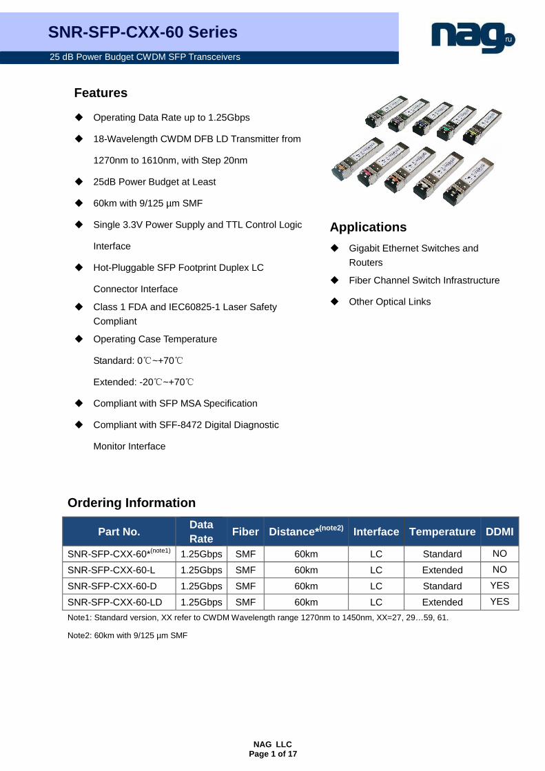
SNR-SFP-CXX-60 Series 25 dB Power Budget CWDM SFP Transceivers NAG LLC Page 1 of 17 Ordering Information Part No. Data Rate Fiber Distance* (note2) Interface Temperature DDMI SNR-SFP-CXX-60* (note1) 1.25Gbps SMF 60km LC Standard NO SNR-SFP-CXX-60-L 1.25Gbps SMF 60km LC Extended NO SNR-SFP-CXX-60-D 1.25Gbps SMF 60km LC Standard YES SNR-SFP-CXX-60-LD 1.25Gbps SMF 60km LC Extended YES Note1: Standard version, XX refer to CWDM Wavelength range 1270nm to 1450nm, XX=27, 29…59, 61. Note2: 60km with 9/125 μm SMF Features Operating Data Rate up to 1.25Gbps 18-Wavelength CWDM DFB LD Transmitter from 1270nm to 1610nm, with Step 20nm 25dB Power Budget at Least 60km with 9/125 μm SMF Single 3.3V Power Supply and TTL Control Logic Interface Hot-Pluggable SFP Footprint Duplex LC Connector Interface Class 1 FDA and IEC60825-1 Laser Safety Compliant Operating Case Temperature Standard: 0℃~+70℃ Extended: -20℃~+70℃ Compliant with SFP MSA Specification Compliant with SFF-8472 Digital Diagnostic Monitor Interface Applications Gigabit Ethernet Switches and Routers Fiber Channel Switch Infrastructure Other Optical Links
-
Upload
khangminh22 -
Category
Documents
-
view
2 -
download
0
Transcript of SNR-SFP-CXX-60 Series - ITMag.uz
SNR-SFP-CXX-60 Series 25 dB Power Budget CWDM SFP Transceivers
NAG LLC Page 1 of 17
Ordering Information
Part No. Data Rate
Fiber Distance*(note2) Interface Temperature DDMI
SNR-SFP-CXX-60*(note1) 1.25Gbps SMF 60km LC Standard NO
SNR-SFP-CXX-60-L 1.25Gbps SMF 60km LC Extended NO
SNR-SFP-CXX-60-D 1.25Gbps SMF 60km LC Standard YES
SNR-SFP-CXX-60-LD 1.25Gbps SMF 60km LC Extended YES
Note1: Standard version, XX refer to CWDM Wavelength range 1270nm to 1450nm, XX=27, 29…59, 61.
Note2: 60km with 9/125 µm SMF
Features
Operating Data Rate up to 1.25Gbps
18-Wavelength CWDM DFB LD Transmitter from
1270nm to 1610nm, with Step 20nm
25dB Power Budget at Least
60km with 9/125 µm SMF
Single 3.3V Power Supply and TTL Control Logic
Interface
Hot-Pluggable SFP Footprint Duplex LC
Connector Interface
Class 1 FDA and IEC60825-1 Laser Safety
Compliant
Operating Case Temperature
Standard: 0~+70
Extended: -20~+70
Compliant with SFP MSA Specification
Compliant with SFF-8472 Digital Diagnostic
Monitor Interface
Applications
Gigabit Ethernet Switches and
Routers
Fiber Channel Switch Infrastructure
Other Optical Links
SNR-SFP-CXX-60 Series 25 dB Power Budget CWDM SFP Transceivers
NAG LLC Page 2 of 17
CWDM* Wavelength (0~70C)
Band Nomenclature Wavelength(nm)
Min. Typ. Max.
O-band Original
A 1264 1270 1277.5
B 1284 1290 1297.5
C 1304 1310 1317.5
D 1324 1330 1337.5
E 1344 1350 1357.5
E-band Extended
F 1364 1370 1377.5
G 1384 1390 1397.5
H 1404 1410 1417.5
I 1424 1430 1437.5
J 1444 1450 1457.5
S-band Short
Wavelength
K 1464 1470 1477.5
L 1484 1490 1497.5
M 1504 1510 1517.5
N 1524 1530 1537.5
C-band Conventional O 1544 1550 1557.5
L-band
Long Wavelength
P 1564 1570 1577.5
Q 1584 1590 1597.5
R 1604 1610 1617.5
CWDM*: 18 Wavelengths from 1270nm to 1610nm, each step 20nm.
Regulatory Compliance
Feature Standard Performance Electrostatic Discharge
(ESD) to the
Electrical Pins
MIL-STD-883G
Method 3015.7 Class 1C (>1000V)
Electrostatic Discharge
to the Enclosure
EN 55024:1998+A1+A2
IEC-61000-4-2
GR-1089-CORE
Compliant with standards
Electromagnetic
Interference (EMI)
FCC Part 15 Class B
EN55022:2006
CISPR 22B :2006
VCCI Class B
Compliant with standards
Noise frequency range: 30MHz to
6GHz. Good system EMI design
practice required to achieve Class
SNR-SFP-CXX-60 Series 25 dB Power Budget CWDM SFP Transceivers
NAG LLC Page 3 of 17
B margins.
System margins are dependent
on customer host board and
chassis design.
Immunity EN 55024:1998+A1+A2
IEC 61000-4-3
Compliant with standards. 1KHz
sine-wave, 80% AM, from 80MHz
to 1GHz. No effect on
transmitter/receiver performance
is detectable between these
limits.
Laser Eye Safety
FDA 21CFR 1040.10 and 1040.11
EN (IEC) 60825-1:2007
EN (IEC) 60825-2:2004+A1
CDRH compliant and Class I laser
product.
TüV Certificate No. 50135086
Component Recognition UL and CUL
EN60950-1:2006
UL file E317337
TüV Certificate No. 50135086
(CB scheme )
RoHS6 2002/95/EC 4.1&4.2
2005/747/EC 5&7&13 Compliant with standards*note3
Note3: For update of the equipments and strict control of raw materials, SNR has the ability to supply the
customized products since Jan 1st, 2007, which meet the requirements of RoHS6 (Restrictions on use of certain
Hazardous Substances) of European Union.
In light of item 5 in RoHS exemption list of RoHS Directive 2002/95/EC, Item 5: Lead in glass of cathode ray
tubes, electronic components and fluorescent tubes.
In light of item 13 in RoHS exemption list of RoHS Directive 2005/747/EC, Item 13: Lead and cadmium in optical
and filter glass. The three exemptions are being concerned for SNR’s transceivers, because SNR’s transceivers
use glass, which may contain Pb, for components such as lenses, windows, isolators, and other electronic
components.
Product Description
The SNR-SFP-CXX-60 series single mode transceiver is small form factor pluggable module for
duplex optical data communications such as Gigabit Ethernet 1000BASE-ZX and Fiber Channel
1x SM-LC-L FC-PI. It is with the SFP 20-pin connector to allow hot plug capability.
This module is designed for single mode fiber and operates at a nominal wavelength of CWDM
wavelength. There are eight center wavelengths available from 1470nm to 1610nm, with each
step 20nm. A guaranteed minimum optical link budget of 25dB is offered.
The transmitter section uses a multiple quantum well CWDM DFB laser and is a class 1 laser
compliant according to International Safety Standard IEC-60825. The receiver section uses an
integrated InGaAs detector preamplifier (IDP) mounted in an optical header and a limiting
post-amplifier IC.
The SNR-SFP-CXX-60-D series are designed to be compliant with SFF-8472.
SNR-SFP-CXX-60 Series 25 dB Power Budget CWDM SFP Transceivers
NAG LLC Page 4 of 17
Absolute Maximum Ratings
Parameter Symbol Min. Max. Unit Storage Temperature Ts -40 +85 °C
Supply Voltage Vcc -0.5 3.6 V
Operating Relative Humidity - 95 %
*Exceeding any one of these values may destroy the device immediately.
Recommended Operating Conditions
Parameter Symbol Min. Typical Max. Unit
Operating Case
Temperature TA
SNR-SFP-CXX-60 0 +70 °C
SNR-SFP-CXX-60-L -20 +70
Power Supply Voltage Vcc 3.15 3.3 3.45 V
Power Supply Current Icc 300 mA
Date Rate GBE 1.25
Gbps FC 1.063
Performance Specifications - Electrical
Parameter Symbol Min. Typ. Max Unit Notes Transmitter
LVPECL
Inputs(Differential) Vin 400 2000 mVpp
AC coupled
inputs*(note5)
Input Impedance
(Differential) Zin 85 100 115 ohm
Rin > 100
kohm @ DC
TX_Dis Disable 2 Vcc+0.3
V
Enable 0 0.8
TX_FAULT Fault 2 Vcc+0.3
V
Normal 0 0.8
Receiver
LVPECL Outputs
(Differential) Vout 400 2000 mVpp
AC coupled
outputs*(note5
)
Output Impedance
(Differential) Zout 85 100 115 ohm
RX_LOS LOS 2 Vcc+0.3 V
Normal 0 0.8 V
MOD_DEF ( 0:2 ) VoH 2.5 V With Serial
ID VoL 0 0.5 V
SNR-SFP-CXX-60 Series 25 dB Power Budget CWDM SFP Transceivers
NAG LLC Page 5 of 17
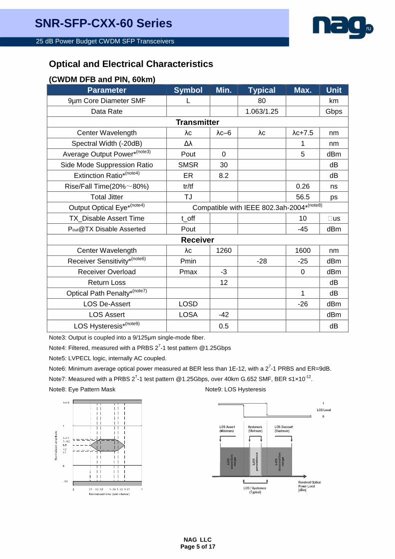
Optical and Electrical Characteristics
(CWDM DFB and PIN, 60km) Parameter Symbol Min. Typical Max. Unit
9µm Core Diameter SMF L 80 km
Data Rate 1.063/1.25 Gbps
Transmitter
Center Wavelength λc λc–6 λc λc+7.5 nm
Spectral Width (-20dB) ∆λ 1 nm
Average Output Power*(note3) Pout 0 5 dBm
Side Mode Suppression Ratio SMSR 30 dB
Extinction Ratio*(note4) ER 8.2 dB
Rise/Fall Time(20%~80%) tr/tf 0.26 ns
Total Jitter TJ 56.5 ps
Output Optical Eye*(note4) Compatible with IEEE 802.3ah-2004*(note8)
TX_Disable Assert Time t_off 10 us
Pout@TX Disable Asserted Pout -45 dBm
Receiver Center Wavelength λc 1260 1600 nm
Receiver Sensitivity*(note6) Pmin -28 -25 dBm
Receiver Overload Pmax -3 0 dBm
Return Loss 12 dB
Optical Path Penalty*(note7) 1 dB
LOS De-Assert LOSD -26 dBm
LOS Assert LOSA -42 dBm
LOS Hysteresis*(note9) 0.5 dB
Note3: Output is coupled into a 9/125µm single-mode fiber.
Note4: Filtered, measured with a PRBS 27-1 test pattern @1.25Gbps
Note5: LVPECL logic, internally AC coupled.
Note6: Minimum average optical power measured at BER less than 1E-12, with a 27-1 PRBS and ER=9dB.
Note7: Measured with a PRBS 27-1 test pattern @1.25Gbps, over 40km G.652 SMF, BER ≤1×10-12.
Note8: Eye Pattern Mask Note9: LOS Hysteresis
SNR-SFP-CXX-60 Series 25 dB Power Budget CWDM SFP Transceivers
NAG LLC Page 6 of 17
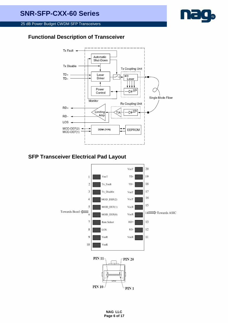
Functional Description of Transceiver
SFP Transceiver Electrical Pad Layout
SNR-SFP-CXX-60 Series 25 dB Power Budget CWDM SFP Transceivers
NAG LLC Page 7 of 17
Pin Function Definitions
Pin Num.
Name Function Plug Seq.
Notes
1 VeeT Transmitter Ground 1 5)
2 TX Fault Transmitter Fault
Indication 3 1)
3 TX Disable Transmitter Disable 3 2) Module disables on high or
open
4 MOD-DEF2 Module Definition 2 3 3) Data line for Serial ID.
5 MOD-DEF1 Module Definition 1 3 3) Clock line for Serial ID.
6 MOD-DEF0 Module Definition 0 3 3) Grounded within the
module.
7 Rate Select Not Connect 3 Function not available
8 LOS Loss of Signal 3 4)
9 VeeR Receiver Ground 1 5)
10 VeeR Receiver Ground 1 5)
11 VeeR Receiver Ground 1 5)
12 RD- Inv. Received Data Out 3 6)
13 RD+ Received Data Out 3 6)
14 VeeR Receiver Ground 1 5)
15 VccR Receiver Power 2 7) 3.3 ± 5%
16 VccT Transmitter Power 2 7) 3.3 ± 5%
17 VeeT Transmitter Ground 1 5)
18 TD+ Transmit Data In 3 8)
19 TD- Inv. Transmit Data In 3 8)
20 VeeT Transmitter Ground 1 5)
1) TX Fault is an open collector/drain output, which should be pulled up with a 4.7K – 10KΩ
resistor on the host board. Pull up voltage between 2.0V and VccT, R+0.3V. When high, output
indicates a laser fault of some kind. Low indicates normal operation. In the low state, the output
will be pulled to < 0.8V.
2) TX disable is an input that is used to shut down the transmitter optical output. It is pulled up
within the module with a 4.7 – 10 KΩ resistor. Its states are:
Low (0 – 0.8V): Transmitter on
(>0.8, < 2.0V): Undefined
High (2.0 – 3.465V): Transmitter Disabled
Open: Transmitter Disabled
3) Modulation Absent, connected to VEET or VEER in the module.
4) LOS (Loss of Signal) is an open collector/drain output, which should be pulled up with a 4.7K –
10KΩ resistor. Pull up voltage between 2.0V and VccT, R+0.3V. When high, this output indicates
Notes:
SNR-SFP-CXX-60 Series 25 dB Power Budget CWDM SFP Transceivers
NAG LLC Page 8 of 17
the received optical power is below the worst-case receiver sensitivity (as defined by the
standard in use). Low indicates normal operation. In the low state, the output will be pulled to <
0.8V.
5) VeeR and VeeT may be internally connected within the SFP module.
6) RD-/+: These are the differential receiver outputs. They are AC coupled 100Ω differential lines
which should be terminated with 100Ω (differential) at the user SERDES. The AC coupling is
done inside the module and is thus not required on the host board. The voltage swing on these
lines will be between 400 and 2000mV differential (200 –1000mV single ended) when properly
terminated.
7) VccR and VccT are the receiver and transmitter power supplies. They are defined as 3.3V
±5% at the SFP connector pin. Maximum supply current is 300mA. Recommended host board
power supply filtering is shown below. Inductors with DC resistance of less than 1 ohm should be
used in order to maintain the required voltage at the SFP input pin with 3.3V supply voltage.
When the recommended supply-filtering network is used, hot plugging of the SFP transceiver
module will result in an inrush current of no more than 30mA greater than the steady state value.
VccR and VccT may be internally connected within the SFP transceiver module.
8) TD-/+: These are the differential transmitter inputs. They are AC-coupled, differential lines with
100Ω differential termination inside the module. The AC coupling is done inside the module and
is thus not required on the host board. The inputs will accept differential swings of 400 – 2000mV
(200 – 1000mV single-ended).
The serial interface uses the 2-wire serial CMOS EEPROM protocol defined for the ATMEL
AT24C02/04 family of components. When the serial protocol is activated, the host generates the
serial clock signal (SCL). The positive edge clocks data into those segments of the EEPROM that
are not write protected within the SFP transceiver. The negative edge clocks data from the SFP
transceiver. The serial data signal (SDA) is bi-directional for serial data transfer. The host uses
SDA in conjunction with SCL to mark the start and end of serial protocol activation. The
memories are organized as a series of 8-bit data words that can be addressed individually or
sequentially.
The Module provides diagnostic information about the present operating conditions. The
transceiver generates this diagnostic data by digitization of internal analog signals. Calibration
and alarm/warning threshold data is written during device manufacture. Received power
monitoring, transmitted power monitoring, bias current monitoring, supply voltage monitoring and
temperature monitoring all are implemented. If the module is defined as external calibrated, the
diagnostic data are raw A/D values and must be converted to real world units using calibration
constants stored in EEPROM locations 56 – 95 at wire serial bus address A2H. The digital
diagnostic memory map specific data field define as following .For detail EEPROM information,
please refer to the related document of SFF 8472 Rev 9.3.
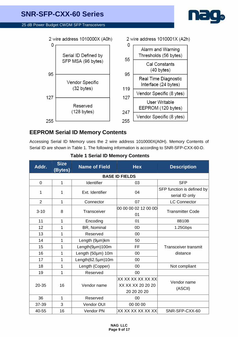
EEPROM
SNR-SFP-CXX-60 Series 25 dB Power Budget CWDM SFP Transceivers
NAG LLC Page 9 of 17
EEPROM Serial ID Memory Contents
Accessing Serial ID Memory uses the 2 wire address 1010000X(A0H). Memory Contents of
Serial ID are shown in Table 1. The following information is according to SNR-SFP-CXX-60-D.
Table 1 Serial ID Memory Contents
Addr. Size
(Bytes) Name of Field Hex Description
BASE ID FIELDS 0 1 Identifier 03 SFP
1 1 Ext. Identifier 04 SFP function is defined by
serial ID only
2 1 Connector 07 LC Connector
3-10 8 Transceiver 00 00 00 02 12 00 0D
01 Transmitter Code
11 1 Encoding 01 8B10B
12 1 BR, Nominal 0D 1.25Gbps
13 1 Reserved 00
14 1 Length (9µm)km 50
Transceiver transmit
distance
15 1 Length(9µm)100m FF
16 1 Length (50µm) 10m 00
17 1 Length(62.5µm)10m 00
18 1 Length (Copper) 00 Not compliant
19 1 Reserved 00
20-35 16 Vendor name
XX XX XX XX XX XX
XX XX XX 20 20 20
20 20 20 20
Vendor name
(ASCII)
36 1 Reserved 00
37-39 3 Vendor OUI 00 00 00
40-55 16 Vendor PN XX XX XX XX XX XX SNR-SFP-CXX-60
SNR-SFP-CXX-60 Series 25 dB Power Budget CWDM SFP Transceivers
NAG LLC Page 10 of 17
XX XX XX XX XX XX
XX XX XX 20 20 20
56-59 4 Vendor rev 31 2E 30 20 1.0
60-61 2 Wavelength XX XX CWDM, XXXXnm
62 1 Reserved 00
63 1 CC_BASE Check Sum
(Variable)
Check code for Base ID
Fields
EXTENDED ID FIELDS
64-65 2 Options 00 1A
TX_DISABLE, TX_FAULT
and Loss of Signal
implemented.
66 1 BR, max 00
67 1 BR, min 00
68-83 16 Vendor SN
XX XX XX XXXX XX
XX XX 20 20 20 20
20 20 20 20(note9)
Serial Number of
transceiver (ASCII). For
example “B000822”.
84-91 8 Date code XX XX XX XX XX XX
XX XX(note9)
Manufactory date code.
For example “080405”.
92 1 Diagnostic
Monitoring Type XX(note9)
Digital diagnostic
monitoring implemented
93 1 Enhanced Options XX(note9) Optional flags
94 1 SFF_8472
Compliance XX(note9) 01 for Rev9.3 SFF-8472.
95 1 CC_EXT Check Sum
(Variable)
Check sum for Extended ID
Field.
VENDOR SPECIFIC ID FIELDS
96-127 32 Vendor Specific Read only Depends on customer
information
128-255 128 Reserved Read only
Note9: The “xx” byte should be filled in according to practical case. For more information, please refer to the
related document of SFP Multi-Source Agreement (MSA).
Digital Diagnostic Monitoring Interface (2-Wire Address A2H)
Alarm and Warning Thresholds (2 Wire Address A2H) Address # Bytes Name of Field Real Value Unit
00-01 2 Temp High Alarm 110 Degree C
02-03 2 Temp Low Alarm -45 Degree C
04-05 2 Temp High Warning 95 Degree C
06-07 2 Temp Low Warning -42 Degree C
08-09 2 Voltage High Alarm 3.6 V
10-11 2 Voltage Low Alarm 2.9 V
12-13 2 Voltage High Warning 3.5 V
14-15 2 Voltage Low Warning 3.0 V
SNR-SFP-CXX-60 Series 25 dB Power Budget CWDM SFP Transceivers
NAG LLC Page 11 of 17
16-17 2 Bias High Alarm 90 mA
18-19 2 Bias Low Alarm 2 mA
20-21 2 Bias High Warning 80 mA
22-23 2 Bias Low Warning 3 mA
24-25 2 TX Power High Alarm 6 dBm
26-27 2 TX Power Low Alarm -1 dBm
28-29 2 TX Power High Warning 5 dBm
30-31 2 TX Power Low Warning 0 dBm
32-33 2 RX Power High Alarm -3 dBm
34-35 2 RX Power Low Alarm -25 dBm
36-37 2 RX Power High Warning -4 dBm
38-39 2 RX Power Low Warning -24 dBm
40-55 16 Reserved
Calibration Constants (2 Wire Address A2H) Address # Bytes Name of Field HEX Description
56-59 4 RX_PWR (4) 00 00 00
00
Set to zero for “internally calibrated”
devices.
60-63 4 RX_PWR (3) 00 00 00
00
Set to zero for “internally calibrated”
devices.
64-67 4 RX_PWR (2) 00 00 00
00
Set to zero for “internally calibrated”
devices.
68-71 4 RX_PWR (1) 3F 80 00
00 Set to 1 for “internally calibrated” devices.
72-75 4 RX_PWR (0) 00 00 00
00
Set to zero for “internally calibrated”
devices.
76-77 2 TX_I (Slope) 01 00 Set to 1 for “internally calibrated” devices.
78-79 2 TX_I (Offset) 00 00 Set to zero for “internally calibrated”
devices.
80-81 2 TX_PWR
(Slope) 01 00 Set to 1 for “internally calibrated” devices.
82-83 2 TX_PWR
(Offset) 00 00
Set to zero for “internally calibrated”
devices.
84-85 2 T (Slope) 01 00 Set to 1 for “internally calibrated” devices.
86-87 2 T (Offset) 00 00 Set to zero for “internally calibrated”
devices.
88-89 2 V (Slope) 01 00 Set to 1 for “internally calibrated” devices.
90-91 2 V (Offset) 00 00 Set to zero for “internally calibrated”
devices.
92-94 3 Reserved 00 00 00 Reserved
95 1 Checksum XX Checksum of bytes 0 – 94.
A/D Value (2 Wire Address A2H) Address # Bytes Name of Field Description
96-97 2 Temperature (MSB, LSB) Internally measured module temperature
SNR-SFP-CXX-60 Series 25 dB Power Budget CWDM SFP Transceivers
NAG LLC Page 12 of 17
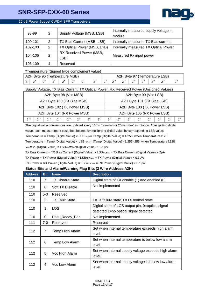
98-99 2 Supply Voltage (MSB, LSB) Internally measured supply voltage in
module
100-101 2 TX Bias Current (MSB, LSB) Internally measured TX Bias current
102-103 2 TX Optical Power (MSB, LSB) Internally measured TX Optical Power
104-105 2 RX Received Power (MSB,
LSB) Measured Rx input power
106-109 4 Reserved
*Temperature (Signed twos complement value) A2H Byte 96 (Temperature MSB) A2H Byte 97 (Temperature LSB) S 26 25 24 23 22 21 20 2-1 2-2 2-3 2-4 2-5 2-6 2-7 2-8
Supply Voltage, TX Bias Current, TX Optical Power, RX Received Power (Unsigned Values)
A2H Byte 98 (Vcc MSB) A2H Byte 99 (Vcc LSB)
A2H Byte 100 (TX Bias MSB) A2H Byte 101 (TX Bias LSB)
A2H Byte 102 (TX Power MSB) A2H Byte 103 (TX Power LSB)
A2H Byte 104 (RX Power MSB) A2H Byte 105 (RX Power LSB)
215 214 213 212 211 210 29 28 27 26 25 24 23 22 21 20
The digital value conversions are updated every 13ms (nominal) or 20ms (max) in rotation. After getting digital
value, each measurement could be obtained by multiplying digital value by corresponding LSB value:
Temperature = Temp (Digital Value) × LSBTemp = Temp (Digital Value) × 1/256; when Temperature<128
Temperature = Temp (Digital Value) × LSBTemp = [Temp (Digital Value) ×1/256]-256; when Temperature≧128
Vcc = Vcc(Digital Value) × LSBVcc=VCC(Digital Value) × 100µV
TX Bias Current = TX Bias Current (Digital Value) × LSBTX,Bias = TX Bias Current (Digital Value) × 2µA
TX Power = TX Power (Digital Value) × LSBTXPower = TX Power (Digital Value) × 0.1µW
RX Power = RX Power (Digital Value) × LSBRXPower = RX Power (Digital Value) × 0.1µW
Status Bits and Alarm/Warning Flag Bits (2 Wire Address A2H)
Address Bit Name Description
110 7 TX Disable State Digital state of TX disable (1) and enabled (0)
110 6 Soft TX Disable Not implemented
110 5-3 Reserved
110 2 TX Fault State 1=TX failure state, 0=TX normal state
110 1 LOS Digital state of LOS output pin. 0=optical signal
detected,1=no optical signal detected
110 0 Data_Ready_Bar Not implemented.
111 7-0 Reserved Reserved
112 7 Temp High Alarm Set when internal temperature exceeds high alarm
level.
112 6 Temp Low Alarm Set when internal temperature is below low alarm
level.
112 5 Vcc High Alarm Set when internal supply voltage exceeds high alarm
level.
112 4 Vcc Low Alarm Set when internal supply voltage is below low alarm
level.
SNR-SFP-CXX-60 Series 25 dB Power Budget CWDM SFP Transceivers
NAG LLC Page 13 of 17
112 3 TX Bias High Alarm Set when TX Bias current exceeds high alarm level.
112 2 TX Bias Low Alarm Set when TX Bias current is below low alarm level.
112 1 TX Power High Alarm Set when TX Power exceeds high alarm level.
112 0 TX Power Low Alarm Set when TX Power is below low alarm level.
113 7 RX Power High Alarm Set when Received Power exceeds high alarm level.
113 6 RX Power Low Alarm Set when Received Power is below low alarm level.
113 5-0 Reserved Alarm
114-115 All Reserved
116 7 Temp High Warning Set when internal temperature exceeds high warning
level.
116 6 Temp Low Warning Set when internal temperature is below low warning
level.
116 5 Vcc High Warning Set when internal supply voltage >high warning level.
116 4 Vcc Low Warning Set when internal supply voltage < low warning level.
116 3 TX Bias High Warning Set when TX Bias current exceeds high warning level.
116 2 TX Bias Low Warning Set when TX Bias current is below low warning level.
116 1 TX Power High
Warning Set when TX Power exceeds high warning level.
116 0 TX Power Low
Warning Set when TX Power is below low warning level.
117 7 RX Power High
Warning
Set when Received Power exceeds high warning
level.
117 6 RX Power Low
Warning Set when Received Power is below low warning level.
117 5-0 Reserved Warning
118-119 All Reserved
Vendor Specific and User Accessible EEPROM (2 Wire Address A2H)
Address # Bytes Name Description
120-127 8 Vendor Specific Don’t Access
128-247 120 User writable EEPROM
248-255 8 Vendor Specific Don’t Access
SNR-SFP-CXX-60 Series 25 dB Power Budget CWDM SFP Transceivers
NAG LLC Page 14 of 17
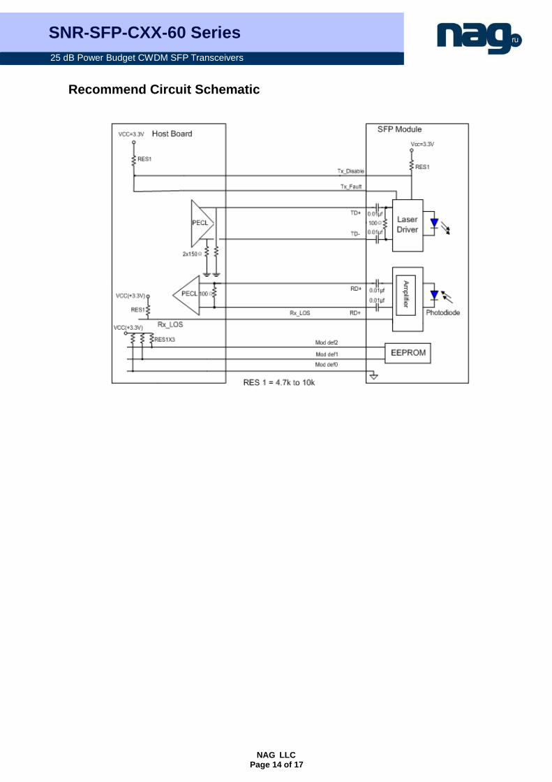
Recommend Circuit Schematic

SNR-SFP-CXX-60 Series 25 dB Power Budget CWDM SFP Transceivers
NAG LLC Page 15 of 17
Mechanical Specifications
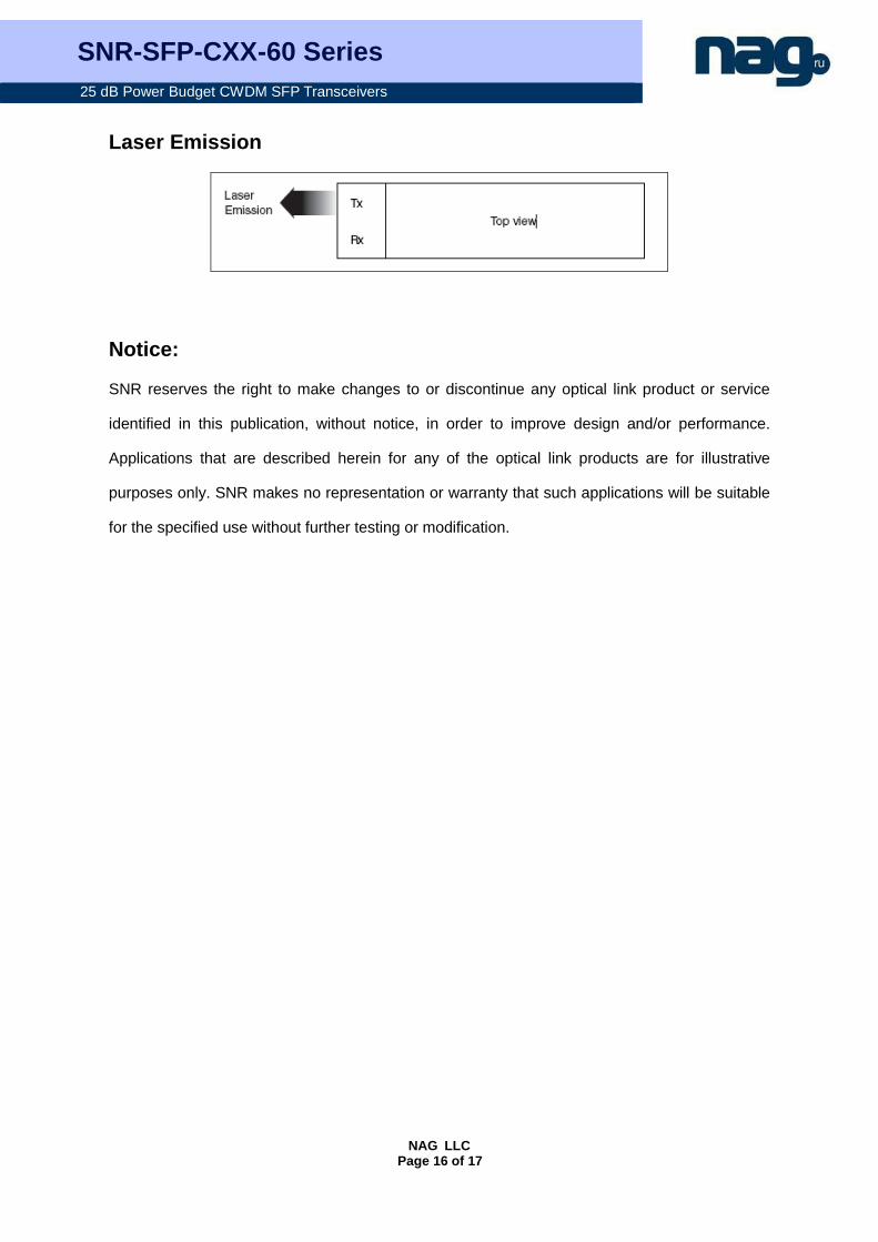
Class 1 Labels
Laser Emission Data
Wavelength >1460nm
Total output power (as defined by FDA: 7mm aperture at 20cm distance) <0.79mW
Total output power (as defined by IEC: 7mm aperture at 10cm distance) <10mW
Beam divergence 12.5°
SNR-SFP-CXX-60 Series 25 dB Power Budget CWDM SFP Transceivers
NAG LLC Page 16 of 17
Laser Emission
Notice:
SNR reserves the right to make changes to or discontinue any optical link product or service
identified in this publication, without notice, in order to improve design and/or performance.
Applications that are described herein for any of the optical link products are for illustrative
purposes only. SNR makes no representation or warranty that such applications will be suitable
for the specified use without further testing or modification.
SNR-SFP-CXX-60 Series 25 dB Power Budget CWDM SFP Transceivers
NAG LLC Page 17 of 17
GUARANTEE:
CONTACT: Addres: Building 118, Vonsovskogo Street 1, Yekaterinburg, Russia Tel: +7(343) 379-98-38 Fax: +7(343) 379-98-38 E-mail: [email protected] Online shop: http://shop.nag.ru