SmartRF® Studio User Manual Rev. 6.10.0
119
SmartRF® Studio User Manual Rev. 6.10.0 SmartRF ® 03 SmartRF ® 04 1/118
-
Upload
khangminh22 -
Category
Documents
-
view
0 -
download
0
Transcript of SmartRF® Studio User Manual Rev. 6.10.0
SmartRF® Studio User Manual Rev. 6.10.0
SmartRF® 03
SmartRF® 04 1/118
Table of contents
1. INTRODUCTION 4 2. INSTALLATION 4 3. OVERVIEW OF SMARTRF® 01/02 STUDIO 5
3.1 STARTING SMARTRF® STUDIO FOR CCX00/CC10XX 5 3.2 PULL-DOWN MENUS 5
3.2.1 File 6 3.2.2 View 7 3.2.3 Configuration 7 3.2.4 Tools 8 3.2.5 Help 8
3.3 THE SMARTRF® STUDIO TOOLBAR 9 3.4 THE STATUS INFORMATION 9
4. SMARTRF® STUDIO FOR CC400/CC900 10 4.1 THE NORMAL CONFIGURATION WINDOW FOR CC400/CC900 11
4.1.1 System parameters 12 4.2 THE REGISTER CONFIGURATION WINDOW FOR CC400/CC900 17 4.3 DESCRIPTION OF THE TOOLS FOR CC400/CC900 18
4.3.1 Programming 18 4.3.2 EEPROM-programming 19 4.3.3 FLASH-programming 20
5. SMARTRF® STUDIO FOR CC1000 21 5.1 THE NORMAL CONFIGURATION WINDOW FOR CC1000 22
5.1.1 System parameters 23 5.2 THE REGISTER CONFIGURATION WINDOW FOR CC1000 28 5.3 EVALUATION BOARD CONTROL 29
6. SMARTRF® STUDIO FOR CC1050 30 6.1 THE NORMAL CONFIGURATION WINDOW FOR CC1050 31
6.1.1 System parameters 32 6.2 THE REGISTER CONFIGURATION WINDOW FOR CC1050 35 6.3 EVALUATION BOARD CONTROL 36
7. SMARTRF® STUDIO FOR CC1010 37 7.1 THE NORMAL CONFIGURATION WINDOW FOR CC1010 38
7.1.1 System parameters 39 7.2 THE REGISTER CONFIGURATION WINDOW FOR CC1010 43 7.3 EVALUATION BOARD CONTROL 44
8. SMARTRF® STUDIO FOR CC102X 45 8.1 THE NORMAL CONFIGURATION WINDOW FOR CC102X 46
8.1.1 System parameters 47 8.2 THE REGISTER CONFIGURATION WINDOW FOR CC102X 52 8.3 EVALUATION BOARD CONTROL 53
9. SMARTRF® STUDIO FOR CC1070 54 9.1 THE NORMAL CONFIGURATION WINDOW FOR CC1070 55
9.1.1 System parameters 56 9.2 THE REGISTER CONFIGURATION WINDOW FOR CC1070 60 9.3 EVALUATION BOARD CONTROL 61
10. SMARTRF® STUDIO FOR CC2400 62 10.1 STARTING SMARTRF® STUDIO AND SELECTING A CC2400 DEVICE 62 10.2 OVERVIEW OF SMARTRF® STUDIO FOR CC2400 63
2/118
10.2.1 Register Status 63 10.2.2 System Configuration 65 10.2.3 Pull-down menus and toolbar 68 10.2.4 Online help 71
11. SMARTRF® STUDIO FOR CC2420/2430/2431 72 11.1 STARTING SMARTRF® STUDIO AND SELECTING A CC2420/2430/2431 DEVICE 72 11.2 OVERVIEW OF SMARTRF® STUDIO FOR CC2420/2430/2431 74
11.2.1 Register Status 74 11.2.2 System Configuration 76 11.2.3 Online help 86
12. SMARTRF® STUDIO FOR CC11XX AND 25XX 87 12.1 STARTING SMARTRF® STUDIO AND SELECTING A CC111X/251X DEVICE 87 12.2 OVERVIEW OF SMARTRF® STUDIO FOR CC11XX/25XX 89
12.2.1 Register Status 89 12.2.2 System Configuration 91 12.2.3 Pull-down menus and toolbar 100 12.2.4 Online help 103
13. SMARTRF® STUDIO FOR CC2520 104 13.1 STARTING SMARTRF® STUDIO AND SELECT A CC2520 DEVICE 104 13.2 OVERVIEW OF SMARTRF® STUDIO FOR CC2520 105
13.2.1 Register Status 106 13.2.2 View Panels 107 13.2.3 Pull-down menus and toolbar 113 13.2.4 Online help 116
14. SMARTRF® STUDIO GENERAL NOTES. 116 14.1 STARTUP PROBLEM. 116
15. ADDRESS INFORMATION 118
3/118
1. Introduction This user manual describes how to use SmartRF® Studio. This software is developed by Texas Instruments to the courtesy of our customers. This software is made to configure the RFICs on the Evaluation Board for the CC400, CC900, CC1000 , CC1050, CC1010, CC1020, CC1021, CC1070, CC2400, CC2420, CC2430, CC2431, CC1100, CC1101, CC1110, CC1111, CC1150,. CC2500, CC2510, CC2511, CC2520 and CC2550. By giving out this software the designers of radio systems can easily evaluate the RFICs at an early stage in the design-process. It is further a useful tool during the generation of the configuration data and for finding optimized external component values. It is also a helpful tool to get to know the RFICs from Texas Instruments. Distribution and disclaimer: This software may be distributed freely under the condition that no profit is gained from its distribution, nor from any other program distributed in the same package. All files that are part of this package have to be distributed together and none of them may be changed in any way other than archiving or crunching. This program is distributed as freeware (and giftware). This package is provided “as is” without warranty of any kind. The author assumes no responsibility or liability whatsoever for any damage or loss of data caused by using this package. General information: Texas Instruments believes the furnished information is correct and accurate at the time of this printing. However, Texas Instruments reserves the right to make changes to this product without notice. Texas Instruments does not assume any responsibility for the use of the described product. Please refer to Texas Instruments web site for the latest update. SmartRF® is a registered trademark of Texas Instruments. SmartRF is Texas Instruments RF technology platform with RF library cells, modules and design expertise. Based on SmartRF Texas Instruments develops standard component RF-circuits as well as full custom ASICs based on customers' requirements.
2. Installation A SmartRF® Studio set-up file is available from the Texas Instruments web-site at www.ti.com. Make sure that you have the newest version available before you start the installation. To begin the installation: Run the set-up file and follow the instructions. SmartRF® Studio communicates with the evaluation boards through the USB port (SmartRF®03/04/05) or the parallel port (SmartRF®01/02). Up to eight USB devices are supported on a single computer. The platform you can use SmartRF® Studio will for this reason depend in the device you want to evaluate. USB port devices (SmartRF®03/04/05) are supported on the following platforms: Windows 98 Windows 2000 Windows XP Parallel port devices (CCX00/CC10X0) are supported on the following platforms: Windows 98 Windows 2000 Windows NT Windows XP Other system parameters are not critical. 4/118

3. Overview of SmartRF® 01/02 Studio
3.1 Starting SmartRF® Studio for CCX00/CC10XX Before you can start to use SmartRF® Studio for the SmartRF® 01 or 02 productline (CCX00/CC10XX), you must select a device to evaluate. This is done by activating the SmartRF® 01 or SmartRF® 02 tag in the device manager of SmartRF® Studio. Double-click on the device to open the SmartRF® Studio for this device. You can also mark the device and click on the start button.
The file version button will list up the version of all files included in this version of SmartRF® Studio.
3.2 Pull-down menus SmartRF® Studio simplifies access to its features through the use of pull-down menus. The SmartRF® Studio menus are shown below.
5/118
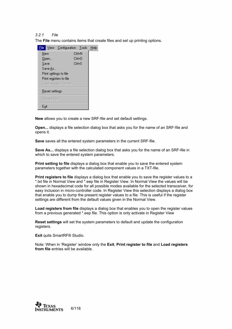
3.2.1 File The File menu contains items that create files and set up printing options.
New allows you to create a new SRF-file and set default settings. Open... displays a file selection dialog box that asks you for the name of an SRF-file and opens it. Save saves all the entered system parameters in the current SRF-file. Save As... displays a file selection dialog box that asks you for the name of an SRF-file in which to save the entered system parameters. Print setting to file displays a dialog box that enable you to save the entered system parameters together with the calculated component values in a TXT-file. Print registers to file displays a dialog box that enable you to save the register values to a *.txt file in Normal View and *.eep file in Register View. In Normal View the values will be shown in hexadecimal code for all possible modes available for the selected transceiver, for easy inclusion in micro-controller code. In Register View this selection displays a dialog box that enable you to dump the present register values to a file. This is useful if the register settings are different from the default values given in the Normal View. Load registers from file displays a dialog box that enables you to open the register values from a previous generated *.eep file. This option is only activate in Register View Reset settings will set the system parameters to default and update the configuration registers. Exit quits SmartRF® Studio. Note: When in ‘Register’ window only the Exit, Print register to file and Load registers from file entries will be available.
6/118
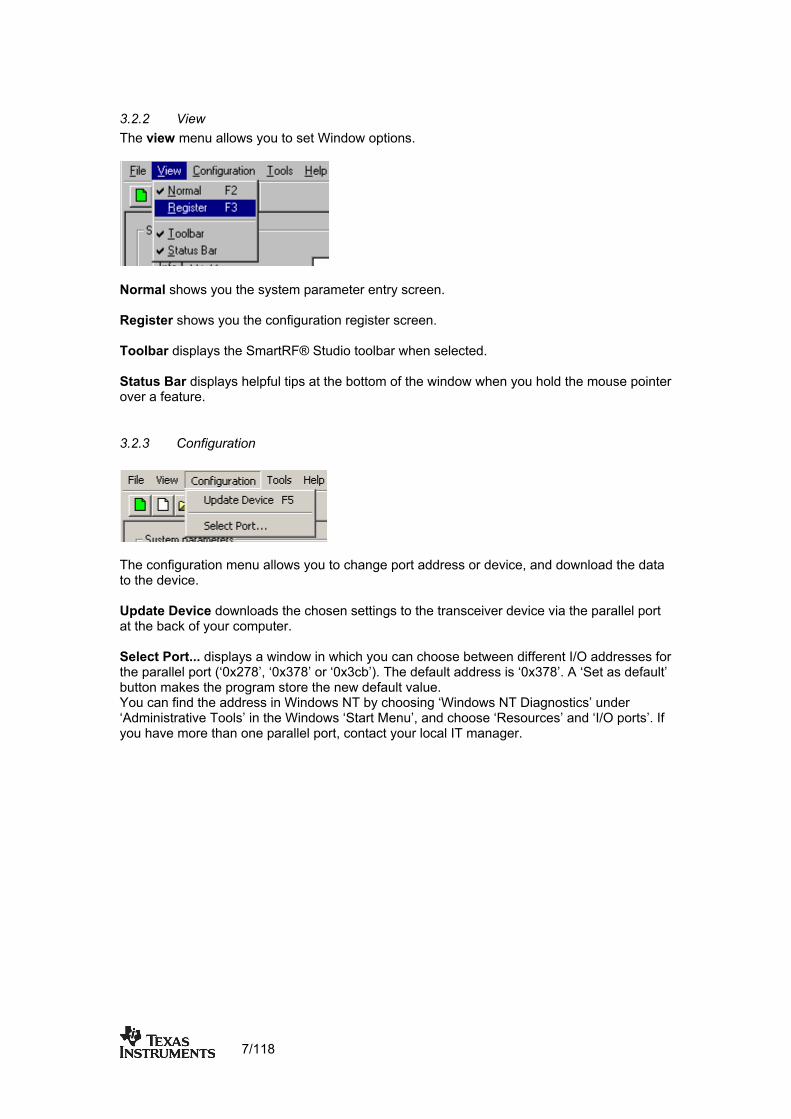
3.2.2 View The view menu allows you to set Window options.
Normal shows you the system parameter entry screen. Register shows you the configuration register screen. Toolbar displays the SmartRF® Studio toolbar when selected. Status Bar displays helpful tips at the bottom of the window when you hold the mouse pointer over a feature.
3.2.3 Configuration
The configuration menu allows you to change port address or device, and download the data to the device. Update Device downloads the chosen settings to the transceiver device via the parallel port at the back of your computer. Select Port... displays a window in which you can choose between different I/O addresses for the parallel port (‘0x278’, ‘0x378’ or ‘0x3cb’). The default address is ‘0x378’. A ‘Set as default’ button makes the program store the new default value. You can find the address in Windows NT by choosing ‘Windows NT Diagnostics’ under ‘Administrative Tools’ in the Windows ‘Start Menu’, and choose ‘Resources’ and ‘I/O ports’. If you have more than one parallel port, contact your local IT manager.
7/118

3.2.4 Tools
The Tool menus have an option to select programming. This is a small program that let you program the CC400 and CC900 Demonstration Board. For more information on how this program works see chapter 4.3.
3.2.5 Help
The help menu provides access to useful information about the product. Help Topics brings up a message box stating where you can find further help. About SmartRF® Studio brings up a message box with the software revision and copyright information. Contact Texas Instruments brings up a message box where you can find Texas Instruments contact information and links to our web-site and mail.
8/118

3.3 The SmartRF® Studio toolbar In addition to the pull-down menus, the toolbar provides you with simplified access to useful SmartRF® Studio and Windows features: Icon Name Description
Reset settings:Sets the system parameters to default and updates the configuration registers. New: Allows you to create a new SRF-file. Open: Displays a file selection dialog box that asks you for the name of an SRF-file and opens it. Save: Saves all the entered system parameters in the current SRF-file.
Help topics: Brings up a message box stating where you can find further help.
3.4 The status information You will find status information at the bottom of the program window. This is shown in the figure below.
The user can observe the current consumption of the transceiver in the different settings in the Normal View. SmartRF® Studio also monitors the lock pin of the transceiver. The Update device button downloads the chosen settings to the transceiver device via the parallel port (F5 can be used as a shortcut).
The bitmap of Texas Instruments is a link to the Texas Instruments homepage. By clicking on this picture, your default browser goes to our website, where you can find more information about our RF transceivers and us. At the bottom of the window, there is a status bar, which provides hints about the various features in the program.
9/118
4. SmartRF® Studio for CC400/CC900 When CC400/CC900 is used, the program has two configuration views. The parameter entry screen is the default window and can be chosen by pressing F2 or selecting Normal from the View menu. In this window you can change the system parameters, get status information and component values. The other configuration window is the “register” configuration, which is selected by pressing F3 or selecting Register from the View menu. It gives you the possibility to change the bits in the configuration registers directly. This window is mainly used to give additional information and we dissuade you to change the bits. To send the configuration data to the transceiver chip, press F5 or select Update Device from the Configuration menu or press the Update device button at the bottom of the screen. Note: When pressing Enter the parameters will be checked and component values will be calculated, but the transceiver will not be programmed until Update device is activated.
10/118
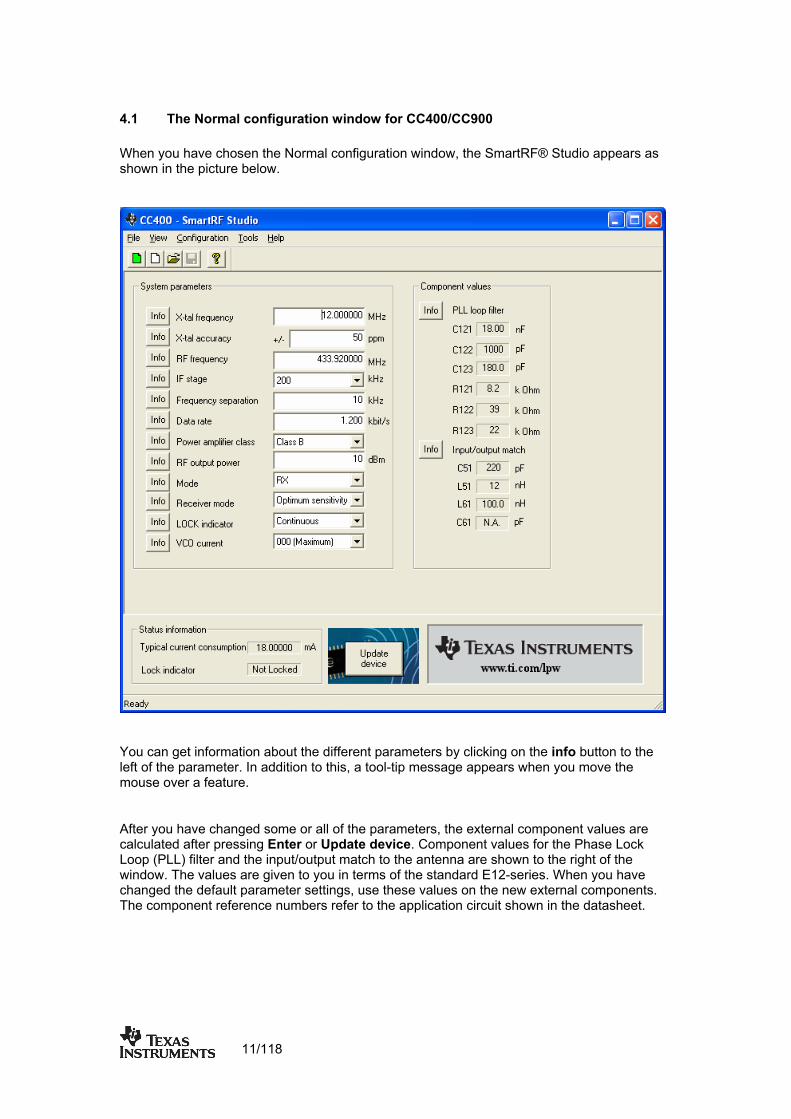
4.1 The Normal configuration window for CC400/CC900 When you have chosen the Normal configuration window, the SmartRF® Studio appears as shown in the picture below.
You can get information about the different parameters by clicking on the info button to the left of the parameter. In addition to this, a tool-tip message appears when you move the mouse over a feature.
After you have changed some or all of the parameters, the external component values are calculated after pressing Enter or Update device. Component values for the Phase Lock Loop (PLL) filter and the input/output match to the antenna are shown to the right of the window. The values are given to you in terms of the standard E12-series. When you have changed the default parameter settings, use these values on the new external components. The component reference numbers refer to the application circuit shown in the datasheet.
11/118
Using the specified component values for the PLL loop filter will give an optimum loop bandwidth for the selected system parameters. If you need a faster PLL settling time, i.e. a larger loop bandwidth, the data rate can be set to a higher value and the corresponding component values can be used. Using the specified component values for the input/output match will give an optimum match at the specified operating frequency. Minor tuning of the component values may be necessary to compensate for layout parasitics.
4.1.1 System parameters This chapter describes the different parameters and the options you have when changing them. The default parameter list is given at the end of the chapter. For detailed information on parameter setting of CC400 and CC900 see Application note AN005.
X-tal frequency
The crystal frequency of your Development Kit evaluation board is 12.000000 MHz. Do not change the X-tal frequency parameter when using this module unless the crystal is being replaced. If you are using this program to generate configuration data for your special application, use a crystal frequency between 4.000 and 13.100 MHz and replace the crystal on the printed circuit board. The crystal should be designed for 12pF load capacitance. The frequency value is rounded to 6 digits after the MHz decimal point, i.e. 12.000000 MHz.
X-tal accuracy
Enter the total crystal accuracy between 0 and 500 ppm, including initial tolerance, temperature stability, loading and ageing. If you are using a trimming capacitor to adjust the crystal oscillator, the initial tolerance will be zero. The crystal accuracy is very important for narrow-band applications (i.e. 25 kHz-channel separation). For applications using wider bands crystal accuracy is not that important. The crystal stability has an influence on the minimum possible IF filter bandwidth and the maximum frequency separation that can be used. For highest possible sensitivity it is an advantage to use a crystal with high frequency accuracy (<20 ppm). For low cost applications, however, this can be a trade-off. The default value is 30 ppm.
RF frequency
The CC900 can operate at frequencies between 800 and 1000 MHz. The Development Kit evaluation board is optimised for operation in the ISM band at 868-870 MHz. However, it is possible to use the evaluation board for frequencies between approximately 850 and 910 MHz restricted by the VCO tank tuning range. The CC400 can operate at frequencies between 300 and 500 MHz in 250 Hz steps. The Development Kit evaluation board is optimised for operation in the ISM band at 433.920 MHz. However, it is possible to use the evaluation board for frequencies between approximately 400 and 460 MHz restricted by the VCO tank tuning range. Choosing frequencies outside this range will not work for this evaluation board and should only be done for generation of configuration data to be used in other applications. Note: Depending on the crystal frequency, some RF frequencies are not allowed and an error message will pop up.
12/118
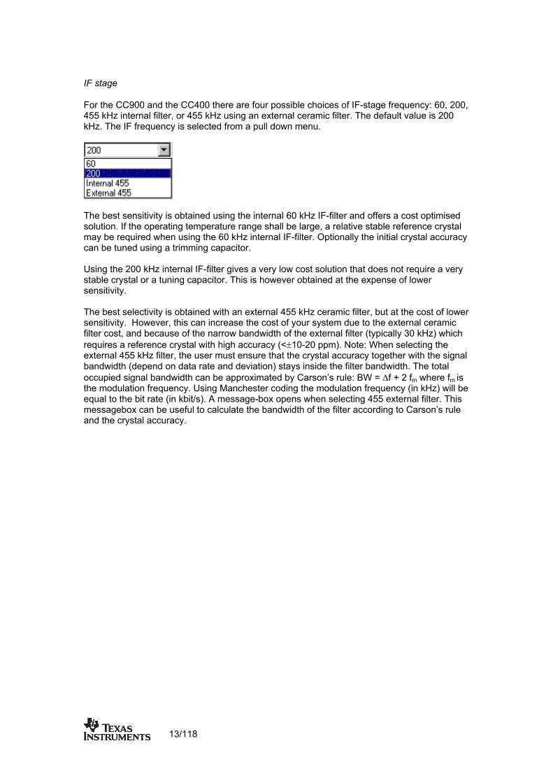
IF stage
For the CC900 and the CC400 there are four possible choices of IF-stage frequency: 60, 200, 455 kHz internal filter, or 455 kHz using an external ceramic filter. The default value is 200 kHz. The IF frequency is selected from a pull down menu.
The best sensitivity is obtained using the internal 60 kHz IF-filter and offers a cost optimised solution. If the operating temperature range shall be large, a relative stable reference crystal may be required when using the 60 kHz internal IF-filter. Optionally the initial crystal accuracy can be tuned using a trimming capacitor. Using the 200 kHz internal IF-filter gives a very low cost solution that does not require a very stable crystal or a tuning capacitor. This is however obtained at the expense of lower sensitivity. The best selectivity is obtained with an external 455 kHz ceramic filter, but at the cost of lower sensitivity. However, this can increase the cost of your system due to the external ceramic filter cost, and because of the narrow bandwidth of the external filter (typically 30 kHz) which requires a reference crystal with high accuracy (<±10-20 ppm). Note: When selecting the external 455 kHz filter, the user must ensure that the crystal accuracy together with the signal bandwidth (depend on data rate and deviation) stays inside the filter bandwidth. The total occupied signal bandwidth can be approximated by Carson’s rule: BW = ∆f + 2 fm where fm is the modulation frequency. Using Manchester coding the modulation frequency (in kHz) will be equal to the bit rate (in kbit/s). A message-box opens when selecting 455 external filter. This messagebox can be useful to calculate the bandwidth of the filter according to Carson’s rule and the crystal accuracy.
13/118
Frequency separation
The frequency separation, ∆f, is the difference between the frequency transmitted for a ‘0’ (f0) and a ‘1’ (f1). That is, f0 = fC - ∆f/2 and f1 = fC + ∆f/2 where fC is the carrier frequency entered in the ‘RF frequency’ field. The frequency separation can be adjusted between 1 and 200 kHz in 1 kHz steps. The default value is 20 kHz. Depending on the chosen IF stage the recommended frequency separation is 5 - 40 kHz for IF = 60 kHz, 10 - 100 kHz for IF = 200 kHz. 5 – 20 kHz for IF = 455 kHz with external filter The sensitivity depends slightly on frequency separation.
Data rate
The data rate can be set between 0.3 and 9.6 kbitps. The default setting is 1.2 kbitps. The data signal transmitted to the DIO pin must be Manchester encoded. The noise bandwidth of the receiver will be optimised to the selected data rate. Note that the baud rate is twice the bit rate when using Manchester coding.
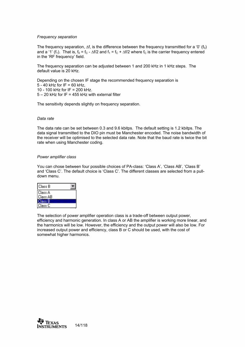
Power amplifier class
You can chose between four possible choices of PA-class: ‘Class A’, ‘Class AB’, ‘Class B’ and ‘Class C’. The default choice is ‘Class C’. The different classes are selected from a pull-down menu.
The selection of power amplifier operation class is a trade-off between output power, efficiency and harmonic generation. In class A or AB the amplifier is working more linear, and the harmonics will be low. However, the efficiency and the output power will also be low. For increased output power and efficiency, class B or C should be used, with the cost of somewhat higher harmonics.
14/118
RF output power
For the CC900 case, the output RF power can be set in 1 dB steps between -20 and up to 4 dBm depending on the PA operating mode. Class A: -20 to -12 dBm (not recommended due to low efficiency) Class AB: -15 to -5 dBm (recommended -12 to -8 dBm) Class B: -8 to 1 dBm (recommended -8 to -3 dBm) Class C: -8 to 4 dBm (recommended -8 to 4 dBm) For the CC400 case, the output RF power can be set in 1 dB steps between -5 and up to 14 dBm depending on the PA operating mode. Class A: -5 to 0 dBm (not recommended due to low efficiency) Class AB: -4 to 6 dBm (recommended -4 to 3 dBm) Class B: 0 to 12 dBm (recommended 3 to 12 dBm) Class C: 0 to 14 dBm (recommended 12 to 14 dBm) The default value is 0 dBm for CC900 and 10 dBm for CC400. Power in dBm is 10 log (P) where P is in mW.
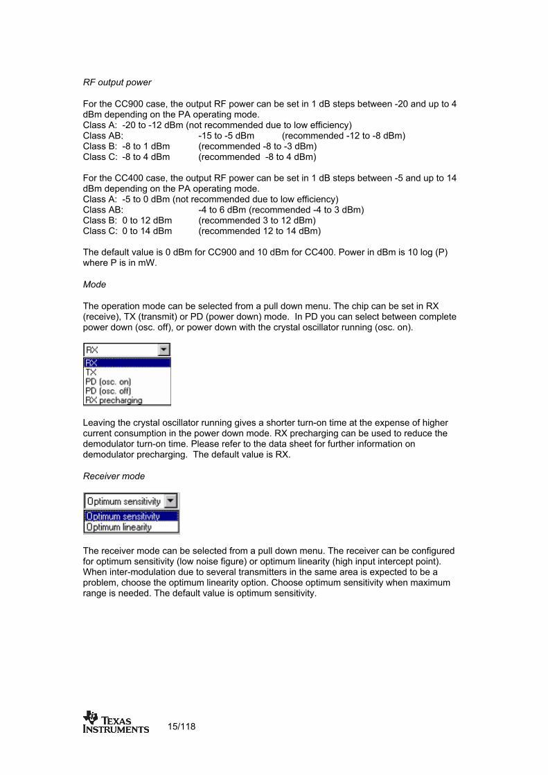
Mode
The operation mode can be selected from a pull down menu. The chip can be set in RX (receive), TX (transmit) or PD (power down) mode. In PD you can select between complete power down (osc. off), or power down with the crystal oscillator running (osc. on).
Leaving the crystal oscillator running gives a shorter turn-on time at the expense of higher current consumption in the power down mode. RX precharging can be used to reduce the demodulator turn-on time. Please refer to the data sheet for further information on demodulator precharging. The default value is RX.
Receiver mode
The receiver mode can be selected from a pull down menu. The receiver can be configured for optimum sensitivity (low noise figure) or optimum linearity (high input intercept point). When inter-modulation due to several transmitters in the same area is expected to be a problem, choose the optimum linearity option. Choose optimum sensitivity when maximum range is needed. The default value is optimum sensitivity.
15/118
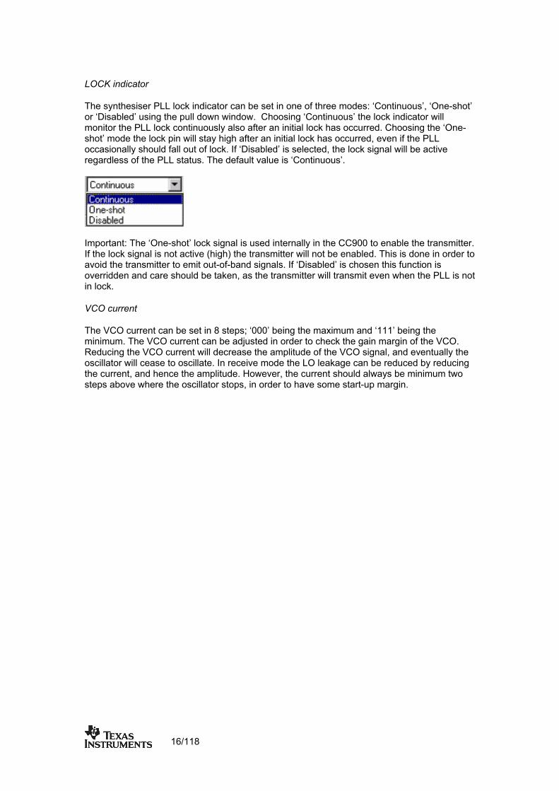
LOCK indicator
The synthesiser PLL lock indicator can be set in one of three modes: ‘Continuous’, ‘One-shot’ or ‘Disabled’ using the pull down window. Choosing ‘Continuous’ the lock indicator will monitor the PLL lock continuously also after an initial lock has occurred. Choosing the ‘One-shot’ mode the lock pin will stay high after an initial lock has occurred, even if the PLL occasionally should fall out of lock. If ‘Disabled’ is selected, the lock signal will be active regardless of the PLL status. The default value is ‘Continuous’.
Important: The ‘One-shot’ lock signal is used internally in the CC900 to enable the transmitter. If the lock signal is not active (high) the transmitter will not be enabled. This is done in order to avoid the transmitter to emit out-of-band signals. If ‘Disabled’ is chosen this function is overridden and care should be taken, as the transmitter will transmit even when the PLL is not in lock.
VCO current
The VCO current can be set in 8 steps; ‘000’ being the maximum and ‘111’ being the minimum. The VCO current can be adjusted in order to check the gain margin of the VCO. Reducing the VCO current will decrease the amplitude of the VCO signal, and eventually the oscillator will cease to oscillate. In receive mode the LO leakage can be reduced by reducing the current, and hence the amplitude. However, the current should always be minimum two steps above where the oscillator stops, in order to have some start-up margin.
16/118
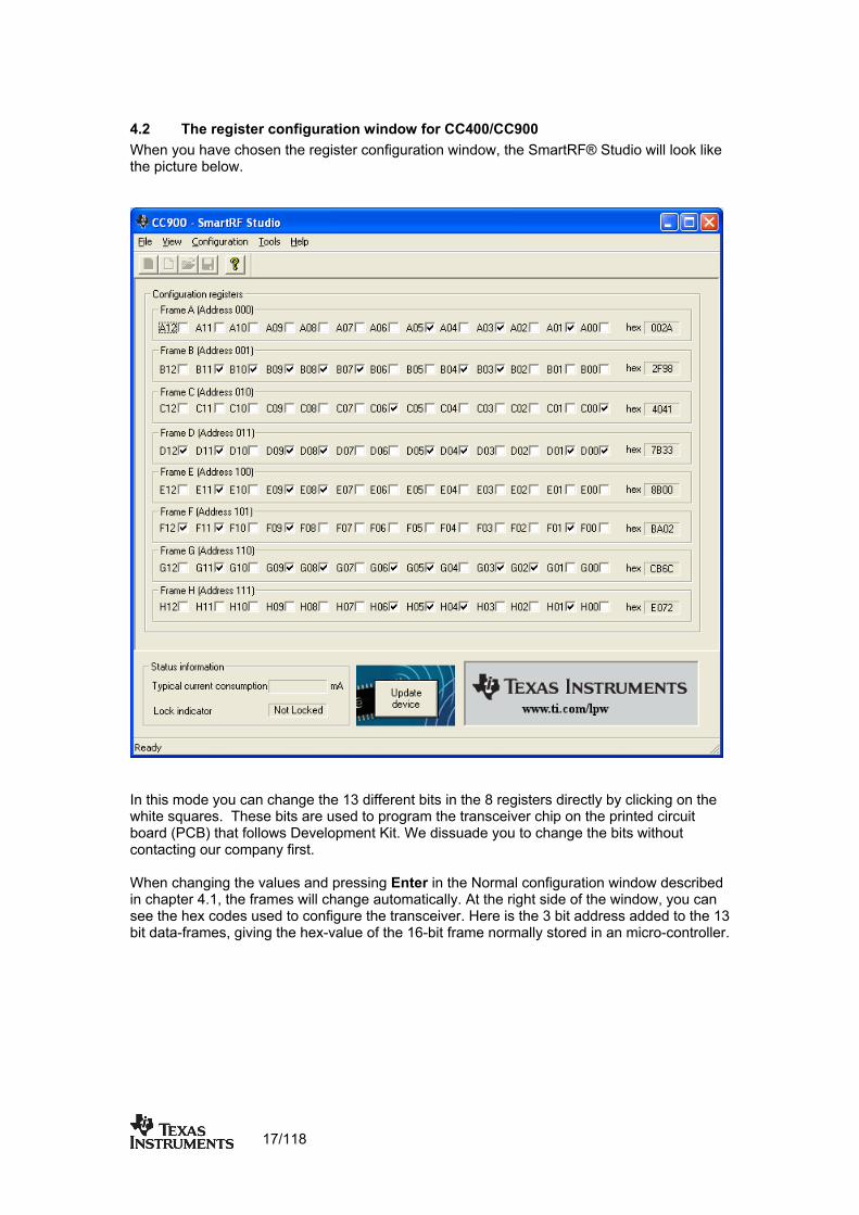
4.2 The register configuration window for CC400/CC900 When you have chosen the register configuration window, the SmartRF® Studio will look like the picture below.
In this mode you can change the 13 different bits in the 8 registers directly by clicking on the white squares. These bits are used to program the transceiver chip on the printed circuit board (PCB) that follows Development Kit. We dissuade you to change the bits without contacting our company first. When changing the values and pressing Enter in the Normal configuration window described in chapter 4.1, the frames will change automatically. At the right side of the window, you can see the hex codes used to configure the transceiver. Here is the 3 bit address added to the 13 bit data-frames, giving the hex-value of the 16-bit frame normally stored in an micro-controller.
17/118

4.3 Description of the Tools for CC400/CC900 Tools in the SmartRF® Studio are small independent software programs that are accessible from the Tools menu.
4.3.1 Programming It is possible to program the microcontroller on the Demonstration Board for the CC400 and the CC900 from SmartRF® Studio. Selecting Programming in the Tools menu (Alt+T+P) open a new window tool for this demonstration board programming. This window is as shown below.
The interface communicates with the Evaluation Board. Before programming can start, you must plug the Demonstration Board into the edge connector on the CC400/900 Evaluation Board. The software will inform you if you have not installed the Demonstration Board correctly on the demonstrator before programming. Please see the User Manuals for the Development Kit for details regarding the Evaluation Board and Demonstration Board. Before programming the demonstration board the battery should be removed, because the Evaluation board gives power to the MCU during programming.
18/118
4.3.2 EEPROM-programming The register setting for the transceivers is stored in the EEPROM of the microcontroller. The idea is that the user can change the settings of the transceivers on the demonstrator by changing the data in the EEPROM. Before you can program the EEPROM, you must load valid data into the EEPROM-buffer. This can be done by either using the default setting, load from file or read from board. If default setting is selected, then the EEPROM-buffer is filled with default values that correspond to the data in the demonstration board when you got it. This is a proper selection when you want to go back to the recommended settings after testing the demonstrator using other settings. To use the correct default setting for the demonstrator board, the user must ensure that the selected device in SmartRF® Studio is the same as the transceiver on the demonstration board. If CC400 is selected the default setting is according to the EEPROM setting given in CC400DBK User Manual, and if CC900 is selected the default setting is according to the EEPROM setting given in CC900DBK User Manual. If CC1000 is selected before the programming tool is opened, the default setting radio button will not give a default setting, because we have for the moment not implemented a demonstrator for CC1000. If from file is selected, then the load and the save buttons are enabled. Here you can either load data from a file to the EEPROM-buffer, or save the EEPROM-buffer to a file. There are two types of files that are allowed to load. That is the *.eep and *.txt. The eep-format is the normal file type for the EEPROM data. The txt-file is the text-file that is generated under SmartRF® Studio when print register to file is selected in Normal View. If another text-file is loaded an error message will open. When saving the buffer to a file, the format will be of *.eep. If from board is selected, then the read and save buttons are enabled. By clicking on this button, the software starts to read the EEPROM of the connected demonstration board, into the EEPROM-buffer. The Progress bar at the bottom of the EEPROM-programming frame starts to go, and indicate the progress of the reading. An error message will open if no demonstrator is connected to the evaluation board. The buffer data can now be used to either program to another board or store to a *.eep file. When the EEPROM-buffer contains useful data, the program EEPROM button is enabled. This button writes the data from the EEPROM-buffer to the EEPROM of the microcontroller. The Progress bar at the bottom of the EEPROM-programming frame indicates the progress of the programming. An error message will be shown if no demonstrator is connected to the evaluation board.
19/118
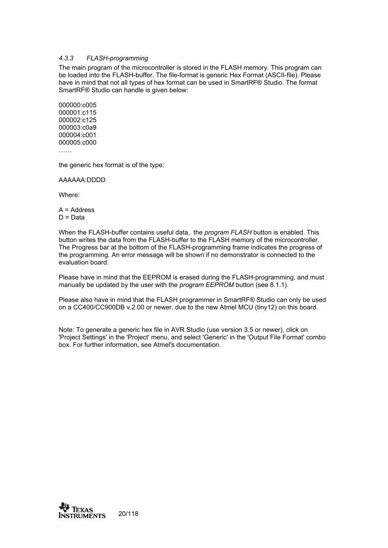
4.3.3 FLASH-programming The main program of the microcontroller is stored in the FLASH memory. This program can be loaded into the FLASH-buffer. The file-format is generic Hex Format (ASCII-file). Please have in mind that not all types of hex format can be used in SmartRF® Studio. The format SmartRF® Studio can handle is given below: 000000:c005 000001:c115 000002:c125 000003:c0a9 000004:c001 000005:c000 …… the generic hex format is of the type: AAAAAA:DDDD Where: A = Address D = Data When the FLASH-buffer contains useful data, the program FLASH button is enabled. This button writes the data from the FLASH-buffer to the FLASH memory of the microcontroller. The Progress bar at the bottom of the FLASH-programming frame indicates the progress of the programming. An error message will be shown if no demonstrator is connected to the evaluation board. Please have in mind that the EEPROM is erased during the FLASH-programming, and must manually be updated by the user with the program EEPROM button (see 8.1.1). Please also have in mind that the FLASH programmer in SmartRF® Studio can only be used on a CC400/CC900DB v.2.00 or newer, due to the new Atmel MCU (tiny12) on this board. Note: To generate a generic hex file in AVR Studio (use version 3.5 or newer), click on 'Project Settings' in the 'Project' menu, and select 'Generic' in the 'Output File Format' combo box. For further information, see Atmel's documentation.
20/118

5. SmartRF® Studio for CC1000 The CC1000 has two configuration views. The parameter entry screen is the default window and can be chosen by pressing F2 or selecting Normal from the View menu. In this window you can change the system parameters, get status information and component values. The other configuration window is the “register” configuration, which is selected by pressing F3 or selecting Register from the View menu. It gives you the possibility to change the bits in the configuration registers directly. This window is mainly used to give additional information and we dissuade you to change the bits. To send the configuration data to the transceiver chip, press F5 or select Update Device from the Configuration menu or press the Update device button at the bottom of the screen. Note: When pressing Enter the parameters will be checked and component values will be calculated, but the transceiver will not be programmed until Update device is activated.
21/118
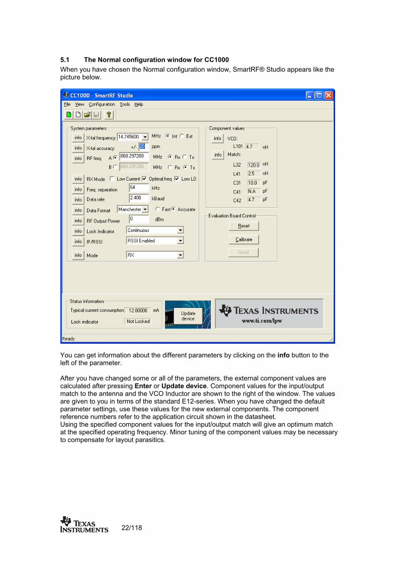
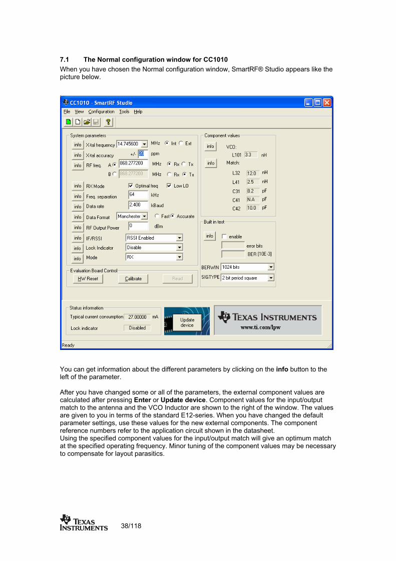
5.1 The Normal configuration window for CC1000 When you have chosen the Normal configuration window, SmartRF® Studio appears like the picture below.
You can get information about the different parameters by clicking on the info button to the left of the parameter. After you have changed some or all of the parameters, the external component values are calculated after pressing Enter or Update device. Component values for the input/output match to the antenna and the VCO Inductor are shown to the right of the window. The values are given to you in terms of the standard E12-series. When you have changed the default parameter settings, use these values for the new external components. The component reference numbers refer to the application circuit shown in the datasheet. Using the specified component values for the input/output match will give an optimum match at the specified operating frequency. Minor tuning of the component values may be necessary to compensate for layout parasitics.
22/118
5.1.1 System parameters This chapter describes the different parameters and the options you have when changing them.
Crystal frequency
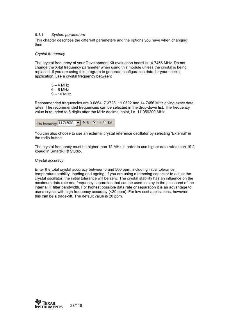
The crystal frequency of your Development Kit evaluation board is 14.7456 MHz. Do not change the X-tal frequency parameter when using this module unless the crystal is being replaced. If you are using this program to generate configuration data for your special application, use a crystal frequency between: 3 – 4 MHz 6 – 8 MHz 9 – 16 MHz Recommended frequencies are 3.6864, 7.3728, 11.0592 and 14.7456 MHz giving exact data rates. The recommended frequencies can be selected in the drop-down list. The frequency value is rounded to 6 digits after the MHz decimal point, i.e. 11.059200 MHz.
You can also choose to use an external crystal reference oscillator by selecting ‘External’ in the radio button. The crystal frequency must be higher than 12 MHz in order to use higher data rates than 19.2 kbaud in SmartRF® Studio.
Crystal accuracy
Enter the total crystal accuracy between 0 and 500 ppm, including initial tolerance, temperature stability, loading and ageing. If you are using a trimming capacitor to adjust the crystal oscillator, the initial tolerance will be zero. The crystal stability has an influence on the maximum data rate and frequency separation that can be used to stay in the passband of the internal IF filter bandwidth. For highest possible data rate or separation it is an advantage to use a crystal with high frequency accuracy (<20 ppm). For low cost applications, however, this can be a trade-off. The default value is 20 ppm.
23/118

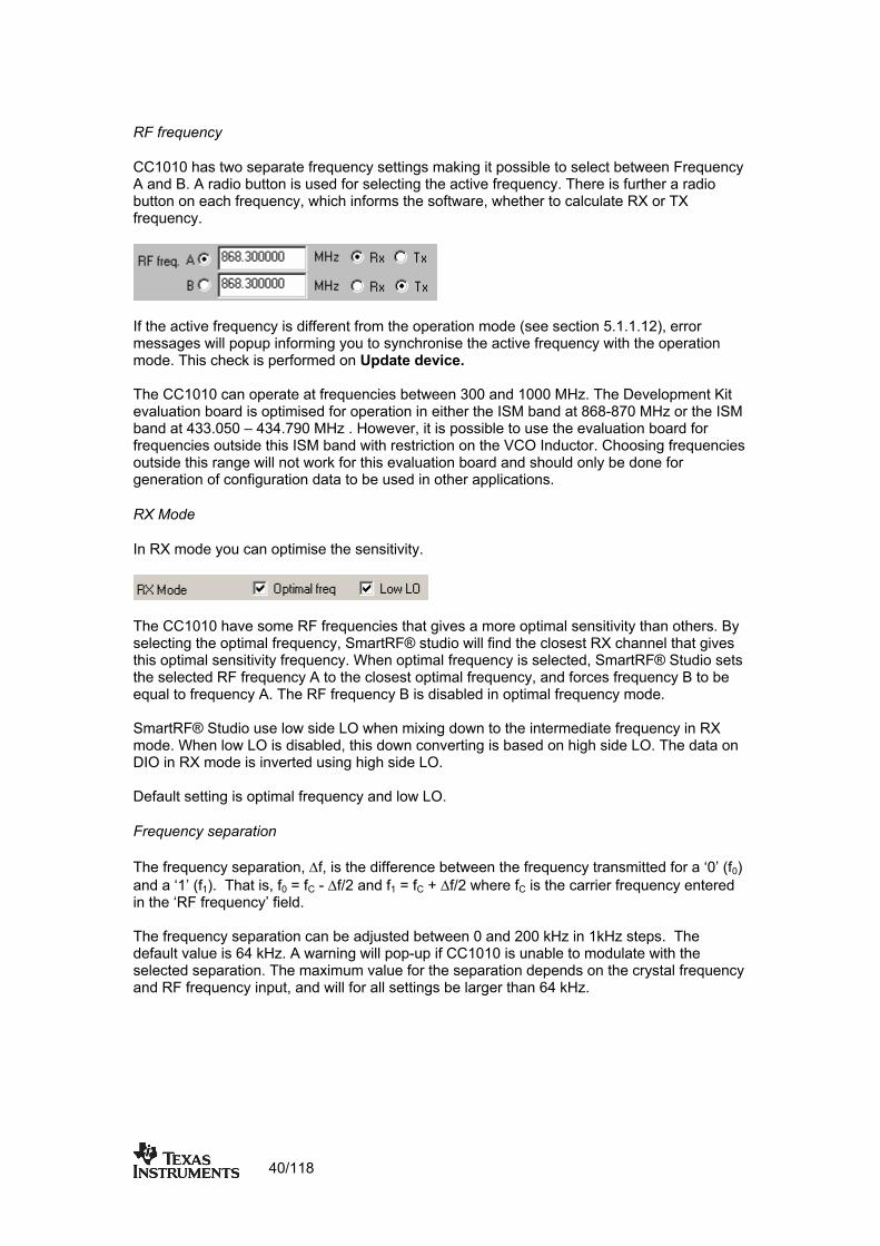
RF frequency
CC1000 has two separate frequency settings making it possible to select between Frequency A and B. A radio button is used for selecting the active frequency. There is further a radio button on each frequency, which informs the software, whether to calculate RX or TX frequency.
If the active frequency is different from the operation mode (see section 5.1.1.12), error messages will popup informing you to synchronise the active frequency with the operation mode. The CC1000 can operate at frequencies between 300 and 1000 MHz. The Development Kit evaluation board is optimised for operation in either the ISM band at 868-870 MHz or the ISM band at 433.050 – 434.790 MHz . However, it is possible to use the evaluation board for frequencies outside this ISM band with restriction on the VCO Inductor. Choosing frequencies outside this range will not work for this evaluation board and should only be done for generation of configuration data to be used in other applications.
RX Mode
In RX mode you can optimise the sensitivity and current consumption.
The CC1000 have some RF frequencies that gives a more optimal sensitivity than others. By selecting the optimal frequency, SmartRF® studio will find the closest RX channel that gives this optimal sensitivity frequency. When optimal frequency is selected, SmartRF® Studio sets the selected RF frequency A to the closest optimal frequency, and forces frequency B to be equal to frequency A. The RF frequency B is disabled in optimal frequency mode. SmartRF® Studio use low side LO when mixing down to the intermediate frequency in RX mode. When low LO is disabled, this down converting is based on high side LO. The data on DIO in RX mode is inverted using high side LO. In order to use CC1000 in a battery operation system, it is important to reduce the current consumption in RX mode. By activating the Low Current consumption, the current consumption in RX mode is reduced. The sensitivity will drop 1-2 dB when the low current mode is used. Default setting is low current and optimal frequency.
24/118

Frequency separation
The frequency separation, ∆f, is the difference between the frequency transmitted for a ‘0’ (f0) and a ‘1’ (f1). That is, f0 = fC - ∆f/2 and f1 = fC + ∆f/2 where fC is the carrier frequency entered in the ‘RF frequency’ field. The frequency separation can be adjusted between 0 and 200 kHz in 1kHz steps. The default value is 64 kHz. A warning will pop-up if CC1000 is unable to modulate with the selected separation. The maximum value for the separation depends on the crystal frequency and RF frequency input, and will for all settings be larger than 64 kHz.
Data rate
The data rate can be set between 0.3 and 76.8 kbaud. The default setting is 2.4 kbaud. If synchronous mode and recommended crystal frequencies is selected, SmartRF® Studio will find the closest accurate data rate. If synchronous mode is selected without using recommended crystal frequencies, a warning will pop-up informing you that the data rate will differ from the one given in the Data rate input. To get a higher data rate then 19.2 kbaud, the crystal frequency must be higher than 12 MHz in SmartRF® Studio. If the selected recommended frequency is 3.6864, 7.3728 or 11.0592 MHz in synchronous mode the maximum data rate is forced down to 19.2 kbaud (a pop-up message will inform the user). For a 14.745600 MHz crystal however the data rate is rounded to the closest accurate data rate up to 76.8 kbaud.
25/118

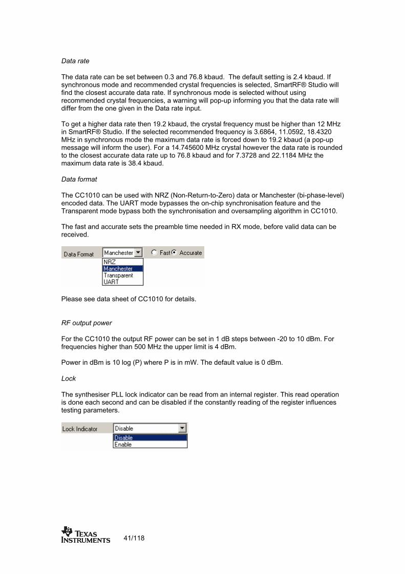
Data format
The CC1000 can be used with NRZ (Non-Return-to-Zero) data or Manchester (bi-phase-level) encoded data. The UART mode bypasses the on-chip synchronisation feature in CC1000. The fast and accurate sets the preamble time needed in RX mode, before valid data can be received.
Please see data sheet of CC1000 for details.
RF output power
For the CC1000 the output RF power can be set in 1 dB steps between -20 to 10 dBm. For frequencies higher than 500 MHz the upper limit is 5 dBm. Power in dBm is 10 log (P) where P is in mW. The default value is 0 dBm.
Lock
The synthesiser PLL lock indicator can be set in one of three modes: ‘Continuous’, ‘One-shot’ or ‘Disabled’ using the pull down window. Choosing ‘Continuous’ the lock indicator will monitor the PLL lock continuously also after an initial lock has occurred. Choosing the ‘One-shot’ mode the CHP_OUT (lock) pin will stay high after an initial lock has occurred, even if the PLL occasionally should fall out of lock. If ‘Disabled’ is selected, the lock signal will not be sent to the CHP_OUT pin to give PLL status. ‘External PA control’ is selected if an external Power Amplifier is needed, and ‘External LNA control’ is selected if an external LNA is needed. The CHP_OUT pin can then control the external LNA/PA, based on the setting of the TX_PD and RX_PD in the MAIN register of CC1000. Please see datasheet for details. The default value is ‘Continuous’. Important: The ‘One-shot’ lock signal is used internally in the CC1000 to enable the transmitter. If the lock signal is not active (high) the transmitter will not be enabled. This is in order to avoid the transmitter to emit out-of-band signals. If ‘Disabled’ is chosen this function is overridden and care should be taken, as the transmitter will transmit even when the PLL is not in lock.
26/118
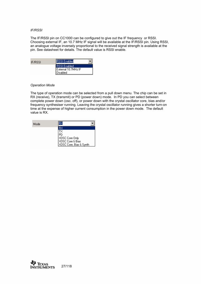
IF/RSSI
The IF/RSSI pin on CC1000 can be configured to give out the IF frequency or RSSI. Choosing external IF, an 10.7 MHz IF signal will be available at the IF/RSSI pin. Using RSSI, an analogue voltage inversely proportional to the received signal strength is available at the pin. See datasheet for details. The default value is RSSI enable.
Operation Mode
The type of operation mode can be selected from a pull down menu. The chip can be set in RX (receive), TX (transmit) or PD (power down) mode. In PD you can select between complete power down (osc. off), or power down with the crystal oscillator core, bias and/or frequency synthesiser running. Leaving the crystal oscillator running gives a shorter turn-on time at the expense of higher current consumption in the power down mode. The default value is RX.
27/118
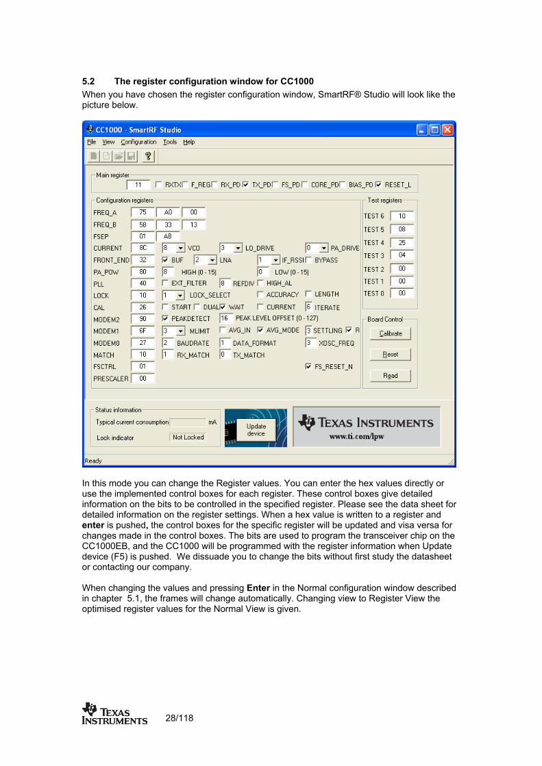
5.2 The register configuration window for CC1000 When you have chosen the register configuration window, SmartRF® Studio will look like the picture below.
In this mode you can change the Register values. You can enter the hex values directly or use the implemented control boxes for each register. These control boxes give detailed information on the bits to be controlled in the specified register. Please see the data sheet for detailed information on the register settings. When a hex value is written to a register and enter is pushed, the control boxes for the specific register will be updated and visa versa for changes made in the control boxes. The bits are used to program the transceiver chip on the CC1000EB, and the CC1000 will be programmed with the register information when Update device (F5) is pushed. We dissuade you to change the bits without first study the datasheet or contacting our company. When changing the values and pressing Enter in the Normal configuration window described in chapter 5.1, the frames will change automatically. Changing view to Register View the optimised register values for the Normal View is given.
28/118
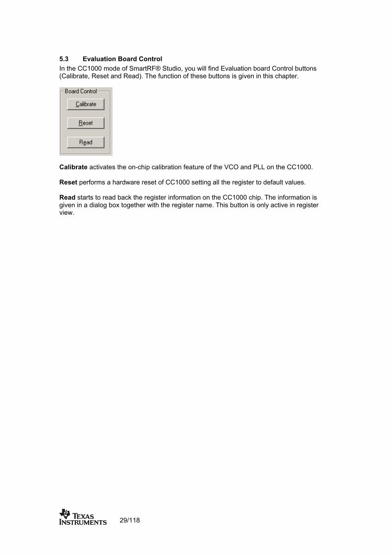
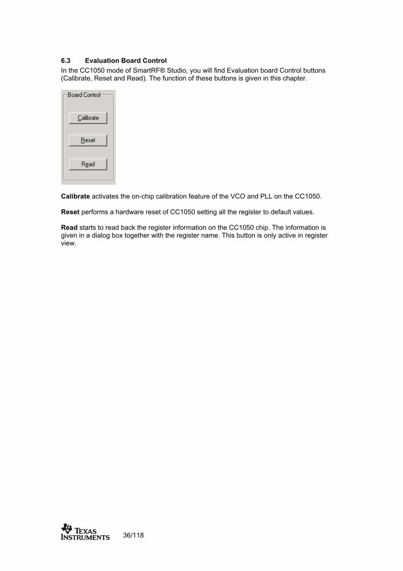
5.3 Evaluation Board Control In the CC1000 mode of SmartRF® Studio, you will find Evaluation board Control buttons (Calibrate, Reset and Read). The function of these buttons is given in this chapter.
Calibrate activates the on-chip calibration feature of the VCO and PLL on the CC1000. Reset performs a hardware reset of CC1000 setting all the register to default values. Read starts to read back the register information on the CC1000 chip. The information is given in a dialog box together with the register name. This button is only active in register view.
29/118
6. SmartRF® Studio for CC1050 The CC1050 has two configuration views. The parameter entry screen is the default window and can be chosen by pressing F2 or selecting Normal from the View menu. In this window you can change the system parameters, get status information and component values. The other configuration window is the “register” configuration, which is selected by pressing F3 or selecting Register from the View menu. It gives you the possibility to change the bits in the configuration registers directly. This window is mainly used to give additional information and we dissuade you to change the bits. To send the configuration data to the transmitter chip, press F5 or select Update Device from the Configuration menu or press the Update device button at the bottom of the screen. Note: When pressing Enter the parameters will be checked and component values will be calculated, but the transmitter will not be programmed until Update device is activated.
30/118
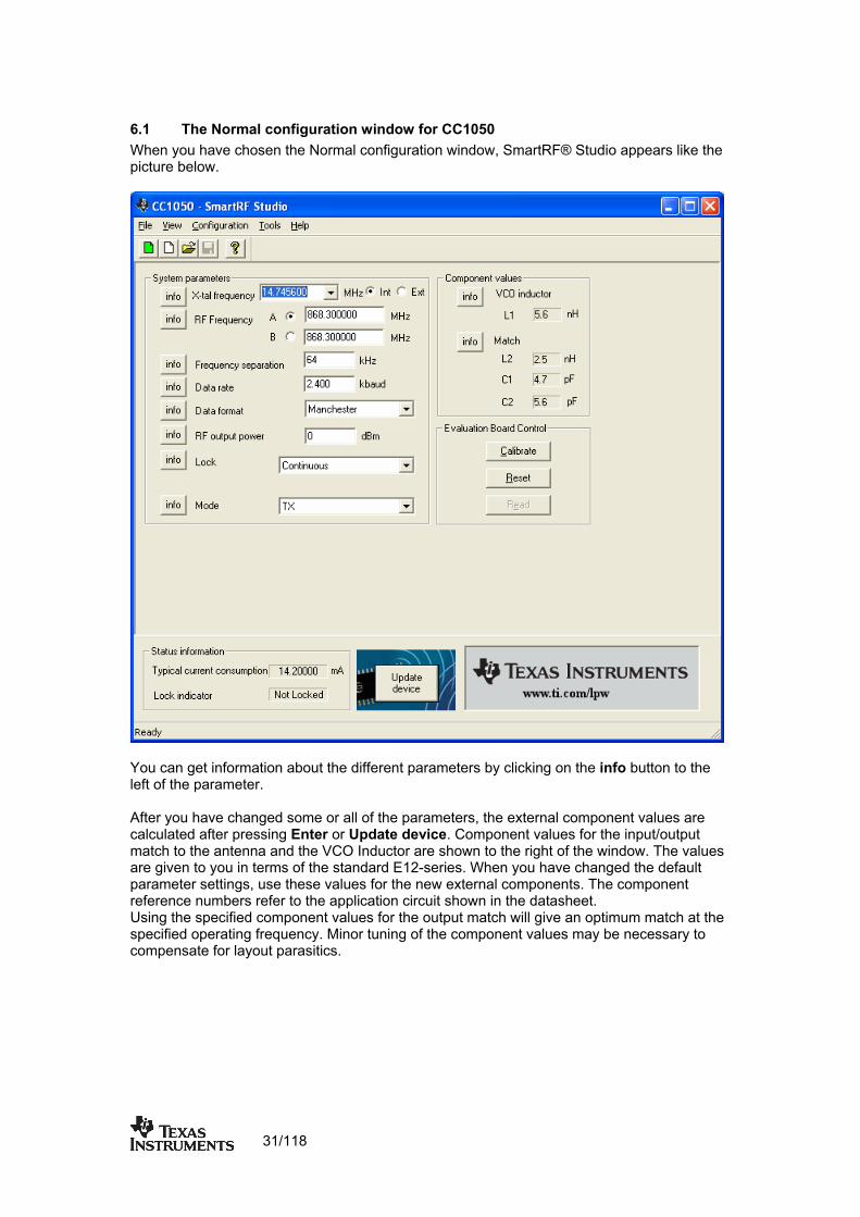
6.1 The Normal configuration window for CC1050 When you have chosen the Normal configuration window, SmartRF® Studio appears like the picture below.
You can get information about the different parameters by clicking on the info button to the left of the parameter. After you have changed some or all of the parameters, the external component values are calculated after pressing Enter or Update device. Component values for the input/output match to the antenna and the VCO Inductor are shown to the right of the window. The values are given to you in terms of the standard E12-series. When you have changed the default parameter settings, use these values for the new external components. The component reference numbers refer to the application circuit shown in the datasheet. Using the specified component values for the output match will give an optimum match at the specified operating frequency. Minor tuning of the component values may be necessary to compensate for layout parasitics.
31/118
6.1.1 System parameters This chapter describes the different parameters and the options you have when changing them.
Crystal frequency
The crystal frequency of your Development Kit evaluation board is 14.7456 MHz. Do not change the X-tal frequency parameter when using this module unless the crystal is being replaced. If you are using this program to generate configuration data for your special application, use a crystal frequency between: 3 – 4 MHz 6 – 8 MHz 9 – 16 MHz Recommended frequencies are 3.6864, 7.3728, 11.0592 and 14.7456 MHz giving exact data rates. The recommended frequencies can be selected in the drop-down list. The frequency value is rounded to 6 digits after the MHz decimal point, i.e. 11.059200 MHz.
You can also choose to use an external crystal reference oscillator by selecting ‘External’ in the radio button.
RF frequency
CC1050 has two separate frequency settings making it possible to select between Frequency A and B. A radio button is used for selecting the active frequency.
The CC1050 can operate at frequencies between 300 and 1000 MHz. The Development Kevaluation board is optimised for operation in either the ISM band at 868-870 MHz or the ISM band at 433.050 – 434.790 MHz . However, it is possible to use the evaluation board frequencies outside this ISM band with restriction on the VCO Ind
it
for uctor. Choosing frequencies
outside this range will not work for this evaluation board and should only be done for generation of configuration data to be used in other applications.
32/118
Frequency separation
The frequency separation, ∆f, is the difference between the frequency transmitted for a ‘0’ (f0) and a ‘1’ (f1). That is, f0 = fC - ∆f/2 and f1 = fC + ∆f/2 where fC is the carrier frequency entered in the ‘RF frequency’ field. The frequency separation can be adjusted between 0 and 200 kHz in 1 kHz steps. The default value is 64 kHz. A warning will pop-up if CC1050 are unable to modulate with the selected separation. The maximum value for the separation depends on the crystal frequency and RF frequency input, and will for all settings be larger than 64 kHz.
Data rate
The data rate can be set between 0.6 and 76.8 kbaud. The default setting is 2.4 kbaud. If synchronous mode and recommended crystal frequencies is selected, SmartRF® Studio will find the closest accurate data rate. If synchronous mode is selected without using recommended crystal frequencies, a warning will pop-up informing you that the data rate will differ from the one given in the Data rate input.
Data format
The CC1050 can be used with NRZ (Non-Return-to-Zero) data or Manchester (bi-phase-level) encoded data. The UART mode bypasses the on-chip synchronisation feature in CC1050.
Please see data sheet of CC1050 for details.
RF output power
For the CC1050 the output RF power can be set in 1 dB steps between -20 to 12 dBm. For frequencies higher than 500 MHz the upper limit is 8 dBm. Power in dBm is 10 log (P) where P is in mW. The default value is 0dBm.
33/118
Lock
The synthesiser PLL lock indicator can be set in one of three modes: ‘Continuous’, ‘One-shot’ or ‘Disabled’ using the pull down window. Choosing ‘Continuous’ the lock indicator will monitor the PLL lock continuously also after an initial lock has occurred. Choosing the ‘One-hot’ mode the CHP_OUT (los ck) pin will stay high after an initial lock has occurred, even if the
ot be
e ‘One-shot’ lock signal is used internally in the CC1050 to enable the itter. If the lock signal is not active (high) the transmitter will not be enabled. This is in
the transmitter to emit out-of-band signals. If ‘Disabled’ is chosen this function
n mode can be selected from a pull down menu. The chip can be set in TX (transmit) or PD (power down) mode. In PD you can select between complete power down (osc. off), or power down with the crystal oscillator core, bias and/or frequency synthesiser running. Leaving the crystal oscillator running gives a shorter turn-on time at the expense of higher current consumption in the power down mode. The default value is TX.
PLL occasionally should fall out of lock. If ‘Disabled’ is selected, the lock signal will nsent to the CHP_OUT pin to give PLL status. ‘External PA control’ is selected if an external Power Amplifier is needed. The CHP_OUT pin can then control the external PA, based on thesetting of the TX_PD in the MAIN register of CC1050. Please see datasheet for details. The default value is ‘Continuous’. Important: Thtransmorder to avoidis overridden and care should be taken, as the transmitter will transmit even when the PLL isnot in lock.
Mode
The type of operatio
34/118
6.2 The register configuration window for CC1050 When you have chosen the register configuration window, SmartRF® Studio will look like the picture below.
In this mode you can change the Register values. You can enter the hex values directly or use the implemented control boxes for each register. These control boxes give detailed information on the bits to be controlled in the specified register. Please see the data sheet for detailed information on the register settings. When a hex value is written to a register and enter is pushed, the control boxes for the specific register will be updated and visa versa for changes made in the control boxes. The bits are used to program the transmitter chip on the CC1050EB, and the CC1050 will be programmed with the register information when Update device (F5) is pushed. We dissuade you to change the bits without first study the datasheet or contacting our company. When changing the values and pressing Enter in the Normal configuration window described in chapter 6.1, the frames will change automatically. Changing view to Register View the optimised register values for the Normal View is given.
35/118
6.3 Evaluation Board Control In the CC1050 mode of SmartRF® Studio, you will find Evaluation board Control buttons (Calibrate, Reset and Read). The function of these buttons is given in this chapter.
Calibrate activates the on-chip calibration feature of the VCO and PLL on the CC1050. Reset performs a hardware reset of CC1050 setting all the register to default values. Read starts to read back the register information on the CC1050 chip. The information is given in a dialog box together with the register name. This button is only active in register view.
36/118
7. SmartRF® Studio for CC1010 The CC1010 has two configuration views. The parameter entry screen is the default window and can be chosen by pressing F2 or selecting Normal from the View menu. In this window you can change the system parameters, get status information and component values. The other configuration window is the “register” configuration, which is selected by pressing F3 or selecting Register from the View menu. It gives you the possibility to change the bits in the configuration registers directly. This window is mainly used to give additional information and we dissuade you to change the bits. To send the configuration data to the transceiver chip, press F5 or select Update Device from the Configuration menu or press the Update device button at the bottom of the screen. In order to configure the CC1010EB, you first need an embedded software (SmartRF®_adapter.hex) inside CC1010 that communicate with the SmartRF® Studio. SmartRF® Studio will check the embedded software the first time Update device is activated. If the CC1010 embedded software differs from the required software (SmartRF_adapter.hex), a programming application (ccprog.exe) will be activated, allowing the user to configure CC1010 with the software SmartRF®_adapter.hex. The user only need to click on the Do it button in order to update the CC1010 core with the required embedded software. After verifying the programming the user can exit this programming window and work with the SmartRF® Studio window. For additional information regarding the programming application (ccprog.exe), please study the IDE User Manual. Note: When pressing Enter the parameters will be checked and component values will be calculated, but the transceiver will not be programmed until Update device is activated.
37/118
7.1 The Normal configuration window for CC1010 When you have chosen the Normal configuration window, SmartRF® Studio appears like the picture below.
You can get information about the different parameters by clicking on the info button to the left of the parameter. After you have changed some or all of the parameters, the external component values are calculated after pressing Enter or Update device. Component values for the input/output match to the antenna and the VCO Inductor are shown to the right of the window. The values are given to you in terms of the standard E12-series. When you have changed the default parameter settings, use these values for the new external components. The component reference numbers refer to the application circuit shown in the datasheet. Using the specified component values for the input/output match will give an optimum match at the specified operating frequency. Minor tuning of the component values may be necessary to compensate for layout parasitics.
38/118
7.1.1 System parameters This chapter describes the different parameters and the options you have when changing them.
Crystal frequency
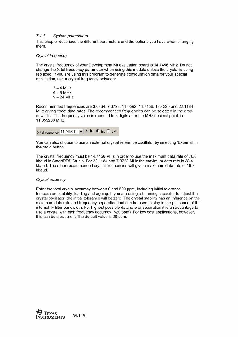
The crystal frequency of your Development Kit evaluation board is 14.7456 MHz. Do not change the X-tal frequency parameter when using this module unless the crystal is being replaced. If you are using this program to generate configuration data for your special application, use a crystal frequency between: 3 – 4 MHz 6 – 8 MHz 9 – 24 MHz Recommended frequencies are 3.6864, 7.3728, 11.0592, 14.7456, 18.4320 and 22.1184 MHz giving exact data rates. The recommended frequencies can be selected in the drop-down list. The frequency value is rounded to 6 digits after the MHz decimal point, i.e. 11.059200 MHz.
You can also choose to use an external crystal reference oscillator by selecting ‘External’ in the radio button. The crystal frequency must be 14.7456 MHz in order to use the maximum data rate of 76.8 kbaud in SmartRF® Studio. For 22.1184 and 7.3728 MHz the maximum data rate is 38.4 kbaud. The other recommended crystal frequencies will give a maximum data rate of 19.2 kbaud.
Crystal accuracy
Enter the total crystal accuracy between 0 and 500 ppm, including initial tolerance, temperature stability, loading and ageing. If you are using a trimming capacitor to adjust the crystal oscillator, the initial tolerance will be zero. The crystal stability has an influence on the maximum data rate and frequency separation that can be used to stay in the passband of the internal IF filter bandwidth. For highest possible data rate or separation it is an advantage to use a crystal with high frequency accuracy (<20 ppm). For low cost applications, however, this can be a trade-off. The default value is 20 ppm.
39/118
RF frequency
CC1010 has two separate frequency settings making it possible to select between Frequency A and B. A radio button is used for selecting the active frequency. There is further a radio button on each frequency, which informs the software, whether to calculate RX or TX frequency.
If the active frequency is different from the operation mode (see section 5.1.1.12), error
for uctor. Choosing frequencies
will not work for this evaluation board and should only be done for of configuration data to be used in other applications.
In RX mode you can optimise the sensitivity.
messages will popup informing you to synchronise the active frequency with the operation mode. This check is performed on Update device. The CC1010 can operate at frequencies between 300 and 1000 MHz. The Development Kit evaluation board is optimised for operation in either the ISM band at 868-870 MHz or the ISM band at 433.050 – 434.790 MHz . However, it is possible to use the evaluation board frequencies outside this ISM band with restriction on the VCO Indoutside this range generation
RX Mode
The CC1010 have some RF frequencies that gives a more optimal sensitivity than others. By selecting the optimal frequency, SmartRF® studio will find the closest RX channel that gives this optimal sensitivity frequency. When optimal frequency is selected, SmartRF® Studio sets
own to the intermediate frequency in RX g is based on high side LO. The data on
al frequency and low LO.
f, is the difference between the frequency transmitted for a ‘0’ (f0)
odulate with the selected separation. The maximum value for the separation depends on the crystal frequency and RF frequency input, and will for all settings be larger than 64 kHz.
the selected RF frequency A to the closest optimal frequency, and forces frequency B to be equal to frequency A. The RF frequency B is disabled in optimal frequency mode. SmartRF® Studio use low side LO when mixing dmode. When low LO is disabled, this down convertinDIO in RX mode is inverted using high side LO. Default setting is optim
Frequency separation
The frequency separation, ∆and a ‘1’ (f1). That is, f0 = fC - ∆f/2 and f1 = fC + ∆f/2 where fC is the carrier frequency entered in the ‘RF frequency’ field. The frequency separation can be adjusted between 0 and 200 kHz in 1kHz steps. The default value is 64 kHz. A warning will pop-up if CC1010 is unable to m
40/118
Data rate
The data rate can be set between 0.3 and 76.8 kbaud. The default setting is 2.4 kbaud. If synchronous mode and recommended crystal frequencies is selected, SmartRF® Studio will find the closest accurate data rate. If synchronous mode is selected without using recommended crystal frequencies, a warning will pop-up informing you that the data rate will differ from the one given in the Data rate input. To get a higher data rate then 19.2 kbaud, the crystal frequency must be higher than 12 MHz in SmartRF® Studio. If the selected recommended frequency is 3.6864, 11.0592, 18.4320 MHz in synchronous mode the maximum data rate is forced down to 19.2 kbaud (a pop-up message will inform the user). For a 14.745600 MHz crystal however the data rate is rounded to the closest accurate data rate up to 76.8 kbaud and for 7.3728 and 22.1184 MHz the maximum data rate is 38.4 kbaud.
Data format
The CC1010 can be used with NRZ (Non-Return-to-Zero) data or Manchester (bi-phase-level) encoded data. The UART mode bypasses the on-chip synchronisation feature and the Transparent mode bypass both the synchronisation and oversampling algorithm in CC1010. The fast and accurate sets the preamble time needed in RX mode, before valid data can be received.
Please see data sheet of CC1010 for details.
F output power
For the CC1010 the output RF power can be set in 1 dB steps between -20 to 10 dBm. For ncies higher than 500 MHz the upper limit is 4 dBm.
The synthesiser PLL lock indicator can be read from an internal register. This read operation is done each second and can be disabled if the constantly reading of the register influences testing parameters.
R
freque
Power in dBm is 10 log (P) where P is in mW. The default value is 0 dBm.
Lock
41/118
IF/RSSI
The AD2 pin on CC1010 can be configured to give out the IF frequency or RSSI. Choosing external IF, a 10.7 MHz IF signal will be available on the AD2 pin. Using RSSI, an analogue voltage inversely proportional to the received signal will then be available on this pin. See datasheet for details. The default value is RSSI enable.
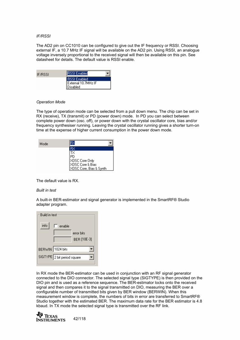
Operation Mode
The type of operation mode can be selected from a pull down menu. The chip can be set in X (receive), TX (transmit) or PD (power down) mode. In PD you can select between
complete power down (osc. off), or power down with the crystal oscillator core, bias and/or frequency synthesiser running. Leaving the crystal oscillator running gives a shorter turn-on time at the expense of higher current consumption in the power down mode.
R
uilt in test
built-in BER-estimator and signal generator is implemented in the SmartRF® Studio
The default value is RX.
B
Aadapter program.
In RX mode the BER-estimator can be used in conjunction with an RF signal generator connected to the DIO connector. The selected signal type (SIGTYPE) is then provided on the DIO pin and is used as a reference sequence. The BER-estimator locks onto the received signal and then compares it to the signal transmitted on DIO, measuring the BER over a configurable number of transmitted bits given by BER window (BERWIN). When this measurement window is complete, the numbers of bits in error are transferred to SmartRF® Studio together with the estimated BER. The maximum data rate for the BER estimator is 4.8 kbaud. In TX mode the selected signal type is transmitted over the RF link.
42/118
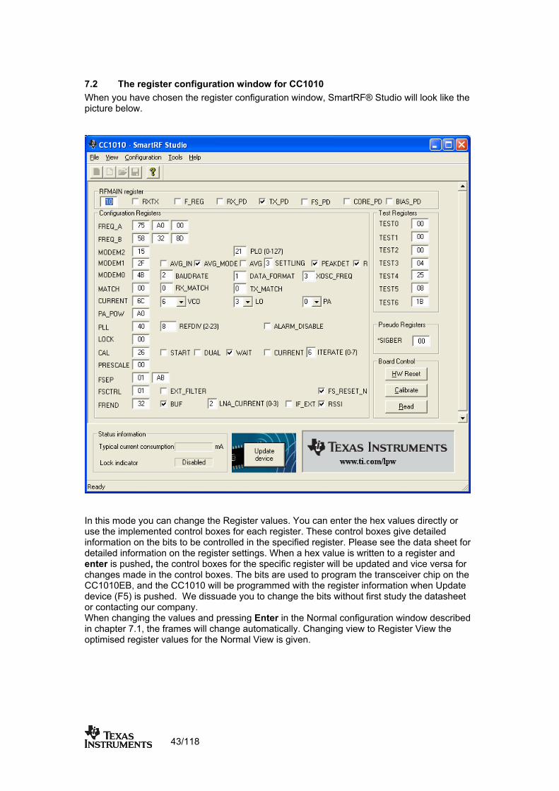
7.2 The register configuration window for CC1010 When you have chosen the register configuration window, SmartRF® Studio will look like the picture below.
In this mode you can change the Register values. You can enter the hex values directly or use the implemented control boxes for each register. These control boxes give detailed information on the bits to be controlled in the specified register. Please see the data sheet for detailed information on the register settings. When a hex value is written to a register and enter is pushed, the control boxes for the specific register will be updated and vice versa for changes made in the control boxes. The bits are used to program the transceiver chip on the CC1010EB, and the CC1010 will be programmed with the register information when Update device (F5) is pushed. We dissuade you to change the bits without first study the datasheet or contacting our company. When changing the values and pressing Enter in the Normal configuration window described in chapter 7.1, the frames will change automatically. Changing view to Register View the optimised register values for the Normal View is given.
43/118

7.3 Evaluation Board Control In the CC1010 mode of SmartRF® Studio, you will find Evaluation board Control buttons (Calibrate, Reset and Read). The function of these buttons is given in this chapter.
Calibrate activates the on-chip calibration feature of the VCO and PLL on the CC1010. HW Reset performs a hardware reset of CC1010 setting all the register to default values. Read starts to read back the register information on the CC1010 chip. The information is given in a dialog box together with the register name. This button is only active in register view.
44/118

8. SmartRF® Studio for CC102X The CC102X has two configuration views. The parameter entry screen is the default window and can be chosen by pressing F2 or selecting Normal from the View menu. In this window you can change the system parameters, get status information and component values. The other configuration window is the “register” configuration, which is selected by pressing F3 or selecting Register from the View menu. It gives you the possibility to change the bits in the configuration registers directly. This window is mainly used to give additional information and we dissuade you to change the bits. To send the configuration data to the transceiver chip, press F5 or select Update Device from the Configuration menu or press the Update device button at the bottom of the screen. Note: When pressing Enter the parameters will be checked and component values will be calculated, but the transceiver will not be programmed until Update device is activated.
45/118

8.1 The Normal configuration window for CC102X When you have chosen the Normal configuration window, SmartRF® Studio appears like the picture below.
You can get information about the different parameters by clicking on the info button to the left of the parameter. After you have changed some or all of the parameters, the external component values are calculated after pressing Enter or Update device. The values are given in terms of the standard E12-series. When you have changed the default parameter settings, use these values for the new external components. The component reference numbers refer to the application circuit shown in the datasheet and the CC102XDK User Manuals. Using the specified component values for the input/output match will give an optimum match at the specified operating frequency. Minor tuning of the component values may be necessary to compensate for layout parasitics.
46/118

8.1.1 System parameters This chapter describes the different parameters and the options you have when changing them.
Crystal frequency
The crystal frequency of your Development Kit evaluation module is 14.7456 MHz. Do not change the X-tal frequency parameter when using this module unless the crystal is being replaced. If you are using this program to generate configuration data for your special application, use a crystal frequency between: 4 - 20 MHz Recommended frequencies are 4.9152, 7.3728, 9.8304, 12.288, 14.7456, 17.2032 and 19.6608 MHz giving exact data rates. The recommended frequencies can be selected in the drop-down list. The frequency value is rounded to 6 digits after the MHz decimal point, i.e. 14.745600 MHz.
You can also choose to use an external crystal reference oscillator by selecting ‘External’ in the radio button.
internal programmable IF filter bandwidth. The default value is 5 ppm.
Crystal accuracy
Enter the total crystal accuracy between 0 and 100 ppm, including initial tolerance, temperature stability, loading and ageing. If you are using a trimming capacitor to adjust the crystal oscillator, the initial tolerance will be zero. The crystal stability has an influence on the maximum data rate and frequency separation that can be used to stay in the passband of the
47/118

RF frequency
CC102X has two separate frequency settings making it possible to select between Frequency A and B. A radio button is used for selecting the active frequency. There is further a radio button for each frequency, which informs the software, whether to calculate RX or TX frequency.
If the active frequency is different from the operation mode (see section 8.1.1.12), error messages will popup informing you to synchronise the active frequency with the operation mode. CC102X can operate at frequencies between 424 – 470 MHz and 848 - 940 MHz. Your Development Kit test module is optimised for operation in the ISM band at 868 or 433 MHz. However, it is possible to use the test module for frequencies outside this ISM band with the restriction of the external components.
Frequency separation
The frequency separation dF can be between 0 and 108 kHz at 424 – 470 MHz, and between 0 and 216 kHz at 848 – 940 MHz.. This is the difference between the frequency transmitted for a ‘0’ (F0) and a ‘1’ (F1). That is, F0 = Fc- dF/2 and F1= Fc+ dF/2, where Fc is the carrier frequency entered in the ‘RF frequency’ field. The total occupied signal bandwidth can be approximated by Carson’s rule: BW = dF + 2 Fm, where Fm is the modulation frequency. Using NRZ coding the baud rate is equal to the bit rate. Using Manchester coding the modulation frequency (in kHz) will be equal to the bit rate (in kbit/s) and the baud rate is twice the bit rate.
Data rate
The data rate can be set between 0.45 and 153.6 bBaud. Using NRZ mode, the data rate in kbits/s is equal to the Baud rate. Using Manchester code, the Baud rate is twice the bit rate. The demodulator, data slicer and bit synchroniser is optimised according to the selected data rate. In synchronous mode using recommended crystal frequencies, the data rate will be rounded to the closest accurate data rate given in the data sheet.
48/118
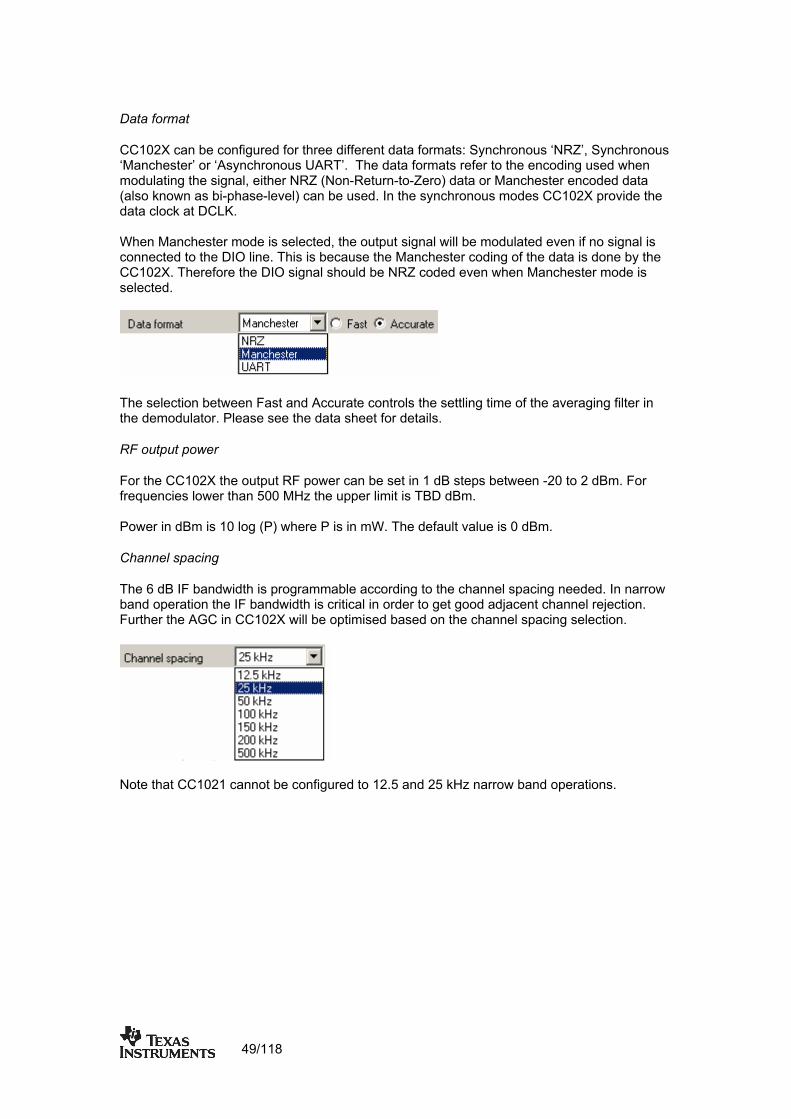
Data format
CC102X can be configured for three different data formats: Synchronous ‘NRZ’, Synchronous ‘Manchester’ or ‘Asynchronous UART’. The data formats refer to the encoding used when modulating the signal, either NRZ (Non-Return-to-Zero) data or Manchester encoded data (also known as bi-phase-level) can be used. In the synchronous modes CC102X provide the data clock at DCLK. When Manchester mode is selected, the output signal will be modulated even if no signal is connected to the DIO line. This is because the Manchester coding of the data is done by the CC102X. Therefore the DIO signal should be NRZ coded even when Manchester mode is selected.
The selection between Fast and Accurate controls the settling time of the averaging filter in
to 2 dBm. For than 500 MHz the upper limit is TBD dBm.
he 6 dB IF bandwidth is programmable according to the channel spacing needed. In narrow band operation the IF bandwidth is critical in order to get good adjacent channel rejection. Further the AGC in CC102X will be optimised based on the channel spacing selection.
the demodulator. Please see the data sheet for details.
F output power R
For the CC102X the output RF power can be set in 1 dB steps between -20 frequencies lower Power in dBm is 10 log (P) where P is in mW. The default value is 0 dBm.
Channel spacing
T
Note that CC1021 cannot be configured to 12.5 and 25 kHz narrow band operations.
49/118

Modulation
CC102X can modulate FSK, GFSK or OOK/ASK. Using GFSK the data is shaped, using a Gaussian filter before FSK modulation, in order to improve the occupied bandwidth. OOK is a type of amplitude modulation used in digital systems where the RF carrier is turned on and off in order to modulate the data.
In a fractionalthe div
-N synthesizer, spurious signals can occur at certain frequencies depending on ision ratios in the PLL. To reduce the strength of these spurs the Dithering can be
e PLL status. he LOCK pin can also be used as a Carrier Sense indicator or be set to a fixed level. In
synchronous mode the data in RX mode can be given on the LOCK pin when Data output is selected. In asynchronous mode the data output is always provided on DCLK.
enabled.
Lock
The synthesiser PLL lock indicator can be set in one of three modes: ‘Continuous’, ‘One-shot’ or ‘Disabled’. Choosing ‘Continuous’ the lock indicator will monitor the PLL lock continuously also after an initial lock have occurred. Choosing the ‘Instant’ mode the LOCK pin will stay high after an initial lock has occurred, even if the PLL occasionally should fall out of lock. If ‘Disabled’ is selected, the lock signal will be fixed to high or low regardless of thT
Note that the Lock indicator pin on CC102X is active low.
Carrier sense
he carrTle
ier sense signal is based on the RSSI value and the programmable carrier sense el. The Carrier sense signal is high as long as the RSSI is stronger than the given shold. The threshold is given by the sensitivity in RX mode and adding the carrier sense
vreth
offset.
The DCLK pin on CC102X can be used to give an interrupt signal to the MCU when the RSSI level exceeds the given threshold level. This function can be used to wake or interrupt the MCU when a strong signal is received. The DCLK Squelch enables this feature.
50/118
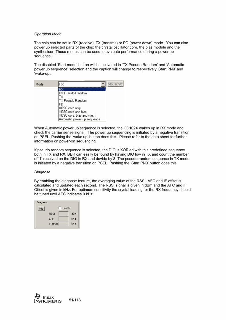
Operation Mode
The chip can be set in RX (receive), TX (transmit) or PD (power down) mode. You can also power up selected parts of the chip; the crystal oscillator core, the bias module and the synthesiser. These modes can be used to evaluate performance during a power up sequence. The disabled ‘Start mode’ button will be activated in ‘TX Pseudo Random’ and ‘Automatic power up sequence’ selection and the caption will change to respectively ‘Start PN9’ and ‘wake-up’.
When Automatic power up sequence is selected, the CC102X wakes up in RX mode and check the carrier sense signal. The power up sequencing is initiated by a negative transition on PSEL. Pushing the ‘wake up’ button does this. Please refer to the data sheet for further information on power-on sequencing. If pseudo random sequence is selected, the DIO is XOR’ed with this predefined sequence both in TX and RX. BER can easily be found by having DIO low in TX and count the number of ‘1’ received on the DIO in RX and devide by 3. The pseudo random sequence in TX mode is initiated by a negative transition on PSEL. Pushing the ‘Start PN9’ button does this.
Diagnose
By enabling the diagnose feature, the averaging value of the RSSI, AFC and IF offset is calculated and updated each second. The RSSI signal is given in dBm and the AFC and IF Offset is given in kHz. For optimum sensitivity the crystal loading, or the RX frequency should be tuned until AFC indicates 0 kHz.
51/118
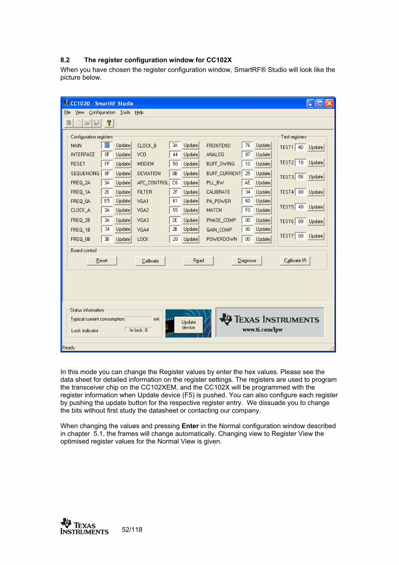
8.2 The register configuration window for CC102X When you have chosen the register configuration window, SmartRF® Studio will look like the picture below.
In this mode you can change the Register values by enter the hex values. Please see the data sheet for detailed information on the register settings. The registers are used to program the transceiver chip on the CC102XEM, and the CC102X will be programmed with the register information when Update device (F5) is pushed. You can also configure each register by pushing the update button for the respective register entry. We dissuade you to change the bits without first study the datasheet or contacting our company. When changing the values and pressing Enter in the Normal configuration window described in chapter 5.1, the frames will change automatically. Changing view to Register View the optimised register values for the Normal View is given.
52/118
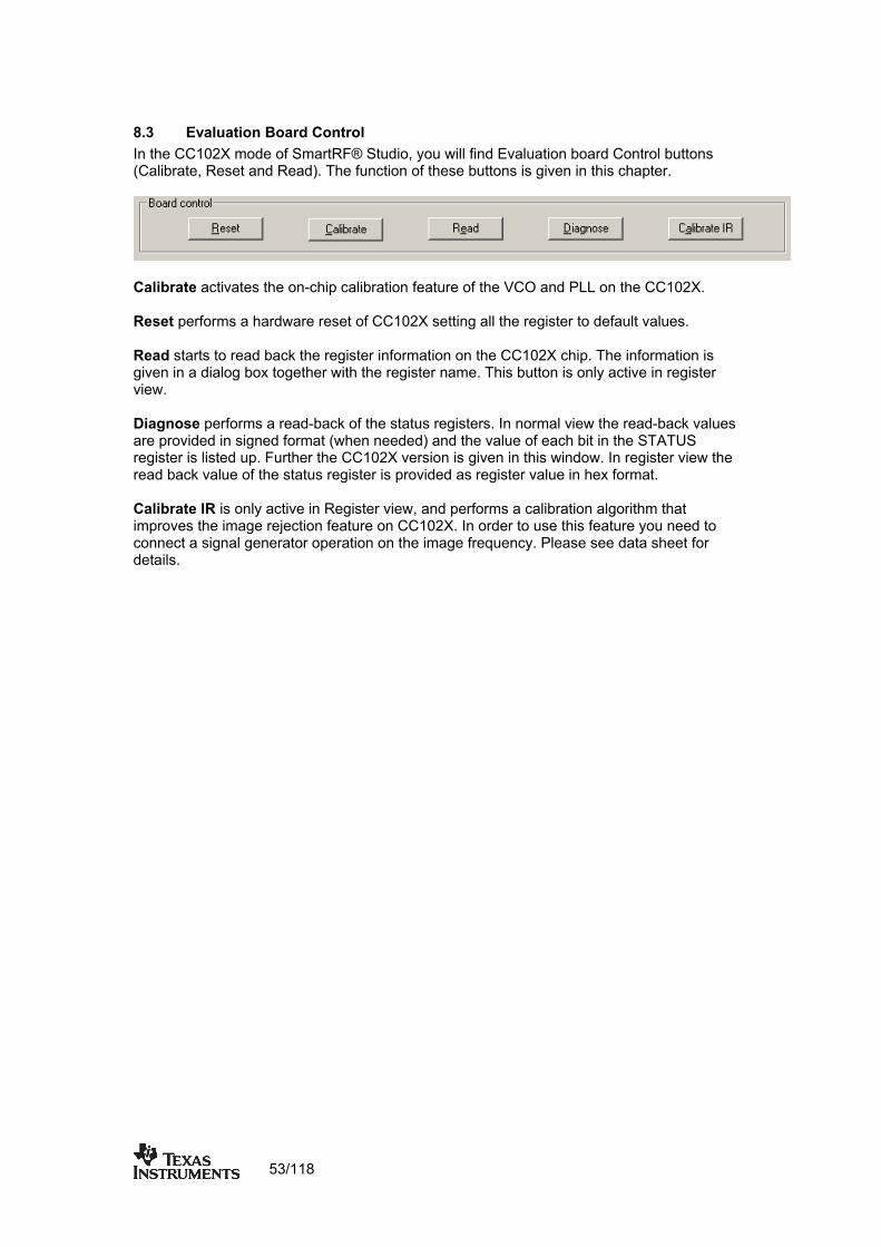
8.3 Evaluation Board Control In the CC102X mode of SmartRF® Studio, you will find Evaluation board Control buttons (Calibrate, Reset and Read). The function of these buttons is given in this chapter.
Calibrate activates the on-chip calibration feature of the VCO and PLL on the CC102X. Reset performs a hardware reset of CC102X setting all the register to default values.
er
iagnose performs a read-back of the status registers. In normal view the read-back values
e
Calibrate IR is only active in Register view, and performs a calibration algorithm that improves the image rejection feature on CC102X. In order to use this feature you need to connect a signal generator operation on the image frequency. Please see data sheet for details.
Read starts to read back the register information on the CC102X chip. The information is given in a dialog box together with the register name. This button is only active in registview. Dare provided in signed format (when needed) and the value of each bit in the STATUSregister is listed up. Further the CC102X version is given in this window. In register view thread back value of the status register is provided as register value in hex format.
53/118

9. SmartRF® Studio for CC1070 The CC1070 has two configuration views. The parameter entry screen is the default window and can be chosen by pressing F2 or selecting Normal from the View menu. In this window you can change the system parameters, get status information and component values. The other configuration window is the “register” configuration, which is selected by pressing F3 or selecting Register from the View menu. It gives you the possibility to change the bits in the configuration registers directly. This window is mainly used to give additional information and we dissuade you to change the bits. To send the configuration data to the transceiver chip, press F5 or select Update Device from the Configuration menu or press the Update device button at the bottom of the screen. Note: When pressing Enter the parameters will be checked and component values will be calculated, but the transceiver will not be programmed until Update device is activated.
54/118
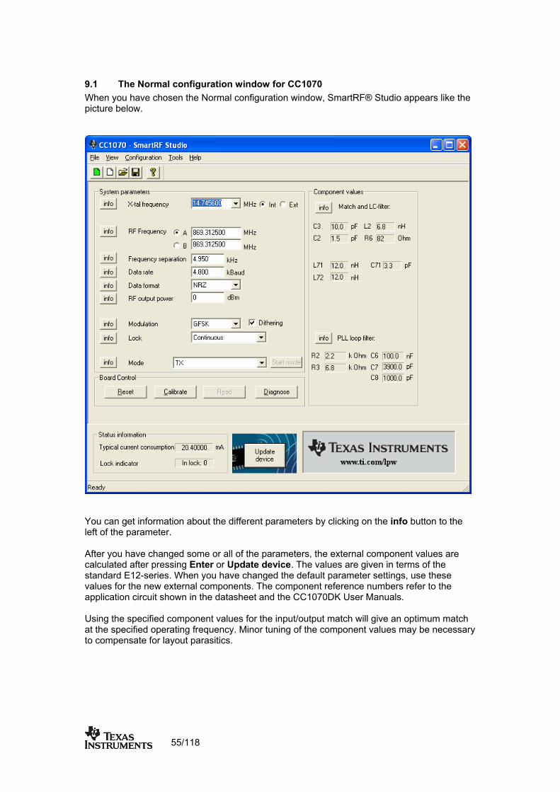
9.1 The Normal configuration window for CC1070 When you have chosen the Normal configuration window, SmartRF® Studio appears like the picture below.
You can get information about the different parameters by clicking on the info button to the left of the parameter. After you have changed some or all of the parameters, the external component values are calculated after pressing Enter or Update device. The values are given in terms of the standard E12-series. When you have changed the default parameter settings, use these values for the new external components. The component reference numbers refer to the application circuit shown in the datasheet and the CC1070DK User Manuals. Using the specified component values for the input/output match will give an optimum match at the specified operating frequency. Minor tuning of the component values may be necessary to compensate for layout parasitics.
55/118
9.1.1 System parameters This chapter describes the different parameters and the options you have when changing them.
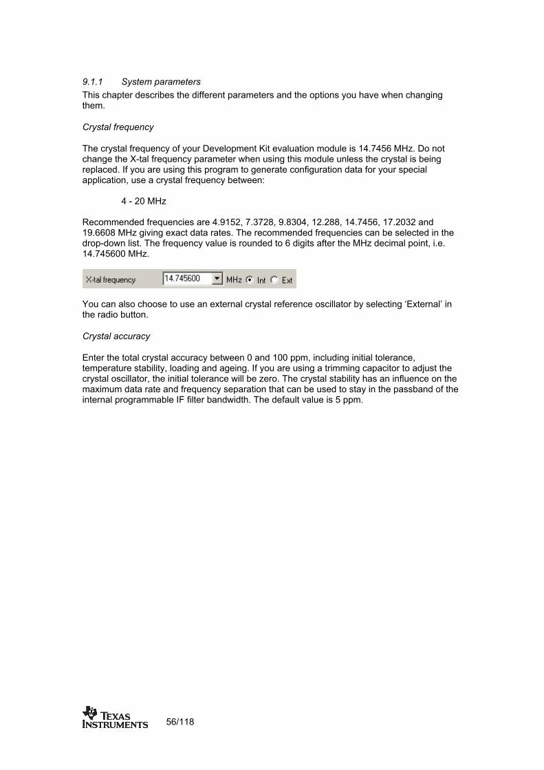
Crystal frequency
The crystal frequency of your Development Kit evaluation module is 14.7456 MHz. Do not change the X-tal frequency parameter when using this module unless the crystal is being replaced. If you are using this program to generate configuration data for your special application, use a crystal frequency between: 4 - 20 MHz Recommended frequencies are 4.9152, 7.3728, 9.8304, 12.288, 14.7456, 17.2032 and 19.6608 MHz giving exact data rates. The recommended frequencies can be selected in the drop-down list. The frequency value is rounded to 6 digits after the MHz decimal point, i.e. 14.745600 MHz.
You can also choose to use an external crystal reference oscillator by selecting ‘External’ in the radio button.
internal programmable IF filter bandwidth. The default value is 5 ppm.
Crystal accuracy
Enter the total crystal accuracy between 0 and 100 ppm, including initial tolerance, temperature stability, loading and ageing. If you are using a trimming capacitor to adjust the crystal oscillator, the initial tolerance will be zero. The crystal stability has an influence on the maximum data rate and frequency separation that can be used to stay in the passband of the
56/118
RF frequency
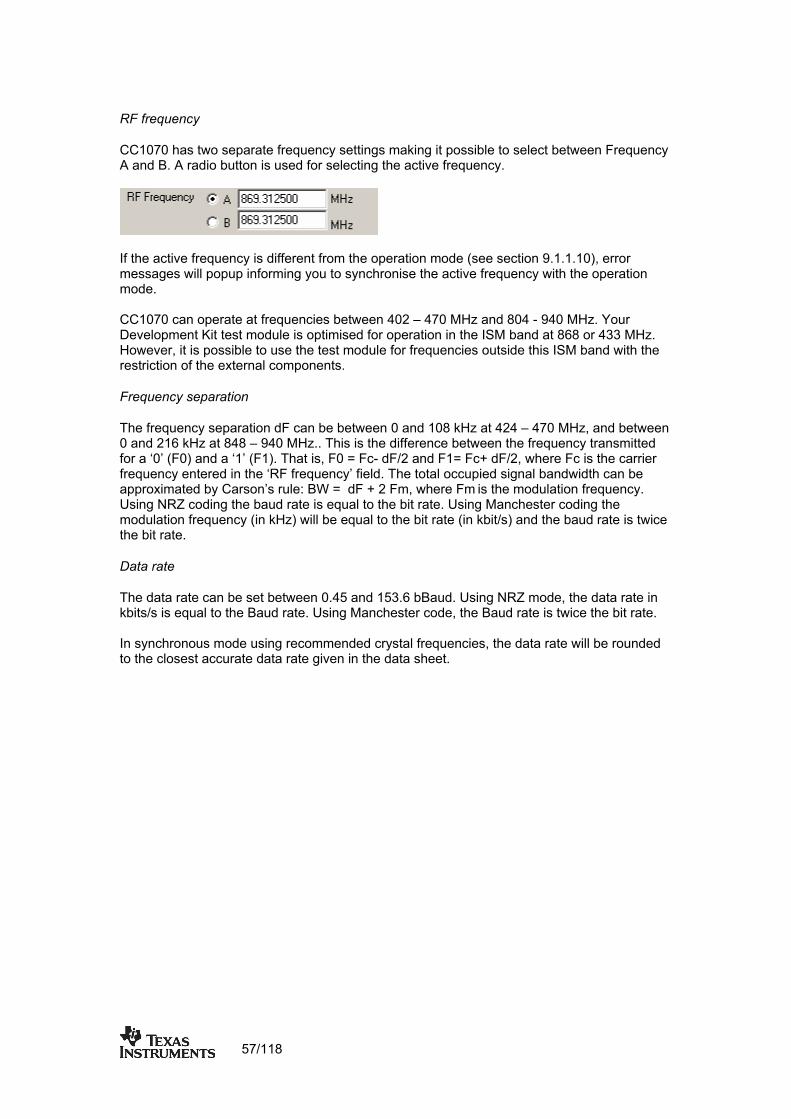
CC1070 has two separate frequency settings making it possible to select between Frequency A and B. A radio button is used for selecting the active frequency.
If the active frequency is different from the operation mode (see section 9.1.1.10), error messages will popup informing you to synchronise the active frequency with the operation mode. CC1070 can operate at frequencies between 402 – 470 MHz and 804 - 940 MHz. Your Development Kit test module is optimised for operation in the ISM band at 868 or 433 MHz. However, it is possible to use the test module for frequencies outside this ISM band with the restriction of the external components.
Frequency separation
The frequency separation dF can be between 0 and 108 kHz at 424 – 470 MHz, and between 0 and 216 kHz at 848 – 940 MHz.. This is the difference between the frequency transmitted for a ‘0’ (F0) and a ‘1’ (F1). That is, F0 = Fc- dF/2 and F1= Fc+ dF/2, where Fc is the carrier frequency entered in the ‘RF frequency’ field. The total occupied signal bandwidth can be approximated by Carson’s rule: BW = dF + 2 Fm, where Fm is the modulation frequency. Using NRZ coding the baud rate is equal to the bit rate. Using Manchester coding the modulation frequency (in kHz) will be equal to the bit rate (in kbit/s) and the baud rate is twice the bit rate.
Data rate
The data rate can be set between 0.45 and 153.6 bBaud. Using NRZ mode, the data rate in kbits/s is equal to the Baud rate. Using Manchester code, the Baud rate is twice the bit rate. In synchronous mode using recommended crystal frequencies, the data rate will be rounded to the closest accurate data rate given in the data sheet.
57/118
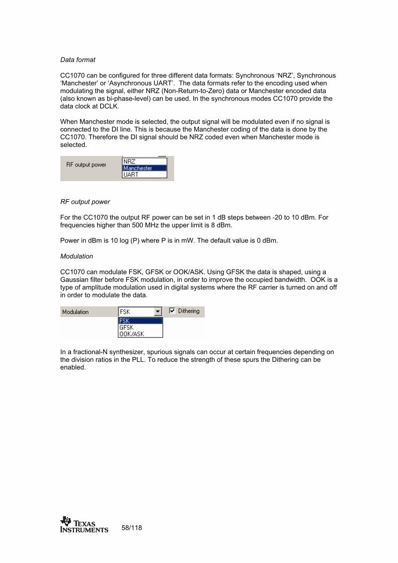
Data format
CC1070 can be configured for three different data formats: Synchronous ‘NRZ’, Synchronous ‘Manchester’ or ‘Asynchronous UART’. The data formats refer to the encoding used when modulating the signal, either NRZ (Non-Return-to-Zero) data or Manchester encoded data (also known as bi-phase-level) can be used. In the synchronous modes CC1070 provide the data clock at DCLK. When Manchester mode is selected, the output signal will be modulated even if no signal is connected to the DI line. This is because the Manchester coding of the data is done by the CC1070. Therefore the DI signal should be NRZ coded even when Manchester mode is selected.
RF output power
For the CC1070 the output RF power can be set in 1 dB steps between -20 to 1frequencies higher than 500 MHz the upper limit is 8 dBm.
0 dBm. For
m is 10 log (P) where P is in mW. The default value is 0 dBm.
ulation, in order to improve the occupied bandwidth. OOK is a pe of amplitude modulation used in digital systems where the RF carrier is turned on and off
in order to modulate the data.
Power in dB
Modulation
CC1070 can modulate FSK, GFSK or OOK/ASK. Using GFSK the data is shaped, using a Gaussian filter before FSK modty
In a fractional-N synthesizer, spurious signals can occur at certain frequencies depending on the division ratios in the PLL. To reduce the strength of these spurs the Dithering can be enabled.
58/118
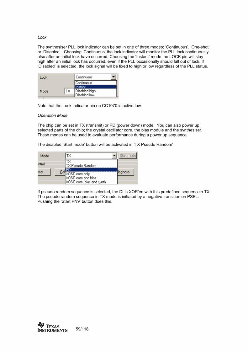
Lock
The synthesiser PLL lock indicator can be set in one of three modes: ‘Continuous’, ‘One-shot’ or ‘Disabled’. Choosing ‘Continuous’ the lock indicator will monitor the PLL lock continuously also after an initial lock have occurred. Choosing the ‘Instant’ mode the LOCK pin will stay high after an initial lock has occurred, even if the PLL occasionally should fall out of lock. If ‘Disabled’ is selected, the lock signal will be fixed to high or low regardless of the PLL status.
so power up elected parts of the chip; the crystal oscillator core, the bias module and the synthesiser.
These modes can be used to evaluate performance during a power up sequence. The disabled ‘Start mode’ button will be activated in ‘TX Pseudo Random’
Note that the Lock indicator pin on CC1070 is active low.
Operation Mode
The chip can be set in TX (transmit) or PD (power down) mode. You can als
If pseudo random sequence is selected, the DI is XOR’ed with this predefined sequencein TX. The pseudo random sequence in TX mode is initiated by a negative transition on PSEL. Pushing the ‘Start PN9’ button does this.
59/118

9.2 The register configuration window for CC1070 When you have chosen the register configuration window, SmartRF® Studio will look like the picture below.
In this mode you can change the Register values by enter the hex values. Please see the data sheet for detailed information on the register settings. The registers are used to program the transceiver chip on the CC1070EM, and the CC1070 will be programmed with the register information when Update device (F5) is pushed. You can also configure each register by pushing the update button for the respective register entry. We dissuade you to change the bits without first study the datasheet or contacting our company. When changing the values and pressing Enter in the Normal configuration window described in chapter 5.1, the frames will change automatically. Changing view to Register View the optimised register values for the Normal View is given.
60/118
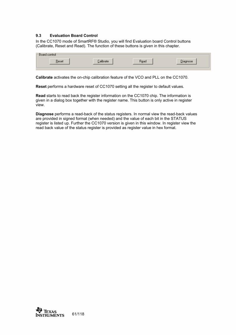
9.3 Evaluation Board Control In the CC1070 mode of SmartRF® Studio, you will find Evaluation board Control buttons (Calibrate, Reset and Read). The function of these buttons is given in this chapter.
Calibrate activates the on-chip calibration feature of the VCO and PLL on the CC1070. Reset performs a hardware reset of CC1070 setting all the register to default values. Read starts to read back the register information on the CC1070 chip. The information is given in a dialog box together with the register name. This button is only active in register view. Diagnose performs a read-back of the status registers. In normal view the read-back values are provided in signed format (when needed) and the value of each bit in the STATUS register is listed up. Further the CC1070 version is given in this window. In register view the read back value of the status register is provided as register value in hex format.
61/118
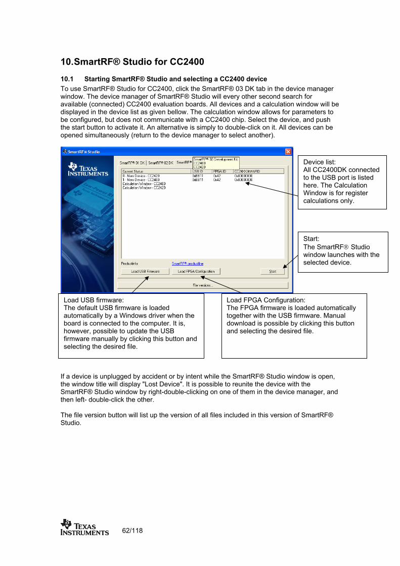
10. SmartRF® Studio for CC2400
10.1 Starting SmartRF® Studio and selecting a CC2400 device To use SmartRF® Studio for CC2400, click the SmartRF® 03 DK tab in the device manager window. The device manager of SmartRF® Studio will every other second search for available (connected) CC2400 evaluation boards. All devices and a calculation window will be displayed in the device list as given bellow. The calculation window allows for parameters to be configured, but does not communicate with a CC2400 chip. Select the device, and push the start button to activate it. An alternative is simply to double-click on it. All devices can be opened simultaneously (return to the device manager to select another).
Device list: All CC2400DK connected to the USB port is listed here. The Calculation Window is for register calculations only.
If a device is unplugged by accident or by intent while the SmartRF® Studio window is open, the window title will display "Lost Device". It is possible to reunite the device with the SmartRF® Studio window by right-double-clicking on one of them in the device manager, and then left- double-click the other. The file version button will list up the version of all files included in this version of SmartRF® Studio.
Start: The SmartRF® Studio window launches with the selected device.
Load FPGA Configuration: The FPGA firmware is loaded automatically together with the USB firmware. Manual download is possible by clicking this button and selecting the desired file.
Load USB firmware: The default USB firmware is loaded automatically by a Windows driver when the board is connected to the computer. It is, however, possible to update the USB firmware manually by clicking this button and selecting the desired file.
62/118
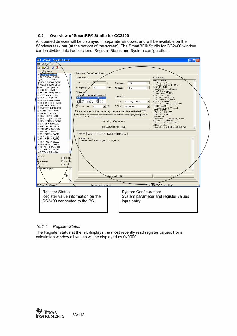
10.2 Overview of SmartRF® Studio for CC2400 All opened devices will be displayed in separate windows, and will be available on the Windows task bar (at the bottom of the screen). The SmartRF® Studio for CC2400 window can be divided into two sections: Register Status and System configuration.
System Configuration:
System parameter and register values input entry.
Register Status: Register value information on the CC2400 connected to the PC.
10.2.1 Register Status The Register status at the left displays the most recently read register values. For a calculation window all values will be displayed as 0x0000.
63/118
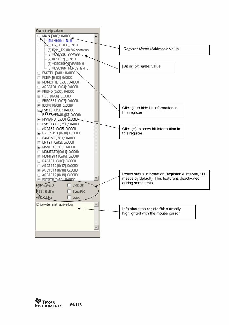
Register Name (Address): Value
[Bit nr] bit name: value
Info about the register/bit currehighlighted with the mouse cursor
Click (+) to show bit informationthis register
in
Click (-) to hide bit information in this register
ntly
Polled status information (adjus 00 msecs by default). This featureduring some tests.
table interval, 1 is deactivated
64/118
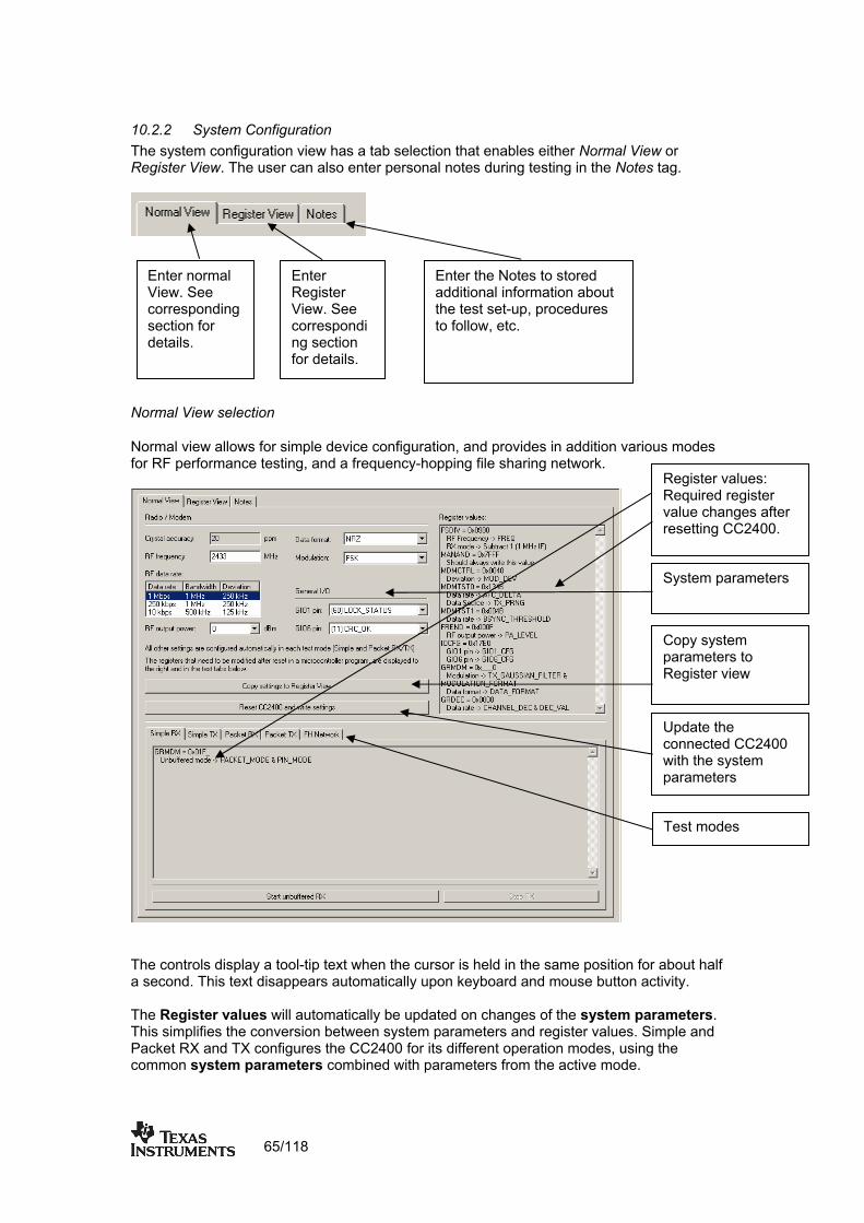
10.2.2 System Configuration The system configuration view has a tab selection that enables either Normal View or Register View. The user can also enter personal notes during testing in the Notes tag.
Normal View selection
Normal view allows for simple device configuration, and provides in addition various modes for RF performance testing, and a frequency-hopping file sharing network.
The controls display a tool-tip text when the cursor is held in the same position for about half a second. This text disappears automatically upon keyboard and mouse button activity. The Register values will automatically be updated on changes of the system parameters. This simplifies the conversion between system parameters and register values. Simple and Packet RX and TX configures the CC2400 for its different operation modes, using the common system parameters combined with parameters from the active mode.
Enter normal View. See corresponding section for details.
Enter Register
section
View. See correspondingfor details.
Enter the Notes to stored additional information about the test set-up, procedures to follow, etc.
Register values: Required register value changes after resetting CC2400.
System parameters
Update the connected CC2400 with the system parameters
Copy system parameters to Register view
Test modes
65/118

The available modes are:
Simple RX/TX:
acket RX/TX:
Configures CC2400 for constant RX/TX mode. These modes are suitable for measuring RF parameters. PConfigures CC2400 for buffered RX/TX operation. Random hexadecimal strings or text can be transferred from one chip to another. CRC errors and lost packets are reported for the receiver. All received packets can be dumped to file if so desired. FH Network: The frequency hopping network allows for up to eight CC2400DK nodes to simultaneously transfer one file to another node in the network. More help on this and the other features is available through tool-tips.
66/118
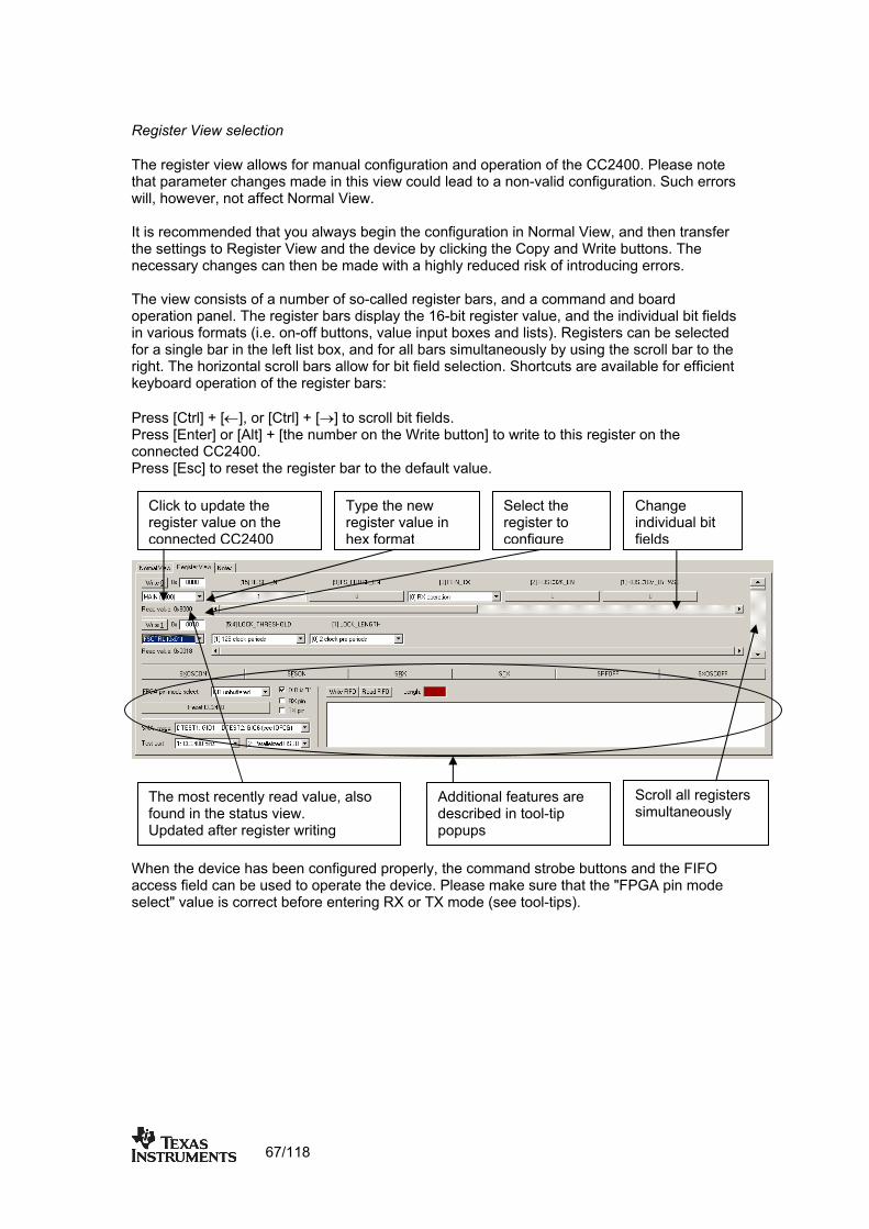
Register View selection
The register view allows for manual configuration and operation of the CC2400. Please note at parameter changes made in this view could lead to a non-valid configth uration. Such errors
will, however, not affect Normal View.
It is recommended that you always begin the configuration in Normal View, and then transfer ettings to Register View and the device by clicking the Copy and Write buttons. The
ry changes can then be made with a highly reduced risk of introducing errors.
mmand and board nel. The register bars display the 16-bit register value, and the individual bit fields
in various formats (i.e. on-off buttons, value input boxes and lists). Registers can be selected for a single bar in the left list box, and for all bars simultaneously by using the scroll bar to the right. The horizontal scroll bars allow for bit field selection. Shortcuts are available for efficient keyboard operation of the register bars: Press [Ctrl] + [←], or [Ctrl] + [→] to scroll bit fields. Press [Enter] or [Alt] + [the number on the Write button] to write to this register on the connected CC2400. Press [Esc] to reset the register bar to the default value.
the snecessa
he view consists of a number of so-called register bars, and a coToperation pa
Select the register to configure
Change individual bit fields
Click to update the register value on the connected CC2400
When the device has been configured properly, the command strobe buttons and the FIFO
e g RX or TX mode (see tool-tips).
access field can be used to operate the device. Please make sure that the "FPGA pin modselect" value is correct before enterin
Type the new register value in hex format
Scroll all registers simultaneously
Additional features are described in tool-tip
The most recently read value, also found in the status view. Updated after register writing popups
67/118

10.2.3 Pull-down menus and toolbar SmartRF® Studio simplifies access to the rest of its features through the use of pull-down menus and a tool bar. The SmartRF® Studio menus are shown below.
File
The File menu allows for settings to be imported and exported.
Reset configuration- This command will reset all fields in SmartRF® Studio. The connected device is not affected. The command is also available from the toolbar (white sheet). Open configuration- This command will open the configuration file *.srfs2400 including Normal View, Register view and Notes settings. The command is also available from the toolbar (open folder). Save configuration - This command saves the Normal View, Register view and Notes settings in a *.srfs2400 configuration file. The command is also available form the toolbar (floppy disk). Load CC2400 state - This command will load register values from a *.stat2400 file into CC2400. Save CC2400 state - This command will save all register values in CC2400 to a *.stat2400 file. Export CC2400 registers - This command will save all CC2400 register values entered in Register View to a standard text file. Import CC2400 registers - This command will copy all CC2400 register values listed in a preformatted external text file into the associated register fields in CC22400 Register View. Export CC2400 code - This command will copy all applicable registers into a C compatible software structure. The structure format is based on corresponding templates which can be changed/added by the user. The code export feature is supported by an associated intuitive
68/118

windows pup-up dialog. The register values changed in register view must be written to the re they will be taken into account by the export function.
he refresh button on the toolbar reads all registers. The values are displayed in the status view to the left and the bars in Register view.
chip befo
Close - Exit the SmartRF® Studio window for this device. You can also use the top-right X-button. T
69/118
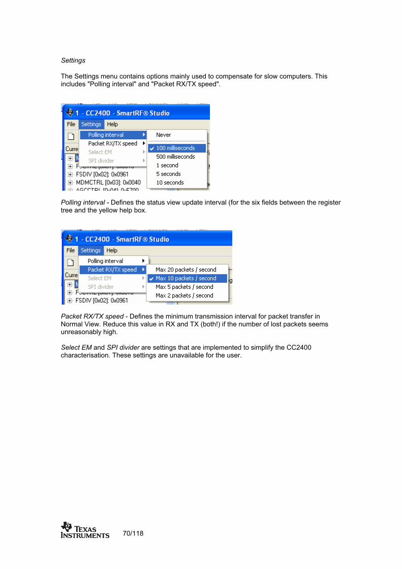
Settings
r slow computers. This cludes "Polling interval" and "Packet RX/TX speed".
The Settings menu contains options mainly used to compensate foin
Polling interval - Defines the status view update interval (for the six fields tree and the yellow help box.
between the register
Packet RX/TX speed - Defines the minimum transmission interval for packet transfer in Normal View. Reduce this value in RX and TX (both!) if the number of lost packets seems
simplify the CC2400 haracterisation. These settings are unavailable for the user.
unreasonably high.
elect EM and SPI divider are settings that are implemented to Sc
70/118

Help
Conta information and disclaimer is available in the help menu.
ct
10.2.4 Online help SmartRF® Studio for CC2400 provides online help through so-called tool-tips. By moving the ursor over a field (e.g. a button or a text field) and holding it in the same position alf a second, the text will appear in a yellow box slightly below the cursor.
c for about h
Tool-tiptransferNetwork mode
on how to files in the FH
aller than 32 bitVi Er ol(s) rsi in Norm
Warnings are indicated by turning the relevant control(s) yellow. One such warning will ap a sync word smpear when choosing
ew.
rors are indicated by turning the relevant contrze larger than 252 in the Packet RX/TX tests
s in the Packet RX/TX tests in Normal
ed. Try for instance to enter a packet al View.
71/118
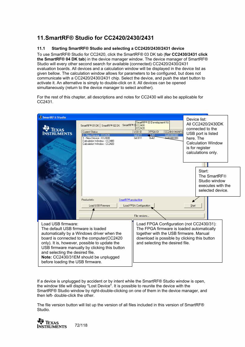
11. SmartRF® Studio for CC2420/2430/2431
11.1 Starting SmartRF® Studio and selecting a CC2420/2430/2431 device o use SmartRF® Studio for CC2420, click the SmartRF® 03 DK tab (for CC2430/24T
th31 click
e SmartRF® 04 DK tab) in the device manager window. The device manager of SmartRF® Studio will every other second search for available (connected) CC2420/2430/2431 evaluation boards. All devices and a calculation window will be displayed in the device list as given bellow. The calculation window allows for parameters to be configured, but does not communicate with a CC2420/2430/2431 chip. Select the device, and push the start button to activate it. An alternative is simply to double-click on it. All devices can be opened simultaneously (return to the device manager to select another). For the rest of this chapter, all descriptions and notes for CC2430 will also be applicable for CC2431.
Device list: All CC2420/2430DK connected to the USB port is listed here. The Calculation Window is for register calculations only.
If a device is unplugged by accident or by intent wh open, the window title will display "Lost Device". It is possSmartRF® Studio window by right-double-clicking on one of them in the device manager, and then left- double-click the other. The file version button will list up the version of all f n of SmartRF® Studio.
ile the SmartRF® Studio window isible to reunite the device with the
iles included in this versio
Start: The SmartRF® Studio window executes with the sele ed device. ct
Load USB firmware: The default USB firmware i loaded automatically by a Windows driver when the board is connected to the computer(CC2420
le to update the
ading the USB firmware.
Load FPGA Configuration (not CC2430/31): The FPGA firmware is loaded automatically together with the USB firmware. Manual download is possible by clicking this button and selecting the desired file.
s
only). It is, however, possibUSB firmware manually by clicking this button and selecting the desired file. Note: CC2430/31EM should be unplugged before lo
72/118

Note that some of the view captures in this section might differ between CC2420 and pose any ambiguity to the understanding and operation of CC2430. However, this should not
SmartRF® Studio for CC2420/2430.
73/118
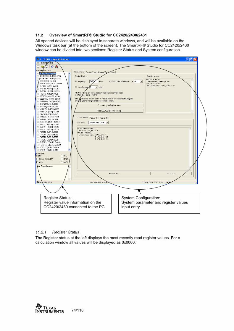
11.2 Overview of SmartRF® Studio for CC2420/2430/2431
bar (at the bottom of the screen). The SmartRF® Studio for CC2420/2430 two sections: Register Status and System configuration.
All opened devices will be displayed in separate windows, and will be available on the Windows taskwindow can be divided into
1.2.1 Register Status
Register Status: System Configuration: Register value information on the System parameter and register values CC2420/2430 connected to the PC. input entry.
1The Register status at the left displays the most recently read register values. For a calculation window all values will be displayed as 0x0000.
74/118

Register Name (Address): Value
[Bit nr] bit name: value
Info about the register/bit currently highlighted with the mouse cursor
Click (+) to show bit information in this register
Click (-) to hide bit information in this register
Polled status information (adjustable interval, 100 msecs by default). This feature is deactivated during some tests.
75/118
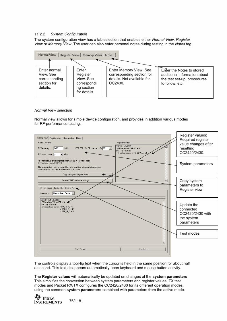
11.2.2 System Configuration The system configuration view has a tab selection that enables either Normal View, Register View or Memory View. The user can also enter personal notes during testing in the Notes tag
.
Normal View selection
Normal view allows for simple device configuration, and provides in addition various modes for RF performance testing.
The controls display a tool-tip text when the cursor is held in the same position for about half a second. This text disappears automatically upon keyboard and mouse button activity. The Register values will automatically be updated on changes of the system parameters. This simplifies the conversion between system parameters and register values. TX test modes and Packet RX/TX configures the CC2420/2430 for its different operation modes, using the common system parameters combined with parameters from the active mode.
Enter normal View. See corresponding section for details.
Enter Register View. See corresponding section for details.
Enter the Notes to sadditional informa
tored tion about
the test set-up, procedures to follow, etc.
Enter Memory View. See corresponding section for details. Not available for CC2430.
Register values: Required register value changes after resetting CC2420/2430.
System parameters
Test modes
Update the connected CC2420/2430 with the system parameters
Copy system parameters to Register view
76/118
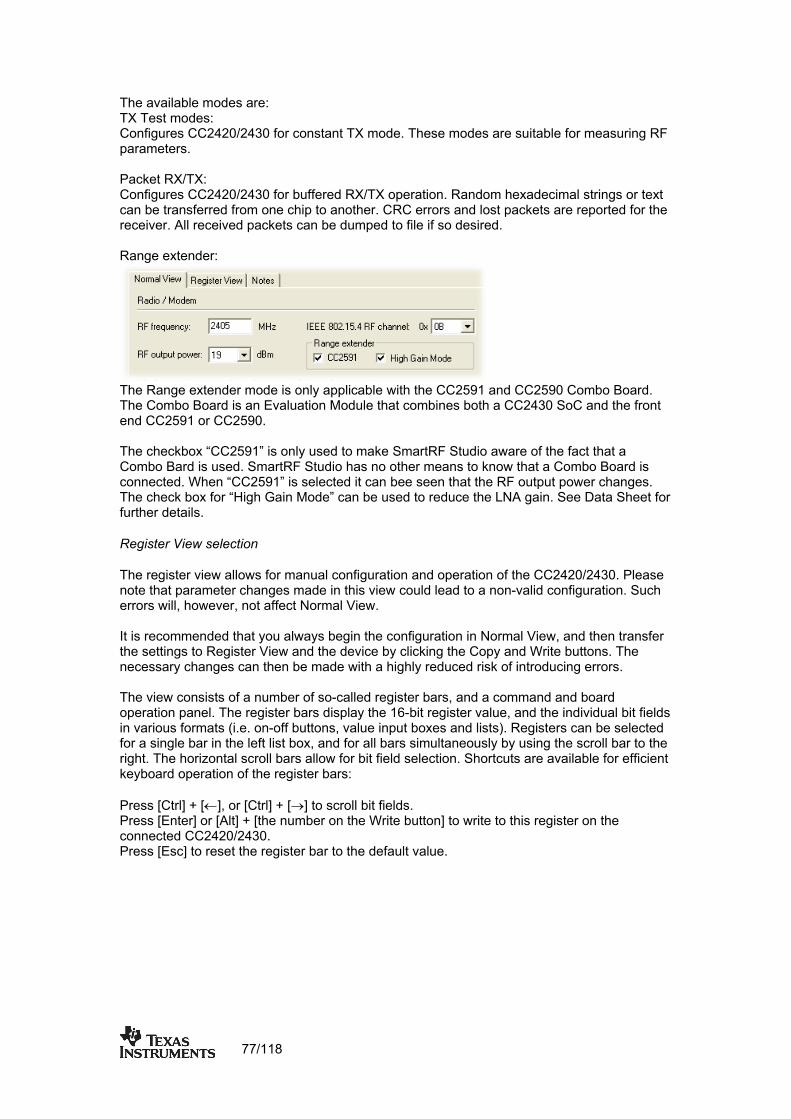
The available modes are: TX Test modes: Configures CC2420/2430 for constant TX mode. These modes are suitable for measuring RF
tion. Random hexadecimal strings or text an be transferred from one chip to another. CRC errors and lost packets are reported for the
ange extender:
parameters. Packet RX/TX: Configures CC2420/2430 for buffered RX/TX operacreceiver. All received packets can be dumped to file if so desired. R
The Range extender mode is only applicable with the CC2591 and CC2590 Combo Board.
Evaluation Module that combines both a CC2430 SoC and the front
591” is only used to make SmartRF Studio aware of the fact that a ed. SmartRF Studio has no other means to know that a Combo Board is
is selected it can bee seen that the RF output power changes. igh Gain Mode” can be used to reduce the LNA gain. See Data Sheet for
r view allows for manual configuration and operation of the CC2420/2430. Please arameter changes made in this view could lead to a non-valid configuration. Such
ot affect Normal View.
is recommended that you always begin the configuration in Normal View, and then transfer ce by clicking the Copy and Write buttons. The
highly reduced risk of introducing errors.
mber of so-called register bars, and a command and board bars display the 16-bit register value, and the individual bit fields
various formats (i.e. on-off buttons, value input boxes and lists). Registers can be selected rs simultaneously by using the scroll bar to the
allow for bit field selection. Shortcuts are available for efficient rs:
] to scroll bit fields. ress [Enter] or [Alt] + [the number on the Write button] to write to this register on the
connected CC2420/2430. Press [Esc] to reset the register bar to the default value.
The Combo Board is an90. end CC2591 or CC25
C2The checkbox “C
Combo Bard is usconnected. When “CC2591”The check box for “Hfurther details.
Register View selection
The registenote that perrors will, however, n Itthe settings to Register View and the devinecessary changes can then be made with a The view consists of a nuoperation panel. The registerinfor a single bar in the left list box, and for all baright. The horizontal scroll barskeyboard operation of the register ba Press [Ctrl] + [←], or [Ctrl] + [→P
77/118

Select the register to configure
78/118
Wh the device has been configured properly, the command strobe can be used to operate
evice. en
the d
Click to update the lue on the
d CC2420/2430
Type the new ister value in
at
Change individual bit fields
register va regconnecte hex form
Scroll all registers ly simultaneous
The most recently read value, also found in the status view. Updated after register writing
Additional features are
popups described in tool-tip
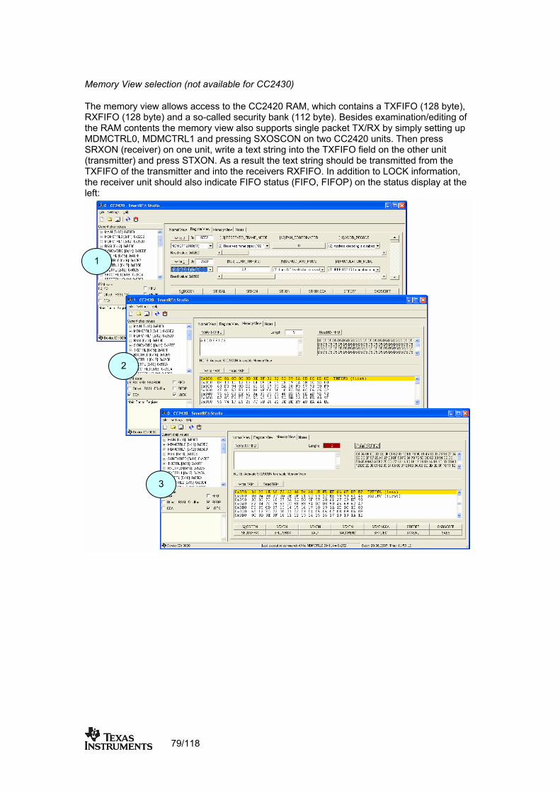
Memory View selection (not available for CC2430)
The memory view allows access to the CC2420 RAM, which contains a TXFIFO (128 byte),
N on two CC2420 units. Then press XON (
(transmitt ress STXON. As a result the text string should be transmitted from the FIFO of the transmitter and into the receivers RXFIFO. In addition to LOCK information,
the receiver unit should also indicate FIFO status (FIFO, FIFOP) on the status display at the left:
RXFIFO (128 byte) and a so-called security bank (112 byte). Besides examination/editing of the RAM contents the memory view also supports single packet TX/RX by simply setting up MDMCTRL0, MDMCTRL1 and pressing SXOSCOSR receiver) on one unit, write a text string into the TXFIFO field on the other unit
er) and pTX
1
2
3
79/118
Transmitting IEEE 802.15.4 compliant packets This section describes how to send a simple IEEE 802.15.4 compliant packet.
First of all, the IEEE 802.15.4 standard is now available for download through this program:
http://standards.ieee.org/getieee802/802.15.html. Please note that the terms and conditions according to this web site apply
g/getieee802/terms.html(http://standards.ieee.or ). you have not downloaded the IEEE 802.15.4 standard yet it is recommended that you do so
now.
An IEEE 802.15.4 packet is built in the following way:
equence number 1 byte] [Address field 0-20 bytes] [Payload XX bytes] [Frame check sequence 2 bytes (FCS)] The frame control field is built in the following way: [bit 0-2 frame type] [bit 3 security enabled] [bit 4 frame pending] [bit 5 ACK request] [bit 6 intra pan] [bit 7-9 reserved] [bit 10-11 dest addr mode] [bit 12-13 reserved] [bit 14-15 src addr mode] There are 4 different frame types:
con
s are not present
If
[Frame control 2 bytes (FCF)] [S
000 Bea001 Data 010 ACK
11 MAC command 0100-111 Reserved There are 3 different addressing modes:
0 PanID and address field001 Reserved 10 16-bit short address 11 64-bit extended address The address field is built in the following way: [Destination PanID 0/2 bytes] [Destination address 0/2/8 bytes] [Source PanID 0/2 bytes] [Source address 0/2/8 bytes]
80/118
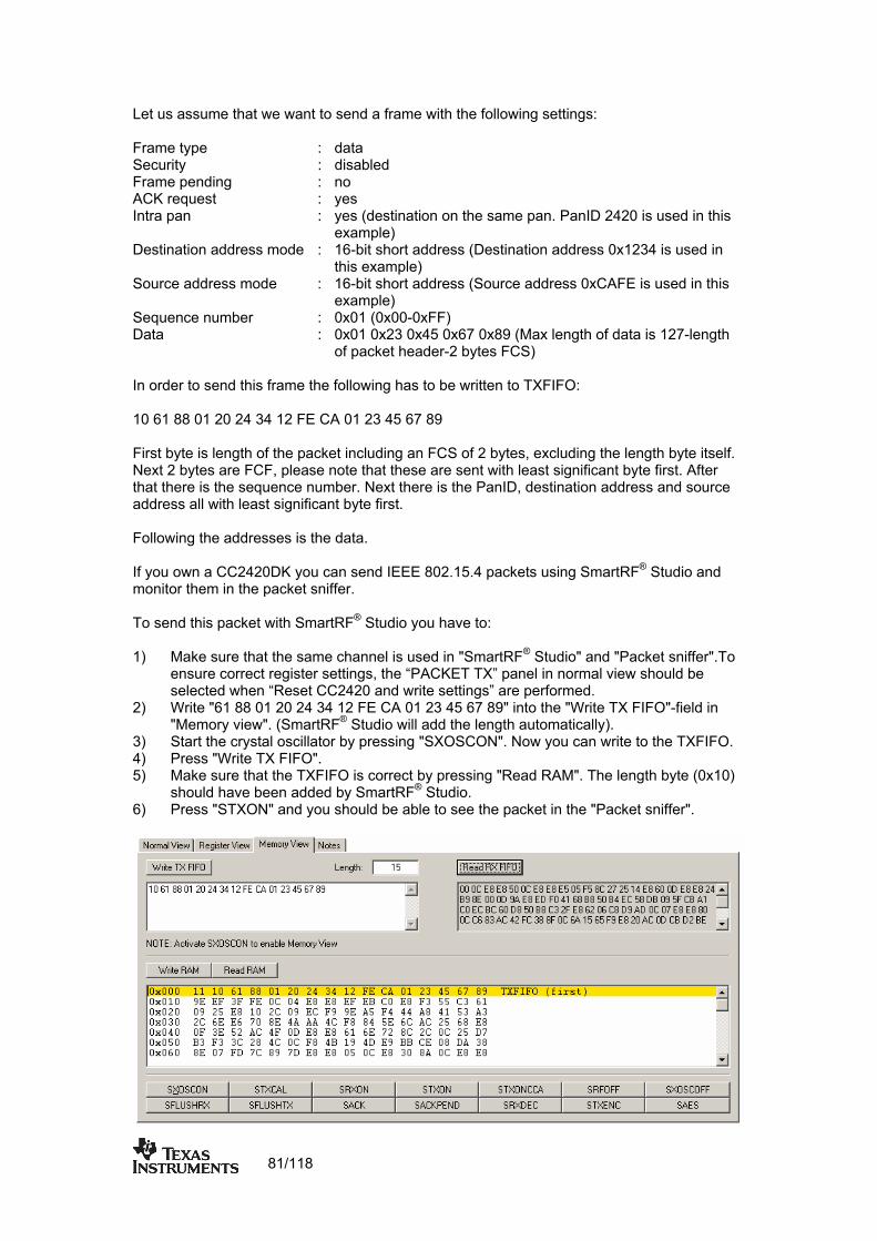
Let us assume that we want to send a frame with the following settings:
pe : data ecurity : disabled
Intra pan : yes (destination on the same pan. PanID 2420 is used in this example)
Destination address mode : 16-bit short address (Destination address 0x1234 is used in this example)
Source address mode : 16-bit short address (Source address 0xCAFE is used in this example)
Sequence number : 0x01 (0x00-0xFF) Data : 0x01 0x23 0x45 0x67 0x89 (Max length of data is 127-length
of packet header-2 bytes FCS) In order to send this frame the following has to be written to TXFIFO: 10 61 88 01 20 24 34 12 FE CA 01 23 45 67 89 First byte is length of the packet including an FCS of 2 bytes, excluding the length byte itself. Next 2 bytes are FCF, please note that these are sent with least significant byte first. After that there is the sequence number. Next there is the PanID, destination address and source address all with least significant byte first. Following the addresses is the data. If you own a CC2420DK you can send IEEE 802.15.4 packets using SmartRF® Studio and monitor them in the packet sniffer. To send this packet with SmartRF® Studio you have to: 1) Make sure that the same channel is used in "SmartRF® Studio" and "Packet sniffer".To
ensure correct register settings, the “PACKET TX” panel in normal view should be selected when “Reset CC2420 and write settings” are performed.
2) Write "61 88 01 20 24 34 12 FE CA 01 23 45 67 89" into the "Write TX FIFO"-field in "Memory view". (SmartRF® Studio will add the length automatically).
3) Start the crystal oscillator by pressing "SXOSCON". Now you can write to the TXFIFO. 4) Press "Write TX FIFO". 5) Make sure that the TXFIFO is correct by pressing "Read RAM". The length byte (0x10)
should have been added by SmartRF® Studio. 6) Press "STXON" and you should be able to see the packet in the "Packet sniffer".
Frame tySFrame pending : no ACK request : yes
81/118
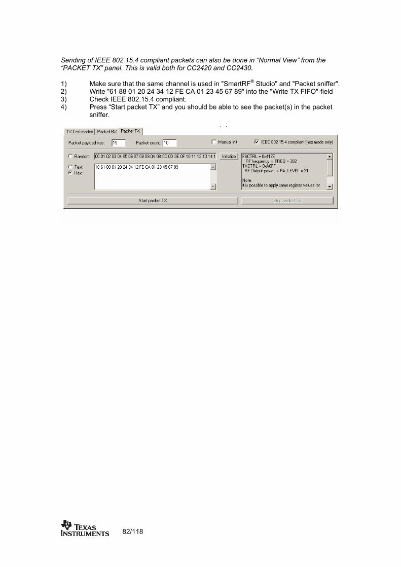
Sending of IEEE 802.15.4 compliant packets can also be done in “Normal View” from the “PACKET TX” panel. This is valid both for CC2420 and CC2430.
SmartRF Studio" and "Packet sniffer". ) Write "61 88 01 20 24 34 12 FE CA 01 23 45 67 89" into the "Write TX FIFO"-field ) Check IEEE 802.15.4 compliant.
4 Press “Start packet TX” and you should be able to see the packet(s) in the packet sniffer.
1) Make sure that the same channel is used in " ®
23
)
82/118
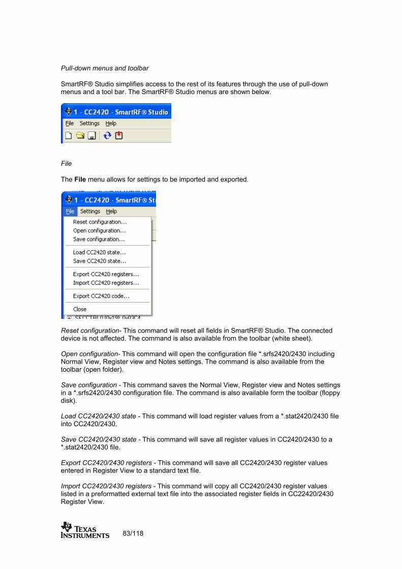
Pull-down menus and toolbar
martRF® Studio simplifies access to the rest of its features through the use of pull-down menus and a tool bar. The SmartRF® Studio menus are shown below. S
File
The File menu allows for settings to be imported and exported.
Reset configuration- This command will reset all fields in SmartRF® Studio. The connected evice is not affected. The command is also available from the toolbar (white sheet).
e
Save configuration - This command saves the Normal View, Register view and Notes settings in a *.srfs2420/2430 configuration file. The command is also available form the toolbar (floppy disk). Load CC2420/2430 state - This command will load register values from a *.stat2420/2430 file into CC2420/2430. Save CC2420/2430 state - This command will save all register values in CC2420/2430 to a *.stat2420/2430 file. Export CC2420/2430 registers - This command will save all CC2420/2430 register values entered in Register View to a standard text file. Import CC2420/2430 registers - This command will copy all CC2420/2430 register values listed in a preformatted external text file into the associated register fields in CC22420/2430 Register View.
d Open configuration- This command will open the configuration file *.srfs2420/2430 including Normal View, Register view and Notes settings. The command is also available from thtoolbar (open folder).
83/118

Export CC2420/2430 code - This command will copy all applicable registers into a C ding templates
re is supported by an ia egister view must
compatible software structure. The structure format is based on corresponwhich can be changed/added by the user. The code export featuassoc ted intuitive windows pup-up dialog. The register values changed in rbe written to the chip before they will be taken into account by the export function. Close - Exit the SmartRF® Studio window for this device. You can also use the top-right X-button. The refresh button on the toolbar reads all registers. The values are displayed in the status view to the left and the bars in Register view.
84/118
Settin gs
The Settings menu contains options mainly used to compensate for slow computers. Thisincludes "Polling interval" and "Packet RX/TX speed".
Polling interval - Defines the status view update interval (for the six fields between the register tree and the yellow help box.
Packet RX/TX speed - Defines the minimum transmission interval for packet transfer in Normal View. Reduce this value in RX and TX (both!) if the number of lost packets seems unreasonably high.
elect EM and SPI divider are settings that are implemented to simplify the CC2420 har e settings are unavailable for th
Sc acterisation. Thes e user.
85/118
Help
Contact information and disclaimer is available in the help menu.
11.2.3 Online help ® Studio for CC2420/2430 provides online help through so-called tool-tips. By
ton or a text field) and holding it in the same position a yellow box slightly below the cursor.
SmartRFmoving the cursor over a field (e.g. a butfor about half a second, the text will appear in
Tool-tip for Packet TX
Warnings are indicated by turning the relevant control(s) yellow. One such warning wiappear when choosing a non - IEEE 802.15.4 frequency channel in Normal View. As aonly TX Test mode will work in Normal View. Errors are indicated by turning the relevant control(s) red. Try for instance to enter a nIEEE 802.15.4 frequency channel (e.g.: 2407 MHz) in Normal View and select Packet RX/TX. As a result the status window for Packet RX/TX will turn red to inform the user that the selected frequency does not support IEEE 802.15.4.
ll result
on -
86/118

12. SmartRF® Studio for CC11xx and 25xx
12.1 Starting SmartRF® Studio and selecting a CC111x/251x device o use SmartRF® Studio fT or CC111x/251x, click the SmartRF® 04 DK tab in the device
. The device manager of SmartRF® Studio will every other second search
e-evice manager to select
en
on
manager windowfor available (connected) SmartRF® 04 evaluation boards. All associated devices and a calculation window will be displayed in the device list as given bellow. The calculation window allows for parameters to be configured, but does not communicate with a CC111x/251x chip.
elect the device, and push the start button to launch it. An alternative is simply to doublSclick on it. All devices can be opened simultaneously (return to the danother). Note: The CC2511/1111 USB Dongle must be powered from the SmartRF04EB board. For detailed description of how to connect the USB Dongle to SmartRF04EB, see “CC2511 USBDongle User Manual”. The ”CC2511/1111 – new device” will be shown in the device list whcorrectly connected. Because of a known problem, the CC2511 device must be switch off/one extra time before start execution of device. .
If a device is unplugged by accident or by intent while the SmartRF® Studio window is open, the window title will display "Lost Device". It is possible to reunite the device with the SmartRF® Studio window by right-double-clicking on one of them in the device manager, and then left- double-click the other. The file version button will list up the version of all files included in this version of SmartRF® Studio.
Load USB firmware: The USB firmware can be update manually by clicking this button and selecting the desired file (normally srf04eb_fwid0400.hex). Note: CCxx10EM should be unplugged before loading the USB firmware.
Start: The SmartRF® Studio window executes with the selected device.
Device list: All SmartRF®connected toport is liste
04 DK the USB
d here. The Calculation Window is for register calculations only.
Load MCU prototype firmware: Loads predefined DK MCU firmware via USB. Inactivates the interface between the DK MCU and SmartRF chip. Allows external MCU full control over the SmartRF chip via a dedicated EB pinrow.
87/118

Note that some of the view captures in this section might differ between CC11xx and CC25xx. However, this should not pose any ambiguity to the understanding and operation of SmartRF® Studio for CC11xx/25xx.
88/118

12.2 Overview of SmartRF® Studio for CC11xx/25xx All opened devices will be displayed in separate windows, and will be available on the Windows task bar (at the bottom of the screen). The SmartRF® Studio for CC11xx/25xx window can be divided into two sections: Register Status and System configuration. Important note: All RX related features described in the following CC11xx/25xx sections does not apply to
0/2550. CC115
12.2.1 Register Status The Register status at the left displays the most recently read register values. For a calculation window all values will be displayed as 0x00.
System Configuration: System parameter and register values input entry. Note that RX related features are not present in CC1150/2550.
Register Status: Register value information on the CC11xx/25xx connected to the PC.
89/118

Register Name (Address): Value
[Bit nr] bit name: value
Click (+) to show bit information in this register
Click (-) to hide bit information in this register
90/118
Info about the register/bit currently highlighted with the mouse cursor
Polled status information (adjustable interval, 100 msecs ng interval will be too
slow in order to catch all the intermediate MARCSTATEs chip.
This feature is deactivated during some tests.
register value et value. See
data sheet for further details. CRC reads the value from PKTSTATUS.CRC_OK RSSI calculated from the RSSI register taking into account the RSSI offset value. See data sheet for further details. OBW: Occupied Bandwidth Lock will be set when the radio enter TX/RX state and the PLL is in lock.
by default). In some cases the polli
of the
Frequency offset is calculated out of theFREQEST. It gives the estimated Freq. offs
12 uration h w ha ction that en r Normal egister View. The user can also enter personal notes during testing in the Notes tag.
.2.2 System Confige system configuration vieT s a tab sele ables eithe View or
R
Normal View selection
Normal view allows for simple device configuration, and provides in addition various modes r RF performance testing, and a frequency-hopping file sharing network.
Enter Register View. See corresponding section for details.
Enter the Notes to stored additional information about the test set-up, procedures to follow, etc.
fo
Enter normal View. See corresponding section for details.
Register values: Required register value changes after resetting CC11xx/25xx
System parameters
Test modes
Update the connected CC11xx/25xx with the system parameters
Copy system parameters to Register view
91/118

The controls display a tool-tip text when the cursor is held in the same position for about half second. This text disappears automatically upon keyboard and mouse button activity.
. r values. Simple and
odes, using the ommon system parameters combined with parameters from the active mode.
a The Register values will automatically be updated on changes of the system parametersThis simplifies the conversion between system parameters and registePacket RX and TX configures the CC11xx/25xx for its different operation mc
92/118
The available modes are: Simple RX/TX: Configures CC11xx/25xx for constant RX/TX mode. These modes are suitable for measuring RF parameters. Packet RX/TX: Configures CC11xx/25xx for buffered RX/TX operation. Random hexadecimal strings or text can be transferred from one chip to another. CRC errors and lost packets are reported for the receiver. All received packets can be dumped to file if so desired. PER test (only available for CC1100/CC1101/2500): This is the same feature as the stand-alone SmartRF®04EB PER test, described in the SmartRF®04DK User Manual. However, instead of using the SmartRF®04EB joystick to browse a SmartRF®04EB LCD menu, all associated parameters are remote set/configured from SmartRF® Studio at the PC. SmartRF®04EB Preset 3 (stored in the SmartRF®04EB FLASH) will be overwritten by the new selected SmartRF® Studio settings, so even if the SmartRF®04EB is disconnected from SmartRF® Studio, it is still possible to run the SmartRF®04 PER test in stand-alone mode with other settings than the ones pre-defined in the SmartRF®04EB-firmware. As with the stand-alone SmartRF®04EB PER-tester, the slave unit should be started before the master unit. Note that the PER test should be started at least one time from SmartRF® Studio in order to get Preset 3 settings on SmartRF04EB. Only the settings of the master unit will be stored in preset 3. When the PER test is started, the settings of the master unit will be transferred to the slave unit (over the air). It doesn’t matter what ever settings has been defined for the slave unit in SmartRF Studio.
93/118
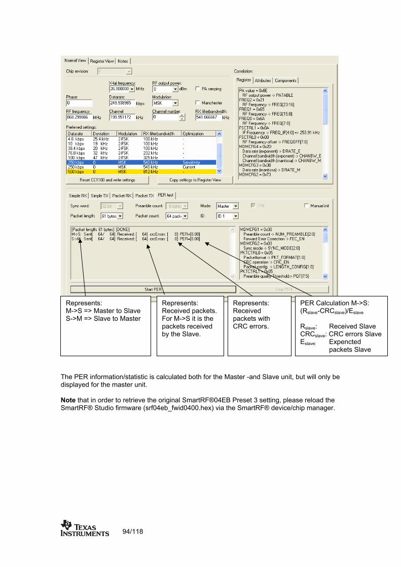
The PER information/statistic is calculated both for the Master -and Slave unit, but will only be
ote that in order to retrieve the original SmartRF®04EB Preset 3 setting, please reload the er.
displayed for the master unit. NSmartRF® Studio firmware (srf04eb_fwid0400.hex) via the SmartRF® device/chip manag
Represents: M->S => Master to Slave S->M => Slave to Master
Represents: Received packets. For M->S it is the
packets received by the Slave.
Represents: Received
PER Calculat(R -CR
ion M->S: slave Cslave)/Eslave
ived Slave errors Slave
slave: packets Slave
packets with Rslave: ReceCRCslave: CRCE Expencted
CRC errors.
94/118
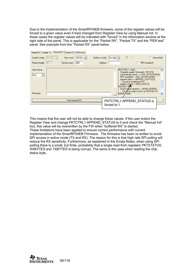
Due to the implementation of the SmartRF04EB firmware, some of the register values will be
rced to a given value even if tried changed from Register View by using Manual Init. In
e “Packet RX”, “Packet TX” and the “PER test” panel. See example from the “Packet RX” panel below.
fothese cases the register values will be indicated with “forced” in the information window at theright side of the panel. This is applicable for th
This means that the user will not be able to change these values. If the user enters the Register View and change PKTCTRL1.APPEND_STATUS to 0 and check the “Manual Init” box, this value will be overwritten by the FW when “buffered RX” is started. These limitations have been applied to ensure correct performance with current implementation of the SmartRF04EB Firmware. The firmware has been re-written to avoid SPI access in active mode (TX and RX). The reason for this is that high rate SPI polling will reduce the RX sensitivity. Furthermore, as explained in the Errata Notes, when using SPI polling there is a small, but finite, probability that a single read from registers PKTSTATUS, RXBYTES and TXBYTES is being corrupt. The same is the case when reading the chip status byte.
PKTCTRL1.APPEND_STATUS is forced to 1.
95/118
Register View selection ter view allows for manual configuration and operation of the CC11xx/25xx. Please
note that parameter changes made in this view could lead to a non-valid configuration. Such
is recommended that you always begin the configuration in Normal View, and then transfer the settings to Register View and the device by clicking the Copy and Write buttons. The
ecessary changes can then be made with a highly reduced risk of introducing errors.
of so-called register bars, and a command and board peration panel. The register bars display the 8-bit register value, and the individual bit fields various formats (i.e. on-off buttons, value input boxes and lists). Registers can be selected
for a single bar in the left list box, and for all bars simultaneously by using the scroll bar to the right. The horizontal scroll bars allow for bit field selection. Shortcuts are available for efficient keyboard operation of the register bars: Press [Ctrl] + [←], or [Ctrl] + [→] to scroll bit fields. Press [Enter] or [Alt] + [the number on the Write button] to write to this register on the connected CC11xx/25xx. Press [Esc] to reset the register bar to the default value.
if
packet length is used. Also that CRC check is enabled and that the tatus bytes are appended to the RX FIFO.
The regis
errors will, however, not affect Normal View. It
n The view consists of a numberoin
Be aware that the SmartRF®04EB PER tester firmware will overwrite some registers even these are tried changed from Register View. The SmartRF®04EB PER tester requires that
ormal mode and variablens
96/118

Select the register to
e
Change individual bit fields
hen the device has been configured properly, the command strobe buttons and the FIFO + ATABLE access fields can be used to operate the device.
WP
Click to update the register value on the connected CC11xx/25xx configur
Type the new register value in hex format
Additional features are described in tool-tip popups
Scroll all registers simultaneously
The most recently read value, also found in the status view. Updated after register writing
97/118
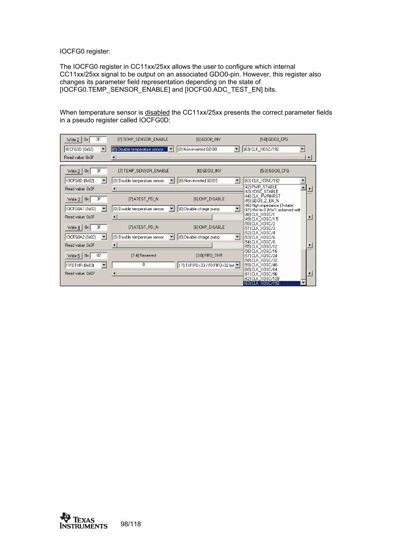
IOCFG0 register:
ser to configure which internal ver, this register also
The IOCFG0 register in CC11xx/25xx allows the uCC11xx/25xx signal to be output on an associated GDO0-pin. Howechang s its parameter field representation depending on the state oe f [IOCFG0.TEMP_SENSOR_ENABLE] and [IOCFG0.ADC_TEST_EN] bits. When temperature sensor is disabled the CC11xx/25xx presents the correct parameter fields in a pseudo register called IOCFG0D:
98/118
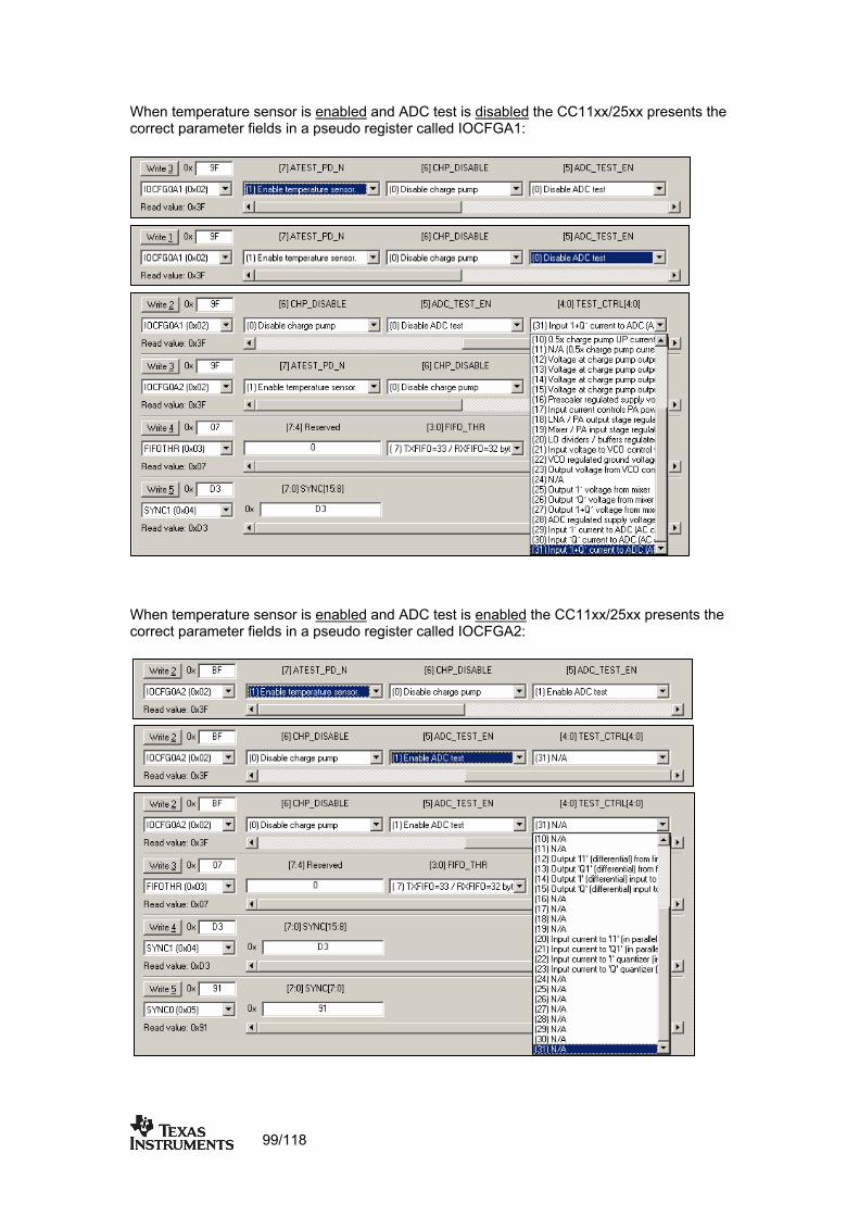
When temperature sensor is enabled and ADC test is disabled the CC11xx/25xx presents the t FGA1:
When temperature sensor is enabled
correc parameter fields in a pseudo register called IOC
and ADC test is enabled the CC11xx/25xx presents the correct parameter fields in a pseudo register called IOCFGA2:
99/118
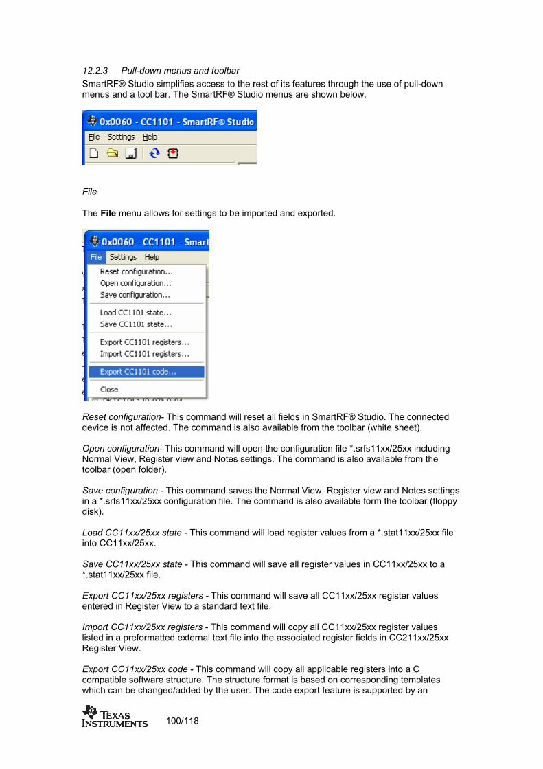
12.2.3 Pull-down menus and toolbar ccess to the rest of its features through the use of pull-down SmartRF® Studio simplifies a
menus and a tool bar. The SmartRF® Studio menus are shown below.
File
The File menu allows for settings to be imported and exported.
Reset configuration- This command will reset all fields in SmartRF® Studio. The connected device is not affected. The command is also available from the toolbar (white sheet). Open configuration- This command will open the confNormal View, Register view and Notes settings. Thtoolbar (open folder). Save configuration - This command saves the Normin a *.srfs11xx/25xx configuration file. The commandisk). Load CC11xx/25xx state - This command will load x file into CC11xx/25xx. Save CC11xx/25xx state - This command will save all register values in CC11xx/25xx to a *.stat11xx/25xx file. Export CC11xx/25xx registers - This command will save all CC11xx/25xx register values entered in Register View to a standard text file. Import CC11xx/25xx registers - This command will copy all CC11xx/25xx register values listed in a preformatted external text file into the associated register fields in CC211xx/25xx Register View. Export CC11xx/25xx code - This command will copy all applicable registers into a C compatible software structure. The structure format is based on corresponding templates which can be changed/added by the user. The code export feature is supported by an
register values from a *.stat11xx/25x
iguration file *.srfs11xx/25xx including e command is also available from the
al View, Register view and Notes settings d is also available form the toolbar (floppy
100/118

associated intuitive windows pup-up dialog. The register values changed in register view must re they will be taken into account by the export function.
refresh button on the toolbar reads all registers. The values are displayed in the status view to the left and the bars in Register view.
be written to the chip befo Close - Exit the SmartRF® Studio window for this device. You can also use the top-right X-button. The
101/118
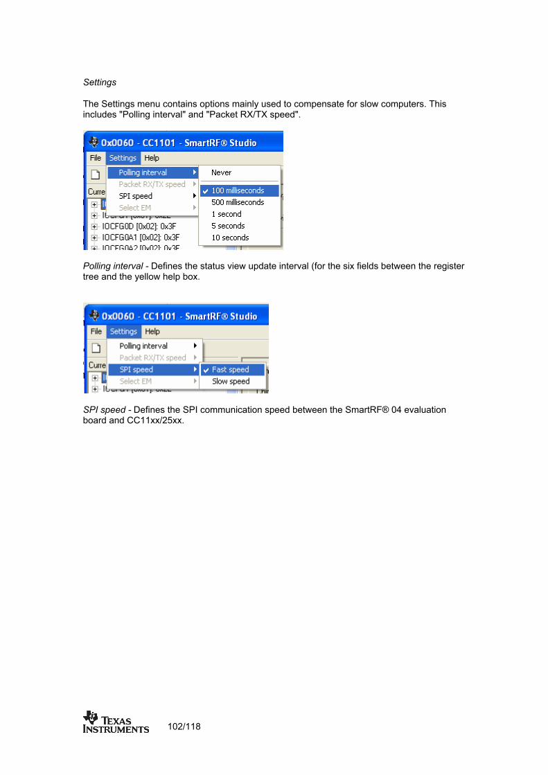
Settings
The Settings menu contains options mainly used to compensate for slow computers. This includes "Polling interval" and "Packet RX/TX speed".
Polling interval - Defines the status view update interval (for the six fields between the registertree and the yellow help box.
SPI speed - Defines the SPI communication speed between the SmartRF® 04 evaluation board and CC11xx/25xx.
102/118
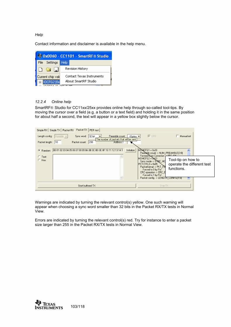
He
o disclaim le in the help
lp
ntact information andC er is availab menu.
12.2.4 Online help martRF® Studio for CC11xx/25xx provides online help through so-called tool-tips. By oving the cursor over a field (e.g. a button or a text field) and holding it in the same position r about half a second, the text will appear in a yellow box slightly below the cursor.
Smfo
Tool-tip on how to operate the different test functions.
Warnings are indicated by turning the relevant control(s) yellow. One such warning will appear when chV
oosing a sync word smaller than 32 bits in the Packet RX/TX tests in Normal iew.
rrors are indicated by turning the relevant control(s) red. Try for instance to enter a packet size the Packet RX/TX tests in Normal View.
E larger than 255 in
103/118
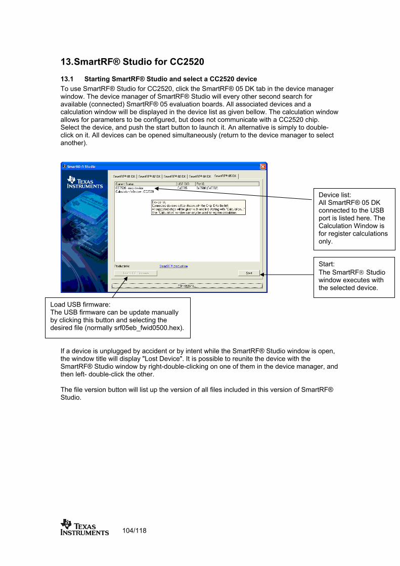
13
13.1 Starting SmartRF® Studio and select a CC2520 device To use SmartRF® Studio for CC2520, click the SmartRF® 05 DK tab in the device manager window. The device manager of SmartRF® Studio will every other second search for ava All associated devices and a calc s given bellow. The calculation window allows for parameters to be configured, but does not communicate with a CC2520 chip. Select the device, and push the start button to launch it. An alternative is simply to double-clicano
. SmartRF® Studio for CC2520
ilable (connected) SmartRF® 05 evaluation boards.ulation window will be displayed in the device list a
k on it. All devices can be opened simultaneously (return to the device manager to select ther).
If a device is unplugged by accident or by intent while the SmartRF® Studio window is opthe window title will display "Lost Device". It is possible to reunite the device with the
martRF® Studio wi
en,
ndow by right-double-clicking on one of them in the device manager, and Sthen left- double-click the other. The file version button will list up the version of all files included in this version of SmartRF®
tudio. S
Device list: All SmartRF® 05 DK connected to the USB port is listed here. The Calculation Window is for register calculations only.
Start: The SmartRF® Studio window executes with the selected device.
LoaThe USB firm nually by des
d USB firmware: ware can be update ma
clicking this button and selecting the ired file (normally srf05eb_fwid0500.hex).
104/118
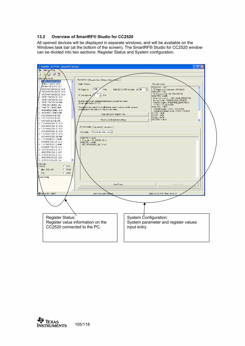
13.2 Overview of SmartRF® Studio for CC2520 ows, and will be available on the
® Studio for CC2520 window System configuration.
All opened devices will be displayed in separate windWindows task bar (at the bottom of the screen). The SmartRFcan be divided into two sections: Register Status and
System Configuration: System parameter and register values input entry.
Register StatRegister value information on the CC2520 connected to the PC.
us:
105/118
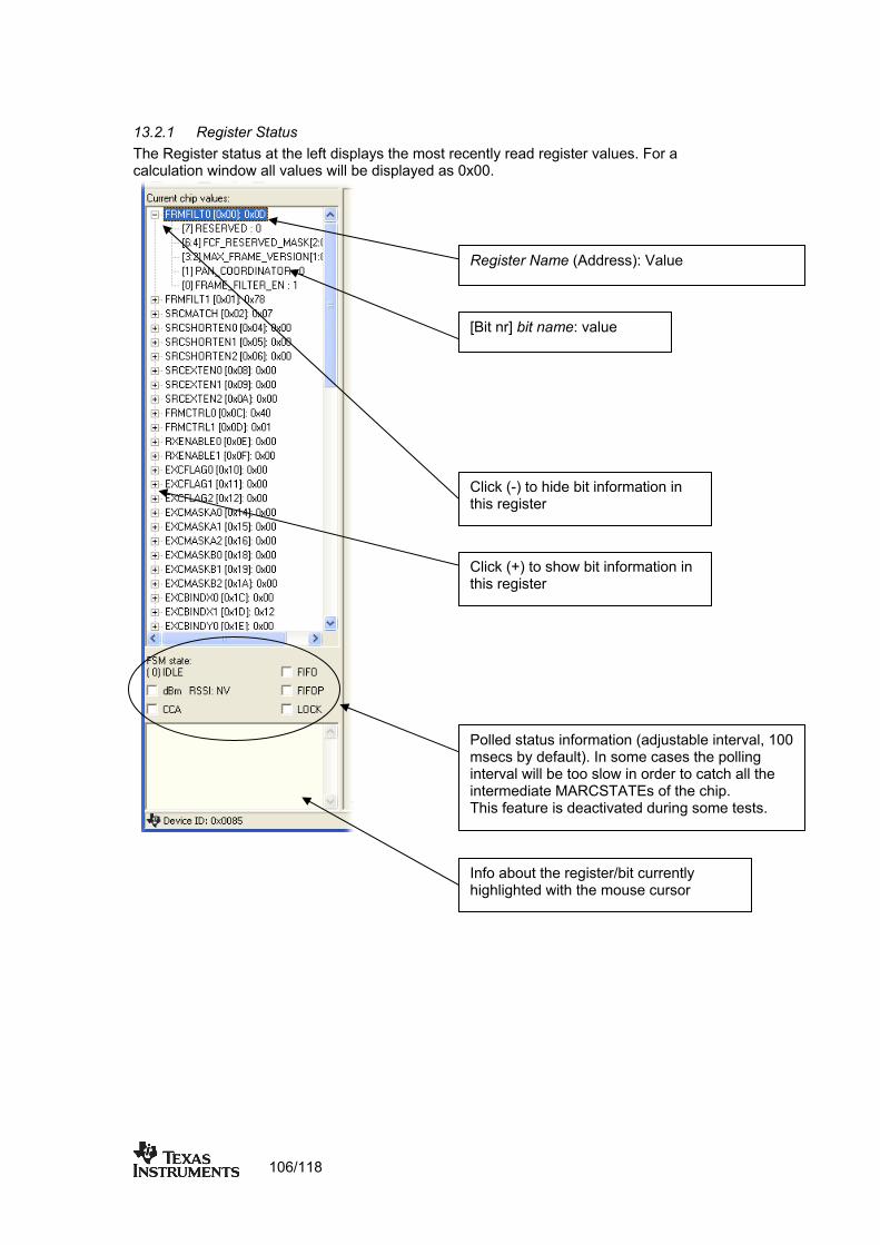
13.2.1 Register Status gi e most recently read register values. For a The Re ster status at the left displays th
calculation window all values will be displayed as 0x00.
Register Name (Address): Value
[Bit nr] bit name: value
Click (+) to show bit information in
Click (-) to hide bit information in this register
this register
Info about the register/bit currently
highlighted with the mouse cursor
Polled status information (adjustable interval, 100 msecs by default). In some cases thinterval will be too slow in order to cat
e polling ch all the
intermediate MARCSTATEs of the chip. This feature is deactivated during some tests.
106/118
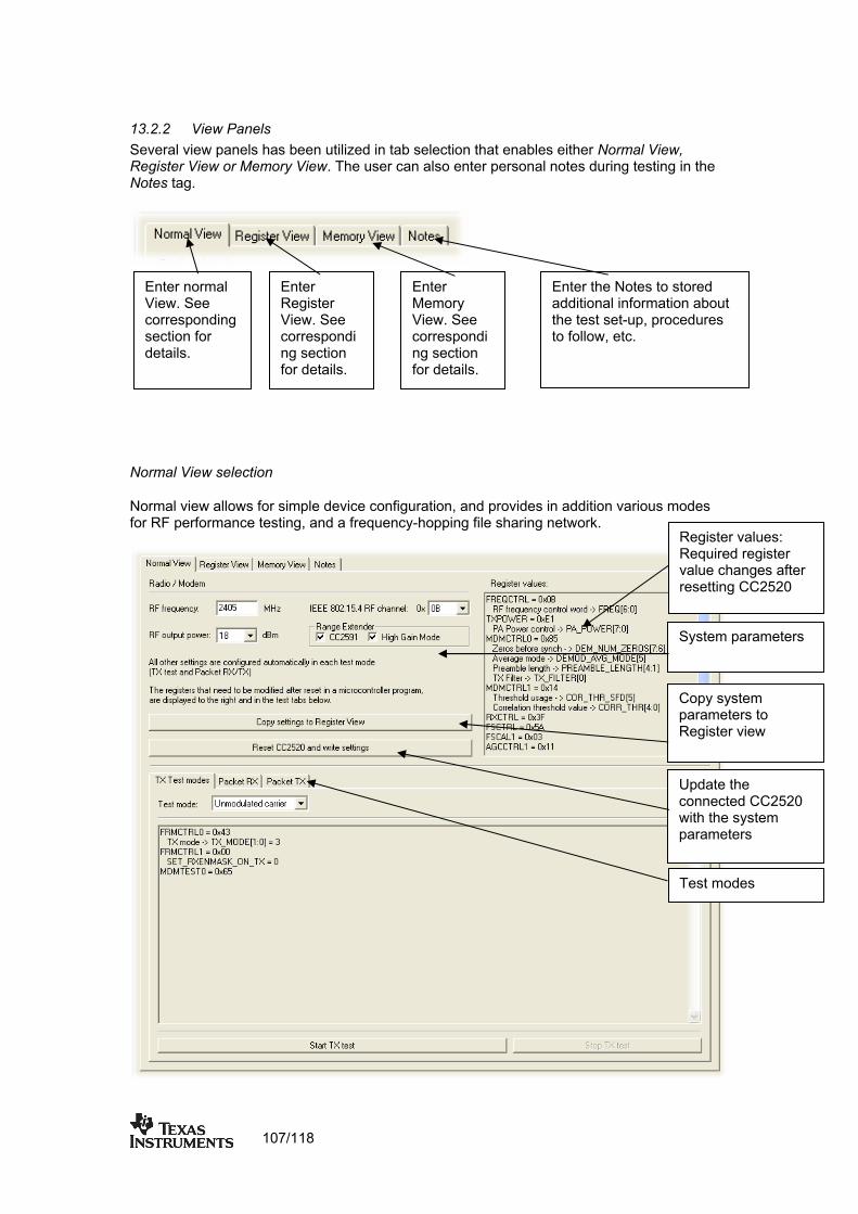
13.2.2 View Panels Several view panels has been utilized in tab selection that enables either Normal View, Register View or Memory View. The user can also enter personal notes during testing in the Notes tag.
Normal View selection
Normal view allows for simple device configuration, and provides in addition various modes for RF performance testing, and a frequency-hopping file sharing network.
Enter normal View. See corresponding section for details.
Enter Register View. See corresponding section for details.
Enter the Notes to stored additional information about the test set-up, procedures to follow, etc.
Register values: Required register value changes after resetting CC2520
System parameters
Update the connected CC2520 with the system parameters
Copy system parameters to Register view
Test modes
Enter Memory View. See corresponding section for details.
107/118

ols display a tool-tip text when the cursor is held in the same position for about half
a second. This text disappears automatically upon keyboard and mouse button activity.
changes of the system parameters. his simplifies the conversion between system parameters and register values. TX Test
modes and Packet RX and TX configure the CC2520 for its different operation modes, using e common system parameters combined with parameters from the active mode.
X Test modes: Configures CC2520 for constant TX mode. These modes are suitable for measuring RF parameters. Packet RX/TX: Configures CC2520 for buffered RX/TX operation. Random hexadecimal strings or text can be transferred from one chip to another. CRC errors and lost packets are reported for the receiver. All received packets can be dumped to file if so desired.
The contr
The Register values will automatically be updated on T
th The available modes are: T
Range extender:
The Range extender mode is only applicable with the CC2591 and CC2590 Combo Board. The Combo Board is an Evaluation Module that combines both a CC2520 and the front end CC2591 or CC2590. The checkbox “CC2591” is only used to make SmartRF Studio aware of the fact that a Combo Bard is used. SmartRF Studio has no other means to know that a Combo Board is connected. When “CC2591” is selected it can bee seen that the RF output power changes. The check box for “High Gain Mode” can be used to reduce the LNA gain. See Data Sheet for further details.
Register View selection
The register view allows for manual configuration and operation of the CC2520. Please note that parameter changes made in this view could lead to a non-valid configuration. Such errors will, however, not affect Normal View. It is recommended that you always begin the configuration in Normal View, and then transfer the settings to Register View and the device by clicking the Copy and Write buttons. The necessary changes can then be made with a highly reduced risk of introducing errors. The view consists of a number of so-called register bars, and a command and board operation panel. The register bars display the 8-bit register value, and the individual bit fields in various formats (i.e. on-off buttons, value input boxes and lists). Registers can be selected for a single bar in the left list box, and for all bars simultaneously by using the scroll bar to the right. The horizontal scroll bars allow for bit field selection. Shortcuts are available for efficient keyboard operation of the register bars: Press [Ctrl] + [←], or [Ctrl] + [→] to scroll bit fields. Press [Enter] or [Alt] + [the number on the Write button] to write to this register on the connected CC2520.
108/118

Press [Esc] to reset the register bar to the default value.
109/118
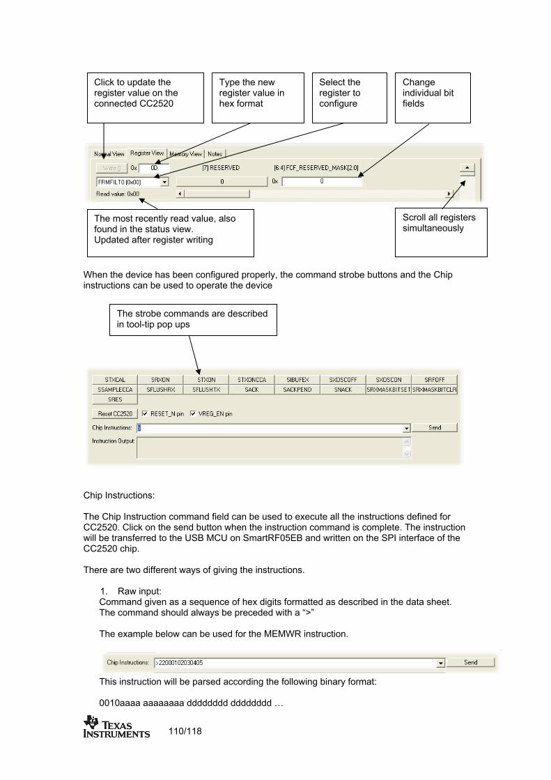
110/118
When the device has been configured properly, the command strobe buttons and the Chip instructions can be used to operate the device
Chip Instructions: The Chip Instruction command field can be used to execute all the instructions defined for CC2520. Click on the send button when the instruction command is complete. The instruction will be transferred to the USB MCU on SmartRF05EB and written on the SPI interface of the CC2520 chip. There are two different ways of giving the instructions.
1. Raw input: Command given as a sequence of hex digits formatted as described in the data sheet. The command should always be preceded with a “>” The example below can be used for the MEMWR instruction.
This instruction will be parsed according the following binary format: 0010aaaa aaaaaaaa dddddddd dddddddd …
Change individual bit fields
Select the register to
Click to update the register value on the connected CC2520 configure
Type the new register value in hex format
Scroll all registers simultaneously
The most recently read value, also found in the status view. Updated after register writing
The strobe commands are described in tool-tip pop ups
ate: by the selected template. Each instruction is given with a template
s the required parameters.
OpCode: 4 bits Address: 12 bits Data: 40 bits In this example the Operation Code is 0x2 and the address is 0x200.
2. Using a templThe syntax is defined that indicate
The template should be replaced with real values:
Most of the templates show all the bytes that should be given and a character is used to indicate the meaning of each nibble in the byte.
The characters should be replaced with real digits. In the example above the template should be replaced with: “REGWR(0x0C, 0x41)”. The following characters are used: a, e, k, n: Address data d: Data p: Priority m: Security c: Count -: Don’t care
For further details about the chip instructions see the Data Sheet.
Memory View selection
The memory view allows access to the CC2520 RAM from address 0x100 to 0x3FF. This includes TXFIFO (128 byte) and RXFIFO (128 byte). There are also two 16-byte temporary areas CBCTEMPH and CBCTEMPL. Besides examination/editing of the RAM contents the memory view also supports single packet TX/RX. The easiest way to do this is to select “Packet RX” in Normal View (Receiver) and press “reset and write” button to write register values to the chip. Go to Memory View and press SXOSCON and SRXON. Nearly the same thing should be done on the transmitter. Select “Packet TX” in Normal View and press “reset and write” button to write register values to the chip. Go to Memory View and press SXOSCON.
111/118
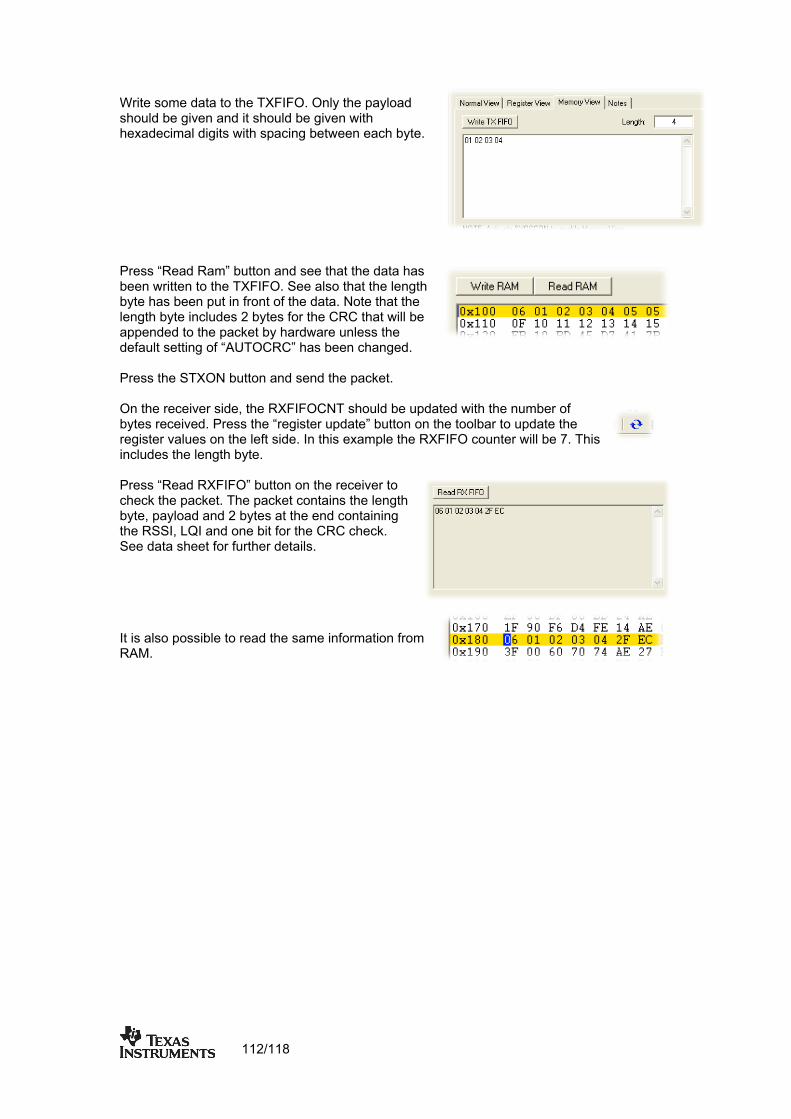
112/118
Write some data to the TXFIFO. Only the payload should be given and it should be given with hexadecimal digits with spacing between each byte. Press “Read Ram” button and see that the data has been written to the TXFIFO. See also that the length byte has been put in front of the data. Note that the length byte includes 2 bytes for the CRC that will be appended to the packet by hardware unless the default setting of “AUTOCRC” has been changed. Press the STXON button and send the packet. On the receiver side, the RXFIFOCNT should be updated with the number of bytes received. Press the “register update” button on the toolbar to update the register values on the left side. In this example the RXFIFO counter will be 7. This includes the length byte. Press “Read RXFIFO” button on the receiver to check the packet. The packet contains the length byte, payload and 2 bytes at the end containing the RSSI, LQI and one bit for the CRC check. See data sheet for further details. It is also possible to read the same information from RAM.
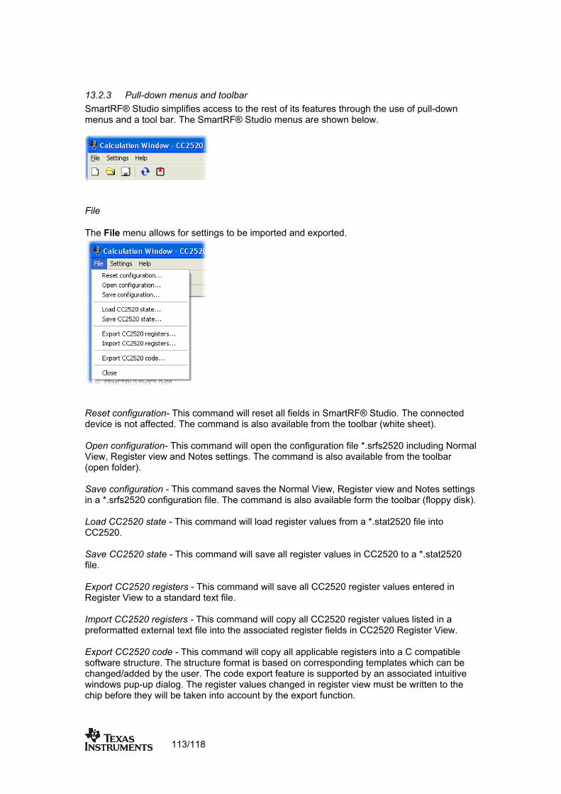
113/118
13.2.3 Pull-down menus and toolbar SmartRF® Studio simplifies access to the rest of its features through the use of pull-down menus and a tool bar. The SmartRF® Studio menus are shown below.
File
The File menu allows for settings to be imported and exported.
Reset configuration- This command will reset all fields in SmartRF® Studio. The connected device is not affected. The command is also available from the toolbar (white sheet). Open configuration- This command will open the configuration file *.srfs2520 including Normal View, Register view and Notes settings. The command is also available from the toolbar (open folder). Save configuration - This command saves the Normal View, Register view and Notes settings in a *.srfs2520 configuration file. The command is also available form the toolbar (floppy disk). Load CC2520 state - This command will load register values from a *.stat2520 file into CC2520. Save CC2520 state - This command will save all register values in CC2520 to a *.stat2520 file. Export CC2520 registers - This command will save all CC2520 register values entered in Register View to a standard text file. Import CC2520 registers - This command will copy all CC2520 register values listed in a preformatted external text file into the associated register fields in CC2520 Register View. Export CC2520 code - This command will copy all applicable registers into a C compatible software structure. The structure format is based on corresponding templates which can be changed/added by the user. The code export feature is supported by an associated intuitive windows pup-up dialog. The register values changed in register view must be written to the chip before they will be taken into account by the export function.

114/118
Close - Exit the SmartRF® Studio window for this device. You can also use the top-right X-button. The refresh button on the toolbar reads all registers. The values are displayed in the status view to the left and the bars in Register view.
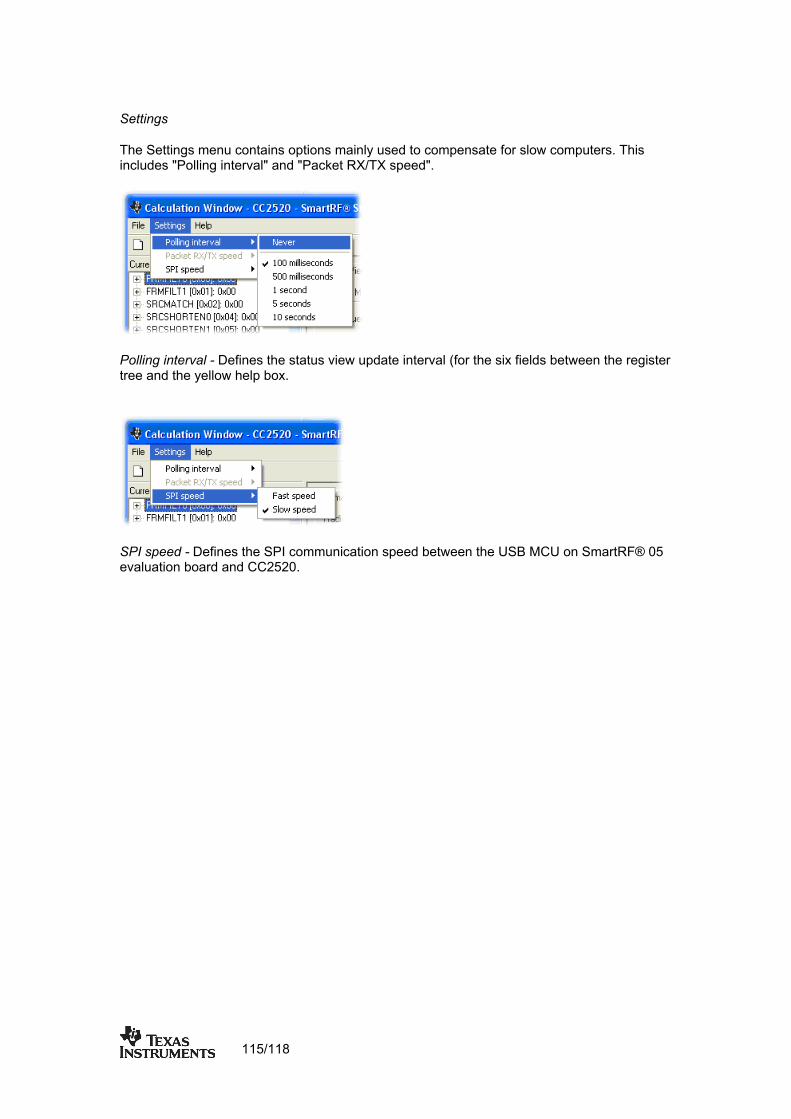
115/118
Settings
The Settings menu contains options mainly used to compensate for slow computers. This includes "Polling interval" and "Packet RX/TX speed".
Polling interval - Defines the status view update interval (for the six fields between the register tree and the yellow help box.
SPI speed - Defines the SPI communication speed between the USB MCU on SmartRF® 05 evaluation board and CC2520.
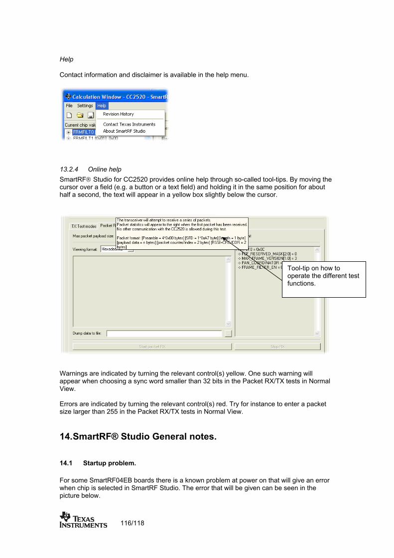
116/118
Help
Contact information and disclaimer is available in the help menu.
13.2.4 Online help SmartRF® Studio for CC2520 provides online help through so-called tool-tips. By moving the cursor over a field (e.g. a button or a text field) and holding it in the same position for about half a second, the text will appear in a yellow box slightly below the cursor.
Warnings are indicated by turning the relevant control(s) yellow. One such warning will appear when choosing a sync word smaller than 32 bits in the Packet RX/TX tests in Normal View. Errors are indicated by turning the relevant control(s) red. Try for instance to enter a packet size larger than 255 in the Packet RX/TX tests in Normal View.
14. SmartRF® Studio General notes.
14.1 Startup problem. For some SmartRF04EB boards there is a known problem at power on that will give an error when chip is selected in SmartRF Studio. The error that will be given can be seen in the picture below.
Tool-tip on how to operate the different test functions.

117/118
The problem is related to the use of the power switch on the SmartRF04EB board. When the switch is turned on, the boot sequence on the USB MCU will sometimes fail. One way to avoid the problem is to leave the power switch on and only plug/unplug the USB plug to set power on/off. If the problem occurs, it can be solved by turning the power switch off and then on again.

118/118
15. Address Information Web sites: HTUhttp://www.ti.com/lpw UTH Technical Support: [email protected]
Worldwide Product Information Centers: HTUContact TI PIC Centers for Technical SuppoUUr UTTUtUTH Headquarters: Texas Instruments Norway AS Gaustadalléen 21 N-0349 Oslo NORWAY Tel: +47 22 95 85 44 Fax: +47 22 95 85 46 T
© 2006, Texas Instruments. All rights reserved.
IMPORTANT NOTICETexas Instruments Incorporated and its subsidiaries (TI) reserve the right to make corrections, modifications, enhancements, improvements,and other changes to its products and services at any time and to discontinue any product or service without notice. Customers shouldobtain the latest relevant information before placing orders and should verify that such information is current and complete. All products aresold subject to TI’s terms and conditions of sale supplied at the time of order acknowledgment.TI warrants performance of its hardware products to the specifications applicable at the time of sale in accordance with TI’s standardwarranty. Testing and other quality control techniques are used to the extent TI deems necessary to support this warranty. Except wheremandated by government requirements, testing of all parameters of each product is not necessarily performed.TI assumes no liability for applications assistance or customer product design. Customers are responsible for their products andapplications using TI components. To minimize the risks associated with customer products and applications, customers should provideadequate design and operating safeguards.TI does not warrant or represent that any license, either express or implied, is granted under any TI patent right, copyright, mask work right,or other TI intellectual property right relating to any combination, machine, or process in which TI products or services are used. Informationpublished by TI regarding third-party products or services does not constitute a license from TI to use such products or services or awarranty or endorsement thereof. Use of such information may require a license from a third party under the patents or other intellectualproperty of the third party, or a license from TI under the patents or other intellectual property of TI.Reproduction of TI information in TI data books or data sheets is permissible only if reproduction is without alteration and is accompaniedby all associated warranties, conditions, limitations, and notices. Reproduction of this information with alteration is an unfair and deceptivebusiness practice. TI is not responsible or liable for such altered documentation. Information of third parties may be subject to additionalrestrictions.Resale of TI products or services with statements different from or beyond the parameters stated by TI for that product or service voids allexpress and any implied warranties for the associated TI product or service and is an unfair and deceptive business practice. TI is notresponsible or liable for any such statements.TI products are not authorized for use in safety-critical applications (such as life support) where a failure of the TI product would reasonablybe expected to cause severe personal injury or death, unless officers of the parties have executed an agreement specifically governingsuch use. Buyers represent that they have all necessary expertise in the safety and regulatory ramifications of their applications, andacknowledge and agree that they are solely responsible for all legal, regulatory and safety-related requirements concerning their productsand any use of TI products in such safety-critical applications, notwithstanding any applications-related information or support that may beprovided by TI. Further, Buyers must fully indemnify TI and its representatives against any damages arising out of the use of TI products insuch safety-critical applications.TI products are neither designed nor intended for use in military/aerospace applications or environments unless the TI products arespecifically designated by TI as military-grade or "enhanced plastic." Only products designated by TI as military-grade meet militaryspecifications. Buyers acknowledge and agree that any such use of TI products which TI has not designated as military-grade is solely atthe Buyer's risk, and that they are solely responsible for compliance with all legal and regulatory requirements in connection with such use.TI products are neither designed nor intended for use in automotive applications or environments unless the specific TI products aredesignated by TI as compliant with ISO/TS 16949 requirements. Buyers acknowledge and agree that, if they use any non-designatedproducts in automotive applications, TI will not be responsible for any failure to meet such requirements.Following are URLs where you can obtain information on other Texas Instruments products and application solutions:Products ApplicationsAmplifiers amplifier.ti.com Audio www.ti.com/audioData Converters dataconverter.ti.com Automotive www.ti.com/automotiveDSP dsp.ti.com Broadband www.ti.com/broadbandClocks and Timers www.ti.com/clocks Digital Control www.ti.com/digitalcontrolInterface interface.ti.com Medical www.ti.com/medicalLogic logic.ti.com Military www.ti.com/militaryPower Mgmt power.ti.com Optical Networking www.ti.com/opticalnetworkMicrocontrollers microcontroller.ti.com Security www.ti.com/securityRFID www.ti-rfid.com Telephony www.ti.com/telephonyRF/IF and ZigBee® Solutions www.ti.com/lprf Video & Imaging www.ti.com/video
Wireless www.ti.com/wireless
Mailing Address: Texas Instruments, Post Office Box 655303, Dallas, Texas 75265Copyright © 2008, Texas Instruments Incorporated