SM-M307F/FN Common
92
SM-M307F/FN Common Mobile Device CONTENTS 1. Safety Precautions 2. Specification 3. Product Function 4. Exploded View and Parts list 5. MAIN Electrical Parts List 6. Level 1 Repair 7. Level 2 Repair 8. Level 3 Repair 9. Reference Abbreviation Notice: All functionality, features, specifications, and other product information provided in this document, including but not limited to, benefits, design, pricing, components, performance, availability, and capabiliti-es of the product are subject to change without notice. Samsung reserves the right to alter this doc-ument or the product described herein at anytime, without obligation to provide notification of such changes.
-
Upload
khangminh22 -
Category
Documents
-
view
5 -
download
0
Transcript of SM-M307F/FN Common

SM-M307F/FN
Common
Mobile Device CONTENTS
1. Safety Precautions
2. Specification
3. Product Function
4. Exploded View and Parts list
5. MAIN Electrical Parts List
6. Level 1 Repair
7. Level 2 Repair
8. Level 3 Repair
9. Reference Abbreviation
4.
2Notice: All functionality, features, specifications,
and other product information provided in this
document, including but not limited to, benefits,
design, pricing, components, performance,
availability, and capabiliti-es of the product are
subject to change without notice. Samsung
reserves the right to alter this doc-ument or the
product described herein at anytime, without
obligation to provide notification of such
changes.

Confidential and proprietary-the contents in this service guide subject to change without prior notice
Distribution, transmission, or infringement of any content or data from this document without Samsung’s written authorization is strictly prohibited.
1. Safety Precautions
1-1. Repair Precaution
Before attempting any repair or detailed tuning, shield the device from RF noise or static electricity discharges.
Use only demagnetized tools that are specifically designed for small electronic repairs, as most electronic parts are sensitive to electromagnetic forces.
Use only high quality screwdrivers when servicing products. Low quality screwdrivers can easily damage the heads of screws.
Use only conductor wire of the properly gauge and insulation for low resistance, because of the low margin of error of most testing equipment. We recommend 22-gauge twisted copper wire.
Hand-soldering is not recommended, because printed circuit boards (PCBs) can be easily damaged, even with relatively low heat. Never use a soldering iron with a power rating of more than 100 watts and use only lead-free solder with a melting point below 250°C (482°F).
Prior to disassembling the battery charger for repair, ensure that the AC power is disconnected.Always use the replacement parts that are registered in the SEC system. Third-party replacement parts may not function properly.

Confidential and proprietary-the contents in this service guide subject to change without prior notice
Distribution, transmission, or infringement of any content or data from this document without Samsung’s written authorization is strictly prohibited.
1. Safety Precautions
1-2. ESD(Electrostatically Sensitive Devices) Precaution
Many semiconductors and ESDs in electronic devices are particularly sensitive to static discharge and can be easily damaged by it. We recommend protecting these components with conductive anti-static bags when you store or transport them.
Always use an anti-static strap or wristband and remove electrostatic buildup or dissipate static electricity from your body before repairing ESDs.
Ensure that soldering irons have AC adapter with ground wires and that the ground wires are properly connected.
Use only desoldering tools with plastic tips to prevent static discharge.
Properly shield the work environment from accidental electrostatic discharge before opening packages containing ESDs.
The potential for static electricity discharge may be increased in low humidity environments, such as air-conditioned rooms. Increase the airflow to the working area to decrease the chance of accidental static electricity discharges.

Confidential and proprietary-the contents in this service guide subject to change without prior notice
Distribution, transmission, or infringement of any content or data from this document without Samsung’s written authorization is strictly prohibited.
2. Specification
2-1. GSM General Specification
Item GSM 850 EGSM 900 DCS1800 PCS1900
Freq. Band[MHz]
Uplink/Downlink
824~849
869~894
880~915
925~960
1710~1785
1805~1880
1850~1910
1930~1990
ARFCN range 128~251 0~124 & 975~1023 512~885 512~810
Tx/Rx spacing 45MHz 45MHz 95MHz 80MHz
Mod. Bit rate/
Bit Period
270.833kbps
3.692us
270.833kbps
3.692us
270.833kbps
3.692us
270.833kbps
3.692us
Time Slot Period/
Frame Period
576.9us
4.615ms
576.9us
4.615ms
576.9us
4.615ms
576.9us
4.615ms
Modulation GSM/
EGPRS
GMSK/
8PSK
GMSK/
8PSK
GMSK/
8PSK
GMSK/
8PSK
MS Power 33dBm~5dBm 33dBm~5dBm 30dBm~0dBm 30dBm~0dBm
Power Class 4(GMSK)
E2(8PSK)
4(GMSK)
E2(8PSK)
1(GMSK)
E2(8PSK)
1(GMSK)
E2(8PSK)
Sensitivity -102dBm -102dBm -100dBm -100dBm
TDMA Mux 8 8 8 8
Confidential and proprietary-the contents in this service guide subject to change without prior notice
Distribution, transmission, or infringement of any content or data from this document without Samsung’s written authorization is strictly prohibited.
2. Specification
2-2. GSM Tx Power Class
TX Power
control level GSM850
TX Power
control level EGSM900
TX Power
control level DCS1800
TX Power
control level PCS1900
5 33±2 dBm 5 33±2 dBm 0 30±3 dBm 0 30±3 dBm
6 31±2 dBm 6 31±2 dBm 1 28±3 dBm 1 28±3 dBm
7 29±2 dBm 7 29±2 dBm 2 26±3 dBm 2 26±3 dBm
8 27±2 dBm 8 27±2 dBm 3 24±3 dBm 3 24±3 dBm
9 25±2 dBm 9 25±2 dBm 4 22±3 dBm 4 22±3 dBm
10 23±2 dBm 10 23±2 dBm 5 20±3 dBm 5 20±3 dBm
11 21±2 dBm 11 21±2 dBm 6 18±3 dBm 6 18±3 dBm
12 19±2 dBm 12 19±2 dBm 7 16±3 dBm 7 16±3 dBm
13 17±2 dBm 13 17±2 dBm 8 14±3 dBm 8 14±3 dBm
14 15±2 dBm 14 15±2 dBm 9 12±4 dBm 9 12±4 dBm
15 13±2 dBm 15 13±2 dBm 10 10±4 dBm 10 10±4 dBm
16 11±3 dBm 16 11±3 dBm 11 8±4 dBm 11 8±4 dBm
17 9±3 dBm 17 9±3 dBm 12 6±4 dBm 12 6±4 dBm
18 7±3 dBm 18 7±3 dBm 13 4±4 dBm 13 4±4 dBm
19 5±3 dBm 19 5±3 dBm 14 2±5 dBm 14 2±5 dBm
- - - - 15 0±5 dBm 15 0±5 dBm

Confidential and proprietary-the contents in this service guide subject to change without prior notice
Distribution, transmission, or infringement of any content or data from this document without Samsung’s written authorization is strictly prohibited.
2. Specification
2-3. WCDMA General Specification
Item WCDMA2100(B1) WCDMA1900(B2) WCDMA850(B5) WCDMA900(B8)
Freq. Band[MHz]
Uplink/Downlink
1920~1980
2110~2170
1850~1910
1930~1990
824~849
869~894
880~915
925~960
ARFCN range
UL:9612~9888
DL:10562~10838
UL:9262~9538
DL:9662~9938
UL:4132~4233
DL:4357~4458
UL:2712~2868
DL:2937~3088
Tx/Rx spacing 190MHz 80MHz 45MHz 45MHz
Mod. Bit rate/
Bit Period
42.2Mbps(DL)
5.42Mbps(UL)
42.2Mbps(DL)
5.42Mbps(UL)
42.2Mbps(DL)
5.42Mbps(UL)
42.2Mbps(DL)
5.42Mbps(UL)
Time Slot Period/
Frame Period
WCDMA
10ms/0.667ms
HSPA
2ms/0.667ms
WCDMA
10ms/0.667ms
HSPA
2ms/0.667ms
WCDMA
10ms/0.667ms
HSPA
2ms/0.667ms
WCDMA
10ms/0.667ms
HSPA
2ms/0.667ms
Modulation
QPSK 16QAM 64QAM
QPSK 16QAM 64QAM
QPSK 16QAM 64QAM
QPSK 16QAM 64QAM
MS Power
(dBm) 25.7 ~ -49(↓) 25.7 ~ -49(↓) 25.7 ~ -49(↓) 25.7 ~ -49(↓)
Power Class 3(max+24dBm) 3(max+24dBm) 3(max+24dBm) 3(max+24dBm)
Sensitivity -106dBm -104dBm -104dBm -103dBm

Confidential and proprietary-the contents in this service guide subject to change without prior notice
Distribution, transmission, or infringement of any content or data from this document without Samsung’s written authorization is strictly prohibited.
2. Specification
2-4. LTE General Specification
Item LTE Band1 LTE Band3 LTE Band5 LTE Band7 LTE Band8
Freq. Band[MHz]
Uplink/Downlink
1920~1980
2110~2170
1710~1785
1805~1880
824~849
869~894
2500~2570
2620~2690
880~915
925~960
ARFCN range UL:18000~18599
DL:0~599
UL:19200~19949
DL:1200~1949
UL:20400~20649
DL:2400~2649
UL:20750~21449
DL:2750~3449
UL:21450-21799
DL:3450-3799
Tx/Rx spacing
(MHz) 190 95 45 120 45
Channel Bandwidth
(MHz) 5/10/15/20 1.4/3/5/10/15/20 1.4/3/5/10 5/10/15/20 1.4/3/5/10
Modulation QPSK,16/64QAM
256QAM(DL only)
QPSK,16/64QAM
256QAM(DL only)
QPSK,16/64QAM
256QAM(DL only)
QPSK,16/64QAM
256QAM(DL only)
QPSK,16/64QAM
256QAM(DL only)
MS Power (dBm) 25.7~-39(↓) 25.7~-39(↓) 25.7~-39(↓) 25.7~-39(↓) 25.7~-39(↓)
Sensitivity (QPSK,
BW 10MHz) (dBm) -96.3 -93.3 -94.3 -94.3 -93.3
Item LTE Band20 LTE Band28 LTE Band38 LTE Band40 LTE Band41
Freq. Band[MHz]
Uplink/Downlink
832~862
791~821
703~748
758~803 2570~2620 2300~2400 2496~2690
ARFCN range UL:24150~24449
DL:6150~6449
UL:27210~27659
DL:9210~9659
UL/DL:37750 ~
38249
UL/DL:38650 ~
39649
UL/DL:39650 ~
41589
Tx/Rx spacing (MHz) -41 55 0 0 0
Channel Bandwidth
(MHz) 5/10/15/20 3/5/10/15/20 5/10/15/20 5/10/15/20 5/10/15/20
Modulation QPSK,16/64QAM
256QAM(DL only)
QPSK,16/64QAM
256QAM(DL only)
QPSK,16/64QAM
256QAM(DL only)
QPSK,16/64QAM
256QAM(DL only)
QPSK,16/64QAM
256QAM(DL only)
MS Power (dBm) 25.7~-39(↓) 25.7~-39(↓) 25.7~-39(↓) 25.7~-39(↓) 25.7~-39(↓)
Sensitivity(QPSK,
BW 10MHz) (dBm) -93.3 -94.8 -96.3 -96.3 -94.3

Confidential and proprietary-the contents in this service guide subject to change without prior notice
Distribution, transmission, or infringement of any content or data from this document without Samsung’s written authorization is strictly prohibited.
3. Product Function
Main Function
Item Description
OS Android P OS V9.0
RF
GSM850 / GSM900 / DCS1800 / PCS1900
WCDMA: B1/ B2/ B5/ B8
LTE: B1/B3/B5/B7/B8/B20/B38/B40/B41
Battery 6000mAh
Base Band 2.3Ghz Quad + 1.7GHz Quad
Other RF GPS, Glonass, Beidou, Galileo / BT5.0 / USB 2.0 / WIFI 802.11 a/b/g/n/ac / NFC(SM-M307FN Only)
Camera Triple Camera ( 48MP(F2.0) + 5MP(F2.2) + 8MP(F2.2)) with LED Flash / Front Camera 16MP(F2.0)
LCD 6.4", FHD+, 2400x1080
RAM 4GB / 6GB
Storage 64GB / 128GB
Sensor Accelerometer, Fingerprint Sensor, Gyro Sensor, Geomagnetic Sensor, Proximity Sensor, Grip
sensor
Accessory Charger: 9V/1.67A and 5V/2.0A AFC charging
Data cable: 3.0pi, 0.8m(USB-C)
Ear phone: 3.5pi, 4pin

Confidential and proprietary-the contents in this service guide subject to change without prior noticeDistribution, transmission, or infringement of any content or data from this document without Samsung’s written authorization is strictly prohibited.
4. Exploded View and Parts List
4-1. Cellular phone Exploded View
QFR01
QAR01
QMO01QME03QCA02
QMP01
QCA01
QCR12
QAN02
QCR205
QKP01
QRE01
QSM01
QCR205
QAN01
QCB01
QME02QME01
QIF01
QBA01
QSP01
※ SVC REPAIR TAPE QRT01
Confidential and proprietary-the contents in this service guide subject to change without prior notice
Distribution, transmission, or infringement of any content or data from this document without Samsung’s written authorization is strictly prohibited.
5. MAIN Electrical Parts List
Parts Code Design LOC Description
ZD5013 0401-001110 DIODE-SWITCHING
D5000 0404-001250 DIODE-SCHOTTKY
ZD6005,ZD6015 0406-001561 DIODE-TVS
ZD5012 0406-001592 DIODE-TVS
ZD5001 0406-001728 DIODE-TVS
ZD6013,ZD6014 0406-001781 DIODE-TVS
D5001 0406-001808 DIODE-TVS
ZD6011,ZD6012 0406-001809 DIODE-TVS
ZD1001 0406-001829 DIODE-TVS
LED5000 0601-003768 LED
U2006 1001-001911 IC
U2001 1001-001969 IC
U3004 1001-002065 IC
U3001 1001-002077 IC
U2020 1003-002802 IC
UCP400UP 1105-003012 IC
UME5000 1107-002536 IC
U3005 1201-003869 IC
U1001 1201-004029 IC
PAM1000 1201-004109 IC
PAM1001 1201-004209 IC
U1000,U1015 1201-004219 IC
U6001 1201-004240 IC
U3014 1203-008249 IC
U5006 1203-008251 IC
U7002 1203-008326 IC
U2000 1203-008693 IC
U5007 1203-008719 IC
U5003 1203-008729 IC
U3013,U7000 1203-008865 IC
U3000,U3003,U7003 1203-008867 IC
U7004 1203-008926 IC
U5001 1203-009113 IC
U7001 1203-009220 IC
U5000 1203-009224 IC
U5002 1203-009233 IC
U7038 1203-009245 IC
U6012 1205-005750 IC

Confidential and proprietary-the contents in this service guide subject to change without prior notice
Distribution, transmission, or infringement of any content or data from this document without Samsung’s written authorization is strictly prohibited.
5. MAIN Electrical Parts List
U2016 1205-005806 IC
U3015 1205-006087 IC
U3002 1205-006088 IC
UCP400 1205-006177 IC
U3018 1209-002513 IC
U3012 1209-002627 IC
U3016 1209-002629 IC
TH4000,TH4001,TH5000 1404-001724 THERMISTOR
TH1000 1404-001734 THERMISTOR
VR7000 1405-001458 VARISTOR
R5002 2007-000172 R-CHIP
R6024,R6026 2007-003015 R-CHIP
R6022,R6023 2007-007190 R-CHIP
R4002 2007-007310 R-CHIP
R3011,R3012 2007-007317 R-CHIP
R1005,R3002,R4009 2007-007741 R-CHIP
R6003 2007-007741 R-CHIP
R6034 2007-007798 R-CHIP
R5014 2007-007942 R-CHIP
R5006 2007-007946 R-CHIP
R5001 2007-008043 R-CHIP
R7011 2007-008052 R-CHIP
R3000,R3013 2007-008053 R-CHIP
R5024 2007-008055 R-CHIP
R1002,R1003 2007-008056 R-CHIP
R1004,R4008 2007-008419 R-CHIP
R5009,R5011 2007-008483 R-CHIP
R5003,R5004,R5005 2007-008486 R-CHIP
R5008,R5012 2007-008486 R-CHIP
R5020,R5022,R5023 2007-008516 R-CHIP
R5028,R5029 2007-008516 R-CHIP
R6006,R7000,R7001 2007-008531 R-CHIP
R7034 2007-008531 R-CHIP
R6018,R6028 2007-008579 R-CHIP
R4004,R4005,R4006 2007-008588 R-CHIP
R4007,R4011,R4012 2007-008588 R-CHIP
R4013,R4014,R4018 2007-008588 R-CHIP
R4019,R4022,R4027 2007-008588 R-CHIP
R4028,R4029,R4031 2007-008588 R-CHIP

Confidential and proprietary-the contents in this service guide subject to change without prior notice
Distribution, transmission, or infringement of any content or data from this document without Samsung’s written authorization is strictly prohibited.
5. MAIN Electrical Parts List
R4033,R4040,R4041 2007-008588 R-CHIP
R4042,R4043,R4044 2007-008588 R-CHIP
R4045,R4049,R4050 2007-008588 R-CHIP
R4051,R4052,R4053 2007-008588 R-CHIP
R4054,R4055,R4056 2007-008588 R-CHIP
R4057,R4058,R6017 2007-008588 R-CHIP
R1001 2007-008785 R-CHIP
R3001 2007-009111 R-CHIP
R5007 2007-009155 R-CHIP
R4020,R4021,R5052 2007-009157 R-CHIP
R7003 2007-009157 R-CHIP
R5021,R6009 2007-009212 R-CHIP
R6000 2007-009314 R-CHIP
R5010 2007-009315 R-CHIP
R4024,R4026,R4034 2007-009352 R-CHIP
R4036 2007-009352 R-CHIP
R1006 2007-009361 R-CHIP
R6010 2007-009408 R-CHIP
R6002,R6015 2007-009410 R-CHIP
R1000,R2001 2007-009805 R-CHIP
R6020 2007-009838 R-CHIP
R6011 2007-009969 R-CHIP
R6016 2007-010031 R-CHIP
R4000 2007-011043 R-CHIP
R4030,R4032,R4038 2007-011546 R-CHIP
R4039 2007-011546 R-CHIP
R6035 2007-011648 R-CHIP
C3054 2203-000386 C-CERAMIC,CHIP
C5094 2203-000812 C-CERAMIC,CHIP
C3024,C3058 2203-001153 C-CERAMIC,CHIP
C3053 2203-001239 C-CERAMIC,CHIP
C5071 2203-005344 C-CERAMIC,CHIP
C1000,C1051,C1096 2203-005682 C-CERAMIC,CHIP
C5125,C5126,C7035 2203-005682 C-CERAMIC,CHIP
C7057,C7104 2203-005682 C-CERAMIC,CHIP
C3016,C3019,C3020 2203-005725 C-CERAMIC,CHIP
C3037,C7003,C7007 2203-005725 C-CERAMIC,CHIP
L1031 2203-005725 C-CERAMIC,CHIP
C6027,C6047 2203-005726 C-CERAMIC,CHIP

Confidential and proprietary-the contents in this service guide subject to change without prior notice
Distribution, transmission, or infringement of any content or data from this document without Samsung’s written authorization is strictly prohibited.
5. MAIN Electrical Parts List
C3030,C3052,C5096 2203-005729 C-CERAMIC,CHIP
C6000,C6004,C6010 2203-005729 C-CERAMIC,CHIP
C6016,L3003 2203-005729 C-CERAMIC,CHIP
C2100,C3025 2203-005731 C-CERAMIC,CHIP
C5108,C6008,C6009 2203-005732 C-CERAMIC,CHIP
C6037 2203-005732 C-CERAMIC,CHIP
C1005 2203-005734 C-CERAMIC,CHIP
C1003,C1004,C1024 2203-005736 C-CERAMIC,CHIP
C1044,C1045,C1076 2203-005736 C-CERAMIC,CHIP
C1097,C1098,C1099 2203-005736 C-CERAMIC,CHIP
C1102,C1107,C2000 2203-005736 C-CERAMIC,CHIP
C2001,C2003,C2004 2203-005736 C-CERAMIC,CHIP
C2005,C2008,C2010 2203-005736 C-CERAMIC,CHIP
C2011,C2018,C2039 2203-005736 C-CERAMIC,CHIP
C2040,C2072,C2101 2203-005736 C-CERAMIC,CHIP
C3008,C3040,C3050 2203-005736 C-CERAMIC,CHIP
C3087,L2012,L2021 2203-005736 C-CERAMIC,CHIP
C1064,L1066,L2004 2203-005777 C-CERAMIC,CHIP
C1049,C1050,C1053 2203-005789 C-CERAMIC,CHIP
C1110,L1029,L2001 2203-005789 C-CERAMIC,CHIP
L2008,L2011 2203-005789 C-CERAMIC,CHIP
C1046,C1047,L1005 2203-005792 C-CERAMIC,CHIP
C1040,C1067,C2013 2203-005806 C-CERAMIC,CHIP
C6012 2203-006121 C-CERAMIC,CHIP
C2088 2203-006123 C-CERAMIC,CHIP
L1026,L3009 2203-006187 C-CERAMIC,CHIP
C1095,C6061 2203-006194 C-CERAMIC,CHIP
C1075,L1014 2203-006318 C-CERAMIC,CHIP
C1002,C1022,C2050 2203-006400 C-CERAMIC,CHIP
C3021,C3048,C3059 2203-006400 C-CERAMIC,CHIP
C3078,C4011,C4012 2203-006400 C-CERAMIC,CHIP
C4024,C4025,C5075 2203-006400 C-CERAMIC,CHIP
C5080,C5101,C6030 2203-006400 C-CERAMIC,CHIP
C1074,C3023 2203-006410 C-CERAMIC,CHIP
C2036,C3018,C3029 2203-006423 C-CERAMIC,CHIP
C3034,C6013,C6019 2203-006423 C-CERAMIC,CHIP
C6021,C6022,C6051 2203-006423 C-CERAMIC,CHIP
C6089,C6091,C7029 2203-006423 C-CERAMIC,CHIP
C1036,C1037,C1056 2203-006556 C-CERAMIC,CHIP

Confidential and proprietary-the contents in this service guide subject to change without prior notice
Distribution, transmission, or infringement of any content or data from this document without Samsung’s written authorization is strictly prohibited.
5. MAIN Electrical Parts List
C1061,C1069,C1112 2203-006556 C-CERAMIC,CHIP
C5107 2203-006556 C-CERAMIC,CHIP
C2098,C5115,C5135 2203-006562 C-CERAMIC,CHIP
C7080 2203-006562 C-CERAMIC,CHIP
L1060 2203-006604 C-CERAMIC,CHIP
C1015,L1028 2203-006665 C-CERAMIC,CHIP
C4003 2203-006668 C-CERAMIC,CHIP
C2014,C4007,C4010 2203-006839 C-CERAMIC,CHIP
C4034,C5076,C5077 2203-006839 C-CERAMIC,CHIP
C5078,C6045 2203-006839 C-CERAMIC,CHIP
C2095,C5006,C5013 2203-006872 C-CERAMIC,CHIP
C5026,C5027,C5028 2203-006872 C-CERAMIC,CHIP
C5029,C5032,C5043 2203-006872 C-CERAMIC,CHIP
C5048,C5090 2203-006872 C-CERAMIC,CHIP
C2020,C2024,C2026 2203-006979 C-CERAMIC,CHIP
C2028,C2030,C2032 2203-006979 C-CERAMIC,CHIP
C2034,C2037,C2053 2203-006979 C-CERAMIC,CHIP
C1114,C7105,L2065 2203-007194 C-CERAMIC,CHIP
C4023,C4096,C5136 2203-007210 C-CERAMIC,CHIP
C5137 2203-007210 C-CERAMIC,CHIP
C1038,C1058,C5023 2203-007271 C-CERAMIC,CHIP
C5024,C5046,C5069 2203-007271 C-CERAMIC,CHIP
C5130,C7027 2203-007271 C-CERAMIC,CHIP
C3015,C3062,C5008 2203-007317 C-CERAMIC,CHIP
C5036,C5040,C5041 2203-007317 C-CERAMIC,CHIP
C5042,C5065,C5073 2203-007317 C-CERAMIC,CHIP
C5088,C5100,C6018 2203-007317 C-CERAMIC,CHIP
C7002,C7010,C7023 2203-007317 C-CERAMIC,CHIP
C7024,C7028,C7034 2203-007317 C-CERAMIC,CHIP
C2035,C7040 2203-007391 C-CERAMIC,CHIP
C2017,C2042,C2097 2203-007393 C-CERAMIC,CHIP
C3035,C3036,C4029 2203-007393 C-CERAMIC,CHIP
C4044,C4051,C4059 2203-007393 C-CERAMIC,CHIP
C4067,C4074,C5079 2203-007393 C-CERAMIC,CHIP
C5081,C5093,C5097 2203-007393 C-CERAMIC,CHIP
C6025,C6039,C6082 2203-007393 C-CERAMIC,CHIP
C6083,C6084,C6085 2203-007393 C-CERAMIC,CHIP
C6086,C6087,C6092 2203-007393 C-CERAMIC,CHIP
C7025 2203-007393 C-CERAMIC,CHIP

Confidential and proprietary-the contents in this service guide subject to change without prior notice
Distribution, transmission, or infringement of any content or data from this document without Samsung’s written authorization is strictly prohibited.
5. MAIN Electrical Parts List
C5095 2203-007425 C-CERAMIC,CHIP
C5106 2203-007456 C-CERAMIC,CHIP
C3033 2203-007544 C-CERAMIC,CHIP
C4084,C5001,C5054 2203-007781 C-CERAMIC,CHIP
C5058,C5060,C5062 2203-007781 C-CERAMIC,CHIP
C5064,C5067 2203-007781 C-CERAMIC,CHIP
C2021,C2025,C2027 2203-007796 C-CERAMIC,CHIP
C2031,C3002,C3004 2203-007796 C-CERAMIC,CHIP
C3017,C3026,C3032 2203-007796 C-CERAMIC,CHIP
C3038,C3057,C3060 2203-007796 C-CERAMIC,CHIP
C3081,C3082,C4002 2203-007796 C-CERAMIC,CHIP
C4004,C4006,C4008 2203-007796 C-CERAMIC,CHIP
C4013,C4014,C4017 2203-007796 C-CERAMIC,CHIP
C4019,C4020,C4021 2203-007796 C-CERAMIC,CHIP
C4022,C4026,C4027 2203-007796 C-CERAMIC,CHIP
C4030,C4031,C4032 2203-007796 C-CERAMIC,CHIP
C4036,C4040,C4041 2203-007796 C-CERAMIC,CHIP
C4042,C4043,C4045 2203-007796 C-CERAMIC,CHIP
C4047,C4048,C4049 2203-007796 C-CERAMIC,CHIP
C4050,C4053,C4054 2203-007796 C-CERAMIC,CHIP
C4055,C4056,C4057 2203-007796 C-CERAMIC,CHIP
C4058,C4060,C4061 2203-007796 C-CERAMIC,CHIP
C4062,C4064,C4065 2203-007796 C-CERAMIC,CHIP
C4066,C4069,C4070 2203-007796 C-CERAMIC,CHIP
C4071,C4073,C4079 2203-007796 C-CERAMIC,CHIP
C4080,C4083,C4085 2203-007796 C-CERAMIC,CHIP
C4086,C4090,C4091 2203-007796 C-CERAMIC,CHIP
C4093,C4094,C4095 2203-007796 C-CERAMIC,CHIP
C4097,C4099,C4100 2203-007796 C-CERAMIC,CHIP
C4101,C4102,C5014 2203-007796 C-CERAMIC,CHIP
C5015,C5022,C5031 2203-007796 C-CERAMIC,CHIP
C5047,C5049,C5082 2203-007796 C-CERAMIC,CHIP
C5104,C5109,C5110 2203-007796 C-CERAMIC,CHIP
C5116,C5128,C6001 2203-007796 C-CERAMIC,CHIP
C6020,C6040,C6041 2203-007796 C-CERAMIC,CHIP
C6042,C6043,C7001 2203-007796 C-CERAMIC,CHIP
C7004,C7005,C7006 2203-007796 C-CERAMIC,CHIP
C7008,C7009,C7018 2203-007796 C-CERAMIC,CHIP
C7021,C7022,C7048 2203-007796 C-CERAMIC,CHIP

Confidential and proprietary-the contents in this service guide subject to change without prior notice
Distribution, transmission, or infringement of any content or data from this document without Samsung’s written authorization is strictly prohibited.
5. MAIN Electrical Parts List
C7049,C7076,C7077 2203-007796 C-CERAMIC,CHIP
C7082 2203-007796 C-CERAMIC,CHIP
C1021,C1028,C1057 2203-008097 C-CERAMIC,CHIP
C1062,C1106,C5017 2203-008097 C-CERAMIC,CHIP
C5034,C5087 2203-008097 C-CERAMIC,CHIP
C3000,C3001,C3005 2203-008242 C-CERAMIC,CHIP
C3006,C3007,C3009 2203-008242 C-CERAMIC,CHIP
C4000,C4038,C4039 2203-008242 C-CERAMIC,CHIP
C4072,C4078,C5050 2203-008242 C-CERAMIC,CHIP
C5113,C5139 2203-008242 C-CERAMIC,CHIP
C6029 2203-008243 C-CERAMIC,CHIP
C5003,C5004,C5052 2203-008312 C-CERAMIC,CHIP
C5056 2203-008312 C-CERAMIC,CHIP
C2048,C2049,C2051 2203-008403 C-CERAMIC,CHIP
C2052 2203-008403 C-CERAMIC,CHIP
C5114 2203-008572 C-CERAMIC,CHIP
C5105 2203-008654 C-CERAMIC,CHIP
C1068,C3012,C3042 2203-008860 C-CERAMIC,CHIP
C3055,C3080,C3095 2203-008860 C-CERAMIC,CHIP
C5012,C5033,C5099 2203-008860 C-CERAMIC,CHIP
C5127,C6002,C6035 2203-008860 C-CERAMIC,CHIP
C6081,C7016,C7050 2203-008860 C-CERAMIC,CHIP
C7051,C7052,C7078 2203-008860 C-CERAMIC,CHIP
C7079 2203-008860 C-CERAMIC,CHIP
C1039,C4001,C4016 2203-008876 C-CERAMIC,CHIP
C4063,C5019,C5025 2203-008876 C-CERAMIC,CHIP
C5030,C5035,C5092 2203-008876 C-CERAMIC,CHIP
C5103,C5111,C5138 2203-008876 C-CERAMIC,CHIP
C6052,C7081 2203-008876 C-CERAMIC,CHIP
C4077,C4087,C4088 2203-009064 C-CERAMIC,CHIP
C3013,C3014 2203-009167 C-CERAMIC,CHIP
C2023,C5009 2203-009537 C-CERAMIC,CHIP
C6005,C6006,C7053 2203-009618 C-CERAMIC,CHIP
C1063,C2022,C2029 2203-009733 C-CERAMIC,CHIP
C2033,C2038,C4037 2203-009733 C-CERAMIC,CHIP
C4046,C4052,C4068 2203-009733 C-CERAMIC,CHIP
C4081,C4082,C4092 2203-009733 C-CERAMIC,CHIP
C5000,C5002,C5005 2203-009733 C-CERAMIC,CHIP
C5051,C5053,C5055 2203-009733 C-CERAMIC,CHIP

Confidential and proprietary-the contents in this service guide subject to change without prior notice
Distribution, transmission, or infringement of any content or data from this document without Samsung’s written authorization is strictly prohibited.
5. MAIN Electrical Parts List
C5057,C5059,C5061 2203-009733 C-CERAMIC,CHIP
C5063,C5066,C5068 2203-009733 C-CERAMIC,CHIP
C5070,C5072,C5074 2203-009733 C-CERAMIC,CHIP
C5084,C5085,C5089 2203-009733 C-CERAMIC,CHIP
C5129,C5141,C5144 2203-009733 C-CERAMIC,CHIP
C6003,C6015,C6046 2203-009733 C-CERAMIC,CHIP
C6088,C6090,C7000 2203-009733 C-CERAMIC,CHIP
C7012,C7013,C7014 2203-009733 C-CERAMIC,CHIP
C7015,C7019,C7020 2203-009733 C-CERAMIC,CHIP
C7032,C7036,C7037 2203-009733 C-CERAMIC,CHIP
C7038,C7039,C7042 2203-009733 C-CERAMIC,CHIP
C7058,C7068,C7069 2203-009733 C-CERAMIC,CHIP
C7070,C7071,C7072 2203-009733 C-CERAMIC,CHIP
C7075,C7086,C7089 2203-009733 C-CERAMIC,CHIP
C7090,C7106 2203-009733 C-CERAMIC,CHIP
C4075,C4076 2203-009735 C-CERAMIC,CHIP
C5091 2203-009736 C-CERAMIC,CHIP
C3039,C3046 2203-009858 C-CERAMIC,CHIP
C5142,C5143 2203-010066 C-CERAMIC,CHIP
L5011,L5014 2703-002309 INDUCTOR-SMD
L1056,L2066 2703-002649 INDUCTOR-SMD
C1043,L1050,L2003 2703-002901 INDUCTOR-SMD
C3077,L3005 2703-002903 INDUCTOR-SMD
L2030 2703-002907 INDUCTOR-SMD
C1018,C2006 2703-002955 INDUCTOR-SMD
L1052 2703-002958 INDUCTOR-SMD
L2048,L3008 2703-002999 INDUCTOR-SMD
C2015 2703-003004 INDUCTOR-SMD
L3006 2703-003476 INDUCTOR-SMD
L1045,L1073,L2013 2703-004012 INDUCTOR-SMD
C3027,L1011,L1032 2703-004013 INDUCTOR-SMD
L1038,L2027 2703-004013 INDUCTOR-SMD
C1066,L1036,L2005 2703-004014 INDUCTOR-SMD
L3017 2703-004014 INDUCTOR-SMD
L1081,L3001,L3018 2703-004018 INDUCTOR-SMD
C1014,C1085,C2091 2703-004032 INDUCTOR-SMD
L1000,L2029 2703-004032 INDUCTOR-SMD
L1082,L2007 2703-004033 INDUCTOR-SMD
L1041,L1047,L3034 2703-004034 INDUCTOR-SMD

Confidential and proprietary-the contents in this service guide subject to change without prior notice
Distribution, transmission, or infringement of any content or data from this document without Samsung’s written authorization is strictly prohibited.
5. MAIN Electrical Parts List
L2037 2703-004036 INDUCTOR-SMD
L2034 2703-004037 INDUCTOR-SMD
L1006,L3013 2703-004038 INDUCTOR-SMD
C1035,C2044,L1027 2703-004286 INDUCTOR-SMD
L1033,L1040,L1043 2703-004286 INDUCTOR-SMD
L2010,L3002 2703-004286 INDUCTOR-SMD
L2036,L2040 2703-004287 INDUCTOR-SMD
L2031 2703-004288 INDUCTOR-SMD
C1008,C1109,L1007 2703-004289 INDUCTOR-SMD
L1009,L1044 2703-004289 INDUCTOR-SMD
L1002 2703-004299 INDUCTOR-SMD
L2002 2703-004302 INDUCTOR-SMD
C1006,L2016 2703-004317 INDUCTOR-SMD
C1108,L1034,L1035 2703-004328 INDUCTOR-SMD
L1018,L1023 2703-004362 INDUCTOR-SMD
C3031 2703-004363 INDUCTOR-SMD
C1017,C1065,C1070 2703-004366 INDUCTOR-SMD
L2006,L3014 2703-004703 INDUCTOR-SMD
L1016,L1022,L1030 2703-004764 INDUCTOR-SMD
L3007 2703-004764 INDUCTOR-SMD
L1004 2703-004853 INDUCTOR-SMD
L1069,L3016 2703-004862 INDUCTOR-SMD
C1012,L3026 2703-004911 INDUCTOR-SMD
L2020,L5020 2703-004947 INDUCTOR-SMD
C1032,C1033,L1003 2703-005058 INDUCTOR-SMD
L1053 2703-005058 INDUCTOR-SMD
L7009 2703-005061 INDUCTOR-SMD
L5000,L5007,L5008 2703-005067 INDUCTOR-SMD
L5009,L5010 2703-005067 INDUCTOR-SMD
L5012 2703-005136 INDUCTOR-SMD
L5001,L5004,L5005 2703-005201 INDUCTOR-SMD
L5006 2703-005201 INDUCTOR-SMD
L5002 2703-005226 INDUCTOR-SMD
C3028 2703-005295 INDUCTOR-SMD
L7005 2703-005418 INDUCTOR-SMD
L7006 2703-005419 INDUCTOR-SMD
L6000 2703-005505 INDUCTOR-SMD
L5003 2703-005509 INDUCTOR-SMD
L3011,L3028 2703-005555 INDUCTOR-SMD

Confidential and proprietary-the contents in this service guide subject to change without prior notice
Distribution, transmission, or infringement of any content or data from this document without Samsung’s written authorization is strictly prohibited.
5. MAIN Electrical Parts List
OSC5000 2801-005393 CRYSTAL-UNIT
OSC2000 2805-001113 OSCILLATOR
F1009 2904-002241 FILTER-SAW
F2001 2904-002257 FILTER-SAW
F1000 2904-002260 FILTER-SAW
F1003 2904-002285 FILTER-SAW
F2004 2904-002349 FILTER-SAW
F3001,F3002 2904-002355 FILTER-SAW
F3000 2904-002381 FILTER-SAW
F1001 2904-002397 FILTER-SAW
F1002 2910-000390 FILTER
U2012 2911-000435 FILTER
U1002 2911-000461 FILTER
MIC6000 3003-001237 MIC-CONDENSOR
L1025 3301-001895 CORE-FERRITE BEAD
L2053,L2054 3301-002122 CORE-FERRITE BEAD
L7000,L7001,L7002 3301-002223 CORE-FERRITE BEAD
L7003,L7010 3301-002223 CORE-FERRITE BEAD
L6013 3301-002228 CORE-FERRITE BEAD
L6002,L6005,L6007 3301-002235 CORE-FERRITE BEAD
L6011,L6012,L6014 3301-002235 CORE-FERRITE BEAD
L6015 3301-002235 CORE-FERRITE BEAD
L2000 3301-002236 CORE-FERRITE BEAD
L2049 3301-002237 CORE-FERRITE BEAD
C3003,L2015,L2017 3301-002238 CORE-FERRITE BEAD
L2022,L2023,L2028 3301-002238 CORE-FERRITE BEAD
L3012,L3015,L5015 3301-002238 CORE-FERRITE BEAD
L5016,L6001,L6003 3301-002238 CORE-FERRITE BEAD
L2038 3301-002242 CORE-FERRITE BEAD
L6004,L6006 3301-002243 CORE-FERRITE BEAD
L2009,L2014,L2024 3301-002312 CORE-FERRITE BEAD
L2026,L7004,L7007 3301-002312 CORE-FERRITE BEAD
L7008 3301-002312 CORE-FERRITE BEAD
L5013 3301-002331 CORE-FERRITE BEAD
RFS1000 3705-001937 CONNECTOR-COAXIAL
SIM604UP 3709-001932 CONNECTOR-CARD EDGE
SIM603 3709-001933 CONNECTOR-CARD EDGE
SIM601,SIM602 3709-001934 CONNECTOR-CARD EDGE
SOC7004 3710-003193 CONNECTOR-SOCKET

Confidential and proprietary-the contents in this service guide subject to change without prior notice
Distribution, transmission, or infringement of any content or data from this document without Samsung’s written authorization is strictly prohibited.
5. MAIN Electrical Parts List
HDC7002 3710-003871 CONNECTOR-SOCKET
HDC7001 3710-003874 CONNECTOR-SOCKET
SOC5001,SOC5002 3710-004008 CONNECTOR-SOCKET
HDC7000 3710-004027 CONNECTOR-SOCKET
SOC5000 3710-004109 CONNECTOR-SOCKET
HEA6000 3710-004344 CONNECTOR-SOCKET
HEA7003 3711-008931 CONNECTOR-HEADER
ANT2013,ANT2015 3712-001621 CONNECTOR
ANT6000,ANT6001 3712-001621 CONNECTOR
ANT2000,ANT2002 3712-001626 CONNECTOR
ANT3001,ANT3002 3712-001626 CONNECTOR
ANT3003 3712-001626 CONNECTOR
ANT5000,ANT5001 3712-001633 CONNECTOR
F3004 4709-002284 RF-MODULE
F3003 4709-002351 RF-MODULE
F1006 4709-002412 RF-MODULE
CLIP1000 GH60-00010A CONNECTOR
GA7000 GH62-00042A GASCKET
SC6005 GH63-16791A SHIELDCAN
SC6000 GH63-16834A SHIELDCAN
SC6001 GH63-16835A SHIELDCAN
SC6002 GH63-16836A SHIELDCAN
SC6004 GH63-17765A SHIELDCAN
SC6006 GH63-17766A SHIELDCAN
SC6003 GH63-17817A SHIELDCAN
SC6004SP GH02-19593A TAPE ABSORBER-SHIELDCAN NANOTIM
SC6006SP GH02-19595A TAPE CONDUCTIVE-SHIELD CAN PMIC
Please consul t the GSPN websi te (Samsung Por ta l ) for the most recent vers ion of the product 's par t l is t .

Confidential and proprietary-the contents in this service guide subject to change without prior notice
Distribution, transmission, or infringement of any content or data from this document without Samsung’s written authorization is strictly prohibited.
6. Level 1 Repair
6-1. S/W Update
6-1-1. Preparation
S/W Update program : Fenrir 5.17.xxxx
Mobile Phone
Data Cable
※ Settings
Data Cable : GH39-02003A

Confidential and proprietary-the contents in this service guide subject to change without prior notice
Distribution, transmission, or infringement of any content or data from this document without Samsung’s written authorization is strictly prohibited.
6. Level 1 Repair
6-1-2. How to use ‘Fenrir’ S/W update program.
1) Launch Fenrir by clicking on the icon on the desktop
- SVH (Fenrir_Home) : It uses Home binary which does not have user data area in the memory when
flashed to a device. (Keep user data)
- SVC (Fenrir_Factory) : It uses Factory binary which erases all user data in the memory when flashed to a
device. (Clear user data)
- SVA (Fenrir_All) : It uses Factory and Home binaries. you can download Home and Factory binary in a
PC(but requires double HDD storage and NW traffic)
2) Input ID & password
※You need to reset the ID information in case of PC change and format and repair, hard disk change

Confidential and proprietary-the contents in this service guide subject to change without prior notice
Distribution, transmission, or infringement of any content or data from this document without Samsung’s written authorization is strictly prohibited.
6. Level 1 Repair
3) Ensure device has sufficient charge (at least 20%) to start firmware update.
4) Connect the device to PC via data cable.
5) Upon USB connection, you will be presented with below screen.

Confidential and proprietary-the contents in this service guide subject to change without prior notice
Distribution, transmission, or infringement of any content or data from this document without Samsung’s written authorization is strictly prohibited.
6. Level 1 Repair
6) Once device is detected, you will be presented with below screen. To update S/W, select “S/W Update”
or to exit select “SVC Connection”. If you select “SVC Connection”, only Fenrir connection history (record)
will be stored in the FUS server to support warranty validation. (This is known as “Service Connection”
history)
7) Once Fenrir starts, application will display the below screen. And select the Start button & Agree button.

Confidential and proprietary-the contents in this service guide subject to change without prior notice
Distribution, transmission, or infringement of any content or data from this document without Samsung’s written authorization is strictly prohibited.
6. Level 1 Repair
8) The status circle increases as the update installs. The update process takes approximately 5-10 minutes
to complete. Do not disconnect the device from USB during processing.
9) Once complete, application will present the below screen indicating update complete.
Click Ok and detach device from USB.

Confidential and proprietary-the contents in this service guide subject to change without prior notice
Distribution, transmission, or infringement of any content or data from this document without Samsung’s written authorization is strictly prohibited.
6. Level 1 Repair
6-2. How to use ‘Odin’ program
※ S/W Update via Fenrir is mandatory.
Below is the method to use ‘Odin’ program in any specific case.
6-2-1. Preparation
Installation program : Odin3 v3.13.2.exe or above
Mobile Phone
Data Cable
S/W Binary files (downloaded from GSPN)
※ Settings
Data Cable : GH39-02003A

Confidential and proprietary-the contents in this service guide subject to change without prior notice
Distribution, transmission, or infringement of any content or data from this document without Samsung’s written authorization is strictly prohibited.
6. Level 1 Repair
6-2-2. S/W Installation Program (Downloader program)
Open up the S/W Installation Program by executing the "Odin3 v3.13.2.exe"

Confidential and proprietary-the contents in this service guide subject to change without prior notice
Distribution, transmission, or infringement of any content or data from this document without Samsung’s written authorization is strictly prohibited.
6. Level 1 Repair
1. Enable the check mark by click on the following options
- Check Auto Reboot, F. Reset Time, Nand Erase
- Check BL, AP, CP, CSC Files
* Note : "Odin v3.13.2 or above" checks MD5 checksum just after file selection.

Confidential and proprietary-the contents in this service guide subject to change without prior notice
Distribution, transmission, or infringement of any content or data from this document without Samsung’s written authorization is strictly prohibited.
6. Level 1 Repair
2. Enter into Download Mode - To enter into Download Mode, insert USB cable into Smart phone and connect to computer
And press Volume Down + UP button simultaneously followed by pressing Volume up button as a direction of the phone.
USB Cable Connect

Confidential and proprietary-the contents in this service guide subject to change without prior notice
Distribution, transmission, or infringement of any content or data from this document without Samsung’s written authorization is strictly prohibited.
6. Level 1 Repair
3. Connect the device to PC via Data Cable. Make sure that the one of communication ports [ID:COM] box is highlighted in sky blue. The device is now connected with the PC and ready to download the binary files in it.

Confidential and proprietary-the contents in this service guide subject to change without prior notice
Distribution, transmission, or infringement of any content or data from this document without Samsung’s written authorization is strictly prohibited.
6. Level 1 Repair
4. Start downloading the binary files into the device by clicking Start button on the screen.
The green colored "PASS!" sign will appear on the upper-left box if the binary files have been successfully
downloaded into the device.
5. Disconnect the device from the Data cable.
6. Once the device boots up, you can check the version of the binary file or name by pressing the following code in sequence; *#1234#
You can perform Factory data Reset by Settings → General Management → Reset
※ Caution. Never disconnect during the S/W downloading.

Confidential and proprietary-the contents in this service guide subject to change without prior notice
Distribution, transmission, or infringement of any content or data from this document without Samsung’s written authorization is strictly prohibited.
6. Level 1 Repair
6-3. IMEI writing
6-3-1. Preparation
- New IMEI writing Program has been released. - Supported Model : Models which CAB files are uploaded on HHPsvc INI File category, instead of ini file. - Refer to below IMEI writing procedure.
- H/W
- S/W
① Library Install To use Daseul, library files should be installed. Refer to SVC Bulletin “(11-82) Daseul (New IMEI writing Program) Library Install guide_rev1.0”
②Launcher DASEUL_Launcher_v4.0.0 or higher -Uploaded on HHPsvc Notice
③ Runtime File 1. DASEUL_IMEI_ALL_Runtime_3.1.386.0_r00573.CAB or higher -Uploaded on HHPsvc Notice
2. Make ‘ModelName’ folder at the same position withlauncher & Runtime file.
④Model File Copy Model File under the ‘SM-G8870’ folder
IF Cable : GH81-11962W
Power : 5.0V

Confidential and proprietary-the contents in this service guide subject to change without prior notice
Distribution, transmission, or infringement of any content or data from this document without Samsung’s written authorization is strictly prohibited.
6. Level 1 Repair
6-3-2. IMEI writing Process
1. Run DASEUL_Launcher_v4.0.0
2. Select Service Mode
3. Click and Select folder where the Launcher exists
Model Name

Confidential and proprietary-the contents in this service guide subject to change without prior notice
Distribution, transmission, or infringement of any content or data from this document without Samsung’s written authorization is strictly prohibited.
6. Level 1 Repair
4. Select Model
5. Check IMEI and click System Setting
※Once you setup the setting, you don t have to do it again, unless there is change.
From second run of the IMEI program, check IMEI and click Extract & Run.
Model Name
Model Name

Confidential and proprietary-the contents in this service guide subject to change without prior notice
Distribution, transmission, or infringement of any content or data from this document without Samsung’s written authorization is strictly prohibited.
6. Level 1 Repair
6. Check IMEI Write / IMEI Check and click IMEI SVC & Repair Option.
7. Check ‘SVC , User Ticket No’ and click OK

Confidential and proprietary-the contents in this service guide subject to change without prior notice
Distribution, transmission, or infringement of any content or data from this document without Samsung’s written authorization is strictly prohibited.
6. Level 1 Repair
8. Click ‘Hardware Config’
9. Click ‘Port Setting’

Confidential and proprietary-the contents in this service guide subject to change without prior notice
Distribution, transmission, or infringement of any content or data from this document without Samsung’s written authorization is strictly prohibited.
6. Level 1 Repair
10. Select Port Number and SAVE
11.Click OK to proceed

Confidential and proprietary-the contents in this service guide subject to change without prior notice
Distribution, transmission, or infringement of any content or data from this document without Samsung’s written authorization is strictly prohibited.
6. Level 1 Repair
12. Click Model Info and OK when pop-up shows
13. Click OK
Confidential and proprietary-the contents in this service guide subject to change without prior notice
Distribution, transmission, or infringement of any content or data from this document without Samsung’s written authorization is strictly prohibited.
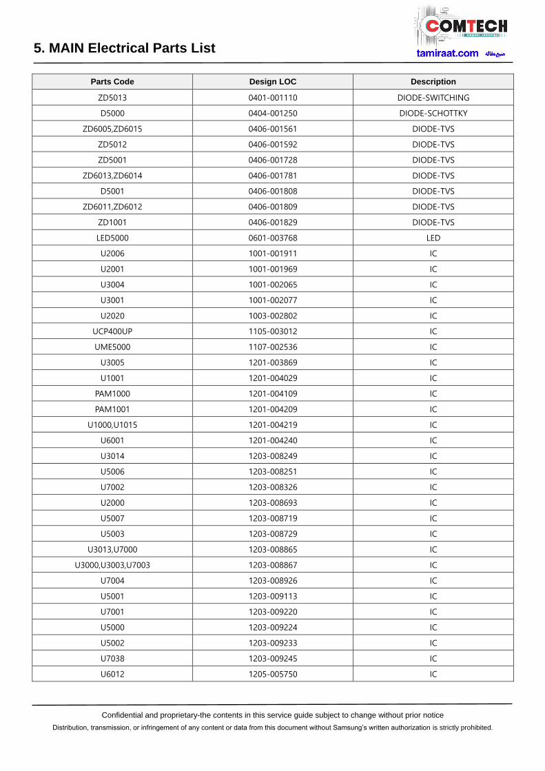
6. Level 1 Repair
14. Input SKU_CODE and BUYER, then click Save button.
※ Refer to HHPsvc→IMEI Review to check SKU Code and buyer
15. Input IMEI Number and click Apply

Confidential and proprietary-the contents in this service guide subject to change without prior notice
Distribution, transmission, or infringement of any content or data from this document without Samsung’s written authorization is strictly prohibited.
6. Level 1 Repair
16. ① Click Start → ②Input IMEI writing ID and Password & OTP → ③Input Ticket No
Model Name

Confidential and proprietary-the contents in this service guide subject to change without prior notice
Distribution, transmission, or infringement of any content or data from this document without Samsung’s written authorization is strictly prohibited.
6. Level 1 Repair
17. Connect the phone to Anyway JIG
※ When you connect the phone, the phone should be turned off.
After connecting the phone, the phone will be booted automatically.
18. IMEI Writing Proceeding
19. IMEI Writing Success
Confidential and proprietary-the contents in this service guide subject to change without prior notice
Distribution, transmission, or infringement of any content or data from this document without Samsung’s written authorization is strictly prohibited.
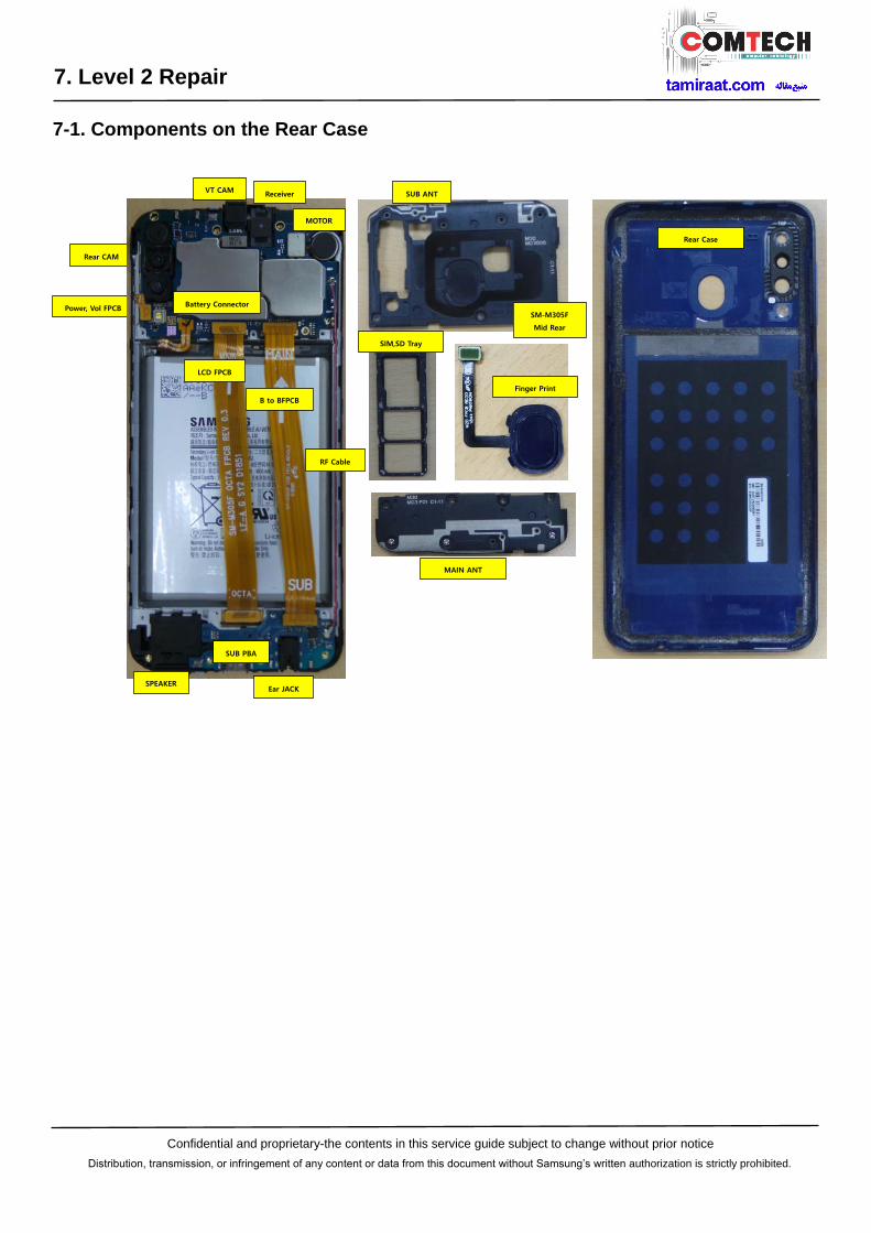
7. Level 2 Repair
7-1. Components on the Rear Case
Rear CAM
Power, Vol FPCB Battery Connector
Receiver VT CAM
MOTOR
LCD FPCB
B to BFPCB
SUB PBA
SPEAKER Ear JACK
RF Cable
SUB ANT
SM-M305F
Mid Rear
SIM,SD Tray
MAIN ANT
Rear Case
Finger Print

Confidential and proprietary-the contents in this service guide subject to change without prior notice
Distribution, transmission, or infringement of any content or data from this document without Samsung’s written authorization is strictly prohibited.
7. Level 2 Repair
7-2. Pre-requisite
Tweezers / Disass'y Stick / Screw Driver Anti-static Gloves
Anti-static Mat Hot Plate
A OCTA Disassembly Holder OCTA Disassembly Upper
Ethyl Alcohol Cotton Swab

Confidential and proprietary-the contents in this service guide subject to change without prior notice
Distribution, transmission, or infringement of any content or data from this document without Samsung’s written authorization is strictly prohibited.
7. Level 2 Repair
7-3. Parts which must be changed after repair
BOM Description & part code Image Remarks
Finger Print Tape
[GH81-17674A]
Whenever re-assemble Rear
cover at Finger Print part.
Remove old tape and use new
tape

Confidential and proprietary-the contents in this service guide subject to change without prior notice
Distribution, transmission, or infringement of any content or data from this document without Samsung’s written authorization is strictly prohibited.
7. Level 2 Repair
7-4. Disassembly
※ Caution
Be care of scratch.
※ Caution
Be care of scratch.
※ Caution
1) Be care of scratch. 2) Be care of Rear and Finger print damage.
※ Caution
Be care of Rear damage.
2 Remove Rear Cover. SIM/SD area Upper Right Below
3 Remove Finger print FPCB using tool and
detach Finger print. 4 Remove Mid Rear Screw.
1 Remove SIM/SD Tray..

Confidential and proprietary-the contents in this service guide subject to change without prior notice
Distribution, transmission, or infringement of any content or data from this document without Samsung’s written authorization is strictly prohibited.
7. Level 2 Repair
※ Caution
Be care of scratch.
※ Caution
Be careful not to damage the PBA.
※ Caution
Be care of several kinds of damage at PBA and FPCB.
※ Caution
Be careful not to damage the Camera Module.
5 Remove Mid Rear. 6 Remove 1 PBA screw.
7 Remove FPCB Connectors. Remove CAM connectors. 8

Confidential and proprietary-the contents in this service guide subject to change without prior notice
Distribution, transmission, or infringement of any content or data from this document without Samsung’s written authorization is strictly prohibited.
7. Level 2 Repair
※ Caution
Be careful not to damage the RCV.
※ Caution
Be careful not to damage the Motor.
※ Caution
Be careful scratch.
※ Caution
Be careful not to damage the Sub PBA and connector.
Detach Motor from Front Ass’y. 9 Detach RCV from Front Ass’y. 10
11 Remove Main ANT. 12 Remove B to B FPCB and Sub PBA and RF Cable.

Confidential and proprietary-the contents in this service guide subject to change without prior notice
Distribution, transmission, or infringement of any content or data from this document without Samsung’s written authorization is strictly prohibited.
7. Level 2 Repair
※ Caution
Be careful not to damage the SPK.
13 Remove SPK.

Confidential and proprietary-the contents in this service guide subject to change without prior notice
Distribution, transmission, or infringement of any content or data from this document without Samsung’s written authorization is strictly prohibited.
7. Level 2 Repair
7-5. Assembly
※ Caution
Be care of SPK damage.
※ Caution Be care of RCV damage.
※ Caution
Please keep the guide line for RF Cable.
※ Caution
Please keep the guide line for RF Cable.
1 Attach SPK on Front Ass’y. 2 Attach Sub PBA on Front Ass’y.
3 Attach RF Cable and B to B FPCB. Attach Main ANT in below area. and Screw insertion 8 points
Torque Value : 1.15kgf ±7%
4

Confidential and proprietary-the contents in this service guide subject to change without prior notice
Distribution, transmission, or infringement of any content or data from this document without Samsung’s written authorization is strictly prohibited.
7. Level 2 Repair
※ Caution
1) Be care of scratch CAM renz. 2) Be care of damage each part.
※ Caution
1) Be care of camera lenz. 2) Check for each connector connection.
※ Caution
Be care of PBA damage.
※ Caution
Be care of Tape damage.
5
8
Attach Motor and Receiver in upper area. 6 Assemble the PBA and connect FPCB.
Screw insertion 1 Point.
* Torque Value : 1.2 ±7%
7 Assemble Mid Rear and Sub ANT and screw insertion 7 point * Torque Value : 1.2 ±7%

Confidential and proprietary-the contents in this service guide subject to change without prior notice
Distribution, transmission, or infringement of any content or data from this document without Samsung’s written authorization is strictly prohibited.
7. Level 2 Repair
9 10
※ Caution
1) Be care of Finger Print FPCB damage. 2) Be care of 2 point of hook.
※ Caution
Be care of scratch Rear cover.
Assemble cover rear and insert SIM/SD Tray. Assemble Finger print module and connect FPCB.

Confidential and proprietary-the contents in this service guide subject to change without prior notice
Distribution, transmission, or infringement of any content or data from this document without Samsung’s written authorization is strictly prohibited.
8. Level 3 Repair
8-1. Components Layout
MAIN PBA (TOP SIDE)
MAIN PBA (BOTTOM SIDE)

Confidential and proprietary-the contents in this service guide subject to change without prior notice
Distribution, transmission, or infringement of any content or data from this document without Samsung’s written authorization is strictly prohibited.
8. Level 3 Repair
SUB PBA (TOP SIDE)
SUB PBA (BOTTOM SIDE)
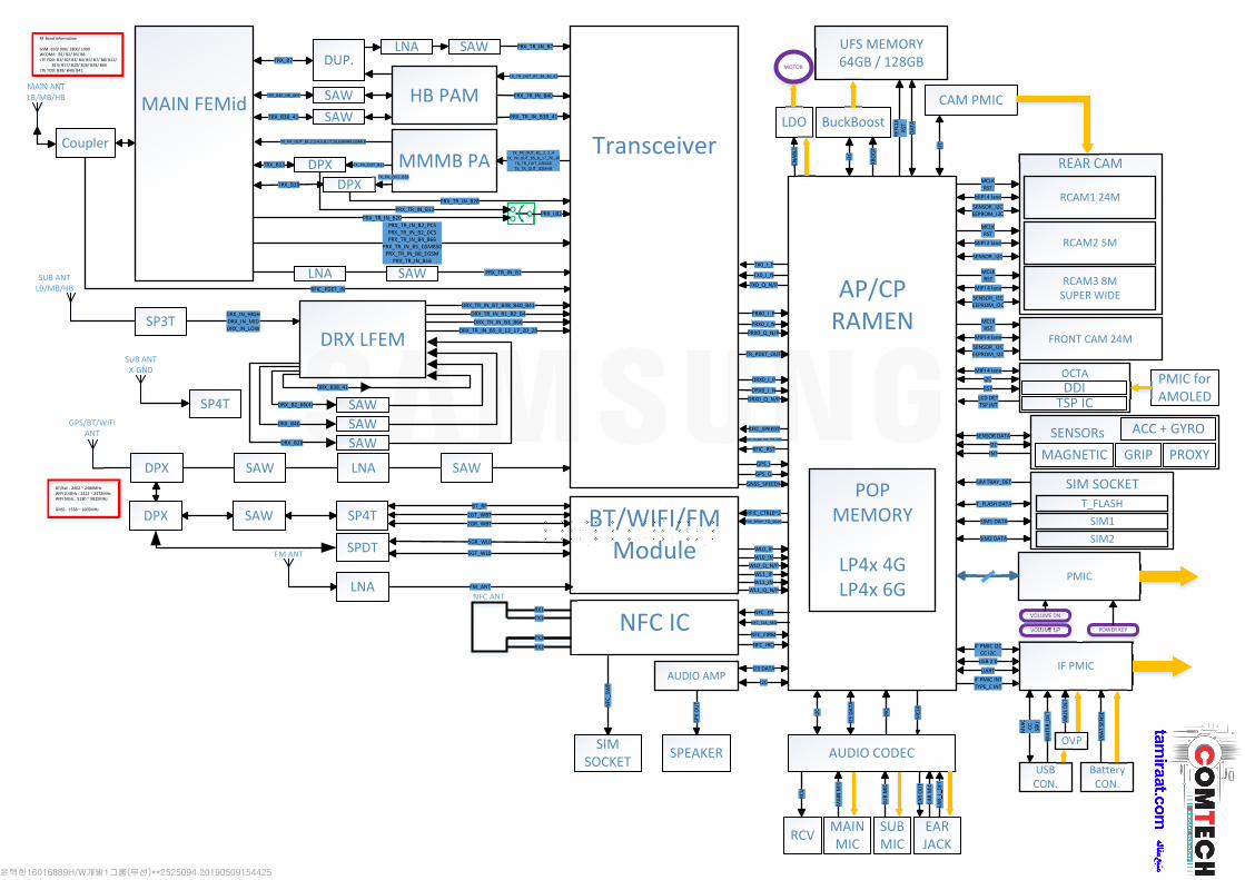
PRX_TR_IN_B1
AP/CPRAMEN
POPMEMORY
LP4x 4GLP4x 6G
Transceiver
UFS MEMORY64GB / 128GB
BuckBoost
XBOOT
I2C
DATA
CAM PMIC
REAR CAM
RCAM1 24M
I2C
MCLKRST
MIPI 4 lane
RCAM2 5M
RCAM3 8MSUPERWIDE
FRONT CAM 24M
MCLKRST
MIPI 2 lane
MCLKRST
MIPI 4 lane
SENSOR_I2CEEPROM_I2C
OCTAMIPI 4 laneI2C PMIC for
AMOLEDDDITSP IC
AUDIO CODEC
I2C
IRQ
MCLK
RCV MAINMIC
SUBMIC
EARJACK
MAINMIC
SUBMIC
RCV
EAROUT
EARMIC
EAR_
L_DE
T
IF PMIC
IF PMIC I2CCC I2CUSB 2.0UART
IF PMIC INTTYPE_C INT
USBCON.
BatteryCON.
OVP VBAT
SENSE
AUDIO AMP
SPEAKER
SPKOUT
I2S DATA
SENSORsPROXY
ACC + GYRO
MAGNETIC GRIPINTI2C
SENSOR DATA
SIM SOCKETT_FLASH
SIM TRAY_DET
SIM2 DATA
SIM1 DATA SIM1SIM2
PMIC
POWER KEYVOLUME UP
VOLUME DN
LDO
MOTOR
BT/WIFI/FMModule
NFC IC
GPS_Q
GPS_I
GNSS_SPEEDY
SAWLNASAWDPX
GPS/BT/WIFIANT
DPX SAW SP4T2GR_WBT
BT_RF2GT_WBT RFIC_CTRL0~2
WL0_INWL0_IP
WL1_IP
WL1_Q_N/P
RX1
NFC ANT
NFC_EN
NFC_CLK_REQ
NFC_IRQ
NFC_FIRM
SIMSOCKET
NFC_SWP
SPDT 5GT_WL0
LNA FM_ANT
FM ANT
TX1
TX2RX2
RFIC_RST
RFIC_SPEEDY
DRX LFEM
SAWSAWSAW
SUB ANTLB/MB/HB
DRX_B38_41
DRX_B2_66(4)
DRX_B40
DRX_B28
DRX_TR_IN_B7_B38_B40_B41DRX_TR_IN_B1_B2_B4DRX_TR_IN_B3_B66
DRX_TR_IN_B5_8_13_17_20_28SP3T
SUB ANTX‐GND
SP4T
DRX0_I_P
TR_PDET_OUT
PRX0_I_P
TX0_Q_N/P
TX0_I_P
MAIN FEMidMAIN ANTLB/MB/HB
Coupler
RFIC_PDET_IN
RF Band Information
GSM: 850/ 900/ 1800/ 1900WCDMA: B1/ B2/ B5/ B8LTE FDD: B1/ B2/ B3/ B4/ B5/ B7/ B8/ B12/
B13/ B17/ B20/ B26/ B28/ B66LTE TDD: B38/ B40/ B41
MMMB PA
HB PAM
PRX_TR_IN_B2_PCSPRX_TR_IN_B2_DCSPRX_TR_IN_B4_B66
PRX_TR_IN_B5_GSM850PRX_TR_IN_B8_EGSM
PRX_TR_IN_B16
LNA SAW
DPXDPX
PRX_TR_IN_B20PRX_LB2
PRX_TR_IN_B28
TX_PA_OUT_B28
TX_PA_OUT_B1,2,3,4,5,8,17,20,GSMHB,GSMLB
SAWSAW
DUP.LNA SAW
TRX_B7
TRX_B38_41
TX_TR_OUT_B7_38_40_41
BT/BLE : 2402 ~ 2480MHzWiFi 2.4GHz : 2412 ~ 2472MHzWiFi 5GHz : 5180 ~ 5825MHz
GNSS : 1558 ~ 1605MHz
my119.jeon
텍스트 상자
SM-M307F/FN Common

@schimatics
ANT2
013
ANT2
015
ANT5
000
ANT5
001
ANT6000 ANT6001
BH6000
BH60
01
BH60
02
BH6004
C2001
C2002
C2003 C2004
C2005
C200
6
C2009
C201
0
C2011
C201
3
C2014
C2017
C2022C2027
C203
9
C204
0
C204
1
C2043
C204
8C2
049
C205
1C2
052
C208
8
C209
1
C300
2
C3011
C3012
C3013 C301
4
C301
7
C302
4 C3029
C3032
C3034
C3035 C3036
C3038
C3039
C3042C3
046
C3048
C3053
C305
8
C3059
C306
0
C306
2
C3078
C308
2
C3095
C400
3
C401
0
C4012
C401
5C4
019
C402
0
C4024 C4025
C403
4
C405
2
C405
3C4
054
C4055
C4056
C405
7C4
064
C407
0
C5024
C5043
C5044
C5046
C5048
C5049
C5076
C507
8
C508
7
C508
8
C5089
C5127
C512
8 C6000
C6001
C6003
C600
4
C600
5
C600
6
C601
1
C601
4
C6015C6018C6019
C6020
C602
1
C602
2
C602
3
C6024
C602
5
C602
7
C6028
C6031
C603
2
C603
5
C603
9
C604
0
C604
1
C604
2
C604
3
C604
5
C6046
C604
7
C605
1
C605
2
C606
1
C608
1
C608
3
C6084
C6085
C608
6
C608
7
C6088 C608
9
C6090 C609
1C6
092
C6093
C700
0
C700
1
C700
2
C7003
C7004
C700
5
C7007
C7008
C7009
C7010
C7012
C7021
C702
2
C7025
C7035
C703
6
C703
7C7
038
C703
9
C704
2
C705
3 C7057
C705
8
C706
8
C7069
C7070
C7071
C7072C707
5
C707
8
C708
6
C7089
C709
0
C7104
C7105
C710
6
CN4000
CON6001
F2001
F200
4HDC7000
HDC7
001
HDC7
002
JTAG4001 JTAG4002
L2000
L2002
L2004
L200
5
L2006
L200
7
L200
8
L201
0
L201
1L2
012
L201
6
L202
0
L202
1
L202
9
L2032 L203
3
L203
4L2
035
L2053
L205
4
L206
5
L3011L3028L501
1L5
014
L6000
L600
1
L600
3
L600
4
L6005
L600
6
L600
8
L6013
L601
8
L700
0
L700
1
L7003
L700
4
L700
5
L700
6L7007
L700
8
L700
9
R3000
R3001
R3002
R3013
R4000
R4001
R400
2
R400
3
R400
4
R4005
R400
6
R4007
R400
8
R400
9
R401
2R4
014
R401
6
R4018
R401
9
R402
0
R402
2
R4023
R4024
R402
5
R4026
R402
7
R4030 R4032
R4034
R4035
R403
6
R4037
R4038 R4039
R404
9
R4050
R405
1
R4052
R405
3
R405
4
R4055
R4056
R4057
R4058
R4061
R4062
R4064
R5024
R600
0
R6001
R600
2
R6003
R6004
R6006
R6008
R601
2
R6014 R601
5
R602
0
R6022
R6023
R602
7R6
029
R603
1
R6035
R6038
R6994
R699
7
R7000
R7001
R700
3
R7034
SC6000
SC60
01
SC60
02
SC60
04
SIM601 SIM602
SIM
603
SIM604UPTH4000
TP_3000
TP_3002
TP_UB
TP_XCP_RF_ON4000
TP_XGNSS_GPLL_ANA_EXT
TP_XOM0 TP_XOM2
TP_XRSTOUT_N
TP2002
TP3001TP3002TP3003TP3004
TP3005 TP3006
TP30
07
TP3008
TP3009
TP30
10
TP30
12
TP3013
TP4000
TP5000
TP5001
TP5002TP5003
TP5004
TP5006
TP5007
TP50
12
TP5014
TP5015
TP5016
TP6000 TP6001TP6002TP6003
TP6007
TP6022TP6024
TP6999
U2000
U2001
U201
2
U3000
U3002
U3012
U3014
U301
6U5006
U600
1
U601
2
U703
8
UCP4
00
XCP_GPIO4000
ZD50
13
ZD60
00ZD
6001
ZD60
06
ZD60
07 ZD6008
ZD60
09
ZD60
10
ZD60
16
ZD6019
ZD60
21ZD6022
ZD60
23
ZD6024
ZD6025
ZD60
26
ZD6027
ZD70
00
ZD7001
VX_Setup(2018-12-18)_HHPCreated date of PCB data : 2019/7/22 19:01:27
Model : Revision : Manufacture Count : Charge : Contact : Date : Routing : Resin :
VX_Setup(2018-12-18)_HHPCreated date of PCB data : 2019/7/22 19:01:27
my119.jeon
텍스트 상자
SM-M307F/FN Common

@schimatics
ANT2000 ANT2002
ANT3
001
ANT3
002
ANT3
003
C1000
C1001
C1002
C1003
C1004
C100
5
C100
6
C100
7
C1008
C100
9
C1010
C101
1
C1012
C1014
C101
5
C101
7
C101
8
C1021 C1022
C102
4
C1028
C102
9
C103
2
C103
3
C1034
C103
5
C1036 C1037
C103
8 C1039
C104
0
C104
2
C104
3
C104
4
C1045
C1046
C104
7
C104
8
C1049
C105
0
C105
1
C1052
C105
3
C105
4
C1056 C1057
C1058
C1059
C1060
C1061
C1062C1063
C106
4
C106
5
C106
6
C106
7C1
068
C106
9
C107
0
C107
3
C107
4
C107
5
C1076
C1077
C1085
C109
2
C109
5
C109
6
C109
7
C109
8
C109
9
C1102
C110
3
C110
4
C1105
C1106
C110
7
C1108
C1109C111
0
C111
1C1
112
C111
4
C2000
C200
7
C200
8
C201
5C2
018
C202
0
C2021
C202
3
C202
4
C2025
C2026
C202
8
C202
9
C2030
C2031
C2032
C2033
C203
4
C203
5
C203
6
C203
7
C203
8
C2042
C204
4
C204
5
C205
0
C205
3
C2072
C2095
C209
7
C2098
C210
0
C210
1
C3000
C300
1
C3003
C300
4
C3005
C300
6
C3007
C300
8
C300
9
C3010
C3015
C301
6
C3018
C301
9
C302
0
C3021
C302
2
C302
3
C3025C3026
C302
7
C3028
C303
0
C3031
C3033
C303
7
C3040C3041
C3050
C305
2
C305
4
C3055
C305
7
C307
7C307
9
C308
0
C308
1
C308
7
C3090
C309
7
C4000
C4001
C4002
C4004
C400
5C4
006
C4007
C4008
C400
9
C401
1
C4013
C4014
C401
6
C4017C4018
C4021
C4022
C402
3
C402
6
C402
7
C402
8
C402
9
C403
0
C403
1
C403
2
C403
3
C403
6
C403
7C4
038
C403
9
C4040C4041
C4042
C404
3
C404
4
C404
5
C4046
C404
7
C4048
C404
9
C4050
C4051
C4058
C4059
C4060
C4061
C4062
C406
3
C4065
C4066
C4067
C406
8C4069
C4071
C4072C4073 C4074
C407
5
C4076
C407
7
C407
8
C407
9
C408
0
C408
1
C4082C4083
C4084
C4085
C4086
C408
7
C408
8
C4089
C409
0
C4091
C409
2
C409
3
C409
4
C409
5
C409
6
C409
7
C409
8
C4099
C410
0
C4101
C4102
C500
0
C500
1
C5002
C5003
C500
4
C5005
C500
6
C5008
C5009
C501
0
C501
1
C501
2
C5013
C5014
C5015
C5016
C501
7
C5018
C5019
C5020
C5021
C502
2
C5023
C502
5
C5026C5
027
C5028C5029
C5030
C503
1
C503
2
C503
3
C503
4
C503
5
C503
6
C503
7
C5038
C5039
C504
0
C504
1
C5042
C5047
C505
0
C505
1
C5052
C505
3
C505
4
C505
5C5
056
C5057
C5058
C505
9
C5060
C506
1
C506
2
C506
3C5064C5
065
C506
6
C506
7
C5068
C506
9
C507
0
C507
1
C507
2
C5073
C507
4
C507
5
C5077
C507
9
C508
0
C508
1
C508
2
C5083
C508
4
C508
5
C5086
C509
0
C509
1
C509
2
C509
3
C5094C5
095
C509
6
C5097
C5098
C509
9
C5100
C5101
C510
2
C5103
C510
4
C5105
C5106
C5107
C5108
C510
9C5
110
C511
1
C5112
C511
3
C511
4
C5115
C511
6
C511
7
C5118
C5125
C5126
C5129
C513
0
C513
5
C513
6
C513
7
C513
8
C5139
C5141
C5142
C5143
C5144
C5998
C5999
C6002
C600
8
C600
9 C6010
C601
2
C601
3
C601
6
C601
7
C602
6
C602
9
C6030
C603
7
C605
9
C6082
C700
6
C701
3
C701
4
C701
5
C7016
C701
8
C7019
C7020
C702
3
C7024
C702
7
C7028C7029
C703
0
C703
1
C7032 C703
3
C7034
C704
0
C704
1C7
045
C704
6
C704
7C7048
C7049
C7050
C7051
C705
2
C707
6
C707
7
C707
9
C7080
C708
1
C708
2
CLIP
1000
CON6
000
D500
0
D500
1
DN_L
AY8
DP_L
AY8
F100
0
F100
1
F100
2F1003
F100
6F1009
F3000
F3001
F300
2
F3003
F3004
GA70
00
HEA4000HEA6000
HEA7003
L100
0
L1002
L100
3
L100
4
L100
5
L100
6
L100
7
L100
8
L100
9
L101
0
L101
1
L101
4
L1016
L101
7
L101
8
L101
9
L102
2
L1023
L1025
L1026
L1027L1028
L1029
L103
0
L1031
L103
2
L1033
L103
4
L103
5
L103
6
L103
7
L103
8
L104
0L1
041
L104
2
L104
3
L104
4
L104
5
L104
7
L104
9
L105
0
L105
1
L105
2
L1053
L105
5
L105
6
L106
0
L106
2L1
063
L106
6
L106
9L1
070
L107
3
L107
4
L108
1
L1082L2
001L2003
L2009
L201
3
L201
4
L201
5
L2017
L2022
L2023
L2024
L2026
L202
7
L202
8
L2030
L203
1L2
036
L203
7
L2038
L204
0
L2048
L204
9
L206
6
L3000
L300
1
L300
2
L300
3
L3005
L3006
L300
7
L3008
L300
9
L301
0
L301
2
L3013
L301
4
L3015
L3016
L301
7
L3018
L3020
L302
6
L3027
L3034
L500
0
L500
1
L500
2
L500
3
L500
4
L500
5
L500
6
L500
7
L500
8
L5009
L501
0
L5012
L501
3
L5015
L501
6
L5020
L6002
L6007
L6011
L601
2
L601
4
L6015
L700
2 L7010LE
D500
0
MIC6000
OSC2000
OSC5
000
PAM1000
PAM
1001
R1000
R1001R1002
R1003
R1004
R100
5
R1006
R2001
R301
1
R301
2
R4011
R4013
R4021
R402
8
R4029
R403
1
R4033
R404
0
R404
1
R404
2
R4043
R404
4
R4045
R4047
R4063
R4065
R5000
R500
1
R5002
R500
3
R500
4
R500
5
R500
6
R500
7
R500
8
R5009
R501
0
R5011
R501
2R5014
R5020
R502
1
R5022
R5023
R5028R5029
R505
2
R6005
R6007
R600
9
R6010
R6011
R6013
R601
6
R601
7
R6018
R6019R6021
R6024
R6026
R6028
R603
4
R7002
R701
1
RFIC
_CTR
L300
0RF
IC_C
TRL3
001
RFIC
_CTR
L300
2
RFS1000
SC6003
SC60
05
SC6006
SOC5
000
SOC5001
SOC5002
SOC7004
TH1000
TH4001
TH5000
TP_F
EM_C
TRL3
000
TP_F
EM_C
TRL3
001
TP_F
EM_C
TRL3
002
TP_UFS_RX_N
TP_UFS_RX_P
TP_U
FS_T
X_N
TP_U
FS_T
X_P
TP10
00
TP10
01
TP2000 TP2001
TP30
00
TP30
11
TP3015
TP40
11
TP5005
TP5008
TP5009
TP5010
TP50
11
TP5013
TP5017
TP7001
U1000
U1001
U100
2U1
015
U200
6
U201
6
U2020
U3001
U3003
U3004
U3005
U301
3
U301
5
U3018
U5000
U500
1
U5002
U5003
U5007
U700
0
U7001
U7002
U7003
U700
4
U7035
UME5000
VR70
00
WL_
PDET
3001
ZD1001
ZD10
02
ZD30
00ZD
3001
ZD5000
ZD5001
ZD5002
ZD50
03
ZD5004
ZD50
05
ZD50
06
ZD5007
ZD5010
ZD5011
ZD50
12
ZD5014 ZD6002
ZD6003
ZD60
05
ZD6011
ZD6012
ZD6013ZD6014ZD6015
ZD60
17
ZD60
18
ZD6030
ZD70
02
ZD70
04
ZD70
05
ZD70
06
ZD70
07
VX_Setup(2018-12-18)_HHPCreated date of PCB data : 2019/7/22 19:01:27
Model : Revision : Manufacture Count : Charge : Contact : Date : Routing : Resin :
VX_Setup(2018-12-18)_HHPCreated date of PCB data : 2019/7/22 19:01:27

Confidential and proprietary-the contents in this service guide subject to change without prior notice
Distribution, transmission, or infringement of any content or data from this document without Samsung’s written authorization is strictly prohibited.
8. Level 3 Repair
8-3. Flow chart of Troubleshooting.
Oscilloscope Digital Multimeter
Power Supply + driver, ESD Safe Tweezer
8960 & Spectrum Analyzer Soldering iron

Confidential and proprietary-the contents in this service guide subject to change without prior notice
Distribution, transmission, or infringement of any content or data from this document without Samsung’s written authorization is strictly prohibited.
8. Level 3 Repair
8-4-1. Power On
Mobile phone does not power on.
YesNo
Yes
Change the FRONT-LCD ASSY
Replace the Power key FPCB
YesNo
Check the signal of TRST_N = 1.8V
No
Check the output voltage of U5000
L5000 > 0.75V, L5001 > 0.75V, L5002
> 0.75V,
L5003 > 0.75V, L5004 > 0.75V, L5005
> 0.75V,
L5006 > 0.75V, L5007 > 1.1V, L5008
> 1.3V, L5009 > 2.0V, L5010 > 0.75V
and other LDO Voltage
If the output voltage is not normal,
Change the U5000
※ Each voltage level has ±10% margin
YesNo
Check the Clock OSC5000Is the frequency 32.768kHz?
No Replace the OSC5000
※ Test condition (Oscilloscope setting)
: 20.0us.div (time division) YesNo
Check the initial operation
YesNo
No Charging the battery by TA.
If its voltage level is extremely low
(under 3.0V),
Change the battery.
END
YesNo
Power-on the phone and check
the power-on sound
or motor Vibration. Sound or Vibration is ok?
No
Check the voltage level at R5023 while pressing power
key. Is the voltage high?
No
Check the Battery Voltage. Is it more than 3.8V?

Confidential and proprietary-the contents in this service guide subject to change without prior notice
Distribution, transmission, or infringement of any content or data from this document without Samsung’s written authorization is strictly prohibited.
8. Level 3 Repair
8-4-2. Initial
Initial Failure
YesNo
YesNo
END
AbnormalNo
Re Check "Power on"Trouble shooting process
Abnormal Check the OSC5000 (Crack, open etc.) Check the U5000 (Crack etc)
Normal
Change U5000
Re-download latest SW on the mobile phone
Abnormal
Change PBA

Confidential and proprietary-the contents in this service guide subject to change without prior notice
Distribution, transmission, or infringement of any content or data from this document without Samsung’s written authorization is strictly prohibited.
8. Level 3 Repair
8-4-3. No Service
No service
YesNo
YesNo
END
Check the Voltage L5008 : 1.3V, C5084 : 1.3V
No
Replace the U5000
Home screen → Phone →
Keypad → *#1234# → Check
Phone version → CP :
N950FXXXX or unkown
YesNo
CP : A505XXXXX
Check the connection of RF coaxial cable
Check the clock OSC5000 Is the frequency 32.768KHz?
No
YesNo
Replace the OSC5000
Replace the U2016
YesNo

Confidential and proprietary-the contents in this service guide subject to change without prior notice
Distribution, transmission, or infringement of any content or data from this document without Samsung’s written authorization is strictly prohibited.
8. Level 3 Repair
8-4-4. SIM Part
Insert SIM card
YesNo
YesNo
END
Check the SIM Voltage. = 1.8V or 3.0V
(C6019,C6022)?
No
Change to the new SIM card.
If it doesn`t still work SIM card after
changing
the SIM card, Check the U5000 (Crack
etc)
Is SIM socket ok?
YesNo
No
Replace SIM socket
Check the SIM RST / IO / CLK. (SIM1 : ZD6024, ZD6022, ZD6023) (SIM2 : ZD6027, ZD6025, ZD6026)
Is signal ok?
No
YesNo
Check the UCP400 (Crack etc)
Confidential and proprietary-the contents in this service guide subject to change without prior notice
Distribution, transmission, or infringement of any content or data from this document without Samsung’s written authorization is strictly prohibited.
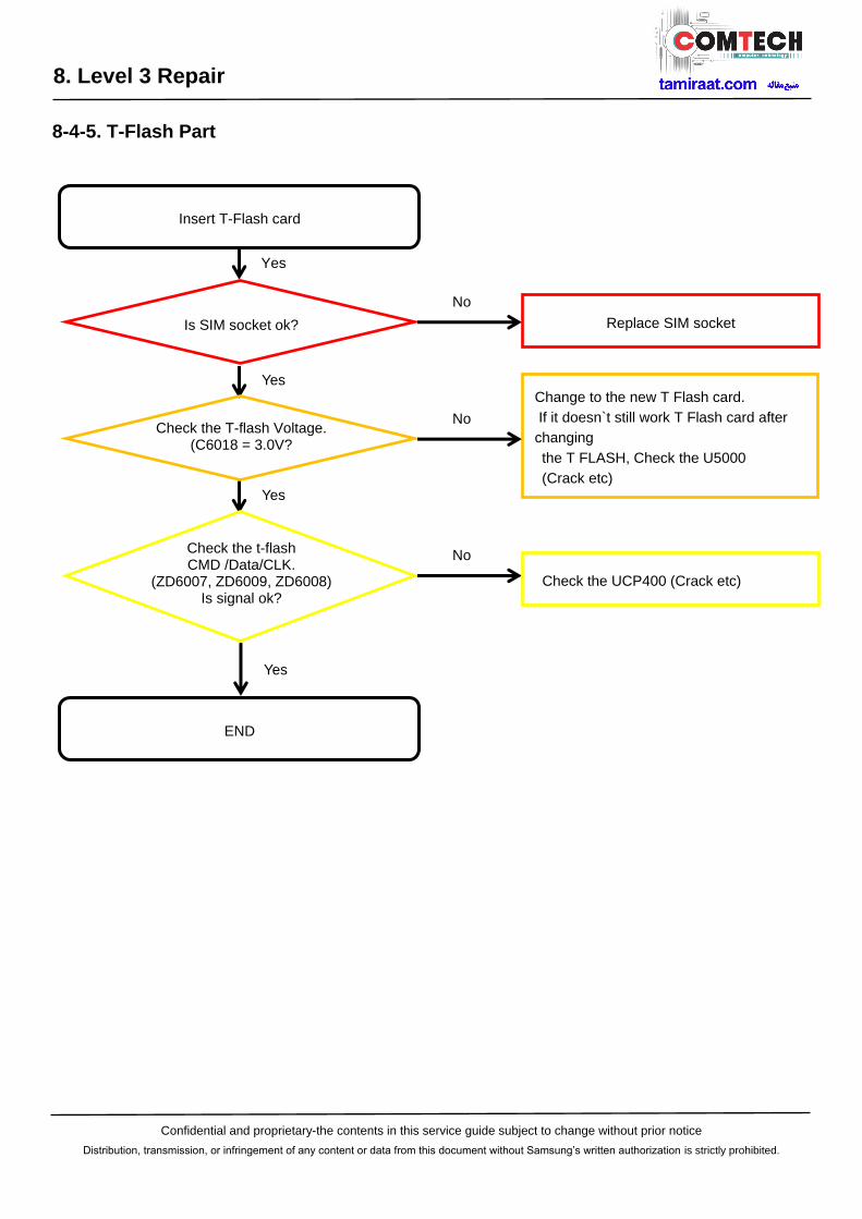
8. Level 3 Repair
8-4-5. T-Flash Part
Insert T-Flash card
YesNo
YesNo
END
Check the T-flash Voltage.(C6018 = 3.0V?
No
Change to the new T Flash card.
If it doesn`t still work T Flash card after
changing
the T FLASH, Check the U5000
(Crack etc)
Is SIM socket ok?
YesNo
No
Replace SIM socket
Check the t-flash CMD /Data/CLK.
(ZD6007, ZD6009, ZD6008) Is signal ok?
No
YesNo
Check the UCP400 (Crack etc)
Confidential and proprietary-the contents in this service guide subject to change without prior notice
Distribution, transmission, or infringement of any content or data from this document without Samsung’s written authorization is strictly prohibited.
8. Level 3 Repair
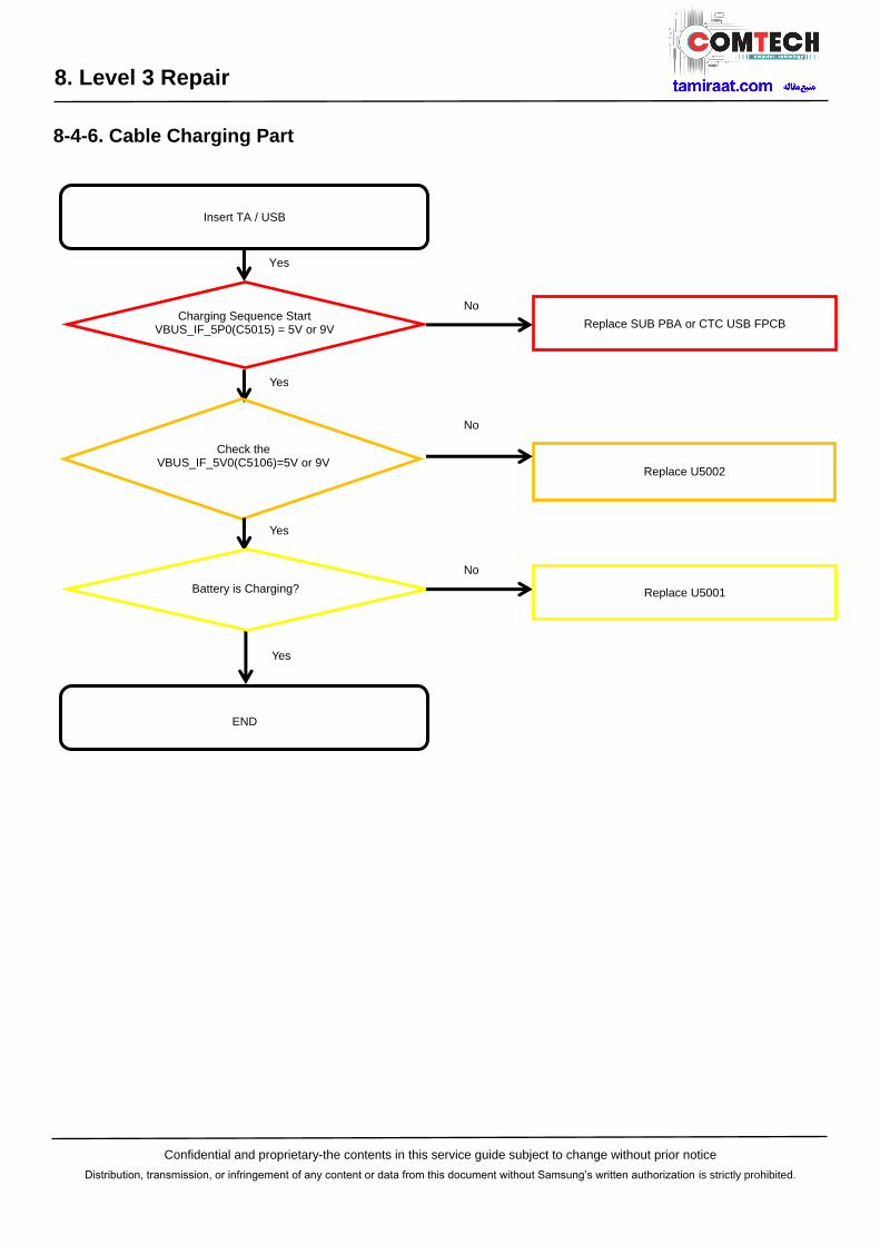
8-4-6. Cable Charging Part
Insert TA / USB
Yes
Yes
END
Check the VBUS_IF_5V0(C5106)=5V or 9V
No
Replace U5002
Charging Sequence Start VBUS_IF_5P0(C5015) = 5V or 9V
Yes
No
Replace SUB PBA or CTC USB FPCB
Battery is Charging?
No
Yes
Replace U5001

Confidential and proprietary-the contents in this service guide subject to change without prior notice
Distribution, transmission, or infringement of any content or data from this document without Samsung’s written authorization is strictly prohibited.
8. Level 3 Repair
8-4-7. OTG
OTG does not work
Yes
Yes
END
Check the VBUS_IF_5P0(C5105) = 5V
No Check U5002
(crack, open, damaged, etc.)
Check the VBUS_IF_5P0(C5095) = 5V
Yes
No Check U5001
(crack, open, damaged, etc.)
Check OTG working ?
No
Yes
Replace SUB PBA or CTC USB FPCB

Confidential and proprietary-the contents in this service guide subject to change without prior notice
Distribution, transmission, or infringement of any content or data from this document without Samsung’s written authorization is strictly prohibited.
8. Level 3 Repair
8-4-8-1. Magnetic Sensor
Magnetic Sensor does not work
YesNo
YesNo
END
Check R3011, R3012 (I2C is OK?)
No
Replace U3018
Check the voltage C3033 =1.8V
YesNo
No
Replace U3003

Confidential and proprietary-the contents in this service guide subject to change without prior notice
Distribution, transmission, or infringement of any content or data from this document without Samsung’s written authorization is strictly prohibited.
8. Level 3 Repair
8-4-8-2. 6Axis Sensor
6Axis Sensor does not work
YesNo
YesNo
END
Check 6Axis SENSOR_SPI pin
(SPI is OK?)
No
Replace U3012
Check the voltage C3029 = 1.8V
YesNo
No
Replace U3003

Confidential and proprietary-the contents in this service guide subject to change without prior notice
Distribution, transmission, or infringement of any content or data from this document without Samsung’s written authorization is strictly prohibited.
8. Level 3 Repair
8-4-8-3. Proximity
Proximity Sensor does not work
YesNo
No
Replace U3014
Check the voltage C3038 =1.8V
(Sensor’s IO voltage)
YesNo
No
Replace U3003
No
YesNo
Replace U3016
Check the voltage C3062 =3.3V
(Sensor’s LED voltage)
Check SDA, SCL of U3016 (I2C is OK?)
YesNo
END

Confidential and proprietary-the contents in this service guide subject to change without prior notice
Distribution, transmission, or infringement of any content or data from this document without Samsung’s written authorization is strictly prohibited.
8. Level 3 Repair
8-4-8-4. Fingerprint Sensor
END
Replace the Fingerprint sensor module
And Calibration
YesNo
Fingerprint Sensor does not work
YesNo
No
Check Finger sensor Connector. Is it broken?
YES
Replace Finger Sensor
Do you change Main PCB or Finger sensor?
No
YES
Do calibration.
Check the Fingerprint Sensor SPI Line and VCC 3.3V.
(They are OK?)
No
No
Replace Main PCB

Confidential and proprietary-the contents in this service guide subject to change without prior notice
Distribution, transmission, or infringement of any content or data from this document without Samsung’s written authorization is strictly prohibited.
8. Level 3 Repair
8-4-9-1. Microphone Part - Main MIC
Check main microphone function
in voice call Handset mode or voice recorder
mode
YesNo
Check the voltage of L9015 at board = 2.7V
No replace MAIN FPCB
YesNo
END
Check the MAIN_MIC_P data at L9016
YesNo
Replace MIC9000 No

Confidential and proprietary-the contents in this service guide subject to change without prior notice
Distribution, transmission, or infringement of any content or data from this document without Samsung’s written authorization is strictly prohibited.
8. Level 3 Repair
8-4-9-2. Microphone Part - Sub(2nd) MIC
Check Sub(2nd) microphone function
in voice call loudSPK mode
or in camcording mode
mode
YesNo
Check the voltage atL6012 = 2.8V
No Replace U6012
YesNo
END
Check theSUB_MIC_P data at
L6015
YesNo
No Replace MIC6000

Confidential and proprietary-the contents in this service guide subject to change without prior notice
Distribution, transmission, or infringement of any content or data from this document without Samsung’s written authorization is strictly prohibited.
8. Level 3 Repair
8-4-10. Speaker Part
Check speaker function.
Play MP3 with maximum volume level.
YesNo
Check C-clips of Sub PBAANT9002, ANT9003
No Replace C-Clip
YesNo
YesNo
END
Replace speaker module
No Replace MAIN FPCB
Check the PWM output at ANT9002,ANT9003
Check the PWM output at ANT9002,ANT9003
Replace SUB PBA
Check the PWM output at ANT9002,ANT9003
Replace U6001 on MAIN PCB
YesNo
YesNo
YesNo
No
No

Confidential and proprietary-the contents in this service guide subject to change without prior notice
Distribution, transmission, or infringement of any content or data from this document without Samsung’s written authorization is strictly prohibited.
8. Level 3 Repair
8-4-11. Receiver Part
Check receiver function
in voice call receiver mode
YesNo
Check RCV module where RCV's placed
for any damage
No Resolder or Replace
ANT6000, ANT6001
YesNo
Check the signals onL6001, L6003
No Resolder or replace L6001, L6003
YesNo
END
Replace RCV module
YesNo

Confidential and proprietary-the contents in this service guide subject to change without prior notice
Distribution, transmission, or infringement of any content or data from this document without Samsung’s written authorization is strictly prohibited.
8. Level 3 Repair
8-4-12. BT/WIFI
BT/WIFI is not working
YesNo
No Enable BT or WIFI function.
YesNo
END
YesNo
No Resolder or change
ANT3003, C3008,L3014,C3040, L3013,F3003,C3027,F3004
YesNo
No Resolder or change C3087,L3001,L3018,C3025,
C3023,L3002,C3020,L3026,C3019, L3034,C3037,C3016
Resolder or change U3015
Check BT or WIFI function ON
YesNo
YesNo
Resolder or Replace of F3000,U3001,U3004
No
YesNo
Check ANT Path ANT3003, C3008,L3014,C3040,
L3013,F3003,C3027,F3004
Check RF path C3087,L3001,L3018,C3025,
C3023,L3002,C3020,L3026,C3019, L3034,C3037,C3016
Check the Status F3000,U3001,U3004

Confidential and proprietary-the contents in this service guide subject to change without prior notice
Distribution, transmission, or infringement of any content or data from this document without Samsung’s written authorization is strictly prohibited.
8. Level 3 Repair
8-4-13. GPS
GPS is not working
YesNo
No Enable GPS Function in the setting.
YesNo
END
YesNo
No Resolder or change
ANT3003,C3008,L3014,
C3040,L3013,F3003
YesNo
No Resolder or change L3003,C3077,C3052,C3028,L3009,L3005, C3030,L3007,L3016,C3031,L3008,L3017
YesNo
Resolder or change U2016
Check GPS function ON
Resolder or change F3001,U3005,F3002
No
Check Antenna path
ANT3003,C3008,L3014,
C3040,L3013,F3003
Check RF Path L3003,C3077,C3052,C3028,L3009,L3005, C3030,L3007,L3016,C3031,L3008,L3017
Check RF ComponentF3001,U3005,F3002
Replace the OSC2000
No
YesNo
YesNo
Check 26MHz Clock at output of OSC2000
of OSC4000

Confidential and proprietary-the contents in this service guide subject to change without prior notice
Distribution, transmission, or infringement of any content or data from this document without Samsung’s written authorization is strictly prohibited.
8. Level 3 Repair
8-4-14. NFC [SM-M307FN)
END
NFC is not working
YesNo
No Enable NFC Function
Check the Voltage on
C3082 = 1.8V
YesNo
YesNo
No Resolder or change
ANT3001, ANT3002
YesNo
No Check U3002
(crack, open, damaged, etc.)
YesNo
No
No
Check UCP400
Resolder or change C3054,C3053,C3024,C3058, C3013,C3014,L3011,L3028, C3048,R3013,C3059,R3000
YesNo
YesNo
Resolder or Replace U3002
Check NFC function ON
Check the Antenna contact
ANT3001, ANT3002
Check 26MHz Clock at TP3011
Check the Status of C3054,C3053,C3024,C3058, C3013,C3014,L3011,L3028, C3048,R3013,C3059,R3000

Confidential and proprietary-the contents in this service guide subject to change without prior notice
Distribution, transmission, or infringement of any content or data from this document without Samsung’s written authorization is strictly prohibited.
8. Level 3 Repair
8-4-15. FM radio part
FM is not working
YesNo
No Enable FM Function.
YesNo
END
YesNo
No Resolder or change
C6030,HEA6000,C3003,L3006
YesNo
No Resolder or change
C9000,L9000,C9034,C9004,U9002,
C9018,L9018,C9019
Resolder or Replace U3015
YesNo
Check the FM function
Check the MAIN PBA
C6030,HEA6000,C3003,L3006
Check the SUB PBA
C9000,L9000,C9034,C9004,U9002,
C9018,L9018,C9019

Confidential and proprietary-the contents in this service guide subject to change without prior notice
Distribution, transmission, or infringement of any content or data from this document without Samsung’s written authorization is strictly prohibited.
8. Level 3 Repair
8-4-16. Display
LCD is still off after PWR ON
YesNo
No Reconnect the SOC7004
END
YesNo
Check VDD_LCD_3P0 = 3.0V (C7081) VDD_LCD_1P8 = 1.8V (C7082)
No Resolder or Replace the U7002(3.0V)Resolder or Replace the U7003(1.8V)
YesNo
Check ELVDD 4P6 = 4.6V (C7079)
ELVSS_-4P4 = - 4.4 ~ - 1.4V (C7078) ELAVDD_7P3 = 7.6V (C7080)
No Resolder or Replace the U7038
YesNo
Check the connection of SOC7004
Replace the Display module
YesNo
Replace the Display con-to-con FPCB
YesNo
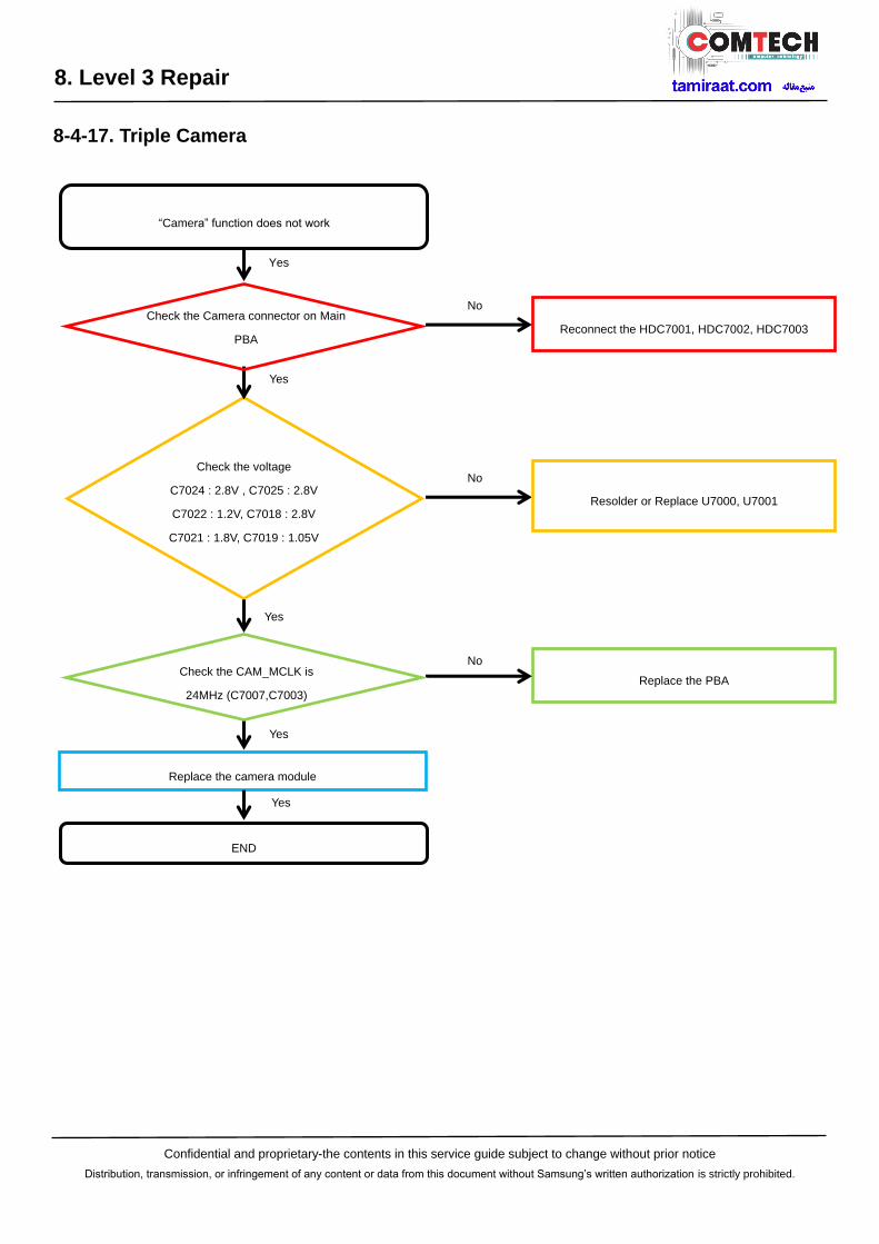
Confidential and proprietary-the contents in this service guide subject to change without prior notice
Distribution, transmission, or infringement of any content or data from this document without Samsung’s written authorization is strictly prohibited.
8. Level 3 Repair
8-4-17. Triple Camera
Yes
END
Check the voltage
C7024 : 2.8V , C7025 : 2.8V
C7022 : 1.2V, C7018 : 2.8V
C7021 : 1.8V, C7019 : 1.05V
No
Yes
No
Replace the PBA
“Camera” function does not work
Yes
No
Reconnect the HDC7001, HDC7002, HDC7003
Yes
Check the Camera connector on Main
PBA
Yes
Replace the camera module
Check the CAM_MCLK is
24MHz (C7007,C7003)
Resolder or Replace U7000, U7001

Confidential and proprietary-the contents in this service guide subject to change without prior notice
Distribution, transmission, or infringement of any content or data from this document without Samsung’s written authorization is strictly prohibited.
8. Level 3 Repair
8-4-18. VT CAMERA
“Camera” function does not work
Yes
No
Reconnect the HEA7003
Yes
END
Yes
Check the voltage
C7023 : 2.8V
C7020 : 1.05V
No
Resolder or Replace U7001
Yes
No
No
Replace the PBA
Yes
Replace the Front camera module
Check the Camera connector on Main
PBA
Check the VTCAM_MCLK is
24MHz (R7034)

Confidential and proprietary-the contents in this service guide subject to change without prior notice
Distribution, transmission, or infringement of any content or data from this document without Samsung’s written authorization is strictly prohibited.
8. Level 3 Repair
8-4-19. TSP
Touch Screen does not work
YesNo
No Reconnect the SOC7004
YesNo
END
YesNo
Check the voltage VDD_TSP_A3P0 (C7077) = 3.0V
No Resolder or Replace U7004
YesNo
Replace the Display module
Check TSP Connector on MAIN PBA
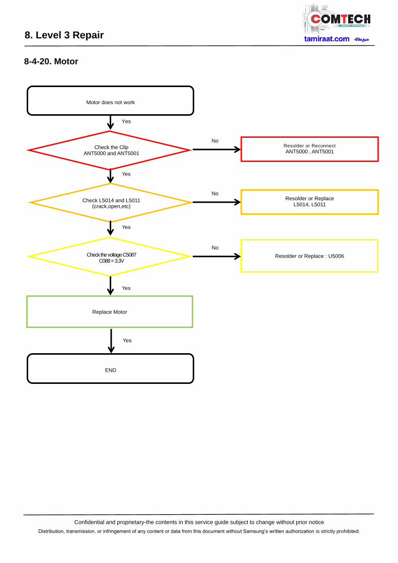
Confidential and proprietary-the contents in this service guide subject to change without prior notice
Distribution, transmission, or infringement of any content or data from this document without Samsung’s written authorization is strictly prohibited.
8. Level 3 Repair
8-4-20. Motor
Motor does not work
Yes
No Resolder or Reconnect ANT5000 , ANT5001
Yes
END
Yes
Check L5014 and L5011 (crack,open,etc)
No Resolder or Replace
L5014, L5011
Yes
No
Resolder or Replace : U5006
Yes
Replace Motor
Check the Clip ANT5000 and ANT5001
Check the voltage C5087 C088 = 3.3V

Confidential and proprietary-the contents in this service guide subject to change without prior notice
Distribution, transmission, or infringement of any content or data from this document without Samsung’s written authorization is strictly prohibited.
8. Level 3 Repair
8-4-21. GSM 850/900, WCDMA B5/8, LTE B5/8/20 PRx
END
Check ant path any damage(ANT9101 ~ ANT9009)
Is it ok? (SUB PBA) )
Check RX path any damage(RFS1000~U1002)
Is it ok?
Check U2016 any damage
(Crack, open, etc), is it ok?
i
Change the board
Resolder or changeAntenna path components
Resolder or change RX path components
Resolder or change RX path components
NO
NO
NO
YES
YES
YES
YES
YES
It is not catching the channel In normal condition

Confidential and proprietary-the contents in this service guide subject to change without prior notice
Distribution, transmission, or infringement of any content or data from this document without Samsung’s written authorization is strictly prohibited.
8. Level 3 Repair
8-4-22. LTE B7/38/40/41 PRx
END
Check ant path any damage(ANT9101 ~ ANT9009)
Is it ok? (SUB PBA) )
Check RX path any damage(RFS1000~U1002)
Is it ok?
Check PAM1000~U2016 any damage
(Crack, open, etc), is it ok?
i
Change the board
Resolder or changeAntenna path components
Resolder or change RX path components
Resolder or change RX path components
NO
NO
NO
YES
YES
YES
YES
YES
It is not catching the channel In normal condition

Confidential and proprietary-the contents in this service guide subject to change without prior notice
Distribution, transmission, or infringement of any content or data from this document without Samsung’s written authorization is strictly prohibited.
8. Level 3 Repair
8-4-23. GSM DCS/PCS, WCDMA B1/2, LTE B1/3 PRx
END
Check ant path any damage(ANT9101 ~ ANT9009)
Is it ok? (SUB PBA) )
Check RX path any damage(RFS1000~U1002)
Is it ok?
Check U1002~U2016 any damage
(Crack, open, etc), is it ok?
i
Change the board
Resolder or changeAntenna path components
Resolder or change RX path components
Resolder or change RX path components
NO
NO
NO
YES
YES
YES
YES
YES
It is not catching the channel In normal condition
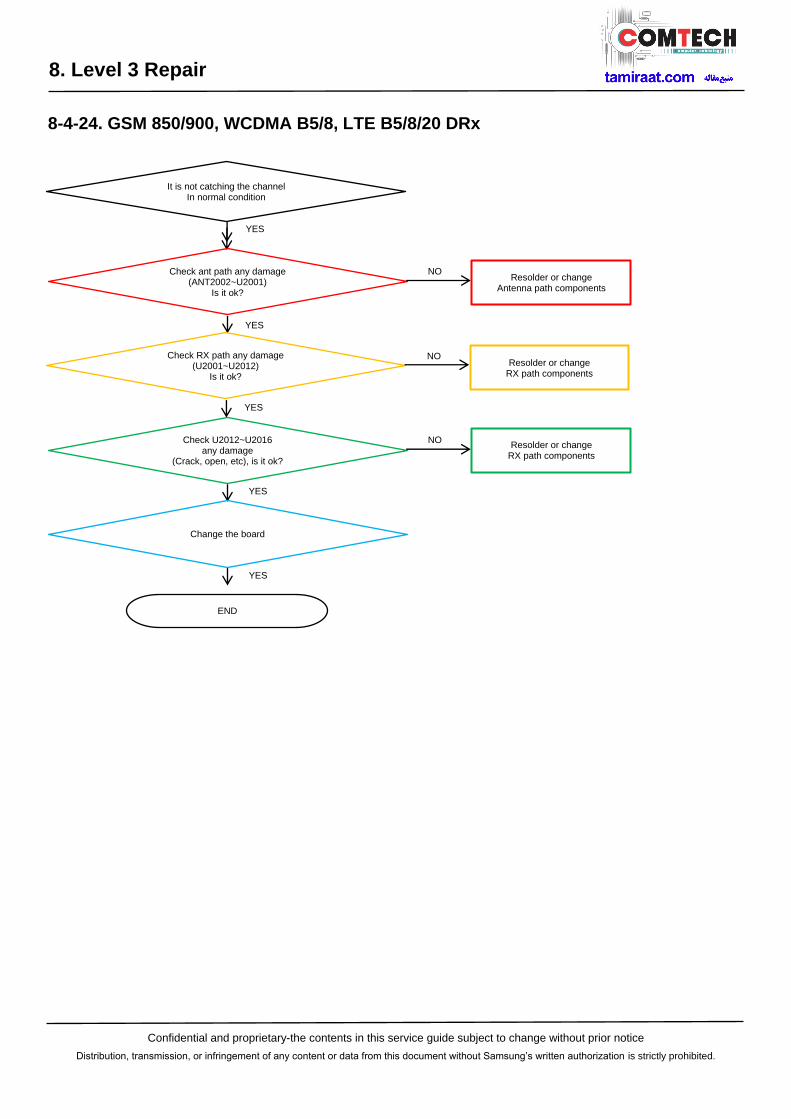
Confidential and proprietary-the contents in this service guide subject to change without prior notice
Distribution, transmission, or infringement of any content or data from this document without Samsung’s written authorization is strictly prohibited.
8. Level 3 Repair
8-4-24. GSM 850/900, WCDMA B5/8, LTE B5/8/20 DRx
END
Check ant path any damage(ANT2002~U2001)
Is it ok? )
Check RX path any damage(U2001~U2012)
Is it ok?
Check U2012~U2016any damage
(Crack, open, etc), is it ok?
i
Change the board
Resolder or changeAntenna path components
Resolder or change RX path components
Resolder or change RX path components
NO
NO
NO
YES
YES
YES
YES
YES
It is not catching the channel In normal condition

Confidential and proprietary-the contents in this service guide subject to change without prior notice
Distribution, transmission, or infringement of any content or data from this document without Samsung’s written authorization is strictly prohibited.
8. Level 3 Repair
8-4-25. LTE B7/38/40/41 DRx
END
Check ant path any damage(ANT2002~U2001)
Is it ok? )
Check RX path any damage(U2001~U2012)
Is it ok?
Check U2012~U2016any damage
(Crack, open, etc), is it ok?
i
Change the board
Resolder or changeAntenna path components
Resolder or change RX path components
Resolder or change RX path components
NO
NO
NO
YES
YES
YES
YES
YES
It is not catching the channel In normal condition

Confidential and proprietary-the contents in this service guide subject to change without prior notice
Distribution, transmission, or infringement of any content or data from this document without Samsung’s written authorization is strictly prohibited.
8. Level 3 Repair
8-4-26. GSM DCS/PCS, WCDMA B1/2, LTE B1/3 DRx
END
Check ant path any damage(ANT2002~U2001)
Is it ok? )
Check RX path any damage(U2001~U2012)
Is it ok?
Check U2012~U2016any damage
(Crack, open, etc), is it ok?
i
Change the board
Resolder or changeAntenna path components
Resolder or change RX path components
Resolder or change RX path components
NO
NO
NO
YES
YES
YES
YES
YES
It is not catching the channel In normal condition

Confidential and proprietary-the contents in this service guide subject to change without prior notice
Distribution, transmission, or infringement of any content or data from this document without Samsung’s written authorization is strictly prohibited.
8. Level 3 Repair
8-4-27. GSM 850/900, WCDMA B5/8, LTE B5/8/20 Tx
END
Check ant path any damage(ANT9101 ~ ANT9009)
Is it ok? (SUB PBA) )
Check RX path any damage(RFS1000~U1002)
Is it ok?
Check TX path any damage(PAM1001~U1002)
Is it ok? ?
i
Change the board
Resolder or changeAntenna path components
Resolder or change TX path components
Resolder or change TX path components
NO
NO
NO
YES
YES
YES
YES
YES
It is not catching the channel In normal condition
Check U2016, PAM1001 any damage
(Crack, open, etc), is it ok?
Resolder or change TX path components
NO

Confidential and proprietary-the contents in this service guide subject to change without prior notice
Distribution, transmission, or infringement of any content or data from this document without Samsung’s written authorization is strictly prohibited.
8. Level 3 Repair
8-4-28. LTE B7/38/40/41 Tx
END
Check ant path any damage(ANT9101 ~ ANT9009)
Is it ok? (SUB PBA) )
Check RX path any damage(RFS1000~U1002)
Is it ok?
Change the board
Resolder or changeAntenna path components
Resolder or change TX path components
Resolder or change TX path components
NO
NO
NO
YES
YES
YES
It is not catching the channel In normal condition
Check TX path any damage(PAM1000~U1002)
Is it ok? ?
i
Check U2016, PAM1000 any damage
(Crack, open, etc), is it ok?
Resolder or change TX path components
NO
YES
YES

Confidential and proprietary-the contents in this service guide subject to change without prior notice
Distribution, transmission, or infringement of any content or data from this document without Samsung’s written authorization is strictly prohibited.
8. Level 3 Repair
8-4-29. GSM DCS/PCS, WCDMA B1/2, LTE B1/3 Tx
END
Check ant path any damage(ANT9101 ~ ANT9009)
Is it ok? (SUB PBA) )
Check RX path any damage(RFS1000~U1002)
Is it ok?
Check TX path any damage(PAM1001~U1002)
Is it ok? ?
i
Change the board
Resolder or changeAntenna path components
Resolder or change TX path components
Resolder or change TX path components
NO
NO
NO
YES
YES
YES
YES
YES
It is not catching the channel In normal condition
Check U2016, PAM1001 any damage
(Crack, open, etc), is it ok?
Resolder or change TX path components
NO

Confidential and proprietary-the contents in this service guide subject to change without prior notice
Distribution, transmission, or infringement of any content or data from this document without Samsung’s written authorization is strictly prohibited.
9. Reference Abbreviation
Reference Abbreviation
― AAC: Advanced Audio Coding. ― AVC : Advanced Video Coding.
― BER : Bit Error Rate
― BPSK: Binary Phase Shift Keying
― CA : Conditional Access
― CDM : Code Division Multiplexing
― C/I : Carrier to Interference
― DMB : Digital Multimedia Broadcasting ― EN : European Standard
― ES : Elementary Stream
― ETSI: European Telecommunications Standards Institute
― MPEG: Moving Picture Experts Group
― PN : Pseudo-random Noise
― PS : Pilot Symbol
― QPSK: Quadrature Phase Shift Keying
― RS : Reed-Solomon
― SI : Service Information
― TDM : Time Division Multiplexing
― TS : Transport Stream

This Service Manual is a property of Samsung Electronics Co.,Ltd.Any unauthorized use of Manual can be punished under applicableInternational and/or domestic law. Rtech

![(1.7) Fn+1(c)= D /'[V] - The Fibonacci Quarterly](https://static.fdokumen.com/doc/165x107/632456c0f021b67e74087f49/17-fn1c-d-v-the-fibonacci-quarterly.jpg)