Simulations of radiation-damaged 3D detectors for the Super-LHC
16
GLAS-PPE/2008-23 11 th August 2008 Department of Physics and Astronomy Experimental Particle Physics Group Kelvin Building, University of Glasgow, Glasgow, G12 8QQ, Scotland Telephone: +44 (0)141 330 2000 Fax: +44 (0)141 330 5881 Simulations of Radiation-Damaged 3D Detectors for the Super-LHC D. Pennicard 1 , G. Pellegrini 2 , C. Fleta 1 , R. Bates 1 , V. O’Shea 1 , C. Parkes 1 , N. Tartoni 3 1 University of Glasgow, Department of Physics and Astronomy, Glasgow, UK, G12 8QQ 2 Instituto de Microelectronica de Barcelona, IMB-CNM-CSIC, 08193 Bellaterra, Barcelona, Spain 3 Diamond Light Source Ltd, Harwell Science and Innovation Campus, Oxfordshire, UK, OX11 0DE Abstract Future high-luminosity colliders, such as the Super-LHC at CERN, will require pixel detectors capable of withstanding extremely high radiation damage. In this article, the performances of various 3D detector structures are simulated with up to 1 × 10 16 1MeV-neq /cm 2 radiation damage. The simulations show that 3D detectors have higher collection efficiency and lower depletion voltages than planar detectors due to their small depletion distance. When designing a 3D detector with a large pixel size, such as an ATLAS sensor, different electrode column layouts are possible. Using a small number of n+ readout electrodes per pixel leads to higher depletion voltages and lower collection efficiency, due to the larger electrode spacing. Conversely, using more electrodes increases both the insensitive volume occupied by the electrode columns and the capacitive noise. Overall, the best performance after 1 × 10 16 1MeV-neq /cm 2 damage is achieved by using 4–6 n+ electrodes per pixel. Nuclear Instruments and Methods in Physics Research, Section A, Vol 592 (1-2), pp16-25, 2008
Transcript of Simulations of radiation-damaged 3D detectors for the Super-LHC
GLAS-PPE/2008-2311th August 2008
Department of Physics and AstronomyExperimental Particle Physics Group
Kelvin Building, University of Glasgow,Glasgow, G12 8QQ, Scotland
Telephone: +44 (0)141 330 2000 Fax: +44 (0)141 330 5881
Simulations of Radiation-Damaged 3D Detectors for the Super-LHC
D. Pennicard1, G. Pellegrini2, C. Fleta1, R. Bates1,V. O’Shea1, C. Parkes1, N. Tartoni3
1 University of Glasgow, Department of Physics and Astronomy, Glasgow, UK, G12 8QQ2 Instituto de Microelectronica de Barcelona, IMB-CNM-CSIC, 08193 Bellaterra, Barcelona, Spain
3 Diamond Light Source Ltd, Harwell Science and Innovation Campus, Oxfordshire, UK, OX11 0DE
Abstract
Future high-luminosity colliders, such as the Super-LHC at CERN, will require pixel detectors capableof withstanding extremely high radiation damage. In this article, the performances of various 3D detectorstructures are simulated with up to 1 × 10¹⁶ 1MeV-neq/cm
2 radiation damage. The simulations show that3D detectors have higher collection efficiency and lower depletion voltages than planar detectors due to theirsmall depletion distance.
When designing a 3D detector with a large pixel size, such as an ATLAS sensor, different electrodecolumn layouts are possible. Using a small number of n+ readout electrodes per pixel leads to higherdepletion voltages and lower collection efficiency, due to the larger electrode spacing. Conversely, using moreelectrodes increases both the insensitive volume occupied by the electrode columns and the capacitive noise.Overall, the best performance after 1 × 10¹⁶ 1MeV-neq/cm
2 damage is achieved by using 4–6 n+ electrodesper pixel.
Nuclear Instruments and Methods in Physics Research, Section A,Vol 592 (1-2), pp16-25, 2008

1 Introduction
The Large Hadron Collider at CERN [1] will be used to explore particle physics at the TeV scale. Its mainaims will be to search for the Higgs particle, to search for other new physics such as supersymmetry, and tomake more accurate measurements of Standard Model parameters such as the masses of the W bosons and thetop quark. Although the LHC has not yet begun to operate, there are already plans for an upgrade to thecollider, referred to as “Super LHC” (SLHC) [2]. This upgrade would increase the luminosity of the collider bya factor of ten, giving a tenfold increase in the number of collisions produced. This would improve the chancesof discovering new high-energy particles, giving a 20-30% increase in the LHC’s mass reach, and also allow moreprecise measurements of (for example) the parameters of the Higgs. However, the increase in the number ofcollisions would also put greater demands on the detectors used in the experiments.
ATLAS, a general-purpose experiment at the LHC, uses a silicon pixel detector close to the collision point [3].The pixel detector is important for accurately reconstructing the paths of particles produced by the collisions.Due to its closeness to the collision point, the pixel detector receives a lot of radiation damage; the innermostlayer of the detector, the b-layer, will need to be replaced after about 3 years of operation at the LHC’s designluminosity. The proposed SLHC upgrade would increase the damage by a factor of ten. The b-layer, about 5cmfrom the beamline, would then receive an equivalent fluence of about 1× 10¹⁶ 1MeV-neq/cm2 over the SLHC’srunning time, mostly in the form of charged hadrons [4]. So, the pixel detector for the SLHC would need to bemuch more radiation-hard than the present one.
The 3D detector architecture, proposed by S. Parker et al.[5], is a promising option for both the b-layerreplacement and the SLHC [6]. Whereas standard pixel detectors have planar electrodes on their front and backsurfaces, 3D detectors use arrays of n- and p-type columns passing through the thickness of a silicon substrate.This means that a 3D detector can combine a reasonably thick substrate with a much smaller spacing betweenn- and p- electrodes. (When using 10µm-diameter columns, the maximum column depth that can be achievedusing current etching methods is about 250µm.) This improves the detectors’ radiation hardness in two ways.Firstly, some of the defects created by radiation damage can act as acceptors. As the substrate’s effective dopingconcentration increases, its depletion voltage gets very large. In n-type substrates, type inversion also occurs[7]. Because 3D detectors only have to be depleted a short distance from one electrode to the next, they havesubstantially lower depletion voltages. Secondly, radiation-induced defects can trap the free electrons and holesproduced by an incident particle, preventing them from being collected and reducing the readout signal. Theeffects of trapping can be lessened by collecting the charges as quickly as possible. The small electrode spacingin a 3D detector means that the carriers’ drift distance, and hence their collection time, is greatly reduced.
It can be helpful to model the behaviour of new detectors using computer simulation, in order to understandtheir behaviour better and to optimise their design. While other papers have looked at the behaviour of3D detectors before irradiation [5][8][9], this paper investigates their performance following SLHC levels ofradiation damage, up to a fluence of 1 × 10¹⁶ 1MeV-neq/cm2. In particular, this paper focuses on evaluatingthe performance of different possible ATLAS 3D pixel devices.
Although it is possible to use either the n+ or the p+ columns in a 3D detector for readout, the ATLASpixel readout chip [3] is designed to use n+ readout, so this has been used in all of the simulations for the sakeof consistency. Similarly, although it is possible to use n+ readout in devices with n-type substrates, using ap-type substrate has the advantage that type inversion does not take place. So, all the simulations have usedthe same p-type radiation damage model.
2 Simulation methods, and comparison with experimental resultsfrom planar detectors
2.1 Synopsys TCAD
All of the following simulations were done with “Synopsys TCAD” version Z-2007.03 [10], a finite-elementsemiconductor simulation package. This package approximates the structure of the simulated device as a 3D“mesh” of discrete elements. By applying the appropriate semiconductor equations and boundary conditions tothe mesh, the behaviour of the device can be simulated under different conditions [11]. References [9] and [12]provide further discussion of this package.
The simulation applies reflecting (Neumann) conditions at the boundaries of the device mesh, i.e. theelectric field and current density normal to the boundary are zero. The simulation will be accurate if the meshboundaries correspond to planes of symmetry in the real device, where these conditions will apply. Since these3D devices have very symmetrical structures, it was often possible to accurately determine their behaviourusing just a small region of the device, thus reducing the complexity of the mesh and allowing the simulations
1
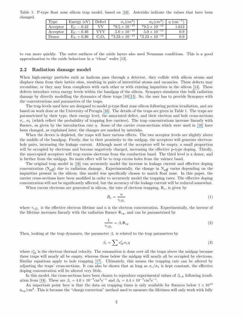
Table 1: P-type float zone silicon trap model, based on [16]. Asterisks indicate the values that have beenchanged.
Type Energy (eV) Defect σe(cm2) σh(cm2) η (cm−1)
Acceptor EC − 0.42 VV *9.5× 10−15 *9.5× 10−14 1.613Acceptor EC − 0.46 VVV 5.0 × 10⁻¹⁵ 5.0× 10⁻¹⁴ 0.9Donor EV + 0.36 CiOi *3.23× 10−13 *3.23× 10−14 0.9
to run more quickly. The outer surfaces of the oxide layers also used Neumann conditions. This is a goodapproximation to the oxide behaviour in a “clean” wafer [13].
2.2 Radiation damage model
When high-energy particles such as hadrons pass through a detector, they collide with silicon atoms anddisplace them from their lattice sites, resulting in pairs of interstitial atoms and vacancies. These defects mayrecombine, or they may form complexes with each other or with existing impurities in the silicon [14]. Thesedefects introduce extra energy levels within the bandgap of the silicon. Synopsys simulates this bulk radiationdamage by directly modelling the dynamics of these traps [10][15]. So, the user has to provide Synopsys withthe concentrations and parameters of the traps.
The trap levels used here are designed to model p-type float zone silicon following proton irradiation, and arebased on work done at the University of Perugia [16]. The details of the traps are given in Table 1. The traps areparametrised by their type, their energy level, the associated defect, and their electron and hole cross-sectionsσe, σh (which reflect the probability of trapping free carriers). The trap concentrations increase linearly withfluence, as given by the introduction rate η. Some of the carrier cross-sections which were used in [16] havebeen changed, as explained later; the changes are marked by asterisks.
When the device is depleted, the traps will have various effects. The two acceptor levels are slightly abovethe middle of the bandgap. Firstly, due to their proximity to the midgap, the acceptors will generate electron-hole pairs, increasing the leakage current. Although most of the acceptors will be empty, a small proportionwill be occupied by electrons and become negatively charged, increasing the effective p-type doping. Thirdly,the unoccupied acceptors will trap excess electrons from the conduction band. The third level is a donor, andis further from the midgap. Its main effect will be to trap excess holes from the valence band.
The original trap model in [16] can accurately model the increase in leakage current and effective dopingconcentration (Neff) due to radiation damage. Experimentally, the change in Neff varies depending on theimpurities present in the silicon; this model was specifically chosen to match float zone. In this paper, thecarrier cross-sections have been modified in order to accurately model the trapping rates. The effective dopingconcentration will not be significantly affected, but the accuracy of the leakage current will be reduced somewhat.
When excess electrons are generated in silicon, the rate of electron trapping, Re, is given by
Re =n
τeffe
(1)
where τeffeis the effective electron lifetime and n is the electron concentration. Experimentally, the inverse of
the lifetime increases linearly with the radiation fluence Φeq , and can be parametrised by
1
τeffe
= βeΦeq (2)
Then, looking at the trap dynamics, the parameter βe is related to the trap parameters by
βe =∑
vethσeη (3)
where veth is the electron thermal velocity. The summation is done over all the traps above the midgap because
these traps will nearly all be empty, whereas those below the midgap will nearly all be occupied by electrons.Similar equations apply to hole trapping [17]. Ultimately, this means the trapping rate can be altered byadjusting the traps’ cross-sections. It can also be shown that as long as σe/σh is kept constant, the effectivedoping concentration will be altered very little.
In this model, the cross-sections have been chosen to reproduce experimental values of βe,h following irradi-ation from [18]. These are βe = 4.0× 10⁻⁷cm2s−1 and βh = 4.4 × 10⁻⁷cm2s−1.
An important point here is that the data on trapping times is only available for fluences below 1 × 10¹⁵
neq/cm2. This is because the “charge correction” method used to measure the lifetimes will only work with fully
2
Figure 1: Comparison between simulated and experimental depletion voltages in n-in-p pad detectors. Experi-mental results are taken from [20].
depleted detectors, and at high fluences a detector’s depletion voltage becomes very large. So, this model workson the assumption that the linear relationship between fluence and trapping in equation (2) can be extrapolated
all the way up to 1 × 10¹⁶ neq/cm2.Since the behaviour of the traps is affected by the width of the bandgap, all the simulations were done using
the same bandgap model—Slotboom [19]. These trap models were designed to work using Synopsys TCAD’sdefault temperature setting of 300K, whereas during lab tests a detector may operate at “room temperature”or be cooled to 263K or so depending on the particular test setup. (When they are not being tested, detectorsare stored at low temperatures to prevent unwanted annealing.) Experimentally, the leakage current generatedby the traps increases predictably with temperature, and leakage current values are normally scaled to 293K toallow a fair comparison [7].
Finally, to model the effects of surface damage, a layer of uniform positive charge was introduced at theinterface between the silicon substrate and the oxide layer. This had an area density of 4 × 1011cm−2 beforeirradiation, and 1 × 1012cm−2 after irradiation [16].
2.3 Comparing the damage model to experiment
Next, this radiation damage model was applied to planar detectors, to check that it gives accurate results.Firstly, a 280µm-thick n-in-p pad detector was simulated with different damage fluences, to determine thevariation in depletion voltage and leakage current. The structure and substrate doping of these devices matchedthose tested in [20]. The resulting depletion voltages in Fig. 1 show a good match between the simulation andexperiment.
The leakage current after irradiation is parametrised by Ileak/Vol = αΦeq . The simulation gives α =5.13 × 10⁻¹⁷Acm−1, whereas the experimental value is α = (3.99 ± 0.03) × 10−17Acm−1, measured at 293Kfollowing an 80 minute anneal at 60◦C [21]. So, the simulated value is about 30% higher than experiment.Given that these simulations are intended to model Neff and trapping rather than leakage current, and theexperimental value of the leakage current can change by more than 30% under different annealing conditions,this result is acceptable.
Next, the charge collection behaviour of a 280µm-thick n-in-p strip detector detector was simulated. Thiswas done by starting a simulation with charge deposited along a track passing through the full thickness of thedetector. The track generated 80 electron-hole pairs per micrometre, which is the most probable energy lossfor a minimum ionising particle (MIP) passing through silicon, and its lateral profile was Gaussian with 1µmstandard deviation. The device’s behaviour was simulated over time, and the current at the readout electrodewas integrated over 10ns, after subtracting the leakage current, to find the total charge collected. The simulationconditions were chosen to match the tests done in [22]—in particular, all the simulations were done at a highbias of 900V.
3
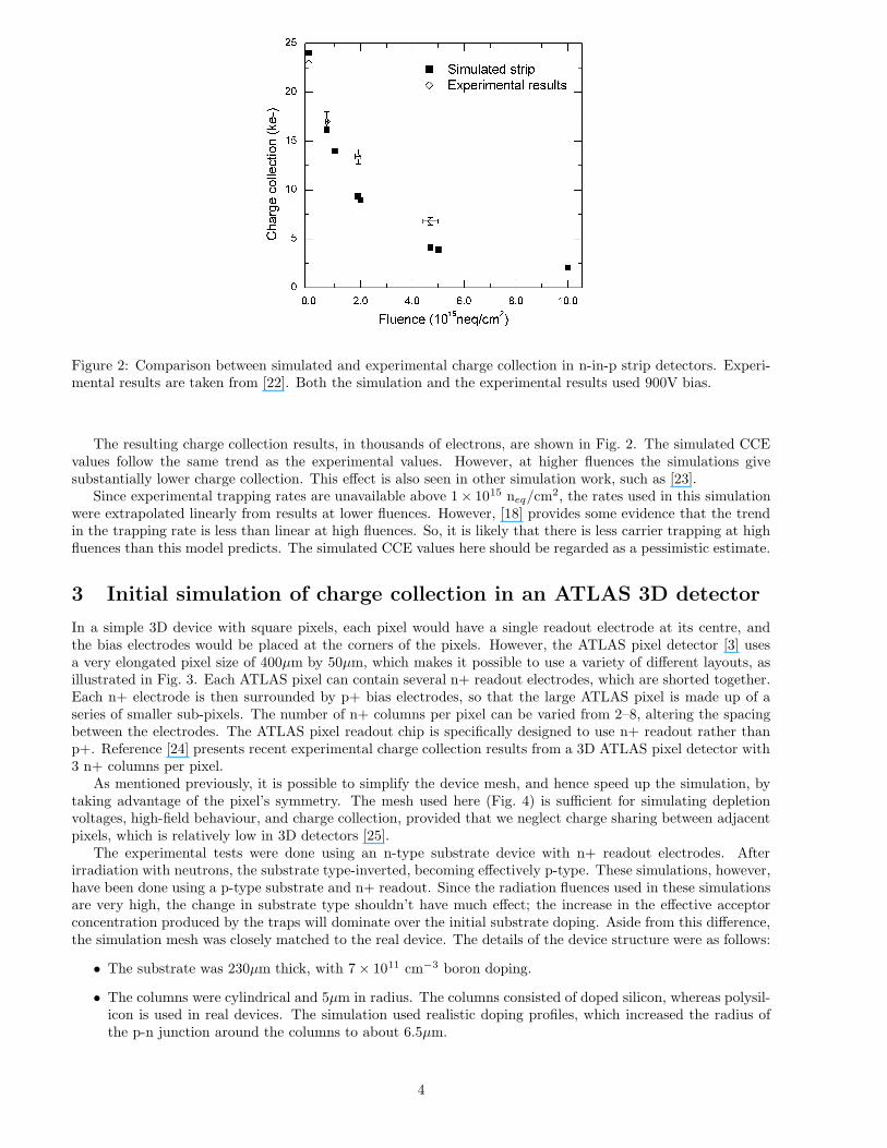
Figure 2: Comparison between simulated and experimental charge collection in n-in-p strip detectors. Experi-mental results are taken from [22]. Both the simulation and the experimental results used 900V bias.
The resulting charge collection results, in thousands of electrons, are shown in Fig. 2. The simulated CCEvalues follow the same trend as the experimental values. However, at higher fluences the simulations givesubstantially lower charge collection. This effect is also seen in other simulation work, such as [23].
Since experimental trapping rates are unavailable above 1× 10¹⁵ neq/cm2, the rates used in this simulationwere extrapolated linearly from results at lower fluences. However, [18] provides some evidence that the trendin the trapping rate is less than linear at high fluences. So, it is likely that there is less carrier trapping at highfluences than this model predicts. The simulated CCE values here should be regarded as a pessimistic estimate.
3 Initial simulation of charge collection in an ATLAS 3D detector
In a simple 3D device with square pixels, each pixel would have a single readout electrode at its centre, andthe bias electrodes would be placed at the corners of the pixels. However, the ATLAS pixel detector [3] usesa very elongated pixel size of 400µm by 50µm, which makes it possible to use a variety of different layouts, asillustrated in Fig. 3. Each ATLAS pixel can contain several n+ readout electrodes, which are shorted together.Each n+ electrode is then surrounded by p+ bias electrodes, so that the large ATLAS pixel is made up of aseries of smaller sub-pixels. The number of n+ columns per pixel can be varied from 2–8, altering the spacingbetween the electrodes. The ATLAS pixel readout chip is specifically designed to use n+ readout rather thanp+. Reference [24] presents recent experimental charge collection results from a 3D ATLAS pixel detector with3 n+ columns per pixel.
As mentioned previously, it is possible to simplify the device mesh, and hence speed up the simulation, bytaking advantage of the pixel’s symmetry. The mesh used here (Fig. 4) is sufficient for simulating depletionvoltages, high-field behaviour, and charge collection, provided that we neglect charge sharing between adjacentpixels, which is relatively low in 3D detectors [25].
The experimental tests were done using an n-type substrate device with n+ readout electrodes. Afterirradiation with neutrons, the substrate type-inverted, becoming effectively p-type. These simulations, however,have been done using a p-type substrate and n+ readout. Since the radiation fluences used in these simulationsare very high, the change in substrate type shouldn’t have much effect; the increase in the effective acceptorconcentration produced by the traps will dominate over the initial substrate doping. Aside from this difference,the simulation mesh was closely matched to the real device. The details of the device structure were as follows:
• The substrate was 230µm thick, with 7 × 1011 cm−3 boron doping.
• The columns were cylindrical and 5µm in radius. The columns consisted of doped silicon, whereas polysil-icon is used in real devices. The simulation used realistic doping profiles, which increased the radius ofthe p-n junction around the columns to about 6.5µm.
4
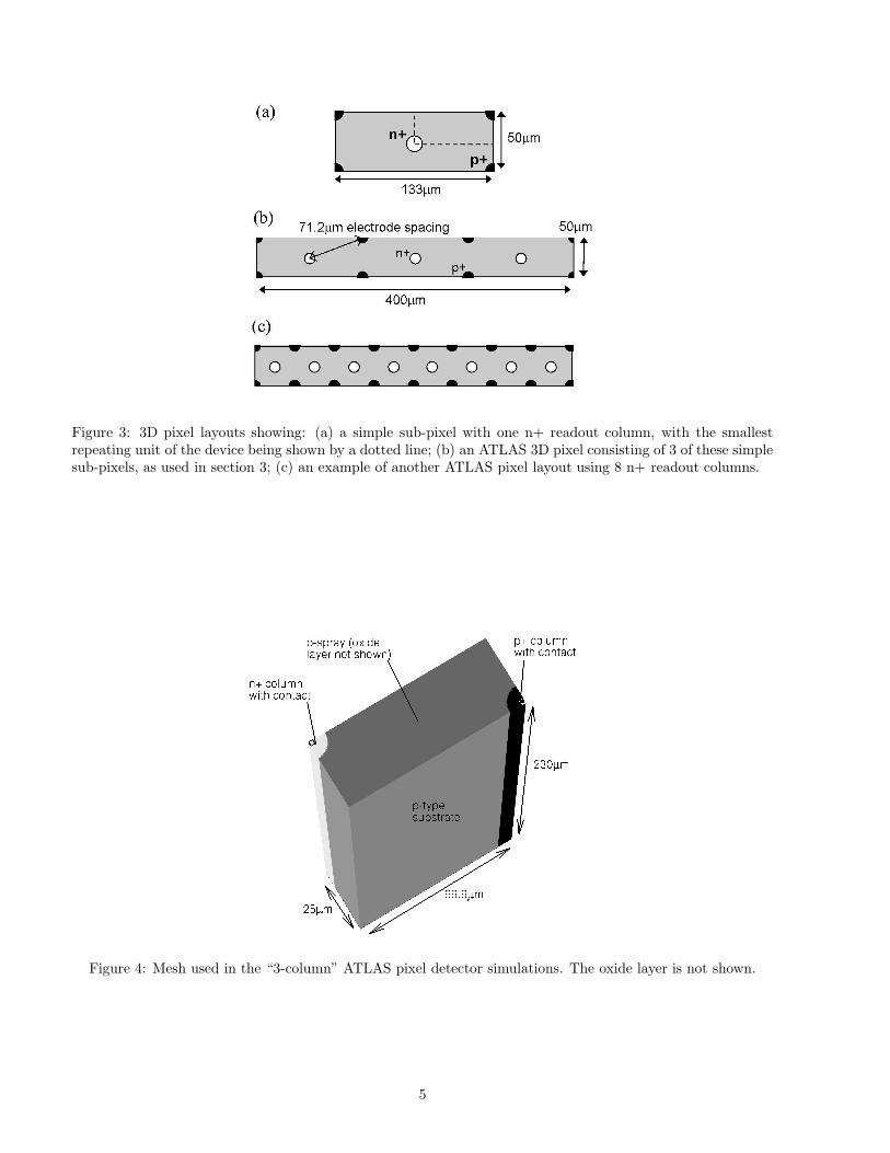
Figure 3: 3D pixel layouts showing: (a) a simple sub-pixel with one n+ readout column, with the smallestrepeating unit of the device being shown by a dotted line; (b) an ATLAS 3D pixel consisting of 3 of these simplesub-pixels, as used in section 3; (c) an example of another ATLAS pixel layout using 8 n+ readout columns.
Figure 4: Mesh used in the “3-column” ATLAS pixel detector simulations. The oxide layer is not shown.
5

Figure 5: Comparison between simulated and experimental charge collection in a “3-column” ATLAS pixeldetector. Experimental results are taken from [24]. The labels indicate the bias used in both the experimentsand the simulations.
• The n+ columns were isolated using a p-spray [26] covering the front and back surfaces. This used atotal boron dose of 1.2 × 1012 cm−2, and had a peak concentration of 2.5 × 1016 cm−3. The p-spray waschosen to have a high enough dose to compensate for the electron layer (preventing it from linking then+ columns together) and to have a fairly realistic profile.
This mesh was then used to do a series of charge collection simulations. The experimental tests [24] had beendone using a de-focused, pulsed 1060nm IR laser, which should provide fairly uniform charge deposition withdepth. The resulting charge collection was then scaled to find the corresponding signal that would be producedby a minimum ionizing particle, which generates 80 electron-hole pairs per micrometre of silicon. In the test,a large number of pixels were connected together, which means charge sharing would have had no effect, andthe current signals measured were averaged over 1000 pulses. To give an equivalent test of the average chargecollection, the following simulations used uniform charge deposition throughout the device. Once again, thecharge density was chosen to match a minimum ionising particle, giving a total of about 18500 electron-holepairs. As before, the current signal was integrated over 10ns, after correcting for the leakage current. Lastly,since the experimental tests were done using different biases at different fluences, the simulations also usedvarying biases. The charge collection results are shown in Fig. 5, and each data point is labelled with thecorresponding bias voltage.
Once again, the simulation results show a similar trend to the experimental results, but give lower chargecollection. The likely reasons for this have been discussed in section 2.3. In the planar detector simulation (Fig.2) the simulated collection efficiencies at high fluence are about 60%–70% of the experimental values, and thesame is true for the 3D detector, even though the two devices have very different structures. This indicates thatthese simulations can be useful for comparing and understanding the behaviour of different device structures.
4 Comprehensive simulation of 3D ATLAS pixel devices at 1016neq/cm
2
fluence
As mentioned in section 3, a variety of different 3D ATLAS pixel layouts are possible, with the number ofn+ electrodes per pixel ranging from 2 to 8—see Fig. 3 for examples of 3- and 8-column layouts. Using thesame methods as described in the previous sections, all of these device layouts have been simulated in order tocompare their performance at high fluence.
6
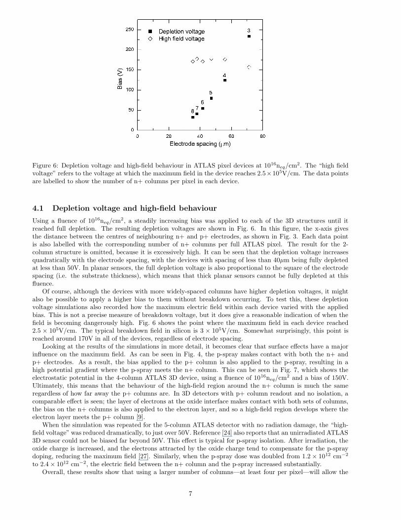
Figure 6: Depletion voltage and high-field behaviour in ATLAS pixel devices at 1016neq/cm2. The “high fieldvoltage” refers to the voltage at which the maximum field in the device reaches 2.5×10⁵V/cm. The data pointsare labelled to show the number of n+ columns per pixel in each device.
4.1 Depletion voltage and high-field behaviour
Using a fluence of 1016neq/cm2, a steadily increasing bias was applied to each of the 3D structures until itreached full depletion. The resulting depletion voltages are shown in Fig. 6. In this figure, the x-axis givesthe distance between the centres of neighbouring n+ and p+ electrodes, as shown in Fig. 3. Each data pointis also labelled with the corresponding number of n+ columns per full ATLAS pixel. The result for the 2-column structure is omitted, because it is excessively high. It can be seen that the depletion voltage increasesquadratically with the electrode spacing, with the devices with spacing of less than 40µm being fully depletedat less than 50V. In planar sensors, the full depletion voltage is also proportional to the square of the electrodespacing (i.e. the substrate thickness), which means that thick planar sensors cannot be fully depleted at thisfluence.
Of course, although the devices with more widely-spaced columns have higher depletion voltages, it mightalso be possible to apply a higher bias to them without breakdown occurring. To test this, these depletionvoltage simulations also recorded how the maximum electric field within each device varied with the appliedbias. This is not a precise measure of breakdown voltage, but it does give a reasonable indication of when thefield is becoming dangerously high. Fig. 6 shows the point where the maximum field in each device reached2.5 × 105V/cm. The typical breakdown field in silicon is 3 × 10⁵V/cm. Somewhat surprisingly, this point isreached around 170V in all of the devices, regardless of electrode spacing.
Looking at the results of the simulations in more detail, it becomes clear that surface effects have a majorinfluence on the maximum field. As can be seen in Fig. 4, the p-spray makes contact with both the n+ andp+ electrodes. As a result, the bias applied to the p+ column is also applied to the p-spray, resulting in ahigh potential gradient where the p-spray meets the n+ column. This can be seen in Fig. 7, which shows theelectrostatic potential in the 4-column ATLAS 3D device, using a fluence of 1016neq/cm2 and a bias of 150V.Ultimately, this means that the behaviour of the high-field region around the n+ column is much the sameregardless of how far away the p+ columns are. In 3D detectors with p+ column readout and no isolation, acomparable effect is seen; the layer of electrons at the oxide interface makes contact with both sets of columns,the bias on the n+ columns is also applied to the electron layer, and so a high-field region develops where theelectron layer meets the p+ column [9].
When the simulation was repeated for the 5-column ATLAS detector with no radiation damage, the “high-field voltage” was reduced dramatically, to just over 50V. Reference [24] also reports that an unirradiated ATLAS3D sensor could not be biased far beyond 50V. This effect is typical for p-spray isolation. After irradiation, theoxide charge is increased, and the electrons attracted by the oxide charge tend to compensate for the p-spraydoping, reducing the maximum field [27]. Similarly, when the p-spray dose was doubled from 1.2 × 1012 cm−2
to 2.4 × 1012 cm−2, the electric field between the n+ column and the p-spray increased substantially.Overall, these results show that using a larger number of columns—at least four per pixel—will allow the
7
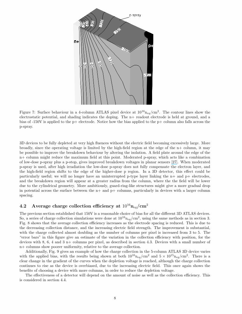
Figure 7: Surface behaviour in a 4-column ATLAS pixel device at 1016neq/cm2. The contour lines show theelectrostatic potential, and shading indicates the doping. The n+ readout electrode is held at ground, and abias of -150V is applied to the p+ electrode. Notice how the bias applied to the p+ column also falls across thep-spray.
3D devices to be fully depleted at very high fluences without the electric field becoming excessively large. Morebroadly, since the operating voltage is limited by the high-field region at the edge of the n+ column, it maybe possible to improve the breakdown behaviour by altering the isolation. A field plate around the edge of then+ column might reduce the maximum field at this point. Moderated p-spray, which acts like a combinationof low-dose p-spray plus a p-stop, gives improved breakdown voltages in planar sensors [27]. When moderatedp-spray is used, after high irradiation the low-dose p-spray does not fully compensate the electron layer, andthe high-field region shifts to the edge of the higher-dose p region. In a 3D detector, this effect could beparticularly useful; we will no longer have an uninterrupted p-type layer linking the n+ and p+ electrodes,and the breakdown region will appear at a greater radius from the column, where the the field will be lowerdue to the cylindrical geometry. More ambitiously, guard-ring-like structures might give a more gradual dropin potential across the surface between the n+ and p+ columns, particularly in devices with a larger columnspacing.
4.2 Average charge collection efficiency at 1016neq/cm
2
The previous section established that 150V is a reasonable choice of bias for all the different 3D ATLAS devices.So, a series of charge collection simulations were done at 1016neq/cm2, using the same methods as in section 3.Fig. 8 shows that the average collection efficiency increases as the electrode spacing is reduced. This is due tothe decreasing collection distance, and the increasing electric field strength. The improvement is substantial,with the charge collected almost doubling as the number of columns per pixel is increased from 3 to 5. The“error bars” in this figure give an estimate of the variation in the collection efficiency with position, for thedevices with 8, 6, 4 and 3 n+ columns per pixel, as described in section 4.3. Devices with a small number ofn+ columns show poorer uniformity, relative to the average collection.
Additionally, Fig. 9 gives an example of how the charge collection in the 5-column ATLAS 3D device varieswith the applied bias, with the results being shown at both 1016neq/cm2 and 5 × 10¹⁵neq/cm2. There is aclear change in the gradient of the curves when the depletion voltage is reached, although the charge collectioncontinues to rise as the device is overbiased, due to the increasing electric field. This once again shows thebenefits of choosing a device with more columns, in order to reduce the depletion voltage.
The effectiveness of a detector will depend on the amount of noise as well as the collection efficiency. Thisis considered in section 4.4.
8
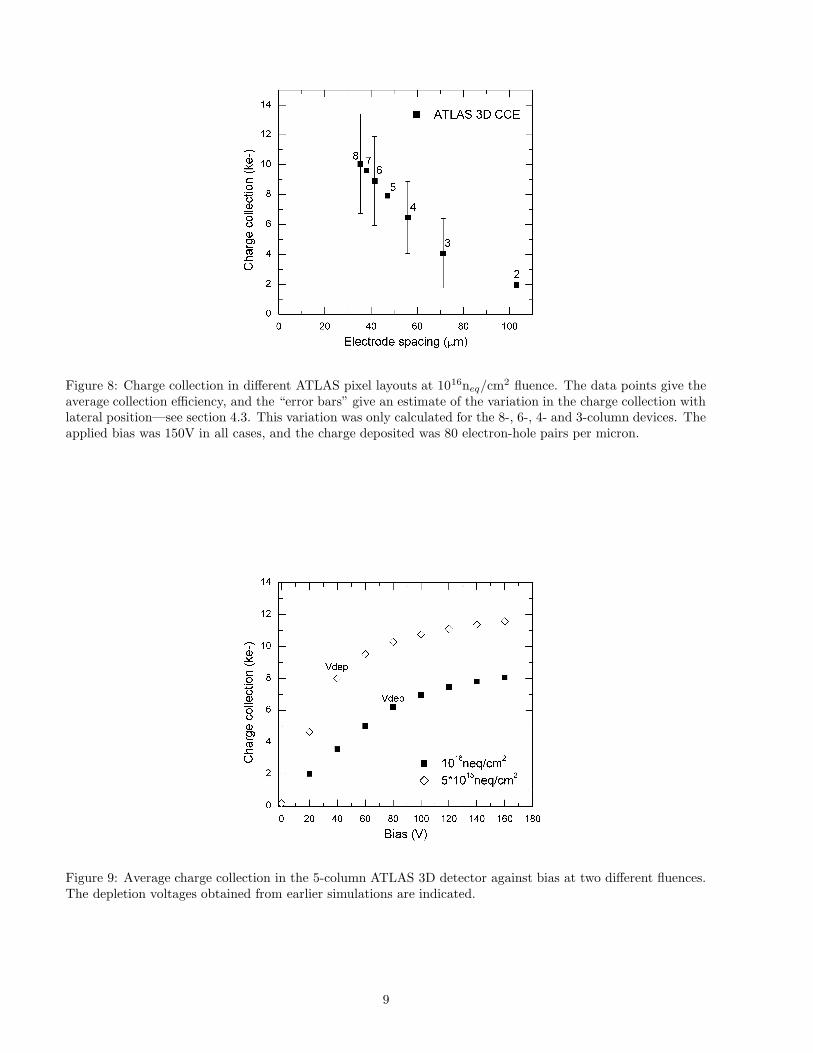
Figure 8: Charge collection in different ATLAS pixel layouts at 1016neq/cm2 fluence. The data points give theaverage collection efficiency, and the “error bars” give an estimate of the variation in the charge collection withlateral position—see section 4.3. This variation was only calculated for the 8-, 6-, 4- and 3-column devices. Theapplied bias was 150V in all cases, and the charge deposited was 80 electron-hole pairs per micron.
Figure 9: Average charge collection in the 5-column ATLAS 3D detector against bias at two different fluences.The depletion voltages obtained from earlier simulations are indicated.
9

4.3 Uniformity of the charge collection across the pixel
Using a 3D detector structure means that the electric field and the carrier drift distances vary with the horizontalposition across each pixel, rather than with depth. As a result, the charge collection efficiency may vary withhorizontal position, too. The significance of this effect will vary depending on how the detector is used; if allthe tracks are travelling parallel to the electrode columns, the effect will be particularly important.
Firstly, there is the effect of the electrode columns themselves. As shown in [28], the collection efficiency issubstantially reduced within the columns, due to the lack of an electric field. As the number of columns percell increases, the total area they occupy will obviously increase. The columns in these simulations are 5µmin radius, with a doping profile extending a further 1.5µm, which is the smallest radius that can currently beachieved with 250µm columns. With these conditions, the columns will occupy 5% of the device volume in the4-electrode device, and 10% if 8 n+ electrodes per pixel are used. If the radius of the columns is increasedby just 2µm, their total area will be doubled. Furthermore, unlike some of the other effects (e.g. trapping,increasing Neff), the column area will reduce the device’s effectiveness even before irradiation. So, although theaverage collected signal at 1016neq/cm2 steadily increases as more columns are used, it may be better to use adevice with a lower average CCE and a smaller column area.
Secondly, Fig. 10 shows the electric field distributions in the 6-, 4- and 3-column ATLAS 3D devices, takenfrom horizontal cross-sections. Once again, the safe operating voltage of 150V was used. All the devices showweaker electric fields towards the null points which occur at the “corners” of the mesh, midway between then+ columns in neighbouring subpixels. Additionally, as the electrode spacing increases, the field becomes lessuniform along the length of the pixel; in the 4-column device the field is distinctly weaker towards the p+column, and the 3-column device is not fully depleted around the p+. This effect is due to the increase in thefull depletion voltage.
The variation in the collection efficiency was studied by simulating the effects of minimum ionising particlespassing through the detectors in different places. Because this was time-consuming to simulate, only the 8, 6,4 and 3-column devices were considered. Each minimum ionising particle passed vertically through the device,generating 80e-h pairs/µm. The tracks had a Gaussian lateral distribution, with a standard deviation of 1µm.These MIPs were simulated at 25 different positions in each detector structure, forming a regularly-spaced 5×5rectangular grid. Looking at the X and Y axes in Fig. 10, the first MIP was deposited at (2.5µm, 2.5µm),falling within the n+ column, and the final MIP deposited at the equivalent position within the p+ column. Asbefore, these simulations were done at 1016neq/cm2, with 150V bias. Note that this simulation didn’t considerthe effects of charge sharing at the very edges of each pixel.
For each structure, the charge collection values from the 25 MIPs were averaged. These average valueswere close to the results obtained earlier in section 4.2, with the biggest difference being 6%. So, this showsthat while the 5 × 5 pattern doesn’t map the collection efficiency with great resolution, the results are stillreasonably representative of each device’s behaviour. Next, the standard deviation of each set of MIP resultswas calculated, as a measure of the variation in collection efficiency with position. The standard deviation isshown in Fig.8 by the “error bars”. Relative to the average CCE, the standard deviation is larger in the deviceswith fewer n+ columns.
Fig. 11 shows the charge collection with position for the 4-column ATLAS 3D detector as an example. Inall of these ATLAS devices, negligible charge is collected when the MIP falls within the n+ or p+ column,as expected. (This confirms that the average collection simulated earlier includes the effects of the columns.)Aside from the columns, the lowest collection efficiencies are seen around the null points, as mentioned earlier,and to some extent around the edges of the cell - particularly the short edges in the devices with fewer columns.Generally, the highest collection signals are seen somewhere midway between the n+ and p+ columns. In mostof the devices, the collection behaviour is somewhat more uniform than the electric field itself—for example,the 4-column device has a distinctly lower field near the p+ column than near the n+ (Fig. 10b) but there isn’tas much difference in the collected signal from these two regions (Fig. 11). However, the 3-column device showsvery poor collection around the p+ column, because this region isn’t fully depleted.
4.4 Capacitance and noise
Next, the capacitances of the ATLAS 3D structures were simulated. While the previous simulations used arelatively small region of the device, so that the charge collection simulations would be faster, the capacitancesimulations were done using larger meshes. This meant that the C-V simulations were able to find the capaci-tance between the n+ readout columns and the p+ bias columns, and also the inter-pixel capacitance betweenone set of n+ columns and those in the two neighbouring pixels. Because ATLAS pixels are so elongated, theinterpixel capacitance is much greater between pixels sharing their 400µm-long sides than those sharing their50µm-long sides. The simulation does not account for the effects of the n+ and p+ columns in further-awaypixels, but these effects should be fairly small. These capacitance simulations were done using saturated surface
10
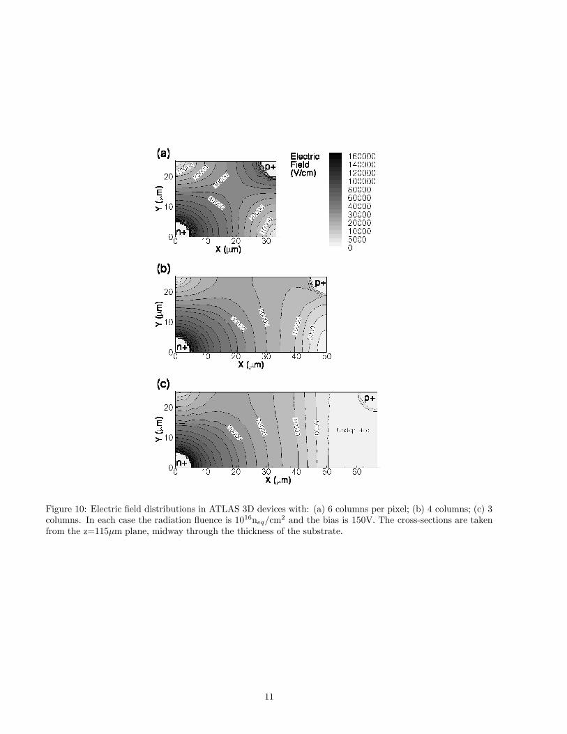
Figure 10: Electric field distributions in ATLAS 3D devices with: (a) 6 columns per pixel; (b) 4 columns; (c) 3columns. In each case the radiation fluence is 1016neq/cm2 and the bias is 150V. The cross-sections are takenfrom the z=115µm plane, midway through the thickness of the substrate.
11
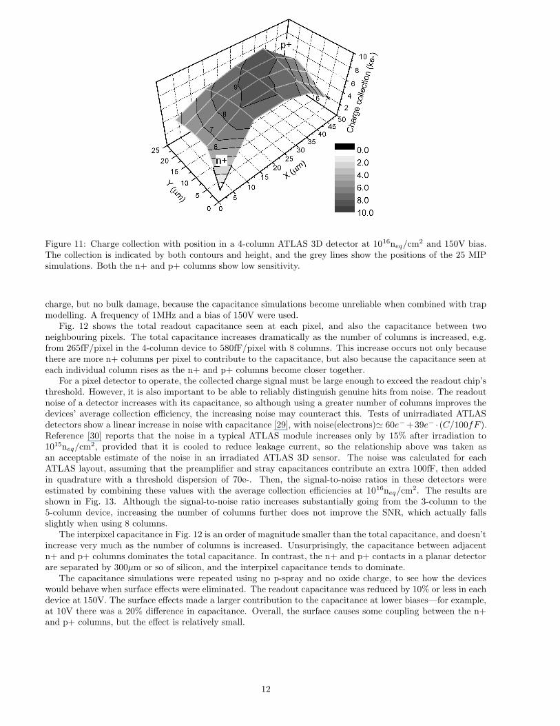
Figure 11: Charge collection with position in a 4-column ATLAS 3D detector at 1016neq/cm2 and 150V bias.The collection is indicated by both contours and height, and the grey lines show the positions of the 25 MIPsimulations. Both the n+ and p+ columns show low sensitivity.
charge, but no bulk damage, because the capacitance simulations become unreliable when combined with trapmodelling. A frequency of 1MHz and a bias of 150V were used.
Fig. 12 shows the total readout capacitance seen at each pixel, and also the capacitance between twoneighbouring pixels. The total capacitance increases dramatically as the number of columns is increased, e.g.from 265fF/pixel in the 4-column device to 580fF/pixel with 8 columns. This increase occurs not only becausethere are more n+ columns per pixel to contribute to the capacitance, but also because the capacitance seen ateach individual column rises as the n+ and p+ columns become closer together.
For a pixel detector to operate, the collected charge signal must be large enough to exceed the readout chip’sthreshold. However, it is also important to be able to reliably distinguish genuine hits from noise. The readoutnoise of a detector increases with its capacitance, so although using a greater number of columns improves thedevices’ average collection efficiency, the increasing noise may counteract this. Tests of unirradiated ATLASdetectors show a linear increase in noise with capacitance [29], with noise(electrons)' 60e−+39e− · (C/100fF ).Reference [30] reports that the noise in a typical ATLAS module increases only by 15% after irradiation to1015neq/cm2, provided that it is cooled to reduce leakage current, so the relationship above was taken asan acceptable estimate of the noise in an irradiated ATLAS 3D sensor. The noise was calculated for eachATLAS layout, assuming that the preamplifier and stray capacitances contribute an extra 100fF, then addedin quadrature with a threshold dispersion of 70e-. Then, the signal-to-noise ratios in these detectors wereestimated by combining these values with the average collection efficiencies at 1016neq/cm2. The results areshown in Fig. 13. Although the signal-to-noise ratio increases substantially going from the 3-column to the5-column device, increasing the number of columns further does not improve the SNR, which actually fallsslightly when using 8 columns.
The interpixel capacitance in Fig. 12 is an order of magnitude smaller than the total capacitance, and doesn’tincrease very much as the number of columns is increased. Unsurprisingly, the capacitance between adjacentn+ and p+ columns dominates the total capacitance. In contrast, the n+ and p+ contacts in a planar detectorare separated by 300µm or so of silicon, and the interpixel capacitance tends to dominate.
The capacitance simulations were repeated using no p-spray and no oxide charge, to see how the deviceswould behave when surface effects were eliminated. The readout capacitance was reduced by 10% or less in eachdevice at 150V. The surface effects made a larger contribution to the capacitance at lower biases—for example,at 10V there was a 20% difference in capacitance. Overall, the surface causes some coupling between the n+and p+ columns, but the effect is relatively small.
12
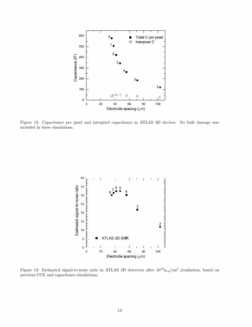
Figure 12: Capacitance per pixel and interpixel capacitance in ATLAS 3D devices. No bulk damage wasincluded in these simulations.
Figure 13: Estimated signal-to-noise ratio in ATLAS 3D detectors after 1016neq/cm2 irradiation, based onprevious CCE and capacitance simulations.
13
5 Conclusions
These simulations have modelled the behaviour of different 3D detectors at Super-LHC radiation damage levels.Overall, the simulations show improved depletion and charge collection behaviour compared to planar detectors.Comparisons between different ATLAS 3D pixel layouts have shown that if the number of n+ electrodes perpixel is small, the wide electrode spacing means that the depletion voltage, the average collection efficiency andthe uniformity of the collection across the pixel are poorer. The surface effects which can cause breakdownare not strongly affected by the electrode spacing. Getting an acceptable depletion voltage and uniformity athigh fluence requires at least 4 columns per pixel. Conversely, using a large number of columns per pixel willmean that the columns themselves will take up a significant proportion of the device volume (particularly ifthe columns have a greater radius than the 5µm used here), and the rapidly increasing capacitive noise limitsthe signal-to-noise ratio. The improvements in the absolute charge collection and depletion voltage obtained byusing more than 6 columns are relatively small. So, for detectors operating at 1016neq/cm2, the best trade-offis likely to be achieved by using 4-6 columns.
Currently, groups within the CERN RD50 collaboration and the ATLAS 3D sensors project are producinga variety of 3D devices. These simulations should complement these experimental tests, by highlighting po-tential problems with the devices such as high capacitance or nonuniformity in collection, and by aiding theunderstanding of these devices’ behaviour.
References
[1] J. Ellis, Physics at the LHC, European Physical Journal C 34 (1) (2004) 51–56.
[2] F. Gianotti, Physics opportunities of the LHC luminosity upgrade, Nuclear Physics B-Proceedings Supple-ments 147 (2005) 23–32.
[3] G. Gagliardi, The ATLAS pixel detector: A hundred million channels vertex detector for LHC, Nucl. Instr.and Meth A 546 (1-2) (2005) 67–71.
[4] Y. Unno, Silicon sensor development for the ATLAS upgrade for SLHC, Nucl. Instr. and Meth A 569 (1)(2006) 41–47.
[5] S. I. Parker, C. J. Kenney, J. Segal, 3D - a proposed new architecture for solid-state radiation detectors,Nucl. Instr. and Meth A 395 (3) (1997) 328–343.
[6] C. Da Via, G. Anelli, J. Hasi, P. Jarron, C. Kenney, A. Kok, S. Parker, E. Perozziello, S. J. Watts,Advances in silicon detectors for particle tracking in extreme radiation environments, Nucl. Instr. andMeth A 509 (1-3) (2003) 86–91.
[7] M. Moll on behalf of the RD50 collaboration, Radiation tolerant semiconductor sensors for tracking detec-tors, Nucl. Instr. and Meth A 565 (1) (2006) 202–211.
[8] J. Kalliopuska, S. Eranen, R. Orava, Charge collection characterization of a 3D silicon radiation detectorby using 3D simulations, Nucl. Instr. and Meth A 572 (1) (2007) 292–296.
[9] D. Pennicard, G. Pellegrini, M. Lozano, R. Bates, C. Parkes, V. O’Shea, V. Wright, Simulation resultsfrom double-sided 3D detectors, IEEE Trans. Nucl. Sci. 54 (4) (2007) 1435–1443.
[10] Synopsys Inc., Synopsys TCAD manuals, http://www.synopsys.com/products/tcad/tcad.html, (2007).
[11] G. Lutz, Semiconductor Radiation Detectors Device Physics, 1st Edition, Springer-Verlag, Berlin Heidel-berg New York, 1999.
[12] J. Kalliopuska, S. Eranen, R. Orava, 3D simulations of 3D silicon radiation detector structures, Nucl. Instr.and Meth A 568 (1) (2006) 27–33.
[13] R. H. Richter, L. Andricek, T. Gebhart, D. Hauff, J. Kemmer, G. Lutz, R. Weiss, A. Rolf, Strip detectordesign for ATLAS and HERA-B using two-dimensional device simulation, Nucl. Instr. and Meth A 377 (2-3)(1996) 412–421.
[14] V. Eremin, E. Verbitskaya, Z. Li, Effect of radiation induced deep level traps on Si detector performance,Nucl. Instr. and Meth A 476 (3) (2002) 537–549.
14
[15] W. Shockley, W. T. Read, Statistics of the recombinations of holes and electrons, Physical Review 87 (5)(1952) 835–842.
[16] M. Petasecca, F. Moscatelli, D. Passeri, G. U. Pignatel, Numerical simulation of radiation damage effectsin p-type and n-type FZ silicon detectors, IEEE Trans. Nucl. Sci. 53 (5) (2006) 2971–2976.
[17] G. Kramberger, V. Cindro, I. Mandic, M. Mikuz, M. Zavrtanik, Effective trapping time of electrons andholes in different silicon materials irradiated with neutrons, protons and pions, Nucl. Instr. and Meth A481 (1-3) (2002) 297–305.
[18] V. Cindro, G. Kramberger, M. Lozano, I. Mandic, M. Mikuz, G. Pellegrini, J. Pulko, M. Ullan, M. Za-vrtanik, Trapping of electrons and holes in p-type silicon irradiated with neutrons, IEEE Nuclear ScienceSymposium Conference Record 1 (2006) 139–142.
[19] J. W. Slotboom, H. C. Degraaff, Measurements of bandgap narrowing in Si bipolar-transistors, Solid-StateElectronics 19 (10) (1976) 857–862.
[20] M. Lozano, G. Pellegrini, C. Fleta, C. Loderer, J. M. Rafi, M. Ullan, F. Campabadal, C. Martinez, M. Key,G. Casse, P. Allport, Comparison of radiation hardness of p-in-n, n-in-n, and n-in-p silicon pad detectors,IEEE Trans. Nucl. Sci. 52 (5) (2005) 1468–1473.
[21] M. Moll, Radiation damage in silicon particle detectors - microscopic defects and macroscopic properties,Thesis/dissertation, Hamburg (1999).
[22] P. P. Allport, G. Casse, M. Lozano, P. Sutcliffe, J. J. Velthuis, J. Vossebeld, Performance of p-type micro-strip detectors after irradiation to 7.5 x 10¹⁵ p/cm2, IEEE Trans. Nucl. Sci. 52 (5) (2005) 1903–1906.
[23] G. Kramberger, V. Cindro, I. Mandic, M. Mikuz, Impact of annealing of trapping times on charge collectionin irradiated silicon detectors, Nucl. Instr. and Meth A 579 (2) (2007) 762–765.
[24] C. Da Via, J. Hasi, C. Kenney, V. Linhart, S. Parker, T. Slavicek, S.J.Watts, P. Bem, T. Horadzofski andS. Pospisil, Radiation hardness properties of full-3D active edge silicon sensors, Nucl. Instr. and Meth A587 (2-3) (2008) 243–249.
[25] V. A. Wright, W. D. Davidson, J. J. Melone, V. O’Shea, K. M. Smith, L. Donohue, L. Lea, K. Robb,S. Nenonen, H. Sipila, Three-dimensional Medipix - a new generation of X-ray detectors, IEEE Trans.Nucl. Sci. 52 (5) (2005) 1873–1876.
[26] G. Pellegrini, C. Fleta, F. Campabadal, S. Diez, M. Lozano, J. M. Rafi, M. Ullan, Technology developmentof p-type microstrip detectors with radiation hard p-spray isolation, Nucl. Instr. and Meth A 566 (2) (2006)360–365.
[27] C. Piemonte, Device simulations of isolation techniques for silicon microstrip detectors made on p-typesubstrates, IEEE Trans. Nucl. Sci. 53 (3) (2006) 1694–1705.
[28] A. Kok, Signal formation and active edge studies of 3D silicon detector technology, Thesis/dissertation,Brunel University (2005).
[29] A. Andreazza, Progresses on the ATLAS pixel detector, Nucl. Instr. and Meth A 461 (1-3) (2001) 168–171.
[30] J. Grosse-Knetter, The ATLAS pixel detector, Nucl. Instr. and Meth A 568 (1) (2006) 252–257.
15