Astrophysical Parameter Determination Using Chaotic Orbital ...
Upload
independentCategory
view
6download
0
Simulation and Implementation of Improved Chaotic Colpitts Circuit for UWB Communications
Nguyen Xuan Quyen, Bui Tran Quyet, Vu Van Vern, Nguyen Tien Dzung and Thang Manh Hoang Faculty of Electronics and Telecommunications
Hanoi University of Science and Technology 1 Dai Co Viet Road, Hai Ba Trung District, Hanoi, VIETNAM
Tel: +84438692242; Fax: +84438692241 Email: [email protected]
Abstract - In this paper, we develop an improved chaotic Colpitts oscillator applied to ultra wide band wireless communication system. We design, simulate and implement the improved chaotic Colpitts oscillator using Philip's wideband transistor BJT BFG425W. The numerical simulation using Matlab and circuit simulation using Advanced Design System (ADS) are also presented. The oscillator is designed based on micro-strip substrate and the simulation result of the layout approves the possibility for UWB wireless communication applications.
Keywords - Improved chaotic Colpitts oscillator; Wide band; chaos; non-linear dynamic.
I. INTRODUCTION
Chaos-based communications have been received a lot of attention of researchers since the discovery of property of selfsynchronization of chaotic systems by Pecora and Carroll [1]. Chaotic signals have suitable characteristics for communications such as its ultra wide bandwidth, its stability to fading in multipath environment, its relative simply circuit as well as its possibility of control and synchronization, etc. These advantages promote the study of applying chaotic signal to modem wideband wireless communication systems.
II. IMPROVED CHAOTIC COLPITTS OSCILLATOR
The configuration of an improved chaotic oscillator and a standard version are shown in the Fig.I . We can see that they consist of a BJT as the gain element and a resonant network including an inductor and a pair of capacitors. The difference between conventional Colpitts oscillator and the improved version is that the inductor L is moved from the collector to the base of transistor where it is in series with resistor Rb.
The basic mechanism behind the improved configuration version is the diminishing of negative influence of capacitor CcB (zero-bias collector-base capacitance). In the standard version of Colpitts oscillator, capacitor CCB grounds the collector node and acts as a parasitic element destroying chaotic oscillations. In this novel version, L and Rb screen CCB from ground and reduce its negative influence.
The state equations for the improved chaotic Colpitts oscillator depicted in the Fig.1 are as:
dVCl RCI--= Vo -VCI -VC2 +RIL -R(fJ+I)IB
dt
dVC2 RC2 --= Vo -VCI -VC2 -RIo +RIL
dt
dIL L-=-RbIL -VBE -VC2
dt
(I) After the first report of chaotic phenomenon in the Colpitts
oscillator [2], lots of researchers have made great contributions to the design of this circuit with higher frequency band. It was investigated at the low frequencies (kHz), high frequencies (3-300 MHz) and ultra-high frequencies (300-1000 MHz) [3-6]. However, it is analyzed that the highest achievable value of the fundamental frequency f* in chaotic Colpitts oscillator is about O.lfT where fT is the threshold frequency of the employed transistor [7]. Due to this limitation, several alternatives to this standard version of Colpitts oscillator have been suggested: a two-stage and an improved Colpitts oscillator [8, 9] in order to achieve higher fundamental frequencies.
dVBE (
CI) (
CI fJ) RCI --= Vo -VCI -VC2 + R 1 + -- I L -R 1 + --+ I B
dt CCB CCB
In this paper, we investigate an improved chaotic Colpitts circuit using Philips wideband BJT BFG425W with fT =25 GHz in both circuit and numerical simulation. We also exploit the parasitic effect of microwave transistors to make a simpler and more effective oscillator. The results obtained show that it can generate a chaotic signal which is suitable to wideband wireless communications.
978-1-4244-7057-0/10/$26.00 ©2010 IEEE
Where:
{VBE -V· V V·
I ' BE> B = r
O,VBE ::::; V· (2)
(3)
With r is the differential resistance of the forward-biased base-emitter junction, V· is the break-point voltage of its I-V characteristic (for silicon transistors Vh 0.7V) and P is the forward current gain of the device.
307

8 b
Figure I . Circuit diagrams o f chaotic Colpitts oscillators. a. Standard version, b. Improved version
Let's change the state equations in (1) into dimensionless ones by defining:
Vel X=-.-, V
VBE t Rb C v=-.-, t =-,a =- , y = I+_I_ . V r P CCB
p= 't,t:= �2, r=JLCI vC: I
_ P b - R _ Vo d _ p10 Q- , - ,c- * ' - * r p V V
(4)
The improved Colpitts oscillator can be described by a set of autonomous state-space equations as following:
X=�-..!..(X+z)+ y-a(jJ+l)F(v) b b
y = -Co/-z-v
Gz=�-..!..(X+z)+y-d b b
v = � -..!..(x + z) + JY-a(y + P)F(v) b b
Where F (v) is a non-linear function given by: {v-I, v> I F(v) =
0, v � I
III. NUMERICAL SIMULATION
(5)
(6)
We use Matlab for numerical simulations and in these simulations, the constant c/b in (5) does not influent the overall dynamics of the system so it can be omitted. For certain sets of parameters, the system (5) can exhibit chaotic behavior. For example, with the set of parameters: a = 0.8, b = 0.67, c = 21, d = 0.96, a = 0.87, P = 100, e = 1 and the initial conditions (x(O),
y (0), z(O), v(O» = (0.3, 0.1, -1, 0.7) and by using the fourthorder Runge-Kutta algorithm (ode45 function in Matlab), we can obtain the projection of the chaotic trajectory in the plane [x, z] - [ Vcl, Vcz] and the wave form of signal in the time domain as in the Fig.2.
(a)
N
-0.2 o 0.2 0.4 0.6 x
(b) Figure 2. Simulated waveform (a) and phase portrait (b) of chaotic
oscillations from Eq. (5) in MatIab
To confirm chaos characteristic, we compute the Lyapunov exponents (LE) of (5) by Matlab. The result in Fig. 3 shows the LEs as a function of time. To be more detail; table. 1 provides several specific values of them. We can see that there is a positive LE and the sum of the exponents is negative. These are evidences approving that there is the presence of chaos in the dynamical system (5).
IV. IMPLEMENTATION OF AN IMPROVED CHAOTIC COLPITTS
OSCILLATOR
To implement this circuit, we use the transistor BFG425W of Philip with the threshold frequency of 25 GHz. Both circuit simulations and layout design were performed using ADS (Aligent's Advanced Design System). Because that the transistor works at high frequency, the parasitic effect of BJT will be equivalent model as in the FigA with parameters can be found in [10].
Similar to the fundamental frequency of conventional chaotic Colpitts [11], to increase the fundamental frequency of improved chaotic Colpitts circuit, value of inductor L in Fig.I must be decreased. When the oscillation frequency of chaotic Colpitts is very high, the value of the inductor L in Fig.I is very small, and the value of the packaging inductor L3 in FigA becomes comparable with the value of L. Using this characteristic, we propose a modified circuit of the improved chaotic Colpitts oscillator, where inductor L in the originals circuit is eliminated and the parasitic inductance L3 is
308

exploited. Simulation for the model of this circuit is established in ADS as shown in Fig.5.
Dynamics of Lyapunov exponents 201
.!!l O r---�=�� c: Ql c: :5. -20 x Ql > g -40 :::J D-Ol >--'-60
-600�---��--�100�--�1�50�--2�OO�--�250 Time
Figure 3. Plot of the Lyapunov exponents as a function of time
TABLE I.
Time (t)
25
50
75
100
125
150
175
200
225
250
SEVERAL V ALVES OF L y APUNOV EXPONENTS
11 0.083661
0.041822
0.027881
0.020911
0.016729
0.013941
0.011949
0.010455
0.009294
0.008364
Port L3 B R= Num=1
·0
Lyapunov exponent 12
-0.22596
-0.36921
-0.42895
-0.46841
-0.4766
-0.48579
-0.49707
-0.50508
-0.50566
-0.50979
C2
13 -1.64594
-1.1113
-0.92111
-0.81641
-0.76909
-0.73381
-0.70388
-0.6819
-0.67045
-0.65762
C Num=2
L1 . 0 R=
L2 .0 R=
Port E Num=3
14 -30.8697
-16.8178
-12.\339
-9.79188
-8.38669
-7.4499
-6.78076
-6.27891
-5.88858
-5.57631
C1
Figure 4. Package equivalent circuit of BFG425W
R R2
2
R R3
h.. 3
R < Re
�
Figure 5. Simulation model in ADS
Vc1
C ,� C1
Vc2
C C2
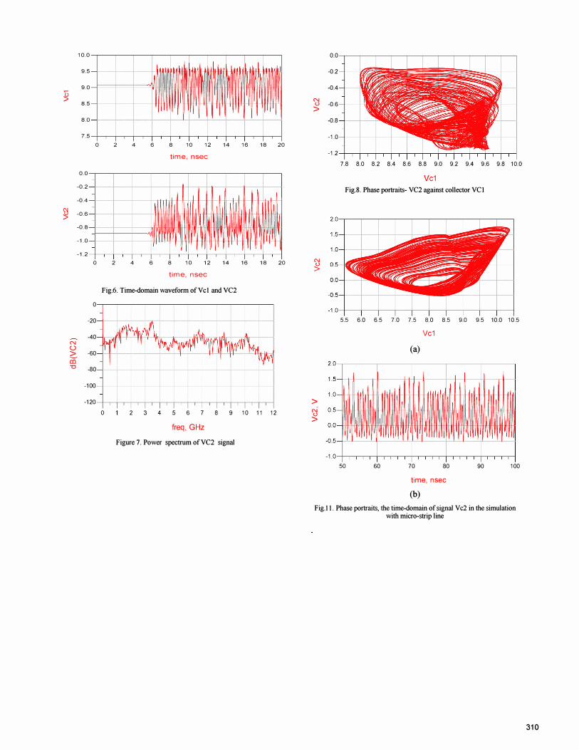
By using tuning function in ADS, following circuit parameters are chosen: Vl=V2=lOV, Cl=C2=2 pF, Re=400 Ohm, Rl=35 Ohm, R2=3.5 Ohm and the inductor L certainly equal to zero. The emitter current is Io=20mA and fundamental frequency (in regard to the parasitic components) f'I' is about 3.5 GHz. The waveforms of simulated signals VCl, VC2 are shown in Fig.6. It can be seen that the circuit goes into chaotic state in about 7 nanoseconds. The chaotic attractor VCl versus VC2 is shown in figure 7. Spectrum distribution of signal VC2 is presented in Fig.8. These three graphs demonstrate randomness of signal in time domain, phase plane and frequency domain respectively.
Comparing the attractor in Fig.7 with that of numerical analysis of original improved chaotic Colpitts circuit in Fig.2, the attractor shapes are totally different. This is due to the parasitic components of the transistor when it works at high frequency. However, it is obvious that both oscillations are chaotic.
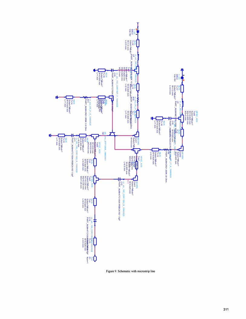
Our proposal circuit is realized in the micro-strip design. We use substrate material with thickness H=1.59mm and dielectric constant Er=2.33. All the circuit components are in SMD (Surface Mount Device) package. The schematic and layout are shown in Fig.9 and Fig.lO. The phase portrait and the signal V C2 simulated in Figure 11 show that the designed oscillator can exhibit the chaotic oscillations.
V. CONCLUSION
In this paper, we have demonstrated that the improved Colpitts oscillator with BFG425W transistor can generate wideband chaotic oscillations effectively. The numerical and simulation results show that the oscillator generates chaotic signal in designed microwave frequency band. We also design and realize the layout of this circuit in micro-strip technology. Further study will be carried out in future by experiment in real circuit and also can be extended as an oscillator for ultrawideband wireless communications.
309
10.0 0.0
9.5
t t -0.2
9.0
[ [ -0.4
� N 8.5 u -0.6 > 8.0 -0.8
7.5 -1.0 0 2 4 6 8 10 12 14 16 18 20
time, nsec -1.2
7.8 8.0 8.2 8.4 8.6 8.8 9.0 9.2 9.4 9.6 9.8 10.0 0.0
t Vc1
-0.2 Fig.8. Phase portraits-VC2 against collector VCI
-0.4
� -0.6
-0.8
-1.0
-1.2 0 2 4 6 8 10 12 14 16 18 20 N U > time, nsec
Fig.6. Time-domain waveform of Vel and VC2
0
-20 5.5 6.0 6.5 7.0 7.5 8.0 8.5 9.0 9.5 10.0 10.5
-40 Vc1 N 0 (a) G -60 co "0 -80
1 -100
-120 > 0 2 3 4 5 6 7 8 9 10 11 12 N u >
freq, GHz Figure 7. Power spectrum ofVC2 signal
-1 50 60 70 80 90 100
time, nsec (b)
Fig.11. Phase portraits, the time-domain of signal V c2 in the simulation with micro-strip line
310
� Q.
.� § e -5 '� t,)
'! "5 en
0\ � 6h �
;;;
Vc1
MC
OR
NC
orn4
W=0.8 m
mS
ubst="MS
ub1"
sl_act_MIC
1206_K_19960828
L9PA
RT
_NU
M=M
IC1206-100K
10 uH
MLIN
TL10
L=1 mm
W=0.625 m
mS
ubst="MS
ub1"
sc_atc_100_CD
R11B
G_B
_19960828C
11P
AR
T_N
UM
=AT
C100A
1R5B
CA
150 1.5pF
Port
P1
Num
=1
MLIN
TL13
L=2.5 mm
W=0.625 m
mS
ubst="MS
ub1"
MLIN
TL19
L=1 mm
W=0.625 m
mS
ubst="MS
ub1"
MLIN
TL18
L=1 mm
W=0.625 m
mS
ubst="MS
ub1"
MLIN
TL4
L=0.5 mm
W=0.625 m
mS
ubst="MS
ub1"
MLIN
TL5
L=0.325 mm
W=0.625 m
mS
ubst="MS
ub1"
MT
EE
_AD
ST
ee6
W3=3 m
mW
2=0.625 mm
W1=0.625 m
mS
ubst="MS
ub1"
MT
EE
_AD
ST
ee7
W3=3 m
mW
2=0.625 mm
W1=0.625 m
mS
ubst="MS
ub1"
MLIN
TL15
L=2 mm
W=0.625 m
mS
ubst="MS
ub1"
MLIN
TL14
L=1 mm
W=0.625 m
mS
ubst="MS
ub1"
MLIN
TL1
L=1 mm
W=0.625 m
mS
ubst="MS
ub1"
MLIN
TL3
L=6 mm
W=0.625 m
mS
ubst="MS
ub1"
sc_atc_700_CD
R11B
P_F_19960828
C19
PA
RT
_NU
M=A
TC
700A331FC
A150 330pF
MLIN
TL8
L=1 mm
W=0.625 m
mS
ubst="MS
ub1"
sc_atc_700_CD
R11B
P_F_19960828
C18
PA
RT
_NU
M=A
TC
700A331FC
A150 330pF
sl_act_MIC
1206_K_19960828
L8PA
RT
_NU
M=M
IC1206-100K
10 uH
MLIN
TL12
L=2 mm
W=0.625 m
mS
ubst="MS
ub1"
V_D
CS
RC
3V
dc=9V
MLIN
TL16
L=2.5 mm
W=1.5 m
mS
ubst="MS
ub1"
V_D
CS
RC
2V
dc=9V
MLIN
TL17
L=2.5 mm
W=1.5 m
mS
ubst="MS
ub1"
MC
OR
NC
orn1
W=0.8 m
mS
ubst="MS
ub1"
pb_sms_B
FP136W
_19960901Q
2
MC
OR
NC
orn3
W=0.625 m
mS
ubst="MS
ub1"sr_avx_C
R_21_K
_19960828R
10P
AR
T_N
UM
=CR
21-511K 510 O
hm
MT
EE
_AD
ST
ee5
W3=0.8 m
mW
2=0.8 mm
W1=0.8 m
mS
ubst="MS
ub1"M
TE
E_A
DS
Tee3
W3=1.25 m
mW
2=0.725 mm
W1=0.725 m
mS
ubst="MS
ub1"M
LINT
L9
L=0.5 mm
W=0.625 m
mS
ubst="MS
ub1"
MLIN
TL6
L=0.5 mm
W=0.625 m
mS
ubst="MS
ub1"
sc_atc_100_CD
R11B
G_B
_19960828C
10P
AR
T_N
UM
=AT
C100A
1R0B
CA
150 1pF
MC
OR
NC
orn2
W=0.625 m
mS
ubst="MS
ub1"
sr_avx_CR
_21_K_19960828
R9
PA
RT
_NU
M=C
R21-300K
30 Ohmsc_atc_100_C
DR
11BG
_B_19960828
C12
PA
RT
_NU
M=A
TC
100A1R
5BC
A150 1.5pF
MT
EE
_AD
ST
ee1
W3=0.8 m
mW
2=0.625 mm
W1=0.8 m
mS
ubst="MS
ub1"
sr_avx_CR
_21_K_19960828
R11
PA
RT
_NU
M=C
R21-3R
9K 3.9 O
hm
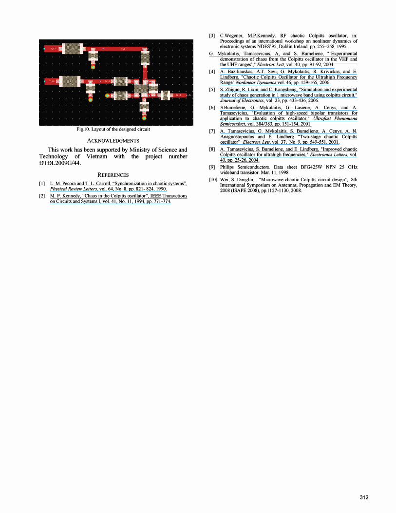
Fig.10. Layout of the designed circuit
ACKNOWLEDGMENTS
This work has been supported by Ministry of Science and Technology of Vietnam with the project number DTDL2009G/44.
REFERENCES
[I ] L. M. Pecora and I. L. Carroll, "Synchronization in chaotic systems", Physical Review Letters, vol. 64, No. 8, pp. 821- 824, 1990.
[2] M. P. Kennedy, "Chaos in the Colpitts oscillator", IEEE Transactions on Circuits and Systems I, vol. 41, No. I I , 1994, pp. 771-774.
[3] CWegener, M.P.Kennedy. RF chaotic Colpitts oscillator, in: Proceedings of an international workshop on nonlinear dynamics of electronic systems NDES'95, Dublin Ireland, pp. 255-258, 1995.
G. Mykolaitis, Tamasevicius. A, and S. Bumeliene, '''Experimental demonstration of chaos from the Colpitts oscillator in the VHF and the UHF ranges', " Electron. Lett, vol. 40, pp. 91-92, 2004.
[4] A. Baziliauskas, A.I. Sevi, G. Mykolaitis, R. Krivickas, and E. Lindberg, "Chaotic Colpitts Oscillator for the Ultrahigh Frequency Range " Nonlinear Dynamics,vol. 46, pp. 159-165, 2006.
[5] S. Zhiguo, R. Lixin, and C. Kangsheng, "Simulation and experimental study of chaos generation in I microwave band using colpitts circuit, " Journal of Electronics, vol. 23, pp. 433-436, 2006.
[6] S.Bumeliene, G. Mykolaitis, G. Lasiene, A. Cenys, and A. Tamasevicius, "Evaluation of high-speed bipolar transistors for application to chaotic colpitts oscillator, " Ultrafast Phenomena Semiconduct, vol. 384/383, pp. 151-154, 2001.
[7] A. Tamasevicius, G. Mykolaitis, S. Bumelieno, A. Cenys, A. N. Anagnostopoulos and E. Lindberg "Two-stage chaotic Colpitts oscillator" Electron. Lett, vol. 37, No. 9, pp. 549-551, 2001.
[8] A. Tamasevicius, S. Bumeliene, and E. Lindberg, "Improved chaotic Colpitts oscillator for ultrahigh frequencies, " Electronics Letters, vol. 40, pp. 25-26, 2004.
[9] Philips Semiconductors. Data sheet BFG425W NPN 25 GHz wideband transistor. Mar. 11, 1998.
[10] Wei; S. Donglin; , "Microwave chaotic Colpitts circuit design ", 8th International Symposium on Antennas, Propagation and EM Theory, 2008 (ISAPE 2008), pp.1127-1 130, 2008.
312
Copyright © 2022 FDOKUMEN