Single-chip CMOS pulse generator for UWB systems
11
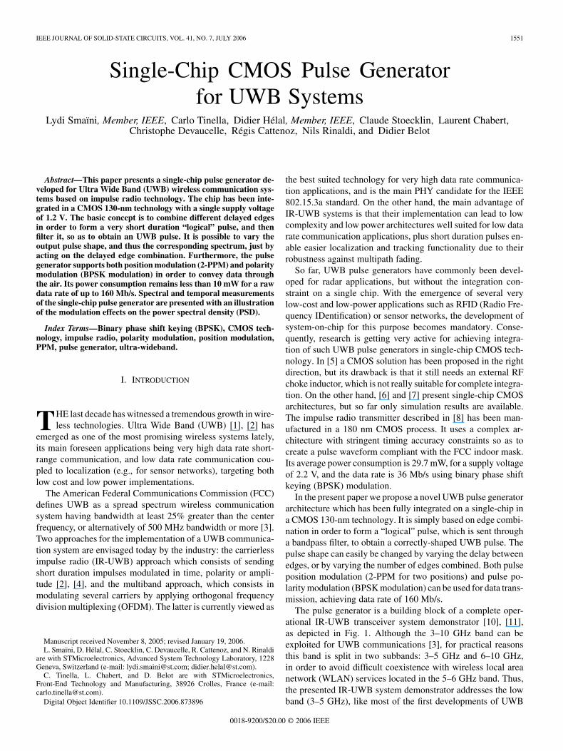
IEEE JOURNAL OF SOLID-STATE CIRCUITS, VOL. 41, NO. 7, JULY 2006 1551 Single-Chip CMOS Pulse Generator for UWB Systems Lydi Smaïni, Member, IEEE, Carlo Tinella, Didier Hélal, Member, IEEE, Claude Stoecklin, Laurent Chabert, Christophe Devaucelle, Régis Cattenoz, Nils Rinaldi, and Didier Belot Abstract—This paper presents a single-chip pulse generator de- veloped for Ultra Wide Band (UWB) wireless communication sys- tems based on impulse radio technology. The chip has been inte- grated in a CMOS 130-nm technology with a single supply voltage of 1.2 V. The basic concept is to combine different delayed edges in order to form a very short duration “logical” pulse, and then filter it, so as to obtain an UWB pulse. It is possible to vary the output pulse shape, and thus the corresponding spectrum, just by acting on the delayed edge combination. Furthermore, the pulse generator supports both position modulation (2-PPM) and polarity modulation (BPSK modulation) in order to convey data through the air. Its power consumption remains less than 10 mW for a raw data rate of up to 160 Mb/s. Spectral and temporal measurements of the single-chip pulse generator are presented with an illustration of the modulation effects on the power spectral density (PSD). Index Terms—Binary phase shift keying (BPSK), CMOS tech- nology, impulse radio, polarity modulation, position modulation, PPM, pulse generator, ultra-wideband. I. INTRODUCTION T HE last decade has witnessed a tremendous growth in wire- less technologies. Ultra Wide Band (UWB) [1], [2] has emerged as one of the most promising wireless systems lately, its main foreseen applications being very high data rate short- range communication, and low data rate communication cou- pled to localization (e.g., for sensor networks), targeting both low cost and low power implementations. The American Federal Communications Commission (FCC) defines UWB as a spread spectrum wireless communication system having bandwidth at least 25% greater than the center frequency, or alternatively of 500 MHz bandwidth or more [3]. Two approaches for the implementation of a UWB communica- tion system are envisaged today by the industry: the carrierless impulse radio (IR-UWB) approach which consists of sending short duration impulses modulated in time, polarity or ampli- tude [2], [4], and the multiband approach, which consists in modulating several carriers by applying orthogonal frequency division multiplexing (OFDM). The latter is currently viewed as Manuscript received November 8, 2005; revised January 19, 2006. L. Smaïni, D. Hélal, C. Stoecklin, C. Devaucelle, R. Cattenoz, and N. Rinaldi are with STMicroelectronics, Advanced System Technology Laboratory, 1228 Geneva, Switzerland (e-mail: [email protected]; [email protected]). C. Tinella, L. Chabert, and D. Belot are with STMicroelectronics, Front-End Technology and Manufacturing, 38926 Crolles, France (e-mail: [email protected]). Digital Object Identifier 10.1109/JSSC.2006.873896 the best suited technology for very high data rate communica- tion applications, and is the main PHY candidate for the IEEE 802.15.3a standard. On the other hand, the main advantage of IR-UWB systems is that their implementation can lead to low complexity and low power architectures well suited for low data rate communication applications, plus short duration pulses en- able easier localization and tracking functionality due to their robustness against multipath fading. So far, UWB pulse generators have commonly been devel- oped for radar applications, but without the integration con- straint on a single chip. With the emergence of several very low-cost and low-power applications such as RFID (Radio Fre- quency IDentification) or sensor networks, the development of system-on-chip for this purpose becomes mandatory. Conse- quently, research is getting very active for achieving integra- tion of such UWB pulse generators in single-chip CMOS tech- nology. In [5] a CMOS solution has been proposed in the right direction, but its drawback is that it still needs an external RF choke inductor, which is not really suitable for complete integra- tion. On the other hand, [6] and [7] present single-chip CMOS architectures, but so far only simulation results are available. The impulse radio transmitter described in [8] has been man- ufactured in a 180 nm CMOS process. It uses a complex ar- chitecture with stringent timing accuracy constraints so as to create a pulse waveform compliant with the FCC indoor mask. Its average power consumption is 29.7 mW, for a supply voltage of 2.2 V, and the data rate is 36 Mb/s using binary phase shift keying (BPSK) modulation. In the present paper we propose a novel UWB pulse generator architecture which has been fully integrated on a single-chip in a CMOS 130-nm technology. It is simply based on edge combi- nation in order to form a “logical” pulse, which is sent through a bandpass filter, to obtain a correctly-shaped UWB pulse. The pulse shape can easily be changed by varying the delay between edges, or by varying the number of edges combined. Both pulse position modulation (2-PPM for two positions) and pulse po- larity modulation (BPSK modulation) can be used for data trans- mission, achieving data rate of 160 Mb/s. The pulse generator is a building block of a complete oper- ational IR-UWB transceiver system demonstrator [10], [11], as depicted in Fig. 1. Although the 3–10 GHz band can be exploited for UWB communications [3], for practical reasons this band is split in two subbands: 3–5 GHz and 6–10 GHz, in order to avoid difficult coexistence with wireless local area network (WLAN) services located in the 5–6 GHz band. Thus, the presented IR-UWB system demonstrator addresses the low band (3–5 GHz), like most of the first developments of UWB 0018-9200/$20.00 © 2006 IEEE
-
Upload
independent -
Category
Documents
-
view
4 -
download
0
Transcript of Single-chip CMOS pulse generator for UWB systems
IEEE JOURNAL OF SOLID-STATE CIRCUITS, VOL. 41, NO. 7, JULY 2006 1551
Single-Chip CMOS Pulse Generatorfor UWB Systems
Lydi Smaïni, Member, IEEE, Carlo Tinella, Didier Hélal, Member, IEEE, Claude Stoecklin, Laurent Chabert,Christophe Devaucelle, Régis Cattenoz, Nils Rinaldi, and Didier Belot
Abstract—This paper presents a single-chip pulse generator de-veloped for Ultra Wide Band (UWB) wireless communication sys-tems based on impulse radio technology. The chip has been inte-grated in a CMOS 130-nm technology with a single supply voltageof 1.2 V. The basic concept is to combine different delayed edgesin order to form a very short duration “logical” pulse, and thenfilter it, so as to obtain an UWB pulse. It is possible to vary theoutput pulse shape, and thus the corresponding spectrum, just byacting on the delayed edge combination. Furthermore, the pulsegenerator supports both position modulation (2-PPM) and polaritymodulation (BPSK modulation) in order to convey data throughthe air. Its power consumption remains less than 10 mW for a rawdata rate of up to 160 Mb/s. Spectral and temporal measurementsof the single-chip pulse generator are presented with an illustrationof the modulation effects on the power spectral density (PSD).
Index Terms—Binary phase shift keying (BPSK), CMOS tech-nology, impulse radio, polarity modulation, position modulation,PPM, pulse generator, ultra-wideband.
I. INTRODUCTION
THE last decade has witnessed a tremendous growth in wire-less technologies. Ultra Wide Band (UWB) [1], [2] has
emerged as one of the most promising wireless systems lately,its main foreseen applications being very high data rate short-range communication, and low data rate communication cou-pled to localization (e.g., for sensor networks), targeting bothlow cost and low power implementations.
The American Federal Communications Commission (FCC)defines UWB as a spread spectrum wireless communicationsystem having bandwidth at least 25% greater than the centerfrequency, or alternatively of 500 MHz bandwidth or more [3].Two approaches for the implementation of a UWB communica-tion system are envisaged today by the industry: the carrierlessimpulse radio (IR-UWB) approach which consists of sendingshort duration impulses modulated in time, polarity or ampli-tude [2], [4], and the multiband approach, which consists inmodulating several carriers by applying orthogonal frequencydivision multiplexing (OFDM). The latter is currently viewed as
Manuscript received November 8, 2005; revised January 19, 2006.L. Smaïni, D. Hélal, C. Stoecklin, C. Devaucelle, R. Cattenoz, and N. Rinaldi
are with STMicroelectronics, Advanced System Technology Laboratory, 1228Geneva, Switzerland (e-mail: [email protected]; [email protected]).
C. Tinella, L. Chabert, and D. Belot are with STMicroelectronics,Front-End Technology and Manufacturing, 38926 Crolles, France (e-mail:[email protected]).
Digital Object Identifier 10.1109/JSSC.2006.873896
the best suited technology for very high data rate communica-tion applications, and is the main PHY candidate for the IEEE802.15.3a standard. On the other hand, the main advantage ofIR-UWB systems is that their implementation can lead to lowcomplexity and low power architectures well suited for low datarate communication applications, plus short duration pulses en-able easier localization and tracking functionality due to theirrobustness against multipath fading.
So far, UWB pulse generators have commonly been devel-oped for radar applications, but without the integration con-straint on a single chip. With the emergence of several verylow-cost and low-power applications such as RFID (Radio Fre-quency IDentification) or sensor networks, the development ofsystem-on-chip for this purpose becomes mandatory. Conse-quently, research is getting very active for achieving integra-tion of such UWB pulse generators in single-chip CMOS tech-nology. In [5] a CMOS solution has been proposed in the rightdirection, but its drawback is that it still needs an external RFchoke inductor, which is not really suitable for complete integra-tion. On the other hand, [6] and [7] present single-chip CMOSarchitectures, but so far only simulation results are available.The impulse radio transmitter described in [8] has been man-ufactured in a 180 nm CMOS process. It uses a complex ar-chitecture with stringent timing accuracy constraints so as tocreate a pulse waveform compliant with the FCC indoor mask.Its average power consumption is 29.7 mW, for a supply voltageof 2.2 V, and the data rate is 36 Mb/s using binary phase shiftkeying (BPSK) modulation.
In the present paper we propose a novel UWB pulse generatorarchitecture which has been fully integrated on a single-chip ina CMOS 130-nm technology. It is simply based on edge combi-nation in order to form a “logical” pulse, which is sent througha bandpass filter, to obtain a correctly-shaped UWB pulse. Thepulse shape can easily be changed by varying the delay betweenedges, or by varying the number of edges combined. Both pulseposition modulation (2-PPM for two positions) and pulse po-larity modulation (BPSK modulation) can be used for data trans-mission, achieving data rate of 160 Mb/s.
The pulse generator is a building block of a complete oper-ational IR-UWB transceiver system demonstrator [10], [11],as depicted in Fig. 1. Although the 3–10 GHz band can beexploited for UWB communications [3], for practical reasonsthis band is split in two subbands: 3–5 GHz and 6–10 GHz,in order to avoid difficult coexistence with wireless local areanetwork (WLAN) services located in the 5–6 GHz band. Thus,the presented IR-UWB system demonstrator addresses the lowband (3–5 GHz), like most of the first developments of UWB
0018-9200/$20.00 © 2006 IEEE
1552 IEEE JOURNAL OF SOLID-STATE CIRCUITS, VOL. 41, NO. 7, JULY 2006
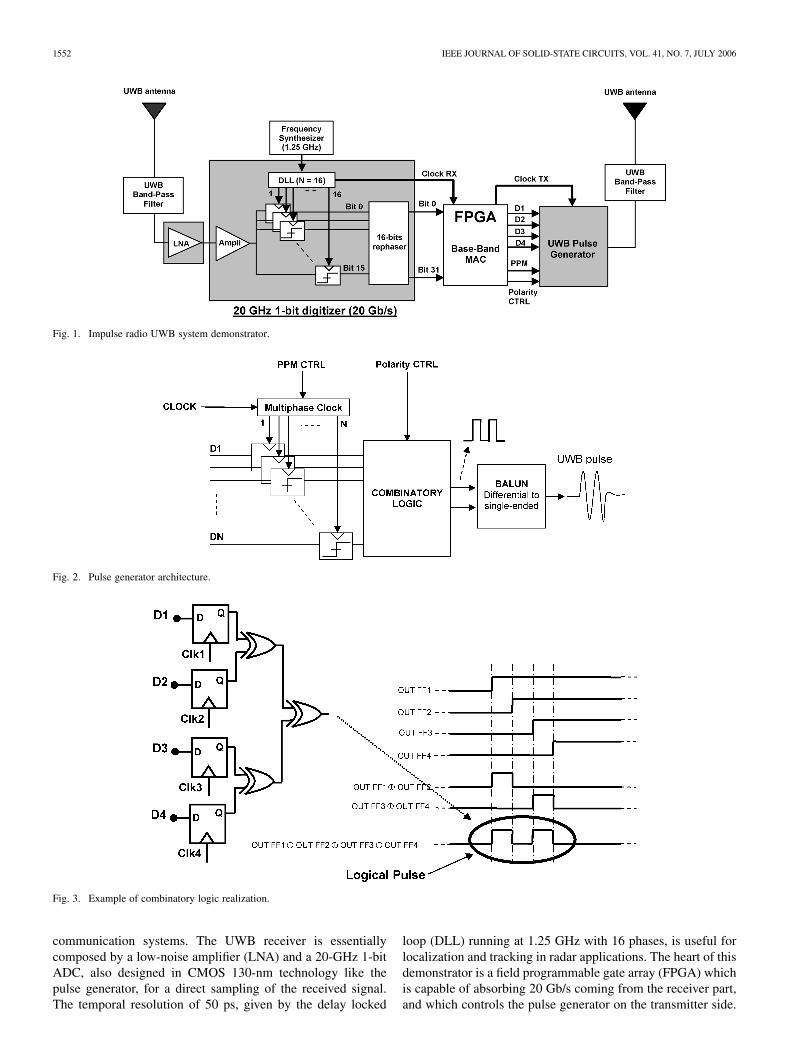
Fig. 1. Impulse radio UWB system demonstrator.
Fig. 2. Pulse generator architecture.
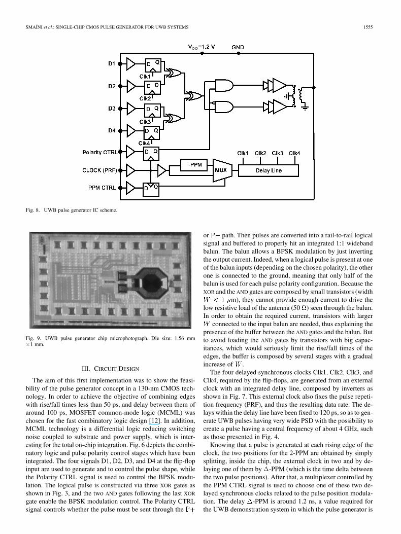
Fig. 3. Example of combinatory logic realization.
communication systems. The UWB receiver is essentiallycomposed by a low-noise amplifier (LNA) and a 20-GHz 1-bitADC, also designed in CMOS 130-nm technology like thepulse generator, for a direct sampling of the received signal.The temporal resolution of 50 ps, given by the delay locked
loop (DLL) running at 1.25 GHz with 16 phases, is useful forlocalization and tracking in radar applications. The heart of thisdemonstrator is a field programmable gate array (FPGA) whichis capable of absorbing 20 Gb/s coming from the receiver part,and which controls the pulse generator on the transmitter side.

SMAÏNI et al.: SINGLE-CHIP CMOS PULSE GENERATOR FOR UWB SYSTEMS 1553
Fig. 4. UWB pulses simulated for two combinations of edges (left graphs: 2 edges, right graphs: 4 edges).
It embeds digital baseband processing (modulation/demodula-tion, channel estimation, synchronization, channel coding), anda simplified medium access control (MAC) module.
This paper is organized as follows. Section II describes theUWB pulse generator architecture. The circuit design is dealtwith in Section III. Section IV presents experimental results inthe temporal and spectral domains. Finally, Section V summa-rizes the paper.
II. PULSE GENERATOR ARCHITECTURE
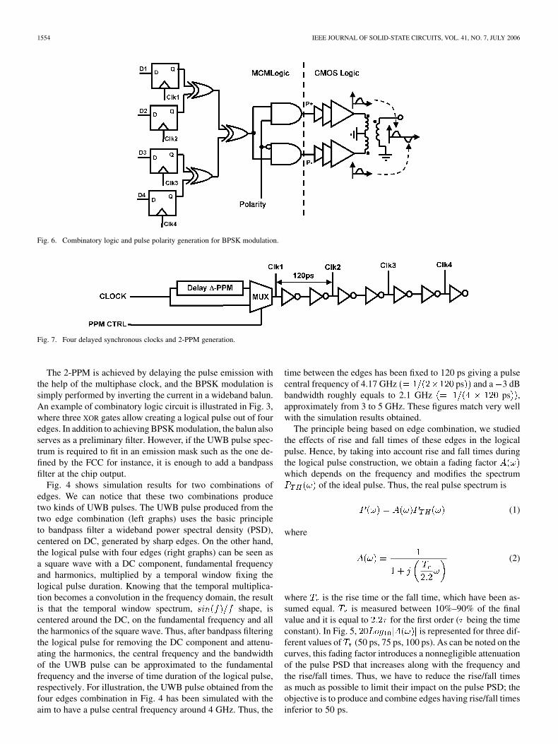
The complete pulse generator architecture comprisesflip-flops, a multiphase clock, combinatory logic and a balun,as depicted in Fig. 2. The basic concept is to combine differentdelayed edges by latching the flip-flops with delayed syn-chronous clocks so as to form a very short duration “logical”pulse, and then to filter it, in order to generate an UWB pulse.This short-duration pulse corresponds to a wide spectrum inthe frequency domain since the pulse bandwidth is inverselyproportional to its duration in time. Although not dedicated toUWB, delayed synchronous clocks and combination of edgeshave been already used to synthesize a signal like in [9], where
Fig. 5. Representation of 20Log jA(!)j for three values of rise/fall time T .
a circuit converts a square wave signal in both in-phase andquadrature-phase sinusoidal differential outputs.
1554 IEEE JOURNAL OF SOLID-STATE CIRCUITS, VOL. 41, NO. 7, JULY 2006
Fig. 6. Combinatory logic and pulse polarity generation for BPSK modulation.
Fig. 7. Four delayed synchronous clocks and 2-PPM generation.
The 2-PPM is achieved by delaying the pulse emission withthe help of the multiphase clock, and the BPSK modulation issimply performed by inverting the current in a wideband balun.An example of combinatory logic circuit is illustrated in Fig. 3,where three XOR gates allow creating a logical pulse out of fouredges. In addition to achieving BPSK modulation, the balun alsoserves as a preliminary filter. However, if the UWB pulse spec-trum is required to fit in an emission mask such as the one de-fined by the FCC for instance, it is enough to add a bandpassfilter at the chip output.
Fig. 4 shows simulation results for two combinations ofedges. We can notice that these two combinations producetwo kinds of UWB pulses. The UWB pulse produced from thetwo edge combination (left graphs) uses the basic principleto bandpass filter a wideband power spectral density (PSD),centered on DC, generated by sharp edges. On the other hand,the logical pulse with four edges (right graphs) can be seen asa square wave with a DC component, fundamental frequencyand harmonics, multiplied by a temporal window fixing thelogical pulse duration. Knowing that the temporal multiplica-tion becomes a convolution in the frequency domain, the resultis that the temporal window spectrum, shape, iscentered around the DC, on the fundamental frequency and allthe harmonics of the square wave. Thus, after bandpass filteringthe logical pulse for removing the DC component and attenu-ating the harmonics, the central frequency and the bandwidthof the UWB pulse can be approximated to the fundamentalfrequency and the inverse of time duration of the logical pulse,respectively. For illustration, the UWB pulse obtained from thefour edges combination in Fig. 4 has been simulated with theaim to have a pulse central frequency around 4 GHz. Thus, the
time between the edges has been fixed to 120 ps giving a pulsecentral frequency of 4.17 GHz ps and a 3 dBbandwidth roughly equals to 2.1 GHz ps ,approximately from 3 to 5 GHz. These figures match very wellwith the simulation results obtained.
The principle being based on edge combination, we studiedthe effects of rise and fall times of these edges in the logicalpulse. Hence, by taking into account rise and fall times duringthe logical pulse construction, we obtain a fading factorwhich depends on the frequency and modifies the spectrum
of the ideal pulse. Thus, the real pulse spectrum is
(1)
where
(2)
where is the rise time or the fall time, which have been as-sumed equal. is measured between 10%–90% of the finalvalue and it is equal to for the first order ( being the timeconstant). In Fig. 5, is represented for three dif-ferent values of (50 ps, 75 ps, 100 ps). As can be noted on thecurves, this fading factor introduces a nonnegligible attenuationof the pulse PSD that increases along with the frequency andthe rise/fall times. Thus, we have to reduce the rise/fall timesas much as possible to limit their impact on the pulse PSD; theobjective is to produce and combine edges having rise/fall timesinferior to 50 ps.
SMAÏNI et al.: SINGLE-CHIP CMOS PULSE GENERATOR FOR UWB SYSTEMS 1555
Fig. 8. UWB pulse generator IC scheme.
Fig. 9. UWB pulse generator chip microphotograph. Die size: 1.56 mm�1 mm.
III. CIRCUIT DESIGN
The aim of this first implementation was to show the feasi-bility of the pulse generator concept in a 130-nm CMOS tech-nology. In order to achieve the objective of combining edgeswith rise/fall times less than 50 ps, and delay between them ofaround 100 ps, MOSFET common-mode logic (MCML) waschosen for the fast combinatory logic design [12]. In addition,MCML technology is a differential logic reducing switchingnoise coupled to substrate and power supply, which is inter-esting for the total on-chip integration. Fig. 6 depicts the combi-natory logic and pulse polarity control stages which have beenintegrated. The four signals D1, D2, D3, and D4 at the flip-flopinput are used to generate and to control the pulse shape, whilethe Polarity CTRL signal is used to control the BPSK modu-lation. The logical pulse is constructed via three XOR gates asshown in Fig. 3, and the two AND gates following the last XOR
gate enable the BPSK modulation control. The Polarity CTRLsignal controls whether the pulse must be sent through the
or path. Then pulses are converted into a rail-to-rail logicalsignal and buffered to properly hit an integrated 1:1 widebandbalun. The balun allows a BPSK modulation by just invertingthe output current. Indeed, when a logical pulse is present at oneof the balun inputs (depending on the chosen polarity), the otherone is connected to the ground, meaning that only half of thebalun is used for each pulse polarity configuration. Because theXOR and the AND gates are composed by small transistors (width
m), they cannot provide enough current to drive thelow resistive load of the antenna (50 ) seen through the balun.In order to obtain the required current, transistors with larger
connected to the input balun are needed, thus explaining thepresence of the buffer between the AND gates and the balun. Butto avoid loading the AND gates by transistors with big capac-itances, which would seriously limit the rise/fall times of theedges, the buffer is composed by several stages with a gradualincrease of .
The four delayed synchronous clocks Clk1, Clk2, Clk3, andClk4, required by the flip-flops, are generated from an externalclock with an integrated delay line, composed by inverters asshown in Fig. 7. This external clock also fixes the pulse repeti-tion frequency (PRF), and thus the resulting data rate. The de-lays within the delay line have been fixed to 120 ps, so as to gen-erate UWB pulses having very wide PSD with the possibility tocreate a pulse having a central frequency of about 4 GHz, suchas those presented in Fig. 4.
Knowing that a pulse is generated at each rising edge of theclock, the two positions for the 2-PPM are obtained by simplysplitting, inside the chip, the external clock in two and by de-laying one of them by -PPM (which is the time delta betweenthe two pulse positions). After that, a multiplexer controlled bythe PPM CTRL signal is used to choose one of these two de-layed synchronous clocks related to the pulse position modula-tion. The delay -PPM is around 1.2 ns, a value required forthe UWB demonstration system in which the pulse generator is
1556 IEEE JOURNAL OF SOLID-STATE CIRCUITS, VOL. 41, NO. 7, JULY 2006
Fig. 10. Evaluation board picture.
utilized. The circuit designed for the 2-PPM generation is alsodepicted in Fig. 7.
The generation of the four synchronous clocks, relying onopen-loop inverter propagation delays, does introduce processand temperature dependencies and therefore would not be viablefor the final implementation of the complete transceiver. How-ever, this first implementation for the IR-UWB demonstratoraims to show the feasibility of the pulse generator concept, thusan oversimplified timing solution has been preferred to more re-liable ones. Consequently, in our future developments in whichthe pulse generator and the receiver will be integrated on thesame transceiver chip, all the delays and the pulse position mod-ulation will be managed by the DLL already operational in thereceiver chip, in order to overcome these process and tempera-ture variations.
Fig. 8 shows a schematic of the UWB pulse generator IC, andFig. 9 depicts a microphotograph of the die, in which the inte-grated balun used for BPSK modulation can clearly be seen onthe right side. The chip was processed in an STMicroelectronicsCMOS 130-nm technology using only basic gate oxide transis-tors (20 ), six metal layers, and metal–insulator–metal (MIM)capacitors. The resulting die area is 1.56 mm .
IV. MEASUREMENT RESULTS
The pulse generator evaluation board (Fig. 10) is composed ofa mother board with various I/Os, and a daughter board in whichthe TX chip is directly bonded. The mother board includes threeSMA inputs used to control the pulse generator:
— Clock In: External clock fixing the PRF;— PPM Ctrl: 2-PPM control;— Polarity Ctrl: BPSK modulation control.
There is also a SCSI (Small Computer System Interface) con-nector which is used to control the pulse shape (and which canalso be used to generate the modulations if desired) from theFPGA of the IR-UWB system demonstrator.
The pulse generator consumes less than 10 mW for a PRFof 80 MHz, corresponding to a data rate of 160 Mb/s (2 bitsare sent per symbol, assuming a combined 2-PPM and BPSKmodulation).
A. Chip Output Pulses
The following measurements have been performed witha 20 GHz direct sampling oscilloscope (200 GHz in rep-etition) for the temporal pulse shape measurements, and aspectrum analyzer (dBm/MHz from 500 MHz to 5.5 GHz)for pulse PSD measurements. The PSD’s have been measuredby enabling both 2-PPM and BPSK modulation, generated bypseudo-random sequence generators, with a PRF of 80 MHzemulating a data rate of 160 Mb/s.
Fig. 11 and Fig. 12 show two different pulse shapes generatedfor the two edge combinations corresponding to the simulationspresented in Fig. 4. On each of the PSD diagrams, the indoorFCC mask has been represented.
The pulse shape 1 (Fig. 11) is generated by combining twoedges separated by the minimum delay, i.e., 120 ps, in order togenerate a very wide spectrum. We obtain at the chip output,after the balun filtering, an UWB pulse with peak-to-peak am-plitude of 450 mV and a duration around 600 ps. The resultingtemporal shape resembles very closely the simulated one (pre-sented in Fig. 4, left-hand side). As expected, its PSD spans overa large bandwidth with a 10 dB bandwidth of 4 GHz (from1 GHz to 5 GHz) and a maximum value of 50 dBm/MHz.

SMAÏNI et al.: SINGLE-CHIP CMOS PULSE GENERATOR FOR UWB SYSTEMS 1557
Fig. 11. Chip output pulse 1—temporal shape (x: 200 ps/div, y: 100 mV/div) and PSD (Start: 500 MHz, Span: 5 GHz, RBW: 1 MHz, Ref Lvl: �30 dBm,10 dB/div).
Fig. 12. Chip output pulse 2—temporal shape (x: 200 ps/div, y: 100 mV/div) and PSD (Start: 500 MHz, Span: 5 GHz, RBW: 1 MHz, Ref Lvl: �30 dBm,10 dB/div).
The pulse shape 2 is obtained by combining four edges to gen-erate an UWB pulse having a central frequency around 4 GHz(Fig. 12). The duration is about 800 ps and its peak-to-peakamplitude is around 350 mV. Its temporal shape and its PSDare very similar to the ones simulated in the previous section(Fig. 4, right-hand side). As expected, its PSD presents a max-imum around 4 GHz and a hole just above 2 GHz.
We can see that the two pulses presented above are not FCCcompliant and thus a bandpass filter is necessary at the chipoutput. Fig. 13 represents the chip output pulse 2 bandpass fil-tered between 3.1 and 5 GHz. The result in the temporal do-main is an increase of the pulse duration due to the fact that wehave reduced the PSD bandwidth to be FCC compliant above3.1 GHz.
Measurements depicted in Fig. 14 show the correct operationof the two modulations supported by the pulse generator: theBPSK modulation and the two positions of the 2-PPM can beobserved. A slight mismatch in amplitude on the BPSK modu-lation can be noticed, certainly due to a non perfect symmetryin the balun. On the other hand, the time difference between thetwo positions of the 2-PPM is 1.2 ns as expected.
B. Pulse Modulation Effects on the Power Spectral Density
This characterization consists in showing the effects of BPSKmodulation and 2-PPM on the spectrum, by measuring the UWBpulse PSD in dBm/MHz, from 500 MHz to 5.5 GHz. The pulsedepicted in Fig. 11 (pulse shape 1) has been used for these

1558 IEEE JOURNAL OF SOLID-STATE CIRCUITS, VOL. 41, NO. 7, JULY 2006
Fig. 13. Chip Output Pulse 2 bandpass filtered in order to be compliant with FCC indoor emission mask—temporal shape (x: 500 ps/div, y: 50 mV/div) and PSD(Start: 500 MHz, Span: 5 GHz, RBW: 1 MHz, Ref Lvl: �30 dBm, 10 dB/div).
Fig. 14. Pulse modulations: BPSK (left) and 2-PPM (right)—(x: 200 ps/div, y: 100 mV/div).
measurements and pseudo-random sequence generators emu-late data modulation at 160 Mb/s. Fig. 15 shows the four cases:no modulation, 2-PPM on, BPSK on, both BPSK and 2-PPMon.
If the pulse train is not modulated, a discrete spectrum results,and the PSD is composed by rays as predicted by the theory.The distance between rays corresponds to the chosen PRF (inthis case 80 MHz). On the other hand, the rays are reduced (oreven disappear altogether) on the PSD just by enabling pulsemodulation (2-PPM and/or BPSK) because the pulse periodicityis broken. Indeed, the modulation whitens the PSD by spreadingthe rays’ energy across the spectrum, which is very important inorder to efficiently fit the regulatory emission mask that limitsthe maximum PSD. BPSK modulation is clearly more efficientfor the PSD whitening than 2-PPM. Thus, in a narrow band,the UWB modulated pulse transmission can be assimilated to awhite noise.
V. SUMMARY
This paper has presented the architecture, design, and in-tegration of a single chip UWB pulse generator in 130-nmCMOS technology. The implemented chip offers the possi-bility to change the output pulse shape by using different edgecombinations. Pulses can be modulated in position (2-PPM)and polarity (BPSK) so as to convey information for wirelesscommunication applications. The resulting RF core of the pulsegenerator consumes less than 10 mW from a voltage supply of1.2 V and a constant data rate of 160 Mb/s. Laboratory mea-surements have confirmed the pre-design simulation previsionsregarding pulse shape, central frequency and bandwidth of aselected set of pulse shapes. They also showed that spectralrays are efficiently reduced by using both polarity and positionmodulations to the pulse train. This is important in order tofit more accurately the regulator’s spectral mask, and thus formaking better use of the available spectrum.

SMAÏNI et al.: SINGLE-CHIP CMOS PULSE GENERATOR FOR UWB SYSTEMS 1559
Fig. 15. Pulse modulation effects on the PSD—(Start: 500 MHz, Span: 5 GHz, RBW: 1 MHz, Ref Lvl: �30 dBm, 10 dB/div).
ACKNOWLEDGMENT
The authors would like to thank CEA-LETI (Grenoble,France), in particular D. Morche and P. Vincent, for the suc-cessful collaboration regarding the RF receiver development ofthe IR-UWB system demonstrator.
REFERENCES
[1] M. Pezzin, J. Keignart, N. Daniele, S. de Rivaz, B. Denis, D. Morche, P.Rouzet, R. Cattenoz, and N. Rinaldi, “Ultra wideband: the radio link ofthe future?,” Annales des Télécommunications, vol. 58, no. 3–4, Mar.–Apr. 2003.
[2] M. Z. Win and R. A. Scholtz, “Impulse radio: how it works,” IEEECommun. Lett., vol. 2, no. 2, pp. 36–38, Feb. 1998.
[3] First Report and Order: Revision of Part 15 of the Commission’s RulesRegarding Ultra-Wideband Transmission Systems Federal Communi-cations Commission (FCC), ET Docket 98-153, Adopted February 14,2002, Released Apr. 22, 2002.
[4] M. Z. Win and R. A. Scholtz, “Ultra-wide bandwidth time-hoppingspread-spectrum impulse radio for wireless multiple-access communi-cations,” IEEE Trans. Commun., vol. 17, no. 5, pp. 824–836, Apr. 2000.
[5] K. Marsden, H. J. Lee, D. Ha, and H. S. Lee, “Low power CMOSre-programmable pulse generator for UWB systems,” in IEEE Conf.UWB Systems and Technologies, Nov. 2003, pp. 443–447.
[6] S. Bagga, W. A. Serdijn, and J. R. Long, “A PPM Gaussian monocycletransmitter for ultra-wideband communications,” in Proc. IEEE JointInt. Workshop of UWBST and IWUWBS, May 2004, pp. 130–134.
[7] Y. Jeong, S. Jung, and J. Liu, “A CMOS impulse generator for UWBwireless communication systems,” in IEEE Int. Symp. Circuits and Sys-tems, May 2004, pp. 129–132.
[8] T. Norimatsu, R. Fujiwara, M. Kokubo, M. Miyazaki, Y. Ookuma, M.Hayakawa, S. Kobayashi, N. Koshizuka, and K. Sakamura, “A novelUWB impulse-radio transmitter with all-digitally-controlled pulse gen-erator,” in Proc. Eur. Solid-State Circuits Conf. (ESSCIRC), Sep. 2005,pp. 267–270.
[9] A. Spataro, Y. Deval, J.-B. Bégueret, P. Fouillat, and D. Belot, “AVLSI CMOS delay oriented waveform converter for polyphase fre-quency synthesizer,” IEEE J. Solid-State Circuits, vol. 37, no. 3, pp.336–341, Mar. 2002.
[10] D. Hélal, L. Smaïni, and C. Tinella, “Pulse-based architecture for UWBcommunication systems,” presented at the Mediterranean MicrowaveSymp., Marseille, France, Jun. 2004.
[11] D. Hélal, H. Kaaja, and L. Blazevic, “ UWB file transfer between mo-bile terminals using multi-media card standard interface and Bluetoothas a control radio,” in IEEE Int. Conf. Ultra-Wideband, Zurich, Switzer-land, Sep. 2005, pp. 609–614.
[12] M. Green and U. Singh, “Design of CMOS CML circuits for high speedbroadband communications,” in IEEE Int. Symp. Circuits and Systems,May 2003, vol. 2, pp. 204–207.
1560 IEEE JOURNAL OF SOLID-STATE CIRCUITS, VOL. 41, NO. 7, JULY 2006
Lydi Smaïni (M’06) was born in Tizi-Ouzou,Algeria, on July 27, 1974. He received the M.S. andPh.D. degrees in electronics from the Universityof South Toulon-Var, France, in 1998 and 2001,respectively, specializing in radio propagation,telecommunications and remote sensing. His thesiswork focused on pulse compression techniques andsignal processing for atmospheric radars.
After graduation, he worked as an R&D Con-sulting Engineer for ALTEN, Marseille, France,for one year. During this period, he was involved,
along with the company SERPE-IESM, Lorient, France, in the developmentof a frequency agile radar beacon for navigation aid, which is now in serviceon the French littoral. He joined STMicroelectronics in October 2002, inthe RF System and Architecture Group for wireless communications, withinthe Advanced System Technology Laboratory in Geneva, Switzerland. Hehas contributed to ST’s IEEE 802.15.3a standard proposal and the UltraWideBand Impulse Radio demonstrator. Presently, he works on advanced radioarchitectures, especially for OFDMA technology, in the product group Home,Personal, Communication.
Carlo Tinella was born in Fasano, Italy, on March31, 1973. He received the M.Sc. degree in microelec-tronics from the University de Montpellier II, France,and the Ph.D. degree in electronics engineering fromthe Institut National Polytechnique de Grenoble,France, in 1999 and 2003, respectively.
In 2003, he joined STMicroelectronics within theCentral CAD and Advanced Design Solutions De-partment, where he is working on radio-frequency in-tegration in CMOS bulk and SOI technologies forcellular phone and pulsed UWB systems. His main
research interests include SOI technology, RF CMOS modeling, CMOS analogand RF circuit design for wireless systems.
Didier Hélal (M’01) was born in Draveil, France,on July 24, 1970. He received the M.Sc. degree inelectrical engineering and the Ph.D. degree in elec-trical engineering focused on high spatial resolutionremote sensing, from the University of South Toulon-Var, France, in 1995 and 2000, respectively.
In 2000, he joined the Advanced System Tech-nology division of STMicroelectronics, working inRF system design for high data rate wireless com-munications at the Geneva Laboratory, Switzerland.He is co-inventor of four patents in the field of UWB
communication systems that engendered ST’s proposal to IEEE 802.15.3a in2003. Then, he was project leader of ST’s UWB impulse radio demonstrator in0.13 �m CMOS for large file transfer between mobile terminals. His researchinterests include ultra-wideband systems, innovative SoC radio architecturesand low-power CMOS circuits. He is currently a Senior Wireless SystemResearcher working on ultra-low-power wireless sensors networks.
Claude Stoecklin was born on December 3, 1958, inGeneva, Switzerland. After an electrical-mechanicaltraining at Sodeco Saia (1974–1978), he received theCFC grade, a Federal degree of mechanic-electrician.In 1982, he received the Master in Electrical Engi-neering degree from the Geneva Engineering School,with honors.
Between 1984 and 1987, he worked at CERN (Eu-ropean Nuclear Research Center) as an Electrical En-gineer in the Power Converter Division (LEP). Hedeveloped a DC-DC management of a power supply
(250 V/75A) for the LEP accelerator ring and supervised its manufacturing. Healso took part of the design, manufacturing, and testing of four parallel powersupplies and a 37.5 kW-resonant converter electrical management (GTO). From1989 to 1992, he worked as an Engineer for Sarcem Automation where he par-ticipated in the design of automatic wiring machines, analog and digital controlcircuitry as well as I/O cards to interface the wiring machines to their digital
control panel. From 1993 to 2000, he worked for the International Red- CrossMuseum, where he was in charge of the electrical automation of the exhibitions.Simultaneously, he worked on a freelance basis, designing electronic boards em-bedding the Intel MCS51 microcontroller, for several private customers. Since2000, he has been working for STMicroelectronics as an Application Engineer,being head of the Application Laboratory. He is responsible of the testing equip-ment and component purchasing. He is in charge of designing demonstrators forconcepts validation of the RF system teams’ IPs.
Laurent Chabert began his career in January1990 by designing electronic circuits for the instru-mentation of high magnetic fields experiments atCNRS (LCMI, Grenoble, France). In 1992, he wastransferred to the European Radiation Synchrotronfacility (ESRF, Grenoble) to work on magneticscattering beamline electronics. After acquiring anengineering degree from the Conservatoire Nationaldes Arts et Metiers (CNAM, Grenoble), and a DEAin Microelectronics from the Université JosephFourier (UJF, Grenoble), he joined STMicroelec-
tronics (Crolles, France) as an RF Design Engineer in November 2000. Hismain fields of interest are integrated RF architectures, miniaturized antennasand RF systems testability.
Christophe Devaucelle was born in Paris, France,on August 6, 1978. He received the M.Sc. degreein electrical engineering from the Ecole NormaleSupérieure de Télécommunication (ENST), Paris,France, in 2002.
He joined STMicroelectronics in September2002, in the Broadband Wireless LAN group, withinthe Advanced System Technology Department,Geneva, Switzerland. His current R&D activitiesfocus on the hardware implementation on FPGA ofultra-wideband communication systems.
Régis Cattenoz was born in Charleville-Mézières,France, on 31st October 1966. He received the M.Sc.degree in electrical engineering from Supélec (ESE,Paris, France), in 1989.
After graduation, he worked as a Network Engi-neer for 10 years for Thales (formerly Thomson-CSFDetexis, formerly Dassault Electronique). He wasinvolved in the design on military electronics net-work projects and nonmilitary Hiperlan 1 wirelessdevelopment. He joined STMicroelectronics in 2001,and was involved in UWB on R&D, standardization
(IEEE 802.15.3a, WiMedia) and product design, as a Technical Leader forthe UWB team. His expertise area covers several domains, including systemanalysis (hardware/software product architecture), IC/FPGA design, RTOSembedded design, network protocols, signal processing, modeling, test andsimulation tools.
Nils Rinaldi was born in Lausanne, Switzerland,on March 2, 1976. He received the M.Sc. degree inmobile communications from the Swiss Institute ofTechnology, Lausanne (EPFL), in 2000, and fromthe Eurécom Institute, Sophia Antipolis, France.
After graduation, he worked as a Radio NetworkEngineer for L.M. Ericsson in Denmark for twoyears. During this period, he was involved in projectsrelated to GSM adaptive antenna systems, andGPRS/EDGE systems, where he dealt with fre-quency and capacity optimization issues. He joined
STMicroelectronics in April 2002, in the Broadband Wireless LAN group,within the Advanced System Technology Department, Geneva, Switzerland.His current R&D activities focus on baseband aspects of ultra-wideband

SMAÏNI et al.: SINGLE-CHIP CMOS PULSE GENERATOR FOR UWB SYSTEMS 1561
communication systems. Lately, he has been actively participating in basebandactivities (demodulation and synchronization) within the European projectsUCAN and PULSERS. He has contributed to ST’s IEEE 802.15.3a standardproposal.
Didier Belot received the D.U.T Electronique de-gree from the Institut Universitaire de Technologie,Grenoble, France, in 1982, and the M.S degree fromthe Ecole Nationale Supérieure d’Electronique et deRadioélectricité de Grenoble, France, in 1991.
In 1983, he joined the Bipolar Device Characteri-zation and Modelization group, Thomson Semicon-ductor. In 1986, he joined Thomson Etude et Fabri-cation de Circuits Intégrés Spéciaux, where he wasinvolved in digital CMOS design. In 1988, he workedon the design of high-speed ECL/CML data commu-
nication ICs at STMicroelectronics. In 1996, he moved to the radio frequencydesign. Presently, he manages a design group involved in the development ofcircuits for mobile phones and local network standards in Central Research andDevelopment, STMicroelectronics, Crolles, France.