SIM7912G-M2 Hardware Design_V1.01
56
SIM7912G-M2 Hardware Design_V1.01 SIMCom Confidential File
-
Upload
khangminh22 -
Category
Documents
-
view
0 -
download
0
Transcript of SIM7912G-M2 Hardware Design_V1.01

SIM7912G-M2 Hardware Design_V1.01
SIMCom
Con
fiden
tial F
ile

Smart Machine Smart Decision
SIM7912G-M2_Hardware Design _V1.01 2
Document Title SIM7912G-M2_Hardware Design
Version 1.01
Date 2020-3-5
Status Released
Document Control ID SIM7912G-M2_Hardware Design _V1.01
General Notes SIMCom offers this information as a service to its customers to support the application and engineering efforts that use the products designed by SIMCom. The information provided is based on the requirements specifically from the customers. SIMCom has not undertaken any independent search for additional relevant information, including any information that may be in the customer’s possession. Furthermore, the system validation of the product designed by SIMCom within a larger electronic system remains the responsibility of the customer or the customer’s system integrator. All specifications supplied herein are subject to change without notice. Copyright This document contains the proprietary technical information which is the property of SIMCom Limited, copying of this document, giving it to others, the using or communication of the contents thereof are forbidden without the official authority by SIMCom. Offenders are liable to the payment of the damages. All rights are reserved in the event of grant of a patent or the registration of a utility model or design. All specifications supplied herein are subject to change without notice Copyright © SIMCom Wireless Solutions Co., Ltd. 2020
SIMCom
Con
fiden
tial F
ile

Smart Machine Smart Decision
SIM7912G-M2_Hardware Design _V1.01 3
Contents
Contents .............................................................................................................................................3
Table Index ........................................................................................................................................5
Revision History ................................................................................................................................7
1 Introduction ................................................................................................................................8 1.1 Product Outline ..........................................................................................................................8 1.2 Hardware Block Diagram ........................................................................................................10 1.3 Functional Overview ............................................................................................................... 11
2 Package Information................................................................................................................13 2.1 Pin Assignment Overview ...................................................................................................13 2.2 Pin Description ....................................................................................................................15 2.3 Mechanical Information ......................................................................................................20 2.4 Package Dimensions ...........................................................................................................20
3 Interface Application ...............................................................................................................21 3.1 Power Supply ......................................................................................................................21
3.1.1 Power Supply Design Guide ........................................................................................21 3.1.2 Recommended Power Supply Circuit ..........................................................................22 3.1.3 Voltage Monitor ............................................................................................................22
3.2 FUL_CARD_POWER_OFF# .............................................................................................23 3.2.1 Power on .......................................................................................................................23 3.2.2 Power off ......................................................................................................................24
3.3 Reset Function .....................................................................................................................24 3.4 UART interface ...................................................................................................................25 3.5 I2C Interface........................................................................................................................26 3.6 SPI Interface ........................................................................................................................26 3.7 WoWWAN# ........................................................................................................................27 3.8 USB3.0 Interface .................................................................................................................27 3.9 USB2.0 Interface .................................................................................................................28 3.10 UIM Interface ..................................................................................................................29
3.10.1 USIM Application Guide ..........................................................................................29 3.11 I2S Interface .....................................................................................................................30
3.11.1 I2S timing .................................................................................................................30 3.11.2 I2S reference circuit ..................................................................................................31
3.12 DPR* ...............................................................................................................................32 3.13 CONFIG Pins ...................................................................................................................32 3.14 LED1# .............................................................................................................................33 3.15 W_DISABLE1# ...............................................................................................................34 3.16 W_DISABLE2# ...............................................................................................................34
4 Antenna Interfaces ...................................................................................................................36 4.1 Operating Frequency ...........................................................................................................36 4.2 GNSS Antenna Interface .....................................................................................................37
SIMCom
Con
fiden
tial F
ile

Smart Machine Smart Decision
SIM7912G-M2_Hardware Design _V1.01 4
4.3 Antenna Installation ............................................................................................................37 4.3.1 Antenna Requirements .................................................................................................37 4.3.2 Recommended RF Connector for Antenna Installation ................................................38
5 Electrical Specifications ...........................................................................................................39 5.1 Absolute maximum ratings .................................................................................................39 5.2 Operating conditions ...........................................................................................................39 5.3 Operating Mode ..................................................................................................................40
5.3.1 Operating Mode Definition ..........................................................................................40 5.3.2 Sleep mode ...................................................................................................................41 5.3.3 Minimum functionality mode and Flight mode ............................................................41
5.4 Current Consumption ..........................................................................................................41 5.5 RF Output Power .................................................................................................................44 5.6 Conducted Receive Sensitivity ............................................................................................44 5.7 ESD .....................................................................................................................................45
6 Top and Bottom View of Module ............................................................................................46
7 Packaging ..................................................................................................................................47
8 Appendix ...................................................................................................................................49 A. Coding Schemes and Maximum Net Data Rates over Air Interface.........................................49 B. Related Documents ...................................................................................................................51 C. Terms and Abbreviations ..........................................................................................................53 D. Safety Caution ..........................................................................................................................55
SIMCom
Con
fiden
tial F
ile

Smart Machine Smart Decision
SIM7912G-M2_Hardware Design _V1.01 5
Table Index Table 1: SIM7912G-M2 frequency bands ............................................................................................................ 8 Table 2: General features ................................................................................................................................... 11 Table 3: Pin map ................................................................................................................................................ 13 Table 4: IO parameters definition....................................................................................................................... 15 Table 5: IO parameters definition....................................................................................................................... 15 Table 6: Pin description ...................................................................................................................................... 15 Table 7: VBAT pins electronic characteristic ..................................................................................................... 21 Table 8: Recommended TVS diode list .............................................................................................................. 22 Table 9: Power on timing and electronic characteristic ...................................................................................... 24 Table 10: Power off timing and electronic characteristic ................................................................................... 24 Table 11: RESET pin electronic characteristic ................................................................................................... 25 Table 12: SPI interface configure ....................................................................................................................... 27 Table 13: UIM electronic characteristic in 1.8V mode (UIM-PWR=1.8V) ....................................................... 29 Table 14: UIM electronic characteristic 3.0V mode (UIM-PWR=2.85V).......................................................... 29 Table 15: I2S format .......................................................................................................................................... 30 Table 16: I2S timing parameters ........................................................................................................................ 31 Table 17: DPR interface ..................................................................................................................................... 32 Table 18: CONFIG Pins ..................................................................................................................................... 32 Table 19: Config interface .................................................................................................................................. 33 Table 20: LED1# pin status ................................................................................................................................ 34 Table 21: FLIGHTMODE pin status .................................................................................................................. 34 Table 22: SIM7912G-M2 Operating frequencies ............................................................................................... 36 Table 23: GNSS frequencies .............................................................................................................................. 37 Table 24:WCDMA/LTE antenna ........................................................................................................................ 37 Table 25:GNSS antenna ..................................................................................................................................... 37 Table 26: the major specifications of the RF connector ..................................................................................... 38 Table 27:Absolute maximum ratings ................................................................................................................. 39 Table 28: Recommended operating ratings ........................................................................................................ 39 Table 29: 1.8V Digital I/O characteristics* ........................................................................................................ 39 Table 30:Operating temperature ......................................................................................................................... 40 Table 31: Operating mode Definition ................................................................................................................. 40 Table 32:Current consumption on VBAT Pins (VBAT=3.7V) ........................................................................... 42 Table 33: Conducted Output Power ................................................................................................................... 44 Table 34:SIM7912G-M2 Conducted RF Receiving Sensitivity ......................................................................... 44 Table 35: The ESD performance measurement table (Temperature: 25, Humidity: 45%) ............................. 45 Table 36: Tray size ............................................................................................................................................. 48 Table 37: Small Carton size ............................................................................................................................... 48 Table 38:Big Carton size .................................................................................................................................... 48 Table 39: Coding Schemes and Maximum Net Data Rates over Air Interface ................................................... 49 Table 40: Related Documents ............................................................................................................................ 51 Table 41:Terms and Abbreviations ..................................................................................................................... 53 Table 42:Safety Caution ..................................................................................................................................... 55
SIMCom
Con
fiden
tial F
ile

Smart Machine Smart Decision
SIM7912G-M2_Hardware Design _V1.01 6
Figure Index Figure 1: Standard Module block diagram ......................................................................................................... 10 Figure 2: pin out diagram ................................................................................................................................... 20 Figure 3: Dimensions of SIM7912G-M2 (Unit: mm) ........................................................................................ 20 Figure 4: Power supply application circuit......................................................................................................... 21 Figure 5: Linear regulator reference circuit ....................................................................................................... 22 Figure 6: Switching mode power supply reference circuit ................................................................................. 22 Figure 7: Reference power on/off circuit ........................................................................................................... 23 Figure 8: Power on timing sequence .................................................................................................................. 23 Figure 9: Power off timing sequence ................................................................................................................. 24 Figure 10: Reference reset circuit ...................................................................................................................... 25 Figure 11: UART modem ................................................................................................................................... 25 Figure 12: Reference circuit of level shift .......................................................................................................... 26 Figure 13: I2C reference circuit ......................................................................................................................... 26 Figure 14: WOWWAN# behaviour(SMS and URC report) .......................................................................... 27 Figure 15: WOWWAN# reference circuit .......................................................................................................... 27 Figure 16: USB reference circuit ....................................................................................................................... 28 Figure 17: USIM interface reference circuit ...................................................................................................... 29 Figure 18: UIM interface reference circuit with UIM_DET .............................................................................. 30 Figure 19: I2S timing ......................................................................................................................................... 31 Figure 20: Audio codec reference circuit ........................................................................................................... 32 Figure 21: LED1# reference circuit ................................................................................................................... 33 Figure 22: Flight mode switch reference circuit ................................................................................................. 34 Figure 23: GNSS function switch reference circuit............................................................................................ 35 Figure 24: Antenna connector ............................................................................................................................ 38 Figure 25: Top and bottom view of Module ....................................................................................................... 46 Figure 26: packaging diagram ............................................................................................................................ 47 Figure 27: Tray drawing ..................................................................................................................................... 47 Figure 28: Small carton drawing ........................................................................................................................ 48 Figure 29: Big carton drawing ........................................................................................................................... 48
SIMCom
Con
fiden
tial F
ile

Smart Machine Smart Decision
SIM7912G-M2_Hardware Design _V1.01 7
Revision History
Data Version Description of change Author
2019-06-20 1.00 Released
Zhang xiuyu Ye haibing Jiang xutao Gan wenke
2020-03-5 1.01 Update current consumption Jiang xutao Gan wenke
SIMCom
Con
fiden
tial F
ile

Smart Machine Smart Decision
SIM7912G-M2_Hardware Design _V1.01 8
1 Introduction
This document describes the electronic specifications, RF specifications, interfaces, mechanical characteristics and testing results of the SIMCom M.2 card. With the help of this document and other software application notes/user guides, users can understand and use SIM7912G-M2 to design and develop mobile and laptop applications quickly.
1.1 Product Outline
Aimed at the global market, SIM7912G-M2 supports WCDMA, LTE-TDD and LTE-FDD, support DL 2CA and 3CA. The supported radio frequency bands are described in the table1.
Table 1: SIM7912G-M2 frequency bands
Standard Frequency bands
WCDMA B1/B2/B3/B4/B5/B8/B9/B19
LTE(TDD) B38/B39/B40/B41
LTE(FDD) B1/B2/B3/B4/B5/B7/B8/B12/B13/B17/B18/B19/B20/B25/B26/B28/B29/B30/
B32/B66
2CA
B1+B3/5/18/19/20/26;
B2+B2/4/5/12/13/17/29/30/66;
B3+B3/5/7/8/19/20/28;
B4+B4/5/12/13/17/29/30;
B5+B7/30/66;
B7+B7/20/28;
B12+B30;
B13+B66;
B20+B32;
B29+B30;
B38+B38;
B39+B39;
B39+B41;
B40+B40;
B41+B41;
B66+B12/29/30/66;
(Note: B29; B32 is only for secondary component carrier)
3CA
DL inter-band 3CA:
B1+B3+B5/8/19/20/28;
B1+B7+B20;
B2+B4+B5;
B2+B4+B13;
B2+B5+B30;
B2+B12+B30;
B2+B29+B30 ;
SIMCom
Con
fiden
tial F
ile

Smart Machine Smart Decision
SIM7912G-M2_Hardware Design _V1.01 9
B3+B7+B20;
B3+B7+B28 ;
B3+B7+B8;
B4+B5+B30;
B4+B12+B30;
B4+B29+B30 ;
B5+B66+B2;
B13+B66+B2;
B66+B12+B30;
B66+B29+B30;
B66+B5+B30;
DL 2 intra-band plus inter-band 3CA:
B2+B2+B5;
B2+B2+B13 ;
B3+B3+B7;
B3+B7+B7;
B3+B3+B20 ;
B3+B3+B28;
B3+B3+B1;
B4+B4+B5;
B4+B4+B13;
B7+B7+B28;
B5+B66+B66;
B13+B66+B66;
B66+B66+B2;
B39+B39+B41;
B39+B41+B41;
DL 3 intra-band 3CA:
B40+B40+B40;
B41+B41+B41;
B66+B66+B66
GNSS GPS/Galileo/QZSS/ GLONASS/ BeiDou/Compass
With a physical dimension of 30.0*42.0*2.3 mm, SIM7912G-M2 can meet PCI Express M.2 Specification, and can meet almost any space requirement in users’ applications.
With M.2 Type 3042-S3-B, SIM7912G-M2 had almost all common interface integrated, such as USB2.0,USB3.0, PCIE, UIM card, digital audio(I2S or PCM), UART, I2C, GPIOs, MAIN ANT, DIV ANT and GNSS ANT, etc.
With all the interfaces, SIM7912G-M2 can also be utilized in the industrial handheld, machine-to-machine laptop application and especially the router. SIMCom
Con
fiden
tial F
ile

Smart Machine Smart Decision
SIM7912G-M2_Hardware Design _V1.01 10
1.2 Hardware Block Diagram
The block diagram of SIM7912G-M2 is shown as below:
High Speed Interface
NAND 4Gb
LPDDR2 2Gb
eMCP
8-bi
t N
AN
D
LPD
DR
2
UIM Card with UIM_DET (3V/1.8V)
PCIE GEN 2.0
2-Wire UART+I2Cor 4-Wire BT_UART
or 4-Wire SPI
19.2
MH
zB
B_C
LK
32kH
z
SP
MI
19.2MHz Crystal
TX I/Q
MIPI RFFE
GNSS I/Q
MDM9X40
4G/3G/2G MODEMCore
MODEM/VoiceProcessor
GNSSBaseband
ModemWTR4905
Front End
MMPA
ANT_GNSS
MIPI RFFE
MIPI RFFE
SIM7912G-M2
ANT_MAIN
ANT_DIV
VB
AT
GN
D
PO
WE
R
PMD9645
Power System&Clock System
SystemRAM+ROM
USB2.0
RE
SE
T
FULL
_CA
RD
_PO
WE
R_O
FF_N
Low Speed Peripherals(All can be
configured as GPIOs)
UIM Interface
DPR
GPIOsWAKE_ON_WWAN
(Open Collector)
COEX
GPIOs
RX I/Q
SAW Filter
LDO
ANTCTL0~3
VB
AT
Audio DSP
ControlSignal
W_Disable1_NW_Disable2_N
LED_1(Open Collector)
CONFIG0CONFIG1CONFIG2CONFIG3
USB3.0
PCM/I2S(With I2S_MCLK)
Diversity Components
Duplexer SAW
Switch Diplexer
SAW
Switch
Diplexer
Main Components
WIFI Control
PCIE Control
WTR3925
RX I/Q
TX I/Q
MIPI RFFE
Figure 1: Standard Module block diagram
SIMCom
Con
fiden
tial F
ile

Smart Machine Smart Decision
SIM7912G-M2_Hardware Design _V1.01 11
1.3 Functional Overview
Table 2: General features
Feature Implementation
Power supply VBAT:3.135~4.4 Typical supply voltage: 3.7V
Power consumption Current in sleep mode : <5mA
Radio frequency bands Please refer to the table 1
Transmitting power WCDMA power class: 3 (0.25W) LTE power class: 3 (0.25W)
Data Transmission Throughput
UMTS R99 speed: 384 kbps DL/UL HSPA+: 5.76 Mbps(UL), 42 Mbps(DL) FDD-LTE :Max 600Mbps (DL Category11), 75Mbps (UL Category 5) TDD-LTE :Max 452Mbps (DL Category11), 42Mbps (UL Category 5)
Antenna WCDMA/LTE main antenna. WCDMA/LTE diversity antenna GNSS antenna
GNSS GNSS engine (GPS/Galileo/QZSS/ GLONASS/ BeiDou/Compass) Protocol: NMEA
SMS MT, MO, CB, Text and PDU mode SMS storage: USIM card or ME(default) Transmission of SMS alternatively over CS or PS.
USIM interface Support identity card: 1.8V/ 3V
USIM application toolkit Support SAT class 3, GSM 11.14 Release 98 Support USAT
Phonebook management Support phonebook types: DC,MC,RC,SM,ME,FD,ON,LD,EN
Digital Audio feature
One I2S interface with dedicated main-clock for primary digital audio, the I2S also can be configured as PCM Half Rate (ETS 06.20) Full Rate (ETS 06.10) MCLK frequency: 12.288MHz (default) Enhanced Full Rate (ETS 06.50 / 06.60 / 06.80) WCDMA AMR-NB VoLTE AMR-WB Echo Cancellation Noise Suppression
PCIE interface One port PCIE interface, support PCIe Gen 2 (PCIe Gen 1 compatible) High communication data rate which is up to 5 Gbps per lane.
UART interface UART: Baud rate: 300bps to 921600bps(default:115200bps) Can be used as the AT commands or data stream channel
SIMCom
Con
fiden
tial F
ile
Smart Machine Smart Decision
SIM7912G-M2_Hardware Design _V1.01 12
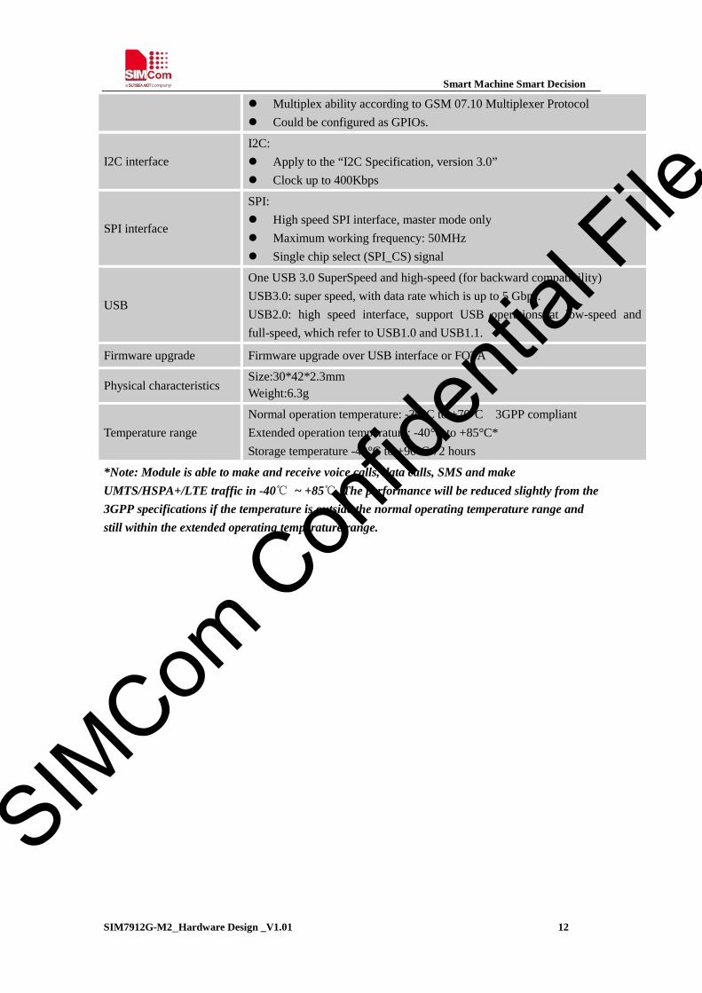
Multiplex ability according to GSM 07.10 Multiplexer Protocol Could be configured as GPIOs.
I2C interface I2C: Apply to the “I2C Specification, version 3.0” Clock up to 400Kbps
SPI interface
SPI: High speed SPI interface, master mode only Maximum working frequency: 50MHz Single chip select (SPI_CS) signal
USB
One USB 3.0 SuperSpeed and high-speed (for backward compatibility) USB3.0: super speed, with data rate which is up to 5 Gbps. USB2.0: high speed interface, support USB operations at low-speed and full-speed, which refer to USB1.0 and USB1.1.
Firmware upgrade Firmware upgrade over USB interface or FOTA
Physical characteristics Size:30*42*2.3mm Weight:6.3g
Temperature range Normal operation temperature: -30°C to +70°C 3GPP compliant Extended operation temperature: -40°C to +85°C* Storage temperature -40°C to +90°C 72 hours
*Note: Module is able to make and receive voice calls, data calls, SMS and make UMTS/HSPA+/LTE traffic in -40 ~ +85. The performance will be reduced slightly from the 3GPP specifications if the temperature is outside the normal operating temperature range and still within the extended operating temperature range.
SIMCom
Con
fiden
tial F
ile

Smart Machine Smart Decision
SIM7912G-M2_Hardware Design _V1.01 13
2 Package Information
2.1 Pin Assignment Overview
All functions of the M.2 card will be provided through 75 (including 8 notch pins) pads that will be connected to the customers’ platform. The following table is the high-level view of the pin assignment of the card. Table 3: Pin map
CONFIG_2 75
74 VBAT GND 73
72 VBAT GND 71
70 VBAT CONFIG_1 69
68 WLAN_PWR_EN
(1.8V) RESET#(1.8V) 67
66 SIM Detect
(1.8V) ANTCTL3(1.8V) 65
64 COEX_RX
(1.8V) ANTCTL2(1.8V) 63
62 COEX_TX
(1.8V) ANTCTL1(1.8V) 61
60 UART_TX/SPI_MOSI
(1.8V) ANTCTL0(1.8V) 59
58 UART_RX/SPI_MISO
(1.8V) GND 57
56 I2S_MCLK/ SI_RST_N
(1.8V) REFCLKP 55
54 PEWAKE#
(1.8V) REFCLKN 53
52 CLKREQ#
(1.8V) GND 51
50 PERST# (1.8V)
PERp0 49 48
GPIO4/WL_SLP_CLK (1.8V)
PERn0 47 46
GPIO3/GP_CLK/ SI_INT_N (1.8V)
GND 45 44
GPIO2/WLAN_EN (1.8V)
PETp0 43 42 I2C_SDA/UART_CTS/SPI_CS
SIMCom
Con
fiden
tial F
ile

Smart Machine Smart Decision
SIM7912G-M2_Hardware Design _V1.01 14
(1.8V) PETn0 41
40 I2C_SCL/UART_RTS/SPI_CLK
(1.8V) GND 39
38 BT_EN (1.8V)
USB3.0-Rx+ 37 36 UIM-PWR
USB3.0-Rx‐ 35 34 UIM-DATA
GND 33 32 UIM-CLK
USB3.0-Tx+ 31 30 UIM-RESET
USB3.0-Tx‐ 29 28 I2S_CLK (1.8V)
GND 27 26
W_DISABLE2# (3.3/1.8V) GPIO_12 - DPR/DPR
(1.8V) 25
24 I2S_DOUT
(1.8V) GPIO_11 - WoWWAN#/ WoWWAN# (1.8V)
23 22
I2S_DIN (1.8V)
CONFIG_0 21 20 I2S_WA (1.8V)
Notch Notch
Notch Notch
Notch Notch
Notch Notch
GND 11 10
LED1# (3.3V OD)
USB D- 9 8
W_DISABLE1# (3.3/1.8V)
USB D+ 7 6
FUL_CARD_POWER_OFF# (3.3/1.8V)
GND 5 4 VBAT
GND 3 2 VBAT
CONFIG_3 1
SIMCom
Con
fiden
tial F
ile

Smart Machine Smart Decision
SIM7912G-M2_Hardware Design _V1.01 15
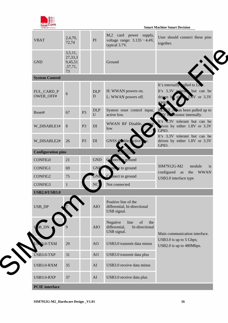
2.2 Pin Description
Table 4: IO parameters definition
Pin type Description
PI Power input PO Power output AI Analog input AIO Analog input/output DIO Bidirectional digital input /output DI Digital input DO Digital output DOH Digital output with high level DOL Digital output with low level PU Pull up PD Pull down OD Open Drain OC Open collector Table 5: IO parameters definition
Table 6: Pin description
Pin name Pin No.
Electrical Description Description Comment
Power supply
Voltage domain Parameter Min Typ Max
P3
VDD_P3=1.8V VOH High level output 1.35V - 1.8V VOL Low level output 0V - 0.45V VIH High level input 1.2V 1.8V 2.1V VIL Low level input -0.3V - 0.6V Rp Pull up/down resistor 80K ohm - 240K ohm
P4
VDD_P4=1.8V VOH High level output 1.44V - 1.8V VOL Low level output 0V - 0.4V VIH High level input 1.26V 1.8V 2.1V VIL Low level input -0.3V - 0.36V Rp Pull up/down resistor 360K ohm - VDD_P4=2.85V VOH High level output 2.28V - 2.85V VOL Low level output 0V - 0.4V VIH High level input 2.0V - 3.15V VIL Low level input -0.3V - 0.57V Rp Pull up/down resistor 285K ohm SIM
Com C
onfid
entia
l File
Smart Machine Smart Decision
SIM7912G-M2_Hardware Design _V1.01 16
VBAT 2,4,70,72,74 PI
M,2 card power supply, voltage range: 3.135~4.4V, typical 3.7V.
User should connect these pins together.
GND
3,5,11,27,33,39,45,51,57,71,73
Ground
System Control
FUL_CARD_POWER_OFF# 6 DI,P
D H: WWAN powers on. L: WWAN powers off.
It’s internally pulled to Low. It’s 3.3V tolerant but can be driven by either 1.8V or 3.3V GPIO.
Reset# 67 P3 DI,PU
System reset control input, active low.
RESET_N has been pulled up to 1.8V via resistor internally.
W_DISABLE1# 8 P3 DI WWAN RF Disable, active low
It’s 3.3V tolerant but can be driven by either 1.8V or 3.3V GPIO.
W_DISABLE2# 26 P3 DI GNSS disable, active low. It’s 3.3V tolerant but can be driven by either 1.8V or 3.3V GPIO.
Configuration pins
CONFIG0 21 GND Connect to ground SIM7912G-M2 module is configured as the WWAN USB3.0 interface type
CONFIG1 69 GND Connect to ground
CONFIG2 75 GND Connect to ground
CONFIG3 1 NC Not connected
USB2.0/USB3.0
USB_DP 7 AIO Positive line of the differential, bi-directional USB signal.
Main communication interface. USB3.0 is up to 5 Gbps; USB2.0 is up to 480Mbps.
USB_DN 9 AIO Negative line of the differential, bi-directional USB signal.
USB3.0-TXM 29 AO USB3.0 transmit data minus
USB3.0-TXP 31 AO USB3.0 transmit data plus
USB3.0-RXM 35 AI USB3.0 receive data minus
USB3.0-RXP 37 AI USB3.0 receive data plus
PCIE interface
SIMCom
Con
fiden
tial F
ile

Smart Machine Smart Decision
SIM7912G-M2_Hardware Design _V1.01 17
PETn0 41 AO PCIe TX Differential signals Negative
Support PCIe GEN 2.0, up to 5Gbps data rate. If unused, please keep them open.
PETp0 43 AO PCIe TX Differential signals Positive
PERn0 47 AI PCIe RX Differential signals Negative
PERp0 49 AI PCIe RX Differential signals Positive
REFCLKN 53 AIO PCIe Reference Clock signal Negative
REFCLKP 55 AIO PCIe Reference Clock signal Positive
PCIE assistant interface
PERST# 50 P3 DI Asserted to reset module PCIe interface default. Active low.
If unused, please keep them open.
CLKREQ# 52 P3 DIO
PCIe clock request. Open drain output requires external 100K resistor to 1.8V power source. Active low.
PEWAKE# 54 P3 DO
Asserted to wake up system. Open drain output requires external 100K resistor to 1.8V power source. Active low.
USIM interface
UIM-PWR 36 P4 PO
Power output for UIM card, the voltage depends on the UIM card type. Its output current is up to 50mA.
All lines of UIM interface should be protected against ESD.
UIM-DATA 34 P4 DIO
UIM Card data I/O, which has been pulled up via a 10KR resistor to UIM_PWR internally. Do not pull it up or down externally.
UIM-CLK 32 P4 DO UIM clock output
UIM-RESET 30 P4 DO UIM Reset output
SIM1_DETECT 66 P3 DI
UIM card detecting input signal which has been pulled up via a 10KR resistor to VDD_P3 internally.
ANTCTL signals
ANTCTL0 59 P3 DO Tunable ANT CTRL0 These signals are used for Antenna Control and should be
SIMCom
Con
fiden
tial F
ile

Smart Machine Smart Decision
SIM7912G-M2_Hardware Design _V1.01 18
ANTCTL1 61 P3 DO Tunable ANT CTRL1 routed to the appropriate Antenna Control Circuitry on the platform. These signals are 1.8V voltage domain. If unused, please keep them open.
ANTCTL2 63 P3 DO Tunable ANT CTRL2
ANTCTL3 65 P3 DO Tunable ANT CTRL3
WLAN control interface
COEX_RX 64 P3 DI
Wireless coexistence between WWAN and WiFi/BT modules, based on BT-SIG coexistence protocol.
DO NOT PULL UP COEX_TX (PIN 62) DURING NORMAL POWER UP! These signals are 1.8V voltage domain. If unused, keep them open.
COEX_TX 62 P3 DO
Wireless coexistence between WWAN and WiFi/BT modules, based on BT-SIG coexistence protocol.
WLAN_EN 44 P3 DO WLAN function enable
BT_EN 38 P3 DO Bluetooth function enable
WL_SLP_CLK 48 P3 DO WLAN sleep clock output
WL_PWR_EN 68 P3 DO WLAN power enable
Audio interface AUDIO_0: PCM_SYNC/ I2S_WA
20 P3 DO PCM synchronous signal ; I2S word select
These signals are 1.8V voltage domain. If unused, keep them open.
AUDIO_1: PCM_IN/ I2S_DIN
22 P3 DI PCM data input; I2S data input
AUDIO_2: PCM_OUT/ I2S_DOUT
24 P3 DO PCM data output; I2S data output
AUDIO_3: PCM_CLK I2S_CLK
28 P3 DO PCM clock output I2S clock output
I2S_MCLK/ SI_RST_N
56 P3 DO I2S system main clock/ SLIC reset output
Multiplex interface
I2C_SCL/ SPI_CLK/ UART_RTS
40 P3 DO I2C bus clock signal(default) SPI bus clock signal; UART request to send
These signals are 1.8V voltage domain. External pull-up resisters (2.2K recommended) are needed when the I2C interface is used. If unused, keep them open.
I2C_SDA/ SPI_CS/
42 P3 DIO I2C bus data signal(default); SPI chip select;
SIMCom
Con
fiden
tial F
ile

Smart Machine Smart Decision
SIM7912G-M2_Hardware Design _V1.01 19
UART_CTS UART clear to send
UART_RX/ SPI_MISO
58 P3 DI UART receive data(default) Master input slaver output
UART_TX/ SPI_MOSI
60 P3 DO UART transmit data(default) Master output slaver input
Other pins
LED#1 10 P3 OC
It is an open collector, active low signal, used to allow the M.2 card to provide status indicators via LED devices that will be provided by the system.
These signals are open-collector output. If unused, keep them open.
WAKE_ON_WWAN
23 P3 OC WWAN to wake up the host. It is open collector and active low.
DPR 25 P3 DI
Hardware Pin for BodySAR Detection, active low. H: Max transmitting power will not be reduced (default) L: Max transmitting power will be reduced
These signals are 1.8V voltage domain. If unused, keep them open.
GP_CLK/ SI_INT_N 46 P3 DO/
DI General purpose clock output/ SLIC interrupt input
Notch
Notch 12 Notch
Notch 13 Notch
Notch 14 Notch
Notch 15 Notch
Notch 16 Notch
Notch 17 Notch
Notch 18 Notch
Notch 19 Notch
SIMCom
Con
fiden
tial F
ile

Smart Machine Smart Decision
SIM7912G-M2_Hardware Design _V1.01 20
2.3 Mechanical Information
The following figure shows the package outline drawing of the M.2 card.
Figure 2: pin out diagram
2.4 Package Dimensions
Figure 3: Dimensions of SIM7912G-M2 (Unit: mm)
SIMCom
Con
fiden
tial F
ile

Smart Machine Smart Decision
SIM7912G-M2_Hardware Design _V1.01 21
3 Interface Application
3.1 Power Supply
The recommended power supply of SIM7912G-M2 is 3.7V and the voltage ranges from 3.135 V to 4.4 V. The SIM7912G-M2 has 5 power pins and 11 Ground pins, to ensure the SIM7912G-M2 card works normally, all the pins must be connected. The connector pin is defined to support 500mA current per pin continuously. Table 7: VBAT pins electronic characteristic
Symbol Description Min. Typ. Max. Unit VBAT Module power voltage 3.135 3.7 4.4 V
IVBAT(peak) Module power peak current in normal mode. - - 1 A
IVBAT(power-off) Module power current in power off mode. - 7 - uA
3.1.1 Power Supply Design Guide
Make sure that the voltage on the VBAT pins will never drop below 3.135V, even during a transmit event, when current consumption may rise up to 1.0A. If the voltage drops below 3.135V, the module will be powered off automatically. Note: Be sure the power supply for VBAT pins can support more than1.0A, using a total of more than 100uF capacitors is recommended, in order to avoid the voltage drop to lower than 3.135V. Some multi-layer ceramic chip (MLCC) capacitors (0.1/1uF) with low ESR in high frequency band can be used for EMC. These capacitors should be put as close as possible to VBAT pads. Also, users should keep VBAT trace on circuit board wider than 1.0 mm to minimize PCB trace impedance. The following figure shows the recommended circuit.
2
GNDGND
SIM7912G-M2
Cc
FB101
TVS
10uF
VBAT
Ca100uF
VBAT4707274 Cb
100nF
Cc33pF
VBAT
VBAT
VBAT
VBAT
Figure 4: Power supply application circuit
Note: The test condition: The voltage of power supply for VBAT is 3.7V, Ca is 100 µF tantalum capacitor (ESR=0.7Ω). In addition, in order to guard for over voltage protection, it is suggested to use a TVS diode to protect the M.2 card.
SIMCom
Con
fiden
tial F
ile

Smart Machine Smart Decision
SIM7912G-M2_Hardware Design _V1.01 22
Table 8: Recommended TVS diode list No. Manufacturer Part Number VRWM Package
1 JCET ESDBW5V0A1 5V DFN1006-2L
2 WAYON WS05DPF-B 5V DFN1006-2L
3 WILL ESD5611N 5V DFN1006-2L
4 WILL ESD56151W05 5V SOD-323
3.1.2 Recommended Power Supply Circuit
It is recommended that a switching mode power supply or a linear regulator power supply is used. It is important to make sure that all the components used in the power supply circuit can resist the current which could be more than 1A. The following figure shows the linear regulator reference circuit with 5V input and 3.7V output.
Vin Vout
GN
D
FB
3
+PWR_CTRL
R102
R101
VBAT
20K(1%)
10K(1%)
+
U101 MIC29302
5
4
1
2
C101 C102100uF 1uF
DC INPUT
R103470R
On/Off
FUSE
C103
330uF
C104
100nF
Figure 5: Linear regulator reference circuit
If there is a high dropout between input and VBAT, or the efficiency is extremely important, then a switching mode power supply will be preferable. The following figure shows the switching mode power supply reference circuit with 12V input and 3.7V output.
FUSEVin Vout
FB
U1011 2
3
45
LM2596-ADJ
+100uH
MBR360
L101
C101 +C102D102 C103
R102
R101
FB101
330uF
VBAT
20K(1%)
10K(1%)
100uF 1uFC104
100nF
270 ohm@100Mhz
DC INPUT
PWR_CTRL
GN
DOn/Off
Figure 6: Switching mode power supply reference circuit
Note: The Switching Mode power supply solution for VBAT must be chosen carefully against Electro Magnetic Interference and ripple current from depraving RF performance.
3.1.3 Voltage Monitor
To monitor the VBAT voltage, the AT command “AT+CBC” can be used.
SIMCom
Con
fiden
tial F
ile

Smart Machine Smart Decision
SIM7912G-M2_Hardware Design _V1.01 23
Note: For more details about voltage monitor commands, please refer to Document [1].
3.2 FUL_CARD_POWER_OFF#
Module can be powered on by pulling the FUL_CARD_POWER_OFF# pin, which is 3.3V tolerant,up to high level through GPIO. FUL_CARD_POWER_OFF# signal is an active low input signal and will turn the module on when asserted high (≥1.7 V) and will force the module to shut down when asserted low (≤0.2 V). This pin is 3.3V tolerant and can be driven by either 1.8V or 3.3V GPIO and has been pulled down internal.
Turn ON / OFF SIM7912G-M2
FUL_CARD_POWER_OFF#
CPU
GPIO(1.8V/3.3V
)
Figure 7: Reference power on/off circuit
Note: Module could be automatically power on by connecting FUL_CARD_POWER_OFF# pin to 3V3 via 0R resistor directly.
3.2.1 Power on
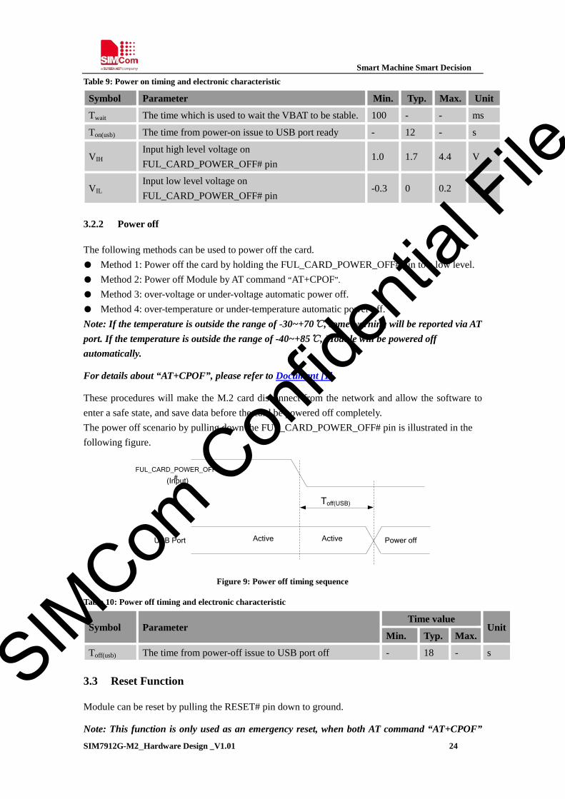
The power-on scenarios are illustrated in the following figure.
RESET#
(Input)
Twait
VBAT
FUL_CARD_POWER_OFF#
(Input)
USB Port Undefined Active
Ton(usb)
Power off
Figure 8: Power on timing sequence
SIMCom
Con
fiden
tial F
ile
Smart Machine Smart Decision
SIM7912G-M2_Hardware Design _V1.01 24
Table 9: Power on timing and electronic characteristic Symbol Parameter Min. Typ. Max. Unit
Twait The time which is used to wait the VBAT to be stable. 100 - - ms
Ton(usb) The time from power-on issue to USB port ready - 12 - s
VIH Input high level voltage on FUL_CARD_POWER_OFF# pin
1.0 1.7 4.4 V
VIL Input low level voltage on FUL_CARD_POWER_OFF# pin
-0.3 0 0.2 V
3.2.2 Power off
The following methods can be used to power off the card. Method 1: Power off the card by holding the FUL_CARD_POWER_OFF# pin to a low level. Method 2: Power off Module by AT command “AT+CPOF”. Method 3: over-voltage or under-voltage automatic power off. Method 4: over-temperature or under-temperature automatic power off. Note: If the temperature is outside the range of -30~+70, some warning will be reported via AT port. If the temperature is outside the range of -40~+85, Module will be powered off automatically.
For details about “AT+CPOF”, please refer to Document [1].
These procedures will make the M.2 card disconnect from the network and allow the software to enter a safe state, and save data before the card be powered off completely. The power off scenario by pulling down the FUL_CARD_POWER_OFF# pin is illustrated in the following figure.
Toff(USB)
(Input)
USB Port Power offActive
FUL_CARD_POWER_OFF#
Active
Figure 9: Power off timing sequence
Table 10: Power off timing and electronic characteristic
Symbol Parameter Time value
Unit Min. Typ. Max.
Toff(usb) The time from power-off issue to USB port off - 18 - s
3.3 Reset Function
Module can be reset by pulling the RESET# pin down to ground.
Note: This function is only used as an emergency reset, when both AT command “AT+CPOF”
SIMCom
Con
fiden
tial F
ile

Smart Machine Smart Decision
SIM7912G-M2_Hardware Design _V1.01 25
and the FUL_CARD_POWER_OFF# pin have lost efficacy. The RESET# pin has been pulled up with a resistor to 1.8V internally, so it does not need to be pulled up externally. It is strongly recommended to put a100pF capacitor and an ESD protection diode close to the RESET# pin. Please refer to the following figure for the recommended reference circuit.
4.7K
47K
Reset Impulse RESET# Reset Logic
R
1.8V
MODULE
1K
100pF
Treset
Figure 10: Reference reset circuit
Table 11: RESET pin electronic characteristic
Symbol Description Min. Typ. Max. Unit
Treset The active low level impulse time on RESET_N pin to reset Module
100 150 500 ms
VIH Input high level voltage 1.17 1.8 2.1 V
VIL Input low level voltage -0.3 0 0.8 V
3.4 UART interface
Module provides a 2-wire UART (universal asynchronous serial transmission) interface as DCE (Data Communication Equipment). AT commands and data transmission can be performed through UART interface. The following figures show the reference design.
MODULE(DCE)
HOST(DTE)
UARTUART
TXDRXD
TXDRXD
Figure 11: UART modem
The Module UART is 1.8V voltage interface. If user’s UART application circuit is 3.3V voltage interface, the level shifter circuits should be used for voltage matching. The TXB0102RGYR provided by Texas Instruments is recommended. The following figure shows the voltage matching reference design.
SIMCom
Con
fiden
tial F
ile

Smart Machine Smart Decision
SIM7912G-M2_Hardware Design _V1.01 26
TXDRXD
A1A2
SIM7912GTXB0102RGY
RUART port
B1B2
VCCAOE
VDD_1V8 or External 1V8
100nF
3.3V
100nFVCCB
GND
TXD_3.3VRXD_3.3V
Figure 12: Reference circuit of level shift
Note: Module supports the following baud rates: 300, 600, 1200, 2400, 4800, 9600, 19200, 38400, 57600, 115200, 230400, 460800, 921600. The default band rate is 115200bps.
3.5 I2C Interface
Module provides an I2C interface compatible with I2C specification, version 3.0, with clock rate up to 400 kbps. Its operation voltage is 1.8V. The following figure shows the I2C bus reference design.
Module
I2C_SDA
I2C device
SDA
GNDGND
I2C_SCL SCL
VDD_1V8
2.2K
2.2K
Figure 13: I2C reference circuit
Note:SDA and SCL have no pull-up resistors in Module. So, 2 external pull up resistors are necessary in application circuit. For more details about AT commands please refer to document [1].
3.6 SPI Interface
SIM7912 provides a multiplex SPI interface as a master only. It provides a duplex, synchronous, serial communication link with peripheral devices. Its operation voltage is 1.8V, with clock rates up to 50 MHz The SPI interface could also be configured as UART, I2C or GPIOs, which could refer to the Table below.
SIMCom
Con
fiden
tial F
ile

Smart Machine Smart Decision
SIM7912G-M2_Hardware Design _V1.01 27
Table 12: SPI interface configure
PIN Mode 0(Default ) Mode 1 Mode 2 Mode 3 Mode 4 Mode 5
UART +I2C SPI mode BT_UART mode
UART +GPIO
I2C+GPIO GPIOs
60 UART_TX SPI_MOSI BT_TXD UART_TX GPIO GPIO
58 UART_RX SPI_MISO BT_RXD UART_RX GPIO GPIO
42 I2C_SDA SPI_CS BT_CTS GPIO I2C_SDA GPIO
40 I2C_SCL SPI_CLK BT_RTS GPIO I2C_SCL GPIO
Note:For more details of the AT commands about the SPI, please refer to document [1].
3.7 WoWWAN#
The WoWWAN# pin is an open collector signal which can be used as an interrupt signal to the host. Normally it will keep high logic level until certain conditions such as receiving SMS, voice call (CSD, video) or URC reporting, then WoWWAN# will change to low logic level to inform the host (client PC), the pulse time is 1 second.
HIGH
LOW
1s
WoWWAN#
Figure 14: WOWWAN# behaviour(SMS and URC report)
WAKE_ON_WWAN Reference circuit is recommended in the following figure.
SIM7912G-M2
VCC From Host
10 ~100K
HOSTInterrupt input
BB Chip
WoWWAN#
4.7K
47K
Figure 15: WOWWAN# reference circuit
3.8 USB3.0 Interface
The module support one integrated USB interface which complies with the USB 3.0 specifications and supports super speed up to 5Gbps. The USB interface is used for AT command communication, data transmission, GNSS NMEA output, software debugging and voice over USB.
SIMCom
Con
fiden
tial F
ile

Smart Machine Smart Decision
SIM7912G-M2_Hardware Design _V1.01 28
Note:The USB3.0-Tx+ and USB3.0-Tx- should be routed together and the nets must be traced by 90Ohm+/-10% differential impedance. The same treatment should be needed for the routing of USB3.0-RX+ and USB3.0-RX-.
3.9 USB2.0 Interface
The Module implements a USB interface compliant with the USB2.0 specification. The module supports three USB speeds: low-speed (1.5Mbps), full-speed (12Mbps) and high-speed (480Mbps). But the OTG function and USB charging function are not supported.
Note:The USB_DN and USB_DP nets must be traced by 90Ohm+/-10% differential impedance.
Module is used as a USB device by default. Module supports the USB suspend and resume mechanism which can reduce power consumption. If there is no data transmission on the USB bus, Module will enter suspend mode automatically, and will be resumed by some events such as voice call, receiving SMS, etc. The reference schematic is as following:
SIM7912Slave
USBHost
USB_DP
GNDGND
≤3pF
USB_DN
USB D+
USB D-
D2 D1
USB3.0-Rx+
USB3.0-Rx-
USB3.0-Tx+
USB3.0-Tx-
SS-Rx+
SS-Rx-
SS-Tx+
SS-Tx-
D6 D5
≤0.5pF
D4 D3
5Gbps
5Gbps
480Mbps
Figure 16: USB reference circuit
Because of the high bit rate on USB bus, more attention should be paid to the influence of the junction capacitance of the ESD component on USB data lines. Typically, for the USB2.0 signals (USB D- and USB D+), the capacitance should not be more than 3pF. It is recommended to use an ESD protection component such as ESD9M5.0ST5G provided by On Semiconductor (www.onsemi.com ). However, for the USB3.0 signals (USB3.0-Tx and USB3.0-Rx), the capacitance should not be more than 0.5pF. It is recommended to use an ESD protection component such as ESD9L5.0ST5G provided by On Semiconductor (www.onsemi.com ).
SIMCom
Con
fiden
tial F
ile

Smart Machine Smart Decision
SIM7912G-M2_Hardware Design _V1.01 29
3.10 UIM Interface
Module supports both 1.8V and 3.0V UIM Cards. Table 13: UIM electronic characteristic in 1.8V mode (UIM-PWR=1.8V)
Symbol Parameter Min. Typ. Max. Unit
UIM-PWR LDO power output voltage 1.75 1.8 1.95 V
VIH High-level input voltage 0.65*UIM-PWR - UIM-PWR +0.3 V
VIL Low-level input voltage -0.3 0 0.35*UIM-PWR V
VOH High-level output voltage UIM-PWR -0.45 - UIM-PWR V
VOL Low-level output voltage 0 0 0.45 V
Table 14: UIM electronic characteristic 3.0V mode (UIM-PWR=2.85V)
Symbol Parameter Min. Typ. Max. Unit
UIM-PWR LDO power output voltage 2.75 2.85 3.05 V
VIH High-level input voltage 0.65*UIM-PWR - UIM-PWR +0.3 V
VIL Low-level input voltage -0.3 0 0.25*UIM-PWR V
VOH High-level output voltage UIM-PWR -0.45 - UIM-PWR V
VOL Low-level output voltage 0 0 0.45 V
3.10.1 USIM Application Guide
It is recommended to use an ESD protection component such as ESDA6V1-5W6 produced by ST (www.st.com ) or SMF12C produced by ON SEMI (www.onsemi.com ). Note that the USIM peripheral circuit should be close to the USIM card socket. The following figure shows the 6-pin SIM card holder reference circuit.
SIM7912G-M2
TVS
UIM-PWR
UIM-CLK
UIM-DATA
UIM-RESET VCC GNDRST VPPCLK I/O
22Ω
100nF
C707 10M006 512
USIM Socket
0Ω
22Ω
22pF(NC)
22pF(NC)
22pF(NC)
Figure 17: USIM interface reference circuit
The SIM Detect pin is used for detection of the UIM card hot plug in. User can select the 8-pin UIM card holder to implement UIM card detection function.
SIMCom
Con
fiden
tial F
ile

Smart Machine Smart Decision
SIM7912G-M2_Hardware Design _V1.01 30
The following figure shows the 8-pin SIM card holder reference circuit.
SIM7912G-M2
UIM-PWR
UIM-CLK
UIM-DATA
UIM-RESET
SIM Detect PRESENCE
100nF
MOLEX - 91228
UIM Card
VCC GND
RST VPP
CLK I/O
22pF(NC)
TVS1
Deserved
22R
0R
22R
22R
22pF(NC)
22pF(NC)
Figure 18: UIM interface reference circuit with UIM_DET
If the UIM card detection function is not used, user can keep the SIM Detect pin open. SIM card circuit is susceptible, the interference may cause the SIM card failures or some other situations, so it is strongly recommended to follow these guidelines while designing: Make sure that the SIM card holder should be far away from the antenna while in PCB
layout. SIM traces should keep away from RF lines, VBAT and high-speed signal lines. The traces should be as short as possible. Keep SIM holder’s GND connect to main ground directly. Shielding the SIM card signal by ground. Recommended to place a 0.1~1uF capacitor on UIM-PWR line and keep close to the
holder. The rise/fall time of UIM-CLK should not be more than 40ns. Add some TVS and the parasitic capacitance should not exceed 60pF.
3.11 I2S Interface
Module provides an I2S interface for external codec, which comply with the requirements in the Phillips I2S Bus Specifications Table 15: I2S format
Note: For more details about I2S AT commands, please refer to document [1].
3.11.1 I2S timing
Module supports 48 KHz I2S sampling rate and 32 bit coding signal (16 bit word length), the
Characteristics Specification
Line Interface Format Linear(Fixed)
Data length 16bits(Fixed)
I2S Clock/Sync Source Master Mode(Fixed)
I2S Clock Rate 1.536 MHz (Default)
I2S MCLK rate 12.288MHz (Default)
Data Ordering MSB SIMCom
Con
fiden
tial F
ile

Smart Machine Smart Decision
SIM7912G-M2_Hardware Design _V1.01 31
timing diagram is showed as following:
Figure 19: I2S timing
Table 16: I2S timing parameters
3.11.2 I2S reference circuit
The following figure shows the external codec reference design.
Signal Parameter Description Min. Typ. Max. Unit
I2S_MCLK
Frequency Frequency – 12.288 12.288 MHz
T Clock period 81.380 81.380 – ns
t(HC) Clock high 0.45T – 0.55T ns
t(LC) Clock low 0.45T – 0.55T ns
I2S_CLK
Frequency Frequency 8 48 48 KHz
T Clock period 20.83 20.83 125 us
t(HC) Clock high 0.45T – 0.55T ns
t(LC) Clock low 0.45T – 0.55T ns
I2S_WS
t(sr) DIN/DOUT and WS input setup time
16.276 – – ns
t(hr) DIN/DOUT and WS input hold time
0 – – ns
t(dtr) DIN/DOUT and WS output delay
– – 65.10 ns
t(htr) DIN/DOUT and WS output hold time
0 – – ns
SIMCom
Con
fiden
tial F
ile

Smart Machine Smart Decision
SIM7912G-M2_Hardware Design _V1.01 32
SIM7912G-M2
I2S_DIN
I2S_WSI2S_CLK
I2S_DOUT
33pF
ADCOUT
FSBCLK
DACIN
MCLK
VDD_1V8
2.2K2.2K
SCLKSDIO
I2C1_SCLI2C1_SDA
VDDA
VDDSPK
VDDD
3.3V 3.3V VDD_1V8
MIC+MIC-
MICBIAS
MOUT
MIC
ReceiverNAU88U10
2.2K
2.2K
1uF1uF
47uF
47uF
I2S_MCLK
Figure 20: Audio codec reference circuit
3.12 DPR*
DPR (Dynamic Power Reduction) signal is used by SIM7912G-M2 to assist in meeting regulatory SAR (Specific Absorption Rate) requirements for RF exposure. The signal is provided by a host system proximity sensor to the wireless device to provide an input trigger causing a reduction in the radio transmit output power. User can use AT command to active this function, if do not need this function, this pin can be keep floating. Table 17: DPR interface
Pin no Pin Name Pin status Function
25 DPR
Low Max transmitting power will be reduced
High Max transmitting power will not be reduced (default)
Floating Max transmitting power will not be reduced Note:* means the DRP function is under developing.
3.13 CONFIG Pins
These signals provide the means to indicate the specific configuration of the module. SIM7912G-M2 is configured as WWAN-USB3.0. Table 18: CONFIG Pins
Pin no Pin Name Description
21 CONFIG_0 Connected to GND internally.
69 CONFIG_1 Connected to GND internally.
75 CONFIG_2 Connected to GND internally.
1 CONFIG_3 No Connect internally.
In the M.2 specification, the 4 pins are defined as below:
SIMCom
Con
fiden
tial F
ile

Smart Machine Smart Decision
SIM7912G-M2_Hardware Design _V1.01 33
Table 19: Config interface
Config_0 (Pin 21)
Config_1 (Pin 69)
Config_2 (Pin 75)
Config_3 (Pin 1)
Module type and Main host interface
Port Configuration
GND GND GND GND SSD – SATA N/A
GND NC GND GND SSD – PCIe N/A
GND GND NC GND WWAN – PCIe 0
GND NC NC GND WWAN – PCIe 1
GND GND GND NC WWAN – USB 3.0 0
GND NC GND NC WWAN – USB 3.0 1
GND GND NC NC WWAN – USB 3.0 2
GND NC NC NC WWAN – USB 3.0 3
NC GND GND GND WWAN – SSIC 0
NC NC GND GND WWAN – SSIC 1
NC GND NC GND WWAN – SSIC 2
NC NC NC GND WWAN – SSIC 3
NC GND GND NC WWAN – PCIe 2
NC NC GND NC WWAN – PCIe 3
NC GND NC NC RFU N/A
NC NC NC NC No Module Present N/A
3.14 LED1#
LED1# is open collector output and is used to allow SIM7912G-M2 to provide network status via LED which will be provided by the host.
R
VCC
LED1#
SIM7912G-M2
BB Chip4.7K
47K
Figure 21: LED1# reference circuit
Note: The value of the resistor named “R” depends on the LED characteristic. The timing sequence is as followed:
SIMCom
Con
fiden
tial F
ile

Smart Machine Smart Decision
SIM7912G-M2_Hardware Design _V1.01 34
Table 20: LED1# pin status
NETLIGHT pin status Module status
Always On Searching Network; Call Connect(include VOLTE,SRLTE)
200ms ON, 200ms OFF Data Transmit; 4G registered;
800ms ON, 800ms OFF 3G registered network
OFF Power off ;Sleep
3.15 W_DISABLE1#
The W_DISABLE1# pin controls SIM7912G-M2 to enter or exit the flight mode, when the W_DISABLE1# signal is asserted to low level, all RF functions would be disabled. When the W_DISABLE1# signal is not asserted, the RF function will be active if it was not disabled by other means such as software. Its reference circuit is shown in the following figure.
SIM7912G-M2
47K
W_DISABLE1#
GPIO
4.7K
4.7K
Switch
1.8/3.3V
1.8V
Figure 22: Flight mode switch reference circuit
Flight Mode pin status as below: Table 21: FLIGHTMODE pin status
FLIGHTMODE pin status Module operation Input Low Level Flight Mode: RF is closed
Input High Level AT+CFUN=4: RF is closed AT+CFUN=1: RF is working
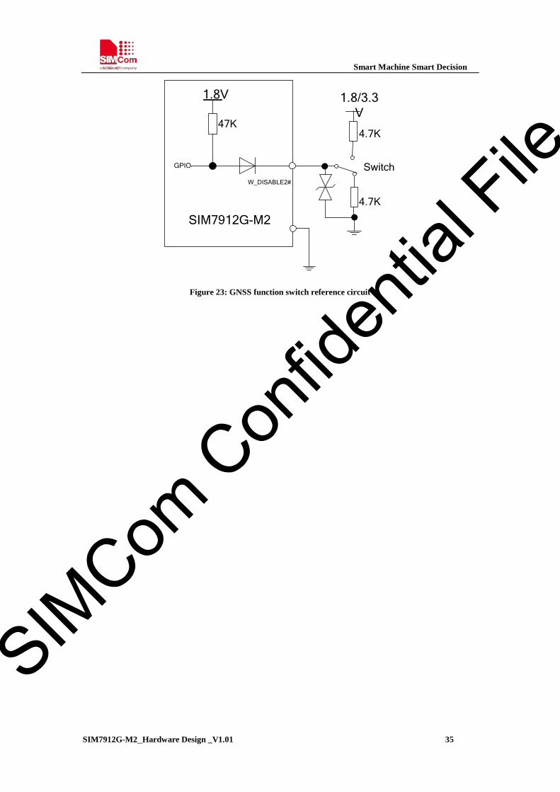
3.16 W_DISABLE2#
The W_DISABLE2# pin controls SIM7912G-M2 to enable or disable the GNSS function, when the W_DISABLE2# signal is asserted to low level, the GNSS function would be disabled. Its reference circuit is shown in the following figure.
SIMCom
Con
fiden
tial F
ile
Smart Machine Smart Decision
SIM7912G-M2_Hardware Design _V1.01 35
SIM7912G-M2
47K
W_DISABLE2#
GPIO
4.7K
4.7K
Switch
1.8/3.3V
1.8V
Figure 23: GNSS function switch reference circuit
SIMCom
Con
fiden
tial F
ile
Smart Machine Smart Decision
SIM7912G-M2_Hardware Design _V1.01 36
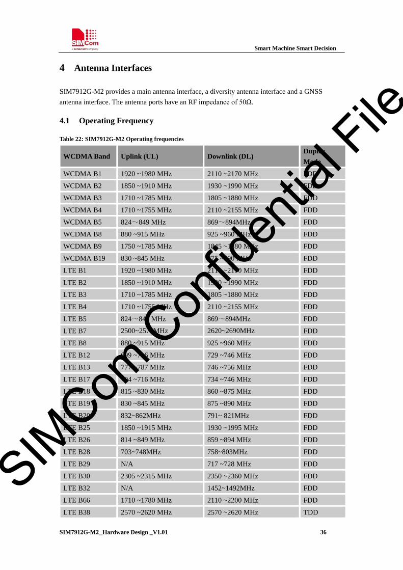
4 Antenna Interfaces
SIM7912G-M2 provides a main antenna interface, a diversity antenna interface and a GNSS antenna interface. The antenna ports have an RF impedance of 50Ω.
4.1 Operating Frequency
Table 22: SIM7912G-M2 Operating frequencies
WCDMA Band Uplink (UL) Downlink (DL) Duplex Mode
WCDMA B1 1920 ~1980 MHz 2110 ~2170 MHz FDD
WCDMA B2 1850 ~1910 MHz 1930 ~1990 MHz FDD
WCDMA B3 1710 ~1785 MHz 1805 ~1880 MHz FDD
WCDMA B4 1710 ~1755 MHz 2110 ~2155 MHz FDD
WCDMA B5 824~849 MHz 869~894MHz FDD
WCDMA B8 880 ~915 MHz 925 ~960 MHz FDD
WCDMA B9 1750 ~1785 MHz 1845 ~1880 MHz FDD
WCDMA B19 830 ~845 MHz 875 ~890 MHz FDD
LTE B1 1920 ~1980 MHz 2110 ~2170 MHz FDD
LTE B2 1850 ~1910 MHz 1930 ~1990 MHz FDD
LTE B3 1710 ~1785 MHz 1805 ~1880 MHz FDD
LTE B4 1710 ~1755 MHz 2110 ~2155 MHz FDD
LTE B5 824~849 MHz 869~894MHz FDD
LTE B7 2500~2570MHz 2620~2690MHz FDD
LTE B8 880 ~915 MHz 925 ~960 MHz FDD
LTE B12 699 ~716 MHz 729 ~746 MHz FDD
LTE B13 777 ~787 MHz 746 ~756 MHz FDD
LTE B17 704 ~716 MHz 734 ~746 MHz FDD
LTE B18 815 ~830 MHz 860 ~875 MHz FDD
LTE B19 830 ~845 MHz 875 ~890 MHz FDD
LTE B20 832~862MHz 791~ 821MHz FDD
LTE B25 1850 ~1915 MHz 1930 ~1995 MHz FDD
LTE B26 814 ~849 MHz 859 ~894 MHz FDD
LTE B28 703~748MHz 758~803MHz FDD
LTE B29 N/A 717 ~728 MHz FDD
LTE B30 2305 ~2315 MHz 2350 ~2360 MHz FDD
LTE B32 N/A 1452~1492MHz FDD
LTE B66 1710 ~1780 MHz 2110 ~2200 MHz FDD
LTE B38 2570 ~2620 MHz 2570 ~2620 MHz TDD
SIMCom
Con
fiden
tial F
ile

Smart Machine Smart Decision
SIM7912G-M2_Hardware Design _V1.01 37
LTE B39 1880 ~1920 MHz 1880 ~1920 MHz TDD
LTE B40 2300 ~2400 MHz 2300 ~2400 MHz TDD
LTE B41 2555 ~2655 MHz 2555 ~2655 MHz TDD
Note: LTE-FDD B29/B32 supports Rx only and is only for secondary component carrier.
4.2 GNSS Antenna Interface
The following table shows frequency specification of GNSS antenna interface. Table 23: GNSS frequencies
Type Frequecy
GPS/Galileo/QZSS 1575.42±1.023MHz
GLONASS 1597.5~1605.8MHz
BeiDou/Compass 1561.098±2.046MHz
4.3 Antenna Installation
4.3.1 Antenna Requirements
The following table shows the requirements on main antenna, Diversity antenna and GNSS antenna. Table 24:WCDMA/LTE antenna
Passive Recommended standard
Direction Omni directional
Gain > -3dBi (Avg)
Input impedance 50 Ω
Efficiency > 30 %
VSWR < 2
Cable insertion Loss <1GHz <1dB
Cable insertion Loss 1GHz~2.2GHz <1.5dB
Cable insertion Loss 2.3GHz~2.7GHz <2dB
Table 25:GNSS antenna
Passive Recommended standard
Frequency Range 1559~1609MHZ
Direction RHCP or liner, RHCP is the first choice
VSWR < 2
Passive antenna gain > 0 dBi
Active antenna NF < 1.5
Active antenna gain > 0 dBi
Active antenna Embedded LNA gain < 17 dB
SIMCom
Con
fiden
tial F
ile

Smart Machine Smart Decision
SIM7912G-M2_Hardware Design _V1.01 38
Note: It is recommended to use a passive GNSS antenna when LTE B13 is supported, as the use of active
antenna may generate harmonics which will affect the GNSS performance.
4.3.2 Recommended RF Connector for Antenna Installation
When choosing antennas, user should pay attentions to the connector on antenna which should match with the
connector on the module.
The standard 2x2 mm size RF receptacle connectors have been used on SIM7912G-M2. The dimension of the
connector on SIM7912G-M2 is 2.0*2.0*0.6mm, which is from Murata, and the Part Number is MM4829-2702B/
RA4/ RB0.
Shows the RF connector dimension in the following figure:
Figure 24: Antenna connector
The major specifications of the RF connector as below:
Table 26: the major specifications of the RF connector
Item Specification
Nominal Frequency Range DC to 6 GHz
Nominal Impedance 50Ω
Temperature Rating -40 to + 85
Initial Contact Resistance
(without conductor resistance)
Center contact 20.0mΩmax.
Outer contact 20.0mΩmax.
Voltage Standing Wave Ratio (V.S.W.R.)
Meet the requirements of
1.3max.(DC∼3GHz)
1.45max.(3GHz∼6GHz)
There are two kinds of coaxial cables mating the RF connector in the SIM7912G, SIMCom recommend use
Murata and SUZHOU KELI, and the Part Number is MXFR32HP1000 of the Murata and KLC-2058 of the
KELI.
SIMCom
Con
fiden
tial F
ile

Smart Machine Smart Decision
SIM7912G-M2_Hardware Design _V1.01 39
5 Electrical Specifications
5.1 Absolute maximum ratings
Absolute maximum rating for digital and analog pins of Module are listed in the following table: Table 27:Absolute maximum ratings
Parameter Min. Typ. Max. Unit
Voltage at VBAT pins -0.3 - 4.7 V
Voltage at digital pins (GPIO,I2C,UART, I2S) -0.3 - 2.1 V
Voltage at digital pins (UIM) -0.3 - 3.05 V
Voltage at FULCARD_POWER_OFF# -0.3 - 4.7
Voltage at RESET# -0.3 - 2.1
5.2 Operating conditions
Table 28: Recommended operating ratings
Parameter Min. Typ. Max. Unit Voltage at VBAT 3.135 3.7 4.4 V Table 29: 1.8V Digital I/O characteristics*
Parameter Description Min. Typ. Max. Unit
VIH High-level input voltage 1.17 1.8 2.1 V
VIL Low-level input voltage -0.3 0 0.63 V
VOH High-level output voltage 1.35 - 1.8 V
VOL Low-level output voltage 0 - 0.45 V
IOH High-level output current(no pull down resistor) - 2 - mA
IOL Low-level output current(no pull up resistor)
- -2 - mA
IIH Input high leakage current (no pull down resistor) - - 1 uA
IIL Input low leakage current(no pull up resistor) -1 - - uA
*Note: These parameters are for digital interface pins, such as UART, I2C, I2S, RESET#, ANTCTL, COEX and GPIOs (DPR, SIM DETECT).
SIMCom
Con
fiden
tial F
ile
Smart Machine Smart Decision
SIM7912G-M2_Hardware Design _V1.01 40
The operating temperature of Module is listed in the following table. Table 30:Operating temperature
Parameter Min. Typ. Max. Unit Normal operation temperature(3GPP compliant) -30 25 70 Extended operation temperature* -40 25 85 Storage temperature -40 25 90 *Note: Module is able to make and receive voice calls, data calls, SMS and make UMTX/LTE traffic in -40 ~ +85. The performance will be reduced slightly from the 3GPP specifications if the temperature is outside the normal operating temperature range and still within the extreme operating temperature range.
5.3 Operating Mode
5.3.1 Operating Mode Definition
The table below summarizes the various operating modes of Module product. Table 31: Operating mode Definition
Mode Function
Nor
mal
ope
ratio
n
UMTS/LTE Sleep
AT command “AT+CSCLK=1” can be used to set the module to a sleep mode. In this case, the current consumption of module will be reduced to a very low level and the module can still receive paging message and SMS.
UMTS/LTE Idle Software is active. Module is registered to the network, and the Module is ready to communicate.
UMTS/LTE Talk Connection between two subscribers is in progress. In this case, the power consumption depends on network settings such as DTX off/on, FR/EFR/HR, hopping sequences, and antenna.
UMTS/LTE Standby Module is ready for data transmission, but no data is currently sent or received. In this case, power consumption depends on network settings.
UMTS/LTE Data transmission
There is data transmission in progress. In this case, power consumption is related to network settings (e.g. power control level); uplink/downlink data rates, etc.
Minimum functionality mode
AT command “AT+CFUN=0” can be used to set the Module to a minimum functionality mode without removing the power supply. In this mode, the RF part of the Module will not work and the USIM card will not be accessible, but the serial port and USB port are still accessible. The power consumption in this mode is lower than normal mode.
Flight mode
AT command “AT+CFUN=4” or pulling down the W_disable1# pin can be used to set the Module to flight mode without removing the power supply. In this mode, the RF part of the Module will not work, but the serial port and USB port are still accessible. The power
SIMCom
Con
fiden
tial F
ile

Smart Machine Smart Decision
SIM7912G-M2_Hardware Design _V1.01 41
consumption in this mode is lower than normal mode.
Power off
Module will go into power off mode by sending the AT command “AT+CPOF” or pull down the FUL_CARD_POWER_OFF# pin, normally. In this mode the power management unit shuts down the power supply, and software is not active. The serial port and USB are is not accessible.
5.3.2 Sleep mode
In sleep mode, the current consumption of Module will be reduced to a very low level, and Module can still receive paging message and SMS. Several hardware and software conditions must be satisfied in order to let Module enter into sleep mode: 1. UART condition 2. USB condition 3. Software condition Note: Before designing, pay attention to how to realize sleeping/waking function.
5.3.3 Minimum functionality mode and Flight mode
Minimum functionality mode ceases a majority function of Module, thus minimizing the power consumption. This mode is set by the AT command which provides a choice of the functionality levels. AT+CFUN=0: Minimum functionality AT+CFUN=1: Full functionality (Default) AT+CFUN=4: Flight mode If Module has been set to minimum functionality mode, the RF function and UIM card function will be closed. In this case, the serial port and USB are still accessible, but RF function and UIM card will be unavailable. If Module has been set to flight mode, the RF function will be closed. In this case, the serial port and USB are still accessible, but RF function will be unavailable. When Module is in minimum functionality or flight mode, it can return to full functionality by the AT command “AT+CFUN=1”.
5.4 Current Consumption
The current consumption is listed in the table below.
SIMCom
Con
fiden
tial F
ile

Smart Machine Smart Decision
SIM7912G-M2_Hardware Design _V1.01 42
Table 32:Current consumption on VBAT Pins (VBAT=3.7V)
GNSS GNSS supply current (AT+CFUN=0, with USB connection)
@ -140dBm,Tracking Typical:52mA
UMTS sleep mode WCDMA supply current (GNSS off,without USB connection)
Sleep mode @DRX=2.56S Typical: 2.45mA
LTE sleep mode LTE FDD supply current (GNSS off,without USB connection)
Sleep mode Typical: 3.0mA
LTE TDD supply current (GNSS off,without USB connection)
Sleep mode Typical: 3.0mA
UMTS Talk WCDMA B1 @Power 23dBm Typical: 700mA
WCDMA B2 @Power 23dBm Typical: 700mA
WCDMA B3 @Power 23dBm Typical: 700mA
WCDMA B4 @Power 23dBm Typical: 750mA
WCDMA B5 @Power 23dBm Typical: 650mA
WCDMA B8 @Power 23dBm Typical: 700mA
WCDMA B9 @Power 23dBm Typical: 700mA
WCDMA B19 @Power 23dBm Typical: 650mA HSDPA data WCDMA B1 @Power 23dBm Typical: 700mA WCDMA B2 @Power 23dBm Typical: 700mA WCDMA B3 @Power 23dBm Typical: 700mA WCDMA B4 @Power 23dBm Typical: 750mA WCDMA B5 @Power 23dBm Typical: 650mA WCDMA B8 @Power 23dBm Typical: 700mA WCDMA B9 @Power 23dBm Typical: 700mA WCDMA B19 @Power 23dBm Typical: 650mA LTE data
LTE-FDD B1 @5MHz 22.8dBm Typical: 700mA @10MHz 23.0dBm Typical: 700mA @20MHz 23.9dBm Typical: 750mA
LTE-FDD B2 @5MHz 21.5dBm Typical: 700mA @10MHz 21.5dBm Typical: 700mA @20MHz 22.5dBm Typical: 700mA
LTE-FDD B3 @5MHz 22.5dBm Typical: 750mA @10MHz 22.5dBm Typical: 750mA @20MHz 23.5dBm Typical: 800mA
LTE-FDD B4 @5Mbps 21.5dBm Typical: 700mA
@10Mbps 21.5dBm Typical: 700mA
@20Mbps 22.5dBm Typical: 750mA
SIMCom
Con
fiden
tial F
ile

Smart Machine Smart Decision
SIM7912G-M2_Hardware Design _V1.01 43
LTE-FDD B5 @5Mbps 23.3dBm Typical: 700mA
@10Mbps 23.4dBm Typical: 700mA
@20Mbps 22.1dBm Typical: 700mA
LTE-FDD B7 @5Mbps 23.0dBm Typical: 700mA
@10Mbps 23.1dBm Typical: 700mA
@20Mbps 23.1dBm Typical: 800mA
LTE-FDD B8 @5Mbps 23.1dBm Typical: 750mA
@10Mbps 23.4dBm Typical: 750mA
LTE-FDD B12 @5Mbps 23.3dBm Typical: 700mA
@10Mbps 23.4dBm Typical: 750mA
LTE-FDD B13 @5Mbps 23.3dBm Typical: 750mA
@10Mbps 23.4dBm Typical: 750mA
LTE-FDD B17 @5Mbps 23.3dBm Typical: 700mA
@10Mbps 23.4dBm Typical: 700mA
LTE-FDD B18 @5Mbps 23.3dBm Typical: 750mA
@10Mbps 23.4dBm Typical: 750mA
@15Mbps 22.1dBm Typical: 700mA
LTE-FDD B19 @5Mbps 23.3dBm Typical: 750mA
@10Mbps 23.4dBm Typical: 750mA
@15Mbps 22.1dBm Typical: 700mA
LTE-FDD B20 @5Mbps 21.8dBm Typical: 750mA
@10Mbps 21.8dBm Typical: 750mA
@20Mbps 21.8dBm Typical: 750mA
LTE-FDD B25 @5Mbps 21.5dBm Typical: 700mA
@10Mbps 21.5dBm Typical: 700mA
@20Mbps 22.5dBm Typical: 700mA
LTE-FDD B26 @5Mbps 23.3dBm Typical: 700mA
@10Mbps 23.4dBm Typical: 700mA
@20Mbps 22.1dBm Typical: 650mA
LTE-FDD B28 @5Mbps 21.8dBm Typical: 700mA
@10Mbps 21.8dBm Typical: 700mA
@20Mbps 21.8dBm Typical: 700mA
LTE-FDD B29 N/A
LTE-FDD B30 @5Mbps 21.5dBm Typical: 900mA
@10Mbps 21.5dBm Typical: 900mA
@20Mbps 22.5dBm Typical: 900mA
LTE-FDD B32 N/A
LTE-FDD B66 @5Mbps 21.5dBm Typical: 700mA
@10Mbps 21.5dBm Typical: 700mA
@20Mbps 22.5dBm Typical: 700mA
LTE-TDD B38 @5Mbps 23.2dBm Typical : 750mA
@10Mbps 23.3dBm Typical : 750mA
SIMCom
Con
fiden
tial F
ile

Smart Machine Smart Decision
SIM7912G-M2_Hardware Design _V1.01 44
@20Mbps 23.3dBm Typical : 750mA
LTE-TDD B39 @5Mbps 22.9dBm Typical : 650mA
@10Mbps 23.0dBm Typical : 650mA
@20Mbps 22.9dBm Typical : 650mA
LTE-TDD B40 @5Mbps 22.9dBm Typical : 750mA
@10Mbps 23.0dBm Typical : 750mA
@20Mbps 22.9dBm Typical : 750mA
LTE-TDD B41 @5Mbps 23.1dBm Typical : 750mA
@10Mbps 23.1dBm Typical : 750mA @20Mbps 23.0dBm Typical : 750mA
5.5 RF Output Power
The following table shows the RF output power of SIM7912G-M2 module. Table 33: Conducted Output Power
Frequency Max Min
WCDMA Bands 24dBm + 1/-3dB < -50dBm
LTE-FDD Bands 23dBm + 2/-2dB < -40dBm
LTE-TDD Bands 23dBm + 2/-2dB < -40dBm
5.6 Conducted Receive Sensitivity
The following tables show conducted RF receiving sensitivity of SIM7912G-M2 module. Table 34:SIM7912G-M2 Conducted RF Receiving Sensitivity Frequency Primary
(Typ.) Diversity (Typ.)
SIMO1(Typ.) SIMO2(Worst Case)
WCDMA B1 -110 --111 TBD -106.7dBm
WCDMA B2 -109 -111 TBD -104.7dBm
WCDMA B3 -110 -111 TBD -103.7dBm
WCDMA B4 -110 -111 TBD -106.7 dBm
WCDMA B5 -111 -111 TBD -104.7dBm
WCDMA B8 -111 -111 TBD -103.7dBm
WCDMA B9 -111 -111 TBD -105.7dBm
WCDMA B19 -111 -111 TBD -106.7dBm
LTE-FDD B1(10M) -99.5 -97 TBD -96.3dBm
LTE-FDD B2(10M) -98 -98.5 TBD -94.3 dBm
LTE-FDD B3(10M) -98 -98 TBD -93.3dBm
LTE-FDD B4(10M) -97.5 -98 TBD -96.3dBm
LTE-FDD B5(10M) -98 -100 TBD -94.3dBm
LTE-FDD B7(10M) -97.5 -97.5 TBD -94.3dBm
LTE-FDD B8(10M) -99 -100 TBD -93.3dBm
LTE-FDD B12(10M) -99 -98 TBD -93.3dBm
LTE-FDD B13(10M) -98 -100 TBD -93.3dBm
LTE-FDD B17(10M) -98 -100 TBD -93.3dBm
SIMCom
Con
fiden
tial F
ile

Smart Machine Smart Decision
SIM7912G-M2_Hardware Design _V1.01 45
LTE-FDD B18(10M) -98 -100 TBD -96.3dBm
LTE-FDD B19(10M) -98 -100 TBD -96.3dBm
LTE-FDD B20(10M) -99 -100 TBD -93.3dBm
LTE-FDD B25(10M) -97.5 -98.5 TBD -92.8dBm
LTE-FDD B26(10M) -99 -100 TBD -93.8 dBm
LTE-FDD B28(10M) -98 -100 TBD -94.8dBm
LTE-FDD B29(10M) N/A N/A N/A N/A
LTE-FDD B30(10M) -96.5 -97.5 TBD -95.3dBm
LTE-FDD B32(10M) N/A N/A N/A N/A
LTE-FDD B66(10M) -97.5 -97 TBD -95.8 dBm
LTE-FDD B38(10M) -96.5 -96 TBD -96.3dBm
LTE-FDD B39(10M) -98 -98.5 TBD -96.3dBm
LTE-FDD B40(10M) -100 -97 TBD -96.3dBm
LTE-FDD B41(10M) -98 -97 TBD -94.3dBm
Note: The data in above table are gotten at static condition. 1. SIMO is a smart antenna technology that uses a single antenna at the transmitter side and
multiple (two for SIM7912G-M2) antennas at the receiver side, which can improve Rx performance.
2. Per 3GPP specification.
5.7 ESD
Module is sensitive to ESD in the process of storage, transporting, and assembling. When Module is mounted on the users’ mother board, the ESD components should be placed beside the connectors which human body may touch, such as USIM card holder, SD card holder, audio jacks, switches, USB interface, etc. The following table shows the Module ESD measurement performance without any external ESD component. Table 35: The ESD performance measurement table (Temperature: 25, Humidity: 45%)
Part Contact discharge Air discharge VBAT, GND +/-4K +/-8K
Antenna port +/-4K +/-8K
FUL_CARD_POWER_OFF# +/-2K +/-4K
USB +/-2K +/-4K
RESET_N +/-2K +/-4K
UIM Card +/-2K +/-4K
Other PADs +/-2K +/-4K
SIMCom
Con
fiden
tial F
ile

Smart Machine Smart Decision
SIM7912G-M2_Hardware Design _V1.01 46
6 Top and Bottom View of Module
Figure 25: Top and bottom view of Module
SIMCom
Con
fiden
tial F
ile

Smart Machine Smart Decision
SIM7912G-M2_Hardware Design _V1.01 47
7 Packaging
Module support tray packaging.
Figure 26: packaging diagram
Module tray drawing:
Figure 27: Tray drawing
SIMCom
Con
fiden
tial F
ile
Smart Machine Smart Decision
SIM7912G-M2_Hardware Design _V1.01 48
Table 36: Tray size
Length(±3mm) Width(±3mm) Number
245.0 165.0 10
Small carton drawing:
Figure 28: Small carton drawing
Table 37: Small Carton size
Length(±10mm) Width(±10mm) Height(±10mm) Number
270 180 120 10*20=200
Big carton drawing:
Figure 29: Big carton drawing
Table 38:Big Carton size
Length(±10mm) Width(±10mm) Height(±10mm) Number
380 280 280 200*4=800
SIMCom
Con
fiden
tial F
ile

Smart Machine Smart Decision
SIM7912G-M2_Hardware Design _V1.01 49
8 Appendix
A. Coding Schemes and Maximum Net Data Rates over Air Interface
Table 39: Coding Schemes and Maximum Net Data Rates over Air Interface
HSDPA device category Max data rate(peak) Modulation type
Category 1 1.2Mbps 16QAM, QPSK
Category 2 1.2Mbps 16QAM, QPSK
Category 3 1.8Mbps 16QAM, QPSK
Category 4 1.8Mbps 16QAM, QPSK
Category 5 3.6Mbps 16QAM, QPSK
Category 6 3.6Mbps 16QAM, QPSK
Category 7 7.2Mbps 16QAM, QPSK
Category 8 7.2Mbps 16QAM, QPSK
Category 9 10.2Mbps 16QAM, QPSK
Category 10 14.4Mbps 16QAM, QPSK
Category 11 0.9Mbps QPSK
Category 12 1.8Mbps QPSK
Category 13 17.6Mbps 64QAM
Category 14 21.1Mbps 64QAM
Category 15 23.4Mbps 16QAM
Category 16 28Mbps 16QAM
Category 17 23.4Mbps 64QAM
Category 18 28Mbps 64QAM
Category 19 35.5Mbps 64QAM
Category 20 42Mbps 64QAM
Category 21 23.4Mbps 16QAM
Category 22 28Mbps 16QAM
Category 23 35.5Mbps 64QAM
Category 24 42.2Mbps 64QAM
HSUPA device category Max data rate(peak) Modulation type
Category 1 0.96Mbps QPSK
Category 2 1.92Mbps QPSK
Category 3 1.92Mbps QPSK
Category 4 3.84Mbps QPSK
Category 5 3.84Mbps QPSK
Category 6 5.76Mbps QPSK
LTE-FDD device category Max data rate(peak) Modulation type
SIMCom
Con
fiden
tial F
ile

Smart Machine Smart Decision
SIM7912G-M2_Hardware Design _V1.01 50
(Downlink)
Category 1 10Mbps QPSK/16QAM/64QAM
Category 2 50Mbps QPSK/16QAM/64QAM
Category 3 100Mbps QPSK/16QAM/64QAM
Category 4 150Mbps QPSK/16QAM/64QAM
Category 5 300Mbps QPSK/16QAM/64QAM
Category 6 300Mbps QPSK/16QAM/64QAM
Category 7 300Mbps QPSK/16QAM/64QAM
Category 8 300Mbps QPSK/16QAM/64QAM
Category 9 450Mbps QPSK/16QAM/64QAM
Category 10 600Mbps QPSK/16QAM/64QAM
Category 11 600Mbps QPSK/16QAM/64QAM/256
QAM
LTE-FDD device category
(Uplink) Max data rate(peak) Modulation type
Category 1 5Mbps QPSK/16QAM
Category 2 25Mbps QPSK/16QAM
Category 3 50Mbps QPSK/16QAM
Category 4 50Mbps QPSK/16QAM
Category 5 75Mbps QPSK/16QAM/64QAM
Category 6 50Mbps QPSK/16QAM
SIMCom
Con
fiden
tial F
ile

Smart Machine Smart Decision
SIM7912G-M2_Hardware Design _V1.01 51
B. Related Documents
Table 40: Related Documents
NO. Title Description
[1] SIM7912G-M2 Series_ AT Command Manual_V1. xx AT Command Manual
[2] ITU-T Draft new recommendationV.25ter Serial asynchronous automatic dialing and control
[3] GSM 07.07 Digital cellular telecommunications (Phase 2+); AT command set for GSM Mobile Equipment (ME)
[4] GSM 07.10 Support GSM 07.10 multiplexing protocol
[5] GSM 07.05
Digital cellular telecommunications (Phase 2+); Use of Data Terminal Equipment – Data Circuit terminating Equipment (DTE – DCE) interface for Short Message Service (SMS) and Cell Broadcast Service (CBS)
[6] GSM 11.14
Digital cellular telecommunications system (Phase 2+); Specification of the SIM Application Toolkit for the Subscriber Identity Module – Mobile Equipment (SIM – ME) interface
[7] GSM 11.11 Digital cellular telecommunications system (Phase 2+); Specification of the Subscriber Identity Module – Mobile Equipment (SIM – ME) interface
[8] GSM 03.38 Digital cellular telecommunications system (Phase 2+); Alphabets and language-specific information
[9] GSM 11.10 Digital cellular telecommunications system (Phase 2) ; Mobile Station (MS) conformance specification; Part 1: Conformance specification
[10] 3GPP TS 51.010-1 Digital cellular telecommunications system (Release 5); Mobile Station (MS) conformance specification
[11] 3GPP TS 34.124 Electromagnetic Compatibility (EMC) for mobile terminals and ancillary equipment.
[12] 3GPP TS 34.121 Electromagnetic Compatibility (EMC) for mobile terminals and ancillary equipment.
[13] 3GPP TS 34.123-1 Technical Specification Group Radio Access Network; Terminal conformance specification; Radio transmission and reception (FDD)
[14] 3GPP TS 34.123-3 User Equipment (UE) conformance specification; Part 3: Abstract Test Suites.
[15] EN 301 908-02 V2.2.1
Electromagnetic compatibility and Radio spectrum Matters (ERM); Base Stations (BS) and User Equipment (UE) for IMT-2000. Third Generation cellular networks; Part 2: Harmonized EN for IMT-2000, CDMA Direct Spread (UTRA FDD) (UE) covering essential requirements of article 3.2 of the R&TTE Directive
[16] EN 301 489-24 V1.2.1
Electromagnetic compatibility and Radio Spectrum Matters (ERM); Electromagnetic Compatibility (EMC) standard for radio equipment and services; Part 24: Specific conditions for IMT-2000 CDMA Direct Spread (UTRA) for Mobile and portable (UE) radio and ancillary equipment
[17] IEC/EN60950-1(2001) Safety of information technology equipment (2000)
SIMCom
Con
fiden
tial F
ile

Smart Machine Smart Decision
SIM7912G-M2_Hardware Design _V1.01 52
[18] 3GPP TS 51.010-1 Digital cellular telecommunications system (Release 5); Mobile Station (MS) conformance specification
[19] GCF-CC V3.23.1 Global Certification Forum - Certification Criteria
[20] 2002/95/EC
Directive of the European Parliament and of the Council of 27 January 2003 on the restriction of the use of certain hazardous substances in electrical and electronic equipment (RoHS)
[21] SIM7X00 Series_UART_Application Note_V1.xx
This document describes how to use UART interface of SIMCom modules.
[22] SIM7X00 Series_GPS_Application Note_V1.xx
GPS Application Note
[23] Antenna design guidelines for diversity receiver system
Antenna design guidelines for diversity receiver system
SIMCom
Con
fiden
tial F
ile

Smart Machine Smart Decision
SIM7912G-M2_Hardware Design _V1.01 53
C. Terms and Abbreviations
Table 41:Terms and Abbreviations
Abbreviation Description ADC Analog-to-Digital Converter ARP Antenna Reference Point BER Bit Error Rate BTS Base Transceiver Station CS Coding Scheme CSD Circuit Switched Data CTS Clear to Send DAC Digital-to-Analog Converter DRX Discontinuous Reception DSP Digital Signal Processor DTE Data Terminal Equipment (typically computer, terminal, printer) DTR Data Terminal Ready DTX Discontinuous Transmission EFR Enhanced Full Rate EGSM Enhanced GSM EMC Electromagnetic Compatibility ESD Electrostatic Discharge ETS European Telecommunication Standard EVDO Evolution Data Only FCC Federal Communications Commission (U.S.) FD SIM fix dialing phonebook FDMA Frequency Division Multiple Access FR Full Rate GMSK Gaussian Minimum Shift Keying GNSS Global Navigation Satellite System GPRS General Packet Radio Service GPS Global Positioning System GSM Global Standard for Mobile Communications HR Half Rate HSPA High Speed Packet Access HSIC High-speed Inter-chip I2C Inter-Integrated Circuit IMEI International Mobile Equipment Identity LTE Long Term Evolution MDIO Management Data Input/Output MMD MDIO manageable device MO Mobile Originated MS Mobile Station (GSM engine), also referred to as TE MT Mobile Terminated NMEA National Marine Electronics Association PAP Password Authentication Protocol PBCCH Packet Switched Broadcast Control Channel PCB Printed Circuit Board
SIMCom
Con
fiden
tial F
ile

Smart Machine Smart Decision
SIM7912G-M2_Hardware Design _V1.01 54
PCS Personal Communication System, also referred to as GSM 1900 RF Radio Frequency RMS Root Mean Square (value) RTC Real Time Clock SIM Subscriber Identification Module SMS Short Message Service SPI serial peripheral interface SMPS Switched-mode power supply TDMA Time Division Multiple Access TE Terminal Equipment, also referred to as DTE TX Transmit Direction UART Universal Asynchronous Receiver & Transmitter VSWR Voltage Standing Wave Ratio SM SIM phonebook SGMII Serial gigabit media independent interface NC Not connect EDGE Enhanced data rates for GSM evolution HSDPA High Speed Downlink Packet Access HSUPA High Speed Uplink Packet Access ZIF Zero intermediate frequency WCDMA Wideband Code Division Multiple Access VCTCXO Voltage control temperature-compensated crystal oscillator USIM Universal subscriber identity module UMTS Universal mobile telecommunications system UART Universal asynchronous receiver transmitter
SIMCom
Con
fiden
tial F
ile

Smart Machine Smart Decision
SIM7912G-M2_Hardware Design _V1.01 55
D. Safety Caution
Table 42:Safety Caution
Marks Requirements
When in a hospital or other health care facility, observe the restrictions about the use of mobiles. Switch the cellular terminal or mobile off, medical equipment may be sensitive and not operate normally due to RF energy interference.
Switch off the cellular terminal or mobile before boarding an aircraft. Make sure it is switched off. The operation of wireless appliances in an aircraft is forbidden to prevent interference with communication systems. Forgetting to think much of these instructions may impact the flight safety, or offend local legal action, or both.
Do not operate the cellular terminal or mobile in the presence of flammable gases or fumes. Switch off the cellular terminal when you are near petrol stations, fuel depots, chemical plants or where blasting operations are in progress. Operation of any electrical equipment in potentially explosive atmospheres can constitute a safety hazard.
Your cellular terminal or mobile receives and transmits radio frequency energy while switched on. RF interference can occur if it is used close to TV sets, radios, computers or other electric equipment.
Road safety comes first! Do not use a hand-held cellular terminal or mobile when driving a vehicle, unless it is securely mounted in a holder for hands free operation. Before making a call with a hand-held terminal or mobile, park the vehicle.
GSM cellular terminals or mobiles operate over radio frequency signals and cellular networks and cannot be guaranteed to connect in all conditions, especially with a mobile fee or an invalid SIM card. While you are in this condition and need emergent help, please remember to use emergency calls. In order to make or receive calls, the cellular terminal or mobile must be switched on and in a service area with adequate cellular signal strength. Some networks do not allow for emergency call if certain network services or phone features are in use (e.g. lock functions, fixed dialing etc.). You may have to deactivate those features before you can make an emergency call. Also, some networks require that a valid SIM card be properly inserted in the cellular terminal or mobile.
SIMCom
Con
fiden
tial F
ile

Smart Machine Smart Decision
SIM7912G-M2_Hardware Design _V1.01 56
Contact us: SIMCom Wireless Solutions Limited. Address:6F, Building B, SIM Technology Building,No.633 Jin zhong Road, Chang ning District, Shanghai P.R.
China 200335
Tel: +86 21 3157 5100\3157 5200
Email: [email protected], [email protected]
Website: www.simcomm2m.com
SIMCom
Con
fiden
tial F
ile