Silicon-photonic network architectures for scalable, power-efficient multi-chip systems
12
Silicon-Photonic Network Architectures for Scalable, Power-Efficient Multi-Chip Systems Pranay Koka Sun Labs, Oracle [email protected] Michael O. McCracken Sun Labs, Oracle [email protected] Herb Schwetman Sun Labs, Oracle [email protected] Xuezhe Zheng Sun Labs, Oracle [email protected] Ron Ho Sun Labs, Oracle [email protected] Ashok V. Krishnamoorthy Sun Labs, Oracle [email protected] ABSTRACT Scaling trends of logic, memories, and interconnect networks lead towards dense many-core chips. Unfortunately, process yields and reticle sizes limit the scalability of large single- chip systems. Multi-chip systems break free of these areal limits, but in turn require enormous chip-to-chip bandwidth. The “macrochip” concept presented here integrates multiple many-core processor chips in a single package with silicon- photonic interconnects. This design enables a multi-chip system to approach the performance of a single large die. In this paper we propose three silicon-photonic network designs that provide low-power, high-bandwidth inter-die communication: a static wavelength-routed point-to-point network, a “two-phase” arbitrated network, and a limited- connectivity point-to-point network. We also adapt two existing intra-chip silicon-photonic interconnects: a token- ring-based crossbar and a circuit-switched torus. We simulate a 64-die, 512-core cache-coherent macrochip using all of the above networks with synthetic kernels, and kernels from Splash-2 and PARSEC. We evaluate the net- works on performance, optical power and complexity. De- spite a narrow data-path width compared to the token-ring or torus, the point-to-point performs 3.3× and 3.9× better respectively. We show that the point-to-point is over 10× more power-efficient than the other networks. We also show that, contrary to electronic network designs, a point-to-point network has the lowest design complexity for an inter-chip silicon-photonic network. Categories and Subject Descriptors B.4.3 [Hardware]: Interconnections—Topology ; C.1.2 [Computer Systems Organization]: Multipro- cessors—Interconnection architectures General Terms Design, Performance Permission to make digital or hard copies of all or part of this work for personal or classroom use is granted without fee provided that copies are not made or distributed for profit or commercial advantage and that copies bear this notice and the full citation on the first page. To copy otherwise, to republish, to post on servers or to redistribute to lists, requires prior specific permission and/or a fee. ISCA’10, June 19–23, 2010, Saint-Malo, France. Copyright 2010 ACM 978-1-4503-0053-7/10/06 ...$10.00. Keywords Interconnection Networks, Nanophotonics 1. INTRODUCTION AND MOTIVATION Today, state-of-the art processors feature multiple cores, such as processors with 4 to 8 cores along with the concomi- tant cache and memory controllers all on one die [17, 32]. Projections for the next decade indicate tens to hundreds of cores on a die [2,4,39]. As the number of chips and memories grow, the need for efficient on-chip interconnect networks be- comes even greater, especially as chip power becomes dom- inated not by processor cores but by the need to transport data between processors and to memory [23]. Over the years, many electronic technologies [8,18] and on-chip network and router architectures [11, 21, 26] have been proposed to meet the need for increasing on-chip communications. For this communication, on-chip wires can provide suitably high- bandwidth and low-power interconnect [15, 16, 20, 29]. The trend to larger numbers of cores coupled with re- cent memory and on-chip communications technologies leads to dense, powerful compute blocks–a single many-processor chip. Unfortunately, the scalability of this single processor- chip approach is limited by the low process yields of large chips [31,38]. One way to overcome this area constraint is to aggregate together several chips in a package, breaking free of the “reticle limit” of a single chip by using many in- dividual smaller chips. Such a strategy requires enormous chip-to-chip bandwidth for these separate chips to perform as a contiguous piece of silicon, as well as the ancillary pack- aging, power delivery, and heat removal technologies for the aggregated chips. A popular strategy for such integration is to use vertical “3D” stacking of chips, connected using through-silicon-vias [5]. However, limits on delivering power to–and removing heat from–chips placed squarely atop one another means that vertical stacking is best employed for low-power applications such as DRAM integration. By con- trast, high-performance and high-power processors are ide- ally spread out as an array of chips in a larger package, allow- ing power delivery to the chips’ fronts and heat removal from their backs. Interconnecting such an array of chips presents a challenge: the density of off-chip I/O and package routes dramatically lags that of on-chip wires [36], forcing the use of overclocked and high-power serial links. Newer approaches using coupled data communication [12, 19] bypass soldered I/O and package routing and instead employ silicon“bridge” chips between processors, thus carrying all data over dense
-
Upload
independent -
Category
Documents
-
view
6 -
download
0
Transcript of Silicon-photonic network architectures for scalable, power-efficient multi-chip systems
Silicon-Photonic Network Architectures for Scalable,Power-Efficient Multi-Chip Systems
Pranay KokaSun Labs, Oracle
Michael O. McCrackenSun Labs, Oracle
Herb SchwetmanSun Labs, Oracle
Xuezhe ZhengSun Labs, Oracle
Ron HoSun Labs, [email protected]
Ashok V. KrishnamoorthySun Labs, Oracle
ABSTRACTScaling trends of logic, memories, and interconnect networkslead towards dense many-core chips. Unfortunately, processyields and reticle sizes limit the scalability of large single-chip systems. Multi-chip systems break free of these areallimits, but in turn require enormous chip-to-chip bandwidth.The “macrochip” concept presented here integrates multiplemany-core processor chips in a single package with silicon-photonic interconnects. This design enables a multi-chipsystem to approach the performance of a single large die.
In this paper we propose three silicon-photonic networkdesigns that provide low-power, high-bandwidth inter-diecommunication: a static wavelength-routed point-to-pointnetwork, a “two-phase” arbitrated network, and a limited-connectivity point-to-point network. We also adapt twoexisting intra-chip silicon-photonic interconnects: a token-ring-based crossbar and a circuit-switched torus.
We simulate a 64-die, 512-core cache-coherent macrochipusing all of the above networks with synthetic kernels, andkernels from Splash-2 and PARSEC. We evaluate the net-works on performance, optical power and complexity. De-spite a narrow data-path width compared to the token-ringor torus, the point-to-point performs 3.3× and 3.9× betterrespectively. We show that the point-to-point is over 10×more power-efficient than the other networks. We also showthat, contrary to electronic network designs, a point-to-pointnetwork has the lowest design complexity for an inter-chipsilicon-photonic network.
Categories and Subject DescriptorsB.4.3 [Hardware]: Interconnections—Topology; C.1.2 [Computer Systems Organization]: Multipro-cessors—Interconnection architectures
General TermsDesign, Performance
Permission to make digital or hard copies of all or part of this work forpersonal or classroom use is granted without fee provided that copies arenot made or distributed for profit or commercial advantage and that copiesbear this notice and the full citation on the first page. To copy otherwise, torepublish, to post on servers or to redistribute to lists, requires prior specificpermission and/or a fee.ISCA’10, June 19–23, 2010, Saint-Malo, France.Copyright 2010 ACM 978-1-4503-0053-7/10/06 ...$10.00.
KeywordsInterconnection Networks, Nanophotonics
1. INTRODUCTION AND MOTIVATIONToday, state-of-the art processors feature multiple cores,
such as processors with 4 to 8 cores along with the concomi-tant cache and memory controllers all on one die [17, 32].Projections for the next decade indicate tens to hundreds ofcores on a die [2,4,39]. As the number of chips and memoriesgrow, the need for efficient on-chip interconnect networks be-comes even greater, especially as chip power becomes dom-inated not by processor cores but by the need to transportdata between processors and to memory [23]. Over the years,many electronic technologies [8,18] and on-chip network androuter architectures [11, 21, 26] have been proposed to meetthe need for increasing on-chip communications. For thiscommunication, on-chip wires can provide suitably high-bandwidth and low-power interconnect [15,16,20,29].
The trend to larger numbers of cores coupled with re-cent memory and on-chip communications technologies leadsto dense, powerful compute blocks–a single many-processorchip. Unfortunately, the scalability of this single processor-chip approach is limited by the low process yields of largechips [31, 38]. One way to overcome this area constraint isto aggregate together several chips in a package, breakingfree of the “reticle limit” of a single chip by using many in-dividual smaller chips. Such a strategy requires enormouschip-to-chip bandwidth for these separate chips to performas a contiguous piece of silicon, as well as the ancillary pack-aging, power delivery, and heat removal technologies for theaggregated chips. A popular strategy for such integrationis to use vertical “3D” stacking of chips, connected usingthrough-silicon-vias [5]. However, limits on delivering powerto–and removing heat from–chips placed squarely atop oneanother means that vertical stacking is best employed forlow-power applications such as DRAM integration. By con-trast, high-performance and high-power processors are ide-ally spread out as an array of chips in a larger package, allow-ing power delivery to the chips’ fronts and heat removal fromtheir backs. Interconnecting such an array of chips presentsa challenge: the density of off-chip I/O and package routesdramatically lags that of on-chip wires [36], forcing the use ofoverclocked and high-power serial links. Newer approachesusing coupled data communication [12, 19] bypass solderedI/O and package routing and instead employ silicon “bridge”chips between processors, thus carrying all data over dense
on-chip wires [30]. While these systems enable modest ar-rays of chips, their scalability is limited by the low speed ofon-chip wires, especially over distances longer than 10mm.
Silicon photonics is an emerging technology that may helpto fill this need for high bandwidth, low power-per-bit chan-nels essential for the deployment of multi-chip systems basedon these many-core processors [3, 14, 23, 37, 40, 43]. On-chipoptical channels paired seamlessly with inter-chip opticalwaveguides can provide up to 20 Gb/sec per wavelengthof light. The ability to multiplex many wavelengths ontoa single waveguide promises very high bandwidth density.Optical links are expected to provide latencies of 0.1 ns/cmat an energy cost of 160 femto-joules/bit (fJ/bit) using cou-pling structures to silicon waveguides of under 20 micronpitch [24,25]. At such a low area, energy, and latency cost–especially relative to electrical interconnects–these opticallinks dramatically reduce the incremental cost of chip-to-chip bandwidth and open up entirely new areas of systemexploration.
One such direction might be to widely separate discreteprocessor chips and interconnect them using fibers, thus us-ing optical links to create physically large but logically densesystems. This would offer simpler packaging, power, andheat requirements yet seemingly provide the bandwidth ad-vantages of wavelength multiplexing. However, chips con-nect to fibers at a relatively large 250 µm core pitch, notthe 20 µm pitch of optical proximity couplers, so chip-to-chip bandwidth over fibers would not be much improvedover area solder balls connected to package routes. To trulyexploit the bandwidth advantages of silicon photonics, ahigh-performance system should instead employ dense sili-con waveguides with fine-pitch connectors and tightly pack-ed processors.
We introduce the macrochip, which is a technology plat-form for building a large processor node by integrating mul-tiple processor die with a silicon-photonic interconnectionnetwork. The network is embedded in a Silicon-on-Insulator(SOI) substrate, and the processor die are connected to thenetwork using optical proximity communication, which to-gether make inter-die and intra-die communication band-widths nearly equivalent. This approach provides a single-package compute block much larger than a single processor,but requiring neither large chips with low yield nor largenumbers of input/output pins, which are expensive in areaand power. The macrochip can thus be viewed as a silicon-photonic-based large scale shared memory multi-processoror a “cluster on a chip.” In this paper we have attemptedto provide all architecturally-relevant information about theSilicon-photonic technology used. Full details about specificdevices can be found in [25]. Fundamental to such a sys-tem, however, is the silicon photonic network that connectstogether the individual chips.
Prior work in silicon-photonic networks has introducednetwork topologies such as an optical crossbar with token-ring arbitration [40] and a torus [37] in the context of single-die systems. In this paper, we propose the architectureand design of three silicon photonic networks for macrochip-like architectures: a statically-routed wavelength divisionmultiplexed (WDM) point-to-point network that requiresminimum optical complexity and no arbitration or switch-ing; a limited point-to-point network that requires no morethan one electronic router-hop per message; and a sharedrow data network with two-phase arbitration that provides
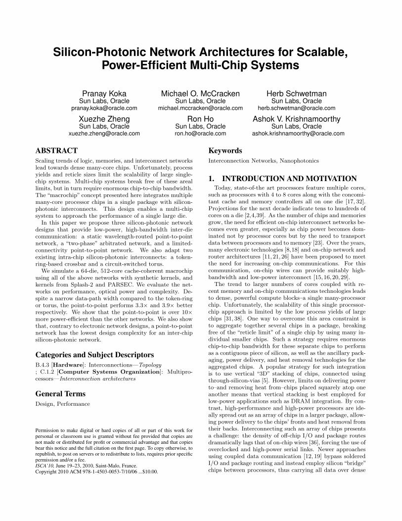
Figure 1: Physical Layout of a 4×4 Macrochip. TwoFace-Down CPU Die Are Shown At An Angle.
greater die-to-die bandwidth but uses optical switches. Wealso evaluate the performance, power, and complexity ofthese networks in a macrochip-like architecture.
Because no prior work has focused on a macrochip-likeshared memory multiprocessor, we adapt two promising sili-con photonic intra-chip network architectures to the macro-chip layout and technology as a point of comparison. Weperform a thorough simulation-based performance evalua-tion of all five network architectures on two of the SPLASH-2 shared-memory benchmarks [42], three of the PARSECbenchmarks [6], and four synthetic benchmarks.
The contributions of this paper include:
• An architectural introduction to the macrochip, a tech-nology platform for a computing system embodying asilicon-photonic intra-die interconnection network withhigh peak aggregate bandwidth, low latency and lowpower.
• A classification of optical on-chip networks.
• Three interconnection network topologies designed forthe macrochip, two previously unpublished. One net-work is optimized for all-to-all communications pat-terns and the other two offer improved link bandwidths.
• A thorough performance, power and complexity eval-uation of all network architectures.
The rest of the paper is organized as follows. In section 2,we describe the enabling silicon-photonic technology with re-gards to the various optical components used including theirpower, bandwidth and latencies. In section 3, we present abrief description of the macrochip architecture and give someof its advantages. In section 4, we describe the architectureand design of the three proposed network architectures alongwith the adapted reference architectures. In sections 5 and6, we describe our evaluation methodology and analyze ourresults. Finally we survey the background work in relatedareas in section 7 and conclude in section 8.
2. SILICON-PHOTONIC TECHNOLOGYIn this section, we give a brief overview of the silicon-
photonic components used in a macrochip. A macrochipconsists of a large silicon routing substrate containing op-tical waveguides. This routing layer has chip-sized openingsetched into its surface, and in each opening (called a site) is aprocessor chip with several cores and caches, and a memory
waveguides
Inter-layer coupler w/ integrated
mirrors
Laser, !0
data
modulator
detector TIA
data
"#
RX site TX site
SOI substrate
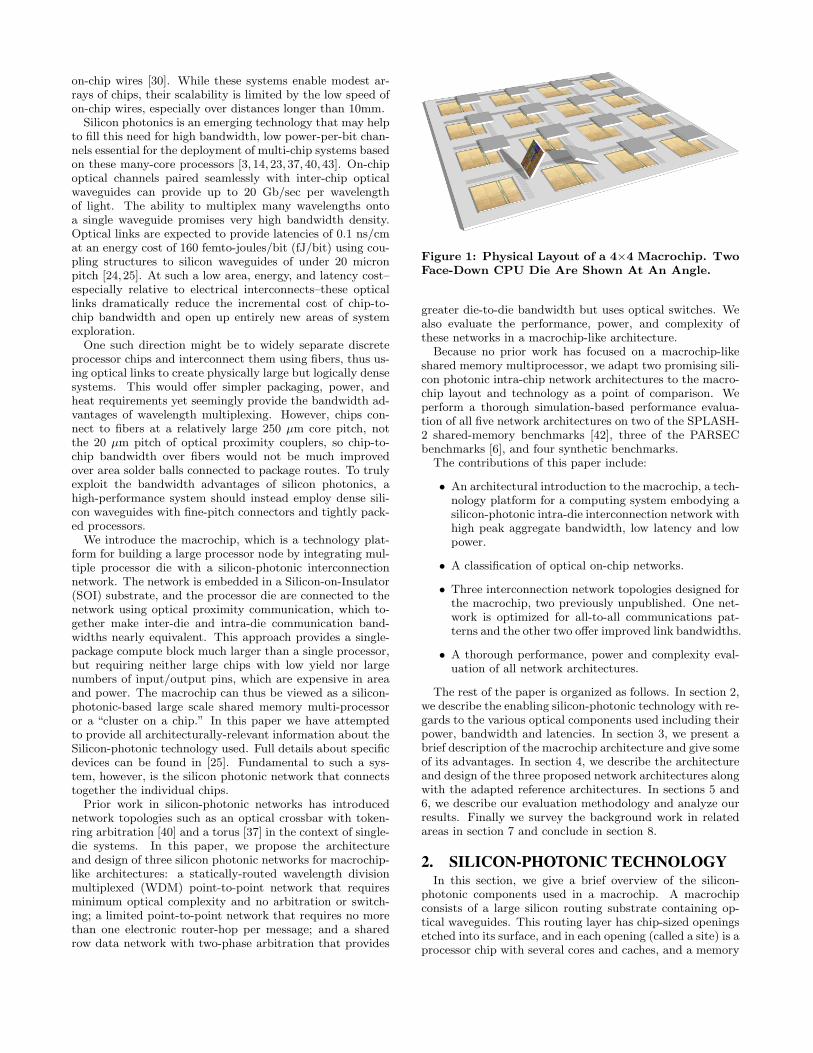
Figure 2: A Single Photonic Link. Not Shown Are Mux/Demux Devices for WDM.
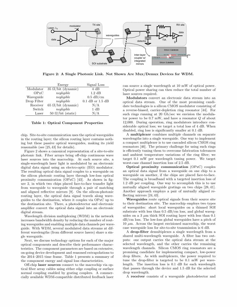
Energy Signal LossModulator 35 fJ/bit (dynamic) 4 dB
OPxC negligible 1.2 dBWaveguide negligible 0.5 dB/cm
Drop Filter negligible 0.1 dB or 1.5 dBReceiver 65 fJ/bit (dynamic) N/A
Switch negligible 1 dBLaser 50 fJ/bit (static) N/A
Table 1: Optical Component Properties
chip. Site-to-site communication uses the optical waveguidesin the routing layer; the silicon routing layer contains noth-ing but these passive optical waveguides, making its yieldreasonable (see [25,43] for details).
Figure 2 shows a canonical representation of a site-to-sitephotonic link. Fiber arrays bring off-chip continuous wavelaser sources into the macrochip. At each source site, asingle-wavelength laser light is modulated by an electronicdigital data signal using an electro-optic (EO) modulator.The resulting optical data signal couples to a waveguide onthe silicon photonic routing layer through low-loss opticalproximity communication (OPxC) [43]. As shown in fig-ure 2, in which two chips placed face-to-face transfer lightfrom waveguide to waveguide through a pair of matchingand aligned reflective mirrors [9]. On the silicon-photonicrouting layer, the optical data signal travels along wave-guides to the destination, where it couples via OPxC up tothe destination site. There, a photodetector and electronicamplifier convert the optical data signal into an electronicdigital stream.
Wavelength division multiplexing (WDM) in the networkincreases bandwidth density by reducing the number of rout-ing waveguides and enabling multiple data channels per wave-guide. With WDM, several modulated data streams at dif-ferent wavelengths (from different source lasers) share a sin-gle waveguide.
Next, we discuss technology options for each of the majoroptical components and describe their performance charac-teristics. The component parameters are based on extensive,on-going device development and reasoned extrapolations tothe 2014–2015 time frame. Table 1 presents a summary ofthe component energy and signal loss characteristics.
Off-chip laser sources connect to the macrochip via op-tical fiber array cables using either edge coupling or surfacenormal coupling enabled by grating couplers. A commer-cially available WDM-compatible distributed feedback laser
can source a single wavelength at 10 mW of optical power.Optical power sharing can then reduce the total number oflaser sources required.
Modulators convert an electronic data stream into anoptical data stream. One of the most promising candi-date technologies is a silicon CMOS modulator consisting ofa reverse-biased, carrier-depletion ring resonator [44]. Forsuch rings running at 20 Gb/sec we envision the modula-tor power to be 0.7 mW, and have a resonator Q of about12,000. During operation, ring modulators introduce con-siderable optical loss; we target a total loss of 4 dB. Whendisabled, ring loss is significantly smaller at 0.1 dB.
A multiplexer combines multiple channels on separatewavelengths into a single waveguide. One way to implementa compact multiplexer is to use cascaded silicon CMOS ringresonators [46]. The primary challenge for using such ringsis efficiently tuning them to overcome fabrication tolerancesand ambient temperature variations of the ring filter; wetarget 0.1 mW per wavelength tuning power. We targetworst-case channel insertion loss of 2.5 dB.
Optical proximity communication (OPxC) couplesan optical data signal from a waveguide on one chip to awaveguide on another, if the chips are placed face-to-face.The coupling is broadband with a targeted insertion loss of1.2 dB per coupling. One way to accomplish this is to usemutually aligned waveguide gratings on two chips [28, 41].Another approach employs a pair of mutually aligned re-flecting mirrors [24,43].
Waveguides route optical signals from their source siteto their destination site. The macrochip employs two typesof waveguides: short local waveguides on a thinned SOIsubstrate with less than 0.5 dB/cm loss, and global waveg-uides on a 3 µm thick SOI routing layer with less than 0.1dB/cm loss. The low-loss global waveguides have a pitch of10 µm. Across the largest envisioned macrochip, the worstcase waveguide loss for site-to-site transmission is 6 dB.
A drop-filter demultiplexes a single wavelength from ashared multi-wavelength waveguide. A filter has two out-puts: one output carries the optical data stream at theselected wavelength, and the other carries the remainingwavelength channels. Silicon CMOS ring resonators are apromising candidate for implementing compact, low-powerdrop filters. As with multiplexers, the power required totune the drop-filter is targeted to be 0.1 mW per wave-length. The insertion loss is 0.1 dB for each wavelengththat passes through the device and 1.5 dB for the selecteddrop wavelength.
A receiver consists of a waveguide photodetector and
2 Rx1 Rx3 Rx
0 RxInter-layer couplerWDM Drop Filter
Data Waveguide
Data Message
WDM Multiplexer
Modulator
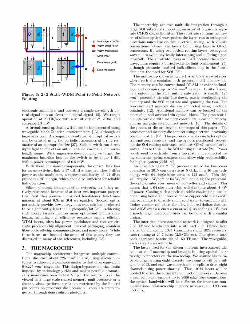
Figure 3: 2×2 Static-WDM Point to Point NetworkRouting
electronic amplifiers, and converts a single-wavelength op-tical signal into an electronic digital signal [45]. We targetoperation at 20 Gb/sec with a sensitivity of -21 dBm, andconsume 1.3 mW.
A broadband optical switch can be implemented usingwaveguide Mach-Zehnder interferometers [13], although atlarge area cost. A compact quasi-broadband optical switchcan be created using the periodic resonances of a ring res-onator of an appropriate size [27]. Such a switch can directinput light to one of two output channels over a 30 nm wave-length range. With aggressive development, we target themaximum insertion loss for the switch to be under 1 dB,with a power consumption of 0.5 mW.
With these envisioned components, the optical link lossfor an un-switched link is 17 dB. If a laser launches 0 dBmpower at the modulator, a receiver sensitivity of -21 dBmprovides 4 dB margin, which should be sufficient for reliablelink operation.
Silicon photonic interconnection networks are being ac-tively researched because of at least two important proper-ties. First, they promise high-speed, low-latency data trans-mission, at about 0.3c in SOI waveguides. Second, opticspotentially provides low energy data transmission, projectedto be significantly less than 1 picojoule/bit [25]. Achievingsuch energy targets involves many optics and circuits chal-lenges, including high efficiency resonator tuning, efficientWDM lasers, ultra-low power modulator and receiver cir-cuits, precision chip alignment, low cost packaging, seamlessfiber-optic off-chip communications, and many more. Whilethese issues are beyond the scope of this paper, they arediscussed in many of the references, including [25].
3. THE MACROCHIPThe macrochip architecture integrates multiple conven-
tional die, each about 225 mm2 in size, using silicon pho-tonics to achieve performance similar to that of an equivalent64x225 mm2 single die. This design bypasses die size limitsimposed by technology yields and makes possible dramati-cally more cores on a virtual “chip.” The macrochip can beviewed as a large scale shared-memory multiprocessor or acluster, whose performance is not restricted by the limitedpin counts on processor die because all cores are intercon-nected through dense silicon photonics.
The macrochip achieves multi-die integration through alarge SOI substrate supporting an array of physically sepa-rate CMOS die, called sites. The substrate contains two lay-ers of silicon optical waveguides; the layers run in orthogonaldirections much like on-chip electrical wiring, with via-likeconnections between the layers built using low-loss OPxCconnectors. By using two optical routing layers, orthogonalwaveguides avoid physically intersecting and suffering signalcrosstalk. The substrate layers are SOI because the siliconwaveguides require a buried oxide for light confinement [25],although photonics-enabled bulk silicon may in the futureeliminate the need for SOI [33].
The macrochip shown in figure 1 is an 8×8 array of sites,where each site contains both processor and memory die.The memory can be conventional DRAM or other technol-ogy, and occupies up to 225 mm2 in area. It sits face-upin a cutout in the SOI routing substrate. A smaller 125mm2 processor die sits face-down, partly overlapping thememory and the SOI substrate and spanning the two. Theprocessor and memory die are connected using electricalproximity [12]. Additional memory can be located off themacrochip and accessed via optical fibers. The processor isa multi-core die with memory controllers, a cache hierarchy,and an intra-die interconnect network [10]. The details ofthe processor die are beyond the scope of this paper. Theprocessor and memory die connect using electrical proximitycommunication [12]. The processor die also includes opticaltransmitters, receivers, and waveguides positioned to over-lap the SOI routing substrate, and uses OPxC to connect itswaveguides to those in the SOI routing substrate [24]. Poweris delivered to each site from a top plate and connected us-ing solderless spring contacts that allow chip replaceabilityfor higher system yield [30].
An Oracle Niagara 2 [32] processor scaled for low-poweroperation in 2015 can operate at 5 GHz, in a 16 nm tech-nology with 64 single-issue cores in 125 mm2. This chipwill require 1 W/core or 64 W/site, including the processor,the optical interfaces, memory controller and caches. Thismeans that a 64-site macrochip will dissipate about 4 kWof power. Cooling such a package, while challenging, can bedone using liquid and direct-bonded copper cold plates withmicrochannels to directly shunt cold water to each chip site.Today, vendors sell plates for a few hundred dollars that cancool 3 kW over a 5 cm x 5 cm area [1], so cooling 4 kW overa much larger macrochip area can be done with a similardesign.
The inter-site interconnection network is designed to offer2.56 TB/sec bandwidth into a site and 2.56 TB/sec froma site, by employing 1024 transmitters and 1024 receivers,each running at 20 Gb/sec (2.5 GB/sec). This gives a totalpeak aggregate bandwidth of 160 TB/sec. The waveguideseach carry 16 wavelengths.
The lasers used for the silicon photonic interconnect willbe located off-macrochip and brought in using optical fibersto edge connectors on the macrochip. We assume lasers ca-pable of generating eight discrete wavelengths will be avail-able in 2015, and each wavelength can be split to drive eightchannels using power sharing. Thus, 1024 lasers will beneeded to drive the entire interconnection network. Becausea macrochip can support up to 2000 edge fiber connections,the optical bandwidth will be sufficient for inter-site com-munications, off-macrochip memory accesses, and I/O con-nections.
The macrochip architecture as described enables buildinga large-scale shared-memory multiprocessor in a single log-ical chip made up of 64 die. The remainder of this paperis devoted to describing five different network designs forconnecting these die and, for each design, evaluating perfor-mance, power and complexity.
4. NETWORK ARCHITECTURESSection 3 described a target system for the 2015 time
frame. However, simulating such a large system is currentlyintractable. Therefore, in the following sections we describeand analyze a scaled-down system where both the computepower and network bandwidth are reduced by a factor ofeight. Therefore, each site has 128 transmitters and 128 re-ceivers, the total peak network bandwidth is 20 TB/sec, andthere are 8 wavelengths per waveguide and 8 cores per site.These are detailed in tables 4 and 6.
4.1 Classification of Optical Network Archi-tectures
Implementing electronic dynamic packet switching is rela-tively straightforward. Therefore, designers of conventionalon-chip networks can choose from a wide range of multi-hopnetwork topologies [10]. However, optical dynamic packetswitching is much more difficult. A switched optical net-work is either circuit switched, using dynamically set opticalswitches; or requires multiple optical-electrical conversionsand routing in the electronic domain. The goal of this paperis to propose and evaluate optical network architectures ofvarious types for the macrochip. Based on the switching orrouting architecture used by the network, we classify opticalnetwork topologies into the four broad categories below.
Optical Networks Without Switching or Routing. The onlynetwork that falls under this category is a fully connectedoptical point-to-point network. A fully connected electronicpoint-to-point network is difficult to implement due to thequadratic growth in the number of wires and connections.In the optical domain, however, we exploit WDM in siliconwaveguides to reduce waveguide area and routing complex-ity. We show in section 6.4 that a point-to-point networkis less complex than other, switch-based architectures. Apoint-to-point networks has almost no overhead for datatransmission, but is limited to low-bandwidth and narrowdatapath site-to-site optical channels.
Circuit Switched Networks. These architectures use a net-work of waveguides and optical switches with multiple hostaccess points to interconnect compute nodes. Each com-pute node sets up a series of optical switches, using an in-dependent optical/electrical path-setup network, to connectthe node to the destination. No explicit arbitration amongsenders is required for data transmission. Depending on thetopology and complexity, these networks are either blockingor non-blocking. A non-blocking network implies that a cir-cuit established between any pair of nodes ’A’ and ’B’ willnot block a circuit between any other pair of nodes ’C’ and’D’. We adapt the architecture of the optical circuit-switchtorus proposed in [35] to the macrochip technology.
Arbitration-Based Switched Optical Networks. Arbitrated net-works are fundamentally circuit switched networks but differ
in the way the optical circuit is established. All sources con-tending for a shared data channel arbitrate for data slotsprior to data transmission. The arbitration mechanism alsosets up the appropriate switches for data transmission. Thesenetworks usually require a separate arbitration network forcontrol. One proposed optical crossbar architecture uses op-tical token ring arbitration to access the network [40]. Weadapt this network topology to the macrochip architecture.Based on our power analysis we find the crossbar archi-tecture has high power consumption when adapted to themacrochip. We propose a two-phase arbitration-based net-work that has lower power requirements at the expense oflower site-to-site bandwidth than the network in [40].
Optical Networks with Electronic Routing. These networksuse multiple hops between the source and destination nodes;however at each hop, the optical packets are converted tothe electronic domain, packet switched to the appropriateoutput port, and then converted back to the optical domain.We modify the point-to-point network (above) to limit thenumber of direct connections and use a maximum of oneelectronic switching hop in order to provide full connectivityin the network. This facilitates higher bandwidth site-to-siteoptical channels compared to the point-to-point network.
The five networks chosen for the macrochip have remark-ably different properties. The point-to-point network hasthe least overhead but is limited by low-bandwidth narrow-datapath site-to-site channels whereas the switched networkshave higher bandwidth wider-data-path data channels butwith higher overhead in the form of arbitration, path setupor electronic routing.
4.2 Statically-Routed Point-to-Point NetworkIn the static WDM-routed point-to-point network, each
site has a dedicated optical data path to every other site.Figure 3 shows a 2 × 2 point-to-point network. The figureshows a packet transfer from site 0 to sites 1 and 3. Site0 uses the same horizontal and vertical waveguide for bothtransfers, but uses a different wavelength for each destina-tion, blue for site 3 and red for site 1.
The network layout consists of horizontal waveguides be-tween the rows of the macrochip and vertical waveguidesbetween the columns of the macrochip. The horizontal andvertical waveguides are laid on the bottom and top layers,respectively, of the SOI routing substrate, and horizontalwaveguides connect to vertical waveguides using inter-layercouplers. Each vertical waveguide drops one wavelength ateach site in the column. A transmitting site can communi-cate with any receiving site S by choosing the waveguidesleading to the column of site S and the wavelength that isthen dropped at site S.
In the 8× 8 macrochip configuration, each site sources 16horizontal waveguides, each carrying 8 wavelengths of light,for a total of 128 wavelengths. At a bit-rate of 20 Gb/sec(2.5 GB/sec) per wavelength, and with 64 sites, the networkhas a total peak bandwidth of 20 TB/sec. Each point-to-point data channel uses two wavelengths for 5 GB/sec. Thenetwork uses 8192 total horizontal and twice as many verti-cal waveguides, because each vertical channel consists of twowaveguides for communicating both up and down. A moredetailed component count is presented in table 6.
The statically routed point-to-point network has no switch-ing or arbitration overheads. However, the narrow 2-bit site-
0 1
2 3T TT T
T T T T
x
x x
x
x xx
x
x
x x
x
x
x x
x
x x
x
x x
x
x
xA B
C
1x2 switch
Inter-layer coupler
WDM Drop Filter
Splitter
T 1xN Tree Switch
Data Waveguide
Arbitration Waveguide
Arbitration Message
Data Message
Site 0 sends to S3. First, S0 sends an arb. request in blue along
its row. An arb. slot is assigned to the request. Then S1 sends
the switch request in red along the column. S3 sets the input
switch. Finally, S0 sends using the data waveguide going to S3.
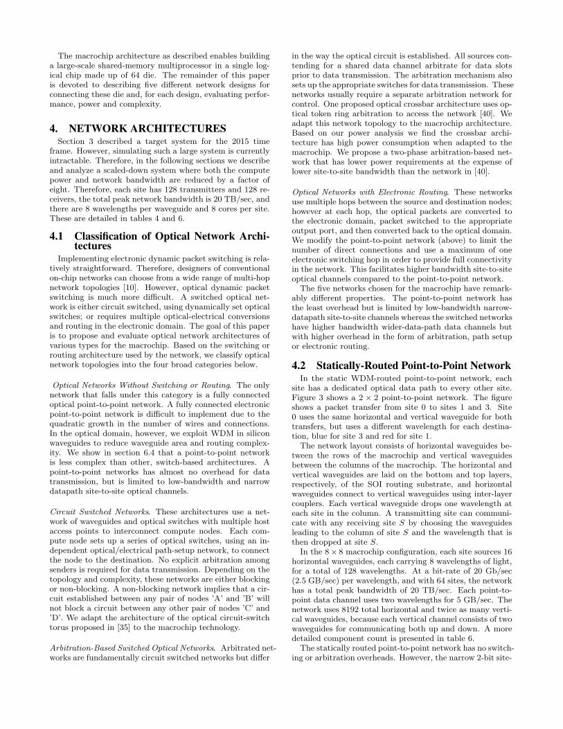
Figure 4: Two-Phase Arbitrated Network
to-site data-path is a potential performance limiter. Thisobservation motivates the investigation of other types of net-works with higher point-to-point bandwidth.
4.3 Two-Phase Arbitration-Based Switched Op-tical Network
Data Network Topology. This architecture uses shared datachannels between sites to increase the bandwidth per site-to-site logical connection. Figure 4 shows a small 2× 2 versionof the macrochip with this network. All sites in a row ofthe macrochip share an optical data channel to one othersite. Thus, an 8 × 8 macrochip has 512 shared channels.Sites that share a channel are said to belong to the samearbitration domain. Each site connects to 64 shared hori-zontal channels, each comprised of two waveguides with 8wavelengths per waveguide. Each of the waveguides in arow is coupled to a vertical waveguide using an inter-layercoupler, and this vertical waveguide is connected to one des-tination site. Each shared channel is 40 GB/sec and 16 bitswide. Due to the physical restriction that only one trans-mitter at a time can feed directly into a waveguide, a sharedwaveguide is implemented using broadband switches at thefeeding points. Each switch hop along the path of an opticalsignal causes 1 dB loss. To minimize the optical loss throughthe switches, each waveguide is implemented as two paral-lel waveguide segments. We refer to the pair of segmentsthat form a logical waveguide as simply waveguides in thissection.
In order to minimize the number of transmitters in thenetwork, each site is limited to transmitting to only one sitein any column and hence can sustain, at most, 8 simultane-ous 40 GB/sec transmissions to different columns. Each siteuses a tree of broadband switches per column, shown as ”T”in figure 4, to choose a destination in that column. This re-sults in a maximum of 7 switch hops between any source anddestination and hence only a 7 dB loss. The use of switchtrees to minimize the number of switches on a path can re-sult in contention when a site has multiple packets to sendto a single column. An alternate version of this network uses
twice the amount of laser power and double the number ofswitch trees, to reduce the potential for contention. This al-ternative, called ”2-phase Arb ALT” in the remainder of thepaper, is evaluated along with the base design in section 6.
Arbitration Network Topology. Figure 4 illustrates the topol-ogy and operation of the arbitration network. Due to themesochronous properties of the macrochip [25], we can em-ploy a completely distributed arbitration mechanism to re-duce the arbitration overheads. Each node in an arbitrationdomain makes the same decision for every arbitration re-quest as made by all of the sites in that domain, at thesame time.
Data transmission from any site ’A’ to any site ’B’ re-quires contention resolution among the sites in the arbitra-tion domain and a control operation to set the appropriateswitches for data transmission. The arbitration network con-sists of a request waveguide for each row for contention res-olution, and a notification waveguide for each column to setthe appropriate destination switches. Each site can trans-mit on the request and the notification waveguides usingpre-assigned wavelengths. In addition, each site is a columnmanager of its column in its arbitration domain. The arbi-tration wavelengths are assigned in cyclic fashion as shownin figure 4, to enable WDM and reduce the number of ar-bitration waveguides. The request waveguides are snoopedby all sites in the corresponding row, and the notificationwaveguides are snooped by the all sites in the correspond-ing column. Snooping requires higher input power propor-tional to the number of sites snooping the waveguide. In thiscase the arbitration waveguides need to be sourced with 7×more laser power. Since the arbitration network uses a smallnumber of lasers (in comparison to the data network), theincrease in power is negligible. The increase in area due toarbitration is also small, because it adds only 16 horizontaland 8 vertical waveguides to the data network.
Arbitration Mechanism. Sites arbitrate for access to a des-tination in arbitration slots. Each arbitration slot is about0.4 ns, enough to transmit an arbitration request. Multiplearbitration requests are pipelined to improve bandwidth uti-lization on the optical data channels. The data channels areare also time-slotted. The size of each slot is variable butan integral multiple of a basic slot size. Data transmissionfor every packet requires the following steps:
Phase 1:1) All requests during an arbitration interval are posted
to the request network.2) Each site in the arbitration domain sees the request
after the propagation time.3) Each site maintains a round-robin counter for every
destination node. The counter specifies the order of assign-ment of successive slots to the requesters. All sites in thearbitration domain assign the same slot Tr to a requester.
Phase 2:1) At arbitration slot Ta, Ta < Tr, the column manager
for the destination column sends a switch request on thenotification waveguide in the pre-assigned wavelength.
2) Prior to slot Tr, all the row sites in the arbitrationdomain set their respective broadband switches, the desti-nation site sets its input-select switch, and the source sitetransmits the data over the optical circuit to the destination.
The switch request notification is timed to accommodate
the switch delay. When an optical switch is set, it remainsin that position until another switch request notificationchanges it.
This network provides a wider 16-bit 40 GB/sec data pathbut incurs arbitration and switch-delay overheads. A de-tailed component count for the data and arbitration net-works is given in table 6.
4.4 Token-Ring-Based Optical CrossbarThe Corona architecture is an optical crossbar with token-
ring arbitration, using a ring topology with no waveguidecrossings [40]. Each site or cluster in the Corona architec-ture has a dedicated waveguide bundle shared by all sitestransmitting data to that site. Access to the shared bundleis arbitrated using a token ring. One token for each destina-tion is propagated on a token bus by that site. A site thatneeds to transmit data to the destination diverts the tokenby tuning its receiver on the token channel to the correctwavelength. On completing data transmission, the site re-leases the token by re-injecting a light pulse into the tokenbus. We adapted the Corona network to the macrochip byusing the bottom substrate to route both the token and datawaveguides and the modulators.
The Corona network architecture uses 64-way WDM andhence each wavelength of light passes by 4,096 modulatorrings. Each modulator when tuned off-resonance causes a0.1 dB loss to the signal causing a 409.6 dB loss along thepath. Even a WDM factor of 8 as used by the macrochip,causes a 51.2 dB loss. In order to limit the power loss dueto the rings to 12.8 dB, we reduced the WDM factor to 2and increased the number of waveguides by a factor of 4.
The macrochip dimensions are 10× the dimensions of thechip proposed for Corona. We scaled the 8 cycle round-trip token latency specified in [40] based on dimension. Inour adaptation, it takes 80 cycles for a token to complete around-trip.
4.5 Circuit Switched NetworkA circuit switched network requires a path setup proce-
dure to set the appropriate optical switches along the pathfrom the source to the destination. The circuit-switched-style network in [35] uses an electronic torus overlaying anoptical torus. The optical torus uses a 4 × 4 optical switchat each switching point. This optical torus network enablesnon-blocking operation. The electronic network is a low-bandwidth packet-switched network and is used to set upan optical path from the source to the destination. Eachswitching point in the electronic network is attached to the4 × 4 optical switch that it controls. To establish an op-tical circuit, a source node initiates a path-setup packet onthe electronic network from its gateway; this setup packet isrouted through multiple switch points to the destination. Ateach switch point the router sets the corresponding opticalswitch and routes the packet towards the destination site.Similarly, a post-communication path-breakdown procedureis followed to tear down the optical circuit.
We adapted the network topology and architecture in [35]for the macrochip. Adding an inter-site electronic networkfor path setup on the macrochip would require an activesubstrate with long running wires/lines, complicating thedesign of the macrochip. Therefore, in our adaptation, weused a low bandwidth optical network for path setup insteadof an electronic network.
0 1 2
6 7
53 4
8
Mux with LayerCoupler
Intra-Layer Coupler8 ModulatorsLaser Source
Router
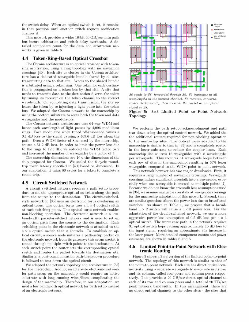
S0 sends to S8, forwarded through S6. S0 transmits in all
wavelengths in the marked channel. S6 receives, converts,
routes electronically, then re-sends the packet as an optical
signal to S8.
Figure 5: 3×3 Limited Point to Point NetworkTopology
We perform the path setup, acknowledgment and pathtear-down using the optical control network. We added thethe additional routers required for non-blocking operationto the macrochip sites. The optical torus adapted to themacrochip is similar to that in [35] and is completely routedin the lower substrate to reduce the coupler loses. Eachmacrochip site sources 16 waveguides with 8 wavelengthsper waveguide. This requires 64 waveguide loops betweeneach row of sites in the macrochip, resulting in 50% fewerwaveguides compared to the WDM point-to-point network.
This network however has two major drawbacks. First, itrequires a large number of waveguide crossings. Waveguidecrossings induce significant crosstalk into a waveguide, espe-cially when one waveguide is crossed at multiple points [7].Because we do not know the crosstalk loss assumptions usedin [35], we assume negligible crosstalk at waveguide crossingsfor the macrochip adaptation of this network. Second, thereare similar questions about the power loss due to broadbandswitches. As shown in Table 1, we project that a broad-band 1 × 2 switch will cause a 1 dB power loss. For theadaptation of the circuit-switched network, we use a moreaggressive power loss assumption of 0.5 dB loss per 4 × 4optical switch. The worst case path in the network requires31 optical switch hops causing approximately 15 dB loss tothe input signal, requiring an approximate 30x increase inthe laser power. More detailed component counts and powerestimates are shown in tables 6 and 5.
4.6 Limited Point-to-Point Network with Elec-tronic Routing
Figure 5 shows a 3×3 version of the limited point-to-pointnetwork. The topology of this network is similar to that ofthe point-to-point network. Each site has direct optical con-nectivity using a separate waveguide to every site in its rowand its column, called row-peers and column-peers respec-tively. This provides a 20 GB/sec direct optical channel toeach of its row and column peers and a total of 20 TB/secpeak network bandwidth. In this arrangement, there areno direct optical channels to the other sites - the sites that
are not in the row or column of the source site. Electronicrouting is used to extend the connectivity of a site to theremaining sites. This routing is implemented by adding two7×7 electronic routers on each site: one for forwarding pack-ets from row peers to column peers and one for forwardingfrom column peers to row peers. Communication betweennon-peer sites requires that a data packet be first forwardedto a site that is a peer to both the source and the destina-tion. At the forwarding site, the data packet is convertedto the electronic domain, forwarded to the appropriate out-put port, and then converted back to the optical domainto reach the destination. By the use of this configuration,each transmission requires a maximum of one intermediateO-E/E-O conversion. Table 6 gives the component count forthis network architecture. The routers used in the sites areassumed to have a latency of one cycle.
5. SIMULATION METHODOLOGYWe performed a detailed evaluation of the five network
architectures for the macrochip using two kinds of work-loads: application kernels and synthetic benchmarks. Weused five shared memory application benchmarks, two fromthe SPLASH-2 suite and three from the PARSEC suite. Thebenchmarks and the data sets used are listed in Table 2. TheSPLASH-2 benchmarks were compiled with the Sun Studio12 compiler suite with -fast optimization and the PARSECbenchmarks were compiled using g++ version 3.4.3 with -O3
optimization for the UltraSparc T2+ processor.The four synthetic benchmarks were chosen to represent a
range of traffic patterns. In the butterfly and transpose pat-tern, each site only sends to one unique destination, whereasin the nearest-neighbor pattern, each site communicates withfour neighbors. Table 3 lists and describes the syntheticbenchmarks. These benchmarks were driven by two typesof coherence mixes: Less Sharing (LS) and More Sharing(MS). In the LS mix, 90% of coherence requests have nosharers for the cache block, while in the MS mix, 40% of re-quests have three sharers. All of the synthetic benchmarksare driven at a rate equivalent to an L2 cache miss rate of4% per instruction.
Table 4 shows the simulated macrochip configuration. Wereduced the number of cores per site from 64, in the config-uration proposed in section 3, to 8 to make the simulationmore tractable. Accordingly we reduced the total networkbandwidth by 8 times, to a peak of 20 TB/sec for all thenetworks. We also used a 256 KB cache, shared by all coreson the site, to suit the data set sizes of the applications.The optical-fiber-connected main memory is not modeled indetail. We leave the study of effect of main memory tech-nologies on performance to future work.
Our simulation infrastructure consists of two parts. Themacrochip CPU simulator is an instruction-trace driven mul-tiprocessor core/cache simulator that models an MOESI co-herence protocol. The CPU simulator generates L2 misstraffic along with detailed coherence information for all 512cores. The network simulator models all five network archi-tectures and is driven using the coherence traffic generatedby the CPU simulator. The network model simulates all nec-essary network messages required by the coherence protocolto satisfy a coherence request. We model finite MSHRs, net-work I/O buffers and virtual channels for cache coherenceoperations. To keep simulation time manageable, we do notmodel the intricate details of the cache coherency protocol.
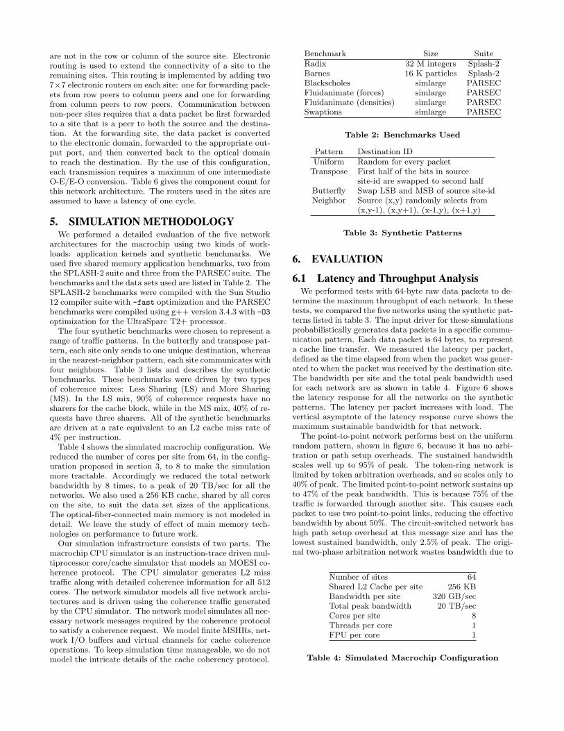
Benchmark Size SuiteRadix 32 M integers Splash-2Barnes 16 K particles Splash-2Blackscholes simlarge PARSECFluidanimate (forces) simlarge PARSECFluidanimate (densities) simlarge PARSECSwaptions simlarge PARSEC
Table 2: Benchmarks Used
Pattern Destination IDUniform Random for every packet
Transpose First half of the bits in sourcesite-id are swapped to second half
Butterfly Swap LSB and MSB of source site-idNeighbor Source (x,y) randomly selects from
(x,y-1), (x,y+1), (x-1,y), (x+1,y)
Table 3: Synthetic Patterns
6. EVALUATION
6.1 Latency and Throughput AnalysisWe performed tests with 64-byte raw data packets to de-
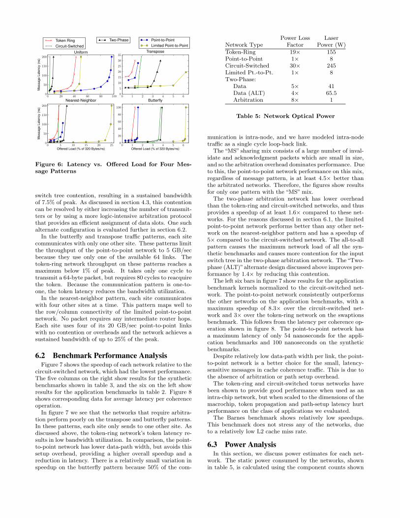
termine the maximum throughput of each network. In thesetests, we compared the five networks using the synthetic pat-terns listed in table 3. The input driver for these simulationsprobabilistically generates data packets in a specific commu-nication pattern. Each data packet is 64 bytes, to representa cache line transfer. We measured the latency per packet,defined as the time elapsed from when the packet was gener-ated to when the packet was received by the destination site.The bandwidth per site and the total peak bandwidth usedfor each network are as shown in table 4. Figure 6 showsthe latency response for all the networks on the syntheticpatterns. The latency per packet increases with load. Thevertical asymptote of the latency response curve shows themaximum sustainable bandwidth for that network.
The point-to-point network performs best on the uniformrandom pattern, shown in figure 6, because it has no arbi-tration or path setup overheads. The sustained bandwidthscales well up to 95% of peak. The token-ring network islimited by token arbitration overheads, and so scales only to40% of peak. The limited point-to-point network sustains upto 47% of the peak bandwidth. This is because 75% of thetraffic is forwarded through another site. This causes eachpacket to use two point-to-point links, reducing the effectivebandwidth by about 50%. The circuit-switched network hashigh path setup overhead at this message size and has thelowest sustained bandwidth, only 2.5% of peak. The origi-nal two-phase arbitration network wastes bandwidth due to
Number of sites 64Shared L2 Cache per site 256 KBBandwidth per site 320 GB/secTotal peak bandwidth 20 TB/secCores per site 8Threads per core 1FPU per core 1
Table 4: Simulated Macrochip Configuration
0 20 40 60 80 1000
50
100
150
200
Mes
sage
Late
ncy
(ns)
Uniform
0 1 2 3 4 5 60
5
10
15
20
25
30
35Transpose
0 5 10 15 20 25Offered Load (% of 320 Bytes/ns)
0
50
100
150
200
Mes
sage
Late
ncy
(ns)
Nearest-Neighbor
0 1 2 3 4 5 6Offered Load (% of 320 Bytes/ns)
0
20
40
60
80
100
Butterfly
Token RingCircuit-Switched
Point-to-PointLimited Point-to-Point
Two-Phase
Figure 6: Latency vs. Offered Load for Four Mes-sage Patterns
switch tree contention, resulting in a sustained bandwidthof 7.5% of peak. As discussed in section 4.3, this contentioncan be resolved by either increasing the number of transmit-ters or by using a more logic-intensive arbitration protocolthat provides an efficient assignment of data slots. One suchalternate configuration is evaluated further in section 6.2.
In the butterfly and transpose traffic patterns, each sitecommunicates with only one other site. These patterns limitthe throughput of the point-to-point network to 5 GB/secbecause they use only one of the available 64 links. Thetoken-ring network throughput on these patterns reaches amaximum below 1% of peak. It takes only one cycle totransmit a 64-byte packet, but requires 80 cycles to reacquirethe token. Because the communication pattern is one-to-one, the token latency reduces the bandwidth utilization.
In the nearest-neighbor pattern, each site communicateswith four other sites at a time. This pattern maps well tothe row/column connectivity of the limited point-to-pointnetwork. No packet requires any intermediate router hops.Each site uses four of its 20 GB/sec point-to-point linkswith no contention or overheads and the network achieves asustained bandwidth of up to 25% of the peak.
6.2 Benchmark Performance AnalysisFigure 7 shows the speedup of each network relative to the
circuit-switched network, which had the lowest performance.The five columns on the right show results for the syntheticbenchmarks shown in table 3, and the six on the left showresults for the application benchmarks in table 2. Figure 8shows corresponding data for average latency per coherenceoperation.
In figure 7 we see that the networks that require arbitra-tion perform poorly on the transpose and butterfly patterns.In these patterns, each site only sends to one other site. Asdiscussed above, the token-ring network’s token latency re-sults in low bandwidth utilization. In comparison, the point-to-point network has lower data-path width, but avoids thissetup overhead, providing a higher overall speedup and areduction in latency. There is a relatively small variation inspeedup on the butterfly pattern because 50% of the com-
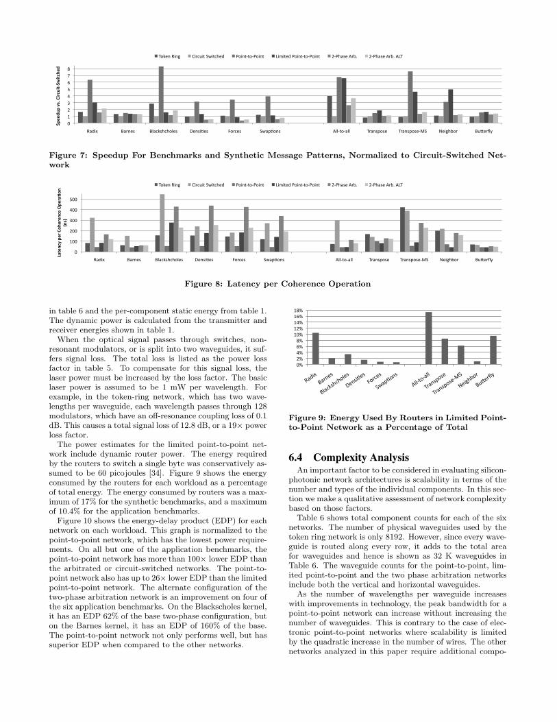
Power Loss LaserNetwork Type Factor Power (W)Token-Ring 19× 155Point-to-Point 1× 8Circuit-Switched 30× 245Limited Pt.-to-Pt. 1× 8Two-Phase:
Data 5× 41Data (ALT) 4× 65.5Arbitration 8× 1
Table 5: Network Optical Power
munication is intra-node, and we have modeled intra-nodetraffic as a single cycle loop-back link.
The “MS” sharing mix consists of a large number of inval-idate and acknowledgment packets which are small in size,and so the arbitration overhead dominates performance. Dueto this, the point-to-point network performance on this mix,regardless of message pattern, is at least 4.5× better thanthe arbitrated networks. Therefore, the figures show resultsfor only one pattern with the “MS” mix.
The two-phase arbitration network has lower overheadthan the token-ring and circuit-switched networks, and thusprovides a speedup of at least 1.6× compared to these net-works. For the reasons discussed in section 6.1, the limitedpoint-to-point network performs better than any other net-work on the nearest-neighbor pattern and has a speedup of5× compared to the circuit-switched network. The all-to-allpattern causes the maximum network load of all the syn-thetic benchmarks and causes more contention for the inputswitch tree in the two-phase arbitration network. The“Two-phase (ALT)”alternate design discussed above improves per-formance by 1.4× by reducing this contention.
The left six bars in figure 7 show results for the applicationbenchmark kernels normalized to the circuit-switched net-work. The point-to-point network consistently outperformsthe other networks on the application benchmarks, with amaximum speedup of 8.3× over the circuit-switched net-work and 3× over the token-ring network on the swaptionsbenchmark. This follows from the latency per coherence op-eration shown in figure 8. The point-to-point network hasa maximum latency of only 54 nanoseconds for the appli-cation benchmarks and 100 nanoseconds on the syntheticbenchmarks.
Despite relatively low data-path width per link, the point-to-point network is a better choice for the small, latency-sensitive messages in cache coherence traffic. This is due tothe absence of arbitration or path setup overhead.
The token-ring and circuit-switched torus networks havebeen shown to provide good performance when used as anintra-chip network, but when scaled to the dimensions of themacrochip, token propagation and path-setup latency hurtperformance on the class of applications we evaluated.
The Barnes benchmark shows relatively low speedups.This benchmark does not stress any of the networks, dueto a relatively low L2 cache miss rate.
6.3 Power AnalysisIn this section, we discuss power estimates for each net-
work. The static power consumed by the networks, shownin table 5, is calculated using the component counts shown
012345678
Radix Barnes Blackshcholes Densi;es Forces Swap;ons All‐to‐all Transpose Transpose‐MS Neighbor BuIerfly
Speedu
pvs.C
ircuit‐Sw
itched
TokenRing CircuitSwitched Point‐to‐Point LimitedPoint‐to‐Point 2‐PhaseArb. 2‐PhaseArb.ALT
Figure 7: Speedup For Benchmarks and Synthetic Message Patterns, Normalized to Circuit-Switched Net-work
0
100
200
300
400
500
Radix Barnes Blackshcholes Densi8es Forces Swap8ons All‐to‐all Transpose Transpose‐MS Neighbor BuFerfly
Latencype
rCo
herenceOpe
ra/on
(ns)
TokenRing CircuitSwitched Point‐to‐Point LimitedPoint‐to‐Point 2‐PhaseArb. 2‐PhaseArb.ALT
Figure 8: Latency per Coherence Operation
in table 6 and the per-component static energy from table 1.The dynamic power is calculated from the transmitter andreceiver energies shown in table 1.
When the optical signal passes through switches, non-resonant modulators, or is split into two waveguides, it suf-fers signal loss. The total loss is listed as the power lossfactor in table 5. To compensate for this signal loss, thelaser power must be increased by the loss factor. The basiclaser power is assumed to be 1 mW per wavelength. Forexample, in the token-ring network, which has two wave-lengths per waveguide, each wavelength passes through 128modulators, which have an off-resonance coupling loss of 0.1dB. This causes a total signal loss of 12.8 dB, or a 19× powerloss factor.
The power estimates for the limited point-to-point net-work include dynamic router power. The energy requiredby the routers to switch a single byte was conservatively as-sumed to be 60 picojoules [34]. Figure 9 shows the energyconsumed by the routers for each workload as a percentageof total energy. The energy consumed by routers was a max-imum of 17% for the synthetic benchmarks, and a maximumof 10.4% for the application benchmarks.
Figure 10 shows the energy-delay product (EDP) for eachnetwork on each workload. This graph is normalized to thepoint-to-point network, which has the lowest power require-ments. On all but one of the application benchmarks, thepoint-to-point network has more than 100× lower EDP thanthe arbitrated or circuit-switched networks. The point-to-point network also has up to 26× lower EDP than the limitedpoint-to-point network. The alternate configuration of thetwo-phase arbitration network is an improvement on four ofthe six application benchmarks. On the Blackscholes kernel,it has an EDP 62% of the base two-phase configuration, buton the Barnes kernel, it has an EDP of 160% of the base.The point-to-point network not only performs well, but hassuperior EDP when compared to the other networks.
0%2%4%6%8%10%12%14%16%18%
Radix
Barne
s
Blacks
hchole
s
Densi9es
Forces
Swap9ons
All‐to‐all
Transp
ose
Transp
ose‐MS
Neighbor
BuGerfly
Figure 9: Energy Used By Routers in Limited Point-to-Point Network as a Percentage of Total
6.4 Complexity AnalysisAn important factor to be considered in evaluating silicon-
photonic network architectures is scalability in terms of thenumber and types of the individual components. In this sec-tion we make a qualitative assessment of network complexitybased on those factors.
Table 6 shows total component counts for each of the sixnetworks. The number of physical waveguides used by thetoken ring network is only 8192. However, since every wave-guide is routed along every row, it adds to the total areafor waveguides and hence is shown as 32 K waveguides inTable 6. The waveguide counts for the point-to-point, lim-ited point-to-point and the two phase arbitration networksinclude both the vertical and horizontal waveguides.
As the number of wavelengths per waveguide increaseswith improvements in technology, the peak bandwidth for apoint-to-point network can increase without increasing thenumber of waveguides. This is contrary to the case of elec-tronic point-to-point networks where scalability is limitedby the quadratic increase in the number of wires. The othernetworks analyzed in this paper require additional compo-

0
1
10
100
1000
10000
radix barnes blackscholes densi2es forces swap2ons all‐to‐all transpose transpose‐MS neighbor bu<erfly
log(Normalized
EDP)
TokenRing CircuitSwitched Point‐to‐Point LimitedPoint‐to‐Point 2‐PhaseArb. 2‐PhaseArb.ALT
Figure 10: Log Plot of Energy-Delay Product, Normalized to the Point-to-Point Network
Network Type Tx Rx Wgs SwitchesToken-Ring 512K 8192 32K 0Point-to-Point 8192 8192 3072 0Circuit-Switched 8192 8192 2048 1024a
Limited Point-to-Point 8192 8192 3072 128b
Two-Phase:Data 8192 8192 4096 16KData (ALT) 16384 8192 4096 15KArbitration 128 1024 24 0
Table 6: Total Optical Component Countsa4× 4 switchesb7× 7 electronic routers
nents, such as switches and arbitration/control networks,which increases contention and limits the scalability of thesenetworks.
7. RELATED WORKIn recent years, a variety of architectures have been pro-
posed using Silicon-photonic technology to build on-chipnetworks for single-die multicore systems.
The Corona architecture uses a high-speed optical cross-bar with token-ring arbitration, interconnecting 64 cores ona single die [40]. Because the links on a single die are short,the token propagation latency is very low. In a multi-diesystem with link distances an order of magnitude larger,this propagation latency becomes a significant performanceissue.
The non-blocking torus proposed in [35,37] uses a packet-switched electronic network to setup an end-to-end opticalcircuit in the companion optical network. This is also anon-chip network for a single-die multicore chip. The path-setup latency in such a network causes significant delays forsmall transfers such as cache lines.
The Firefly network is a hierarchical network for a singledie that uses an electronic network for messages local to acluster of cores and an optical crossbar between clusters [34].The optical crossbar is similar to that used in the Coronaarchitecture, and will suffer the same token latency problemswhen scaled to a large multi-die system.
A detailed investigation of a silicon-photonic cache-co-herent bus for a single multicore die is presented in [22].The authors demonstrate that the use of silicon-photonicscan offer improvements in performance, power and area overa similar all-electric bus for the shared-memory workloadsthey analyzed.
In contrast to the above papers, our work focuses on de-
sign and evaluation of silicon-photonic networks for large,multi-die systems. We have proposed three optical net-works that have low power requirements for a multi-die sys-tem. When evaluated on a large multi-die system, the per-formance and power characteristics of the previously pro-posed intra-die designs change considerably. We show that alow-complexity point-to-point network performs better thanother solutions in the context of the evaluated shared-mem-ory workloads on a multi-die system.
8. CONCLUSIONSIn this paper, we describe the macrochip technology plat-
form, which uses a silicon-photonic interconnection networkto enable building a large, high-performance single logicalchip with very high core counts.
To achieve high-bandwidth, low-power communication onthe macrochip, we proposed three silicon-photonic networkdesigns and adapted two promising designs from previouswork on intra-chip silicon-photonic interconnects. The net-works covered in this paper vary widely in communicationoverheads, power consumption, complexity and data-pathwidth.
We simulated the performance of all the networks on fivesynthetic benchmarks and five application kernels, two fromthe SPLASH-2 benchmark suite and three from the PAR-SEC benchmark suite. We also performed a detailed powerand complexity estimation for each of the networks. Basedon our evaluation, we find that the static WDM point-to-point network, despite having 1/64th the per-link data-pathwidth of some of the other networks, performs between 3 to 8times better than other networks that have wider data-pathsbut larger communication overheads. Due to its simplic-ity, the energy-delay product of the point-to-point networkis between 10 and 100 times lower than the wider data-path networks on some of the benchmarks. We have alsoshown that, contrary to the case in electronic networks, asilicon-photonic point-to-point network has the lowest de-sign complexity and a high degree of scalability. Futurework will evaluate network architectures for message passingworkloads and the performance impacts of different memorytechnologies and site architectures on the macrochip.
AcknowledgmentWe would like to thank the ISCA reviewers, in particular AlDavis, for comments that improved the quality of the finalpaper.
This material is based upon work supported, in part, byDARPA under Agreement No. HR0011-08-09-0001. Theauthors thank Dr. Jag Shah of DARPA MTO for his inspi-

ration and support of this program. The views, opinions,and/or findings contained in this paper are those of the au-thors and should not be interpreted as representing the of-ficial views or policies, either expressed or implied, of theDefense Advanced Research Projects Agency or the Depart-ment of Defense. Approved for public release, distributionunlimited.
9. REFERENCES
[1] High performance coolers. http://www.electrovac.com/sprache2/n160352/i229935.html.
[2] K. Asanovic, R. Bodik, et al. The landscape of parallelcomputing research: A view from Berkeley. TechnicalReport UCB/EECS-2006-183, EECS, UC Berkeley, 2006.
[3] R. Beausoleil, J. Ahn, et al. A nanophotonic interconnectfor high-performance many-core computation. In HOTI,Aug. 2008.
[4] S. Bell, B. Edwards, et al. Tile64 - processor: A 64-coreSoC with mesh interconnect. In ISSCC, 2008.
[5] K. Bernstein, P. Andry, et al. Interconnects in the thirddimension: design challenges for 3D ICs. In DAC, 2007.
[6] C. Bienia, S. Kumar, et al. The PARSEC benchmark suite:Characterization and architectural implications. In PACT,2008.
[7] W. Bogaerts, P. Dumon, et al. Low-loss, low-cross-talkcrossings for silicon-on-insulator nanophotonic waveguides.Opt. Lett., 32(19), 2007.
[8] M. Chang, J. Cong, et al. CMP network-on-chip overlaidwith multi-band RF-interconnect. In HPCA, 2008.
[9] J. Cunningham, X. Zheng, et al. Optical proximitycommunication in packaged SiPhotonics. In IEEE GroupIV Photonics, 2008.
[10] W. Dally, B. Towles, et al. Principles and Practices ofInterconnection Networks. Morgan Kaufman, 2004.
[11] R. Das, S. Eachempati, et al. Design and evaluation of ahierarchical on-chip interconnect for next-generation cmps.In HPCA, Feb. 2009.
[12] R. Drost, R. Hopkins, et al. Proximity communication.JSSC, 2004.
[13] R. Espinola, M. Tsai, et al. Fast and low-powerthermooptic switch on thin silicon-on-insulator. PhotonicsTechnology Letters, IEEE, 2003.
[14] R. Ho, J. Lexau, et al. Circuits for silicon photonics on a“macrochip”. In ASSCC, Nov. 2009.
[15] R. Ho, K. Mai, et al. The future of wires. Proceedings of theIEEE, 89(4), Apr 2001.
[16] R. Ho, I. Ono, et al. High-speed and low-energycapacitively-driven on-chip wires. In ISSCC, Feb. 2007.
[17] Intel. First tick, now tock: Next generation Intelmicroarchitecture. techreport, http://intel.com/, 2009.
[18] A. Jose, K. Shepard, et al. Distributed loss-compensationtechniques for energy-efficient low-latency on-chipcommunication. JSSC, 2007.
[19] K. Kanda, D. Antono, et al. 1.27Gb/s/pin 3mW/pinwireless superconnect (WSC) interface scheme. In ISSCC,2003.
[20] B. Kim, V. Stojanovic, et al. A 4Gb/s/ch 356 fJ/b 10mmequalized on-chip interconnect with nonlinearcharge-injecting transmit filter and transimpedance receiverin 90nm CMOS. In ISSCC, 2009.
[21] J. Kim, W. Dally, et al. Microarchitecture of a high-radixrouter. In ISCA, 2005.
[22] N. Kırman, M. Kırman, et al. Leveraging optical technologyin future bus-based chip multiprocessors. In MICRO, 2006.
[23] P. Kogge, K. Bergman, et al. Exascale computing study:Technology challenges in achieving exascale systems, 2008.
[24] A. V. Krishnamoorthy, J. E. Cunningham, et al. Optical
proximity communication with passively aligned siliconphotonic chips. J. Quant. Elec., 45(4), 2009.
[25] A. V. Krishnamoorthy, R. Ho, et al. Computer systemsbased on silicon photonic interconnects. Proc. IEEE, 97(7),2009.
[26] R. Kumar, V. Zyuban, et al. Interconnections in multi-corearchitectures: understanding mechanisms, overheads andscaling. In ISCA, 2005.
[27] B. Lee, A. Biberman, et al. All-optical comb switch formultiwavelength message routing in silicon photonicnetworks. IEEE Photon. Technol. Lett, 20(10):767–769,2008.
[28] G. Masanovic, V. Passaro, et al. Coupling to nanophotonicwaveguides using a dual grating-assisted directionalcoupler. IEEE Proc. Optoelectronics, 152(1), 2005.
[29] E. Mensink, D. Schinkel, et al. A 0.28pJ/b 2Gb/s/chtransceiver in 90nm CMOS for 10mm on-chipinterconnects. In ISSCC, 2007.
[30] J. Mitchell, J. Cunningham, et al. Integrating novelpackaging technologies for large scale computer systems. InInterPACK. ASME, July 2009.
[31] B. Murphy. Cost-size optima of monolithic integratedcircuits. Proc. IEEE, 52(12), 1964.
[32] U. Nawathe, M. Hassan, et al. An 8-core 64-thread 64bpower-efficient SPARC SoC. In ISSCC, Feb. 2007.
[33] J. Orcutt, A. Khilo, et al. Demonstration of an electronicphotonic integrated circuit in a commercial scaled bulkcmos process. In Conf. on Lasers and Electro-Optics, 2008.
[34] Y. Pan, P. Kumar, et al. Firefly: illuminating futurenetwork-on-chip with nanophotonics. ISCA, 2009.
[35] M. Petracca, B. G. Lee, et al. Design exploration of opticalinterconnection networks for chip multiprocessors. InHOTI, 2008.
[36] Semiconductor Industries Association. Internationaltechnology roadmap for semiconductors. webpage, 2008.http://www.itrs.net/Links/2008ITRS/Home2008.htm.
[37] A. Shacham, B. Lee, et al. Photonic NoC for DMAcommunications in chip multiprocessors. In HOTI, 2007.
[38] C. Stapper. On murphy’s yield integral. IEEE Trans.Semiconductor Manufacturing, 4(4), 1991.
[39] S. Vangal, J. Howard, et al. An 80-tile sub-100-WTeraFLOPS processor in 65-nm CMOS. JSSC, 2008.
[40] D. Vantrease, R. Schreiber, et al. Corona: Systemimplications of emerging nanophotonic technology. InISCA, June 2008.
[41] L. Vivien, G. Maire, et al. A high efficiency silicon nitridegrating coupler. In IEEE Group IV Photonics, pages 1–3,Sept. 2007.
[42] S. Woo, M. Ohara, et al. The SPLASH-2 programs:Characterization and methodological considerations. InISCA, 1995.
[43] X. Zheng, P. Koka, et al. Silicon photonic WDMpoint-to-point network for multi-chip processorinterconnects. In IEEE Group IV Photonics, 2008.
[44] X. Zheng, J. Lexau, et al. Ultra-low energy all-CMOSmodulator integrated with driver. Optics Express,18(3):3059–3070, 2010.
[45] X. Zheng, F. Liu, et al. An sub-picojoule-per-bit CMOSphotonic receiver for densely integrated systems. OpticsExpress, 18(1):204–211, 2010.
[46] X. Zheng, I. Shubin, et al. A tunable 1× 4 silicon CMOSphotonic wavelength multiplexer/demultiplexer for denseoptical interconnects. Optics Express, 18(5):5151–5160,2010.