SIERRA Proto Express
27
VER 2 SIERRA Proto Express HIGH POWER PRINTED CIRCUIT DESIGN NOTEBOOK © Written by ROBERT TARZWELL August 2004
-
Upload
khangminh22 -
Category
Documents
-
view
0 -
download
0
Transcript of SIERRA Proto Express
VER 2
SIERRA Proto Express
HIGH POWER
PRINTED CIRCUIT DESIGN
NOTEBOOK ©
Written by ROBERT TARZWELL
August 2004
2
Table of Contents
Chapter 1 Overview of High Power Printed Circuits
5
Chapter 2 Manufacturing a Heavy Copper Printed Circuit
6
Chapter 3 Design of Heavy Copper Circuits
7
Chapter 4 Multi-layer Design
13
Chapter 5 Multiple Levels of Heavy Copper
16
Chapter 6 Material Specifications
17
Chapter 7 Survivability
19
Chapter 8 Thermal Design Notes
22
Chapter 9 High Voltage Design Notes
24
Chapter 10 Assembly and Connector Notes
25
Chapter 11 Cost Considerations
27
Chapter 12 Bendflex Heavy Copper Circuits
28
The information in this book is current to August 2004. As material specifications and manufacturing practices change and evolve, please ensure you are using up to date information.
3
Important Disclaimer: This publication distributed with the understanding that the information contained and represented is for general information only. The authors, editors and Sierra Proto Express are not responsible for the results of any actions taken on the basis of the information contained in this hand book. The authors, editors and Sierra Proto Express have taken every reasonable effort to ensure the contents are correct, however, they expressly disclaim all and any liability to any person or company, whether a purchaser of this publication or not, in respect of any consequences of their actions. The authors, editors and Sierra Proto Express expressly disclaim any responsibility for any errors and omissions, nor are they rendering any legal or professional services. All rights reserved: No part of this work covered by the publishers copyright may be reproduced or copied in any form or by any means (graphic, electronic or mechanical, including photocopying or recording on information retrieval systems) without the express written permission of the publisher Sierra Proto Express.
Written by Robert Tarzwell Additional notes by Ken Bahl
Foreword
With currents as high as 600 amps, an engineer now has the ability to design one printed circuit board that can carry large currents and support the fine traces and features of the computer circuits needed to drive the high power. The high power circuits of today can contain from 1 to 10 layers and also feature multiple levels of copper traces. Multiple levels means that one layer can have 8 oz. of copper for the heavy tracks and 1 oz. of fine featured traces for SMT circuitry, all interconnected. In fact, up to 5 copper levels have been manufactured, although not cheaply. Sierra Proto Express manufactures special heavy copper boards which has the thick copper partially buried within the laminate so the outer surface is almost level with the fiberglass laminate allowing for easier solder mask application and assembly.
4
Chapter 1
Overview of High Power Printed Circuits A few years ago, the notion that a printed circuit board could effectively handle a large current in excess of 600 amps was unheard of. Today that reality not only exists, but also is flying in the skies every day, traveling our roads and running our power grids. Through years of research and experiments, heavy copper technology slowly developed and perfected the high power printed circuit board. New methods have been developed and tested to create heavy copper multi-layers, bendable heavy copper circuits, buried copper, power circuits and multiple levels of copper on the same side. The result was an engineering system designed to handle just about any high current situation imaginable. The basic underlying principle is the ability to accurately plate copper up to 4 oz. thick, when combined with the base starting copper. The combined heavy copper traces allow large currents to be carried with little heat generated. Yes, the cost is higher for a heavy copper printed circuit board, but so is the savings in other areas of the project. What was mechanically attached off the circuit board through wire, terminal blocks and contained in large sheet metal enclosures could now be conveniently located on the heavy copper circuit board. The most redeeming feature of the heavy copper board is its ability to survive. It can withstand repeated over current excursions, higher temperatures and repeated thermal cycling that would tear a normal printed circuit apart in a few cycles. The heavy copper circuit board can survive almost anything you can throw at it. Its ability to withstand high-level vibrations such as those encountered on aircraft and space shuttles, has greatly impressed the many design engineers at aircraft and aerospace vibration labs. One drawback for the heavy copper printed circuit has always been, unavailability. Previously, printed circuit board shops would not even quote a double-sided board design over 3 oz. A few facilities could scratch out an easy print and etch type 4 oz. board but nothing like the sophisticated heavy copper circuits required today. Sierra is here to fill that gap and will eagerly quote and produce your heavy copper design.
5
Chapter 2
Manufacturing a Heavy Copper Printed Circuit A simple, double sided 400-amp circuit would consist of a .059 FR4 core with initially a 6 oz. or .008 " thick soft copper sheet laminated to it. The bare copper coated board is drilled and any slots or mechanical plated features are machined into its surface. By conventional through hole plating with an electroless copper bath, the surface and holes are made conductive. A proprietary layer of photosensitive film is laminated onto the copper surfaces. The negative image is exposed with an especially large 8 KW UV exposure machine. The exposed negative circuitry design will cross-link and become quite solid in nature. By developing in a mild alkaline solution sprayed under pressure, the soft unexposed areas will be washed away. The now defined negative circuit image is plated with copper until the total thickness is 10 oz. or .014". A thin layer of tin is plated on to protect the plated copper circuits from the etchant. The thick dry film is now removed by a strong solution of KOH, then cleaned and washed. The non-plated base copper is now etched away with ammonia etchant. The protective plated tin surface is removed with a nitric acid based solution and the board is washed and dried. A thick copper pattern closely following the desired shape is now prominent on the surfaces. A black oxide coating is applied to enhance the solder masks adhesion and to improve thermal conductivity. Solder mask and solder are then applied to the finished circuit. A white marking ink is screened onto the copper area and cured. The circuit is final routed to size and any unplated holes drilled in. The circuit is then electrically tested, inspected and shipped. One secret was the engineering system, which allowed the photosensitive laminate to correctly image and define the original films. The best overall accuracy achieved was a 20 oz. circuit or .028 " thick copper plated up with a line and space width of .010". The walls were straight and flat. In normal use, it is suggested that a .003" line width and space for each oz. plated be utilized. However, you must check with sales in areas such as line width. To manufacture multi-layer, heavy copper boards, the basic process system is the same. The inner layers are made first using the above stated method but stopping after tin plate removal. The inner layers are washed and an adhesion promoting oxide is applied. The boards are then baked to remove any last trace of moisture. If the inner layers are normal 1 oz. copper, a typical prepreg system is used. If thick copper inner layers are needed, a thicker prepreg system is designed to properly fill the larger gap between the layers created by the thick copper. The layers are then pressed together in a large hydraulic press at approximately 250 lbs. per sq. in., or on an 18" x 24" panel, 108,000 lbs. pressure. Only experience can predict the thickness of prepreg required. This stage can take a few test runs to get the correct specified inner layer thickness. After the board is pressed and the flash trimmed, the panel is processed as a normal double sided board. For thicker inner layers copper, a level type inner layer can be manufactured that features a buried copper conductors, so less prepreg is required.
6
Chapter 3
Design of Heavy Copper Circuits There are four different types of manufacturing methods available for heavy copper. First: The most resolution, but also the most expensive for a single thickness copper layer is achieved by starting with a very thin copper base layer, then plating the heavy copper traces and etching off the thin base layer. This method uses the most plating time as almost the entire circuit thickness comes from the plating bath. Plating times of over 20 hours are not uncommon. Most printed circuit shops cannot afford 20 hours of monopolized plating baths. Therefore, it is produced at a high cost. In high current applications, this method can offer an advantage as the thicker copper holes allow higher currents and improved thermal dissipation. This method is used only for very expensive, heavy copper, fine line circuits and ultra reliable circuits. Second: A compromise solution is to start with a copper layer of approximately half the desired total copper thickness, plate up to the desired final thickness and etch down through the thicker base copper. This manufacturing method has the advantage of a lower price, however, the accuracy obtainable is less than the thin base copper method. Plating copper is far more accurate than etching, by a factor of three or four. The holes will have less copper and therefore, the starting base copper thickness must be calculated to give the desired copper thickness in the holes after plating to satisfy your current requirements. This is the most common type of heavy copper circuit produced. Third: You can start with a thick copper base and only plate a few ounces of copper and etch down through the heavy copper base. This produces the least expensive circuit, but one that is limited in its resolution of tracks and its ability to carry any significant current in the holes. It is used only by shops that cannot plate heavy copper or companies that require inexpensive, low technology, heavy copper circuits. Fourth: Very thick copper of .020" to .040" can be manufactured, but with limits as to trace resolution and surface smoothness. An initial copper thickness is engineered for current requirements in the holes; then the circuit is plated. As the circuits can be in the plating bath for days, the chance of plating bumps and nodules greatly increases. Additionally, the resolution will degrade because the ability to image through .040" of photosensitive film is greatly reduced. The sidewalls will not be straight or accurate. You can produce a very heavy copper printed circuit that replaces Buss Bars using this method, with a better resolution of the traces than with punching of copper methods. Very heavy straight or tapered edge copper for connectors is available.
7
Typical copper acid plating baths plate at a rate of .8 oz. of copper per hour. High speed copper baths featuring electrical pulse reversal and solution impingement can plate as high as 4 oz. per hour. However, be aware that there is a control situation with hole verses surface plating rates. Note: 1 oz. of copper per sq. ft. equals .001349" of thickness with standard soft rolled copper, for ease of calculations I have rounded the number to .0014".
Design Rules for Single and Double Sided Heavy Copper Rigid Printed Circuits To allow for correct manufacturing procedures, trace width and spacing must be greater than .003" for each oz. of total thickness copper. For designers that require finer traces and spaces in heavy power boards, we can produce finer features using thin base layer copper technology, but even that method is limited to approximately .002" per oz. The extra cost of manufacturing increases the price of the product in proportion to the desired resolution. The standard .003" per oz. requirement means we have to produce to the same ratio as a .003" line in a normal 1 oz. copper board. This is a difficult job for almost any modern circuit facility. Example: 8 oz. of total thick copper circuitry allows for a minimum line width .024" and requires a mandatory minimum spacing of .024". Diameter of the Drilled Hole in Relation to Plated Copper Thickness With heavy copper designs, there is more copper plated in the holes than a normal 1 oz. circuit board. To compensate for this extra copper and to produce the desired finished hole size, the initial drilled hole size needs to be larger by twice the amount of copper to be plated. Example: 10 oz. of plated copper in the hole equals .014" of copper on each side of the hole. Therefore, the initial drilled hole needs to be .028" larger. The example shown is calculated at the full 10 oz. of plated copper in the hole. Hole wall and the surface plating are not distributed evenly within the plating tank. The surface will typically plate more than the hole wall. The required hole tolerances in heavy copper are therefore, significantly larger. Typically, you can expect the manufacturer to specify + .007" - .003" based on 10 oz. plated copper on the surface. In heavy copper designs, increased tolerances are usually not a problem as larger components are used. Do not fall into the trap of some designers who just can’t get around the old 1 oz. standards. Heavy copper is unique and needs different standards. You may find a manufacturer that does not have much experience with heavy copper and is willing to try and manufacture heavy copper boards to a 1 oz. specification, but I bet he won't do it for long. It is required that the pad be larger than the initial drilled hole by at least .025" to initiate proper plating and provide an anchor point for the via. There must be an exposed bare copper ring at the top of the hole for plating to grab onto. The .025" also allows for some image misregistration. Example: A hole is required to be a final dimension of .060". The board requires a finished thickness of .0168" 12 oz. copper with .011" or 8 oz. of plated copper in the holes. The drilled
8
hole would be .06" + .011" + .011" = .082" diameter. The pad, therefore, must be at least .082" + .025" = .107" in diameter. Minimum hole size is dependent on copper thickness and board overall thickness. The final drill size should be a minimum of .015" + (.002" per oz) to accommodate the plating of the heavy copper. The final hole size should be no smaller than one-fifth the board thickness. Example: .093" thick board should not use less than a .020" finished hole size. All printed circuit manufacturing facilities experience the same problems with small drills and thick boards, some to a greater degree than others. Carbide drills will over heat when drilling small holes to excessive depths or drilling thick soft copper. Not unlike standard 1 oz. printed circuit manufacturing, a small long hole is difficult to evenly plate heavy copper throughout. When plating 10 oz. of copper in a small hole such as a .040", it is quite likely the hole will nearly plate shut. If, for example, a .063" drill as specified is used on a 10 oz. plated hole, the hole would be only .063" - .014"-.014" = .035". Allowing for + .007" - .003" tolerance, the final diameter of the hole could be between .032" and .042". Typically, I always specify and require that unused small vias be specified as an open tolerance, because it is impossible to guarantee a final diameter in heavy copper above 6 oz. There will always be a significant amount of copper in the hole relative to its current carrying requirements, so it is strictly the inability of controlling plated copper thickness. To improve tolerances, some manufacturers second drill the holes to the correct size after plating. However, small vias are hard to re-drill and suffer excessive drill breakage. White Silk Screening White identification marking must only be applied on the top of the thick copper traces or sufficiently away, so proper contact between the silk screen and the surface is achieved. The tall heavy copper traces prevent the silk screen from touching the substrate and transferring the ink. I have not tried the new bubble jet white marking printers on heavy copper at this time but the technology looks promising. The white marking must be .4" to .5" away from the edge of a thick copper trace on 10 oz. boards to allow the mesh to properly conform to the topography. On 6 oz. circuits .175" to .250" clearance is required. You may not want to adhere to this standard, but after years of producing heavy copper boards we were never successful in getting the white marking any closer. We tried very soft squeegees and thin meshes; but nothing would allow the ink to be printed on the base substrate close to the thick tracks. Minimum line width is typically .012" on silkscreen produced white marking. Solder Mask Considerations When specifying and generating solder masks, additional clearance around the pad is required on heavy copper boards due to the height of the sidewalls. Even the best solder mask application technology cannot get right to, and up over, the edge of the heavy copper. The sidewall is just too high. Experimentation with various coatings under the solder mask was attempted to improve the infrared emissivity and improve current/heat ratings. A black oxide coating similar to the coating applied to improve the adhesion of multi-layers worked extremely efficiently in lowering the
9
temperature of a current carrying trace. In assembly of heavy copper circuits, there is extra heat generated to get the mass of the copper up to soldering temperature. This heat can seriously affect the adhesion of the solder mask. It was found that the black oxide coating handled this extra heat without unsightly peeling of the solder mask. Typically, a solder mask application will lower the current rating of a track, when compared to a bare copper trace, by about 10%. Black oxide will improve the current rating by approximately 15% over bare copper and about 5%, when combined with solder mask. Importance of Balancing Copper Area The overall copper balance for all types of plated, heavy copper printed circuits is of the highest importance. When copper is plated for a prolonged period of time, any unbalance of the copper traces will over plate and mushroom out of proportion or under plate causing a rejected circuit. If your design creates open areas or unbalanced copper sections, it is suggested that you use a copper pour or fill program to fill the open spaces evenly with copper or add a ground plane to fill the open spaces. This is important. Do not dismiss this necessity. The speed and therefore, the thickness at which the copper plates, will vary directly in proportion to the average copper area in any one section. The less the copper area in one section, the higher and faster it will plate. The anodes electrical charge of copper ions is distributed reasonably evenly over the plating area. A remote trace will over plate because the transfer of copper ion energy is the same for a small copper trace in a large area as a large ground plane in the same area. The same amount of copper will be deposited in that area. The smaller copper trace will receive the same copper amount and therefore, will be much thicker. It is necessary to get as even and as full a copper area as can be achieved. One type of design style that works well in heavy copper is the routed type of board design, where the tracks and conductors are defined by a removal of a space only. It is similar to milling a .125" path through the copper. It provides the desired separation of conductors, while still fulfilling the balanced copper rule. Routed designs provide for the most copper and heat sinking available. However, spaces are particularly difficult to etch out properly and can cause shorts, so allow generous clearance between the tracks and the copper fill. This design cannot easily be used for high voltage or UL© rated high voltage boards, which require a .250" space, unless your design is very simple with few traces.
Software Language All printed circuit machinery used today converse in Gerber RS-274-X language. Drills, routers, plotters, automatic optical inspectors, electrical testers as well as Cam and quoting software, all exclusively use Gerber. There are limited converters from other software such as AutoCAD®, Corel Draw®, Quadrant, DFX and HPGL. They do not necessarily do a good job in converting. Normal Gerber uses very short codes to define a trace or pad. A trace is defined by its starting point, its end point, and its width. A pad is written as a center point, an outside diameter and an inside diameter. When your DFX file is converted, the software creates what is known as "Dirty Gerber". Instead of only one line of code to define a pad, the converters generate thousands of little .001" lines, similar to filling in a pad with a fine pen by drawing thousands of little lines.
10
These thousands of lines of code make the job of creating a photo tool very difficult. Some converters when they encounter compound curves, leave small spaces in between the lines, creating open areas on the photo tool, which can cause imaging problems. In the printed circuit business, manufacturers must adjust the trace width and pad size to compensate for etching reduction or plating swell. They cannot easily manipulate "Dirty Gerber". They must run the films they way they are. The very large file sizes produced by the conversion (10 to 50 MB files) from a normal Gerber file size of 25 KB, makes step and repeat, and solder mask cropping, difficult. Please ensure that your design only uses Gerber and all features are explained in a way that can be understood. You may know every little detail of your design, but we don’t. The only place we can get correct information is your Gerber, "Read me" files and drawings.
Final Routing Typically, circuit manufacturers use a .093"or .062 “ carbide milling bit. This results in a minimum .047", or .031” inside radius. We can produce a smaller inside radius, by using a smaller bit, however, the cost will increase. Small milling carbide bits are very expensive and fragile. Copper is a very soft metal and difficult to machine smoothly without a rough edge. To eliminate the rough burr, your design needs to keep the copper back from a routed edge, normally .020" is sufficient. If you feel superior to everyone else and demand the copper right to the edge, I will guarantee that you and our quality manager will get to dislike each other very quickly. UL® requires the copper must be a minimum .014" from the board edge. The same rules apply when solder mask is used. Routed solder mask can chip, especially when solder mask and heavy copper protrude right to the edge. The routing bit will overheat because of the thick copper and the extra heat produced will discolor and melt the solder mask. For best results, the solder mask should be at least .015" away from a routed edge. For heavy copper boards, use a larger space for the solder mask to the edge of the board to allow for the extra height of the heavy copper. Slots When designing for plated slots, the same rules apply as for drilling. The pad must be designed larger to allow a larger, initial, milled slot. The plating will then fill it in to the correct dimensions. There are physical minimum sizes for milling of slots in the boards. Consult with our sales people. Milling of a FR4 laminate with thick copper below a milling bit size of .060" is very difficult. A manufacturer that tries will face excessive broken milling bits and increased costs due to the very slow milling speeds required. The optimum minimum width of a slot in heavy copper is .100". Milling bits this large are significantly strong enough to give reasonable life and ease of production. It also allows proper two sided cutting by milling one side with a .093" bit moving over .006" and milling the other side, also in the correct direction of travel. This results in the smoothest sidewall for ease of plating. Like most other options, we can typically produce smaller slots. They just cost more.
11
In bare FR4, milled or step drilled slots as narrow as .030" can be manufactured, at a small increase in cost. If step drilling is used, the slot may have a slight hook to one side. This should be acceptable but check with your quality control department. Cosmetic Problems Heavy copper has natural pits and dents in the surface. As the plating thickness increases, the occurrence and size of these pits and dents also increases. The bumps and pits are only cosmetic and do not reduce the current carrying ability nor the quality of the product. The only method to remove them is to originally over plate the board and sand to the desired finish height, which, due to the increased labor steps required, increases the cost of the final product. Solder mask has to cover the extreme height of the copper. Sometimes, it does not evenly bead at the junction of the surface and the heavy copper tracks. Again, this condition is only cosmetic. Talk with our sales personnel to understand expectations in these areas. It is typical to have a slightly rougher surface on the solder mask due to the thickness that is needed to be applied to cover the thick tracks. Again, it is only cosmetic in nature. Final Finish Heavy copper boards can have any finish available. There is nothing in the design, nor the manufacturing process to prevent this. However, consult with our sales department to get the list of the finishes available. There is a problem associated with the adhesion of the copper traces to the base FR4 fiberglass substrate. Under some conditions of hot air leveling, the copper traces can overheat and retain that heat for a sufficiently long enough period to lose adhesion to the FR4. Additional vias and a quicker hot air dip cycle or an alternative finish, such as immersion tin, will eliminate this problem. Edge Plating We can produce boards with heavy copper plated on inside or outside edges. The adhesion to the poor quality sidewall is questionable without additional circuitry top and bottom as support. Vias can offer extra adhesion in and around this area.
12
Chapter 4
Multi-layer Design It is physically possible to design and manufacture multi-layers with heavy copper on all layers. You must experiment with different prepregs for proper filling of the larger spaces between the layers and to control the overall thickness when pressed. The separation between the layers must be at least .005" thicker than the thickness of the copper layers in order to prevent the inner layers from shorting. Layers can have different copper thickness. For manufacturing reasons, they should be the same on each side of the core. Inner layers can have up to 8 oz. of copper depending on your design. Prepreg is uncured glue sheets used to make the inner layer separations. They are available in different thicknesses, glue percentage and glass weave type. The pressed out thickness varies by manufacturer and pressing method used. Do not use a standard chart for prepreg thickness and expect us to meet it when we manufacturer a heavy copper board. When pressing multi-layer boards, the special technique is to get the amount, thickness and flow rate of the prepreg correct. Too large a percentage of glue in the prepreg will cause misregistration due to a swimming effect and excessive glue squish out. An excessive amount of prepreg will cause the overall build to be thicker than specified. A lesser amount of prepreg will create dry weave from resin starvation and enhance the chance of inner layer shorts. It may take several experiments to get the proper type and thickness of prepreg. This is especially true when you are trying to fill two opposing heavy copper layers. The space specified may be insufficient to pack in the required prepreg to fill the big gap between the copper traces. Thick copper multi-layers are considerably heavier than a 1 oz. version. A typical 10" x 12" six layer with 8 oz. layers can weigh 3.5 lb. Special consideration must be given to the board thickness needed to support not only itself, but the heavy components. For larger heavier boards, it is recommended to go with at least .093" thickness. If your design features heavy copper inner layers as well as heavy copper outer traces, you may have to design a thicker overall dimension to allow the necessary clearances between inner layers. When manufacturers talk about laminate thickness for heavy copper, they describe the dimension of the fiberglass only, with no outside copper attached. When choosing your overall and individual layer thickness, keep in mind that the copper/space ratio between layers has a considerable effect on the manufacturers ability to control thickness. If the opposing circuits have a large copper to space ratio, then the prepreg has less to fill in and the success of the manufacturers pressing will be higher. If the opposing circuits have a few high heavy copper traces with large spaces, then the prepreg has to fill in all those spaces To improve our success rate in pressing, we use ground plane or fill methods on the inner layers to provide as much copper as possible.
13
Temperature Rise On Multi-layers To calculate the current carrying ability of multi-layers, discount the current chart (Figure 1) by 60% for inner layers, as the internal heat generated cannot easily escape. The suggested method for determining heat rise on a multi-layer is to use the current chart as a guideline, have prototypes manufactured, then experiment to determine actual operating conditions. When heavy copper greater than 6 oz. is used inside a multi-layer, the core must be thicker. A suggested minimum thickness for cores is .0015" per oz. of copper. It is difficult to prevent thin cores from ripping during processing with the added weight of 10 oz. of copper. An 18" x 24" one ply core (.004") with 10 oz. of copper on both sides weighs 3.75 lb. It cannot support itself in the manufacturing process without ripping. Solder mask, identification marking and drill/pad relationships also apply to multi-layers. To allow the current into and out of an inner layer, heavy copper plated in the holes can effectively handle the job. If more current capacity is required, add vias around the main hole or around high current areas of concern. This will also increase the heat dissipation of that area. Heat Trapped in Multi-layers The problems associated with using a standard 6 layer 1 or 2 oz. multi-layer for power, are many fold. The vias only have 1 oz. of copper plated in them and are very limited in their ability to carry any significant power. Read the chapter on survivability to see how ineffective 1 oz. vias are for current and heat cycles associated with high power circuits. The reliability of 1 oz. vias is also degraded because the trapped heat will thermally cycle the vias and they will fail, “guaranteed”. The inner layers of a multi-layer do not have an efficient method of dissipating the heat generated by higher currents. This heat can only travel slowly to the surfaces, as the small area of the sides of a printed circuit cannot conduct any significant amount of heat away. The heat trying to dissipate by traveling to the surfaces is hampered by the low thermal conductivity of FR4. In any area where the thermal dissipation of the heat generated slows, the temperature will rise. This temperature rise will create hot spots causing localized damage and hole wall destruction through cracking. In thick copper multi-layers, a large portion of the heat can travel out on the heavily plated vias, a sort of thermal pathway and even then, we typically de-rate a first layer inner layer by 60% or more in its ability to carry current. The next layer down of a 6 layer is even less effective at 40% efficiency. As the heat cannot be dispersed in an even quick manner, the temperature will rise. This uncontrolled rise in temperature will cause the copper to increase in resistance, producing more heat. This heat cannot escape and will therefore, increase the temperature even farther. The resistance will increase and the destructive cycle will end in a failed board. To manage temperature is to manage the effective dissipation of the heat generated by the current. For regular 2 or 3 oz. multi-layers, the inner layers should be de-rated by over 50% of their current carrying ability.
14
A single via can carry only so much current. If we calculate the resistance of a .050" via, .100" long (a typical multi-layer via), it would be the same as twice the thickness and half the circumference in width, and the thickness of the board as length. Think of a cardboard tube you flatten. It would be as wide as half the circumference and be twice as thick as one wall. Not a five decimal place scientifically accurate method of calculating resistance of a copper tube, but an easy one to comprehend and apply. Therefore a .050" diameter final diameter via plated at 2 oz. would be similar to a strip of 4 oz. copper .078" wide by .1" long. A max current for 4 oz. of a track .078" wide would be only be 3 or 4 amps. Correspondingly, a 10 oz. via .05" final finished dimension would be able to carry 20 to 22 amps. Remember, the initial drill size for .05" 10 oz. via would be .078". The plated copper in the hole requires the initial drill size to be wider, so the via would be the same as a .122" wide 20 oz. track.
15
Chapter 5
Multiple Levels of Heavy Copper Sierra Proto Express has licensed the multiple level board technology. This is a very unique heavy copper board featuring multiple levels of interconnected copper all on the same layer. Heavy copper traces (example 10 oz.) for the power areas of the circuit and normal 1-2 oz. circuitry for the surface mount technology (SMT) and chip type components. Fine line for SMT is extremely difficult in heavy copper. The finest features that can be reproduced in 10 oz. copper is .030", which is too large for SMT technology. Heavy copper is tricky to solder at the SMT (.76 mm) feature size (heavy copper is a very good conductor of heat) The SMT 1 oz. copper level has very fine traces and features and can be directly connected and intertwined with the heavier layers. When designing Gerber files for a multiple level printed circuit board, your CAM files need to be specifically arranged. Layer 1, level 1 and 2 both need to be one Gerber file. Layer 1, level 2 (thicker layer) needs to be a separate Gerber file. Think of it as a pyramid. Each lower layer must contain the layers above it. The next layer must contain all layers above it, and so on and so on. The circuit is produced by sequential plating. All levels are plated up to the top of the first level, the circuit is imaged again and plated up to the top of level two, then level three and so on. When you are done plating, striping and etching, the board then has multiple levels of copper. Holes can be designated as to which level of plating they have on the walls. If they are not imaged in level two, then they would feature only the plating thickness of level 1. If the holes stop at level two, then they would have the total copper of level one and two. Multi level technology is available in all types of printed circuit laminate systems, as well as high layer count multi-layers. You must consult with our sales department as to your design capabilities. One advantage of this new technology is in the way semiconductor manufacturers build high powered amplifiers and switches on small substrates. They place the computer and chips on the 1 oz. level and direct wafer mounted large Fets and transistors to the heavy copper pads and traces. By utilizing a thermally conductive substrate, we replace the ceramic and punched copper buss bar assembly with a single, lower cost, easier to assemble, heavy copper circuit.
16
Chapter 6
Material Specifications RF Circuits RF circuits can be manufactured as heavy copper on any substrate available to the printed circuit manufacturer. Soft Teflon material may need some mechanical assistance to hold the heavy circuit flat, but there is no processing reason that would prevent the application of heavy copper traces or even multiple levels of copper. Heavy Copper Laminates High powered printed circuit boards, typically do not require anything more exotic than a good quality FR4 material. Today's FR4 features a Tg over 165°C; good enough for most power supplies and electronic equipment. It is well understood, very available and the prepreg flows well into large cavities. It is also the least expensive laminate system other the polyester single side (punch and crunch) materials such as CIM1. BT epoxy features a higher dielectric breakdown voltage as well as a significantly higher Tg at 185°C. The flow rate of BT epoxy for multi-layer is excellent with a better fill rate for cavities. It is only slightly more expensive, but hard to acquire sometimes. Polyimide is a higher temperature laminate system that is expensive and very difficult to find in all the combination of cores and prepregs that you need for a multi-layer. Its Tg is 210°C but does not flow well in a "fill a large cavity" situation. At present, there are issues with polyimide and UL ratings, Some polyimide laminates have only an H rating, and are not suitable for all UL applications, whereas all other printed circuit board materials feature a V rating. Megadawn Ltd. Has licensed to Sierra Proto Express, the High Voltage Polyimide Film (HVPF) laminate system, which does provide for higher temperatures as well as very high dielectric breakdown ratings. HVPF is used as a filler within the basic FR4 or BT type laminate selected. HVPF will fill large cavities in multi-layers very well and is available as a glue only sheet. It is priced higher than FR4 and BT but below polyimide. HVPF is widely used in aluminum "bricks" because it features very thin construction with a high enough thermal conductivity to equal the thicker thermally enhanced substrate system’s total thermal conductivity, at a lower price. UL Rating Heavy copper boards are not specifically rated or recognized differently from normal printed circuits. If a company has a UL rating for printed circuits on a particular laminate base, with a specified copper thickness, then a heavy copper board would be covered.
17
Chapter 7
Survivability Designing power supply PCB's for maximum reliability As electronics is required to power, control and run our lives, more of that control is of a critical nature. Electronic devices on aircraft, backup inverters for operating rooms, motor drives for elevators and thousands of other applications require the printed circuit to have an inherent survivability. I define survivability as exposure to internal and external forces that would normally destroy or cause a malfunction. Example: a short on a nonessential feature of an aircraft that may destroy a critical power distribution printed circuit before the fuse blows. This reference may well apply to a gambling machine as suggested in a recent aircraft crash where shorting caused its demise. In order to improve our product, I embarked on a year long survivability study of printed circuits, which was published and is noted in short form here. It was first noticed that a correlation existed between heavy copper boards and reliability when I realized that over 72,000 printed circuits of heavy copper (4 oz. and over) manufactured by my licensee companies since 1995, had a return rate of essentially zero for electrical faults. Temperature cycling In the first experiment, I used a standard IPC test of 550°F for 10 seconds to simulate temperature cycling. This test may be satisfactory for 1 oz. It is, however, not severe enough to stress 4 oz. and thicker. I could not get 4 oz. copper and above to fail after even 100 cycles. However, 1 oz. vias failed as expected at about 6 to 10 cycles. I abandoned the IPC cycle test and developed a very tough new test, 750°F for 30 seconds directly to -173°F for 3 minutes. The sample was given a rest, to stabilize before the resistance measurement. To summarize, the 1 oz. failed quickly within 4 to 10 cycles; each heavier weight of copper lasted correspondingly longer. The 6 oz. and above showed no sign of failure even when the FR4 fiberglass was black and falling apart. I understand that this test was extreme, however I needed to find the failure point, which the first IPC test did not achieve. Over Currents A major factor in power circuit survivability is the ability to handle large over currents. I have seen many burnt and blackened printed circuits, mostly from exposure to very instantaneous short circuits. In an effort to learn what happens when a circuit “blows up” I did just that, blowing up many circuits in the lab. Unfortunately, the stink from burning FR4 did not please my fellow workers but science must go on. Typically, when a 1 oz. to 3 oz. circuit fails, the unsoldered vias blow out first. The thin copper cannot withstand any large amount of over current. The tracks will vaporize or open in the middle of the longest section of the track under distress.
18
An 8 layer board of 2 oz. copper can replace a 2 layer power board of 6 oz. copper but it cannot effectively dissipate the heat generated through the multi-layer build. I recommend that inner layer copper be de-rated 50% to 60% of normal current carrying ability. Survivability also relates to mechanical stress: 1 oz. and 2 oz. vias are easily damaged by bending of a double sided and especially a multi-layer board. A 10 oz. FR4 printed circuit is so strong, it is difficult to bend. I tested several heavy copper samples repeatedly through 90° bends in a vise with no failure to the vias or tracks. To test the over current capabilities of heavy copper, a 6" long printed circuit was designed with large pads to attach 00 wires from a controllable 1000 amp power supply. The circuit featured three lines of .250", .500" and .750" wide with copper samples in specific thickness. I experimented with the circuits’ ability to pass current, while monitoring temperature. The results were unexpected! I had always used an old IPC current/temperature chart. This was found to be inaccurate. Multiple tests have shown that there is, no “one” chart. Each thickness and type of board construction needs a separate chart. Very wide differences were found between bare copper, solder mask and oxide under solder mask. Shiny bare copper features a very low emissivity offering little heat conductivity and therefore, low convection cooling due to less heat escaping into the air, equating to a larger temperature rise of the track. Solder mask slightly increases the emissivity but still decreases the convection cooling more due to lower conduction of the surrounding air. However, a black oxide over copper, then a solder mask, nets the lowest temperature rise for a given current. It was noted that the temperature was not consistent either along or across the track. Temperature increases more towards the middle of the track which is created by adjacency heat theory. Simply, it means the center gets hotter because there is heat production rising on both sides. The ends are cooler as there is only heat being generated from the connection point on one side. To increase the current carrying ability of a track, increase the surface area in the middle, therefore, increasing the heat dissipation and reducing the temperature As the temperature of a track increases, the resistance of the hotter copper also increases. The extra heat caused by the increasing resistance in turn causes further heat. Soon the temperature of the track is in an upward spiral. The only end to the spiral is the removal of the current or the failure of the circuit. When a printed circuit board is in the unfortunate situation of carrying more current than it was designed for, a specific chain of events occurs. The temperature rises causing the resistance to rise. The hot track heats the FR4 enough to emit smoke. The track will over heat in the center causing the FR4 to reduce its adhesion on the track. The heat and lack of adhesion will expand the track off the board. The rising of the track can be a problem if the expanding track contacts other electrical parts causing further shorts. There will be increased smoke but no flames. The solder mask will blacken in the center of the track, then burn off. If the current continues, the center of the track will now be red hot, and the smoke erupting from the very hot FR4 laminate will turn purple. The
19
time to fusing and an open circuit depends on the copper thickness. A 10 oz. circuit trace can stay red hot for several minutes. After the over current is removed the circuit may continue to function. It will look unhealthy and will definitely need to be replaced, however, it did withstand a potentially deadly over current situation. Increased copper thickness directly improves the printed circuit’s ability to survive over currents. Adding vias, which act like copper rivets will keep the track from expanding off the board and will prevent tracks from contacting other components. Mechanical strength To test mechanical strength, 2 oz. and 10 oz. samples were subjected to ten torque cycles at 50 ft./lbs. using 3/8” bolts and washers. The 2 oz. sample exhibits severe tearing and structural damage as compared to the 10 oz. sample showing only minor scoring. As one would understand, the heavier the copper, the more stress and abuse it can withstand. Mechanical pull strength was tested on various copper weights. On 1 oz. and 2 oz. samples the .250 " wide track was pulled off at about 9 lb./in. and the vias separated easily. The 10 oz. sample was difficult to remove and exceeded 30 lbs. pull, because of the thickness of the copper. The vias did not separate but tore the copper track instead. In summary, to assist the circuits’ heat dissipation, increase the copper in the center of the track. Add vias to secure the track, preventing it from expanding and shorting to an adjacent component. Design your printed circuit to carry four times the expected currents, if the space permits. Use at least 6 oz. copper in the holes to greatly increase the printed circuits’ thermal cycling life and survivability.
20
Chapter 8
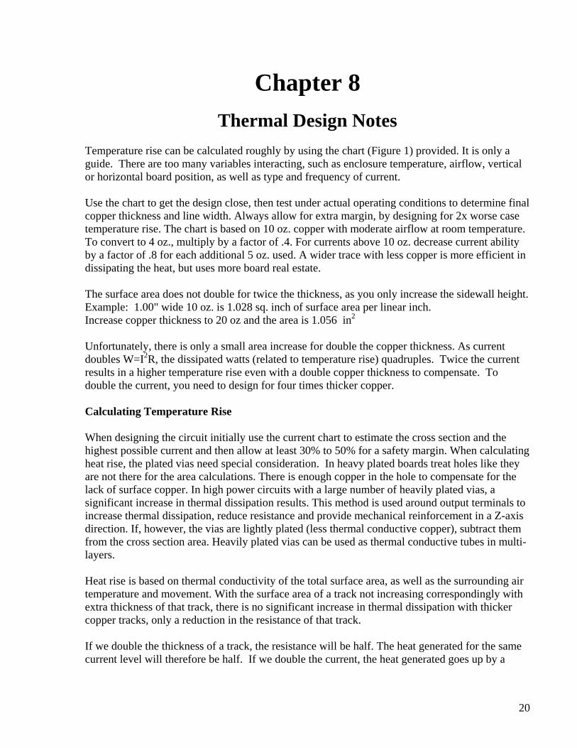
Thermal Design Notes Temperature rise can be calculated roughly by using the chart (Figure 1) provided. It is only a guide. There are too many variables interacting, such as enclosure temperature, airflow, vertical or horizontal board position, as well as type and frequency of current. Use the chart to get the design close, then test under actual operating conditions to determine final copper thickness and line width. Always allow for extra margin, by designing for 2x worse case temperature rise. The chart is based on 10 oz. copper with moderate airflow at room temperature. To convert to 4 oz., multiply by a factor of .4. For currents above 10 oz. decrease current ability by a factor of .8 for each additional 5 oz. used. A wider trace with less copper is more efficient in dissipating the heat, but uses more board real estate. The surface area does not double for twice the thickness, as you only increase the sidewall height. Example: 1.00" wide 10 oz. is 1.028 sq. inch of surface area per linear inch. Increase copper thickness to 20 oz and the area is 1.056 in2
Unfortunately, there is only a small area increase for double the copper thickness. As current doubles W=I2R, the dissipated watts (related to temperature rise) quadruples. Twice the current results in a higher temperature rise even with a double copper thickness to compensate. To double the current, you need to design for four times thicker copper. Calculating Temperature Rise When designing the circuit initially use the current chart to estimate the cross section and the highest possible current and then allow at least 30% to 50% for a safety margin. When calculating heat rise, the plated vias need special consideration. In heavy plated boards treat holes like they are not there for the area calculations. There is enough copper in the hole to compensate for the lack of surface copper. In high power circuits with a large number of heavily plated vias, a significant increase in thermal dissipation results. This method is used around output terminals to increase thermal dissipation, reduce resistance and provide mechanical reinforcement in a Z-axis direction. If, however, the vias are lightly plated (less thermal conductive copper), subtract them from the cross section area. Heavily plated vias can be used as thermal conductive tubes in multi-layers. Heat rise is based on thermal conductivity of the total surface area, as well as the surrounding air temperature and movement. With the surface area of a track not increasing correspondingly with extra thickness of that track, there is no significant increase in thermal dissipation with thicker copper tracks, only a reduction in the resistance of that track. If we double the thickness of a track, the resistance will be half. The heat generated for the same current level will therefore be half. If we double the current, the heat generated goes up by a
21
factor of four. To equal the temperature rise of a given circuit when the current is doubled, the thickness of the circuit traces would require an increase of thickness by four times. The type of laminate material used offers only a very small effect in a circuit's ability to carry current. The thermal conductivity of all the typically used material is similar. Larger thermal conductivity can be gained through the use of higher emissivity coating such as black oxide. Solder mask can also affect the circuit's ability to carry current. It is an electrical and thermal insulator. To increase thermal conductivity, the thinner the coating, the better. There are a few companies manufacturing thermally conductive epoxies. However, even those are relatively small gains as the conductivity is increased from .3 W/m°C to 4 W/m°C, a small increase from coppers huge conductivity of 320 W/m°C. The boron doped laminate is usually used to manufacture aluminum heavy copper circuits. Beware, sometimes the dielectric voltage rating drops after manufacturing and exposure to harsh environments to a very low level of 100 v/mill.
Line
Width Plated Copper
@ 80°C
Cross Sectional
Area
Temperature (°C) Increase Above Ambient vs.
No Air Flow Current (Amps)
(inch) (Ohms/ft) (mils2) 10° 20° 30° 40° .025 .031 337 4 6 9 10 .050 .015 675 6 10 12 13 .075 .010 1012 9 13 17 19 .100 .008 1350 11 16 19 21 .125 .006 1687 13 17 21 23 .250 .003 3375 22 35 40 45 .500 .0015 6750 40 68 74 80 .750 .0010 10125 60 90 110 120 1.000 .0009 13500 83 123 144 174
Figure 1: Temperature of 10 oz. Copper - Black oxide with solder mask, no air flow, enclosed case
“For Estimating Purposes Only”
22
Chapter 9
High Voltage Design Notes Heavy copper boards can operate in a high voltage condition, providing the standard design and construction rules are followed. When designing a heavy copper board for high voltage, be aware of the circuit spacing. High voltage creates shorts by two methods; direct arc over and corona. Arc over suddenly occurs when the voltage potential between two conductors exceeds the ionization value of the insulator between them. Dry air will arc over at approximately 10,000 volts per .250". Humid air will arc at as little as 5,000 volts per .250" with two sharp points. FR4 board material is rated around 350 volts per .001". HVPF from Sierra Proto Express has an aged dielectric breakdown rating of 3000 to 3500 volts per .001" thickness. The main culprit is corona; the invisible destructive force that slowly carbonizes the circuit board material. Corona is the ionization of the air and material immediately surrounding a high voltage circuit. It has an especially large effect if the high voltage conductor is sharp and pointed. Its potential damage increases with voltage and can be visually seen in very high voltage circuits as faint blue lightning like fingers coming forth from the surface. To minimize corona, the shape of the traces must be as round as possible. Avoid any sharp 90-degree bends. Make the traces flow with rounded corners. The soldering should be round and ball like, avoiding sharp pointed tips that enhance the corona effect. For double sided circuits, use as thick a board as you can, therefore giving you as much insulative material as possible between potentials. Space the high voltage circuits away from each other as much as physically possible. On multi-layers, the design should have as much room between the layers as you can. One flaw with heavy copper high voltage multi-layers is that the laminate does not press out fully without some air gaps and micro voids, which decrease the dielectric breakdown potential. On heavy copper multi-layers, the common practice is to specify multiple layers of prepreg to lessen the chance of a continuous void between heavy copper layers. To increase the dielectric strength between multi-layers use a single sheet of Sierra's HVPF material from .001" to .005" thick. As it is a film with no voids or holes, the rating is very high at over 3000v per mil. To further decrease the incidence of an arc over or the effects of corona, coat the board with two layers of solder mask. Again, two layers printed at cross-angles decreases the chance of a continuous pinhole or void. A UV cure bump and an extra solder mask bake further cures the solder mask and increases the dielectric value of the completed circuit. To assist in reducing the arc or corona effects of the completed circuit, a low temperature pre bake and a spray coat with one of the better conformal coatings will further improve the circuit's ability to withstand the ravishing effects of high voltage.
23
Chapter 10
Assembly and Connector Notes Assembly of heavy copper has some special problems for the design engineer. The very high heat sinking ability of 10 oz. of copper will prevent hand assembly with even a 100-watt iron. Heavy copper boards will however, solder well with a normal wave solder machine. For best results, slow the conveyor ever so slightly. To further assist the assembly process, use isothermal pads between solder points and the heavy copper traces. The lower copper mass around the lead transmits less heat to the heavy copper board, allowing the isothermal pad to heat up faster. These isothermal areas must be larger than normal because heavy copper imaging features less resolution. When assembling extra thick copper boards, some parts may require special soldering techniques. One customer uses resistance-welding equipment to heat up a stud for silver soldering onto the heavy copper surface. Most Pem nuts or studs are easily pushed into thick copper, providing excellent holding power. When large wires are to be soldered directly to the board, a large wattage iron of 200 watts may be required. Caution: the extra heat may damage the solder masks appearance. To reduce the damage from soldering, Sierra applies an oxide coating. This will provide as strong a solder mask as possible to stand up to the extra heat generated at assembly. When applying SMT components to mutil-level type boards where the power section is 10 oz. and the SMT part is 1 oz., you cannot use a screen printer to lay on the solder paste. It will not make proper contact in some areas because of the higher 10 oz. sections. You must use a CNC syringe paste dispenser. They are very common and should not be an issue. Or use a multilevel buried board where the copper traces are level with the surface. A standard IR oven profile is used; again, a slightly slower conveyor speed helps. Please don’t feel that the heavy copper needs a ton more heat and slow the conveyor to a crawl. You will damage the board. When using high current connectors, extra via holes in the area of the output connector increase thermal capacity and current carrying ability. Most importantly, they increase mechanical Z-axis compression resistance. Remember, fiberglass is a compressible material especially at elevated temperatures. Thick copper vias provide a strong, reasonably non-compressible mechanism to support the fiberglass and resist Z-axis compression over time. When the necessity arises to solder a thick copper buss or heat sink to a heavy copper board, you may have to preheat the part, then quickly assemble and solder. I have made soldering iron attachments that clamp on to the buss to keep the heat high enough to properly solder during the assembly phase and the applying of the solder. Care must be taken however, not to over heat the FR4 board, causing damage. The first sign of overheating is the FR4 will change color to a brown from a green; the darkness of the brown indicates the depth of the burn. Solder mask will start to soften and turn brown, if subjected to too much heat. The brown discoloration, if slight, is only
24
cosmetic. If the area is large or dark brown, it could indicate the FR4 is starting to carbonize and become conductive. You should not use this board. To properly insert Pem studs and nuts, a carefully sized hole will correctly anchor them when pushed in. The tolerance on the hole required is only -.0005" to + .001" .
Added Weight Any large connection method or larger components such as IGBT modules or large capacitors will add significant weight. Some designers use thicker fiberglass such as .093" or .125" to increase mechanical strength. Remember, a 10" x 12" board with 10 oz. of copper on both sides can easily weigh 2 lb. A larger quantity, or bigger than normal, mounting studs or flanges may be required to support the extra weight. Large wires attached to the board can provide unwanted side leveraging forces that can twist the board or break components. As most heavy copper designs require excessive currents to be carried (typically more than 300 amps), the problem becomes one of getting the high-current conductor connected to the board. Push-on terminals may not be able to handle the current.
This reduces the number of remaining alternatives. Using a nut-and-bolt combination, in a large pad area is usually disastrous, and is not recommended. The reason: excessive pressure created by a bolt and nut can distort the fiberglass and copper reducing pressure on the bolt causing a higher resistance joint with time and heat cycles. This, in turn, can overheat and cause failure.
The best connection method is to use PEM nuts that have been push fitted and soldered into a via reinforced plated-through hole. These allow the clampdown torque required for low-resistance electrical contact without stressing the board, allowing the engineer to design for larger connectors with PEM nut/bolts up to 3/8-in. diameter.
If you are using large bolts to carry the current, attention must be taken to ensure proper torque. Bellville washers help to maintain constant pressure. However, bolts are the least desirable method of carrying large currents. If you must use bolts, only use copper bolts, washers, nuts and preferably gold plated. Specify a torque value based on testing and demand it be followed. Add as many vias around the pad as possible to increase the Z-axis resistance to compression.
A third alternative is to directly solder the large clamped wires through the board, but this becomes impractical because of the large size of the wire involved and the excessive amount of heat required to make a good solder connection. Unless this large-diameter wire is effectively clamped to the board, mechanical stress in some situations can cause partial separation or damage to the copper on the board.
Elcon makes a reliable high current connector that solders or bolts directly to a heavy copper printed circuit board. I have used these connectors with excellent results. See www.elconproducts.com for details.
25
Chapter 11 Cost Considerations
The final and usually the most important consideration is the cost. This is not just the price of the board, but the reduced difference in the assembly costs and accessories of using a heavy copper board versus a typical 1 oz. printed circuit board and copper busses. Heavy copper printed circuit boards can be from 1.3 to 20 times more costly than comparable 1 oz. boards. There are many variables that will affect the final price. Ultimately, it's important to see whether a new design featuring heavy copper will save in overall cost and provide greater reliability. It must be compared to other methods that rely on conventional 1 oz. boards and thick machined copper buss bars soldered to the board or a heavy copper wire laid along the surface, then soldered. If these more “traditional” methods leave you cold, are too bulky, costly, unreliable, unsightly, or just won't fit into that tight-quarter avionics package, then it's time to look closely at boards with thick copper. Heavy copper boards are especially cost effective when they replace an entire box of wire, connectors, terminal blocks and assorted printed circuit boards. Heavy copper boards can significantly reduce the overall size and weight of the package as most components and wiring are on the board. The biggest cost benefit by far is the undeniable improvement in survivability heavy copper boards can realize over typical 1oz. circuits. What is the cost to your company in both reputation and financial burden to have a failed product in today's tough market place? A cost I cannot begin to, nor wish to calculate.
26
Chapter 12
Bendable Heavy Copper Circuits By combining a very particular property of epoxy and a certain thin weave of fiberglass, it results in a very bendable printed circuit board. It is, however, not flexible. By the term bendable, I mean that the circuit can conform to certain shapes mostly in one plane. A bendable circuit can withstand a small number of flex cycles, however, it is not designed to flex repeatedly. A properly designed and manufactured bendable circuit can bend as far as 360º in as little as 6 inches diameter. Some mechanical attachment device is needed to keep the circuit in the desired shape. Very heavy copper bendable circuits will retain a given shape, due to the mechanical retention nature of copper. Bendable circuits are used in applications where a flat, stiff circuit board will not fit. Typically, bendable circuits are single or double-sided circuits, with simple open designs. Crowded highly populated circuits do not bend well because the components do not bend. When designing a bendable board, consideration must be given to the placement of the components. All components must be kept clear of the bend lines. If only a small bend is required, some components such as capacitors will allow a very small radius. Multi-layers are possible but with limits on layer counts and the amount of bendability. As a multi-layer is a composite construction consisting of many layers, it imparts a stiffness in the inability of adjoining layers to move in relation to each other. One redeeming feature of bendable circuits is their lower cost compared to a typical double-sided heavy copper board. The laminate and the processing are considerably less expensive. Typical uses of a bendable circuit are the curved dash in an automobile, round sonar buoys, or connecting two power supplies of different heights. When a bendable board is used for a buss bar and plated with 10 oz. of copper, it will possess considerable strength. You can bend it into any shape and it will retain the shape due to the thickness of the copper.
27
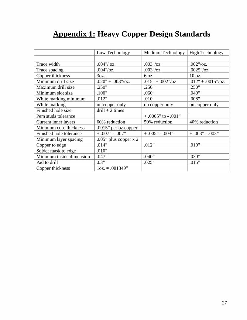
Appendix 1: Heavy Copper Design Standards Low Technology Medium Technology High Technology Trace width .004"/ oz. .003"/oz. .002"/oz. Trace spacing .004"/oz. .003"/oz. .0025"/oz. Copper thickness 3oz. 6 oz. 10 oz. Minimum drill size .020" + .003”/oz. .015" + .002”/oz .012" + .0015”/oz. Maximum drill size .250" .250" .250" Minimum slot size .100" .060" .040" White marking minimum .012" .010" .008" White marking on copper only on copper only on copper only Finished hole size drill + 2 times Pem studs tolerance + .0005” to - .001” Current inner layers 60% reduction 50% reduction 40% reduction Minimum core thickness .0015” per oz copper Finished hole tolerance + .007” - .007” + .005” - .004” + .003” - .003” Minimum layer spacing .005” plus copper x 2 Copper to edge .014" .012” .010” Solder mask to edge .010" Minimum inside dimension .047” .040” .030” Pad to drill .03” .025” .015” Copper thickness 1oz. = .001349”