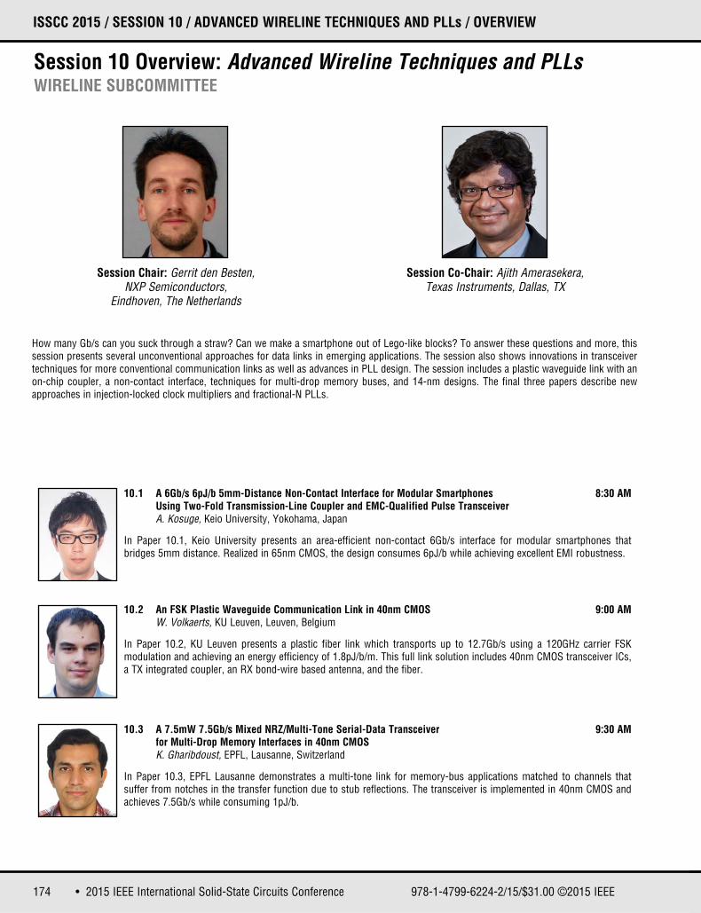
Session 10 Overview: Advanced Wireline Techniques and PLLs
29
174 • 2015 IEEE International Solid-State Circuits Conference 978-1-4799-6224-2/15/$31.00 ©2015 IEEE ISSCC 2015 / SESSION 10 / ADVANCED WIRELINE TECHNIQUES AND PLLs / OVERVIEW Session 10 Overview: Advanced Wireline Techniques and PLLs WIRELINE SUBCOMMITTEE 10.1 A 6Gb/s 6pJ/b 5mm-Distance Non-Contact Interface for Modular Smartphones 8:30 AM Using Two-Fold Transmission-Line Coupler and EMC-Qualified Pulse Transceiver A. Kosuge, Keio University, Yokohama, Japan In Paper 10.1, Keio University presents an area-efficient non-contact 6Gb/s interface for modular smartphones that bridges 5mm distance. Realized in 65nm CMOS, the design consumes 6pJ/b while achieving excellent EMI robustness. 10.2 An FSK Plastic Waveguide Communication Link in 40nm CMOS 9:00 AM W. Volkaerts, KU Leuven, Leuven, Belgium In Paper 10.2, KU Leuven presents a plastic fiber link which transports up to 12.7Gb/s using a 120GHz carrier FSK modulation and achieving an energy efficiency of 1.8pJ/b/m. This full link solution includes 40nm CMOS transceiver ICs, a TX integrated coupler, an RX bond-wire based antenna, and the fiber. 10.3 A 7.5mW 7.5Gb/s Mixed NRZ/Multi-Tone Serial-Data Transceiver 9:30 AM for Multi-Drop Memory Interfaces in 40nm CMOS K. Gharibdoust, EPFL, Lausanne, Switzerland In Paper 10.3, EPFL Lausanne demonstrates a multi-tone link for memory-bus applications matched to channels that suffer from notches in the transfer function due to stub reflections. The transceiver is implemented in 40nm CMOS and achieves 7.5Gb/s while consuming 1pJ/b. How many Gb/s can you suck through a straw? Can we make a smartphone out of Lego-like blocks? To answer these questions and more, this session presents several unconventional approaches for data links in emerging applications. The session also shows innovations in transceiver techniques for more conventional communication links as well as advances in PLL design. The session includes a plastic waveguide link with an on-chip coupler, a non-contact interface, techniques for multi-drop memory buses, and 14-nm designs. The final three papers describe new approaches in injection-locked clock multipliers and fractional-N PLLs. Session Chair: Gerrit den Besten, NXP Semiconductors, Eindhoven, The Netherlands Session Co-Chair: Ajith Amerasekera, Texas Instruments, Dallas, TX
-
Upload
khangminh22 -
Category
Documents
-
view
3 -
download
0
Transcript of Session 10 Overview: Advanced Wireline Techniques and PLLs
174 • 2015 IEEE International Solid-State Circuits Conference 978-1-4799-6224-2/15/$31.00 ©2015 IEEE
ISSCC 2015 / SESSION 10 / ADVANCED WIRELINE TECHNIQUES AND PLLs / OVERVIEW
Session 10 Overview: Advanced Wireline Techniques and PLLsWIRELINE SUBCOMMITTEE
10.1 A 6Gb/s 6pJ/b 5mm-Distance Non-Contact Interface for Modular Smartphones 8:30 AMUsing Two-Fold Transmission-Line Coupler and EMC-Qualified Pulse TransceiverA. Kosuge, Keio University, Yokohama, Japan
In Paper 10.1, Keio University presents an area-efficient non-contact 6Gb/s interface for modular smartphones thatbridges 5mm distance. Realized in 65nm CMOS, the design consumes 6pJ/b while achieving excellent EMI robustness.
10.2 An FSK Plastic Waveguide Communication Link in 40nm CMOS 9:00 AMW. Volkaerts, KU Leuven, Leuven, Belgium
In Paper 10.2, KU Leuven presents a plastic fiber link which transports up to 12.7Gb/s using a 120GHz carrier FSK modulation and achieving an energy efficiency of 1.8pJ/b/m. This full link solution includes 40nm CMOS transceiver ICs,a TX integrated coupler, an RX bond-wire based antenna, and the fiber.
10.3 A 7.5mW 7.5Gb/s Mixed NRZ/Multi-Tone Serial-Data Transceiver 9:30 AMfor Multi-Drop Memory Interfaces in 40nm CMOSK. Gharibdoust, EPFL, Lausanne, Switzerland
In Paper 10.3, EPFL Lausanne demonstrates a multi-tone link for memory-bus applications matched to channels that suffer from notches in the transfer function due to stub reflections. The transceiver is implemented in 40nm CMOS andachieves 7.5Gb/s while consuming 1pJ/b.
How many Gb/s can you suck through a straw? Can we make a smartphone out of Lego-like blocks? To answer these questions and more, thissession presents several unconventional approaches for data links in emerging applications. The session also shows innovations in transceivertechniques for more conventional communication links as well as advances in PLL design. The session includes a plastic waveguide link with anon-chip coupler, a non-contact interface, techniques for multi-drop memory buses, and 14-nm designs. The final three papers describe newapproaches in injection-locked clock multipliers and fractional-N PLLs.
Session Chair: Gerrit den Besten,NXP Semiconductors,
Eindhoven, The Netherlands
Session Co-Chair: Ajith Amerasekera, Texas Instruments, Dallas, TX
175DIGEST OF TECHNICAL PAPERS •
ISSCC 2015 / February 24, 2015 / 8:30 AM
10.4 A 5.8Gb/s Adaptive Integrating Duobinary-Based DFE Receiver 10:15 AMfor Multi-Drop Memory InterfaceH-W. Lim, Sungkyunkwan University, Suwon, Korea and Samsung Electronics, Hwaseong, Korea
In Paper 10.4, Sungkyunkwan University presents a duo-binary equalizing front-end for a binary link combined with a 5-tap DFE to adaptively remove pre- and post-cursor ISI without a high-boosting CTLE for reflective memory channelapplications. The DFE receiver implemented in 45nm CMOS operates at 5.8Gb/s and consumes 2.45pJ/b.
10.5 A 5.9pJ/b 10Gb/s Serial Link with Unequalized MM-CDR in 14nm Tri-Gate CMOS 10:45 AMR. Dokania, Intel, Hillsboro, OR
In Paper 10.5, Intel presents a 5.9pJ/b 10Gb/s serial link with improved lock-point Mueller-Müller CDR in 14nm tri-gateCMOS. The transceiver can work with 24dB channel loss, occupies 0.065mm2 and is 60% smaller than state-of-art comparable links.
10.6 Continuous-Time Linear Equalization with Programmable Active-Peaking Transistor 11:15 AMArrays in a 14nm FinFET 2mW/Gb/s 16Gb/s 2-Tap Speculative DFE ReceiverP. A. Francese, IBM Zurich, Rüschlikon, Switzerland
In Paper 10.6, IBM presents a 14nm FinFET 16Gb/s receiver with CTLE and 2-tap speculative DFE, capable of handling30dB channel loss and consuming 2pJ/b. The CTLE provides programmable active peaking with up to 8.8dB gain boostat 8GHz.
10.7 A 6.75-to-8.25GHz 2.25mW 190fsrms Integrated-Jitter PVT-Insensitive Injection-Locked 11:30 AMClock Multiplier Using All-Digital Continuous Frequency-Tracking Loop in 65nm CMOSA. Elkholy, University of Illinois, Urbana, IL
In Paper 10.7, University of Illinois presents a 65nm CMOS LC-based injection-locked clock multiplier from 6.75 to8.25GHz, achieving 190fsrms integrated jitter while consuming 2.25mW. The clock multiplier employs a digital frequency-tracking loop, ensuring robust operation across PVT variations.
10.8 A Wideband Fractional-N Ring PLL Using a Near-Ground 11:45 AMPre-Distorted Switched-Capacitor Loop FilterC-F. Liang, MediaTek, Hsinchu, Taiwan
In Paper 10.8, MediaTek presents a low-area fractional-N PLL in 40nm CMOS achieving fractional spurs below -70dBc andreference spurs below -87dBc. The PLL generates 2GHz from a 26MHz reference consuming 9.1mW. A switched-capacitorloop filter improves charge-pump noise and linearity and provides cancellation of ΔΣ modulator quantization noise.
10.9 A 13.1-to-28GHz Fractional-N PLL in 32nm SOI CMOS 12:00 PMwith a ΔΣ Noise-Cancellation SchemeM. Ferriss, IBM Research, Yorktown Heights, NY
In Paper 10.9, IBM presents a 13-to-28GHz hybrid analog/digital fractional-N PLL in 32nm CMOS SOI. The design employsa highly digital self-calibrating ΔΣ noise cancellation system to improve out-of-band phase noise significantly. The PLLoccupies 0.24mm2 and consumes 31mW.
10
176 • 2015 IEEE International Solid-State Circuits Conference
ISSCC 2015 / SESSION 10 / ADVANCED WIRELINE TECHNIQUES AND PLLs / 10.1
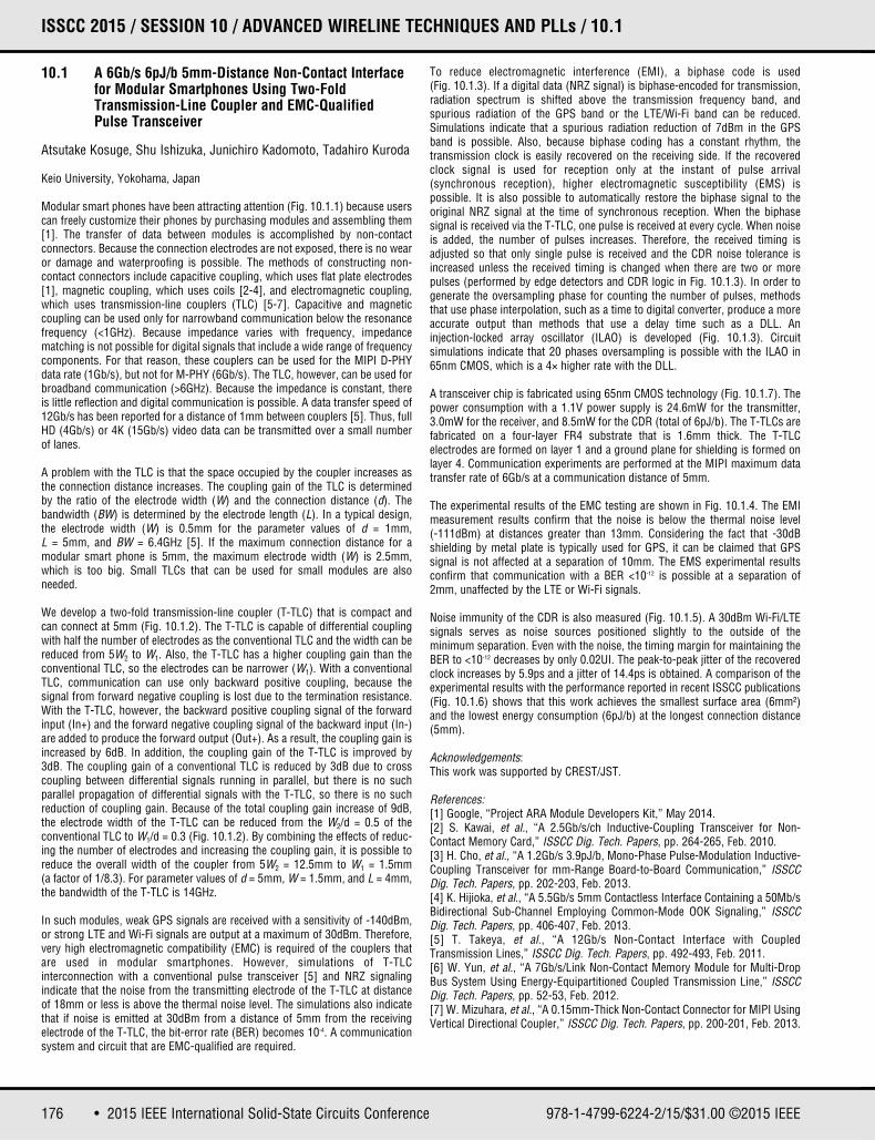
10.1 A 6Gb/s 6pJ/b 5mm-Distance Non-Contact Interface for Modular Smartphones Using Two-Fold Transmission-Line Coupler and EMC-Qualified Pulse Transceiver
Atsutake Kosuge, Shu Ishizuka, Junichiro Kadomoto, Tadahiro Kuroda
Keio University, Yokohama, Japan
Modular smart phones have been attracting attention (Fig. 10.1.1) because userscan freely customize their phones by purchasing modules and assembling them[1]. The transfer of data between modules is accomplished by non-contact connectors. Because the connection electrodes are not exposed, there is no wearor damage and waterproofing is possible. The methods of constructing non-contact connectors include capacitive coupling, which uses flat plate electrodes[1], magnetic coupling, which uses coils [2-4], and electromagnetic coupling,which uses transmission-line couplers (TLC) [5-7]. Capacitive and magneticcoupling can be used only for narrowband communication below the resonancefrequency (<1GHz). Because impedance varies with frequency, impedancematching is not possible for digital signals that include a wide range of frequencycomponents. For that reason, these couplers can be used for the MIPI D-PHYdata rate (1Gb/s), but not for M-PHY (6Gb/s). The TLC, however, can be used forbroadband communication (>6GHz). Because the impedance is constant, thereis little reflection and digital communication is possible. A data transfer speed of12Gb/s has been reported for a distance of 1mm between couplers [5]. Thus, fullHD (4Gb/s) or 4K (15Gb/s) video data can be transmitted over a small numberof lanes.
A problem with the TLC is that the space occupied by the coupler increases asthe connection distance increases. The coupling gain of the TLC is determinedby the ratio of the electrode width (W) and the connection distance (d). Thebandwidth (BW) is determined by the electrode length (L). In a typical design,the electrode width (W) is 0.5mm for the parameter values of d = 1mm,L = 5mm, and BW = 6.4GHz [5]. If the maximum connection distance for a modular smart phone is 5mm, the maximum electrode width (W) is 2.5mm,which is too big. Small TLCs that can be used for small modules are also needed.
We develop a two-fold transmission-line coupler (T-TLC) that is compact andcan connect at 5mm (Fig. 10.1.2). The T-TLC is capable of differential couplingwith half the number of electrodes as the conventional TLC and the width can bereduced from 5W2 to W1. Also, the T-TLC has a higher coupling gain than theconventional TLC, so the electrodes can be narrower (W1). With a conventionalTLC, communication can use only backward positive coupling, because the signal from forward negative coupling is lost due to the termination resistance.With the T-TLC, however, the backward positive coupling signal of the forwardinput (In+) and the forward negative coupling signal of the backward input (In-)are added to produce the forward output (Out+). As a result, the coupling gain isincreased by 6dB. In addition, the coupling gain of the T-TLC is improved by3dB. The coupling gain of a conventional TLC is reduced by 3dB due to crosscoupling between differential signals running in parallel, but there is no such parallel propagation of differential signals with the T-TLC, so there is no suchreduction of coupling gain. Because of the total coupling gain increase of 9dB,the electrode width of the T-TLC can be reduced from the W2/d = 0.5 of the conventional TLC to W1/d = 0.3 (Fig. 10.1.2). By combining the effects of reduc-ing the number of electrodes and increasing the coupling gain, it is possible toreduce the overall width of the coupler from 5W2 = 12.5mm to W1 = 1.5mm (a factor of 1/8.3). For parameter values of d = 5mm, W = 1.5mm, and L = 4mm,the bandwidth of the T-TLC is 14GHz.
In such modules, weak GPS signals are received with a sensitivity of -140dBm,or strong LTE and Wi-Fi signals are output at a maximum of 30dBm. Therefore,very high electromagnetic compatibility (EMC) is required of the couplers thatare used in modular smartphones. However, simulations of T-TLC interconnection with a conventional pulse transceiver [5] and NRZ signaling indicate that the noise from the transmitting electrode of the T-TLC at distanceof 18mm or less is above the thermal noise level. The simulations also indicatethat if noise is emitted at 30dBm from a distance of 5mm from the receiving electrode of the T-TLC, the bit-error rate (BER) becomes 10-4. A communicationsystem and circuit that are EMC-qualified are required.
To reduce electromagnetic interference (EMI), a biphase code is used(Fig. 10.1.3). If a digital data (NRZ signal) is biphase-encoded for transmission,radiation spectrum is shifted above the transmission frequency band, and spurious radiation of the GPS band or the LTE/Wi-Fi band can be reduced.Simulations indicate that a spurious radiation reduction of 7dBm in the GPSband is possible. Also, because biphase coding has a constant rhythm, the transmission clock is easily recovered on the receiving side. If the recoveredclock signal is used for reception only at the instant of pulse arrival (synchronous reception), higher electromagnetic susceptibility (EMS) is possible. It is also possible to automatically restore the biphase signal to theoriginal NRZ signal at the time of synchronous reception. When the biphase signal is received via the T-TLC, one pulse is received at every cycle. When noiseis added, the number of pulses increases. Therefore, the received timing isadjusted so that only single pulse is received and the CDR noise tolerance isincreased unless the received timing is changed when there are two or morepulses (performed by edge detectors and CDR logic in Fig. 10.1.3). In order togenerate the oversampling phase for counting the number of pulses, methodsthat use phase interpolation, such as a time to digital converter, produce a moreaccurate output than methods that use a delay time such as a DLL. An injection-locked array oscillator (ILAO) is developed (Fig. 10.1.3). Circuit simulations indicate that 20 phases oversampling is possible with the ILAO in65nm CMOS, which is a 4× higher rate with the DLL.
A transceiver chip is fabricated using 65nm CMOS technology (Fig. 10.1.7). Thepower consumption with a 1.1V power supply is 24.6mW for the transmitter,3.0mW for the receiver, and 8.5mW for the CDR (total of 6pJ/b). The T-TLCs arefabricated on a four-layer FR4 substrate that is 1.6mm thick. The T-TLC electrodes are formed on layer 1 and a ground plane for shielding is formed onlayer 4. Communication experiments are performed at the MIPI maximum datatransfer rate of 6Gb/s at a communication distance of 5mm.
The experimental results of the EMC testing are shown in Fig. 10.1.4. The EMImeasurement results confirm that the noise is below the thermal noise level (-111dBm) at distances greater than 13mm. Considering the fact that -30dBshielding by metal plate is typically used for GPS, it can be claimed that GPS signal is not affected at a separation of 10mm. The EMS experimental resultsconfirm that communication with a BER <10-12 is possible at a separation of2mm, unaffected by the LTE or Wi-Fi signals.
Noise immunity of the CDR is also measured (Fig. 10.1.5). A 30dBm Wi-Fi/LTEsignals serves as noise sources positioned slightly to the outside of the minimum separation. Even with the noise, the timing margin for maintaining theBER to <10-12 decreases by only 0.02UI. The peak-to-peak jitter of the recoveredclock increases by 5.9ps and a jitter of 14.4ps is obtained. A comparison of theexperimental results with the performance reported in recent ISSCC publications(Fig. 10.1.6) shows that this work achieves the smallest surface area (6mm²)and the lowest energy consumption (6pJ/b) at the longest connection distance(5mm).
Acknowledgements: This work was supported by CREST/JST.
References: [1] Google, “Project ARA Module Developers Kit,” May 2014.[2] S. Kawai, et al., “A 2.5Gb/s/ch Inductive-Coupling Transceiver for Non-Contact Memory Card,” ISSCC Dig. Tech. Papers, pp. 264-265, Feb. 2010.[3] H. Cho, et al., “A 1.2Gb/s 3.9pJ/b, Mono-Phase Pulse-Modulation Inductive-Coupling Transceiver for mm-Range Board-to-Board Communication,” ISSCCDig. Tech. Papers, pp. 202-203, Feb. 2013.[4] K. Hijioka, et al., “A 5.5Gb/s 5mm Contactless Interface Containing a 50Mb/sBidirectional Sub-Channel Employing Common-Mode OOK Signaling,” ISSCCDig. Tech. Papers, pp. 406-407, Feb. 2013.[5] T. Takeya, et al., “A 12Gb/s Non-Contact Interface with CoupledTransmission Lines,” ISSCC Dig. Tech. Papers, pp. 492-493, Feb. 2011.[6] W. Yun, et al., “A 7Gb/s/Link Non-Contact Memory Module for Multi-DropBus System Using Energy-Equipartitioned Coupled Transmission Line,” ISSCCDig. Tech. Papers, pp. 52-53, Feb. 2012.[7] W. Mizuhara, et al., “A 0.15mm-Thick Non-Contact Connector for MIPI UsingVertical Directional Coupler,” ISSCC Dig. Tech. Papers, pp. 200-201, Feb. 2013.
978-1-4799-6224-2/15/$31.00 ©2015 IEEE
177DIGEST OF TECHNICAL PAPERS •
ISSCC 2015 / February 24, 2015 / 8:30 AM
Figure 10.1.1: Non-contact interface for modular smartphone. Figure 10.1.2: Two-fold transmission-line coupler (T-TLC).
Figure 10.1.3: Biphase pulse transceiver and noise tolerant pulse CDR.
Figure 10.1.5: Measured BER bathtub curves and recovered clock jitters. Figure 10.1.6: Performance comparison.
Figure 10.1.4: Measured electromagnetic compatibility (EMC).
10

• 2015 IEEE International Solid-State Circuits Conference 978-1-4799-6224-2/15/$31.00 ©2015 IEEE
ISSCC 2015 PAPER CONTINUATIONS
Figure 10.1.7: Micrographs of transceiver chip and photographs of the T-TLC.
178 • 2015 IEEE International Solid-State Circuits Conference
ISSCC 2015 / SESSION 10 / ADVANCED WIRELINE TECHNIQUES AND PLLs / 10.2
10.2 An FSK Plastic Waveguide CommunicationLink in 40nm CMOS
Wouter Volkaerts, Niels Van Thienen, Patrick Reynaert
KU Leuven, Leuven, Belgium
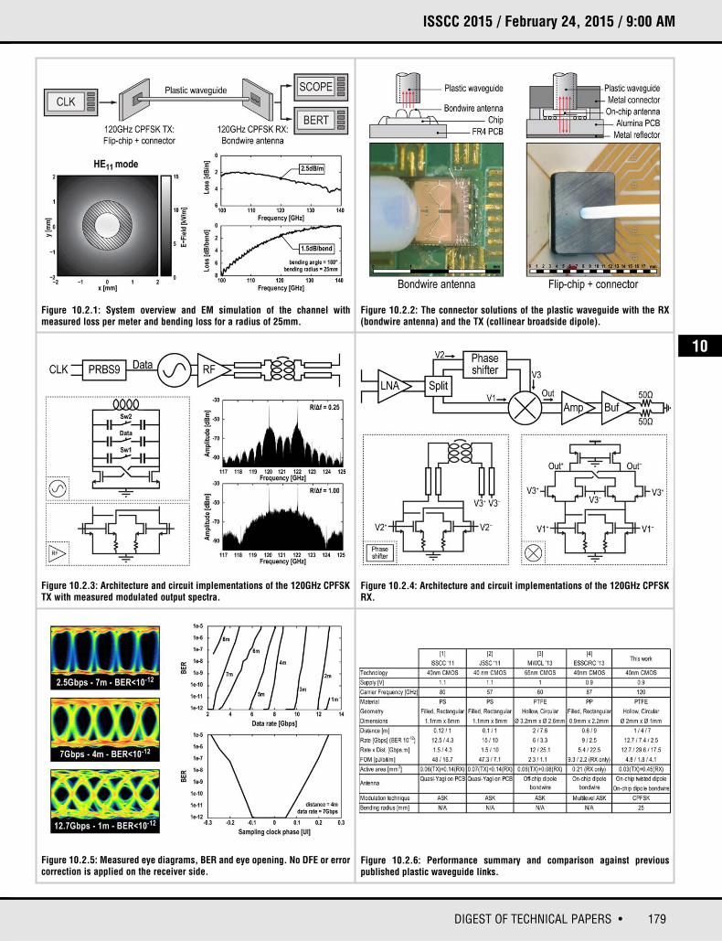
Technology scaling has enabled RF-CMOS circuits that operate in the millimeter-wave frequency range (30 to 300GHz) where large bandwidths are available.These bandwidths can be exploited to increase data-rates of wireless communication links. Unfortunately, free-space path loss (FSPL) limits the operating distance of wireless systems at these frequencies. A 5-meter link at120GHz has an FSPL as high as 88dB. Therefore such wireless links are feasibleonly with highly directive antennas. This work uses a directive channel instead.At mm-Wave frequencies, the directive channel can be a low-cost plastic fiber orhollow tube, made from PP, PS or Teflon. These directive channels will guideelectromagnetic waves with low loss from TX to RX [1-4]. As such, RF communication through a plastic fiber becomes an interesting alternative andcomplements existing solutions like wireline copper or optical fibers. This paperpresents an entire communication link that uses a continuous-phase frequency-shift keying (CPFSK) TX and RX. We report on 120GHz 40nm CMOSTX and RX chips, the connector solution, and the plastic channel. Data-rates upto 12.7Gb/s over 1m, transmission lengths up to 7m at 2.5Gb/s and an energyefficiency of 1.8pJ/b/m for 4m and 7.4Gb/s are achieved for the complete com-munication link. All these results are for a BER 10-12. Compared to previous work,measurements also show the link still works for a bending radius of only 25mm,thanks to the selection of a high carrier frequency.
The system architecture is shown in Figure 10.2.1. The CPFSK transmitter modulates PRBS9 input data on a 120GHz carrier and radiates the RF output signal into a plastic waveguide. An on-chip antenna in the CPFSK receiver picksup the signal and demodulates it to baseband. Because of the large bandwidthavailable at 120GHz, a simple modulation scheme can be used to reach a highdata-rate. CPFSK modulation is chosen for its robustness and low implementation complexity for both transmitter and receiver circuitry and constant envelope RF signals, which results in low power consumption. The useof mm-Wave carrier frequencies enables the integration of on-chip antennas.However, this can cause frequency pulling of the oscillator in the transmitter,which degrades the performance of phase-modulated systems, like BPSK orQPSK. The CPFSK modulator is immune against this pulling because the frequency jumps caused by the modulation are chosen much larger than theones caused by the pulling. The selection of 120GHz as carrier frequency ismainly driven by the small bending radius of 25mm and 1.5dB loss for a 180°bend. To guide the 120GHz carrier, a hollow Teflon tube of 2mm outer and 1mminner diameter is used. The channel has a measured loss of 2.5dB per meter at120GHz.
In this work, both a bondwire dipole antenna and an on-chip collinear broadsidedipole with backside radiation are implemented on chip, to couple the 120GHzmodulated RF signal into the plastic waveguide (see Figure 10.2.2). A bondwiredipole antenna is straightforward and gives good coupling into the plastic waveguide. This implementation is excellent for testing purposes. The secondantenna is a collinear broadside dipole implemented in the top metal layer of the40nm CMOS chip. This implementation is flip-chipped on a substrate with areflector and the RF output signal is radiated by the backside of the chip. A metalconnector, in which the waveguide can be inserted, is glued to the substrate andforms a robust connection between the backside of the chip and the fiber withoutextra losses. An important advantage compared to optical communication is therelaxed mechanical alignment requirement between the plastic fiber and theantenna. The output power varies only 2dB when moving the waveguide 0.5mmoff-center in H-plane or E-plane of the antenna.
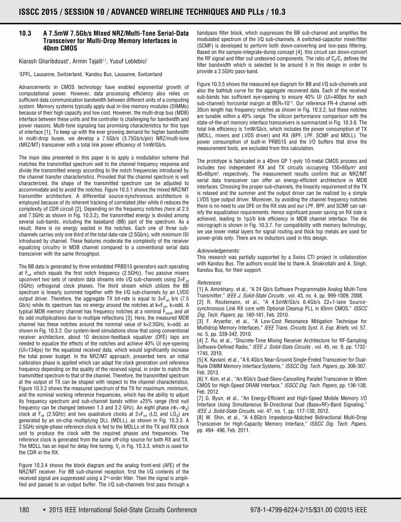
Figure 10.2.3 presents the architecture of the transmitter. The 120GHz CPFSKtransmitter includes an embedded PRBS9 generator for testing the link. ThisPRBS9 data modulates the frequency of a digital controlled oscillator. The oscillator, implemented by a cross-coupled pair and an LC-tank, generates the120GHz carrier. Three switched capacitors are used in the tank, one causes frequency jumps of 4GHz for the modulation and the two other give a 2GHz frequency shift each. The 120GHz output buffer is implemented as a differentialpair with neutralization gate-drain capacitors and amplifies the VCO signal.Transmission lines and a transformer perform the impedance match between
this buffer and the antenna. The power consumption is 6.5mW and 4.5mW forthe oscillator and output buffer, respectively. Figure 10.2.3 also shows twomeasured spectra of the modulated 120GHz output of the transmitter. In the bottom and top spectrum the modulation index (R/Δf) is 1 and 0.25, respectively. For transmitter output measurements, the RF output is radiated intoa plastic waveguide that is connected to a harmonic mixer for down-conversion.The losses of the setup are not de-embedded in the spectra.
The architecture of the CPFSK receiver is shown in Fig. 10.2.4. The LNA amplifies the incoming signal of the antenna, the demodulator retrieves the baseband signal that is amplified by the post-amplifier, and the measurementbuffer is used to drive the 50Ω measurement equipment. The 120GHz LNA has5 stages with a total gain of 26.8dB, a noise figure of 6.6dB and a power consumption of 28.7mW. Each stage consists of a neutralized differential pairand a matching network. The S-curve CPFSK demodulator consists of a splitter,a phase shifter and a mixer. The mm-Wave phase shifter is implemented as atuned amplifier and the mixer as a Gilbert cell. The demodulation is performedby creating frequency-dependent phase shifts between the two input signals ofthe mixer, which results in voltage jumps at the output. This avoids the need forpower hungry LO generation. Besides a large frequency to phase gain, the phaseshifter is designed to match the optimal DC phase difference at the input of themixer. The power consumption of the demodulator is only 4mW. The post-amplifier and the measurement buffer consist of 6 stages in total. The firsttwo stages consume 8.3mW and are designed small to minimize the load to themixer and achieve a high bandwidth. The other four stages consume 48.2mWand are optimized to drive an off-chip 50Ω load. In three stages inductive peaking is used to enhance the bandwidth of both the post-amplifier and themeasurement buffer and to compensate for the filtering effect of the bondwiresneeded to bring the baseband signal off-chip. The power consumption of thepost-amplifier is included in the FOM calculations.
The measurements of the full link are presented in Fig. 10.2.5. The CPFSK transmitter requires only a DC connection and a clock for the PRBS data generation. The 120GHz CPFSK modulated signal is sent through the plasticwaveguide, demodulated in the receiver and visualized on a scope or measuredwith a BERT (ParBERT 81250). The measured BER and eye diagrams for different data-rates and distances are given. No decision-feedback equalizationor error correction is applied in the measurements. For a BER of 10-12 the longestdistance is 7m with a data-rate of 2.5Gb/s and the highest data-rate is 12.7Gb/sover 1m. The best FOM with BER 10-12 is 1.8pJ/b/m and is achieved for a 4mplastic link with a 7.4Gb/s data-rate. The measured bathtub curve shows an eyeopening of 0.14UI at BER 10-12 for 7Gb/s over a 4m fiber. For a distance of 4mand a data-rate of 7.4Gb/s, the power consumption of the entire communicationlink is 52mW, of which 11mW in the transmitter and 41mW in the receiver.
Figure 10.2.6 compares the results against previously published communicationlinks with plastic waveguides. The carrier frequency used in this work is higherthan previous presented implementations to allow a short bending radius. Theachieved bit rates are competitive for both short and long distance, while thiswork achieves higher product of data-rate and distance. The chips are implemented in a 40nm CMOS technology and die micrographs are shown inFig. 10.2.7. The active area is 0.45mm² in the receiver and 0.03mm² in the transmitter. The antenna occupies 1mm² in the receiver and 0.81mm² in thetransmitter.
References:[1] S. Fukuda, et al., “A 12.5+12.5 Gb/s Full-Duplex Plastic WaveguideInterconnect,” ISSCC Dig. Tech. Papers, pp. 150-151, Feb. 2011.[2] S. Fukuda, et al., “A 12.5+12.5 Gb/s Full-Duplex Plastic WaveguideInterconnect,” IEEE J. Solid-State Circuits, vol. 46, no. 12, pp. 3113-3125, Dec.2011.[3] Y. Kim, et al., “High-Speed mm-Wave Data-Link Based on Hollow PlasticCable and CMOS Transceiver,” IEEE Microwave and Wireless ComponentsLetters, vol. 23, no. 12, pp. 674-676, Dec. 2013.[4] M. Tytgat, et al., “A plastic waveguide receiver in 40nm CMOS with on-chipbondwire antenna,” Proc. ESSCIRC 2013, pp. 335-338, Sept. 2013.
978-1-4799-6224-2/15/$31.00 ©2015 IEEE
179DIGEST OF TECHNICAL PAPERS •
ISSCC 2015 / February 24, 2015 / 9:00 AM
Figure 10.2.1: System overview and EM simulation of the channel with measured loss per meter and bending loss for a radius of 25mm.
Figure 10.2.2: The connector solutions of the plastic waveguide with the RX(bondwire antenna) and the TX (collinear broadside dipole).
Figure 10.2.3: Architecture and circuit implementations of the 120GHz CPFSKTX with measured modulated output spectra.
Figure 10.2.5: Measured eye diagrams, BER and eye opening. No DFE or errorcorrection is applied on the receiver side.
Figure 10.2.6: Performance summary and comparison against previous published plastic waveguide links.
Figure 10.2.4: Architecture and circuit implementations of the 120GHz CPFSKRX.
10

• 2015 IEEE International Solid-State Circuits Conference 978-1-4799-6224-2/15/$31.00 ©2015 IEEE
ISSCC 2015 PAPER CONTINUATIONS
Figure 10.2.7: Die micrograph of TX (flip-chip) and RX (bondwire).
180 • 2015 IEEE International Solid-State Circuits Conference
ISSCC 2015 / SESSION 10 / ADVANCED WIRELINE TECHNIQUES AND PLLs / 10.3
10.3 A 7.5mW 7.5Gb/s Mixed NRZ/Multi-Tone Serial-Data Transceiver for Multi-Drop Memory Interfaces in 40nm CMOS
Kiarash Gharibdoust1, Armin Tajalli1,2, Yusuf Leblebici1
1EPFL, Lausanne, Switzerland, 2Kandou Bus, Lausanne, Switzerland
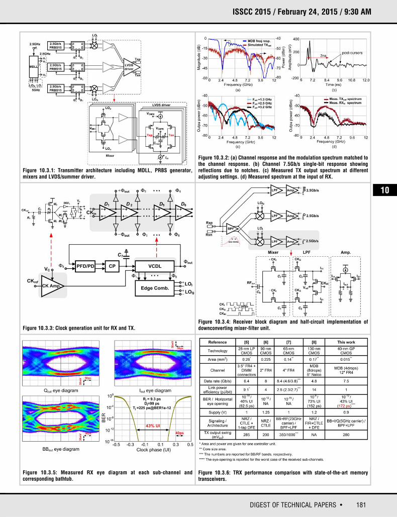
Advancements in CMOS technology have enabled exponential growth of computational power. However, data processing efficiency also relies on sufficient data communication bandwidth between different units of a computingsystem. Memory systems typically apply dual in-line memory modules (DIMMs)because of their high capacity and low cost. However, the multi-drop bus (MDB)interface between these units and the controller is challenging for bandwidth andpower reasons. Multi-tone signaling has promising characteristics for this typeof interface [1]. To keep up with the ever growing demand for higher bandwidthin multi-drop buses, we develop a 7.5Gb/s (3.75Gb/s/pin) NRZ/multi-tone(NRZ/MT) transceiver with a total link power efficiency of 1mW/Gb/s.
The main idea presented in this paper is to apply a modulation scheme thatmatches the transmitted spectrum well to the channel frequency response anddivide the transmitted energy according to the notch frequencies introduced bythe channel transfer characteristics. Provided that the channel spectrum is wellcharacterized, the shape of the transmitted spectrum can be adjusted to accommodate and to avoid the notches. Figure 10.3.1 shows the mixed NRZ/MTtransmitter architecture. A differential source-synchronous architecture isemployed because of its inherent tracking of correlated jitter while it reduces thecomplexity of CDR circuit [2]. Depending on the frequency notches (here at 2.5and 7.5GHz as shown in Fig. 10.3.2), the transmitted energy is divided amongseveral sub-bands, including the baseband (BB) part of the spectrum. As aresult, there is no energy wasted in the notches. Each one of three sub-channels carries only one third of the total data-rate (2.5Gb/s), with minimum ISIintroduced by channel. These features moderate the complexity of the receiverequalizing circuitry in MDB channel compared to a conventional serial datatransceiver with the same throughput.
The BB data is generated by three embedded PRBS15 generators each operatingat Fref which equals the first notch frequency (2.5GHz). Two passive mixersupconvert two sets of random data streams into I/Q sub-channels using 2×Fref
(5GHz) orthogonal clock phases. The third stream which utilizes the BB spectrum is linearly summed together with the I/Q sub-channels by an LVDSoutput driver. Therefore, the aggregate TX bit-rate is equal to 3×Fref b/s (7.5Gb/s) while its spectrum has no energy around the notches at k×Fref, k=odd. Atypical MDB memory channel has frequency notches at a nominal Fnotch and allits odd multiplications due to multiple reflections [3]. Here, the measured MDBchannel has these notches around the nominal value of k×2.5GHz, k=odd, asshown in Fig. 10.3.2. Our system-level simulations show that using conventionalreceiver architecture, about 10 decision-feedback equalizer (DFE) taps are needed to equalize the effects of the notches and achieve 40% UI eye-opening(UI=134ps) for the equalized received data, which would significantly increasethe total power budget. In the NRZ/MT approach, presented here, an initial calibration phase is applied which can adapt the clock generation unit referencefrequency depending on the quality of the received signal, in order to match thetransmitted spectrum to that of the channel. Therefore, the transmitted spectrumat the output of TX can be shaped with respect to the channel characteristics.Figure 10.3.2 shows the measured spectrum of the TX for maximum, minimum,and the nominal working reference frequencies, which has the ability to adjustits frequency spectrum and sub-channel bands within ±25% range (first null frequency can be changed between 1.3 and 3.2 GHz). An eight phase (Φ1−Φ8)clock at Fref (2.5GHz) and two quadrature clocks at 2×Fref (LOI and LOQ) are generated by an on-chip multiplying DLL (MDLL), as shown in Fig. 10.3.3. A2.5GHz single-phase reference clock is fed to the MDLLs of the TX and RX clockunit to produce the clock with the required phases and frequencies. The reference clock is generated from the same off-chip source for both RX and TX.The MDLL has an input for delay fine tuning, Vc in Fig. 10.3.3, which is used forthe CDR in the RX.
Figure 10.3.4 shows the block diagram and the analog front-end (AFE) of theNRZ/MT receiver. For BB sub-channel reception, first the I/Q contents of thereceived signal are suppressed using a 2nd-order filter. Then the signal is ampli-fied and passed to an output buffer. The I/Q sub-channels first pass through a
bandpass filter block, which suppresses the BB sub-channel and amplifies themodulated spectrum of the I/Q sub-channels. A switched-capacitor mixer/filter(SCMF) is developed to perform both down-converting and low-pass filtering.Based on the sample-integrate-dump concept [4], this circuit can down-convertthe RF signal and filter out undesired components. The ratio of C2/C1 defines thefilter bandwidth which is selected to be around 5 in this design in order to provide a 2.5GHz pass-band.
Figure 10.3.5 shows the measured eye diagram for BB and I/Q sub-channels andalso the bathtub curve for the aggregate recovered data. Each of the receivedsub-bands has sufficient eye-opening to ensure 40% UI (UI=400ps for each sub-channel) horizontal margin at BER=10-12. Our reference FR-4 channel with30cm length has frequency notches as shown in Fig. 10.3.2, but these notchesare tunable within a 40% range. The silicon performance comparison with the state-of-the-art memory interface transceivers is summarized in Fig. 10.3.6. Thetotal link efficiency is 1mW/Gb/s, which includes the power consumption of TX(MDLL, mixers and LVDS driver) and RX (BPF, LPF, SCMF and MDLL). Thepower consumption of built-in PRBS15 and the I/O buffers that drive the measurement tools, are excluded from this calculation.
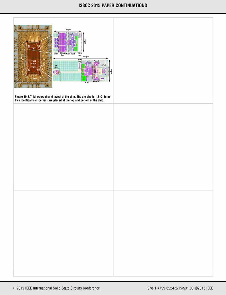
The prototype is fabricated in a 40nm GP 1-poly 10-metal CMOS process andincludes two independent RX and TX circuits occupying 150×60μm2 and85×60μm2, respectively. The measurement results confirm that an NRZ/MT serial data transceiver can offer an energy-efficient architecture in MDB interfaces. Choosing the proper sub-channels, the linearity requirement of the TXis relaxed and the summer and the output driver can be realized by a simpleLVDS type output driver. Moreover, by avoiding the channel frequency notchesthere is no need to use DFE on the RX side and our LPF, BPF, and SCMF can sat-isfy the equalization requirements. Hence significant power saving on RX side isachieved, leading to 1pJ/b link efficiency in MDB channel interface. The diemicrograph is shown in Fig. 10.3.7. For compatibility with memory technology,we use lower metal layers for signal routing and thick top metals are used forpower-grids only. There are no inductors used in this design.
Acknowledgements:This research was partially supported by a Swiss CTI project in collaborationwith Kandou Bus. The authors would like to thank A. Shokrollahi and A. Singh,Kandou Bus, for their support.
References:[1] A. Amirkhany, et al., “A 24 Gb/s Software Programmable Analog Multi-ToneTransmitter,” IEEE J. Solid-State Circuits , vol. 43, no. 4, pp. 999-1009, 2008.[2] R. Reutemann, et al., “A 4.5mW/Gb/s 6.4Gb/s 22+1-lane Source-synchronous Link RX core with Optional Cleanup PLL in 65nm CMOS,” ISSCCDig. Tech. Papers, pp. 160-161, Feb. 2010.[3] F. Aryanfar, et al., “A Low-Cost Resonance Mitigation Technique forMultidrop Memory Interfaces,” IEEE Trans. Circuits Syst. II, Exp. Briefs, vol. 57,no. 5, pp. 339-342, 2010.[4] Z. Ru, et al., “Discrete-Time Mixing Receiver Architecture for RF-SamplingSoftware-Defined Radio,” IEEE J. Solid-State Circuits , vol. 45, no. 9, pp. 1732-1745, 2010.[5] K. Kaviani, et al., “A 6.4Gb/s Near-Ground Single-Ended Transceiver for Dual-Rank DIMM Memory Interface Systems,” ISSCC Dig. Tech. Papers, pp. 306-307,Feb. 2013.[6] Y. Kim, et al., “An 8Gb/s Quad-Skew-Cancelling Parallel Transceiver in 90nmCMOS for High-Speed DRAM Interface,” ISSCC Dig. Tech. Papers, pp. 136-138,Feb. 2012.[7] G. Byun, et al., “An Energy-Efficient and High-Speed Mobile Memory I/OInterface Using Simultaneous Bi-Directional Dual (Base+RF)-Band Signaling,”IEEE J. Solid-State Circuits, vol. 47, no. 1, pp. 117-130, 2012. [8] W. Shin, et al., “A 4.8Gb/s Impedance-Matched Bidirectional Multi-DropTransceiver for High-Capacity Memory Interface,” ISSCC Dig. Tech. Papers,pp. 494- 496, Feb. 2011.
978-1-4799-6224-2/15/$31.00 ©2015 IEEE
181DIGEST OF TECHNICAL PAPERS •
ISSCC 2015 / February 24, 2015 / 9:30 AM
Figure 10.3.1: Transmitter architecture including MDLL, PRBS generator, mixers and LVDS/summer driver.
Figure 10.3.2: (a) Channel response and the modulation spectrum matched tothe channel response. (b) Channel 7.5Gb/s single-bit response showingreflections due to notches. (c) Measured TX output spectrum at differentadjusting settings. (d) Measured spectrum at the input of RX.
Figure 10.3.3: Clock generation unit for RX and TX.
Figure 10.3.5: Measured RX eye diagram at each sub-channel and corresponding bathtub.
Figure 10.3.6: TRX performance comparison with state-of-the-art memorytransceivers.
Figure 10.3.4: Receiver block diagram and half-circuit implementation ofdownconverting mixer-filter unit.
10
• 2015 IEEE International Solid-State Circuits Conference 978-1-4799-6224-2/15/$31.00 ©2015 IEEE
ISSCC 2015 PAPER CONTINUATIONS
Figure 10.3.7: Micrograph and layout of the chip. The die size is 1.3×2.8mm2.Two identical transceivers are placed at the top and bottom of the chip.
182 • 2015 IEEE International Solid-State Circuits Conference
ISSCC 2015 / SESSION 10 / ADVANCED WIRELINE TECHNIQUES AND PLLs / 10.4
10.4 A 5.8Gb/s Adaptive Integrating Duobinary-Based DFE Receiver for Multi-Drop Memory Interface
Hyun-Wook Lim1,2, Sung-Won Choi1,2, Sang-Kyu Lee2, Chang-Hoon Baek2, Jae-Youl Lee2, Gyoo-Cheol Hwang2, Bai-Sun Kong1, Young-Hyun Jun2
1Sungkyunkwan University, Suwon, Korea, 2Samsung Electronics, Hwaseong, Korea
Emerging applications like cloud computing require high-speed low-latencyaccess to high-volume data. In these applications, use of memory modules having multi-drop channels may be needed for time-efficient access to high-density memory data. A key design issue here is how to let interface transceiversnot be affected by ISI and reflection noise generated by multi-drop channels having imperfect termination. The current-integrating decision-feedback equalizer (DFE) [1], which can cancel both high-frequency noise and post-cursorISI simultaneously, has a limitation due to high gain-boosting and/or tap weightover-emphasis in equalizers to avoid eye closure caused by ISI-referred inputpattern dependency. Duobinary signaling [2], which requires less boosting forequalizers by taking advantage of channel roll-off characteristic, is not effectivein a multi-drop channel application because even a small timing or waveformvariation due to high-frequency noise may cause degradation of the quality ofduobinary signals. This work presents an integrating duobinary-based DFEreceiver to avoid drawbacks described above and to increase the effective-datarate of multi-drop channels. A synergistic combination between the integratingequalizer and the duobinary signaling can provide advantages such as 1) lowergain-boosting for equalizers, 2) no need for precursor equalization, 3) ideally noinput-pattern dependency during integration, 4) being more robust to high-frequency noise, 5) alleviated DFE critical timing, and 6) embedding DFE tapsinto duobinary circuits.
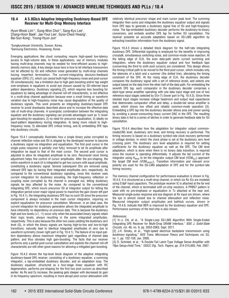
Figure 10.4.1 conceptually illustrates how a single binary pulse corrupted bychannel reflection noise and ISI is shaped by the developed receiver to becomea duobinary signal via integration and equalization. The first post cursor in thesingle pulse response is partially (not fully) removed to let its amplitude afterintegration be equal to that of the main cursor. The second post cursor is adjusted to allow its integrated amplitude to be zero. Recovered clock timingadjustment helps fine control of cursor amplitudes. After the pre-shaping, theentire waveform in each UI is integrated to get two cursors with equal amplitude,constituting a duobinary signal. Several subsequent ISIs are removed using relevant DFE taps by having their integrated amplitudes zero, respectively. Ascompared to the conventional duobinary signaling, since this receiver uses current integration for duobinary encoding, the high-frequency reflection or coupling noise corrupted by the channel is averaged out, letting duobinary signals be less affected by the noise. As compared to the conventional integrating DFE, which incurs precursor ISI at integrator output for letting theintegration period cover major signal power to maximize the gain (lower left partin Fig. 10.4.1), the integrating duobinary DFE has no such ISI since the precursorcomponent is always included in the main cursor integration, requiring noexplicit equalization for precursor cancellation. Moreover, in an ideal case, thecurrent integration for duobinary generation allows the integrated amplitude tohave inherently no dependency on previous data. This is because the duobinaryhigh and low levels (+1, -1) occur only when the associated binary signals retaintheir logic levels, always resulting in the same integrated amplitudes, respectively. This is also because the other two cases yielding the duobinary zerolevel (0), in which the binary signals are having high-to-low and low-to-hightransitions, naturally lead to identical integrated amplitudes of zero due to waveform symmetry (lower right part in Fig. 10.4.1). The feature of no input-pat-tern dependency allows maximum integrator gain regardless of channel datapattern, and thus obviates high gain-boosting. The facts that our receiver performs only a partial post-cursor cancellation and exploits the channel roll-offcharacteristic are still other good reasons for allowing a mitigated gain boosting.
Figure 10.4.2 shows the top-level block diagram of the adaptive integratingduobinary-based DFE receiver, consisting of a duobinary equalizer, a summingintegrator, a tap-embedded duobinary decoder, and an adaptation loop. Theduobinary equalizer, structured as a four-stage linear equalizer with RC degeneration, performs pre-shaping for the first two post cursors as describedearlier. As Rs and Cs increase, the peaking gets steeper with decreased dc gainin its frequency spectrum, resulting in more abrupt post cursor attenuation with
relatively identical precursor shape and main cursor peak level. The summingintegrator then sums and integrates the duobinary equalizer output and signalsfrom DFE taps to generate a duobinary signal free of ISI and high-frequencynoise. The tap-embedded duobinary decoder performs the duobinary-to-binaryconversion, and embeds another DFE tap for further ISI cancellation. The receiver presents an accurate adaptation based on SS-LMS algorithm by extracting transition information from the duobinary signal.
Figure 10.4.3 shows a detailed block diagram for the half-rate integrating duobinary DFE. Differential signaling is employed for the benefits in improvingcrosstalk, simultaneous switching noise, and common-mode noise rejection. Atthe falling edge of CLK, the even data-path starts current summing and integration, where the duobinary equalizer output and four feedback taps (concerning the third to sixth post cursors) are considered. This design allowsthe timing-critical path to be moved to the third post cursor, which includes onlythe latencies of a latch and a summer (the dotted line), alleviating the timing constraint of the DFE. At the rising edge of CLK, the duobinary decoder compares the duobinary signal with a set of reference levels, and selects oneoutput based on the data from the other half of the data path. For embedding theseventh DFE tap, each comparator in the duobinary decoder comprises a latch-type sense amplifier operating with one data input stage and one of tworeference input stages selected by D(n-7) (lower part in Fig. 10.4.3). Since threestacked input stages increase voltage headroom and output load capacitancethat deteriorates comparator offset and delay, a double-tail sense amplifier isused, which shows low offset and reliable common-mode operation [3].Embedding a DFE tap into the duobinary decoder allows area and power savingby avoiding a power-consuming heavy current DAC in the DFE. The resultingbinary data is fed to a series of latches in order to generate feedback data for ISIcancellation.
Figure 10.4.4 describes how the adaptation for integrator output common-mode(CM) level, duobinary zero level, and timing recovery is performed. Thetiming recovery is based on a duobinary symbol-rate clock recovery performedin voltage domain, in which the clock phase is set at the duobinary zero levelcrossing point. The duobinary zero level adaptation is required for setting coefficients for the duobinary equalizer as well as the DFE. The CM level adaptation, which is done when there is no binary data transition, is requiredsince the receiver is operating differentially. It adjusts the tail current of the integrator using HMAIN to let the integrator output CM level (VCMOUT) approachthe target CM level (VCMTARGET). Transition information and relevant error polarity are used for the SS-LMS adaptation of DFE and for the symbol-rate timing recovery.
The memory channel configuration for performance evaluation is shown in Fig.10.4.5. It is structured as a multi-drop channel, in which six Rx ICs are modeledusing 0.9pF input capacitors. The prototype receiver IC is attached at the far endof the channel, which is terminated with on-chip resistors. A PRBS7 pattern isused with no pre-emphasis or equalization in Tx attached at the near end.Measured single-pulse response and eye diagram at Rx input are shown, wherethe eye is almost closed due to channel attenuation and reflection noise.Measured integrator output amplitudes and bathtub curves, shown inFig. 10.4.6, indicate that BER is improved by the duobinary equalizer and DFE.Performance summary of the test-chip is also shown.
References:[1] H.-J. Chi, et al., “A Single-Loop SS-LMS Algorithm With Single-EndedIntegrating DFE Receiver for Multi-Drop DRAM Interface,” IEEE J. Solid-StateCircuits, vol. 46, no. 9, pp. 2053-2063, Sept. 2011.[2] J.H. Sinsky, et al., “High-speed electrical backplane transmission usingduobinary signaling,” IEEE Trans. Microwave Theory and Techniques, vol. 53,no. 1, pp. 152-159, Jan. 2005.[3] D. Schinkel, et al., “A Double-Tail Latch-Type Voltage Sense Amplifier with18ps Setup+Hold Time,” ISSCC Dig. Tech. Papers, pp. 314-315,605, Feb. 2007.
978-1-4799-6224-2/15/$31.00 ©2015 IEEE
183DIGEST OF TECHNICAL PAPERS •
ISSCC 2015 / February 24, 2015 / 10:15 AM
Figure 10.4.1: Concept of integrating duobinary-based DFE.Figure 10.4.2: Top block diagram of adaptive integrating duobinary-based DFEreceiver.
Figure 10.4.3: Half-rate integrating duobinary equalizer with decision feed-back.
Figure 10.4.5: Test environment and measured signal integrity.Figure 10.4.6: Measured integrator output amplitudes, measured bathtubcurves, and performance summary.
Figure 10.4.4: Integrator structure and adaptation algorithm.
10

• 2015 IEEE International Solid-State Circuits Conference 978-1-4799-6224-2/15/$31.00 ©2015 IEEE
ISSCC 2015 PAPER CONTINUATIONS
Figure 10.4.7: Chip micrograph.
184 • 2015 IEEE International Solid-State Circuits Conference
ISSCC 2015 / SESSION 10 / ADVANCED WIRELINE TECHNIQUES AND PLLs / 10.5
10.5 A 5.9pJ/b 10Gb/s Serial Link with Unequalized MM-CDR in 14nm Tri-Gate CMOS
Rajeev Dokania1, Alexandra Kern1, Mike He2, Adam Faust1, Richard Tseng1, Skyler Weaver1, Kai Yu1, Christiaan Bil3, Tao Liang3, Frank O’Mahony1
1Intel, Hillsboro, OR, 2Intel, Santa Clara, CA, 3Intel, Hudson, MA
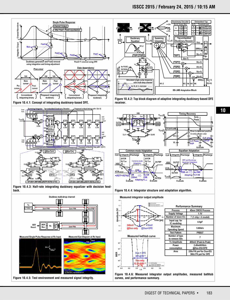
High-speed serial links integrated in advanced CMOS are ubiquitous in modernmicroprocessor systems. These commodity links have fixed performance specsand therefore realize the benefit of technology scaling in area and power reduction at high data rates. To realize significant scaling benefits, these designsmust overcome the challenges associated with implementing analog functions inscaled logic-optimized processes while maintaining link robustness over a widerange of channel characteristics and third party components.
This work describes a 2.5-to-10 Gb/s serial link implemented in 14nm tri-gateCMOS using logic-pitch transistors exclusively. The half-rate embedded-clocktransceiver architecture (Fig. 10.5.1) [1] consists of a 3-tap current-mode (CM)TX, an RX with a CTLE, a 4-tap integrating DFE, and a phase-interpolator-basedCDR. It is 60% smaller and consumes 11% less energy per bit than reportedlinks at comparable data rates and channel losses. It also introduces a baud-rateCDR algorithm that uses the real-time extracted channel response at the DFE tooptimize the sampling point, relaxes the headroom/swing tradeoff at the TX driver by using dynamic signal boosting, eliminates the process cost for a precision resistor by using tunable serpentine resistors, and includes a low-power and low-area RX squelch circuit with a digital peak detector.
The CM TX (Fig. 10.5.2) consists of multiple unit current-switching elements(legs) and incorporates several design features to enable robust performance ina deep submicron CMOS technology with limited voltage headroom. With a target output swing of 1Vppdiff (AC coupled 0.25 to 0.75V) and a supply voltageof 0.9V, headroom limitations make achieving symmetric equalization levels andmeeting the AC common-mode requirements with a conventional CM driver difficult. To address this, additional legs are dynamically switched in based onthe data pattern to provide a swing boost. In parallel with the 63 main driver legs,up to 9 additional balance legs are selectively enabled at the peak equalizationlevel to provide a swing boost that compensates for headroom-induced currentcompression.
To minimize process cost and circuit complexity, the resistors used for the TXand RX terminations are implemented in an existing interconnect layer withoutany resistor-specific processing. The resistance of this layer is not well definedduring early process development, resulting in a wide design window. Designingfor this full window would have added significant pad capacitance and circuitarea. Instead, the resistors are constructed using a serpentine structure, allowing a simple layout edit to change the target resistance late in the processdevelopment without pin/port changes. Due to this tunable resistor, the designskew window is comparable to a precision resistor using dedicated masks, butwithout additional cost to the process.
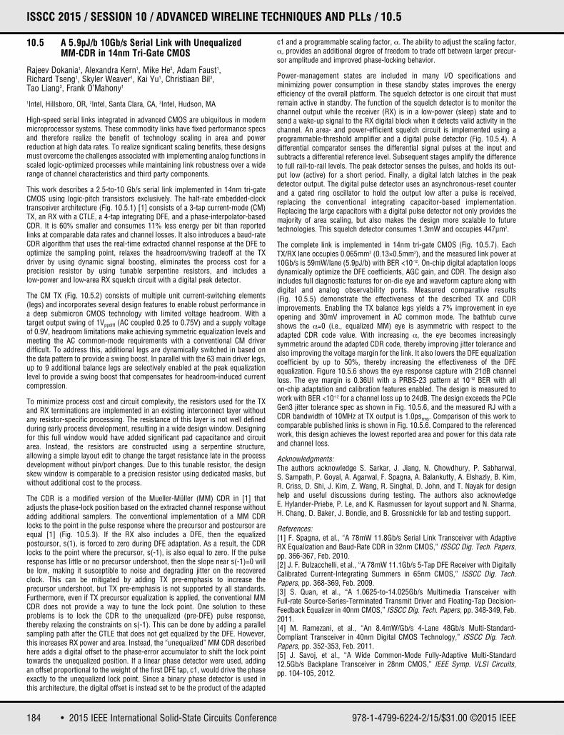
The CDR is a modified version of the Mueller-Müller (MM) CDR in [1] thatadjusts the phase-lock position based on the extracted channel response withoutadding additional samplers. The conventional implementation of a MM CDRlocks to the point in the pulse response where the precursor and postcursor areequal [1] (Fig. 10.5.3). If the RX also includes a DFE, then the equalized postcursor, s(1), is forced to zero during DFE adaptation. As a result, the CDRlocks to the point where the precursor, s(-1), is also equal to zero. If the pulseresponse has little or no precursor undershoot, then the slope near s(-1)=0 willbe low, making it susceptible to noise and degrading jitter on the recoveredclock. This can be mitigated by adding TX pre-emphasis to increase the precursor undershoot, but TX pre-emphasis is not supported by all standards.Furthermore, even if TX precursor equalization is applied, the conventional MMCDR does not provide a way to tune the lock point. One solution to these problems is to lock the CDR to the unequalized (pre-DFE) pulse response, thereby relaxing the constraints on s(-1). This can be done by adding a parallelsampling path after the CTLE that does not get equalized by the DFE. However,this increases RX power and area. Instead, the “unequalized” MM CDR describedhere adds a digital offset to the phase-error accumulator to shift the lock pointtowards the unequalized position. If a linear phase detector were used, addingan offset proportional to the weight of the first DFE tap, c1, would drive the phaseexactly to the unequalized lock point. Since a binary phase detector is used inthis architecture, the digital offset is instead set to be the product of the adapted
c1 and a programmable scaling factor, α. The ability to adjust the scaling factor,α, provides an additional degree of freedom to trade off between larger precur-sor amplitude and improved phase-locking behavior.
Power-management states are included in many I/O specifications and minimizing power consumption in these standby states improves the energy efficiency of the overall platform. The squelch detector is one circuit that mustremain active in standby. The function of the squelch detector is to monitor thechannel output while the receiver (RX) is in a low-power (sleep) state and tosend a wake-up signal to the RX digital block when it detects valid activity in thechannel. An area- and power-efficient squelch circuit is implemented using aprogrammable-threshold amplifier and a digital pulse detector (Fig. 10.5.4). Adifferential comparator senses the differential signal pulses at the input and subtracts a differential reference level. Subsequent stages amplify the differenceto full rail-to-rail levels. The peak detector senses the pulses, and holds its out-put low (active) for a short period. Finally, a digital latch latches in the peakdetector output. The digital pulse detector uses an asynchronous-reset counterand a gated ring oscillator to hold the output low after a pulse is received, replacing the conventional integrating capacitor-based implementation.Replacing the large capacitors with a digital pulse detector not only provides themajority of area scaling, but also makes the design more scalable to future technologies. This squelch detector consumes 1.3mW and occupies 447μm2.
The complete link is implemented in 14nm tri-gate CMOS (Fig. 10.5.7). EachTX/RX lane occupies 0.065mm2 (0.13×0.5mm2), and the measured link power at10Gb/s is 59mW/lane (5.9pJ/b) with BER <10-12. On-chip digital adaptation loopsdynamically optimize the DFE coefficients, AGC gain, and CDR. The design alsoincludes full diagnostic features for on-die eye and waveform capture along withdigital and analog observability ports. Measured comparative results(Fig. 10.5.5) demonstrate the effectiveness of the described TX and CDRimprovements. Enabling the TX balance legs yields a 7% improvement in eyeopening and 30mV improvement in AC common mode. The bathtub curveshows the α=0 (i.e., equalized MM) eye is asymmetric with respect to the adapted CDR code value. With increasing α, the eye becomes increasingly symmetric around the adapted CDR code, thereby improving jitter tolerance andalso improving the voltage margin for the link. It also lowers the DFE equalizationcoefficient by up to 50%, thereby increasing the effectiveness of the DFE equalization. Figure 10.5.6 shows the eye response capture with 21dB channelloss. The eye margin is 0.36UI with a PRBS-23 pattern at 10-12 BER with all on-chip adaptation and calibration features enabled. The design is measured towork with BER <10-12 for a channel loss up to 24dB. The design exceeds the PCIeGen3 jitter tolerance spec as shown in Fig. 10.5.6, and the measured RJ with aCDR bandwidth of 10MHz at TX output is 1.0psrms. Comparison of this work tocomparable published links is shown in Fig. 10.5.6. Compared to the referencedwork, this design achieves the lowest reported area and power for this data rateand channel loss.
Acknowledgments:The authors acknowledge S. Sarkar, J. Jiang, N. Chowdhury, P. Sabharwal, S. Sampath, P. Goyal, A. Agarwal, F. Spagna, A. Balankutty, A. Elshazly, B. Kim,R. Criss, D. Shi, J. Kim, Z. Wang, R. Singhal, D. John, and T. Nayak for designhelp and useful discussions during testing. The authors also acknowledge E. Hylander-Priebe, P. Le, and K. Rasmussen for layout support and N. Sharma,H. Chang, D. Baker, J. Bondie, and B. Grossnickle for lab and testing support.
References:[1] F. Spagna, et al., “A 78mW 11.8Gb/s Serial Link Transceiver with AdaptiveRX Equalization and Baud-Rate CDR in 32nm CMOS,” ISSCC Dig. Tech. Papers,pp. 366-367, Feb. 2010.[2] J. F. Bulzacchelli, et al., “A 78mW 11.1Gb/s 5-Tap DFE Receiver with DigitallyCalibrated Current-Integrating Summers in 65nm CMOS,” ISSCC Dig. Tech.Papers, pp. 368-369, Feb. 2009.[3] S. Quan, et al., “A 1.0625-to-14.025Gb/s Multimedia Transceiver with Full-rate Source-Series-Terminated Transmit Driver and Floating-Tap Decision-Feedback Equalizer in 40nm CMOS,” ISSCC Dig. Tech. Papers, pp. 348-349, Feb.2011.[4] M. Ramezani, et al., “An 8.4mW/Gb/s 4-Lane 48Gb/s Multi-Standard-Compliant Transceiver in 40nm Digital CMOS Technology,” ISSCC Dig. Tech.Papers, pp. 352-353, Feb. 2011.[5] J. Savoj, et al., “A Wide Common-Mode Fully-Adaptive Multi-Standard12.5Gb/s Backplane Transceiver in 28nm CMOS,” IEEE Symp. VLSI Circuits,pp. 104-105, 2012.
978-1-4799-6224-2/15/$31.00 ©2015 IEEE
185DIGEST OF TECHNICAL PAPERS •
ISSCC 2015 / February 24, 2015 / 10:45 AM
Figure 10.5.1: Link Architecture.Figure 10.5.2: Transmitter balance leg circuit architecture and operation toboost swing and reduce AC common-mode variation.
Figure 10.5.3: Unequalized MM CDR operating principle.
Figure 10.5.5: Measured TX waveforms with balance legs and RX bathtubcurves with equalized and unequalized MM CDR.
Figure 10.5.6: Results showing jitter tolerance compliance for PCI Gen3, RXcaptured eye at 10Gb/s over 21dB channel, and a comparison of this work tocomparable published links.
Figure 10.5.4: Area- and power-efficient squelch circuit implementation.
10
• 2015 IEEE International Solid-State Circuits Conference 978-1-4799-6224-2/15/$31.00 ©2015 IEEE
ISSCC 2015 PAPER CONTINUATIONS
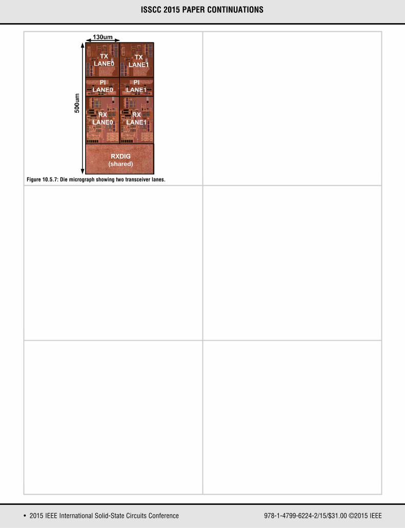
Figure 10.5.7: Die micrograph showing two transceiver lanes.
186 • 2015 IEEE International Solid-State Circuits Conference
ISSCC 2015 / SESSION 10 / ADVANCED WIRELINE TECHNIQUES AND PLLs / 10.6
10.6 Continuous-Time Linear Equalization with Programmable Active-Peaking Transistor Arrays in a 14nm FinFET 2mW/Gb/s 16Gb/s 2-Tap Speculative DFE Receiver
Pier Andrea Francese, Thomas Toifl, Matthias Braendli, Christian Menolfi, Marcel Kossel, Thomas Morf, Lukas Kull, Toke Meyer Andersen, Hazar Yueksel, Alessandro Cevrero, Danny Luu
IBM Zurich, Rüschlikon, Switzerland
We report the implementation of a continuous-time linear equalizer (CTLE) featuring a new technique to control the high-frequency gain peaking and tointerface to current-summing stages usually implemented as interleaved slicesfor the linear analog superposition of the coefficients of decision-feedback equalizers (DFE). The circuits are implemented in 14nm FinFET SOI CMOS technology and are included in a prototype receiver targeted to 16Gb/s serial I/Olinks for multi-core microprocessors off-chip communication. The architectureis shown in Fig. 10.6.1. Power efficiency and compactness are among the primary goals of the study together with an equalization capability sufficient torecover at bit-error rate (BER) levels below 10-12 data transmitted across smoothchannels with losses in excess of 25dB at 8GHz.
To achieve the required equalization range we combined frequency-dependentsource-degeneration with a programmable array of active peaking transistorsfollowed by interleaved integrating summers also implemented as a programmable transistor array. The conceptual schematic of the solution isshown in Fig. 10.6.2. Active peaking has been previously used in I/Oreceivers [1]. In our contribution the key innovative element lies in the ability tocontrol both the high-frequency peaking gain and the integrating summer gainby means of switches connected directly to the power rail. The avoidance of control switches connected between the power rails is advantageous when lowsupply voltages are used and when the switches are located along high-frequency analog signal paths. The active peaking transistor array is subdividedinto half sections. The first half array comprises transistors connected as diodes,whereas the second half consists of transistors with a single resistor RPEAKconnecting the gates to the drains. The switches at the sources are controlled tomaintain a constant number of transistors turned on in the array so that everyelement operates at the same current density. When the peaking control selectsall the transistors of the first half, the impedance of the active load is given bythe parallel of diode-connected transistors. Therefore, with respect to the integrating summer, a current-mirroring function is obtained with no unwantedpeaking. When all the transistors of the second half are selected, the current mirroring characteristic is present only in the low-frequency part of the spectrum. At high frequencies the RPEAK decouples the gates from the drains sothat the transistors act as current sources and the signal at the integrating summer input is amplified. By selecting only complementary fractions of the twohalf sections of the array the amount of peaking is modulated. The basic small-signal equivalent schematic and analysis are shown in Fig. 10.6.3. The calculated curves provide insight into the maximum magnitude of gain peakingthat may be achieved as a function of the active peaking control n, which is fundamentally limited by the self-gain gm2/go2 of the transistors.
The simplified schematic of the receiver analog data path is shown in Fig. 10.6.4.The active peaking transistor array is connected to a PMOS source-degenerateddifferential pair. Such a telescopic connection is particularly power-efficientbecause two peaking circuits are powered with the same current branch. The frequency-dependent source-degeneration peaking is designed to equalize atquarter baud-rate, whereas the active peaking is designed for half baud-rate. Thepassive linear equalizer, which also sets the common-mode (CM) voltage at thePMOS differential pair inputs, is sized for further equalization in the lower frequency part of the spectrum. The gate-to-drain parasitic capacitance of theactive peaking transistors reduces the decoupling effect of RPEAK and is thereforedifferentially cancelled with matching cross-coupled transistors. The current-integrating summer requires a calibration procedure to set the CM voltage at its outputs. The ratio of the current mirroring between the active peaking and integrating summer arrays is set at startup. On a finer level, current-steering DACs are programmed to trim the CM voltage precisely to275mV below the supply rail. After such CM calibration the data-path differentialgain is tolerant to process and temperature variations when sufficient resistive
degeneration is implemented and if a bias current is derived from the ratio of avoltage reference and a resistor of the same type as in the degeneration.
The gain peaking of the active transistor array is measured at half baud-rate fromthe amplitudes reached at the comparator inputs when a repetitive 1010 patternis received. The two measurements shown in Fig. 10.6.5 are at minimum and atmaximum DC gain. The measured gain peaking at 8GHz is 8.8 and 8.3dB,respectively. The additional gain peaking from the passive linear equalizer andthe source-degeneration is sufficient to exceed our 10dB target. The 0.5dB difference is due to the gain compression and represents a measure of the linearity of the data path at half baud-rate. Measurements at DC show 0.6dBsmall-signal gain and 1dB gain compression at 702mVppdiff input amplitude,which translates to 670mVppdiff at the comparator inputs.
There is a tradeoff between the maximum amount of active peaking and the sensitivity target. High values of the peaking resistor are sought to achieve themaximum amount of gain peaking. However the peaking-resistor thermal-noisecontribution may become dominant and either a lower resistor value preferredor more stages used in parallel at the expense of a lower power efficiency. Thesensitivity of the receiver analog data path is measured at the minimum and themaximum active peaking setting to evaluate its noise contribution. The sensitivity is derived as the standard deviation of the normal distribution fittingthe cumulative distribution functions of one comparator output collected byvarying its threshold voltage. The standard deviation increased from 3.68 to4.23mVrms. As a signal at half baud-rate is amplified by at least 8.3dB and themeasured sensitivity penalty is 1.2dB, we conclude that we achieve a signal-to-noise ratio improvement of 7.1dB due to the active peaking.
The receiver includes a 2-tap speculative DFE and its equalization combined withthe CTLE is sufficient for recovering 900mVppdiff data transmitted without feed-forward equalization across a PCB channel with 30dB loss at 8GHz. The BERbathtub curves are shown in Fig. 10.6.6. The horizontal eye margins with 4∙1012
bits checked are 10 and 5 phase rotator steps out of the 32 covering one unitinterval (UI) for PRBS test sequences of order 7 and 31, respectively. The twopost-cursors H1 and H2 DFE coefficients are optimally set in the center of theerror-free area of a BER scan and the CTLE peaking controls are set to maximum.
At 16Gb/s the total current drawn from the single 900mV power supply voltageis 36.4mA, which translates to 2.04mW/Gb/s power efficiency. According tosimulation the power consumption of the CTLE alone is 2.16mW. Correct functionality is verified up to 20Gb/s and at that speed the efficiency improves to1.93mW/Gb/s. In a system-on-chip implementation the power efficiency isexpected to improve further owing to the power consumption amortization ofshared circuits such as the clock receiver and the digital correlator.
The micrograph of the test circuit is displayed in Fig. 10.6.7. The physical layoutsof the implemented telescopic PMOS differential pair, active peaking transistorarray and integrating summer array are highlighted together with their dimensions in the 14nm FinFET CMOS technology used. With respect to prior art[2-4] with short DFEs our receiver, which benefits from the active peaking boost,exhibits superior equalization capability of channel losses at half baud-rate and the lowest CTLE power consumption when implemented.
Acknowledgement:The authors wish to thank the foundry team in IBM Fishkill, NY, for the circuits’fabrication, Dan Dreps, IBM Austin, TX and Steven Baumgartner, IBM Rochester,MN, for the valuable inputs and support.
References:[1] E. Sackinger and W. Fischer, “A 3 GHz, 32 dB CMOS Limiting Amplifier forSONET OC-48 Receivers,” ISSCC Dig. Tech. Papers, pp. 158-159, Feb. 2000.[2] K. Jung, et al., “A 0.94mW/Gb/s 22Gb/s 2-Tap Partial-Response DFEReceiver in 40nm LP CMOS,” ISSCC Dig. Tech. Papers, pp. 42-44, Feb. 2013.[3] R. Bai, et al., “A 0.25pJ/b 0.7V 16Gb/s 3-Tap Decision-Feedback Equalizer in65nm CMOS,” ISSCC Dig. Tech. Papers, pp. 46-48, Feb. 2014.[4] J.W. Jung and B. Razavi, “25Gb/s 5.8mW CMOS Equalizer,” ISSCC Dig.Tech. Papers, pp. 44-46, Feb. 2014.
978-1-4799-6224-2/15/$31.00 ©2015 IEEE
187DIGEST OF TECHNICAL PAPERS •
ISSCC 2015 / February 24, 2015 / 11:15 AM
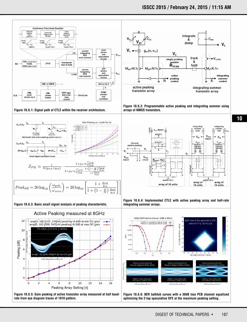
Figure 10.6.1: Signal path of CTLE within the receiver architecture.Figure 10.6.2: Programmable active peaking and integrating summer usingarrays of NMOS transistors.
Figure 10.6.3: Basic small signal analysis of peaking characteristic.
Figure 10.6.5: Gain peaking of active transistor array measured at half baud-rate from eye diagram traces of 1010 pattern.
Figure 10.6.6: BER bathtub curves with a 30dB loss PCB channel equalizedoptimizing the 2-tap speculative DFE at the maximum peaking setting.
Figure 10.6.4: Implemented CTLE with active peaking array and half-rate integrating summer arrays.
10
• 2015 IEEE International Solid-State Circuits Conference 978-1-4799-6224-2/15/$31.00 ©2015 IEEE
ISSCC 2015 PAPER CONTINUATIONS
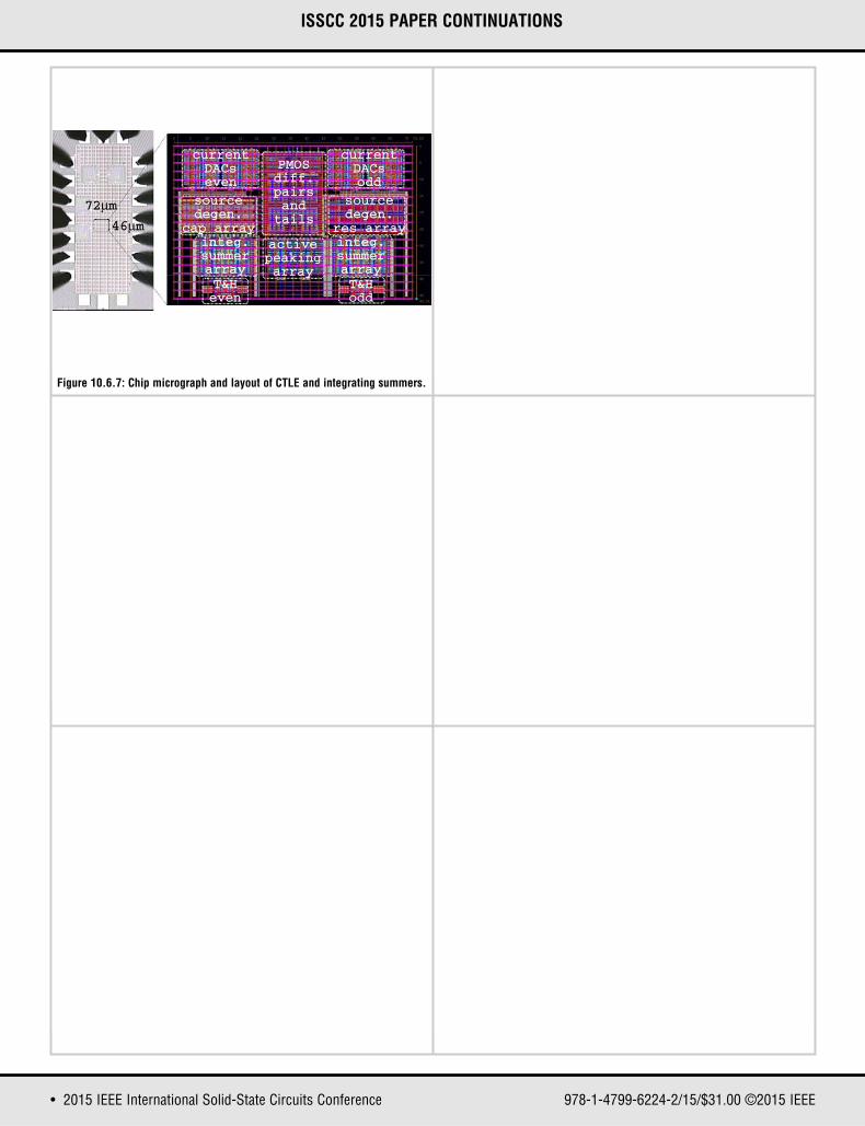
Figure 10.6.7: Chip micrograph and layout of CTLE and integrating summers.
188 • 2015 IEEE International Solid-State Circuits Conference
ISSCC 2015 / SESSION 10 / ADVANCED WIRELINE TECHNIQUES AND PLLs / 10.7
10.7 A 6.75-to-8.25GHz 2.25mW 190fsrms Integrated-Jitter PVT-Insensitive Injection-Locked Clock Multiplier Using All-Digital Continuous Frequency-Tracking Loop in 65nm CMOS
Ahmed Elkholy, Mrunmay Talegaonkar, Tejasvi Anand, Pavan Kumar Hanumolu
University of Illinois, Urbana, IL
Sub-harmonically injection locked oscillators provide a simple means for generating very-low-noise high-frequency clocks in a power, and area efficientmanner [1-5]. Ideally, a free-running oscillator can be locked to the Nth harmonicof a reference clock simply by injecting narrow pulses at reference frequency(FREF) into the oscillator, such that FOUT=NFREF. In the locked state, the oscillatortracks the reference clock and its close-in phase noise is greatly suppressed. Assuch, the phase noise of an injection-locked clock multiplier (ILCM) is limitedonly by the noise of reference clock. However, in practice, there are severaldesign challenges that limit usage of ILCMs. First, lock-in range (ΔFL) of theinjection-locked oscillator is limited. Therefore, separate frequency tuning, typically performed using a phase-locked loop (PLL) is needed to bring the oscillator free-running frequency (FFR) to be within the lock-in range, i.e., FERR= FFR-NFREF<ΔFL [5]. If FERR≠ 0 (but <ΔFL), injection ensures phase locking butcauses a reference spur whose magnitude is proportional to FERR [1]. The secondmajor challenge is the voltage and temperature (VT) sensitivity of ILCM. FERR
increases as FFR drifts due to VT variations, which degrades phase noise andspurious performance and may even lead to loss of lock once FERR exceeds ΔFL
[4]. This is especially problematic in the case of high-Q LC oscillators becauseof their relatively small ΔFL. Techniques to extend ΔFL by reducing N or loweringQ are undesirable as smaller N mandates higher FREF and lower Q incurs a largepower penalty.
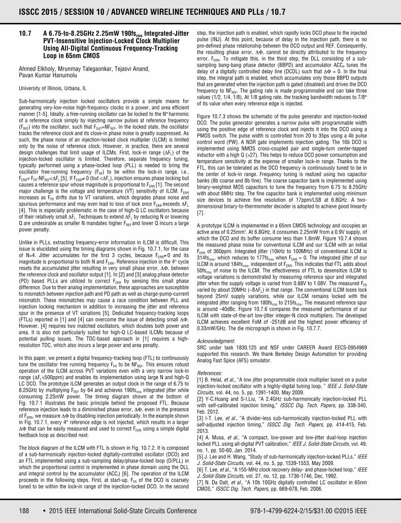
Unlike in PLLs, extracting frequency-error information in ILCM is difficult. Thisissue is elucidated using the timing diagrams shown in Fig. 10.7.1, for the caseof N=4. Jitter accumulates for the first 3 cycles, because FERR≠0 and its magnitude is proportional to both N and FERR. Reference injection in the 4th cycleresets the accumulated jitter resulting in very small phase error, ΔΦ, betweenthe reference clock and oscillator output [1]. In [2] and [3] analog phase detector(PD) based PLLs are utilized to correct FERR by sensing this small phase difference. Due to their analog implementation, these approaches are susceptibleto mismatch between injection path and PD path as well as charge-pump-currentmismatch. These mismatches may cause a race condition between PLL andinjection locking mechanism in addition to increasing the jitter and referencespur in the presence of VT variations [5]. Dedicated frequency-tracking loops(FTLs) reported in [1] and [4] can overcome the issue of detecting small ΔΦ.However, [4] requires two matched oscillators, which doubles both power andarea. It is also not particularly suited for high-Q LC-based ILCMs because ofpotential pulling issues. The TDC-based approach in [1] requires a high-resolution TDC, which also incurs a large power and area penalty.
In this paper, we present a digital frequency-tracking loop (FTL) to continuouslytune the oscillator free running frequency FFR to be NFREF. This ensures robustoperation of the ILCM across PVT variations even with a very narrow lock-inrange (ΔFL<500ppm) and enables its implementation using large N and high-QLC DCO. The prototype ILCM generates an output clock in the range of 6.75 to8.25GHz by multiplying FREF by 64 and achieves 190fsrms integrated jitter whileconsuming 2.25mW power. The timing diagram shown at the bottom ofFig. 10.7.1 illustrates the basic principle behind the proposed FTL. Because reference injection leads to a diminished phase error, ΔΦ, even in the presenceof FERR, we measure ΔΦ by disabling injection periodically. In the example shownin Fig. 10.7.1, every 4th reference edge is not injected, which results in a largerΔΦ that can be easily measured and used to correct FERR using a simple digitalfeedback loop as described next.
The block diagram of the ILCM with FTL is shown in Fig. 10.7.2. It is composedof a sub-harmonically injection-locked digitally-controlled oscillator (DCO) andan FTL implemented using a sub-sampling delay/phase-locked loop (D/PLL) inwhich the proportional control is implemented in phase domain using the DLLand integral control by the accumulator (ACCI) [6]. The operation of the ILCMproceeds in the following steps. First, at start-up, FFR of the DCO is coarselytuned to be within the lock-in range of the injection-locked DCO. In the second
step, the injection path is enabled, which rapidly locks DCO phase to the injectedpulse (INJ). At this point, because of delay in the injection path, there is no pre-defined phase relationship between the DCO output and REF. Consequently,the resulting phase error, ΔΦ, cannot be directly attributed to the frequencyerror, FERR. To mitigate this, in the third step, the DLL consisting of a sub-sampling bang-bang phase detector (BBPD) and accumulator ACCP tunes thedelay of a digitally controlled delay line (DCDL) such that ΔΦ = 0. In the finalstep, the integral path is enabled, which accumulates only those BBPD outputsthat are generated when the injection path is gated (disabled) and drives the DCOfrequency to NFREF. The gating rate is made programmable and can take threevalues (1/2, 1/4, 1/8). At 1/8 gating rate, the tracking bandwidth reduces to 7/8th
of its value when every reference edge is injected.
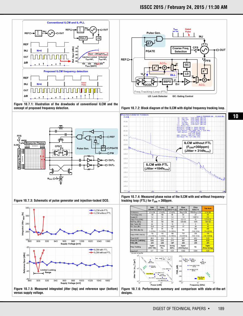
Figure 10.7.3 shows the schematic of the pulse generator and injection-lockedDCO. The pulse generator generates a narrow pulse with programmable widthusing the positive edge of reference clock and injects it into the DCO using aPMOS switch. The pulse width is controlled from 20 to 35ps using a 4b pulsecontrol word (PW). A NOR gate implements injection gating. The 16b DCO isimplemented using NMOS cross-coupled pair and single-turn center-tappedinductor with a high Q (>27). This helps to reduce DCO power consumption andtemperature sensitivity at the expense of smaller lock-in range. Thanks to theFTL, this can be tolerated as the DCO frequency is continuously tuned to be inthe center of lock-in range. Frequency tuning is realized using two capacitorbanks (8b coarse and 8b fine). The coarse capacitor bank is implemented usingbinary-weighted MOS capacitors to tune the frequency from 6.75 to 8.25GHzwith about 6MHz step. The fine capacitor bank is implemented using minimumsize devices to achieve fine resolution of 17ppm/LSB at 6.8GHz. A two-dimensional binary-to-thermometer decoder is adopted to achieve good linearity[7].
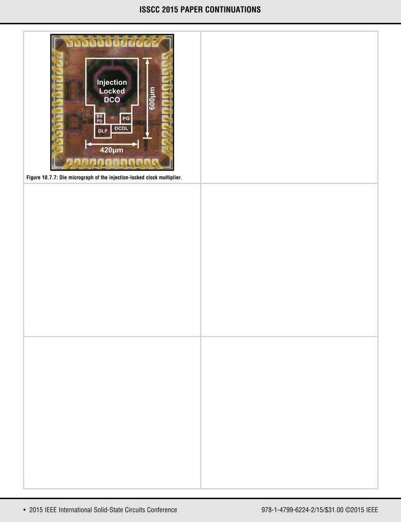
A prototype ILCM is implemented in a 65nm CMOS technology and occupies anactive area of 0.25mm2. At 6.8GHz, it consumes 2.25mW from a 0.9V supply, ofwhich the DCO and its buffer consume less than 1.8mW. Figure 10.7.4 showsthe measured phase noise for conventional ILCM and our ILCM with an initialFERR of 360ppm. Integrated jitter (10kHz to 100MHz) of conventional ILCM is314fsrms, which reduces to 177fsrms when FERR = 0. The integrated jitter of ourILCM is around 184fsrms, independent of FERR. This indicates that FTL adds about50fsrms of noise to the ILCM. The effectiveness of FTL to desensitize ILCM tovoltage variations is demonstrated by measuring reference spur and integratedjitter when the supply voltage is varied from 0.88V to 1.08V. The measured FFR
varied by about 20MHz (~8ΔFL) in that range. The conventional ILCM loses lockbeyond 25mV supply variations, while our ILCM remains locked with the integrated jitter ranging from 180fsrms to 215fsrms. The measured reference spuris around -40dBc. Figure 10.7.6 compares the measured performance of ourILCM with state-of-the-art low-jitter integer-N clock multipliers. The developedILCM achieves excellent FoM of -251dB and the highest power efficiency of0.33mW/GHz. The die micrograph is shown in Fig. 10.7.7.
Acknowledgment:SRC under task 1830.125 and NSF under CAREER Award EECS-0954969 supported this research. We thank Berkeley Design Automation for providingAnalog Fast Spice (AFS) simulator.
References:[1] B. Helal, et al., “A low jitter programmable clock multiplier based on a pulseinjection-locked oscillator with a highly-digital tuning loop, ” IEEE J. Solid-StateCircuits, vol. 44, no. 5, pp. 1391-1400, May 2009.[2] Y-C.Huang and S-I.Liu, “A 2.4GHz sub-harmonically injection-locked PLLwith self-calibrated injection timing,” ISSCC Dig. Tech. Papers, pp. 338-340,Feb. 2012.[3] I-T. Lee, et al., “A divider-less sub-harmonically injection-locked PLL withself-adjusted injection timing,” ISSCC Dig. Tech. Papers, pp. 414-415, Feb.2013.[4] A. Musa, et al., “A compact, low-power and low-jitter dual-loop injectionlocked PLL using all-digital PVT calibration,” IEEE J. Solid-State Circuits, vol. 49,no. 1, pp. 50-60, Jan. 2014.[5] J. Lee and H. Wang, “Study of sub-harmonically injection-locked PLLs,” IEEEJ. Solid-State Circuits, vol. 44, no. 5, pp. 1539-1553, May 2009.[6] T. Lee, et al., “A 155-MHz clock recovery delay- and phase-locked loop,” IEEEJ. Solid-State Circuits, vol. 27, no. 12, pp. 1736-1746, Dec. 1992.[7] N. Da Dalt, et al., “A 10b 10GHz digitally controlled LC oscillator in 65nmCMOS,” ISSCC Dig. Tech. Papers, pp. 669-678, Feb. 2006.
978-1-4799-6224-2/15/$31.00 ©2015 IEEE
189DIGEST OF TECHNICAL PAPERS •
ISSCC 2015 / February 24, 2015 / 11:30 AM
Figure 10.7.1: Illustration of the drawbacks of conventional ILCM and the concept of proposed frequency detection. Figure 10.7.2: Block diagram of the ILCM with digital frequency tracking loop.
Figure 10.7.3: Schematic of pulse generator and injection-locked DCO.
Figure 10.7.5: Measured integrated jitter (top) and reference spur (bottom)versus supply voltage.
Figure 10.7.6: Performance summary and comparison with state-of-the-artdesigns.
Figure 10.7.4: Measured phase noise of the ILCM with and without frequency-tracking loop (FTL) for FERR = 360ppm.
10
• 2015 IEEE International Solid-State Circuits Conference 978-1-4799-6224-2/15/$31.00 ©2015 IEEE
ISSCC 2015 PAPER CONTINUATIONS
Figure 10.7.7: Die micrograph of the injection-locked clock multiplier.
190 • 2015 IEEE International Solid-State Circuits Conference
ISSCC 2015 / SESSION 10 / ADVANCED WIRELINE TECHNIQUES AND PLLs / 10.8
10.8 A Wideband Fractional-N Ring PLL Using a Near-Ground Pre-Distorted Switched-Capacitor Loop Filter
Che-Fu Liang, Ping-Ying Wang
MediaTek, Hsinchu, Taiwan
Ring PLLs play an important role in mobile baseband applications. In caseswhere fine frequency resolution and low jitter are both needed, wideband fractional-N PLL architectures with quantization noise (Q-noise) cancellation arepreferred. Phase interpolators (PI) are widely used in recent literature [1-3].Although the Q-noise is reduced, decreasing supply voltages severely limit thelinearity and noise of PI. In this paper, we present a switched-capacitor loop filter(SCLF) to solve this problem. The developed SCLF with correlated double sampling (CDS) keeps the output of the charge pump (CP) near-ground toimprove its noise, linearity, and power-supply rejection ratio (PSRR).Furthermore, a calibrated 2b ADC is used to realize type-II operation.
The architecture of this PLL is shown in Fig. 10.8.1. It consists of a phase frequency detector (PFD), a CP, an SCLF, a 2b ADC, a hybrid VCO, a timing gen-erator (TGEN), a multi-modulus divider (MMD), and two digital blocks. The firstdigital block generates the MMD control signals through a MASH 1-1-1 modulator. It also generates an 8b Q-noise signal through another MASH 1-1-1modulator. This 8b signal is then segmented and scrambled into two 4b thermometer codes [2] to pre-distort the SCLF for Q-noise cancellation. A digitalcorrelator is also included to calibrate the possible gain mismatch of Q-noisecancellation. The other digital block is used to integrate the ADC output to forma digital integral control path (I-Path). A dither clocked by a 500MHz clock is alsoincluded for finer frequency resolution.
The simplified schematics and timing diagrams of the CP and SCLF are drawn inFig. 10.8.1 as well. The CP is composed of PMOS transistors only and its outputis connected to SCLF through the switch SCP, which is a pair of NMOS switchesdirecting the CP current to either SCLF or ground. The SCLF consists of threecapacitors (CUP, CDN, and CH) and three NMOS switches (SR, SDN, and SVCO). CDN
can be programmed through an 8b register and its nominal value is 4pF. CUP iscomposed of 256 unit cells (CUNIT), which are 16fF each, and every cell has twoNMOS switches (SU1 and SU2). Five clocks, ΦR, ΦU, ΦC, ΦD, and ΦS control theSCLF sequentially. This SCLF approximates a parallel RC network. The transferfunction (H(Z)) and the resistor value (RDC) are both shown in Fig. 10.8.1.
The steady-state operation of the SCLF can be divided into steps 1 to 5, whichcorrespond to ΦR, ΦU, ΦC, ΦD, and ΦS, respectively. Steps 1, 2, 4, and 5 areillustrated in Fig. 10.8.2, and step 3 is shown in Fig. 10.8.3 alone for clarity. Instep 1, both CUP and CDN are reset to 0V. Then in step 2, the CP current (ICP) isdirected to CUP through SCP and SU1 in each CUNIT for 8 periods of the hybrid VCOclock (TVCO). This creates a voltage about 250mV on CUP and all transistors of CPremain in deep saturation region with a 1V supply voltage (VDD). Compared withtraditional CPs whose outputs are usually near half the VDD, the almost-doubledvoltage headroom makes the CP noise and PSRR better. After a charge of 8ICPTVCO is stored on CUP, in step 3 we reset some of the 256 CUNIT capacitors topre-distort the CUP voltage. As illustrated in Fig. 10.8.3, all switches are openexcept for the SU2s of the N1 CUNITs. This discharges all the N1 CUNITs, and thecharge on the other N2 (256-N1) CUNITs is kept unchanged. The values of N1 andN2 are determined by the calculated Q-noise from the digital domain. For integer-N operation, N1 and N2 are both equal to 128 and after step 3 the chargeleft on CUP is always 4ICPTVCO. For fractional-N operation with a MASH 1-1-1 modulator, a time-domain Q-noise from -2TVCO to 2TVCO could be observed at thePFD inputs, which will be converted to a charge from -2ICPTVCO to 2ICPTVCO
through the CP accordingly. To cancel this charge, N1 would vary from 64 to 192depending on the Q-noise, and a charge from 2ICPTVCO to 6ICPTVCO is left on CUP
(63 to 188mV) after step 3. Please note that an offset charge of 4ICPTVCO is introduced deliberately to create a static timing offset of 4TVCO at PFD inputs,which prevents possible inter-symbol interference. This partial resetting methodmakes CUP a 7b capacitor DAC (CDAC) to replace the role of PI [1-3]. In step 4,the time-domain Q-noise from 2TVCO to 6TVCO at the PFD inputs is converted tocharge and this creates a voltage (63 to 188mV) on CDN. The integral nonlinearity(INL) of the SCLF can be simulated by combing step 3 and step 4 and it is alsoshown in Fig. 10.8.3. Referring to the TVCO domain, the maximum INL is only860fs and the distortion is dominated by the 2nd-order nonlinearity, which
introduces negligible tones with a MASH 1-1-1 modulator. Finally, assumingequal capacitance of CUP and CDN, in step 5 CUP and CDN are stacked in series tocancel the Q-noise stored on CDN in step 4 with the pre-distorted voltage on CUP
in step 3. The switch SVCO is then closed to share the charge to the hybrid VCO,and the sequence repeats from the step 1. In the steady state, the control voltage(Vctrl) would vary within ±2mV. This makes the size and resistance of the switchSVCO much smaller than the typical SCLF realizations operating near half VDD. Asmaller sharing switch also helps minimize the reference spurs. Another featureof this SCLF is that the low frequency noise of the CP can be sampled on bothCUP and CDN, and the CDS function is achieved to alleviate the design requirementof the CP.
The proposed SCLF achieves only type-I PLL operation. To add a DC pole andsave area, Vctrl is digitized through a 2b ADC and integrated in the digitaldomain. This 2b ADC is depicted in Fig. 10.8.4. A buffer is added to avoid kickback noise and three comparators (Comp1-Comp3) are used for a 4-leveloutput. Four delayed versions of ΦS (ΦS1-ΦS4) are used to make the SCLF asample and hold network for this ADC. Due to the closed-loop nature, the thresholds of the comparators (Vth1-Vth3) can be calibrated by estimating theprobability of the comparator decisions. This is achieved by monitoring thecounter values (Cnt1-Cnt3) within 10ms. This works even with the buffer gainvariation, because we look for a specific probability of each comparator decision.A comparator architecture with programmable offset [5] is used to avoid generating complicated reference voltages. Compared with the traditional 1bslicer [4], using 2b ADC makes the I-path gain larger and controllable. An additional comparator (Comp4) is added for Q-noise cancelling gain calibration.It is clocked before SVCO closes to avoid the filtering on the residual Q-noise.Good capacitor matching and the single current source in CP allow this calibration to be reserved for future use only and CDN is always set as the defaultvalue.
To work with the SCLF and the digital I-Path, the VCO is designed in a hybridway. The analog control path is realized by a set of AC-coupled varactors, andthe digital interface is implemented with a 6b resistor DAC [4]. The MMD andTGEN are designed with CMOS logic. The PFD is a traditional design [2], but onlythe down output is used by the SCLF. The PLL bandwidth is 1.5MHz.
The measured phase noise at 2GHz, reference spurs, and the in-band fractionalspurs of this PLL are all shown in Fig. 10.8.5. For the phase noise, cases usinga 1b slicer and using the 2b ADC as the I-Path quantizer are both shown. Withthe same digital gain setting, the in-band noise is improved by using the 2b ADC.Even with a higher digital gain, the in-band noise is still higher for the 1b casedue to higher Q-noise and noise folding. Due to the highly linear SCLF, the fractional spurs at FCW/218×26MHz are below -70dBc, where FCW is the frequency control word. The reference spurs are below -87dBc. Other spursindependent of FCW are also observed (from the 26MHz reference), but all ofthem are less than -68dBc. A comparison table is shown in Fig. 10.8.6. This PLLis fabricated in 40nm CMOS, and all circuits use 1V supply directly except for theVCO. The VCO VDD is regulated from a 2V supply for a better PSRR. The currentconsumption of the VCO is 2.98mA, and the current from the 1V supply is3.1mA, including the digital blocks. The total power consumption is 9.1mW. Thechip micrograph is shown in Fig. 10.8.7.
References:[1] R. K. Nandwana, et al., “A 4.25GHz-4.75GHz Calibration-Free Fractional-NRing PLL Using Hybrid Phase/Current-mode Phase Interpolator With 13.2dBPhase Noise Improvement,” IEEE Symp. VLSI Circuits, pp. 230-231, June 2014.[2] T.-K. Kao, et al., “A Wideband Fractional-N Ring PLL with Fractional-SpurSuppression Using Spectrally Shaped Segmentation,” ISSCC Dig. Tech. Papers,pp. 416-417, Feb. 2013.[3] D.-W. Jee, et al., “A 0.1-fref BW 1GHz Fractional-N PLL with FIR-EmbeddedPhase-Interpolator-Based Noise Filtering,” ISSCC Dig. Tech. Papers, pp. 94-95,Feb. 2011.[4] Y.-C. Huang, et al., “A 2.4GHz ADPLL with Digital-Regulated Supply-Noise-Insensitive and Temperature-Self-Compensated Ring DCO,” ISSCC Dig. Tech.Papers, pp. 270-271, Feb. 2014.[5] Y.-S. Shu, “A 6b 3GS/s 11mW Fully Dynamic Flash ADC in 40nm CMOS withReduced Number of Comparators,” IEEE Symp. VLSI Circuits, pp. 26-27, June2012.
978-1-4799-6224-2/15/$31.00 ©2015 IEEE
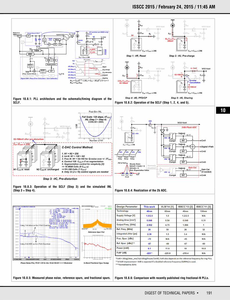
191DIGEST OF TECHNICAL PAPERS •
ISSCC 2015 / February 24, 2015 / 11:45 AM
Figure 10.8.1: PLL architecture and the schematic/timing diagram of theSCLF. Figure 10.8.2: Operation of the SCLF (Step 1, 2, 4, and 5).
Figure 10.8.3: Operation of the SCLF (Step 3) and the simulated INL(Step 3 + Step 4).
Figure 10.8.5: Measured phase noise, reference spurs, and fractional spurs. Figure 10.8.6: Comparison with recently published ring fractional-N PLLs.
Figure 10.8.4: Realization of the 2b ADC.
10

• 2015 IEEE International Solid-State Circuits Conference 978-1-4799-6224-2/15/$31.00 ©2015 IEEE
ISSCC 2015 PAPER CONTINUATIONS
Figure 10.8.7: Chip micrograph.

192 • 2015 IEEE International Solid-State Circuits Conference
ISSCC 2015 / SESSION 10 / ADVANCED WIRELINE TECHNIQUES AND PLLs / 10.9
10.9 A 13.1-to-28GHz Fractional-N PLL in 32nm SOI CMOS with a ΔΣ Noise-Cancellation Scheme
Mark Ferriss, Bodhisatwa Sadhu, Alexander Rylyakov, Herschel Ainspan, Daniel Friedman
IBM Research, Yorktown Heights, NY
A key challenge in high-performance I/O, as well as in reconfigurable radio andradar applications, is the generation of a clean clock signal supporting a widerange of frequencies. The introduction of fractional-N synthesis capability forwide-tuning-range applications enables generation of arbitrary output frequencies within that range from a single choice of reference frequency. A critical challenge in fractional-N synthesizer design is the cancellation of thedeterministic component of the fractional-N ΔΣ noise, allowing fractional-Nsolutions to be applied even in noise-sensitive contexts. In this work, we presenta flexible, wide tuning range, fractional-N PLL implemented in 32nm SOI CMOStechnology, introducing two separate methods—one in the proportional pathand one in the integral path—to process and suppress ΔΣ noise. The demonstrated design includes an integrated automatic calibration loop to optimize noise suppression, uses a dual VCO complex to support generation ofany output frequency from 13 to 28GHz from a reference clock in the range of15 to 300 MHz, and also supports extended tuning down to 1GHz through theuse of configurable output dividers.
The architecture of the implemented PLL, shown in Fig. 10.9.1, extends the integer-N hybrid analog/digital approach presented in [1]. In baseline PLL operation, the feedback and reference clocks are compared in the PFD block,which provides both a 1b bang-bang signal to the digital integral path and a linear phase error signal to the analog proportional path. The bang-bang signalis processed in the integral path to create a control word that is applied to theVCO complex; the linear phase-error signal is passed through a simplified chargepump and a loop filter as in [1] and is then applied to the VCO complex. Only oneof the two VCOs is activated at any given time. The full-rate output is divided bythe configurable static prescaler and then the multi-modulus divider to create thefeedback clock.
The proportional-path cancellation approach flows from the observations that(1) a significant portion of the instantaneous phase error at the input of the PFDis deterministic, arising from the ΔΣ operation, and (2) the digital state machinewithin the PLL includes the data needed to predict the expected value of thaterror. Cancelling deterministic ΔΣ noise can therefore be achieved by applyingcompensating delays to the linear phase detector output signals before applyingthe generated UP/DOWN pulses to the proportional-path charge pump. By cancelling the ΔΣ noise in the time domain cancellation can be implemented withexclusively digital building blocks, even in the context of an analog control path;note that this approach does not require any quantization of the VCO/referenceclock induced phase error. Furthermore, the cancellation takes place before thelow-pass filter of the proportional path, such that the non-idealities of the delaypath can be shaped to high frequencies using standard DAC techniques andremoved from the loop before being applied to the VCO controls.
In the implementation of this approach (Fig. 10.9.2), a calibrated digital-to-timeconverter composed of the delay controller and delay (ΔT) blocks is placedbetween the PFD sampling latches and proportional-path outputs. A digital statemachine calculates the magnitude of the instantaneous phase error caused bythe fractional-N divider by integrating the difference between the input and output of the divider ΔΣ, similar to [2] and [3]. This result is scaled and appliedto the PFD programmable ΔT elements. For each comparison the PFD makes,the noise from the ΔΣ will introduce error, adding a deterministic component tothe pulse widths of one of the two phase-detector sampling flip-flops (UP_A orDWN_A in Fig. 10.9.2). For each phase comparison, a set of multiplexers routesUP_A and DWN_A such that the signal, which includes the deterministic errorpasses through the compensating ΔT, while the other signal passes through adummy cell which mimics the zero delay settings of the programmable path. Inthis way, the effects of the deterministic noise added by the ΔΣ are removed inthe time domain from the outputs of the phase detector (UP and DWN) beforethey are applied to the low-pass proportional-path filter. By using only one delayelement and a set of multiplexers, the implementation of the cancellation pathcontrol scheme is orthogonal to PLL operation, as changes in cancellation-pathgain only affect phase noise outside the PLL bandwidth.
Successful operation of the proportional-path cancellation approach requiresthat the digital representation of the delay be calibrated to the actual differentialdelay created by the delay elements. To this end, the PLL includes an integratedautomatic compensation loop, driven by a monitoring BB-PD placed at the output of the delay elements. Errors in cancellation path gain are detected bycorrelating the sign of the time delay with the early/late output of the monitor BB-PD, then adjusting the gain to drive the correlation to zero. The highly digitaldelay circuit, illustrated in Fig. 10.9.3, is implemented using logic elements froma standard-cell library; the delay-circuit control scheme includes an additionalΔΣ to shape delay quantization error to high frequencies; delay output is appliedto the VCO through the low-pass proportional-path loop filter.
The digital integral path, which derives phase-error information from a singleBB-PFD, operates in parallel with the proportional path. In fractional-N mode, thedeterministic error added by the divider ΔΣ is usually much larger than the PLLintrinsic phase error in the locked state, so much of the early/late output fromthe BB-PFD reflects only deterministic noise. Rather than introducing a TDC toaddress this issue, the integral path in the design (predictor block of Fig. 10.9.1)uses post-processing of the BB-PFD outputs. The integral path predictor statemachine first calculates the magnitude of the phase error caused by the ΔΣmodulator at the BB-PFD input, then predicts the expected output of the BB-PFDsolely on this basis. For each BB-PFD phase comparison, a correct predictionimplies that no meaningful phase error has been detected, so a digital 0 outputis provided, leaving VCO controls unchanged. If the prediction is incorrect, itimplies (1) that phase correction is required, and (2) that the lower bound of theerror magnitude is at least that of the predicted phase, so a digital output valueequal to the predicted phase error magnitude is provided. Predictor output issent to a digital accumulator and ultimately yields the integral path VCO controlsignals. Each VCO is a 16-band cross-coupled LC-VCO with digital/analog frequency controls for use with the integral/proportional paths.
The PLL is implemented in 32nm SOI CMOS, occupies an active area of400×600μm2, and is measured using wafer probing. The dual-VCO PLL locksover a range of 13.1 to 28GHz (13.1 to 21GHz and 18.5 to 28GHz for the lowerand upper VCOs, respectively), nominally drawing 31mA from 1.0V.Figure 10.9.4 shows the PLL measured phase noise operating at 22.25GHz (1)in integer-N mode and (2) in fractional-N mode with and without noise cancellation enabled; with cancellation on, fractional-N mode performanceapproaches that of integer-N mode. As shown in the figure, in fractional-N mode(104MHz reference, 22.25GHz output), activating noise cancellation improvesphase noise at a 10MHz offset from -106.1dBc/Hz to -116.8dBc/Hz. To illustratethe performance of the automatic gain calibration infrastructure, Fig. 10.9.5shows measured integrated noise under three scenarios: (1) cancellation andauto gain selection active (lower horizontal line, left); (2) cancellation off (upperhorizontal line); and (3) as gain settings are manually swept through the controlrange (central curve). The automatically calibrated gain setting corresponds tothe lowest integrated jitter achieved by manual stepping, confirming successfuloperation the auto gain infrastructure. To evaluate the integral path enhancement, frequency acquisition experiments with the integral path predictoractive and while varying integral path gain are undertaken, with strong dependency of lock time on integral path gain observed as expected.Figure 10.9.6 shows the measured tuning range of the dual VCO complex with arepresentative fractional-N 28GHz spectrum. Figure 10.9.7 shows a micrographwith layout annotation of the prototype PLL.
Acknowledgments:This work has been partially funded by DARPA under contract # HR0011-12-C-0087. The views, opinions, and/or findings contained in this presentation arethose of the author/presenter and should not be interpreted as representing theofficial views or policies, either expressed or implied, of DARPA or the DoD.
References:[1] M. Ferriss et al., “A 28GHz Hybrid PLL in 32nm SOI CMOS,” J. Solid-StateCircuits, vol. 49, pp. 1027-1035 Dec. 2014.[2] D. Tasca, et al, “A 2.9–4.0-GHz Fractional-N Digital PLL With Bang-BangPhase Detector and 560- Integrated Jitter at 4.5-mW Power,” J. Solid-StateCircuits, vol. 46, pp. 2745-2758 Dec. 2011.[3] A. Swaminathan, et al, “A Wide-Bandwidth 2.4 GHz ISM Band Fractional-NPLL with Adaptive Phase Noise Cancellation,” J. Solid-State Circuits, vol. 42,pp. 2639-2650, Dec. 2007.
978-1-4799-6224-2/15/$31.00 ©2015 IEEE
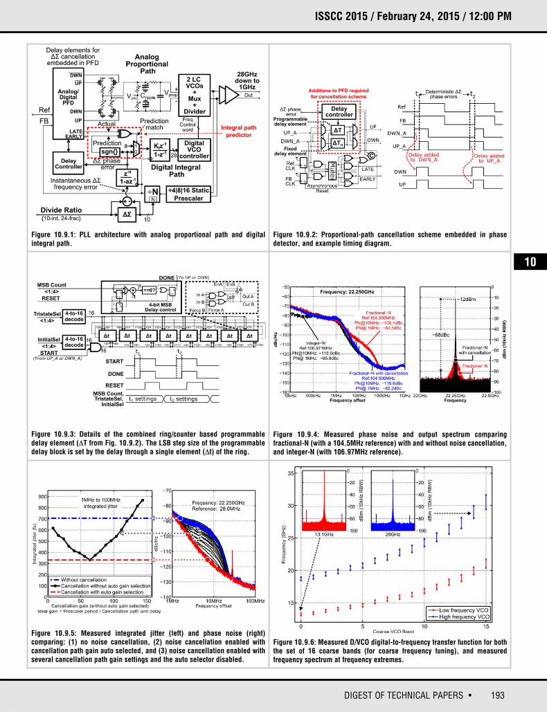
193DIGEST OF TECHNICAL PAPERS •
ISSCC 2015 / February 24, 2015 / 12:00 PM
Figure 10.9.1: PLL architecture with analog proportional path and digital integral path.
Figure 10.9.2: Proportional-path cancellation scheme embedded in phasedetector, and example timing diagram.
Figure 10.9.3: Details of the combined ring/counter based programmabledelay element (ΔT from Fig. 10.9.2). The LSB step size of the programmabledelay block is set by the delay through a single element (Δt) of the ring.
Figure 10.9.5: Measured integrated jitter (left) and phase noise (right) comparing: (1) no noise cancellation, (2) noise cancellation enabled with cancellation path gain auto selected, and (3) noise cancellation enabled withseveral cancellation path gain settings and the auto selector disabled.
Figure 10.9.6: Measured D/VCO digital-to-frequency transfer function for boththe set of 16 coarse bands (for coarse frequency tuning), and measured frequency spectrum at frequency extremes.
Figure 10.9.4: Measured phase noise and output spectrum comparing fractional-N (with a 104.5MHz reference) with and without noise cancellation,and integer-N (with 106.97MHz reference).
10
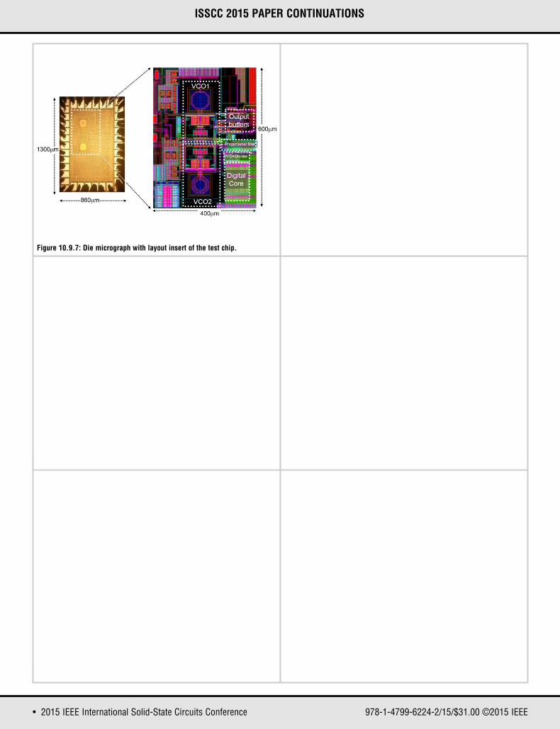
• 2015 IEEE International Solid-State Circuits Conference 978-1-4799-6224-2/15/$31.00 ©2015 IEEE
ISSCC 2015 PAPER CONTINUATIONS
Figure 10.9.7: Die micrograph with layout insert of the test chip.