Scanned by CamScanner - VSM
53
Scanned by CamScanner
-
Upload
khangminh22 -
Category
Documents
-
view
0 -
download
0
Transcript of Scanned by CamScanner - VSM

Scanned by CamScanner

Scanned by CamScanner

Scanned by CamScanner

Scanned by CamScanner

Scanned by CamScanner

Scanned by CamScanner

Scanned by CamScanner
Scanned by CamScanner

Scanned by CamScanner

Scanned by CamScanner

Scanned by CamScanner

Scanned by CamScanner

Scanned by CamScanner

Scanned by CamScanner

Scanned by CamScanner

Scanned by CamScanner
Scanned by CamScanner

Scanned by CamScanner
Scanned by CamScanner

Scanned by CamScanner

Scanned by CamScanner

Scanned by CamScanner

Scanned by CamScanner

Scanned by CamScanner

Scanned by CamScanner

Scanned by CamScanner

Scanned by CamScanner

Scanned by CamScanner

Scanned by CamScanner

Scanned by CamScanner

Scanned by CamScanner

Scanned by CamScanner

Scanned by CamScanner
Scanned by CamScanner

Scanned by CamScanner

Scanned by CamScanner

Scanned by CamScanner

Scanned by CamScanner
Scanned by CamScanner

UNIT-III
Introduction to Uni-Junction Transistor
Uni-junction transistor
Uni-junction transistor is also known as double-base diode because it is a 2-layered, 3-terminal
solid-state switching device. It has only one junction so it is called as a uni-junction device. The
unique characteristic feature of this device is such that when it is triggered, the emitter current
increases until it is restricted by an emitter power supply. Owing to its low cost, it can be used in
a wide range of applications including oscillators, pulse generators and trigger circuits, etc. It is
a low-power absorbing device and can be operated under normal conditions.
Construction of UJT
UJT is a three-terminal, single-junction, two-layered device, and it is similar to a thyristor
compare to a transistors. It has a high-impedance off state and low-impedance on state quite
similar to a thyristor. From off state to an on state, switching is caused by conductivity
modulation and not by a bipolar transistor action.
Construction of UJT
The silicon bar has two Ohmic contacts designated as base1 and base2, as shown in the fig.
The function of the base and the emitter are different from the base and emitter of a bipolar
transistor.
The emitter is of P-type, and it is heavily doped. The resistance between B1 and B2 when the
emitter is open-circuited is called an inter-base resistance. The emitter junction is usually
situated closer to the base B2 than the base B1. So the device is not symmetrical, because
symmetrical unit does not provide electrical characteristics to most of the applications.

The symbol for uni-junction transistor is shown in the fig. When the device is forward-biased, it
is active or is in the conducting state. The emitter is drawn at an angle to the vertical line which
represents the N-type material slab and the arrow head points in the direction of conventional
current.
Operation of a UJT
This transistor operation starts by making the emitter supply voltage to zero, and its emitter diode
is reverse biased with the intrinsic stand-off voltage. If VB is the voltage of the emitter diode,
then the total reverse bias voltage is VA + VB = Ƞ VBB + VB. For silicon VB = 0.7 V, If VE gets
slowly increases to the point where VE = Ƞ VBB, then IE will be reduced to zero. Therefore, on
each side of the diode, equal voltages results no current flow through it, neither in reverse bias
nor in forward bias.
When the emitter supply voltage is increased rapidly, then the diode becomes forward-biased
and exceeds the total reverse bias voltage (Ƞ VBB + VB). This emitter voltage value VE is
called the peak-point voltage and is denoted by VP. When VE = VP, emitter current IE flows
through the RB1 to the ground, that is, B1. This is the minimum current required for triggering
the UJT. This is called the peak-point emitter current and is denoted by IP. Ip is inversely
proportional to the Inter-base voltage, VBB.
Now when the emitter diode starts conducting, charge carriers are injected into the RB region of
the bar. As the resistance of a semiconductor material depends upon doping, the resistance of
RB decreases due to additional charge carriers.
Then the voltage drop across RB also decreases, with the decrease in resistance because the
emitter diode is heavily forward biased. This in turn results in larger forward current, and as a
result charge carriers are injected and it will cause the reduction in the resistance of the RB
region. Thus, the emitter current goes on increasing until the emitter power supply is in limited
range.
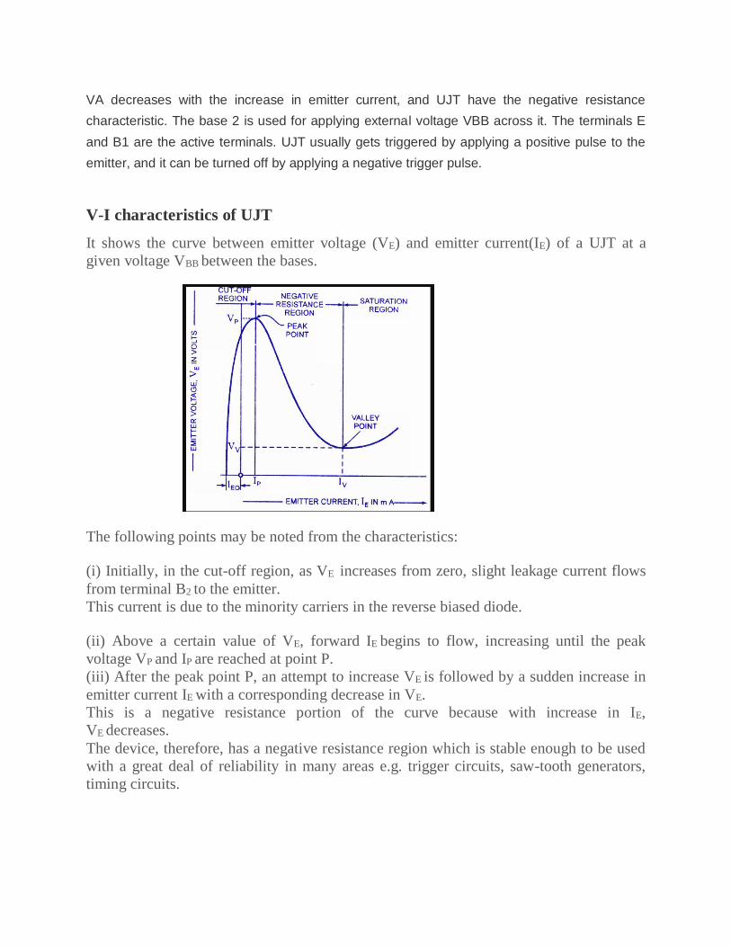
VA decreases with the increase in emitter current, and UJT have the negative resistance
characteristic. The base 2 is used for applying external voltage VBB across it. The terminals E
and B1 are the active terminals. UJT usually gets triggered by applying a positive pulse to the
emitter, and it can be turned off by applying a negative trigger pulse.
V-I characteristics of UJT
It shows the curve between emitter voltage (VE) and emitter current(IE) of a UJT at a
given voltage VBB between the bases.
The following points may be noted from the characteristics:
(i) Initially, in the cut-off region, as VE increases from zero, slight leakage current flows
from terminal B2 to the emitter.
This current is due to the minority carriers in the reverse biased diode.
(ii) Above a certain value of VE, forward IE begins to flow, increasing until the peak
voltage VP and IP are reached at point P.
(iii) After the peak point P, an attempt to increase VE is followed by a sudden increase in
emitter current IE with a corresponding decrease in VE.
This is a negative resistance portion of the curve because with increase in IE,
VE decreases.
The device, therefore, has a negative resistance region which is stable enough to be used
with a great deal of reliability in many areas e.g. trigger circuits, saw-tooth generators,
timing circuits.

iv) The negative portion of the curve lasts until the valley point V is reached with valley-
point voltage VV and valley-point current IV. After the valley point, the device is driven to
saturation.
Fig.2 shows the typical family of VE /IE characteristics of a UJT at different voltages
between the bases.
It is clear that peak-point voltage (=ηVBB+VD) falls steadily with reducing VBB and so
does the valley-point voltage Vv.
Advantages of UJT
The UJT has achieved great popularity due to the following reasons:
1. It is low cost device.
2. It has excellent characteristics.
3. It is a low-power absorbing device under normal operating conditions.
Applications
Due to the above reasons, this device is being used in a variety of applications. A few
include oscillators, trigger circuits, saw-tooth generators, bistable network etc.
What is a Light Emitting Diode?
The lighting emitting diode is a p-n junction diode. It is a specially doped diode and made up of a
special type of semiconductors. When the light emits in the forward biased, then it is called as a
light emitting diode.
How does the Light Emitting Diode work?
The light emitting diode simply, we know as a diode. When the diode is forward biased, then the
electrons & holes are moving fast across the junction and they are combining constantly,
removing one another out. Soon after the electrons are moving from the n-type to the p-type
silicon, it combines with the holes, then it disappears. Hence it makes the complete atom &
more stable and it gives the little burst of energy in the form of a tiny packet or photon of light.

The above diagram shows how the light emitting diode works and the step by step process of
the diagram.
From the diagram, we can observe that the N-type silicon is in red color and it contains the
electrons, they are indicated by the black circles.
The P- type silicon is in the blue color and it contains holes, they are indicated by the white
circles.
The power supply across the p-n junction makes the diode forward biased and pushing the
electrons from n-type to p-type. Pushing the holes in the opposite direction.
Electron and holes at the junction are combined.
The photons are given off as the electrons and holes are recombined.
Working Principle of LED
The working principle of the Light emitting diode is based on the quantum theory. The quantum
theory says that when the electron comes down from the higher energy level to the lower
energy level then, the energy emits from the photon. The photon energy is equal to the energy
gap between these two energy levels. If the PN-junction diode is in the forward biased, then the
current flows through the diode.

Working Principle of LED
The flow of current in the semiconductors is caused by the both flow of holes in the opposite
direction of current and flow of electrons in the direction of the current. Hence there will be
recombination due to the flow of these charge carriers.
The recombination indicates that the electrons in the conduction band jump down to the valence
band. When the electrons jump from one band to another band the electrons will emit the
electromagnetic energy in the form of photons and the photon energy is equal to the forbidden
energy gap.
I-V Characteristics of LED
There are different types of light emitting diodes are available in the market and there are
different LED characteristics which include the color light, or wavelength radiation, light intensity.
The important characteristic of the LED is color. In the starting use of LED, there is the only red
color. As the use of LED is increased with the help of the semiconductor process and doing the
research on the new metals for LED, the different colors were formed.

I-V Characteristics of LED
The following graph shows the approximate curves between the forward voltage and the
current. Each curve in the graph indicates the different color
Applications of Light Emitting Diodes
There are many applications of the LED and some of them are explained below.
LED is used as a bulb in the homes and industries
The light emitting diodes are used in the motorcycles and cars
These are used in the mobile phones to display the message At the traffic light signals led’s are used
Advantages of LED’s
The cost of LED’s is less and they are tiny.
By using the LED’s the electricity is controlled. The intensity of the LED differs with the help of the microcontroller.
What is a LCD(Liquid Crystal Display)?
A liquid crystal display or LCD draws its definition from its name itself. It is combination of two
states of matter, the solid and the liquid. LCD uses a liquid crystal to produce a visible image.
Liquid crystal displays are super-thin technology display screen that are generally used in laptop
computer screen, TVs, cell phones and portable video games. LCD’s technologies allow
displays to be much thinner when compared to cathode ray tube (CRT) technology.
Liquid crystal display is composed of several layers which include two polarized panel filters and electrodes. LCD technology is used for displaying the image in notebook or some other electronic devices like mini computers. Light is projected from a lens on a layer of liquid crystal. This combination of colored light with the grayscale image of the crystal (formed as electric current flows through the crystal) forms the colored image. This image is then displayed on the screen.

Silicon Controlled
Rectifier
Silicon controlled rectifier is also a unidirectional device as it conducts only in one direction. By
triggering appropriately, the thyristor can be used as an open circuit switch and also as a
rectifying diode. However, thyristor can not be used as an amplifier and it can be used only for
switching operation controlled with triggering pulse of gate terminal.
Thyristor can be manufactured using a variety of materials such as silicon, silicon carbide,
gallium arsenide, gallium nitride, and so on. But, the good thermal conductivity, high current
capability, high voltage capability, economical processing of silicon has made it to prefer
compared to other materials for making thyristors, hence, they are also called as silicon
controlled rectifiers.
Silicon Controlled Rectifier Working
The thyristor working can be understood by considering the three states modes of operation of
silicon controlled rectifier. The three modes of operation of thyristor are as follows:
Reverse blocking mode
Forward blocking mode
Forward conducting mode
Reverse Blocking Mode
If we reverse the anode and cathode connections of the thyristors, then the lower and upper diodes are reverse
biased. Thus, there is no conduction path, so no current will flow. Hence, is called as reverse blocking mode.
Forward Blocking Mode
In general, without any triggering pulse to gate terminal, from anode to cathode). This is
because, we connected two diodes (both upper and lower diodes are forward biased) together to
form a thyristor. But, the junction between these two diodes is reverse biased, which eliminates
the flow of current from top to bottom. Hence, this state is termed as forward blocking mode. In

this mode, even though thyristor is having condition like a conventional forward biased diode, it
will not conduct as the gate terminal is not triggered. Forward Conducting Mode
In this forward conducting mode, the anode voltage must be greater than the cathode voltage and
the third terminal gate must be triggered appropriately for the conduction of the thyristor. This is
because, whenever the gate terminal is triggered, then the lower transistor will conduct which
switches on the upper transistor and then the upper transistor switches on the lower transistor and
thus the transistors activates each other. This process of internal positive feedback of both the
transistors repeats until both gets fully activated and then the current will from anode to cathode.
So, this mode of operation of silicon controlled rectifier is called as forward conduction mode.
Silicon Controlled Rectifier Characteristics
The figure shows the silicon controlled rectifier characteristics and also represents the thyristor
operation in three different modes such as reverse blocking mode, forward blocking mode, and
forward conducting mode. The V-I characteristics of thyristor also represent the reverse blocking
voltage, forward blocking voltage, reverse breakdown voltage, holding current, break-over
voltage, and so on as shown in the figure.
Silicon Controlled Rectifier Applications
Applications. SCRs are mainly used in devices where the control of high power, possibly
coupled with high voltage, is demanded. Their operation makes them suitable for use in medium-
to high-voltage AC power control applications, such as lamp dimming, power regulators and
motor control.

How LCDs are Constructed?
LCD Layered Diagram
Simple facts that should be considered while making an LCD:
1. The basic structure of LCD should be controlled by changing the applied current.
2. We must use a polarized light.
3. Liquid crystal should able be to control both of the operation to transmit or can also able to change the polarized light.
How LCDs Work?
The principle behind the LCD’s is that when an electrical current is applied to the liquid crystal
molecule, the molecule tends to untwist. This causes the angle of light which is passing through
the molecule of the polarized glass and also cause a change in the angle of the top polarizing
filter. As a result a little light is allowed to pass the polarized glass through a particular area of
the LCD. Thus that particular area will become dark compared to other. The LCD works on the
principle of blocking light. While constructing the LCD’s, a reflected mirror is arranged at the
back. An electrode plane is made of indium-tin oxide which is kept on top and a polarized glass
with a polarizing film is also added on the bottom of the device. The complete region of the LCD
has to be enclosed by a common electrode and above it should be the liquid crystal matter.
Next comes to the second piece of glass with an electrode in the form of the rectangle on the
bottom and, on top, another polarizing film. It must be considered that both the pieces are kept at
right angles. When there is no current, the light passes through the front of the LCD it will be
reflected by the mirror and bounced back. As the electrode is connected to a battery the current
from it will cause the liquid crystals between the common-plane electrode and the electrode

shaped like a rectangle to untwist. Thus the light is blocked from passing through. That particular
rectangular area appears blank.
Advantages of an LCD’s: LCD’s consumes less amount of power compared to CRT and LED
LCD’s are consist of some microwatts for display in comparison to some mill watts for LED’s
LCDs are of low cost
Provides excellent contrast
LCD’s are thinner and lighter when compared to cathode ray tube and LED
Disadvantages of an LCD’s: Require additional light sources
Range of temperature is limited for operation
Low reliability
Speed is very low
LCD’s need an AC drive
Applications of Liquid Crystal Display
Liquid crystal thermometer
Optical imaging
The liquid crystal display technique is also applicable in visualization of the radio frequency
waves in the waveguide
SILICON CONTROLLED RECTIFIER silicon controlled rectifier remains switched off, indicating no current flow in the forward
direction (Silicon Controlled Rectifier
Thyristor or silicon controlled rectifier is a multilayer semiconductor device and is similar to the
transistor. Silicon controlled rectifier consists of three terminals (anode, cathode, and gate)
unlike the two terminal diode (anode and cathode) rectifier. The diodes are termed as
uncontrolled rectifiers as they conduct (during forward bias condition without any control)
whenever the anode voltage of the diode is greater than cathode voltage.
Diode and Thyristor
But, the silicon controlled rectifiers doesn’t conduct even though the anode voltage is greater
than the cathode voltage unless until the (third terminal) gate terminal is triggered. Thus, by
providing the triggering pulse to the gate terminal, we can control the operation (ON or OFF) of
thyristor. Hence, the thyristor is also called as controlled rectifier or silicon controlled rectifier.

Silicon Controlled Rectifier Basics
Unlike two layers (P-N) in the diode and three layers (P-N-P or N-P-N) in transistors,
the silicon controlled rectifier consists of four layers (P-N-P-N) with three P-N junctions that are
connected in series. The silicon controlled rectifier or thyristor is represented by the symbol as
shown in the figure.
What is a Varactor Diode?
Varactor diode is a one kind of semiconductor microwave solid-state device and the
applications of this diode mainly involve in where variable capacitance is preferred which can be
accomplished by controlling voltage. These diodes are also named as varicap diodes. Even
though the outcome of the variable capacitance can be showed by the normal P-N junction
diodes, but these diodes are chosen for giving the desired capacitance changes as they are
special types of diodes. Varactor diodes are specifically fabricated and optimized such that they
permits a high range of changes in capacitance.
The different types of Varactor diodes are available in the market such as hyperabrupt,
abrupt and gallium-arsenide Varactor diodes. The symbol of the Varactor diode is shown in the
above figure that includes a capacitor symbol at one end of the diode that signifies the
characteristics of the variable capacitor of the Varactor diodes.
The symbol of the Varactor diode looks like a common PN- junction diode that includes
two terminals namely the cathode and the anode. And at one end this diode is inbuilt with two
lines that specifies the capacitor symbol.
Working of a Varactor Diode
To know the Varactor diode working principle, we must know the function of
capacitor and capacitance. Let us consider the capacitor that comprises of two plates alienated by
an insulator as shown in the figure.

We know that, the capacitance of a capacitor is directly proportional to the region of the
terminals, as the region of the terminals increases the capacitance of the capacitor increases. When the
diode is in the reverse biased mode, where the two regions of P-type and N-type are able to conduct and
thus can be treated as two terminals. The depletion area between the P-type & N-type regions can be
considered as insulating dielectric. Therefore, it is similar to the capacitor shown above.
The volume of the depletion region of the diode varies with change in reverse bias. If the
reverse voltage of the diode is increased, then the size of the depletion region increases.
Likewise, if the reverse voltage of the Varactor diode is decreased, then the size of the depletion
region decreases. Hence, by changing the reverse bias of the diode the capacitance can be
changed.
Characteristics of Varactor Diode
The characteristics of Varactor diode have the following:
These diodes significantly generate less noise compared to other diodes.
The cost of these diodes is available at lower and more reliable also.
These diodes are very small in size and very light weight. There is no useful when it is operated in forward bias.
In reverse bias mode, Varactor diode enhances the capacitance as shown in the graph below.
Applications of Varactor Diode

The applications of Varactor Diode mainly involve within the RF design arena However, in this
article, we are discussing about the couple of applications of Varactor diodes, to illustrate how
these diodes can be used in a practical. The capacitor in a practical circuit can be changed with
the Varactor diode, but it is necessary to make sure the tune voltage that is, the voltage
necessary to set the diode capacitance. And to ensure that this diode is not influenced by the
bias voltage in the circuit. By using voltage control technique in the diode circuit, changing
capacitance can be offered.