Samsung SGH-E750 service manual
56
GSM TELEPHONE SGH-E750 GSM TELEPHONE CONTENTS 1. Specification 2. Circuit Description 3. Exploded Views and Parts List 4. Electrical Parts List 5. Block Diagrams 6. PCB Diagrams 7. Flow Chart of Troubleshooting
-
Upload
khangminh22 -
Category
Documents
-
view
9 -
download
0
Transcript of Samsung SGH-E750 service manual

GSM TELEPHONE
SGH-E750
GSM TELEPHONE CONTENTS
1. Specification
2. Circuit Description
3. Exploded Views and Parts List
4. Electrical Parts List
5. Block Diagrams
6. PCB Diagrams
7. Flow Chart of Troubleshooting

Samsung Electronics Co.,Ltd. September. 2005
Printed in Korea.
Code No.: GH68-08355A
BASIC.
This Service Manual is a property of Samsung Electronics Co.,Ltd.Any unauthorized use of Manual can be punished under applicableInternational and/or domestic law.
ⓒ

SAMSUNG Proprietary-Contents may change without notice
1. Specification
This Document can not be used without Samsung's authorization
1-1
GSM900Phase 1
EGSM 900Phase 2
DCS1800Phase 1 PCS1900
Freq. Band[MHz]Uplink/Downlink
890~915935~960
880~915925~960
1710~17851805~1880
1850~19101930~1990
ARFCN range 1~124 0~124 &975~1023 512~885 512~810
Tx/Rx spacing 45MHz 45MHz 95MHz 80MHz
Mod. Bit rate/ Bi t Per iod
270.833kbps3.692us
270.833kbps3.692us
270.833kbps3.692us
270.833kbps3.692us
Time Slot Per iod/ Frame Period
576.9us4.615ms
576.9us4.615ms
576.9us4.615ms
576.9us4.615ms
Modulat ion 0.3GMSK 0.3GMSK 0.3GMSK 0.3GMSK
MS Power 33dBm~13dBm 33dBm~5dBm 30dBm~0dBm 30dBm~0dBm
Power Class 5pcl ~ 15pcl 5pcl ~ 19pcl 0pcl ~ 15pcl 0pcl ~ 15pcl
Sensi t ivi ty -102dBm -102dBm -100dBm -100dBm
TDMA Mux 8 8 8 8
Cel l Radius 35Km 35Km 2Km -
1-1. GSM General Specification

SAMSUNG Proprietary-Contents may change without notice
Specification
This Document can not be used without Samsung's authorization
1-2
TX Powercontrol level
GSM900
5 33±3 dBm
6 31±3 dBm
7 29±3 dBm
8 27±3 dBm
9 25±3 dBm
10 23±3 dBm
11 21±3 dBm
12 19±3 dBm
13 17±3 dBm
14 15±3 dBm
15 13±3 dBm
16 11±5 dBm
17 9±5 dBm
18 7±5 dBm
19 5±5 dBm
TX Powercontrol level
DCS1800
0 30±3 dBm
1 28±3 dBm
2 26±3 dBm
3 24±3 dBm
4 22±3 dBm
5 20±3 dBm
6 18±3 dBm
7 16±3 dBm
8 14±3 dBm
9 12±4 dBm
10 10±4 dBm
11 8±4dBm
12 6±4 dBm
13 4±4 dBm
14 2±5 dBm
15 0±5 dBm
1-2. GSM TX power class
TX Powercontrol level
PCS1900
0 30±3 dBm
1 28±3 dBm
2 26±3 dBm
3 24±3 dBm
4 22±3 dBm
5 20±3 dBm
6 18±3 dBm
7 16±3 dBm
8 14±3 dBm
9 12±4 dBm
10 10±4 dBm
11 8±4dBm
12 6±4 dBm
13 4±4 dBm
14 2±5 dBm
15 0±5 dBm

SAMSUNG Proprietary-Contents may change without notice
2. Circuit Description
2-1
This Document can not be used without Samsung's authorization
2-1. SGH-E750 RF Circuit Description
2-1-1. RX PART
- FEM(MODULE100) → Switching Tx, Rx path for GSM900, DCS1800 and PCS1900 by logic controlling.
- FEM Control Logic (MODULE100) → Truth Table
VC1 VC2 VC3
Tx Mode (GSM900) H L L
Tx Mode (DCS1800/1900) L H L(H)
Rx Mode (GSM900) L L L
Rx Mode (DCS1800) L L L
Rx Mode (PCS1900) L L H
- VC-TCXO-2146C6(26MHz) (OSC100)
This module generates the 26MHz reference clock to drive the logic and RF.
It is turned on when the supply voltage is applied.
After buffering a reference clock of 26MHz is supplied to the other parts of the system through the transceiver pin
VCXOOUT1.
- Transceiver (U100)
This chip is a RF transceiver IC for GSM850/900, DCS1800, and PCS1900 Quad band cellular system, and incorporates
GPRS transceiver capability, and integrates most of the low power silicon functions of a transceiver.
It incorporates triple RF LNAs, direct conversion mixers which are IQ demodulator, an auto offset calibrated
programmable gain amplifier with baseband filter for IQ chains, RF synthesizer, a I/Q modulator, offset PLL, IF
synthesizer, and the circuits which are needed polar loop architecture for the transmitter.
2-1-2. TX PARTTransmitter of the transceiver is capable of GMSK and 8-PSK modulation, providing support for conventional GSM and
GPRS. The modulated signal out of the transceiver is fed into Power Amplifer Module(U101). PAM output signal is
radiated to the air through FEM(MODULE1) and antenna.

SAMSUNG Proprietary-Contents may change without notice
Circuit Description
2-2
This Document can not be used without Samsung's authorization
2-2. Baseband Circuit description of SGH-E750
2-2-1. PCF50603 (U405)
- Power Management
Eight low-dropout regulators designed specifically for GSM applications power the terminal and help ensure optimal
system performance and long battery life. A programmable boost converter provides support for 1.8V, 3.0V SIMs,
while a self-resetting, electronically fused switch supplies power to external accessories.
Ancillary support functions, such as RTC module and High Voltage Charge pump, Clock generator, aid in reducing
both board area and system complexity.
I2C BUS serial interface provides access to control and configuration registers. This interface gives a microprocessor
full control of the PCF50603 and enables system designers to maximize both standby and talk times.
Supervisory functions. including a reset generator, an input voltage monitor, and a temperature sensor, support reliable
system design. These functions work together to ensure proper system behavior during start-up or in the event of a
fault condition(low microprocessor voltage, insufficient battery energy, or excessive die temperature).
- Backlight Brightness Modulator
The Backlight Brightness Modulator (BBM) contains a programmable Pulse-width modulator (PWM) and FET to
modulate the intensity of a series of LED’ s or to control a DC/DC converter that drives LCD backlight.
- Clock Generator
The Clock Generator (CG) generates all clocks for internal and external usage. The 32.768 kHz crystal oscillator
provides an accurate low clock frequency for the PCF50603 and other circuitry.
2-2-2. LCD ConnectorLCD is consisted of main MAIN LCD, SUB LCD
Chip select signals in the U305, LCD_CS, can enable LCD. BACKLIGHT signal enables white LED of main LCD. These
signal is from U400.
16-bit data lines(LD(0)~LD(15)) transfers data and commands to LCD. Data and commands use "RS" signal. If this signal
is high, Inputs to LCD are commands. If it is low, Inputs to LCD are data. The signal which informs the input or output
state to LCD, is required. But this system is not necessary this signal. So "L_WR" signal is used to write data or
commands to LCD. Power signals for LCD are "VDD_IO_HIGH".
2-2-3. KeyThis is consisted of key interface pins KEY_ROW(0:4) and KEY_COL(0:4) in PCF5213EL1. These signals compose the
matrix. Result of matrix informs the key status to key interface in the PCF5213EL1. Power on/off key is seperated from
the matrix. So power on/off signal is connected with PCF50603 to enable PCF50603. Key LED is consisted of six white
LEDs for sub key and eight white LEDs for main key.
Main and Sub key LED use the 3.3V LDO for a supply voltage. KEY_LED_ON signal enables eight white LED.

SAMSUNG Proprietary-Contents may change without notice
Circuit Description
2-3
This Document can not be used without Samsung's authorization
2-2-4. EMI ESD FilterThis system uses the EMI ESD filter, U500 to protect noise from IF CONNECTOR part.
2-2-5. IF connetorIt is 18-pin connector. They are designed to use VBAT, V_EXT_CHARGE, USB_D+, +VBUS, USB_D-, TXD1, RXD1,
AUX_ON, EXT1, EXT2 and GND. They connected to power supply IC, microprocessor and signal processor IC.
2-2-6. Battery Charge ManagementA complete constant-current/constant-voltage linear charger for single cell lithium-ion batteries.
If TA connected to phone, "V_EXT_CHARGE" enable charger IC and supply current to battery.
When fault condition caused, "CHG_ON" signal level change low to high and charger IC stop charging process.
2-2-7. AudioHFR_P and HFR_N from PCF5213EL1 are connected to the main speaker via analog switches. MIC_P and MIC_N
are connected to the main MIC as well. YMU765 is a synthesizer LSI for mobile phones. This LSI has a built-in speaker
amplifier for outputting sounds that are used by mobile phones in addition to game sounds and ringing melodies that are
replayed by a synthesizer.
There is Stereophonic analog output for Headphone.
2-2-8. MemoryThis system uses Samsung's memory, KBJ10KB00A. The KBJ10KB00A. is a Multi Chip Package
Memory whichcombines 256Mbit Synchronous Burst Multi Bank NOR Flash Memory and 1Gbit NAND
Flash and 128Mbit Synchronous Burst U tRAM.
It has 16 bit data line, HD[1~16] which is connected to PCF5213 and MV3315DOQ, also has 24 bit address lines,
HA[1~24]. There are 3 chip select signals, CS0n_FLASH, CS4n_NAND, and CS1n_RAM.
In the Wrting process, WEn is fallen to low and it enables writing process to operate. During reading process,
OEn is fallen to low and it enables reading process to operate. Each chip select signals in the PCF5213EL1 choose
different memories.
2-2-9. PCF5213EL1The PCF5213EL1 is mainly composed of embeded DSP and ARM core. The DSP subsystem includes the Saturn
DSP core with embedded RAM and ROM, and a set of peripherals. It has 24kx16 bits PRAM, 104k*16 bits,
32k*16 XYRAM and 63k*16 XYROM in the DSP.
The ARM946E-S consists of an ARM9E-S processor core, 8 kbyte instruction cache and 8 kbyte data cache,
tghtly-coupled ITCM(Instruction Tightly Coupled Memory) and DTCM(Data Tightly Coupled Memory) memories, a
memory protection unit, and an AMBA(Advanced Microcontroller Bus Architecture) AHB(Advanced
High-performance Bus) bus interface with a write buffer.
HD(0:15), data lines and HA(0:23), address lines are connected to KBJ10KB00M (memory), MV319DNQ (image dsp)
and YMU765 (melody IC). It has 64 kbyte SC RAM (0.5 Mbit) and 32 kbyte SC program ROM for bootstrap
loader in the ARM core.

SAMSUNG Proprietary-Contents may change without notice
Circuit Description
2-4
This Document can not be used without Samsung's authorization
HD(0:15), data lines and HA(0:23), address lines are connected to memory and YMU765 to communicate.
MV319DNQ(Camera DSP Chip) controls the communication between ARM core and DSP core.
OEn, WEn control the access of memory. KROW, and KCOL recognize the key string input status.
It has J-TAG control pins (TDI/TDO/TCK) for ARM and DSP core. J-SEL signal controls different access to ARM
and DSP core.
ADC(Analog to Digital Convertor) receives the condition of temperature, battery type and battery voltage.
2-2-10. TOH2600DGI4KRA(26MHz)This system uses the 26MHz TCXO, VC-TCXO-214C6.AFC control signal form PCF5213EL1 controls requency from
26MHz x-tal. It generates the clock frequency. This clock is connected to PCF5213EL1, YMU765 and
MV3315DOQ.
2-2-11. Camera DSP(MV3315DOQ)MV3315DOQ provides rich video functions up to 30-frame display with minimized tasks in the handset main processor
as well as hardware based real-time JPEG compression and decompression. MV3315DOQ directly transmits and
previews the RGB data to the LCD graphic memory by processing the sensor output data according to the
handset's command. It can save the raw RGB data up to VGA resoultion into its image buffer and allows the
host processor to download with scalable sized compressed data.
It utilizes 16 bit data bus for communication with the main processor, including bus interface types.
2-2-12. KXP74KXP74 is Tri-axis Orthogonal accelerometers and inclinometers.
The KXP74 utilizes an onboard Serial Peripheral Interface (SPI) for digital communication.
PCF5213EL1 apply KXP74 for G- button and game

SAMSUNG Proprietary-Contents may change without notice3-1
This Document can not be used without Samsung's authorization
3. Exploded View and Parts List
3-1. Exploded View
QFU01
QVK01
QME01
QRE01
QVO01
QVO08
QME03
QLC01
QMO01
QFL01
QSP01
QSC14
QCR06
QMW02
QFR01
QMI03
QKP01
QMP01
QCA02QMI01
QCA01
QAN02
QRF01
QCK01
QCW01
QCR07
QBA01
QCR06
QHI01
QRF03
QIF01

SAMSUNG Proprietary-Contents may change without notice
Exploded view and Part List
3-2
This Document can not be used without Samsung's authorization
3-2. Parts List
Location No Description Sec Code
QAN02 INTENNA-SGHE750;IGT-0061,SGH-E750,18 GH42-00633A
QBA01 BATTERY-1000MAH,SIL,EU,M;BST4468SE,S GH43-01986A
QCA01 UNIT-CAMERA;SPH-E750,MOMFH342G1A,-,E GH59-02258A
QCA02 UNIT-CAMERA KEY;SGH-E750,-,-,EU,5V,1 GH59-02232A
QCK01 MEC-CAMERA KEY;SGH-E750,EU,-,-,-,-,W GH75-08044A
QCR06 SCREW-MACHINE;PH(PI2.5),+,M1.4,L3.5, 6001-001155
QCR07 SCREW-MACHINE;CH,+,M1.7,L4,ZPC(BLK), 6001-001691
QFU01 MEC-FOLDER UPPER;SGH-E750,EU,-,-,-,- GH75-07644A
QKP01 MEC-KEYPAD(SER);SGH-E750,SER,-,-,-,- GH75-07651A
QLC01 LCD-SGHE750 MODULE;UF-17E107-A,SGH-E GH07-00760A
QME01 UNIT-METAL DOME;SGH-E750,-,-,EU,3.5V GH59-02331A
QME03 UNIT-KEY FPCB;SGH-E750,YWCE750,-,EU, GH59-02280A
QMI01 MICROPHONE-ASSY-SGHE750;2,130~500uA, GH30-00207A
QMO01 MOTOR DC-SGHZ130;DMJBRK20NZ,SGH-Z130 GH31-00153J
QMP01 PBA MAIN-SGHE750;SGH-E750,XET,EU,PBA GH92-02273A
QMW02 PCT-MAIN WINDOW;SGH-E750,ACRYL,TRP,- GH72-22356A
QRF01 PMO-RF COVER;SGH-E750,URETHANE+PC(K2 GH72-22324A
QSC14 PMO-FOLDER SCREW COVER;SGH-E750,POLY GH72-24658A
QSP01 SPEAKER;0.8W,8ohm,89B±2dB,800Hz,19. 3001-001795
QVK01 UNIT-VOLUME KEY;SGH-E750,-,-,EU,5V,1 GH59-02231A
QVO01 MEC-VOLUME KEY;SGH-E750,EU,-,-,-,-,W GH75-07962A
QVO08 NDC-KEY MODE BRACKET;-,SGH-E750,ZN D GH71-05082A
QFR01 MEC-FRONT COVER;SGH-E750,EU,-,-,-,-, GH75-07641A
QIF01 PMO-IF COVER;SGH-E750,URETHANE+PC(K2 GH72-22315A
QRF03 PMO-EAR COVER;SGH-E750,URETHANE+PC(K GH72-22316A
QMI03 RMO-MIC HOLDER;SGH-E750,SLICON RUBBE GH73-05134A
QFL01 MEC-FOLDER LOWER;SGH-E750,EU,-,-,-,- GH75-07643A
QHI01 MEC-HINGE;SCH-S400,SKT,-,-,-,-,-,- GH75-07998A
QRE01 MEC-REAR COVER;SGH-E750,EU,-,-,-,-,B GH75-07642A
QCW01 MEC-CAMERA DECO;SGH-E750,EU,-,-,-,-, GH75-07646A

SAMSUNG Proprietary-Contents may change without notice
Exploded view and Part List
3-3
This Document can not be used without Samsung's authorization
Description Sec Code
BAG PE;LDPE,T0.05,W80,L180,TRP,-,- 6902-000634
CBF INTERFACE-DATA LINK CABLE;SGH-D5 GH39-00371A
ADAPTOR-SGHD500 BLK;TAD137EBE,SGH-D5 GH44-00954A
S/W CD-PC LINK CD;SGH-D500,SGH-D500, GH46-00127A
UNIT-EARPHONE;SGH-C230,EM-SS550E-STB GH59-02166A
SPRING ETC-HINGE;SCH-S400,STS,4.7,-, GH61-00174A
LABEL(P)-WATER SOAK;COMM,NORGE,100G, GH68-02026A
MANUAL-SFC;COMM,SAMSUNG,RUSSIAN,RUSS GH68-04336A
MANUAL-USER;SGH-E750,SER,RUSSIAN,RUS GH68-07660A
LABEL(R)-MAIN(SER);SGH-E750,SER,POLY GH68-07759B
CUSHION-CASE MAIN;SGH-E750,PULP,T0.5 GH69-03134A
PMO-BATTER LOCKER;SGH-E750,PC(K2261) GH72-22322A
MPR-BOHO VINYL LENZ PR;SGH-E630,3M 4 GH74-10815A
MPR-BOHO VINYL LCD CONN;SGH-E730,#95 GH74-15350A
MPR-FOLDER SHEET;SGH-E750,PC SHEET,5 GH74-16514A
MPR-SHEET FPC MODE KEY;SGH-E750,PC S GH74-16523A
MPR-BOHO VINYL M/WIN ADD;SGH-E750,3M GH74-16525A
MPR-BOHO VINYL MAIN WIN;SGH-E750,ST- GH74-16526A

SAMSUNG Proprietary-Contents may change without notice
Exploded view and Part List
3-4
This Document can not be used without Samsung's authorization
3-3. Test Jig (GH80-03306A)
3-3-2. RF Test Cable(GH39-00283A)
3-3-3. Test Cable(GH39-00337A)
3-3-5. Power Supply Cable 3-3-6. DATA CABLE(GH39-00331A]
3-3-7. TA(GH44-00482A)
3-3-1. USB JIG Cable
3-3-4. Serial Cable(CSA LL64151-A)
SAMSUNG Proprietary-Contents may change without notice
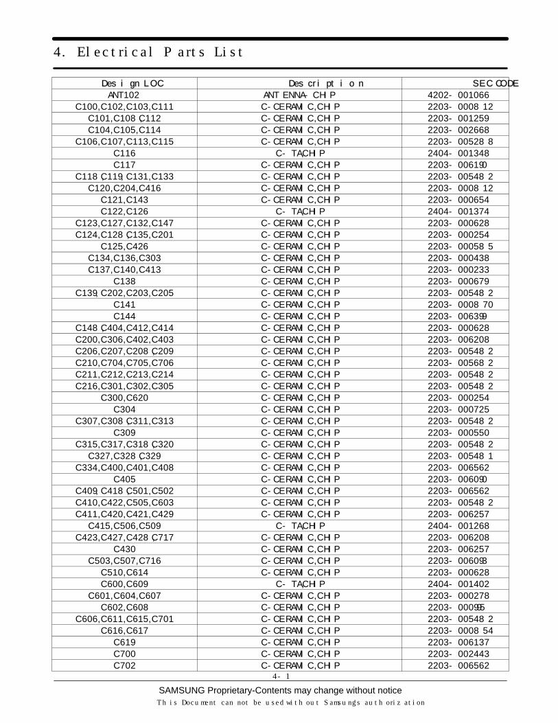
4. Electrical Parts List
4-1
This Document can not be used without Samsung's authorization
Design LOC Description SEC CODE
ANT102 ANTENNA-CHIP 4202-001066
C100,C102,C103,C111 C-CERAMIC,CHIP 2203-000812
C101,C108,C112 C-CERAMIC,CHIP 2203-001259
C104,C105,C114 C-CERAMIC,CHIP 2203-002668
C106,C107,C113,C115 C-CERAMIC,CHIP 2203-005288
C116 C-TA,CHIP 2404-001348
C117 C-CERAMIC,CHIP 2203-006190
C118,C119,C131,C133 C-CERAMIC,CHIP 2203-005482
C120,C204,C416 C-CERAMIC,CHIP 2203-000812
C121,C143 C-CERAMIC,CHIP 2203-000654
C122,C126 C-TA,CHIP 2404-001374
C123,C127,C132,C147 C-CERAMIC,CHIP 2203-000628
C124,C128,C135,C201 C-CERAMIC,CHIP 2203-000254
C125,C426 C-CERAMIC,CHIP 2203-000585
C134,C136,C303 C-CERAMIC,CHIP 2203-000438
C137,C140,C413 C-CERAMIC,CHIP 2203-000233
C138 C-CERAMIC,CHIP 2203-000679
C139,C202,C203,C205 C-CERAMIC,CHIP 2203-005482
C141 C-CERAMIC,CHIP 2203-000870
C144 C-CERAMIC,CHIP 2203-006399
C148,C404,C412,C414 C-CERAMIC,CHIP 2203-000628
C200,C306,C402,C403 C-CERAMIC,CHIP 2203-006208
C206,C207,C208,C209 C-CERAMIC,CHIP 2203-005482
C210,C704,C705,C706 C-CERAMIC,CHIP 2203-005682
C211,C212,C213,C214 C-CERAMIC,CHIP 2203-005482
C216,C301,C302,C305 C-CERAMIC,CHIP 2203-005482
C300,C620 C-CERAMIC,CHIP 2203-000254
C304 C-CERAMIC,CHIP 2203-000725
C307,C308,C311,C313 C-CERAMIC,CHIP 2203-005482
C309 C-CERAMIC,CHIP 2203-000550
C315,C317,C318,C320 C-CERAMIC,CHIP 2203-005482
C327,C328,C329 C-CERAMIC,CHIP 2203-005481
C334,C400,C401,C408 C-CERAMIC,CHIP 2203-006562
C405 C-CERAMIC,CHIP 2203-006090
C409,C418,C501,C502 C-CERAMIC,CHIP 2203-006562
C410,C422,C505,C603 C-CERAMIC,CHIP 2203-005482
C411,C420,C421,C429 C-CERAMIC,CHIP 2203-006257
C415,C506,C509 C-TA,CHIP 2404-001268
C423,C427,C428,C717 C-CERAMIC,CHIP 2203-006208
C430 C-CERAMIC,CHIP 2203-006257
C503,C507,C716 C-CERAMIC,CHIP 2203-006093
C510,C614 C-CERAMIC,CHIP 2203-000628
C600,C609 C-TA,CHIP 2404-001402
C601,C604,C607 C-CERAMIC,CHIP 2203-000278
C602,C608 C-CERAMIC,CHIP 2203-000995
C606,C611,C615,C701 C-CERAMIC,CHIP 2203-005482
C616,C617 C-CERAMIC,CHIP 2203-000854
C619 C-CERAMIC,CHIP 2203-006137
C700 C-CERAMIC,CHIP 2203-002443
C702 C-CERAMIC,CHIP 2203-006562

SAMSUNG Proprietary-Contents may change without notice
Electrical Parts List
4-2
This Document can not be used without Samsung's authorization
Design LOC Description SEC CODE
C707,C708,C709,C710 C-CERAMIC,CHIP 2203-005682
C711,C718,C719,C720 C-CERAMIC,CHIP 2203-005682
C712,C713 C-CERAMIC,CHIP 2203-006423
C714,C715 C-CERAMIC,CHIP 2203-005065
C721,C722,C723,C724 C-CERAMIC,CHIP 2203-005682
C725,C726,C727,C728 C-CERAMIC,CHIP 2203-005682
C729 C-CERAMIC,CHIP 2203-005682
CN100 CONNECTOR-COAXIAL 3705-001242
CN500 CONNECTOR-SOCKET 3710-001994
CN501 CONNECTOR-HEADER 3711-005781
CN601 JACK-PHONE 3722-002010
CN700 CONNECTOR-HEADER 3711-005938
CN704 CONNECTOR-HEADER 3711-005818
D500 DIODE-ZENER 0403-001427
F101 FILTER-EMI SMD 2901-001254
L101 INDUCTOR-SMD 2703-002170
L103 INDUCTOR-SMD 2703-002314
L104,L105,L109,L110 INDUCTOR-SMD 2703-002365
L106 INDUCTOR-SMD 2703-002281
L107 INDUCTOR-SMD 2703-002596
L108 INDUCTOR-SMD 2703-002208
L111 INDUCTOR-SMD 2703-001752
L400 CORE-FERRITE BEAD 3301-001120
L401 INDUCTOR-SMD 2703-002840
L402,R103,R113,R118 R-CHIP 2007-000171
L700 CORE-FERRITE BEAD 3301-001534
L701 CORE-FERRITE BEAD 3301-001342
LED700,LED701,LED702 LED 0601-002055
LED703,LED704,LED705 LED 0601-002055
LED706,LED707,LED708 LED 0601-002055
LED709,LED710,LED711 LED 0601-002055
LED712,LED713,LED715 LED 0601-002055
LED717,LED718,LED719 LED 0601-002055
LED720,LED721,LED722 LED 0601-002055
LED723 LED 0601-002055
MODULE1 FILTER 2911-000007
OSC100 OSCILLATOR-VCTCXO 2809-001281
OSC400 CRYSTAL-UNIT 2801-004373
Q100,Q101,Q102,Q103 TR-DIGITAL 0504-001151
Q500 TR-DIGITAL 0504-001151
Q700 ;SI1902DL 0505-001469
R100,R101,R102,R104 R-CHIP 2007-000162
R105 R-CHIP 2007-000173
R108,R200,R307,R505 R-CHIP 2007-000148
R110,R117 R-CHIP 2007-000138
R120,R126,R127,R135 R-CHIP 2007-000171
R121,R125 R-CHIP 2007-007014
R122,R124,R128,R131 R-CHIP 2007-000170
R123 R-CHIP 2007-001303
R201,R208,R300,R308 R-CHIP 2007-000171

SAMSUNG Proprietary-Contents may change without notice
Electrical Parts List
4-3
This Document can not be used without Samsung's authorization
Design LOC Description SEC CODE
R203,R204,R600,R603 R-CHIP 2007-000242
R205 R-NETWORK 2011-001394
R206 R-CHIP 2007-000143
R301 R-CHIP 2007-001325
R303,R306,R404,R501 R-CHIP 2007-000162
R309,R318,R403,R407 R-CHIP 2007-000171
R400 R-CHIP 2007-007592
R401,R512 R-CHIP 2007-007334
R402 R-CHIP 2007-007100
R408,R518,R519,R520 R-CHIP 2007-000171
R409,R604,R608 R-CHIP 2007-002796
R500,R502 R-CHIP 2007-000758
R503,R504,R609,R700 R-CHIP 2007-000162
R506 R-CHIP 2007-000152
R507 C-CERAMIC,CHIP 2203-005061
R508,R509 R-CHIP 2007-000170
R510,R611 R-CHIP 2007-007573
R511 R-CHIP 2007-000137
R513 R-CHIP 2007-008275
R514 R-CHIP 2007-007489
R515,R516 R-CHIP 2007-000172
R602,R606,R725 R-CHIP 2007-000148
R605,R607 R-CHIP 2007-000242
R610 R-CHIP 2007-001339
R612 R-CHIP 2007-007480
R701,R702,R703,R704 R-CHIP 2007-002970
R705,R706,R707,R708 R-CHIP 2007-002970
R709,R710,R711,R712 R-CHIP 2007-002970
R713,R714,R727,R729 R-CHIP 2007-002970
R717 R-CHIP 2007-000162
R721,R722 R-CHIP 2007-007317
R730 R-CHIP 2007-000171
R731,R732,R733,R734 R-CHIP 2007-002970
R790,R791 R-CHIP 2007-002970
SIM400 CONNECTOR-CARD EDGE 3709-001384
U100 IC 1205-002709
U101 IC 1201-002223
U103,U303 IC 0801-002237
U200 IC 1205-002647
U300 COMP-SMD GH13-00030A
U301 MEMORY 1108-000022
U302 IC 1204-002138
U304 IC 1209-001618
U306 IC 0801-002882
U400 IC 1203-003767
U401 IC 1203-002837
U402 IC 1203-003787
U404 BATTERY 4302-001177
U405 IC 1203-003568
U500 DIODE-TVS 0406-001188

SAMSUNG Proprietary-Contents may change without notice
Electrical Parts List
4-4
This Document can not be used without Samsung's authorization
Design LOC Description SEC CODE
U501,U700 IC 1203-003737
U502 FILTER-EMI SMD 2901-001315
U503 IC 1203-003742
U600 IC 1001-001333
U603 IC 1202-001068
U701 IC 1009-001010
U702 IC 1203-003046
U703 RF-MODULE 4709-001374
V300,V301,V302,V303 VARISTOR 1405-001082
V400,V701,V702,V703 VARISTOR 1405-001082
V500 THERMISTOR 1404-001221
V704,V705 VARISTOR 1405-001082
ZD500 DIODE-ZENER 0403-001547
ZD600,ZD601 DIODE-TVS 0406-001208
ZD701,ZD702,ZD703 DIODE-TVS 0406-001203

SAMSUNG Proprietary-Contents may change without noticeThis Document can not be used without Samsung's authorization
5. Block Diagrams
5-1
5-1. RF Solution Block Diagram

SAMSUNG Proprietary-Contents may change without notice
Block Diagrams
This Document can not be used without Samsung's authorization
5-2
5-2. Base Band Solution Block Diagram

SAMSUNG Proprietary-Contents may change without notice
6. PCB Diagrams
6-1
This Document can not be used without Samsung's authorization
6-1. PCB Top Diagram

SAMSUNG Proprietary-Contents may change without notice
PCB Diagrams
6-2
This Document can not be used without Samsung's authorization
6-2. PCB Bottom Diagram

SAMSUNG Proprietary-Contents may change without notice
7. Flow Chart of Troubleshooting
This Document can not be used without Samsung's authorization
7-36
7-1. Power On
Yes
Yes
Check the initial operation
Yes
No Check the clock generation circuit
(related to U100)
Check for the clock at C303
= 26MHz
Check the +VDD_GSM_CORE circuitC402(+VDD_GSM_CORE)
= 1.8V?
No
C430(+VDD_IO_LOW) &C429(+VDD_IO_HIGH) = "H"?
Yes
NoResolder OSC400
Check the Clock at
R402=32KHZ
Yes
NoChange the PMU (U405)
Yes
No
END
Change the Battery
' Power On ' does not work
Check the Battery Voltage
is more than 3.4V
Yes

SAMSUNG Proprietary-Contents may change without noticeThis Document can not be used without Samsung's authorization
Flow Chart of Troubleshooting
7-2
SIM_VC
C
SIM_C
LK
SIM_R
ST
Backup_B
attery
DC
/DC
Dow
n Conveter(1.8Volt)
SIM_IO
2.3T SIM
R400
C425
C411
C413
L401
C415
R404
GN
D2
MO
DE
61R
UN
3SW
VFB5
VIN4
R408
U401
+VDD
_IO_LO
W
R402
C412
V400
C414
R407
C429
NEG2
POS1
C418
U404
C424
L400
C419
C430
C416
C426
C403
C427
R409
R403
TP400
C420
C402
C421
C410
C428
C422
C423
C405
L402
C417
NC
910
NC
VCC
12R
ST
VCC
5
5000-6P-2.3M
SIM400
CLK
34G
ND
IO67
NC
NC
8
R401
OSC
400
21
44
_SIMRSHC
7 32
VINT
29VSAVE
30
_IRQ
10
_ONKEY
27
_REC1
1
_REC
213
_RSTHC11
_SIMR
SCD
SIMCKHC
8
SIMD
3VBA
T40
SIMEN
45
SIMIO
CD
42
SIMIOHC
9
SIMVC
C41
VBAT
31VCHG
28
RF12VB
AT
2322R
F1VDD
RF2VD
D24
SCL
2
SCN
38
SCP
37
SDA
3
SIMC
KC
D43
MICBIAS
12
NC
5354N
C
OSCI
26
OSCO
25
PWREN1
6 PWREN2
5REFC
48
GPO
247
GPO
346
18H
CVB
AT
HC
VDD
17
IOD
2VBA
T1514
IOVD
D
20LPD
1VBA
T
LPVDD
19
D1VD
D2116
D2VD
D
D3VD
D39
GN
D4950
GN
DG
ND
5152G
ND
GPO
1
U405
CHGCUR/BATMAX
34
CHGDRV
33
CLK32K
4
CPVBAT
36
CPVDD
35
C404
VBA
T+VD
D_G
SM_C
OR
E
REF_O
N+VD
D_IO
_LOW
IT_PMU
ON
KEYN
AU
X_ON
RSTO
N
SIMR
ST
+VDD
_RX_TX
+VCC
_SYN
+VDD
_IO_H
IGH
BU
_RST
32KH
z_DIG
IT
+VDD
_G_A
VDD
_SLEEP
VBA
T
+AVD
D_H
FA
+VDD
_IO_LO
W
+AVD
D
MIC
_BIA
S
REF_O
N
PON
_TX
SCLSD
A
SIMC
LK
SIMIO

SAMSUNG Proprietary-Contents may change without notice
Flow Chart of Troubleshooting
This Document can not be used without Samsung's authorization
7-3

SAMSUNG Proprietary-Contents may change without noticeThis Document can not be used without Samsung's authorization
Flow Chart of Troubleshooting
7-4
7-2. Initial
U200 pin 12 (RSTON)="H"
Initial Failure
Check the circuit related to reset
END
No
Yes
Is U200 R203, R204
OK?
Yes
Yes
NoCheck the U200
Check the 16bit data signal
Yes
Yes
Check the Battery Voltage
is more than 3.4V
NoChange the Battery
Yes
No
Check U405 pin 4 : 32MHz
Change the PMU

SAMSUNG Proprietary-Contents may change without notice
Flow Chart of Troubleshooting
This Document can not be used without Samsung's authorization
7-5

SAMSUNG Proprietary-Contents may change without noticeThis Document can not be used without Samsung's authorization
Flow Chart of Troubleshooting
7-6
7-3. Charging Part
Yes
Resolder or replace U503
Check the circuit related to
AUX_ON signal
Resolder or replace U503
Check the circuit related to
V_EXT_CHARGE
Yes
NoCheck the U503 pin 10
≒ 4.2V
Yes
No
U503 pin 3 = "L"?
Yes
No
U503 pin 5 = "L"?
Yes
No
END
Abnormal charging part
Check the U503 pin 1
> 4.9V

SAMSUNG Proprietary-Contents may change without notice
Flow Chart of Troubleshooting
This Document can not be used without Samsung's authorization
7-7
BATTERY CHARGING
R512
VBAT
R514
C504
3 _PPR
11GND
GND 8
9ICDL
6IMIN
USB2
USBON 7_CHG4
_EN5
U503
BAT 10CRDL
1ZD500
R510
C503
C506
C507
+VDD_IO_HIGH
C505
R511
R513
D500
END_OF_CHG
CHG_ON
AUX_ON
MES_BATTV_EXT_CHARGE
+VBUS
USB_CHG_ON

SAMSUNG Proprietary-Contents may change without noticeThis Document can not be used without Samsung's authorization
Flow Chart of Troubleshooting
7-8
7-4. Sim Part
SIM400 pin 1,5 = "H"?
Phone can't access SIM Card
Check the sim charge pump
Check the SIM Card
END
No
Yes
Yes
Yes
No
Check the Clock
After Power ON,
Check SIMCLK Signal on
pin3 of SIM400 in a few
Yes
No
Replace PBAAfter SIM card insert,
SIM400 pin 2 = "H(SIM_RST)"?
Yes

SAMSUNG Proprietary-Contents may change without notice
Flow Chart of Troubleshooting
This Document can not be used without Samsung's authorization
7-9
SIM_VCC
SIM_CLK
SIM_RST
Backup_Battery
SIM_IO
2.3T SIM
C425
C411
C413
C415
R404100K
R408
+VDD_IO_LOW
R402
C412
V400
C414
R407
C429N
EG2
POS
1
10V1000nFC418
U40
4
C424
C419
C430
C416
C426
C427
510R409
R403
TP400
C420
C421
C410
C428
C422C423
L402
C417
NC9
10 NC
VCC12 RST
VCC5
5000-6P-2.3M
SIM400
CLK34 GND
IO67 NC
NC8
OSC400
21
44
_SIM
RS
HC
7
32
VIN
T
29
VSA
VE
30
_IR
Q
10
_ON
KEY
27
_REC
1
1
_REC213_R
STH
C
11
_SIMRSCD
SIM
CK
HC
8
SIMD3VBAT 40
SIMEN 45
SIMIOCD 42
SIM
IOH
C
9
SIMVCC 41
VBA
T
31
VCH
G
28
RF12VBAT23
22 RF1VDD
RF2VDD24
SCL
2
SCN 38
SCP 37
SDA
3
SIMCKCD 43
MIC
BIA
S
12
NC 5354NC
OSC
I26
OSC
O
25
PWR
EN1
6
PWR
EN2
5
REF
C
48
GPO2 47
GPO3 46
18 HCVBAT
HCVDD17
IOD2VBAT15
14 IOVDD
20 LPD1VBAT
LPVDD19
D1VDD21
16 D2VDD
D3VDD 39
GND 4950GND
GND 5152GND
GPO1
U405
CH
GC
UR
/BA
TMA
X
34
CH
GD
RV
33
CLK
32K
4
CPV
BA
T
36
CPV
DD
35
IT_PMU
ONKEYN
AUX_ON
RSTON
SIMRST
+VDD_RX_TX
+VCC_SYN
+VDD_IO_HIGH
BU_RST
32KHz_DIGIT
+VDD_G_A
VDD_SLEEP
VBAT
+AVDD_HFA
+VDD_IO_LOW
+AVDD
MIC_BIAS
REF_ON
PON_TX
SCL
SDA
SIMCLK
SIMIO
SAMSUNG Proprietary-Contents may change without noticeThis Document can not be used without Samsung's authorization
Flow Chart of Troubleshooting
7-10
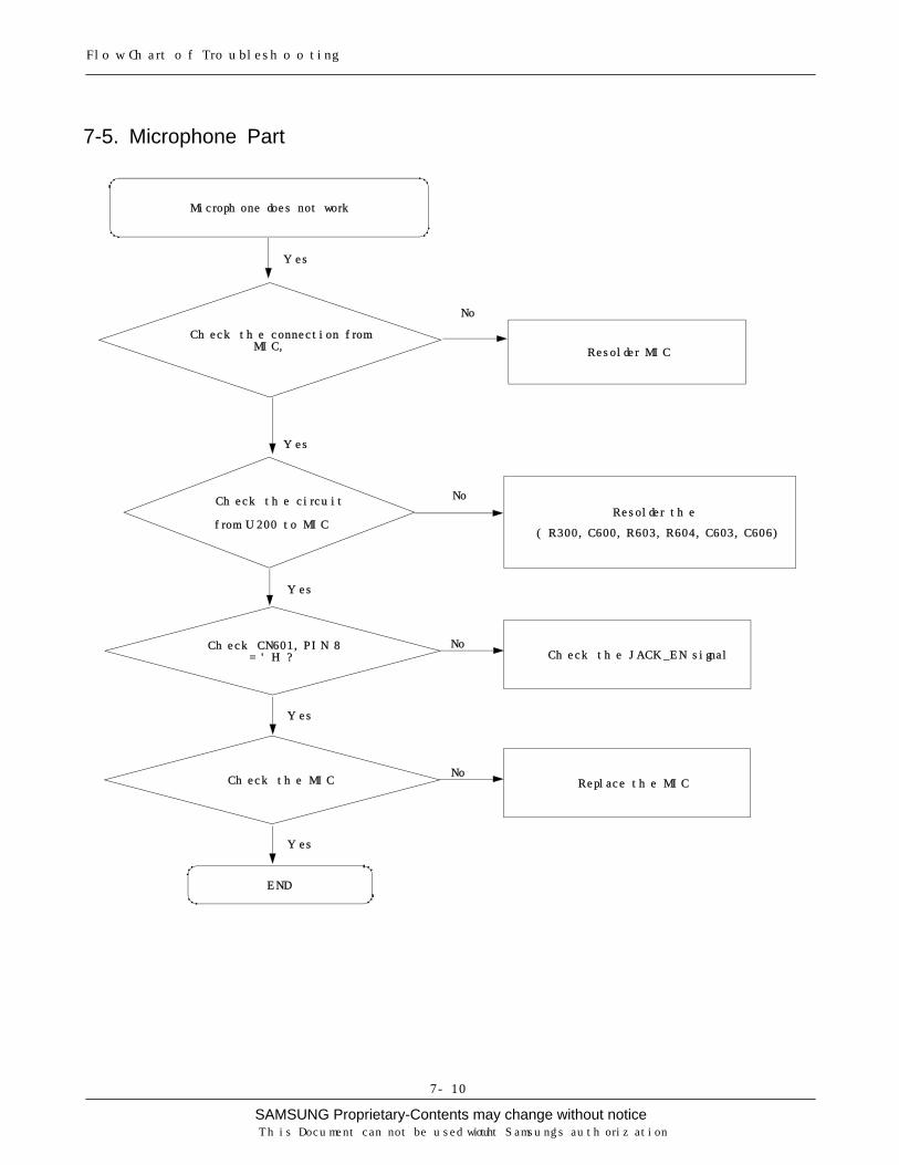
7-5. Microphone Part
Replace the MICNo
Check the MIC
Yes
Microphone does not work
Check the JACK_EN signalNoCheck CN601, PIN 8
= ' H' ?
No
Yes
Yes
Yes
Yes
No
END
Resolder the
(R300, C600, R603, R604, C603, C606)
Resolder MIC
Check the circuit
from U200 to MIC
Check the connection fromMIC,

SAMSUNG Proprietary-Contents may change without notice
Flow Chart of Troubleshooting
This Document can not be used without Samsung's authorization
7-11
MAIN_MIC
Close to MCP
Close to microphone
C602
C606
R603
C605 R602
R600
C604
C607ZD600
1 2 3
456
C608
MIC_BIAS
C603
R604
MIC600
C600C601
MIC_CP
MIC_N
MIC_P

SAMSUNG Proprietary-Contents may change without noticeThis Document can not be used without Samsung's authorization
Flow Chart of Troubleshooting
7-12
7-6. Speaker Part(Melody)
Check the U302Pin 3, 15
Speaker does not work
Check the U600 Pin 11(EAR1) Replace the U600
No
Yes
No
Check the U300
Resolder C311, C315
Yes
Check LCDconnector(CN700)PIN 37, 38
Resolder CN700
No
Yes
No
END
Check speakerSPK+, SPK-= Operate
Replace SPK
Yes
Yes
Check LCD Module Replace LCD Module
No
Yes

SAMSUNG Proprietary-Contents may change without notice
Flow Chart of Troubleshooting
This Document can not be used without Samsung's authorization
7-13
C306
R301
+VDD_IO_LOW
C303
C308
C307
C315
C304
+VDD_IO_HIGH
C311
C305 9VREF
8 VSS
/CS
29
3
/IRQ
/RD
31
/RST
4
28/W
R
5NC
PLLC6
17SPOUT1SPOUT2
18
15
SPVD
D
16
SPVS
S
7VDD
G3334
GG
35 36GH
POU
T-L/
MO
NO
10 11
HPO
UT-
R
IOVD
D
32
LED2
19MTR
24
23D4
D522
21D6
D720
EQ1
12 13
EQ2
EQ3
14
U302
30
A0
1CLKI
D0
27 26
D1
25D2
D3
HD(1)
HD(0)
26M_DIGIT
HA(1)
VIB
M_LED
HD(7)
HD(6)
HD(5)
HD(4)
HD(3)
HD(2)
WEn
RSTON
OEn
M_INT
CS5n_MELODY
ANL
ANR
C72
0
C71
8
C72
4
+VDD_IO_HIGH
C72
8
C70
8C
722
C70
9
VBAT
C72
1
C72
9
C70
5
C70
6
C70
7C713 C
710
C71
1
C71
9
C72
6
C72
7
C72
5
C712
8 89
9
3939
4 4
40404141 4242
5 566
7 7
3131 32323333 34343535 36363737 3838
2323 24242525 26262727 28282929
3 3
3030
16 1617 17 18 1819 19
22
20 202121 2222
1 1
1010
11 11 12 1213 13 14 1415 15
CN700
C70
4
C72
3
LCD_BL_ON
L_WR
LD(3)LD(4)LD(5)LD(6)LD(7)LD(8)LD(9)LD(10)LD(11)LD(12)LD(13)LD(14)LD(15)
HFR_PVIB
LD(0)LD(1)
LED_REDLED_GREEN
LED_BLUE
AMP_EN
MELODY_SEL
LD(2)
RS
LCD_MAIN_CS
HFR_N
LCD_SUB_CS
KEY_COL(0)
OLED_EN
KEY_ROW(4)

SAMSUNG Proprietary-Contents may change without noticeThis Document can not be used without Samsung's authorization
Flow Chart of Troubleshooting
7-14

SAMSUNG Proprietary-Contents may change without notice
Flow Chart of Troubleshooting
This Document can not be used without Samsung's authorization
7-15
7-7. Key Data Input
When one of the keys is
pushed,
Isn't it displayed on LCD?
Check the Dome sheet & Key Pad
END
No
Yes
Yes
Check Initial Operation
When one of the keys is
pushed,
KEY_ROW(0,4),KEY_COL(0,4)signal is OK?
Resolder V701,V702, 703, 704, 705& ZD701, ZD702, ZD703
No
Yes

SAMSUNG Proprietary-Contents may change without noticeThis Document can not be used without Samsung's authorization
Flow Chart of Troubleshooting
7-16
CAMERA_KEY
End_Key
VOLUME_KEYV7
02
4GND
5GND1
3V_COMMON
V_DOWN2
1V_UP
NEW_VOLUM_KEY2
VOL700
V703
END12
V705ZD
701
NEW_VOLUM_KEY_1
VOL701
3GND
1IN
2OUT
ZD70
3
ZD70
2
V704
V701
KEY_ROW(3)
KEY_ROW(4)
KEY_COL(1)
KEY_COL(0)
ONKEYN
KEY_ROW(3)

SAMSUNG Proprietary-Contents may change without notice
Flow Chart of Troubleshooting
This Document can not be used without Samsung's authorization
7-17

SAMSUNG Proprietary-Contents may change without noticeThis Document can not be used without Samsung's authorization
Flow Chart of Troubleshooting
7-18
7-8. Receiver Part
U600 EAR1, EAR2 = 1.5V? Resolder U200 or change PBA
END
No
Yes
Yes
Receiver does not work
LCD MODULESPK +,- PAD = 1.5V?
Change the LCD Module
No
Yes
No
Resolder CN700
Yes
Check LCD connectorCN700 pin 37, 38

SAMSUNG Proprietary-Contents may change without notice
Flow Chart of Troubleshooting
This Document can not be used without Samsung's authorization
7-19
VBAT
Y13
16 Y0
Y115
Z
2
Z0
3
Z1
1
_EN
A
4
GND
NC 5
NC
1819
NC
VCC14
12
X
10
X0X1
11
NLAS4783
U600
9
A
8B
7C
GND 6
17
EARSPK_L
EAR
SPK
_CO
M
EAR_MUTE
EAR
SPK
_R
EAR
1
EAR2
HFR
_N
C72
0
C71
8
C72
4
+VDD_IO_HIGH
C72
8
C70
8C
722
C70
9
VBAT
C72
1
C72
9
C70
5
C70
6
C70
7C713 C
710
C71
1
C71
9
C72
6
C72
7
C72
5
C712
8 89
9
3939
4 4
40404141 4242
5 566
7 7
3131 32323333 34343535 36363737 3838
2323 24242525 26262727 28282929
3 3
3030
16 1617 17 18 1819 19
22
20 202121 2222
1 1
1010
11 11 12 1213 13 14 1415 15
CN700
C70
4
C72
3
LCD_BL_ON
L_WR
LD(3)LD(4)LD(5)LD(6)LD(7)LD(8)LD(9)LD(10)LD(11)LD(12)LD(13)LD(14)LD(15)
HFR_PVIB
LD(0)LD(1)
LED_REDLED_GREEN
LED_BLUE
AMP_EN
MELODY_SEL
LD(2)
RS
LCD_MAIN_CS
HFR_N
LCD_SUB_CS
KEY_COL(0)
OLED_EN
KEY_ROW(4)

SAMSUNG Proprietary-Contents may change without noticeThis Document can not be used without Samsung's authorization
Flow Chart of Troubleshooting
7-20

SAMSUNG Proprietary-Contents may change without notice
Flow Chart of Troubleshooting
This Document can not be used without Samsung's authorization
7-21
7-9. Back Light (for Color Main LCD)
Is LCD Contrast set onhigh level in the Menu?
Set LCD Contrast on high level
END
No
Yes
Yes
Backlight does not work
IC8 pin 5 = H ?
Change the board to board
Connector
No
Yes
IC8 PIN 2 ≥ Vbat ? Check the IC8 & the related circuit
No
Yes
Yes
Replace the LCD Module

SAMSUNG Proprietary-Contents may change without noticeThis Document can not be used without Samsung's authorization
Flow Chart of Troubleshooting
7-22

SAMSUNG Proprietary-Contents may change without notice
Flow Chart of Troubleshooting
This Document can not be used without Samsung's authorization
7-23
7-10. Key Back Light
U700 pin 3, 6 = "H"? Check the U200 related to "KEY_LED_ON"
END
No
Yes
Yes
Main Key LED does not work
R71256
R71156
VOUT
56R710
U700CE6
GND25 GND
NC4
VDD 1
3
LED710
56R704
LED706
56R727
LED713 LED715
10V1000nFC702 R791
LED723
56R79056
LED722
56R706 R714
56
LED711LED701
R70956 56
R713
LED719LED718
R70356 56
R729
LED717LED712LED703LED704
56R705
LED702
56R708
LED700 LED708LED707
R7345656
R733
LED721
R70156 56
R731R70256
R70756 56
LED720
VBAT
R732
LED709LED705
KEY_LED_ON

SAMSUNG Proprietary-Contents may change without noticeThis Document can not be used without Samsung's authorization
Flow Chart of Troubleshooting
7-24
7-11. Camera part
"Camera" function does not work
Yes
No
Reconnect the camera module (CN704)Check the Camera
connector
Yes
CN 704 Pin 1, 20 = 2.8V?
No
Check the U405 ( or IC5)
Yes
END
CN704 Pin 17, 19 = 2.8V?
Yes
No
Check the U405 ( or I²C)
CN 704 Pin 1, 20 = 2.8V?
Yes
No
Replace the Camera Module
Check the camera module Change the PBA
No
Yes

SAMSUNG Proprietary-Contents may change without notice
Flow Chart of Troubleshooting
This Document can not be used without Samsung's authorization
7-25
SIM_VCC
SIM_CLK
SIM_RST
Backup_Battery
SIM_IO
2.3T SIM
C425
C411
C413
C415
R404100K
R408
+VDD_IO_LOW
R402
C412
V400
C414
R407
C429
NEG
2PO
S1
10V1000nFC418
U40
4
C424
C419
C430
C416
C426
C427
510R409
R403
TP400
C420
C421
C410
C428
C422C423
L402
C417
NC9
10 NC
VCC12 RST
VCC5
5000-6P-2.3M
SIM400
CLK34 GND
IO67 NC
NC8
OSC400
21
44
_SIM
RS
HC
7
32
VIN
T
29
VSA
VE
30
_IR
Q
10
_ON
KEY
27
_REC
1
1
_REC213
_RST
HC
11
_SIMRSCD
SIM
CK
HC
8
SIMD3VBAT 40
SIMEN 45
SIMIOCD 42
SIM
IOH
C
9
SIMVCC 41
VBA
T
31
VCH
G
28
RF12VBAT23
22 RF1VDD
RF2VDD24
SCL
2
SCN 38
SCP 37
SDA
3
SIMCKCD 43
MIC
BIA
S
12
NC 5354NC
OSC
I26
OSC
O
25
PWR
EN1
6PW
REN
25
REF
C
48
GPO2 47
GPO3 46
18 HCVBAT
HCVDD17
IOD2VBAT15
14 IOVDD
20 LPD1VBAT
LPVDD19
D1VDD21
16 D2VDD
D3VDD 39
GND 4950GND
GND 5152GND
GPO1
U405
CH
GC
UR
/BA
TMA
X
34
CH
GD
RV
33
CLK
32K
4
CPV
BA
T
36
CPV
DD
35
IT_PMU
ONKEYN
AUX_ON
RSTON
SIMRST
+VDD_RX_TX
+VCC_SYN
+VDD_IO_HIGH
BU_RST
32KHz_DIGIT
+VDD_G_A
VDD_SLEEP
VBAT
+AVDD_HFA
+VDD_IO_LOW
+AVDD
MIC_BIAS
REF_ON
PON_TX
SCL
SDA
SIMCLK
SIMIO
1.3M 1/4 LSI Senser(0.9T)
667 78 8
99
27GG
28
222223 2324 2425 252626
3 34 455
15 1516 1617171818
19 19
22
20 202121
CN70411
101011 1112 12
13131414
CAM1.5V
R72
1
L701
CAM2.8V
CAM2.8V
R72
2
+VDD_IO_HIGH
R73
0
Y(5)
PCLK
Y(7)
Y(6)
Y(0)
Y(2)
M_SCLMCLKM_SDAS_RESET
FVALIDLVALID
FLASH_OUT
Y(1)
Y(3)
Y(4)

SAMSUNG Proprietary-Contents may change without noticeThis Document can not be used without Samsung's authorization
Flow Chart of Troubleshooting
7-26

SAMSUNG Proprietary-Contents may change without notice
Flow Chart of Troubleshooting
This Document can not be used without Samsung's authorization
7-27
7-13. BLUETOOTH
BLUETOOTH does not work
Yes
R126 = 'H'
No
Check the U200
Yes
Replace ANT102
No
Replace U703
Yes
END

SAMSUNG Proprietary-Contents may change without notice
Flow Chart of Troubleshooting
This Document can not be used without Samsung's authorization
7-28
7-13. GSM Receiver
Module1 pin8>= -65dBm Resolder CN100, C103
No
Yes
RX ONRF input : 62CH
Amp : -50dBm
Check Module1pin9,pin10,pin12 = L
Module1 pin1, pin2>= -65dBm
Check ANT Switchcontrol circuit
Resolder Module1
Yes
Yes
No No
END
U100 H7,H8,J7,J8>= 1V
U100E1 >= -70dBmF1 >= -70dBm
Resolder C108, C112, L107
Check U100J2,A6,B6,A9,E9>=2.7V
Check & ResolderU100, R117
RF26MHz, RF PSU Part
Resolder U100
C142, C146>= 1V
Yes
Yes
Yes
Yes
Yes
No
No No
Check U200

SAMSUNG Proprietary-Contents may change without notice
Flow Chart of Troubleshooting
This Document can not be used without Samsung's authorization
7-29
7-14. GSM Transmitter
Module1 Pin8>= 20dBm
Resolder CN100, C103
TX ON (5Level)
Check Module1pin10 = H (2.68V),pin9, pin12 = L
Module1 pin11>= 18dBm
U101 pin8>= 18dBm
U101 7pin>= -11dBm
Change or ResolderModule1
Check ANT Switchcontrol circuit
Resolder R122, L106
Yes
Check U101+VBAT, pin4, pin6
OK?Resolder or Change U101
Check +VBAT or U101control signal
No
No
No
No
Yes
Yes
Yes
Yes
Yes
No
Yes
No
NoNoCheck & ResolderU100, R117
RF26MHz, RF PSU Part
Check U100J2,A6,B6,A9,E9>=2.7V
U100 H7,H8,J7,J8>= 1V
YesYesResolder U100
Check U200
END

SAMSUNG Proprietary-Contents may change without noticeThis Document can not be used without Samsung's authorization
Flow Chart of Troubleshooting
7-30
7-15. DCS Receiver
Module1 Pin8>= -65dBm Resolder CN100, C103
No
Yes
RX ONRF input : 698CH
Amp : -50dBm
Check Module1pin9,pin10,pin12 = L
Module1 pin3, pin4>= -65dBm
U100D1 >= -70dBmC1 >= -70dBm
Check ANT Switchcontrol circuit
Resolder Module1
Resolder C105, C106, L104, L105
Yes
Yes
Yes
No
No
No
END
U100 H7,H8,J7,J8>= 1V
Check U100J2,A6,B6,A9,E9>=2.7V
Check & ResolderU100, R117
RF26MHz, RF PSU Part
Resolder U100
C142, C146>= 1V
Yes
Yes
Yes
Yes
No No
Check U200

SAMSUNG Proprietary-Contents may change without notice
Flow Chart of Troubleshooting
This Document can not be used without Samsung's authorization
7-31
7-16. DCS Transmitter
Module1 pin8>= 20dBm Resolder CN100, C103
TX ON (0Level)
Check Module1pin12 = H (2.68V),pin9, pin10 = L
Module1 pin13>= 18dBm
U101 pin9>= 18dBm
U101 pin1>= -11dBm
Change or ResolderModule1
Check ANT Switchcontrol circuit
Resolder C109, L108, C113
Yes
Check U101+VBAT, pin4, pin6
OK?Resolder or Change U101
Check +VBAT or U101control signal
No
No
No
No
No
Yes
Yes
Yes
Yes
Yes
No
Yes
U100 H7,H8,J7,J8>= 1V
Check & ResolderU100, R117
RF26MHz, RF PSU Part
Yes
No No
END
Check U200
Resolder U100Yes
Check U100J2,A6,B6,A9,E9
>=2.7VOK?

SAMSUNG Proprietary-Contents may change without noticeThis Document can not be used without Samsung's authorization
Flow Chart of Troubleshooting
7-32
7-17. PCS Receiver
Module1 pin8>= -65dBm Resolder CN100, C103
No
Yes
RX ONRF input : 661CH
Amp : -50dBm
Check Module1pin9= H
pin10, pin12 = L
Module1 pin5, pin6>= -65dBm
U100B1 >= -70dBmA1 >= -70dBm
Check ANT Switchcontrol circuit
Resolder Module1
Resolder C114, C115, L109, L110
Yes
YesYes
No
No
No
END
U100 H7,H8,J7,J8>= 1V
Check U100J2,A6,B6,A9,E9>=2.7V
Check & ResolderU100, R117
RF26MHz, RF PSU Part
Resolder U100
C142, C146>= 1V
Yes
Yes
Yes
Yes
No No
Check U200

SAMSUNG Proprietary-Contents may change without notice
Flow Chart of Troubleshooting
This Document can not be used without Samsung's authorization
7-33
7-18. PCS Transmitter
Module1 Pin8>= 20dBm Resolder CN100, C103
TX ON (0Level)
Check Module1pin12 = H (2.68V),pin9, pin10 = L
Module1 pin13>= 18dBm
U101 pin9>= 18dBm
U101 pin1>= -11dBm
Change or ResolderModule1
Check ANT Switchcontrol circuit
Resolder L102, L108, C113
Yes
Check U101+VBAT, pin4, pin6
OK?Resolder or Change U101
Check +VBAT or U101control signal
No
No
No
No
No
Yes
Yes
Yes
Yes
Yes
No
Yes
U100 H7,H8,J7,J8>= 1V
Check & ResolderU100, C147, R117
RF26MHz, RF PSU Part
Yes
No No
END
Check U200
Resolder U100Yes
Check U100J2,A6,B6,A9,E9
>=2.7VOK?

SAMSUNG Proprietary-Contents may change without noticeThis Document can not be used without Samsung's authorization
Flow Chart of Troubleshooting
7-34
NC
C142
1M R122
C101
R124
1M
C117
C137
C143
C105
L105
+VCC
_SYN
AN
T100
C115
C135
C104
0.5PF50V
50VC
1361N
F
E1
E24
VBA
T
Q101
B1
25B
2
6C
1
C2
3 1
PEMD
10
L102
C108
C119
R113
R104
3G
ND
2IN N
C1
4O
UT
5VC
C
L101
U103
R112
TP100
R131
1M
C132
0R
135
+VDD
_IO_H
IGH
C147
2
13
R100
F101
AN
T101
C140
C122
C120
C116
E2
C112
2B
15
B2
C1
6
3C
2
E11
4
G1
34 G
2G
3
5G
4
6
1IN
2O
UT
PEMD
10
Q102
CN
100
CR
S5001-1702
+VCC
_SYN
C126
C1
6
3C
2
1E1
4E2
+VDD
_IO_H
IGH
R118
Q100
PEMD
10
2B
15
B2
L107
C123
C127
R121
R108
+VDD
_IO_H
IGH
1PFC
113
50V
2.2nHL108
C125
C106
R120
+VDD
_IO_H
IGH
50V1PF
C107
L110
R127
+VDD
_RX_TX
+VCC
_SYN
7
5PC
S_RX1
PCS_R
X26
VC1
10 12VC
2VC
39
MO
DU
LE18A
NT
3D
CS_R
X1D
CS_R
X24
13D
CS|PC
STX
EGSM
TX11
1EG
SM_R
X1EG
SM_R
X22
G
L109
R102
R117
VDD
_SLEEP
C131
5.6nH
C133
L106
R111
1MR
128
R123
C114
R110
C121
8TXEN
34VB
ATT
VRA
MP
6
1NF
C134
50V
U101
2B
AN
D1
DC
S/PCSIN
9D
CS/PC
SOU
TG
ND
10
5G
ND
7G
SMIN
GSM
OU
T
C124
OU
T3 4
VCC
VCO
N1O
SC100
2G
ND
C100
C102
R125
C111
R103
+VCC
_SYN
0
L103
C148
C110
R101
L104
E1
E24
R107
Q103
PEMD
10
B1
2B
25 6
C1
C2
3 1
C146
NC
C109
NC
J2VC
CO
PLL
J3VC
CTXVC
O
J4TXO
UTD
J5TXO
UTG
J6G
ND
TXVCO
G2
J7IO
UT/IIN
J8Q
OU
T/QIN
J9G
ND
MA
SH
H3
GN
DTXVC
OD
H4
GN
DTXVC
OB
H5
GN
DTXVC
OG
1
H6
VCC
TXVCO
G
H7
IOU
TB/IIN
B
H8
QO
UTB
/QIN
B
H9
LE
J1G
ND
LNA
F8C
LK
F9SD
ATA
G1
GSM
0LNA
IG
SM0G
ND
G2
G8
VCC
MA
SH
G9
CLK
OU
T1
H1
GSM
0LNA
IB
H2
GN
DO
PLL
D8
DIVO
N
D9
CLK
OU
T2
E1G
SM1LN
AI
E2G
ND
E8G
ND
CLK
E9VC
CC
LK
F1G
SM1LN
AIB
F2G
SM1G
SM0G
ND
B9
TCXO
IN
C1
DC
SLNA
I
C2
PCSD
CSG
ND
C3
GN
D
C8
CLK
2CO
NT
C9
GN
DB
UF2
D1
DC
SLNA
IB
D2
DC
SGSM
1GN
D
B1
PCSLN
AIB
B2
PCSG
ND
B3
VCC
MIX
B4
CA
PIB
B5
CA
PQB
B6
VCC
RFVC
O
B7
GN
DR
FSYN
B8
GN
DB
UF1
A2
GN
D
A3
VCC
LNA
A4
CA
PI
A5
CA
PQ
A6
VCC
RFLO
A7
VCC
BB
A8
VCC
RFSYN
A9
VCC
BU
F
U100
1N
C2
NC
A1
PCSLN
AI
C128
C118
C103
22
R106
R105
D_R
EF_CLK
TXON
PCS_R
X_NPC
S_RX_P
EGSM
_RX_P
EGSM
_RX_N
RX_TX_Q
P
RX_TX_Q
N
RX_TX_IP
RX_TX_IN
VC2
VC1
26M_D
IGIT
DC
S_RX_P
RF_C
LK
RF_D
ATA
RF_EN
AFC
VC3
J_AN
T
PCS_R
X_P
PCS_R
X_N
DC
S_RX_P
DC
S_RX_N
EGSM
_RX_P
EGSM
_RX_N
DC
S
RA
MP
DC
S_RX_N

SAMSUNG Proprietary-Contents may change without notice
Flow Chart of Troubleshooting
This Document can not be used without Samsung's authorization
7-35

SAMSUNG Proprietary-Contents may change without noticeThis Document can not be used without Samsung's authorization
Flow Chart of Troubleshooting
7-36