gsm telephone - sgh-f500 - Altehandys.de
117
GSM TELEPHONE SGH-F500 GSM TELEPHONE CONTENTS 1. Specification 2. Exploded View and Parts list 3. Chart of Troubleshooting 4. Array course control 5. Block Diagrams 6. PCB Diagrams 7. MAIN Electrical Parts List 8. Reference data 9. Safety Precautions 10. Product Function
-
Upload
khangminh22 -
Category
Documents
-
view
0 -
download
0
Transcript of gsm telephone - sgh-f500 - Altehandys.de
GSM TELEPHONESGH-F500
GSM TELEPHONE CONTENTS
1. Specification
2. Exploded View and Parts list
3. Chart of Troubleshooting
4. Array course control
5. Block Diagrams
6. PCB Diagrams
7. MAIN Electrical Parts List
8. Reference data
9. Safety Precautions
10. Product Function

Contents
1. Specification1-1. GSM General Specification .......................................................................................1-11-2. GSM TX power class ...............................................................................................1-2
2. Exploded View and Parts list2-1. Cellular phone Exploded View ..................................................................................2-12-2. Cellular phone Parts list ............................................................................................2-22-3. Disassembly ...............................................................................................................2-92-4. Assembly ..................................................................................................................2-11
3. Chart of Troubleshooting3-1. Baseband ............................................................................................................3-1
3-1-1. Power ON .....................................................................................................3-13-1-2. System Initial ................................................................................................3-53-1-3. SIM Part .......................................................................................................3-83-1-4. Charging Part .............................................................................................3-103-1-5. Microphone Part .........................................................................................3-123-1-6. Speaker Part ..............................................................................................3-153-1-7. Camera Part ..............................................................................................3-183-1-8. LCD .............................................................................................................3-21
3-2. RF ......................................................................................................................3-133-2-1. EGSM Rx ...................................................................................................3-233-2-2. DCS Rx ......................................................................................................3-243-2-3. PCS Rx ......................................................................................................3-253-2-4. EGSM Tx ...................................................................................................3-273-2-4. DCS & PCS Tx .........................................................................................3-283-2-6. BLUETOOTH ..............................................................................................3-30

Contents
4. Array course control4-1. Downloading Binary Files ......................................................................................4-24-2. Pre-requsite for Downloading ................................................................................4-24-3. S/W Downloader Program .....................................................................................4-3
5. Block Diagrams
6. PCB Diagrams
7. MAIN Electrical Parts List
8. Reference data8-1. Reference Abbreviate ..............................................................................................8-1
9. Safety Precautions9-1. Repair Precaution ......................................................................................................9-19-2. ESD(Electrostaically Sensitive Devices) Precaution ................................................9-2
10. Product Function

SAMSUNG Proprietary-Contents may change without notice
1. Specification
1-1
This Document can not be used without Samsung's authorization
1-1. GSM/WCDMA General Specification
EGSM 900Phase 2
DCS1800Phase 1 PCS1900 WCDMA
Freq. Band[MHz]Upl ink/Downl ink
880~915925~960
1710~17851805~1880
1850~19101930~1990
1920~19802110~2170
ARFCN range 0~124 &975~1023 512~885 512~810 10562~10838
Tx/Rx spacing 45 MHz 95 MHz 80 MHz 190 MHz
Mod. Bit rate/Bit Per iod
270.833 kbps3.692 us
270.833 kbps3.692 us
270.833 kbps3.692 us 3.84 Mcps/s
Time SlotPer iod/Frame
Period
576.9 us4.615 ms
576.9 us4.615 ms
576.9 us4.615 ms 10 ms
Modulat ion 0.3 GMSK 0.3 GMSK 0.3 GMSK UL:2BPSKDL:QPSK
MS Power 33 dBm~5 dBm 30 dBm~0 dBm 30 dBm~0 dBm MAX:24(+1,-3) dBmMIN:<-50 dBm
Power Class 5 pcl ~ 19 pcl 0 pcl ~ 15 pcl 0 pcl ~ 15 pcl CLASS3
Sensi t iv i ty -102 dBm -100 dBm -100 dBm -106.7 dBm
TDMA Mux 8 8 8 -
Cel l Radius 35 Km 2 Km - -

SAMSUNG Proprietary-Contents may change without notice
Specification
1-2
This Document can not be used without Samsung's authorization
1-2. GSM TX power class
TX Powercontrol level
EGSM900
5 33±2 dBm
6 31±2 dBm
7 29±2 dBm
8 27±2 dBm
9 25±2 dBm
10 23±2 dBm
11 21±2 dBm
12 19±2 dBm
13 17±2 dBm
14 15±2 dBm
15 13±2 dBm
16 11±3 dBm
17 9± 3dBm
18 7±3 dBm
19 5±3 dBm
TX Powercontrol level
DCS1800
0 30±3 dBm
1 28±3 dBm
2 26±3 dBm
3 24±3 dBm
4 22±3 dBm
5 20±3 dBm
6 18±3 dBm
7 16±3 dBm
8 14±3 dBm
9 12±4 dBm
10 10±4 dBm
11 8±4 dBm
12 6±4 dBm
13 4±4 dBm
14 2±5 dBm
15 0±5 dBm
TX Powercontrol level
PCS1900
0 30±3 dBm
1 28±3 dBm
2 26±3 dBm
3 24±3 dBm
4 22±3 dBm
5 20±3 dBm
6 18±3 dBm
7 16±3 dBm
8 14±3 dBm
9 12±4 dBm
10 10±4 dBm
11 8±4 dBm
12 6±4 dBm
13 4±4 dBm
14 2±5 dBm
15 0±5 dBm
SAMSUNG Proprietary-Contents may change without notice
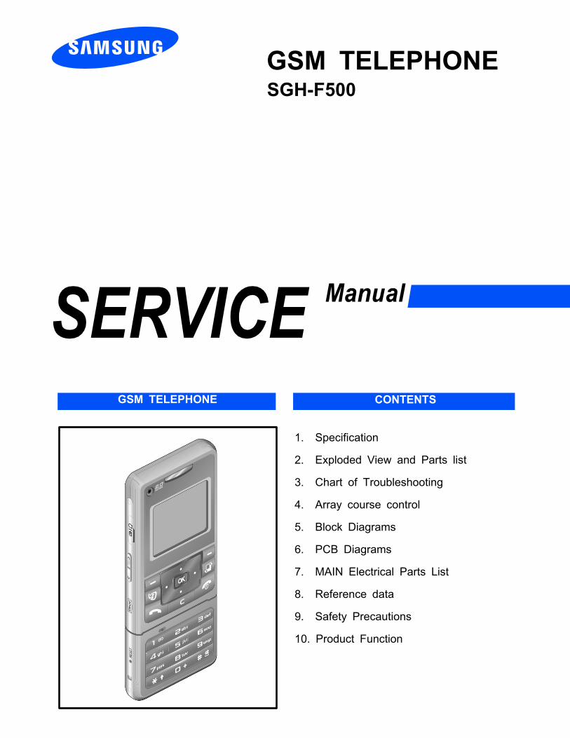
2. Exploded View and Parts List
2-1
This Document can not be used without Samsung's authorization
2-1. Cellular phone Exploded View
QKP01QKP01QSD01
QCK02
QCR67
QRF01
QBR18
QMI03
QMO01
QWD01QRF01
QCR67QRF03
QVO01QBR19
QCR03
QMC01
QKP02
QLC01
QBR02
QSP01
QCA01
QVK01
QCR12QAN05
QRE01
QLC02
QMW01
QCR03
QKP03
QHI17QFL01
QCK01
QHI01
QCR12
QBA01
QBR17
QME01
QKP01
QHI15
QCR05
QCR03
QCR05
QMP01
QME16
QCR12
QAN02
QCK03
+ QHI16 QHI01 QFL01 QCR12= +

SAMSUNG Proprietary-Contents may change without notice
Main Electrical Parts List
2-2
This Document can not be used without Samsung's authorization
Design LOC Discription SEC CODEQAN02 INTENNA-SGHF500 GH42-01094AQAN05 ASSY MEC-RUBBER ANT CON GH75-09161AQBA00 COVER BATTERY PACK-950MAH,BLK, GH43-02844AQBA01 INNER BATTERY PACK-880MAH,BLK, GH43-02588AQBR02 ASSY BRACKET-SUB GH98-03560AQBR17 ASSY BRACKET-BATT GH98-02339AQCA01 UNIT-PHONE CAMERA GH59-03593AQCK03 PMO-KEY TOUCH OK GH72-35526AQCR03 SCREW-MACHINE 6001-001811QCR03 SCREW-MACHINE 6001-001811QCR05 SCREW-MACHINE 6001-001478QCR05 SCREW-MACHINE 6001-001478QCR12 SCREW-MACHINE 6001-001530QCR67 SCREW-MACHINE 6001-002083QHI15 NDC-CASE SWING UPPER V2 GH71-07017AQKP01 ASSY KEYPAD-MAIN(OPEN/BLK) GH98-02861AQKP02 ASSY KEYPAD-SUB(OPEN/BLK) GH98-02860AQKP03 MEA-TOUCH KEYPAD KIT GH97-07638AQLC01 LCD-SGHF500 GH07-01032AQLC02 LCD-MODULE SGHF500 GH07-00992AQMC01 PMO-SIM COVER GH72-35542AQME01 UNIT-TF KEY PBA GH59-03767AQME16 UNIT-CON TO CON FPCB GH59-03792AQMI03 ASSY RUBBER-MIC HOLDER GH98-03682AQMO01 MOTOR DC-SPHB6400 GH31-00271AQMP01 PBA MAIN-SGHF500 GH92-03070AQMW01 ASSY COVER-WINDOW MAIN GH98-02870AQRE01 ASSY COVER-REAR GH98-02868AQRF01 PMO-COVER RF V2 GH72-35129AQSP01 SPEAKER 3001-002109QVK01 UNIT-SIDE KEY GH59-03762AQWD01 ASSY COVER-WINDOW SUB GH98-02869AQFR01 ASSY COVER-FRONT GH98-02863A QSD01 PMO-COVER MICRO SD GH72-35529A
QHI16 ASSY COVER-SWING LOWER GH98-05068A QCR12 SCREW-MACHINE 6001-001530 QFL01 ASSY CASE-SWING LOWER GH98-02337A QHI01 ASSY HINGE GH98-03747A
QHI17 ASSY COVER-SWING BELT GH98-05119A QCK01 PMO-CAMERA KEY GH72-33543A
QBR18 ASSY COVER-MAIN BELT R GH98-02864A QCK02 PMO-HOLD KEY GH72-35531A
QBR19 ASSY COVER-MAIN BELT L GH98-02865A QRF03 PMO-EAR JACK COVER GH72-35534A QVO01 PMO-VOLUME KEY GH72-33544A
2-2. Cellular phone Parts list

SAMSUNG Proprietary-Contents may change without notice
Main Electrical Parts List
2-3
This Document can not be used without Samsung's authorization
Discription SEC CODEIC-MEMORY CARD 1109-001363
CONNECTOR-ADAPTOR 3719-001319BAG PE 6902-000634
BAG ZIPPER 6902-000683CBF INTERFACE-AV CABLE GH39-00442A
CBF INTERFACE-DLC,X830,BLK,PCB GH39-00720AADAPTOR-SGHE690,BLK,EU,A_TYPE GH44-01361AS/W CD-SAMSUNG PC STUDIO 3.1,F GH46-00392AUNIT-EARPHONE,SGHE790,MAIN,A-T GH59-03884A
LABEL(P)-IMEI GH68-01335DLABEL(R)-WATER SOAK GH68-09361A
MANUAL USERS-EU DUTCH GH68-13752AMANUAL USERS-EU ENGLISH GH68-13753A
LABEL(R)-MAIN EU GH68-13981ABOX(P)-UNIT MAIN EU GH69-05089A
CUSHION-CASE TA2 MA1~2 GH69-05090AMPR-VINYL BOHO SIM CARD GH74-30419A
TAPE GASK GH74-31723AMPR-GASK TAPE GH74-31724AMPR-INSU TAPE GH74-31725A
TAPE-RF CONNECTOR GH74-31726ATAPE-IF CONNECTOR GH74-31727A
VINYL-BOHO MAIN KEY GH74-32568AVINYL-BOHO SUB KEY GH74-32569A
TAPE INSU-BOARD GH74-32936A

SAMSUNG Proprietary-Contents may change without notice
Main Electrical Parts List
2-4
This Document can not be used without Samsung's authorization
2-3. Disassembly1
3
2
4
1) DISASSEMBLE REAR ASS'YDisassemble REAR ASS'Y from the SET by using tools.
1) 2.4" LCD CONNECTOR REMOVEDisassemble 2.4" LCD CONNECTOR from PBA.※ caution1) NO DAMAGE to F-PCB
1) SCREW REMOVE 1Remove the 2POINT SCREWS on the both sides ofSET (SILVER 2 POINT)
1) SCREW REMOVE 2Remove the 3POINT SCREWS on the upper of SWINGpart. (BLACK 2 POINT, SILVER 1 POINT)

SAMSUNG Proprietary-Contents may change without notice
Main Electrical Parts List
2-5
This Document can not be used without Samsung's authorization
5 6
1) REMOVE THE RIGHT SIDE BELTRemove the SIDE BELT on the right of SET.
1) REMOVE THE LEFT SIDE BELTRemove the SIDE BELT on the left of SET.
7 8
1) DISASSEMBLE 2MEGA CAMERADisassemble the 2MEGA CAMERA combined withPBA
1) DISASSEMBLE VOLUME KEYDisassemble the VOLUME KEY F-PCB from theBODY.
SAMSUNG Proprietary-Contents may change without notice
Main Electrical Parts List
2-6
This Document can not be used without Samsung's authorization
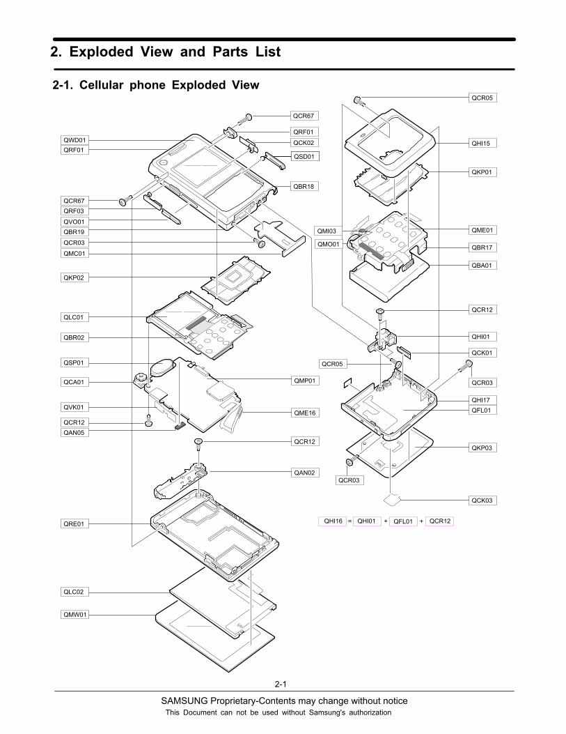
9 10
1) DISASSEMBLE SUB LCD CONNECTORDisassemble the SUB LCD CONNECTOR from thePBA.
1) REMOVE SCREWRemove the SCREW on the PBA.
11 12
1) DISASSEMBLE SPEAKERDisassemble the SPEAKER from the FRONTCOVER.
1) DISASSEMBLE PBA ASS'YDisassemble the PBA ASS'Y from the FRONTCOVER.
SAMSUNG Proprietary-Contents may change without notice
Main Electrical Parts List
2-7
This Document can not be used without Samsung's authorization
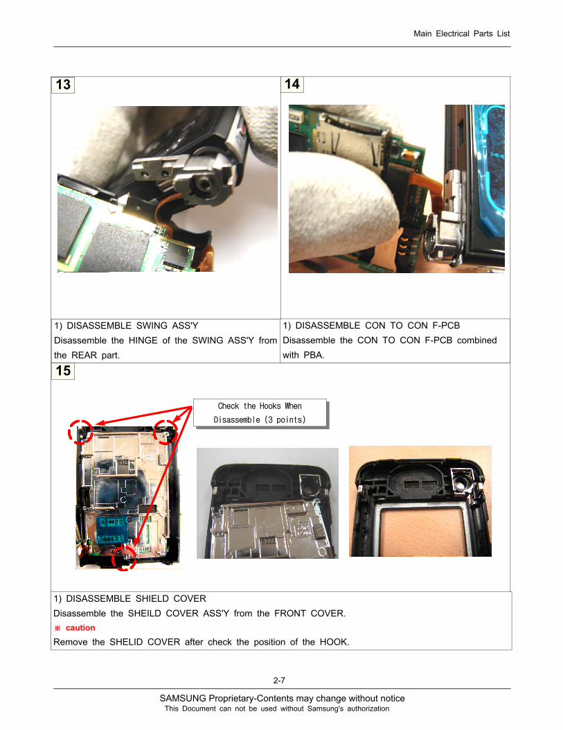
13 14
1) DISASSEMBLE SWING ASS'YDisassemble the HINGE of the SWING ASS'Y fromthe REAR part.
1) DISASSEMBLE CON TO CON F-PCBDisassemble the CON TO CON F-PCB combinedwith PBA.
15
1) DISASSEMBLE SHIELD COVERDisassemble the SHEILD COVER ASS'Y from the FRONT COVER.※ caution
Remove the SHELID COVER after check the position of the HOOK.
Check the Hooks When
Disassemble (3 points)

SAMSUNG Proprietary-Contents may change without notice
Main Electrical Parts List
2-8
This Document can not be used without Samsung's authorization
16 17
1) REMOVE SUB WINDOWREMOVE the SUB WINDOW from FRONT COVER
1) REMOVE 1.5" LCD MODULERemove the 1.5" LCD MODULE from SHIELDCOVER.
18 19
1) REMOVE SHIELD COVERRemove subsidiary material 2point combined with SHIELDCOVER
1) DISASSEMBLEINTENNADisassemble INTENNA after remove SCREWcombined with right side of INTENNA

SAMSUNG Proprietary-Contents may change without notice
Main Electrical Parts List
2-9
This Document can not be used without Samsung's authorization
20 21
1) REMOVE ELECTRIC CONDUCTION TAPERemove TAPE 2 POINT sticked with 2.4" LCD
1) REMOVE ELECTRIC CONDUCTION SPONGERemove sponge 2 POINT sticked with 2.4" LCD
22 23
1) DISASSEMBLE MAIN WINDOWDisassemble MAIN WINDOW from REAR ASS'Y
1) DISASSEMBLE 2.4" LCDDisassemble 2.4" LCD MODULE from rear part

SAMSUNG Proprietary-Contents may change without notice
Main Electrical Parts List
2-10
This Document can not be used without Samsung's authorization
24 25
1) REMOVE LABELRemove label sticked with upper of SWING ASS'Y
1) REMOVE SCREW 1Remove SCREW 1 POINT of SWING ASS'Y
26 27
1) REMOVE SCREW 2Remove SCREW 2 POINT on both side of SWINGASS'Y
1) UNCOVER TOUCH KEY CONNECTORUNCOVER ACTUATOR OF TOUCH KEYCONNECTOR
SAMSUNG Proprietary-Contents may change without notice
Main Electrical Parts List
2-11
This Document can not be used without Samsung's authorization
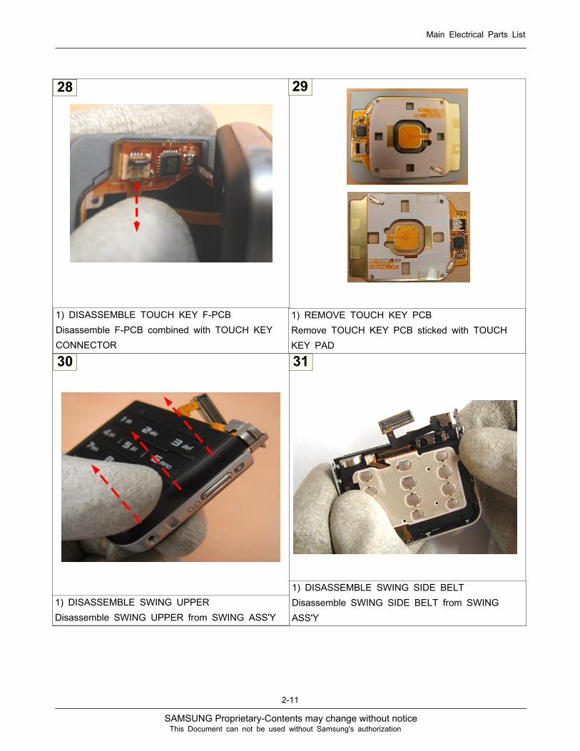
28 29
1) DISASSEMBLE TOUCH KEY F-PCBDisassemble F-PCB combined with TOUCH KEYCONNECTOR
1) REMOVE TOUCH KEY PCBRemove TOUCH KEY PCB sticked with TOUCHKEY PAD
30 31
1) DISASSEMBLE SWING UPPERDisassemble SWING UPPER from SWING ASS'Y
1) DISASSEMBLE SWING SIDE BELTDisassemble SWING SIDE BELT from SWINGASS'Y

SAMSUNG Proprietary-Contents may change without notice
Main Electrical Parts List
2-12
This Document can not be used without Samsung's authorization
32 33
1) DISASSEMBLE CON TO CON F-PCBDisassemble CON TO CON F-PCB between hinge※ cautionNO DAMAGE to F-PCB
1) DISASSEMBLE BATTERY BRACKETDisassemble BATTERY BRACKET from SWINGLOWER
34 35
1) DISASSEMBLE ESD F-PCBDisassemble ESD F-PCB combined with CON TOCON F-PCB
1) DISASSEMBLE CON TO CON F-PCBDisassemble CON TO CON F-PCB from 3*4 KEYF-PCB.※ caution
NO DAMAGE to F-PCB
SAMSUNG Proprietary-Contents may change without notice
Main Electrical Parts List
2-13
This Document can not be used without Samsung's authorization
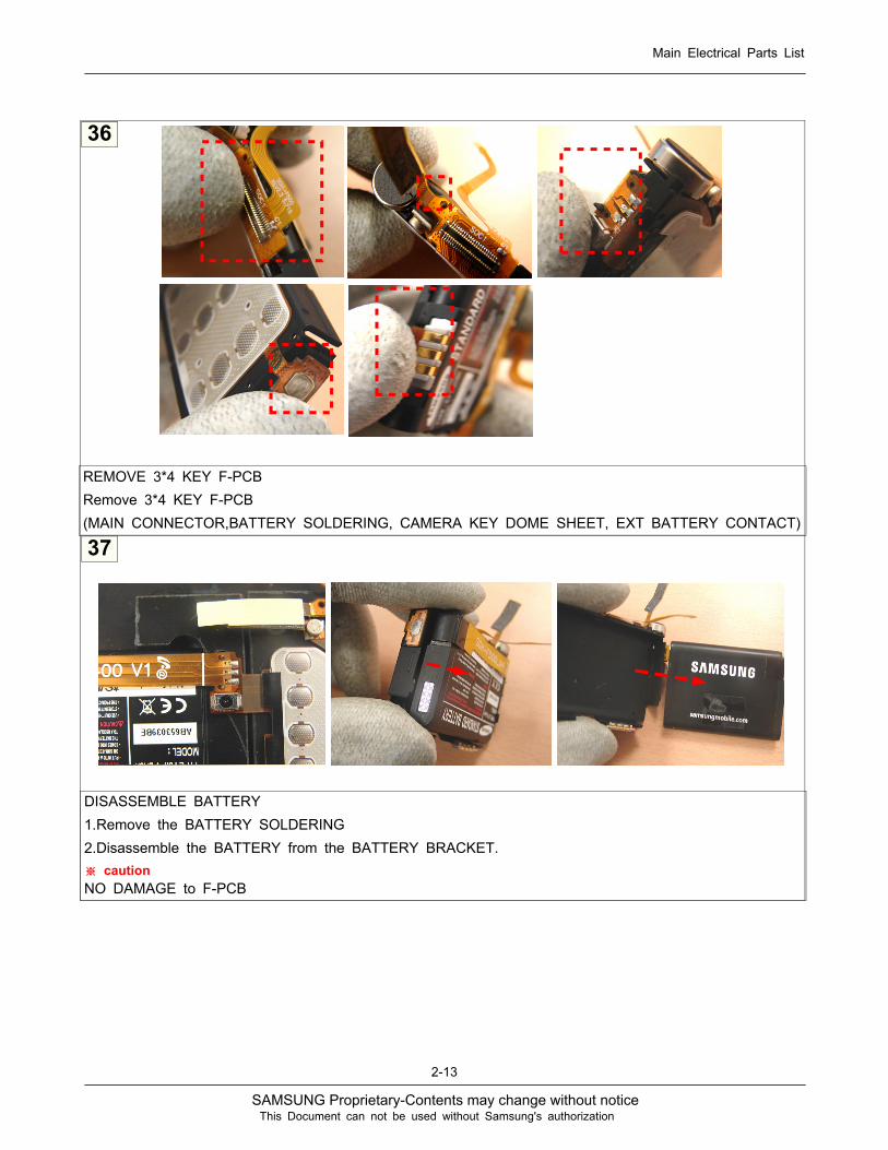
36
REMOVE 3*4 KEY F-PCBRemove 3*4 KEY F-PCB(MAIN CONNECTOR,BATTERY SOLDERING, CAMERA KEY DOME SHEET, EXT BATTERY CONTACT)
37
DISASSEMBLE BATTERY1.Remove the BATTERY SOLDERING2.Disassemble the BATTERY from the BATTERY BRACKET.※ cautionNO DAMAGE to F-PCB

SAMSUNG Proprietary-Contents may change without notice
Main Electrical Parts List
2-14
This Document can not be used without Samsung's authorization
38
1) REMOVE MOTORDisassemble the MOTOR from the 3*4 KEY PCBafter removing SOLDERING.2) Be careful not to damage the CON TO CON .

SAMSUNG Proprietary-Contents may change without notice
Main Electrical Parts List
2-15
This Document can not be used without Samsung's authorization
1
3
2
ATTACH 3*4 KEY 11. Prepare BATTERY BRACKET 2. Remove the 3*4 KEY's exfoliative sheet3. Attach the 3*4 KEY and Overlap holes 4. Remove BATTERY' exfoliative sheet5. Combine the BATTERY to theBRACKET 6. BATTERY F-PCB arrangement
2-4. Assembly
1) MOTOR SOLDERINGSolder the MOTOR to the 3*4 KEY PCB.
※ cautionWhen soldering the MOTOR, 3*4 KEY's holes mustbe overlapped with MOTOR PIN's holes.
1) BATTERY SOLDERING3*4 KEY ASS'Y와 BATTERY를 SOLDERING한다.Solder the 3*4 KEY ASS'Y to the BATTERY.
※ cautionIn the unlikely event of SHORT, It may be difficultto supply the right power.
①
⑥⑤④
③②

SAMSUNG Proprietary-Contents may change without notice
Main Electrical Parts List
2-16
This Document can not be used without Samsung's authorization
4
ATTACH 3*4 KEY 21.Attach MAIN CONNECTOR on BRACKET 2.Be careful of PIN Hole when attaching MAINCONNECTOR
3.attach BATTERY CONTACT 4.attach CAMERA KEY PART5.attach External BATTERY CONTACT 6.confirm final state
5 6
1) Join CON TO CON F-PCBJoin CON TO CON F-PCB and MAIN CONNETORas picture
①
⑥⑤④
③②
1) Attach ESD reinforcement F-PCB attachF-PCB on CONNECTOR
※ cautionBe careful of interference MIC when attachingF-PCB

SAMSUNG Proprietary-Contents may change without notice
Main Electrical Parts List
2-17
This Document can not be used without Samsung's authorization
1) Location of BATTERY BRACKT (Step 2)Push Battery Bracket to the upper direction like thedirection in the picture.
※ caution1) Be careful not to make scratch and molding
damage!2) Be careful not to damage the locker.
7 8
1) Location of BATTERY BRACKT (Step 1)Put Battery Bracket on the Swing Lower.
※ cautionWhen putting, inset Touch Key F-PCB through thehole first.
9 10
1) Assembly of CON TO CON F-PCB(Step 1)Push CON TO CON F-PCB in the inside of HINGE
※ cautionBe careful of FPCB cutting.
1) Assembly of CON TO CON F-PCB (Step 2)Look at the CON TO CON F-PCB after pushing
※ cautionNot allowed to be positioned on the downside ofHINGE

SAMSUNG Proprietary-Contents may change without notice
Main Electrical Parts List
2-18
This Document can not be used without Samsung's authorization
1) Assembly of MIC HOLDERPut MIC HOLDER on the MIC.
11 12
1) Assembly of SWING SIDE BELTInsert SWING SIDE BELT into LOWER.
13 14
1) Assembly of SWING UPPERPut SWING UPPER on the LOWER.
1)Attachment of TOUCH KEY F-PCBAttach TOUCH KEY F-PCB following silk line onthe TOUCH KEY PAD.

SAMSUNG Proprietary-Contents may change without notice
Main Electrical Parts List
2-19
This Document can not be used without Samsung's authorization
15
Assembly of TOUCH KEY1 ~ 2. Openning TOUCH KEY CONNECTOR, insert F-PCB to the SILK LINE.3. Shut the CONNECTOR after inserting F-PCB.4. Attach TOUCH KEY PAD on the SWING LOWER at last.
16 17
1) Assembly of SWING SCREW.Assemble the three point of screw following thedirection.
1) Attaching the LABELAttach the LABEL on the top of SWING assembly.
①
④③
②
SAMSUNG Proprietary-Contents may change without notice
Main Electrical Parts List
2-20
This Document can not be used without Samsung's authorization
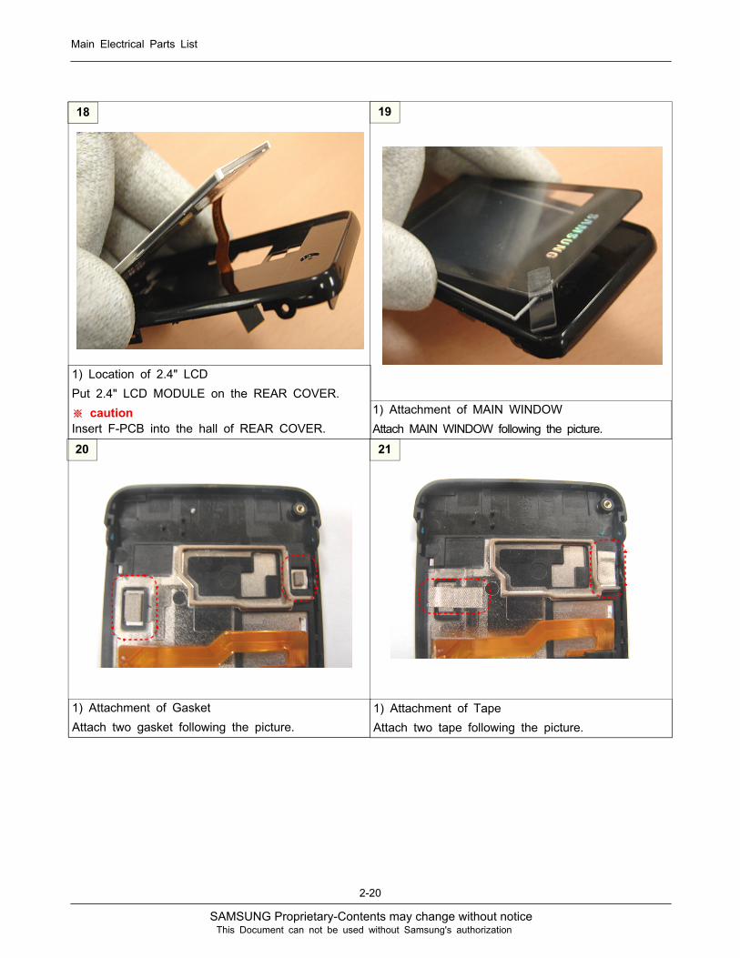
1) Attachment of MAIN WINDOWAttach MAIN WINDOW following the picture.
18 19
1) Location of 2.4" LCDPut 2.4" LCD MODULE on the REAR COVER.
※ cautionInsert F-PCB into the hall of REAR COVER.
20 21
1) Attachment of GasketAttach two gasket following the picture.
1) Attachment of TapeAttach two tape following the picture.

SAMSUNG Proprietary-Contents may change without notice
Main Electrical Parts List
2-21
This Document can not be used without Samsung's authorization
1) Attachment of 1.5" LCDRemoving the vinyl on the back of 1.5" LCD MODULE,attach the module on the SHIELD COVER.
22 23
1) Assembly of INTENNAPositioning the Intenna on the REAR COVER,tighten the SCREW.
24 25
1) Attachment of SUB WINDOWAttach the SUB WINDOW on the front cover.
1) Location of NAVI KEYLocate NAVI KEY on the FRONT COVER.
※ cautionLocating the NAVI KEY, watch the twelve of RIB.
SAMSUNG Proprietary-Contents may change without notice
Main Electrical Parts List
2-22
This Document can not be used without Samsung's authorization
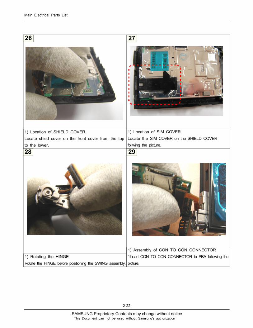
1) Location of SIM COVERLocate the SIM COVER on the SHIELD COVERfollwing the picture.
26 27
1) Location of SHIELD COVER.Locate shied cover on the front cover from the topto the lower.
28 29
1) Rotating the HINGERotate the HINGE before positioning the SWING assembly.
1) Assembly of CON TO CON CONNECTOR1Insert CON TO CON CONNECTOR to PBA following thepicture.

SAMSUNG Proprietary-Contents may change without notice
Main Electrical Parts List
2-23
This Document can not be used without Samsung's authorization
1) Location of PBALocate the PBA by the hook of FRONT COVER.
30 31
1) Assembly of HINGEAfter locating the PBA, locate the SWING HINGEon the FRONT COVER.
32 33
1) Arrangement of SWING on the FRONT COVERArrange the SWING PART on the FRONT COVER.
1) Arrangement of SWING on the FRONT COVERArrange PBA on the FRONT COVER.
SAMSUNG Proprietary-Contents may change without notice
Main Electrical Parts List
2-24
This Document can not be used without Samsung's authorization
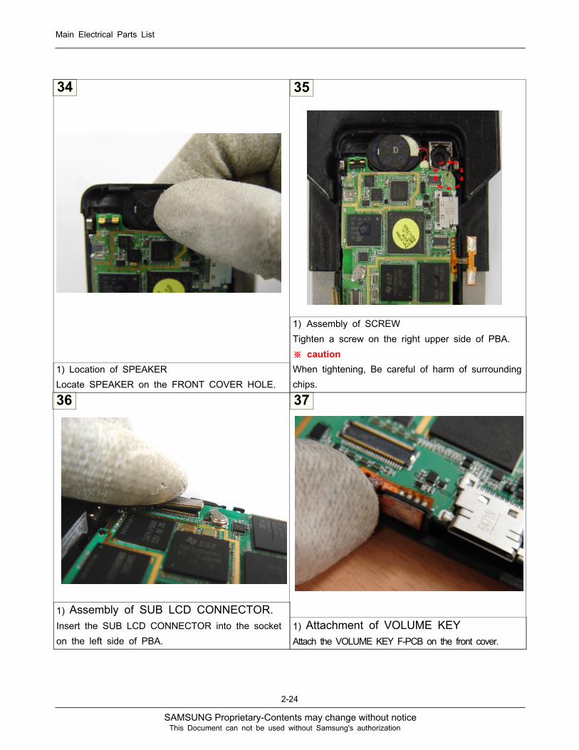
1) Assembly of SCREWTighten a screw on the right upper side of PBA.
※ cautionWhen tightening, Be careful of harm of surroundingchips.
34 35
1) Location of SPEAKERLocate SPEAKER on the FRONT COVER HOLE.
36 37
1) Assembly of SUB LCD CONNECTOR.Insert the SUB LCD CONNECTOR into the socketon the left side of PBA.
1) Attachment of VOLUME KEYAttach the VOLUME KEY F-PCB on the front cover.
SAMSUNG Proprietary-Contents may change without notice
Main Electrical Parts List
2-25
This Document can not be used without Samsung's authorization
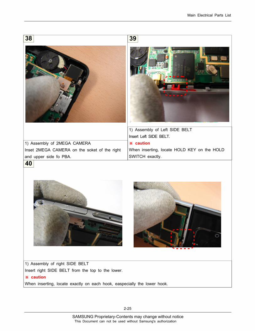
1) Assembly of Left SIDE BELTInsert Left SIDE BELT.
※ cautionWhen inserting, locate HOLD KEY on the HOLDSWITCH exactly.
38 39
1) Assembly of 2MEGA CAMERAInset 2MEGA CAMERA on the soket of the rightand upper side fo PBA.
40
1) Assembly of right SIDE BELTInsert right SIDE BELT from the top to the lower.
※ cautionWhen inserting, locate exactly on each hook, easpecially the lower hook.
SAMSUNG Proprietary-Contents may change without notice
Main Electrical Parts List
2-26
This Document can not be used without Samsung's authorization
1) Assembly of REAR partAssembe the rear part follwing the picture.
※ cautionAssembe the locker from the upper to the lower,one by one.
41 42
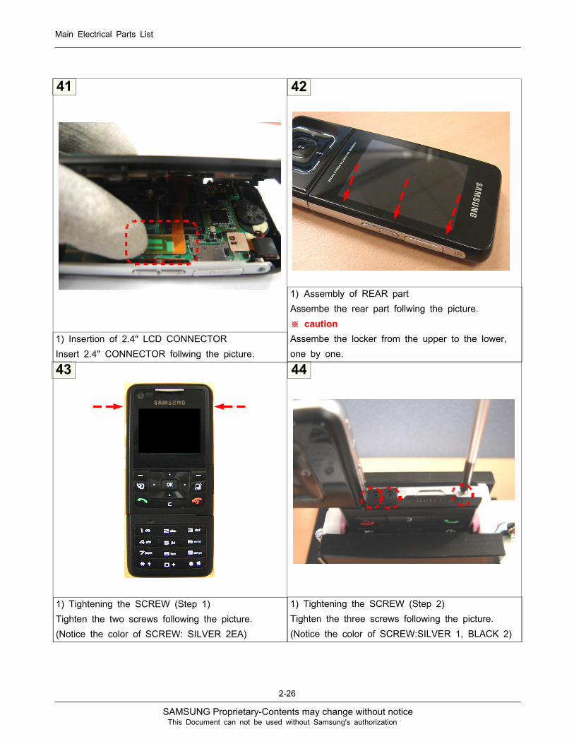
1) Insertion of 2.4" LCD CONNECTORInsert 2.4" CONNECTOR follwing the picture.
43 44
1) Tightening the SCREW (Step 1)Tighten the two screws following the picture.(Notice the color of SCREW: SILVER 2EA)
1) Tightening the SCREW (Step 2)Tighten the three screws following the picture.(Notice the color of SCREW:SILVER 1, BLACK 2)
SAMSUNG Proprietary-Contents may change without notice
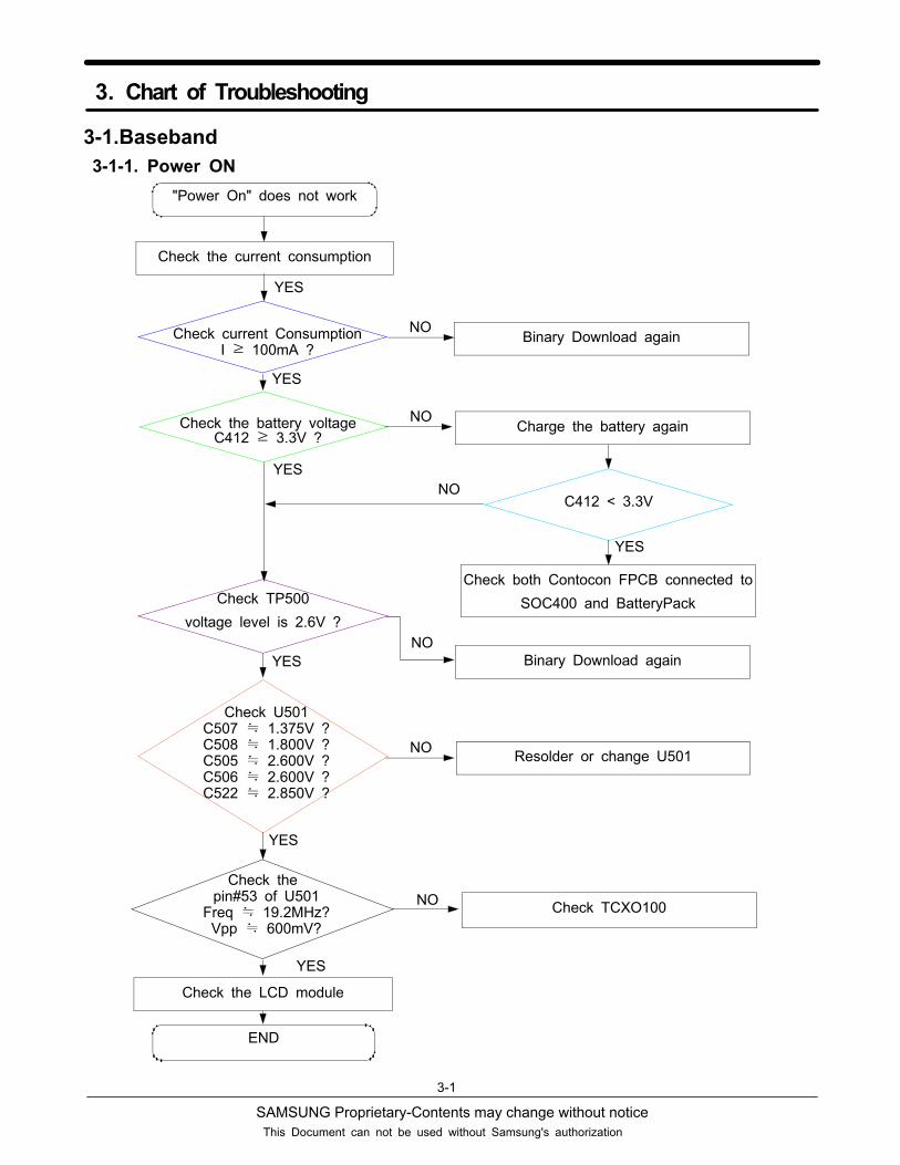
3-1
This Document can not be used without Samsung's authorization
3. Chart of Troubleshooting
3-1.Baseband3-1-1. Power ON
Check TP500voltage level is 2.6V ?
Check U501C507 ≒ 1.375V ?C508 ≒ 1.800V ?C505 ≒ 2.600V ?C506 ≒ 2.600V ?C522 ≒ 2.850V ?
Check thepin#53 of U501
Freq ≒ 19.2MHz?Vpp ≒ 600mV?
Check the LCD module
END
Binary Download again
Resolder or change U501
Check TCXO100
YES
YES
YES
NO
NO
NO
"Power On" does not work
Check the current consumption
Check current ConsumptionI ≥ 100mA ?
Check the battery voltageC412 ≥ 3.3V ?
Binary Download again
Charge the battery again
Check both Contocon FPCB connected toSOC400 and BatteryPack
YES
YES
YES
NO
NO
C412 < 3.3V
YES
NO

SAMSUNG Proprietary-Contents may change without notice
Flow Chart of Troubleshooting and Circuit Diagrams
3-2
This Document can not be used without Samsung's authorization
C15110nF6.3V
R119
C1521.5NF
V01
100
V_2.85TCXO
KT3225R19200DCV28LEATCXO100GND
2
3
OUTVCC
4
1VCON
6.3V100nFC146
TRK_LO_ADJ
TCXO
C423
314C
214C
004D
VBAT
SAMSUNG Proprietary-Contents may change without notice
Flow Chart of Troubleshooting and Circuit Diagrams
3-3
This Document can not be used without Samsung's authorization
V_2
.85R
X
R50
2
VRE
G_U
SB
10
VRE
G_W
LAN
64
VSW
_5V
14
VSW
_MSM
C31
VSW
_MSM
E37
VSW
_PA
27
XTA
L_IN
44X
TAL_
OU
T46
VRE
G_M
SMP
50
VR
EG
_PA
28
VRE
G_R
FRX1
69VR
EG
_RFR
X267
VREG
_RFT
X73
VR
EG_R
UIM
42
VREG
_SY
NT
81V
RE
G_T
CX
O84
VDD
_RU
IM
VD
D_S
PKR
77
VD
D_W
LAN
6525V
IB_D
RV_
N
VREG
_5V
12 39VR
EG
_MM
C
VR
EG
_MS
MA
56
VR
EG
_MS
MC
32
VRE
G_M
SME
3660
54V
DD
_AN
A
VDD
_MAI
N83
VDD
_MS
M5233
VD
D_M
SMC
VD
D_M
SME
35
VD
D_P
A29 71
VD
D_R
F
41
USB
_DA
T17
USB
_D_M
2018U
SB_D
_PU
SB_I
D1113
USB
_OE
_N
19U
SB_S
E0
USB
_VBU
S16
VBA
CKU
P48
VBA
T6
VC
HG
2
VC
OIN
SPK
R_B
YP7478
SPK
R_I
N_M
SPKR
_IN
_P76 79
SPK
R_O
UT_
MSP
KR_O
UT_
P75
TCXO
_EN
55TC
XO_I
N58
TCXO
_OU
T53
USB
_CTL
_N15 80 38
RU
IM_C
LK
26R
UIM
_IO
RU
IM_M
_CLK
34
RU
IM_M
_IO
30
RU
IM_M
_RST
40 43R
UIM
_RS
T
49S
BCK
SBD
T47
SBS
T51
SLE
EP_C
LK45
LCD
_DR
V_N
59M
SM
_IN
T_N
CN68
CN78
9P
ON
_RE
SET_
N
PS_
HO
LD57
RE
F_BY
P63
REF
_GN
D62
REF
_ISE
T61
REF
_OU
T
CBL
1PW
R_N
CH
G_C
TL_N
4
8FL
SH
_DR
V_N
DNG58
GP
1_D
RV_
N21
ISN
S_M
5IS
NS
_P3 24
KPD
PW
R_N
KPD
_DR
V_N
2322
AD
C_B
YP
1
AM
UX_
IN1
70A
MU
X_IN
272
AM
UX_
OU
T82
BAT
_FET
_N7
CBL
0PW
R_N
6866
L501
V_M
IC_2
.85V
U50
1
C51
1
C51
4
TP50
0
V_1.
375C
C52
0
C50
9
C53
7C
528
C51
8
C50
3
C50
5
TP50
1
V_2
.85R
X1
C52
1
L500
C53
8C
530
C52
3
3 2
R50
3
Q50
01
C50
6
C50
2
C50
4
V_2.
6P
C52
4
005 R
OS
C50
0
C51
9
C50
8
C51
3C
512
C51
0
V05
C51
6
V_2
.85U
SIM
R50
4
C52
9
C50
0
BAT5
00
SOP GEN
C52
5C
522
C52
7
V_2
.85T
X
VBA
T
V_1.
8E
C51
7
V_B
T_3.
05V
VBA
T
C50
1
C53
6C
535
V_2.
85TC
XO
V_2.
85O
SC
V_2
.6A
R50
1
C51
5
C50
7
C52
6
PS_
HO
LD
EXT_
BAT_
ADC
INN
ER
_BA
T_AD
C
USB
_VC
C
JIG
_ON
US
IM_R
ESE
T
PM_S
BC
KPM
_SB
DT
PM
_SBS
T
TCXO
_EN
US
B_VP
O
MSM
_D-
MSM
_D+
USB
_OE_
N
USB
_VM
O
TCXO
TCX
O_O
UT
SLE
EP_X
TAL_
IN
AMU
X_O
UT
ON
_SW
PM
_IN
T_N
RES
ET_I
N
PMIC
3_R
EF
USI
M_C
LK
US
IM_D
ATA
USI
M_M
_CLK
US
IM_M
_DAT
A
US
IM_M
_RES
ET
SAMSUNG Proprietary-Contents may change without notice
Flow Chart of Troubleshooting and Circuit Diagrams
3-4
This Document can not be used without Samsung's authorization

SAMSUNG Proprietary-Contents may change without notice
Flow Chart of Troubleshooting and Circuit Diagrams
3-5
This Document can not be used without Samsung's authorization
SAMSUNG Proprietary-Contents may change without notice
Flow Chart of Troubleshooting and Circuit Diagrams
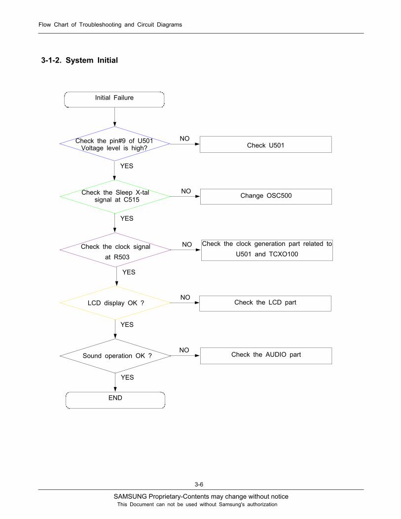
3-6
This Document can not be used without Samsung's authorization
3-1-2. System Initial
Initial Failure
Check the pin#9 of U501Voltage level is high?
LCD display OK ?
END
Check U501
Check the Sleep X-talsignal at C515
YES
Check the clock signalat R503
YES
YES
YES
YES
Sound operation OK ?
NO
Change OSC500NO
Check the clock generation part related toU501 and TCXO100
NO
Check the LCD partNO
Check the AUDIO partNO

SAMSUNG Proprietary-Contents may change without notice
Flow Chart of Troubleshooting and Circuit Diagrams
3-7
This Document can not be used without Samsung's authorization

SAMSUNG Proprietary-Contents may change without notice
Flow Chart of Troubleshooting and Circuit Diagrams
3-8
This Document can not be used without Samsung's authorization
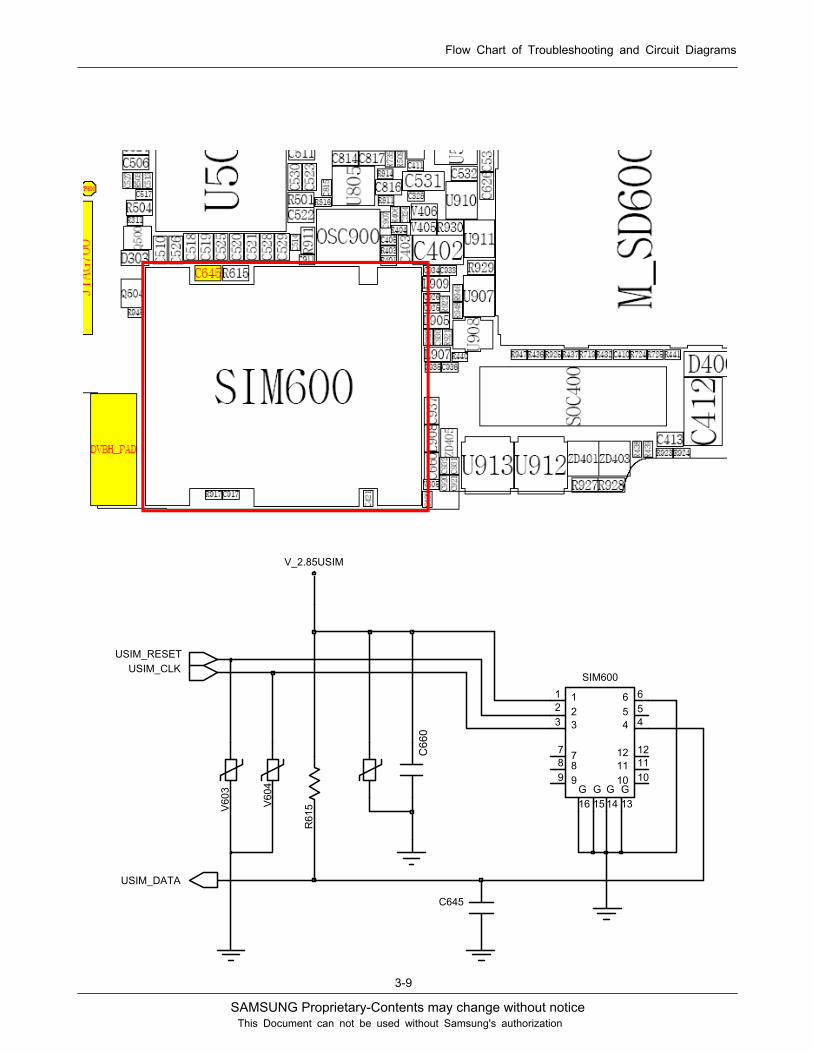
3-1-3. SIM Part
"Please insert SIM card"
END
Check the voltageat SIM600
pin#1 = 2.85V ?
Check the SIM600connect to SIM card
socket
YES
YES
Resolder or change SIM600NO
Change the SIM600
check SIM600 and UCP300
NO
Check the SIM card
There is any signalpin#2, #3, #4 of SIM600
NO
YES
SAMSUNG Proprietary-Contents may change without notice
Flow Chart of Troubleshooting and Circuit Diagrams
3-9
This Document can not be used without Samsung's authorization
V_2.85USIM
306V
066C
406V
8 899
G1314
GG1516
G
11 111212
223 3 4 4
556 6
77
SIM6001 1
1010
516R
C645
USIM_CLK
USIM_DATA
USIM_RESET

SAMSUNG Proprietary-Contents may change without notice
Flow Chart of Troubleshooting and Circuit Diagrams
3-10
This Document can not be used without Samsung's authorization
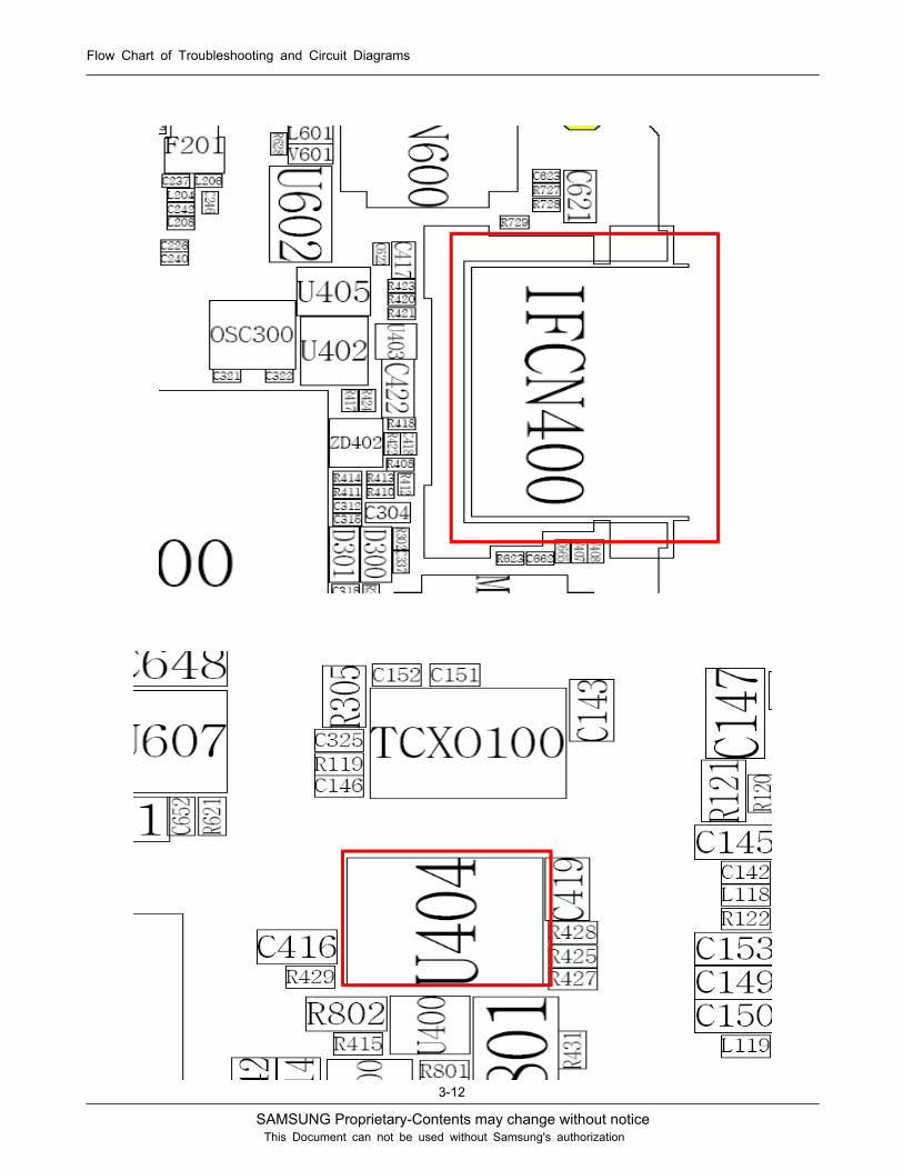
3-1-4. Charging Part
Charging does not work
END
Check IFCN400 connection statuswith TA
NO
Check U404 pin#3 = LOW Change U404NO
If charging with TA,check voltage level
at U404 pin#1 = 5V
YES
If charging with USB,check voltage level
at U404 pin#2 = 5V
NO Check IFCN400 connection statuswith USB
YES
YES

SAMSUNG Proprietary-Contents may change without notice
Flow Chart of Troubleshooting and Circuit Diagrams
3-11
This Document can not be used without Samsung's authorization
724R
914C
924R
244R
R425
824R
VBAT
ICDL
6IMIN
USB2
USBON 7_CHG4
_EN5
3 _PPR
U404
BAT 10CRDL
1
11GND
GND 8
9TA_VEXT
CHG_ON
CHRG_COMPLETE USB_VCC
ICHRGUSB_VCC
CHG_DET
7 78
89 9
21 NCNC22NC23
24 NC
1819 19
22
2020
33
445 5
66
1011 11
1212
1313
141415 15
161617 17
18
IFCN4001 1
10
R417
C401
V400
R413
VBAT
V403
R402
V402
R412
C408
V_MIC_2.85V
V401
614C
C400
204DZ
1 2 3456
7 8
R408
R405
R418
604C
C409
R411
V_2.6P
R407
R410
C422
R414
R415
C407
R400
C404
KC
OLC
6
DN
G2
OI1
CN
5
3MI
SC
CV
4
204U
EAR_SW
D-
USB_VCC
IF2
TXD_T
MIC2N
EAR_R
EAR_L
TA_VEXT
BOOT_SWJACK_IN
JIG_ON_IFRXD_1
D+
JIG_ON_IF_T
RXD_T
MIC2P
SAMSUNG Proprietary-Contents may change without notice
Flow Chart of Troubleshooting and Circuit Diagrams
3-12
This Document can not be used without Samsung's authorization

SAMSUNG Proprietary-Contents may change without notice
Flow Chart of Troubleshooting and Circuit Diagrams
3-13
This Document can not be used without Samsung's authorization
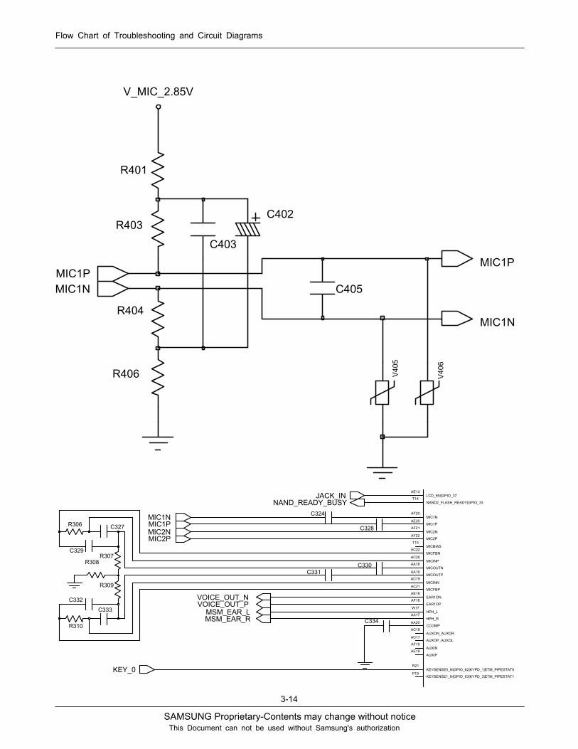
3-1-5. Microphone Part
Microphone does not work
END
Reassemble MicrophoneNO
MIC filter circuit aroundUCP300 is OK ?
Resolder MIC filter circuit or checkUCP300
NO
NO Check the MIC bias circuit path
YES
YES
Is the assembled status ofMicropohone OK ?
Check the DC bias voltageon MIC path C405 = 2.3V ?
YES
SAMSUNG Proprietary-Contents may change without notice
Flow Chart of Troubleshooting and Circuit Diagrams
3-14
This Document can not be used without Samsung's authorization
504V
R404
R401
C403
R406
R403
C405
604V
C402
V_MIC_2.85V
MIC1N
MIC1N
MIC1PMIC1P
R310
R307
R306
R309
HPH_LW17
NAND2_FLASH_READY|GPIO_33T14
MICBIAST15
R21KEYSENSE0_N|GPIO_62|KYPD_1|ETM_PIPESTAT0
P19KEYSENSE1_N|GPIO_63|KYPD_3|ETM_PIPESTAT1
AF20
MIC2NAF21
MIC2PAF22
EAR1OPAF18
AUXINAF19
MIC1N
EAR1ONAE18
AUXIPAE19
MIC1PAE20
LCD_EN|GPIO_37AE13
AC19
MICINPAC20
MICFBPAC21
MICFBNAC22
AUXOP_AUXOLAC17
AUXON_AUXORAC18
MICINN
HPH_RAA17
MICOUTNAA18
MICOUTPAA19
CCOMPAA20
C331
C334
C333
C328
C324
C329
C332
C327
R308 C330
MIC2N
NAND_READY_BUSYJACK_IN
MSM_EAR_R
MIC2P
VOICE_OUT_N
MSM_EAR_LVOICE_OUT_P
MIC1PMIC1N
KEY_0

SAMSUNG Proprietary-Contents may change without notice
Flow Chart of Troubleshooting and Circuit Diagrams
3-15
This Document can not be used without Samsung's authorization
SAMSUNG Proprietary-Contents may change without notice
Flow Chart of Troubleshooting and Circuit Diagrams
3-16
This Document can not be used without Samsung's authorization
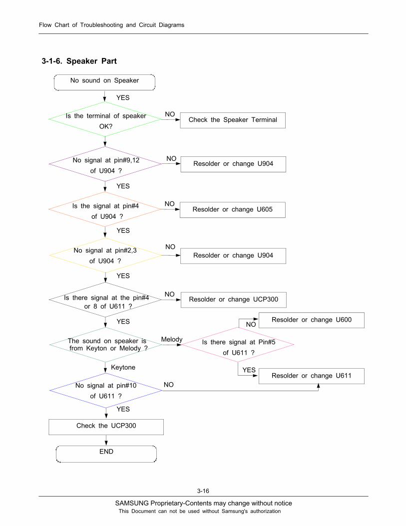
3-1-6. Speaker Part
No sound on Speaker
END
Check the Speaker TerminalNO
Is the signal at pin#4of U904 ?
YES
Is the terminal of speakerOK?
No signal at pin#9,12of U904 ?
Check the UCP300
No signal at pin#10of U611 ?
No signal at pin#2,3of U904 ?
Is there signal at the pin#4or 8 of U611 ?
The sound on speaker isfrom Keyton or Melody ?
YES
YES
YES
YES
Keytone
YES
Resolder or change U904NO
Resolder or change U605NO
Resolder or change U904NO
Resolder or change UCP300NO
Melody Is there signal at Pin#5of U611 ?
Resolder or change U600
Resolder or change U611
NO
YES
NO

SAMSUNG Proprietary-Contents may change without notice
Flow Chart of Troubleshooting and Circuit Diagrams
3-17
This Document can not be used without Samsung's authorization

SAMSUNG Proprietary-Contents may change without notice
Flow Chart of Troubleshooting and Circuit Diagrams
3-18
This Document can not be used without Samsung's authorization
C624
826R
016R
C659
VBAT
R606
R604
VOM
9VOP
1VREF
5
SSV
SSV
6
VSS 11
VSS 10
7 8
DD
V
DD
V
13
DDV
1415
DDV
16
DDV
VIM2
VIP3
12
4EN
17
DN
GNC1819 NC
DD
V
U904
726C
926R
C 6
GND2 VCC 5
4Y
U6051 A
B3
926C
R605
C628
C630
DM_2.9V
116R
SPK_RCV_N
AMP_L
SPK_RCV_P
MSM_AMP_EN
DM_AMP_EN
906R
DM_2.9V
3GND
1NI
8
2NI
4
1C
N
10
7NC2
NO12
52
ON
VCC9
U611COM1
1
COM2 6
C631
736C
436C
806R
R_R
AE_M
SM
L_R
AE_M
SM
EAR_AMP_R
2NE_
WS_
DU
A
AK_SPK_L
AMP_L
R_KP
S_K
A

SAMSUNG Proprietary-Contents may change without notice
Flow Chart of Troubleshooting and Circuit Diagrams
3-19
This Document can not be used without Samsung's authorization
DM_2.9V
C611
C601
C607C60633NF
L600
C613
C617
206C
C608
C618
C612
C616
C604K9MIC2_OUT
K10NC
K2 RXN_IN
K3RXP_IN
K4HF_IN
K5 TXP_OUT
K6AVSS
K7AGNDK8
AGNDOUT
J3MEL_R
J4MEL_L
J5TXN_OUT
J6AVDD
J7MICBIAS2
J8MICBIAS1
J9MIC2P_IN
K1NC
G9MIC1_OUT
H1SPR_OUT
H10MIC1P_IN
H2SPL_OUT
H9 MIC1N_IN
J1 RXR_IN
J10MIC2N_IN
J2RXL_IN
E9RVSS
F1MSTCLK_I
F10MUTEC
F2NRST
F9HF_OUT
G1TEST
G10AIN1
G2PLLC2
C9EPL_OUT
D1DVSS_I
D10RCVP_OUT
D2DVDD_I
D9 RCVN_OUT
E1SDA
E10RVDD
E2SCL
B6BCLK1
B7 LRCLK1
B8SDTI0
B9PLLC1
C1MSTCLK_O
C10EPR_OUT
C2AUXCLK
C3NC
A8BCLK0
A9 LRCLK0
B1DVDD_C
B10PLLC3
B2DVDD_D
B3PCMCLK
B4DCLK
B5 MCLK1A1
NCA10NC
A2DVSS_C
A3PCMIN
A4FSYNC A5
PCMOUT
A6SDTI1
A7 MCLK0
AK2443
U600
1NC 2NC
C609
C605
C600
C610
PCM_DOUT
MIC2N
MIC2P
AK_SPK_R
A_BCKA_MSCK
AK_SPK_L
AK_BT_LAK_BT_R
PCM_DCLKPCM_FCLKPCM_DIN
MIC1P
AK_RESET
A_LRCKA_SDOUT
PCM_CLK
AP_SDAAP_SCL
AK_MCLK
MIC1N

SAMSUNG Proprietary-Contents may change without notice
Flow Chart of Troubleshooting and Circuit Diagrams
3-20
This Document can not be used without Samsung's authorization
3-1-7. Receiver Part
No sound on Receiver
END
Check the Receiver TerminalNO
YES
Is the terminal of receiverOK?
YES
YES
No signal at pin#1,6of U606 ?
Resolder or change U606NO
Is the signal at R626of U606 ?
YES
YES
Resolder or change UCP300NO
No signal at pin#2,5of U606 ?
Resolder or change U606NO
Is there signal at R607,R613, C657, C658 ?
Resolder or change UCP300NO

SAMSUNG Proprietary-Contents may change without notice
Flow Chart of Troubleshooting and Circuit Diagrams
3-21
This Document can not be used without Samsung's authorization
C657
C658
626RVBAT
R607
R613
6
3GND
1NI
8
2NI
4
1C
N
10
7NC2
NO12
52
ON
VCC9
U606
COM11
COM2
SPK_RCV_N
SPK_RCV_P
NE_W
S_D
UA
VOICE_OUT_P
VOICE_OUT_N
SAMSUNG Proprietary-Contents may change without notice
Flow Chart of Troubleshooting and Circuit Diagrams
3-22
This Document can not be used without Samsung's authorization
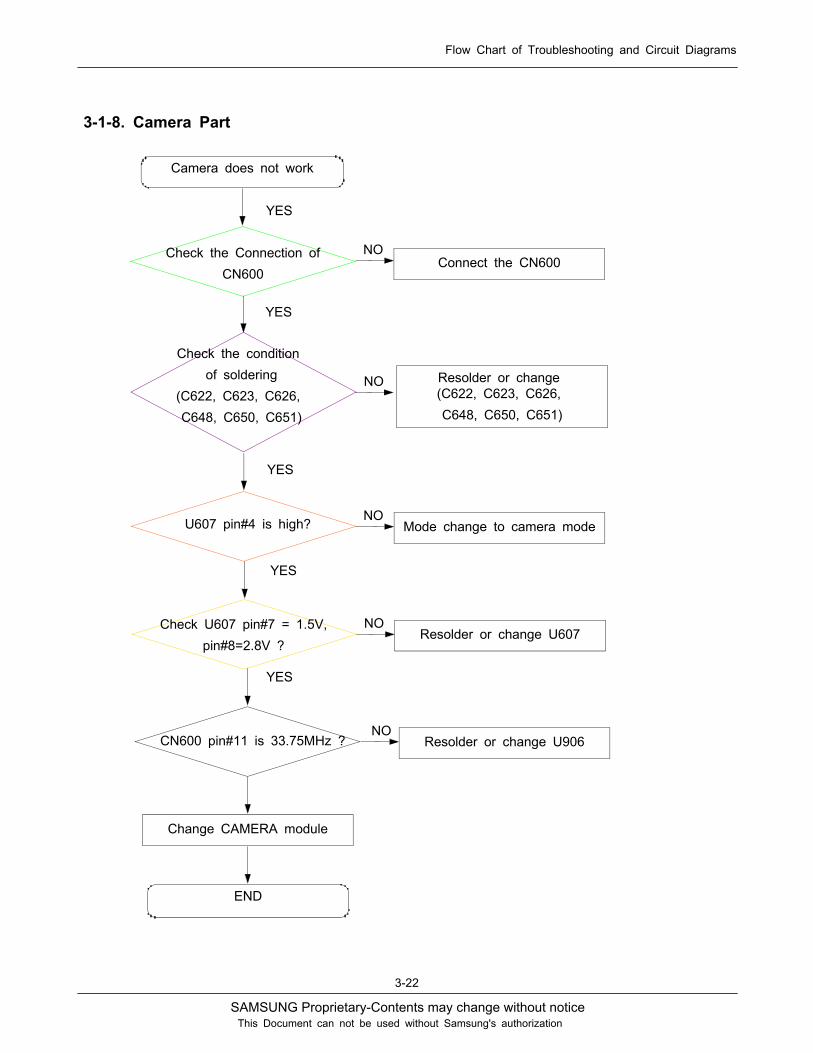
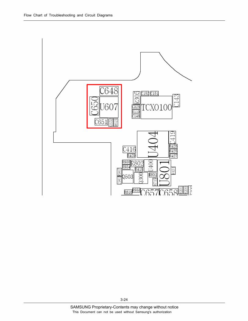
3-1-8. Camera Part
Camera does not work
END
Connect the CN600NO
YES
Check the Connection ofCN600
YES
YES
Check the conditionof soldering
(C622, C623, C626,C648, C650, C651)
Resolder or change(C622, C623, C626,C648, C650, C651)
NO
U607 pin#4 is high?
YES
YES
Mode change to camera modeNO
Check U607 pin#7 = 1.5V,pin#8=2.8V ?
Resolder or change U607NO
CN600 pin#11 is 33.75MHz ? Resolder or change U906NO
Change CAMERA module

SAMSUNG Proprietary-Contents may change without notice
Flow Chart of Troubleshooting and Circuit Diagrams
3-23
This Document can not be used without Samsung's authorization
SAMSUNG Proprietary-Contents may change without notice
Flow Chart of Troubleshooting and Circuit Diagrams
3-24
This Document can not be used without Samsung's authorization

SAMSUNG Proprietary-Contents may change without notice
Flow Chart of Troubleshooting and Circuit Diagrams
3-25
This Document can not be used without Samsung's authorization
326C
6
VCAM_1.5VVCAM_2.8V
5 56 67 78 89
9
12C
NC
N22
17 1718 1819 19
2 2
20 20
3 34 41 1
10 1011 1112 1213 1314 1415 1516 16
CN600
226C
26C
CAM_RESET-
CAM_DAT(3)_S
AP_SDA
CAM_PCLK
CAM_MCLK
CAM_DAT(6)_S
CAM_DAT(4)_S
CAM_VSYNC
CAM_HSYNC
AP_SCL
CAM_DAT(2)_SCAM_DAT(1)_S
CAM_DAT(5)_SCAM_DAT(0)_S
CAM_DAT(7)_S
2
DN
G
9
NC 6
1 VIN 8VOUT1
VOUT2 7
C652
U607
BYP3
5EN14 EN2
GND
VBAT
C651
VCAM_1.5V
VCAM_2.8V
126R
C650
C648
CAM_EN
NE_M
AC
SAMSUNG Proprietary-Contents may change without notice
Flow Chart of Troubleshooting and Circuit Diagrams
3-26
This Document can not be used without Samsung's authorization
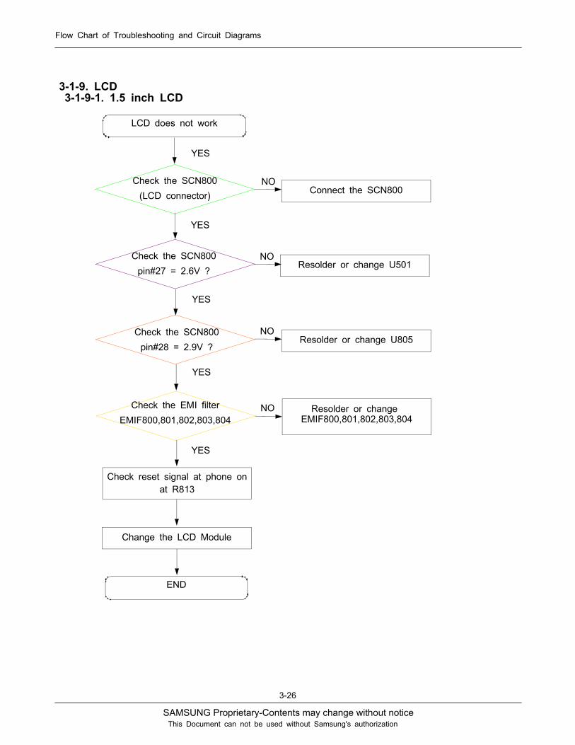
3-1-9. LCD3-1-9-1. 1.5 inch LCD
LCD does not work
END
Connect the SCN800NO
YES
Check the SCN800(LCD connector)
YES
YES
Check the SCN800pin#27 = 2.6V ?
NO
YES
YES
Resolder or change U805NO
Check the EMI filterEMIF800,801,802,803,804
Resolder or changeEMIF800,801,802,803,804
NO
Change the LCD Module
Check the SCN800pin#28 = 2.9V ?
Resolder or change U501
Check reset signal at phone onat R813

SAMSUNG Proprietary-Contents may change without notice
Flow Chart of Troubleshooting and Circuit Diagrams
3-27
This Document can not be used without Samsung's authorization
3-1-9-2. 2.4 inch LCD
LCD does not work
Connect the MCN600NO
YES
Check the CN900(LCD connector)
YES
Check the CN900pin#8 = 2.9V ?
YES
END
YES
Check the EMI filterEMIF600, 601, 602
F901, 902, 903, 904
Resolder or changeEMIF600, 601, 602
F901, 902, 903, 904
NO
Change the LCD Module
NO Resolder or change U805

SAMSUNG Proprietary-Contents may change without notice
Flow Chart of Troubleshooting and Circuit Diagrams
3-28
This Document can not be used without Samsung's authorization
DM_2.9V
R813
C823R817R818
545464
64
5 56 67788
9 9
3939
44
404041414242
43 4344 44
3131323233 3334 34
3535363637 3738 38
242425 2526 26
2727282829 29
33
30 30
161617 1718 18
1919
2 2
202021 2122 22
2323
SCN800
1 1
10 1011111212
13 1314 141515
KEY_3.3V V_2.6P VBAT
R820R819
RESET_OUT
LCD_FLM
LED2LED+
ELCD_RS
SCAN_0SCAN_1SCAN_2
KEY_0KEY_1KEY_2KEY_3
ELCD_CSELCD_WE
LED1LED3
ELCD_D(0)ELCD_D(2)ELCD_D(4)ELCD_D(6)ELCD_D(8)
ELCD_D(10)ELCD_D(12)ELCD_D(14)
ELCD_RE
ELCD_D(3)ELCD_D(5)ELCD_D(7)ELCD_D(9)ELCD_D(11)ELCD_D(13)ELCD_D(15)
ELCD_D(1)
ON_SW
DM_2.9V
009C
99
G51 52
G
4647 47 48 4849 49
55
50 50
6677 88
39
44
40 4041 41 42 4243 43 44 4445 45 46
31 32 32
3333 34 34
3535 36 36
3737 383839
2425 25 2626
2727 28 28
2929
33
303031
17 18 18
1919
22
20 20
2121 22 22
2323 24
1
10 10
1111 12 121313 14 14
1515 16 16
17
CN900
1
U923
C662
MLCD_LED2MLCD_LED3MLCD_LED4MLCD_LED5
MLCD_FLM
MLCD_D(0) MLCD_SDO
MLCD_D(3)
MLCD_D(8)MLCD_D(9)
MLCD_D(10)MLCD_D(11)MLCD_D(12)MLCD_D(13)MLCD_D(14)MLCD_D(15)
MLCD_VOUT
MLCD_LED1
MLCD_D(1)
MLCD_D(7)MLCD_D(6)MLCD_D(5)MLCD_D(4)
MLCD_D(2)
IM1IM2
MLCD_RSLCD_RE
MLCD_VSYNCMLCD_HSYNC
MLCD_OE
MLCD_D1(4)
DMLCD_MCLK
MLCD_D1(3)
MLCD_D1(5)
MLCD_CS
LCD_RESET
MLCD_D1(2)MLCD_D1(1)MLCD_D1(0)
SCL_WE
SAMSUNG Proprietary-Contents may change without notice
Flow Chart of Troubleshooting and Circuit Diagrams
3-29
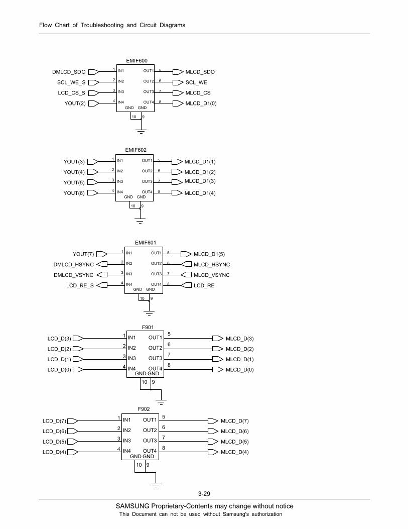
This Document can not be used without Samsung's authorization
2
3 IN3
IN44
5OUT1
OUT2 6
7OUT3
OUT4 8
EMIF600
9
GNDGND
10
1 IN1
IN2
6
7OUT3
OUT4 8
9
GNDGND
10
1 IN1
IN22
3 IN3
IN44
5OUT1
OUT2
3
4 IN4
OUT1 5
6OUT2
OUT3 7
8OUT4
EMIF602
EMIF601
GND
910
GND
IN11
2 IN2
IN3
LCD_CS_S
YOUT(6)
YOUT(5) MLCD_D1(3)
MLCD_D1(4)
YOUT(4) MLCD_D1(2)
YOUT(3) MLCD_D1(1)
YOUT(2) MLCD_D1(0)
SCL_WE_S SCL_WE
YOUT(7) MLCD_D1(5)
MLCD_CS
MLCD_VSYNC
DMLCD_HSYNC MLCD_HSYNC
DMLCD_SDO MLCD_SDO
LCD_RE_S LCD_RE
DMLCD_VSYNC
IN4
OUT1 5
6OUT2
OUT3 7
8OUT4
F902
GND910
GND
IN11
2 IN2
IN33
4
4 IN4
OUT15
6OUT2
OUT37
8OUT4
F901
GND910
GND
IN11
2 IN2
IN33
MLCD_D(5)
MLCD_D(4)
MLCD_D(3)
MLCD_D(2)
MLCD_D(1)
MLCD_D(0)
LCD_D(3)
MLCD_D(7)
MLCD_D(6)
LCD_D(7)
LCD_D(1)
LCD_D(0)
LCD_D(2)
LCD_D(4)
LCD_D(5)
LCD_D(6)
SAMSUNG Proprietary-Contents may change without notice
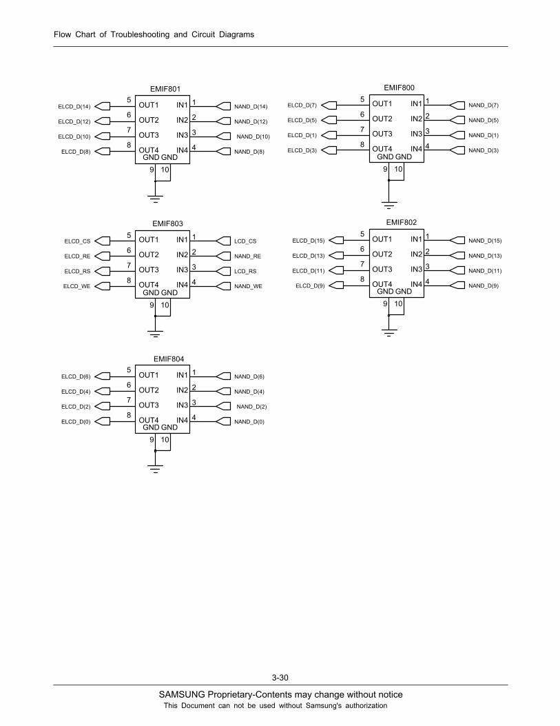
Flow Chart of Troubleshooting and Circuit Diagrams
3-30
This Document can not be used without Samsung's authorization
3IN3
IN4 4
5 OUT1
OUT26
7 OUT3
OUT48
EMIF803
9GND GND
10
1IN1
IN2 2
OUT48
GND10
1IN1
IN2 2
3IN3
IN4 4
5OUT1
OUT26
7OUT3
EMIF804
9GND
4
5OUT1
OUT26
7OUT3
OUT48
9GND GND
10
1IN1
IN2 2
3IN3
IN4
EMIF802
8
10
1IN1
IN2 2
3IN3
IN4 4
5OUT1
OUT26
7OUT3
OUT4
EMIF801
9GND GND
8
10
1IN1
IN2 2
3IN3
IN4 4
5 OUT1
OUT26
7 OUT3
OUT4
EMIF800
9GND GND
ELCD_D(14)
ELCD_D(12)
ELCD_D(8)
ELCD_D(10) ELCD_D(1)
ELCD_RS
ELCD_CS
ELCD_D(6)
ELCD_D(0)
ELCD_D(4)
NAND_D(7)
NAND_D(8)
NAND_D(12)
NAND_D(6)
NAND_D(4)
NAND_D(0)
NAND_D(2)ELCD_D(2)
NAND_D(15)
NAND_D(13)ELCD_D(13)
ELCD_D(15)
NAND_D(9)
NAND_D(11)
ELCD_D(9)
ELCD_D(11)
NAND_D(5)ELCD_D(5)
ELCD_D(7)
NAND_D(1)
NAND_D(3)ELCD_D(3)
LCD_RS
NAND_WEELCD_WE
LCD_CS
NAND_REELCD_RE
NAND_D(14)
NAND_D(10)

SAMSUNG Proprietary-Contents may change without notice
Flow Chart of Troubleshooting and Circuit Diagrams
3-31
This Document can not be used without Samsung's authorization
SAMSUNG Proprietary-Contents may change without notice
Flow Chart of Troubleshooting and Circuit Diagrams
3-32
This Document can not be used without Samsung's authorization
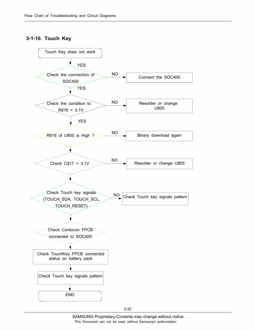
3-1-10. Touch Key
Touch Key does not work
Connect the SOC400NO
YES
Check the connection ofSOC400
YES
Check the condition toR816 = 3.1V
YES
END
R816 of U805 is High ? Binary download againNO
NO Resolder or changeU805
Check C817 = 3.1V
Check Touch key signals(TOUCH_SDA, TOUCH_SCL,
TOUCH_RESET)
Check Contocon FPCBconnected to SOC400
Resolder or change U805NO
Check Touch key signals patternNO
Check TouchKey FPCB connectedstatus on battery pack
Check Touch key signals pattern
SAMSUNG Proprietary-Contents may change without notice
Flow Chart of Troubleshooting and Circuit Diagrams
3-33
This Document can not be used without Samsung's authorization
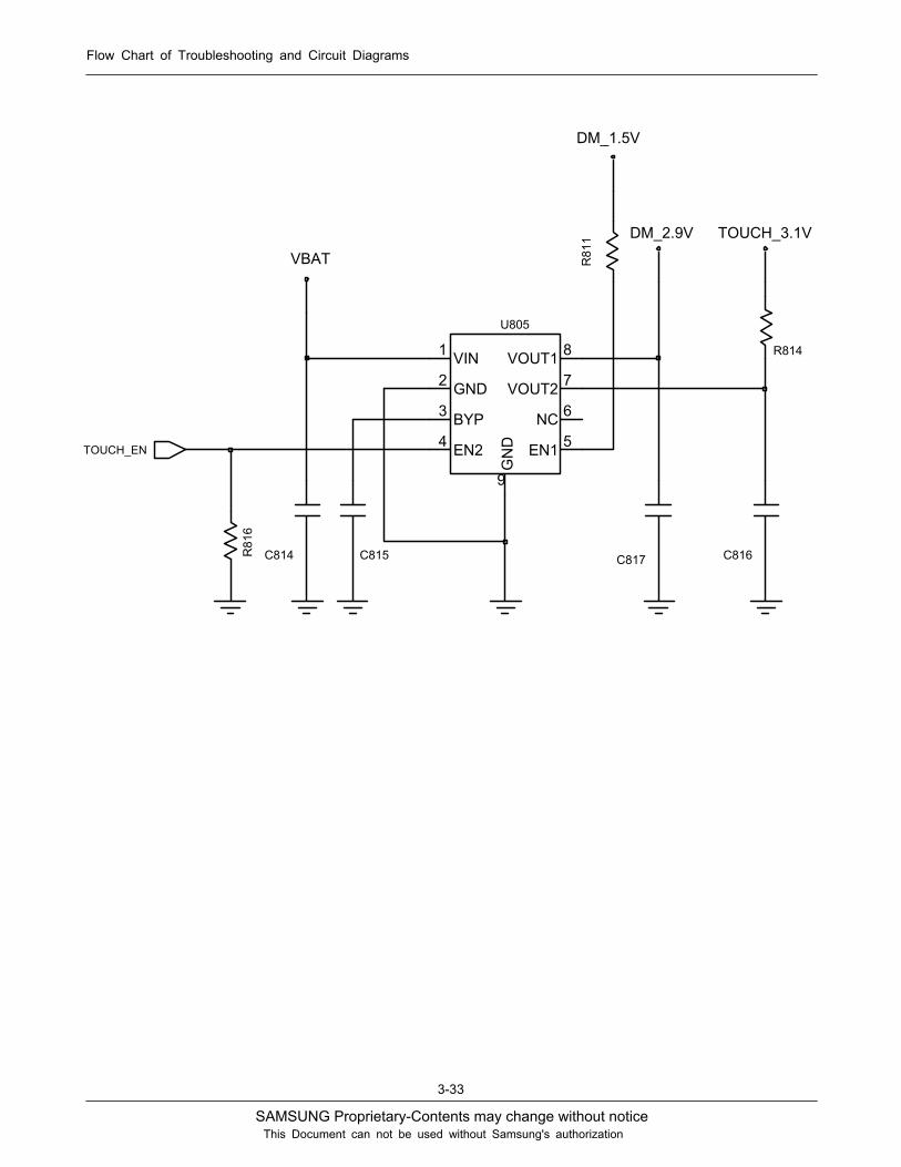
DM_2.9V
8VOUT17VOUT2
3 BYP
EN1 5EN24
2 GND
9
DN
G
6NC
VIN1
U805
618R
TOUCH_3.1V
C817
118R
R814
DM_1.5V
C816C815C814
VBAT
TOUCH_EN

SAMSUNG Proprietary-Contents may change without notice
Flow Chart of Troubleshooting and Circuit Diagrams
3-34
This Document can not be used without Samsung's authorization
104DZ
1 2 3456
114C
1 2 3456
7 8
INNER_BAT
304DZ
424C
74C
NC
N84 9 4
CN
CN
05
4343 44444545 4646
5 5 6 677 88
9 9
37 37 38 3839 39
44
40404141 4242
33
30 30
3131 323233 33 34 34
3535 3636
22 22
2323 242425 25 26 26
2727 282829 29
14 14
1515 161617 17 1818
1919
2 2
202021 21
SOC400
1 1
10 10
1111 121213 13
EXT_BAT
R439R438
EXT_BAT
R436
504DZ
R441R440
R437
R432
014C
EXT_CF
3_YEK
1_YEK
V_MOT
TOUCH_SCL
SCAN_3
INNER_CF
SCAN_5KEY_3.3V
MIC1P
HW_RST
KEY_2
TOUCH_OK
TOUCH_SDATOUCH_RESETTOUCH_3.1VKEY_1KEY_3SCAN_4SCAN_6MIC1N
CAM
KEY_0
TOUCH_OK

SAMSUNG Proprietary-Contents may change without notice
Flow Chart of Troubleshooting and Circuit Diagrams
3-35
This Document can not be used without Samsung's authorization

SAMSUNG Proprietary-Contents may change without notice
Flow Chart of Troubleshooting and Circuit Diagrams
3-36
This Document can not be used without Samsung's authorization
2.RF3-2-1. EGSM Receiver
Rx ONRF Input : 62Ch
Cell Pwr : -50dBm
YES
Normal conditionCatch the channel
END
Check Intenna SolderingANTCON100, ANTCON101
NO
NO Resolder or change RFSW100RFSW100(RF Switch)Pin#1 ≥ -60dBm ?
FEM100Pin#12,13 ≥ -60dBm ?
U100Pin#37,38 ≥ -60dBm ?
Check the UCP300
NO Check or resolder L104, L106,L122, L123 or U100
FEM100Pin#9,10 = LOW &Pin#11 = HIGH ?
Resolder or change FEM100
Check FEM100 control path
YES
YES
YES
YES
NO
NO
YES

SAMSUNG Proprietary-Contents may change without notice
Flow Chart of Troubleshooting and Circuit Diagrams
3-37
This Document can not be used without Samsung's authorization
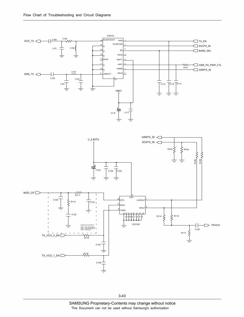
3-2-2. EGSM Transmitter
Tx ONRF Level : 5
YES
Normal conditionCatch the channel
NO
NORFSW100(RF Switch)Pin#1 ≥ 30dBm ?
END
Check the UCP300
YES
NO
Check Intenna SolderingANTCON100, ANTCON101
Resolder or change RFSW100
Check R103, R106Resolder or change VCO100
FEM100Pin#9,10 = HIGH &
Pin#11 = LOW ?
Resolder or change FEM100
Check FEM100 control pathNO
YES
VCO100Pin#1 ≒ 6dBm ?
PAM100Pin#9 ≥ 30dBm ?
FEM100Pin#22 ≥ 30dBm ?
Check C137, C139≥ 1V ?
NO Check C108, C155, C156, L121Resolder or change PAM100
Check Loop filter circuitC129, C131, C132, R111, R112
NO
NO
YES
YES
YES
YES
SAMSUNG Proprietary-Contents may change without notice
Flow Chart of Troubleshooting and Circuit Diagrams
3-38
This Document can not be used without Samsung's authorization
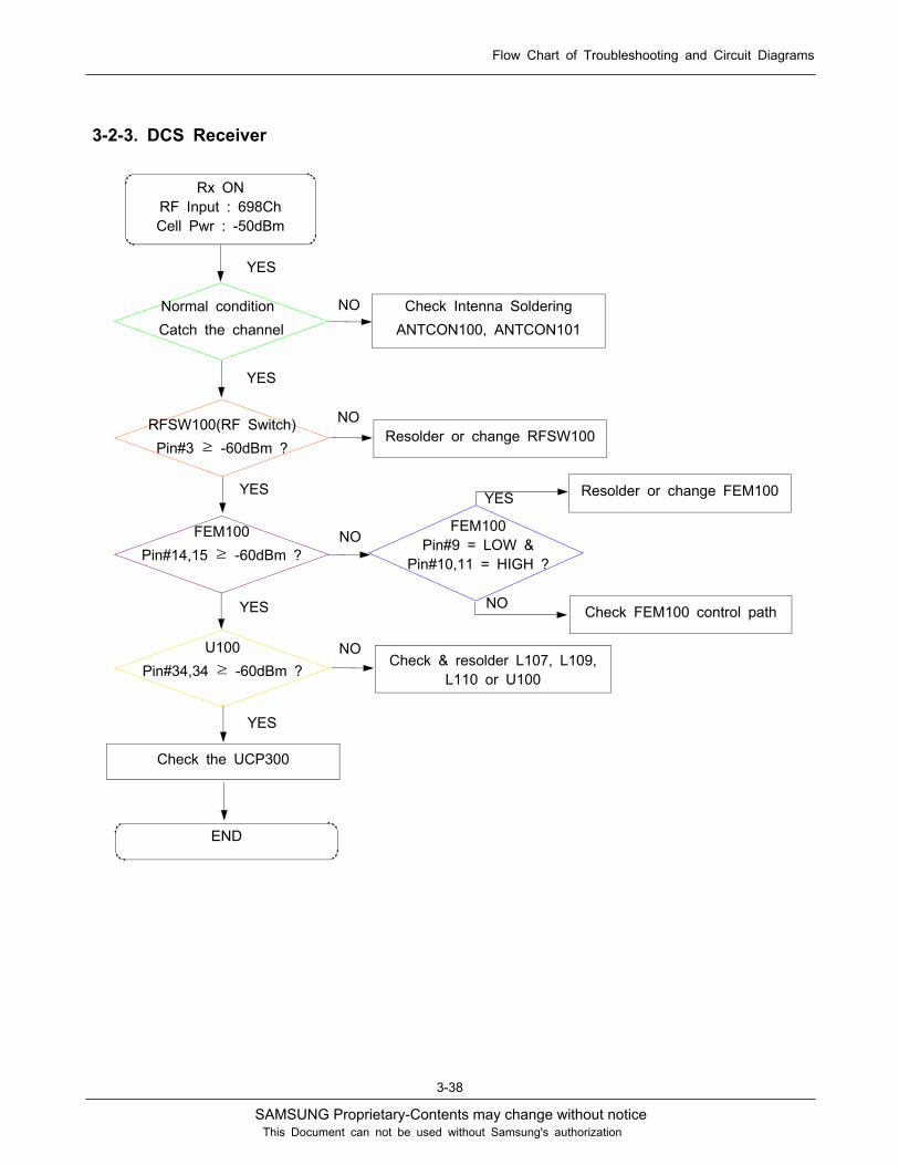
3-2-3. DCS Receiver
Rx ONRF Input : 698ChCell Pwr : -50dBm
YES
Normal conditionCatch the channel
NO
NORFSW100(RF Switch)Pin#3 ≥ -60dBm ?
END
Check the UCP300
YES
NO
Check Intenna SolderingANTCON100, ANTCON101
Resolder or change RFSW100
FEM100Pin#9 = LOW &
Pin#10,11 = HIGH ?
Resolder or change FEM100
Check FEM100 control pathNO
YES
U100Pin#34,34 ≥ -60dBm ?
FEM100Pin#14,15 ≥ -60dBm ?
NOCheck & resolder L107, L109,
L110 or U100
YES
YES
YES

SAMSUNG Proprietary-Contents may change without notice
Flow Chart of Troubleshooting and Circuit Diagrams
3-39
This Document can not be used without Samsung's authorization
3-2-4. DCS Transmitter
Tx ONRF Level : 0
YES
Normal conditionCatch the channel
NO
NORFSW100(RF Switch)Pin#1 ≥ 27dBm ?
END
Check the UCP300
YES
NO
Check Intenna SolderingANTCON100, ANTCON101
Resolder or change RFSW100
Check R104, R108Resolder or change VCO100
FEM100Pin#9 = HIGH &
Pin#10,11 = LOW ?
Resolder or change FEM100
Check FEM100 control pathNO
YES
VCO100Pin#5 ≒ 6dBm ?
PAM100Pin#16 ≥ 27dBm ?
FEM100Pin#20 ≥ 27dBm ?
Check C137, C139≥ 1V ?
NOCheck C105, C106, C157, L103
Resolder or change PAM100
Check Loop filter circuitC129, C131, C132, R111, R112
NO
NO
YES
YES
YES
YES

SAMSUNG Proprietary-Contents may change without notice
Flow Chart of Troubleshooting and Circuit Diagrams
3-40
This Document can not be used without Samsung's authorization
3-2-5. PCS Receiver
Rx ONRF Input : 661ChCell Pwr : -50dBm
YES
Normal conditionCatch the channel
NO
NORFSW100(RF Switch)Pin#3 ≥ -60dBm ?
END
Check the UCP300
YES
NO
Check Intenna SolderingANTCON100, ANTCON101
Resolder or change RFSW100
FEM100Pin#9,11 = LOW &Pin#10 = HIGH ?
Resolder or change FEM100
Check FEM100 control pathNO
YES
U100Pin#24,35 ≥ -60dBm ?
FEM100Pin#16,17 ≥ -60dBm ?
NOCheck & resolder U100
YES
YES
YES

SAMSUNG Proprietary-Contents may change without notice
Flow Chart of Troubleshooting and Circuit Diagrams
3-41
This Document can not be used without Samsung's authorization
3-2-6. PCS Transmitter
Tx ONRF Level : 0
YES
Normal conditionCatch the channel
NO
NORFSW100(RF Switch)Pin#1 ≥ 27dBm ?
END
Check the UCP300
YES
NO
Check Intenna SolderingANTCON100, ANTCON101
Resolder or change RFSW100
Check R104, R108Resolder or change VCO100
FEM100Pin#9 = HIGH &
Pin#10,11 = LOW ?
Resolder or change FEM100
Check FEM100 control pathNO
YES
VCO100Pin#5 ≒ 6dBm ?
PAM100Pin#16 ≥ 27dBm ?
FEM100Pin#20 ≥ 27dBm ?
Check C137, C139≥ 1V ?
NOCheck C105, C106, C157, L103
Resolder or change PAM100
Check Loop filter circuitC129, C131, C132, R111, R112
NO
NO
YES
YES
YES
YES

SAMSUNG Proprietary-Contents may change without notice
Flow Chart of Troubleshooting and Circuit Diagrams
3-42
This Document can not be used without Samsung's authorization
C139
C137
C133
R122
V_2.85TX
C122
R115
C144
L117
C148
C142
C150
C136
C145
C141
C128
V_2.85TX
C153
L119
R120
V_2.6P
R107
C127
C130
901R
L118
C120
R121
C143
R110
L116
L113
V_2.85OSC
C121
L115
C147
C140
C149
V_2.85OSC
V_2.85TX R105
L114
V_2.85TX
C126
27VDDA8
31
9A
DD
V
43
MD
DV
8
FE
R_E
NUTV
54 VDDA16
56 VDDA17
5
2A
DDV
7
3A
DDV
10
4A
DDV
155
AD
DV
23VDDA6
26VDDA7
9
EN
UT_O
CV
4
1A
DDV
36
01A
DDV
39
11A
DDV
41
21A
DDV
48 VDDA13
50 VDDA14
52 VDDA15
40
PC_
DO
M_XT
17TX_QN
16TX_QP
42
BF_O
CV_XT
53 UMTS1900_OUT
51 UMTS2100_OUT
55 UMTS800_OUT
49 VCONTROL
32
NI_O
CV_XR
33
SAI
B_R44 SBCK
45 SBDT
46 SBST
6
OXCT
19TX_IN
18TX_IP
37
PNI_009
MS
G
58NC159NC2
47 RF_ON
14
NI_XR
13
PI_XR
12
NQ_X
R
11
PQ_X
R
57 GND
34
NNI_0081
MS
G
35
PNI_0081
MSG
24GSM1900_INN
25GSM1900_INP
21GSM850_INN
22GSM850_INP
38
NNI_009
MSG
2
1PC
30
2P
C
1
1DL
OH_P
C
29
2DL
OH_
PC
20DAC_REF
3
1Q
AF
28FAQ2
U100
OC
VXT
PC_
DO
M
PXR_
MS
G
NXR_
MS
GUMTS_TXRF
SBST
SBDT
SBCK
PQ_X
R
MQ_X
R
PI_X
R
MI_X
R
RF_ON_TX_ON
PCS_RXP
PCS_RXN
PXR_S
CD
NXR_S
CD
DAC_REF
UMTS_RX_TUNE
VCO_TUNE
EN
UT_O
CV
TX_AGC_ADJ
OX
CT
TX_QP
TX_QM
TX_IP
TX_IM
UMTS_RX_VCO_IN
SAMSUNG Proprietary-Contents may change without notice
Flow Chart of Troubleshooting and Circuit Diagrams
3-43
This Document can not be used without Samsung's authorization
C634 : COG type(30ppm)
Qualcomm recommend
C635 : COG type(30ppm)C636 : CPPS type
R114
601R
R116
R111
C138
C129
R11313
GG
14
HIOUT 5
1LOWOUT
3VCC
10 VCTL
VSW111
9 VSW2
2
G
4
G
6
GG
78
GG
12
VCO100
V_2.85TX
C134
801R
C123
C131
C132
R118
C125
R103
C124
R112
R117
R104
C135
MOD_CP
DCSTX_IN
GSMTX_IN
TXVCO
TX_VCO_1_EN
TX_VCO_0_EN
VBAT
C113C116
L121
C157
C105
9
4RSVD
8RSVD
RSVD12
1TXEN
VAPC 6
5VBATT
DCS|PCSOUT16
G13
G10
11G
14G
G15
17
G
GSMIN 7
GSMOUT
PAM100
3BS
2DCS|PCSIN
C115
C108
L103
C155
C118
C156
C106
R101
C117
DCS_TX
GSM_TX
GSMTX_IN
DCSTX_IN
BAND_SEL
TX_EN
GSM_PA_PWR_CTL

SAMSUNG Proprietary-Contents may change without notice
Flow Chart of Troubleshooting and Circuit Diagrams
3-44
This Document can not be used without Samsung's authorization
C11
1L1
07
C15
8
R12
3
V_2
.85R
X
L109
C10
1
4
AN
TCO
N10
112 2
3 3
4
L111
L120
L112
L104
C10
4
1 122334
4
ANTC
ON
20
L124
321L
C10
3
C10
0
L110
C11
0
L106
11
VDD
8
GG
24
3N
C
PC
S_R
X16
PCS_
RX
17U
MTS
2100
4
V1
9 10V
2V
3 EGSM
_TX
1GG 2
5GG 718
GG 19
21G 23
TNA
6
14D
CS_
RX
15D
CS
_RX
DC
S|PC
S_T
X20
12E
GSM
_RX
EG
SM_R
X13
22
FEM
100
L101
G 4
RFS
W10
0
A 2C 1
3G
001L
C10
2
221L
C11
2
GS
M_R
XN
GS
M_R
XP
PC
S_R
XN
PC
S_R
XP
AN
T_S
EL1
_NA
NT_
SE
L2_N
AN
T_S
EL0
_N
DC
S_R
XN
DC
S_R
XP
DC
S_T
XG
SM
_TX
UM
TS_A
NT
SAMSUNG Proprietary-Contents may change without notice
Flow Chart of Troubleshooting and Circuit Diagrams
3-45
This Document can not be used without Samsung's authorization

SAMSUNG Proprietary-Contents may change without notice
Flow Chart of Troubleshooting and Circuit Diagrams
3-46
This Document can not be used without Samsung's authorization
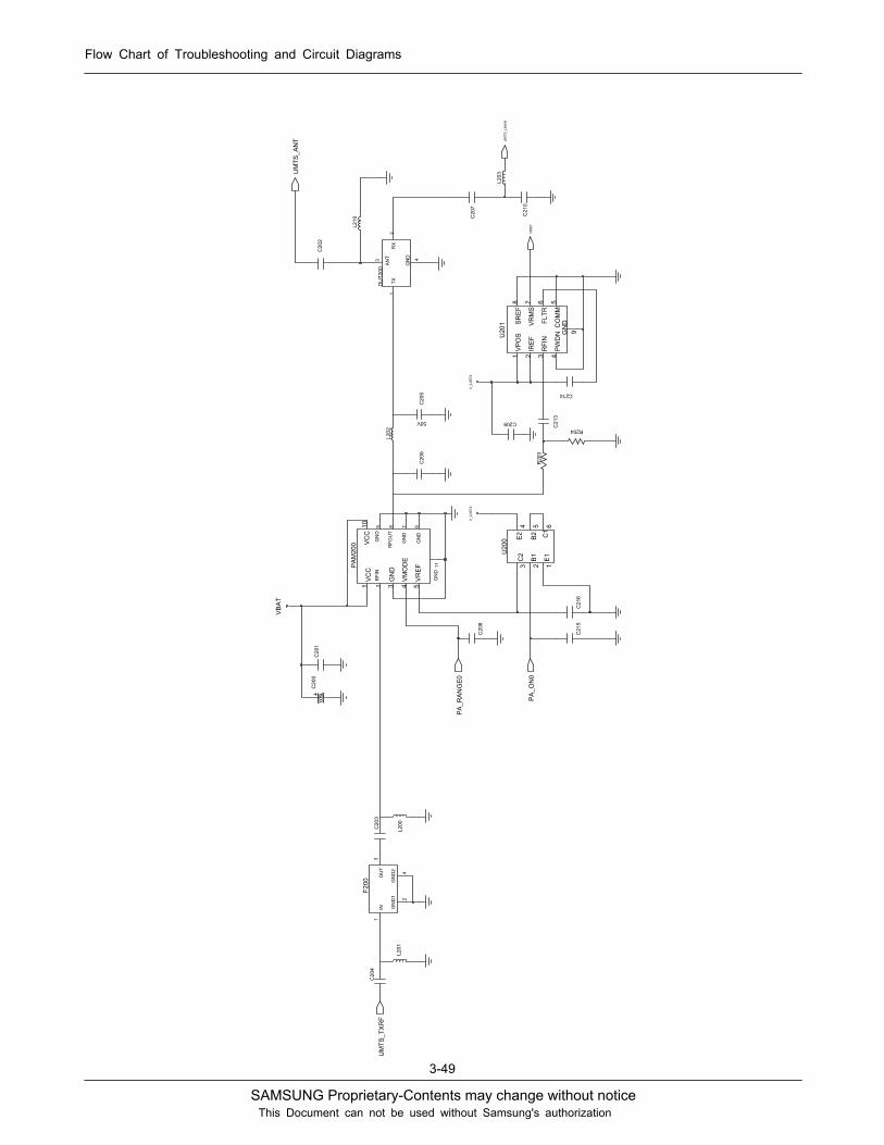
3-2-7. UMTS Receiver
Rx ONRF Input : 10700ChCell Pwr : -40dBm
YES
Normal conditionCatch the channel
NO
NO
END
Check the UCP300
NO
Resolder or change RFSW100
FEM100Pin#9,11 = HIGH &
Pin#10 = LOW ?
Resolder or change FEM100
Check FEM100 control pathNO
YES
NO
YES
RFSW100(RF Switch)Pin#1, 2 ≥ -50dBm ?
FEM100Pin#4 ≥ -50dBm ?
DUT200Pin#2 ≥ -50dBm ?
U202Pin#18 ≥ -65dBm ?
YES
U202Pin#18 ≥ -65dBm ?
F201Pin3, 4 ≥ -65dBm ?
U202Pin8, 9 ≥ -65dBm ?
Resolder or change C207, L203
NOResolder C202 or
change DUT200
NOResolder or change U202
NOCheck the path of F201 & U202
NO
Check Intenna SolderingANTCON100, ANTCON101
Check the path of F201 & U202

SAMSUNG Proprietary-Contents may change without notice
Flow Chart of Troubleshooting and Circuit Diagrams
3-47
This Document can not be used without Samsung's authorization
3-2-8. UMTS Transmitter
Tx ONRF Input : 9750ChCell Pwr : 24dBm
YES
Normal conditionCatch the channel
NO
NO
END
Check the UCP300
NO
Resolder or change RFSW100
FEM100Pin#9,11 = HIGH &
Pin#10 = LOW ?
Resolder or change FEM100
Check FEM100 control pathNO
YES
NO
YES
RFSW100(RF Switch)Pin#1, 2 ≥ 20dBm ?
FEM100Pin#4 ≥ 20dBm ?
DUT200Pin#3 ≥ 20dBm ?
PAM200Pin#8 ≥ 20dBm ?
YES
F200Pin#3 ≥ -2dBm ?
U100Pin51 ≥ -2dBm ?
Check C137, C139≥ 1V ?
Check PAM200 pin#5 = HIGH ?Resolder or change F200
NOResolder C202 or
change DUT200
NOCheck C203, C204
Resolder or change F200
NOCheck the path of U100
NO
Check Intenna SolderingANTCON100, ANTCON101
Check or resolder UCP300

SAMSUNG Proprietary-Contents may change without notice
Flow Chart of Troubleshooting and Circuit Diagrams
3-48
This Document can not be used without Samsung's authorization
C244
L209
V_2.85TCXO
L204
R206
V_2.85RX1
R210
C240C237
C242
V_2.85TCXO
C225
32
34VDDA6
36VDDA7
548
AD
DV
14M
DDV
VDDRF13
912F
RD
DV
12 VDDRF3
3444T
SB
S
33TCXO
25UMTS_TUNE
7 VDDA1
2A
DD
V42
26VDDA327VDDA4
VDDA5
10
11 PMIXP
12MI_
XR
02PI_
XR
32M
Q_X
R
PQ_
XR
22
64S
AIB_
R
24K
CB
S
TD
BS
8 IMIXM
9 IMIXP LO_OUT 28
1C
N0515
2C
N
51S
AIB_
ANL
P
61NI_
ANL
P
31T
UO_
ANL
P
PMIXM
35GPS_TUNE
93MI_X
RG
04PI_
XR
G
MQ_
XR
G73
PQ_
XR
G83
71S
AIB_
ANLI
NI_A
NLI8141
TU
O_A
NLI
31FAQ
84S
AIB_
ANL
G
74NI_
ANL
G
1 GLNA_OUT
GMIXM5
6 GMIXP
4 GND1
942
DN
G
U202
2 BLANK
29CP_DUMP
CP_OUT 30
L208
L207
V_2.85TCXO
V_2.6P
C239
R208 V_2.85TCXO
C241
C248
C224
C226
C228
C222
R207
C243
C238
C247
L205
4OUT
L206
F201G
2
G
5
1IN
3OUT
C245C246
C223
C227
UMTS_RXP
UMTS_RX_VCO_IN
MI_X
R
PI_X
R
MQ_
XR
PQ_
XR
KC
BS
TD
BS
TSB
S
UMTS_RX_TUNE
TCXO
UMTS_RXM
NIA
NL_ST
MU
UMTS_RXM
UMTS_RXP
SAMSUNG Proprietary-Contents may change without notice
Flow Chart of Troubleshooting and Circuit Diagrams
3-49
This Document can not be used without Samsung's authorization
402 R
VBA
T
L203
V_2.
85TX
V05
C20
5
L202
V_2.
85TX
412 C
C20
2
C20
3
C21
0
C20
1
1
7V
RM
S
5C
OM
M
FLTR
6
9GN
D
2IR
EF
PW
DN
43R
FIN
SR
EF8
VPO
SU20
1
C20
0
2
GN
D1
GN
D2 4
1IN
3O
UT
F200
C20
8
L210
L200
902 C
L201
C20
4
C20
6
7G
ND
RFI
N2
RFO
UT
8
VC
C1
VC
C10
VM
OD
E4
VR
EF53
GN
D
6G
ND
9G
ND
11G
ND
PAM
200
C21
5C
216
R20
3E
11
4E2
C21
3
U20
0
2B
15
B2 C1
6
C2
3
C20
7
TX1
DU
T200
3
AN
T
GN
D 4
RX
2
PA
_ON
0H
DE
T
PA_R
AN
GE0
UM
TS_L
NAI
N
UM
TS_A
NT
UM
TS_T
XR
F

SAMSUNG Proprietary-Contents may change without notice
Flow Chart of Troubleshooting and Circuit Diagrams
3-50
This Document can not be used without Samsung's authorization

SAMSUNG Proprietary-Contents may change without notice
Flow Chart of Troubleshooting and Circuit Diagrams
3-51
This Document can not be used without Samsung's authorization
3-2-9. BLUETOOTH
Bluetooth does not work
END
NO
Resolder or Change U501NO
Check the assembled statusof BT_ANT
YES
Check BT function ActivationON ?
NO
YES
Check C218, C236 ≒3V
Check signal on C230Frequency ≒ 26MHz
Check RF Power ≒ 2dBmat R209
YES
YES
YES
Resolder or Change OSC200NO
Resolder or Change U203NO
Resolder or Change BT_ANT
Enable BT function

SAMSUNG Proprietary-Contents may change without notice
Flow Chart of Troubleshooting and Circuit Diagrams
3-52
This Document can not be used without Samsung's authorization
R205
C218
152C
12
3
TN
A_TB
R209
942C
3
1
002CS
O
2
4
C235
C232
912C
C234
C221C220
C229
XTAL_OUTL4
AN
A_D
DV5L
ER
OC_
DDV
6L
VREG_INL7
USB_DNL8
USB_DPL9
AIO2K7
PIO6K8
PIO7K9
AUDIO_IN_P_RIGHTL1
BS
U_D
DV01L
UART_RTSL11
AUDIO_IN_N_RIGHTL2
XTAL_INL3
FR_S
SV1
K
SD
AP_S
SV01
K
UART_CTSK11
AUDIO_IN_P_LEFTK2
AUDIO_IN_N_LEFTK3
AN
A_SSV
4K
AIO0K5
MEM_
DDV
6K
OL_D
DV2J
AUDIO_OUT_N_LEFTJ3
AUDIO_OUT_P_LEFTJ4
AUDIO_OUT_N_RIGHTJ5
AUDIO_OUT_P_RIGHTJ6
AIO1J7
AIO3J8
PIO5J9
PCM_CLKH10
PCM_INH11
NCH2
OL_SSV
3H
PIO4H9
FR_S
SV1J
UART_TXJ10
UART_RXJ11
RESETF9
LA
B_SSV
1G
PCM_OUTG10
PCM_SYNCG11
OID
AR_S
SV2
G
OL_SSV
3G
RESETBG9
NCH1
OID
AR_S
SV2E
OID
AR_
DD
V3E
TEST_ENE9
LA
B_D
DV
1F
ER
OC_S
SV01F
ER
OC_
DDV
11F
NCF2
OID
AR_S
SV3F
SPI_CLKD10
SPI_MOSID11
RF_IND2
PIO0|RXEND3
SD
AP_S
SV9
D
NCE1
SD
AP_S
SV01E
SD
AP_
DD
V11
E
PIO2C3
PIO1|TXENC4
ME
M_SSV
5C
ER
OC_S
SV6
CE
RO
C_D
DV
7C
MEM_
DDV
8C
SSV
9C
NCD1
NCB6
NCB7
NCB8
NCB9
NCC1
SPI_CSBC10
SPI_MISOC11
AUX_DACC2
NCA9
RF_CONNECTB1
NCB10
MEM_
DDV
11B
PIO3B2
PIO8B3
PIO9B4
NCB5
NCA11
OIP_S
SV2
AOI
P_D
DV3
A
PIO10A4
PIO11A5
NCA6
NCA7
NCA8
U203
NC1
NC2
BAL_MATCHA1
NCA10
252C
C217
V_BT_3.05V
C233
C231
052C
032C
632C
V_BT_3.05V
AK_BT_RAK_BT_L
AUX_PCM_DINAUX_PCM_DOUT
AUX_PCM_SYNC
AUX_PCM_CLK
BT_RTS
BT_RXDBT_TXDBT_CTS

SAMSUNG Proprietary-Contents may change without notice
Flow Chart of Troubleshooting and Circuit Diagrams
3-53
This Document can not be used without Samsung's authorization

SAMSUNG Proprietary-Contents may change without notice
4. Array course control
4-1
This Document can not be used without Samsung's authorization
Test Cable (GH39-00478A)
RF Test Cable (GH39-00737A)
Test Jig (GH80-03308A)

SAMSUNG Proprietary-Contents may change without notice
Array course control
4-2
This Document can not be used without Samsung's authorization
Software Downloading
4-1. Downloading Binary Files• Three binary files for downloading F500.– VIC_SEC : Main source code binary folder.– SECUMTS_rsc.bin : Resource file
4-2. Pre-requsite for Downloading• Downloader Program([VISTA]U-Medic_v1.3.3.exe)• F500 Mobile Phone• Data Cable• Binary files

SAMSUNG Proprietary-Contents may change without notice
Array course control
4-3
This Document can not be used without Samsung's authorization
4-3. S/W Downloader Program1. Load the binary download program by executing the “[VISTA]U-Medic_v1.3.3.exe”
Then, check the every "check box" which is "Erase NAND", "Change Boot Area","Code" and "Resource".

SAMSUNG Proprietary-Contents may change without notice
Array course control
4-4
This Document can not be used without Samsung's authorization
2. Click the Broswer button and select the folder. (Select Code and Resource)
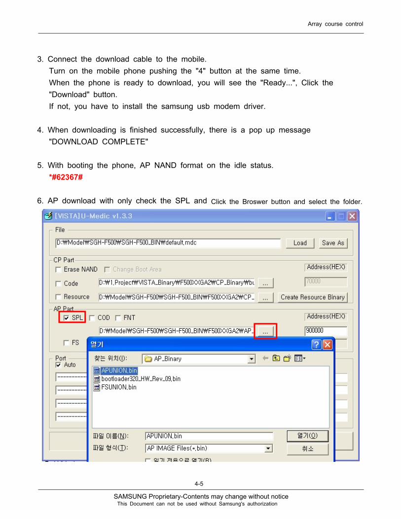
SAMSUNG Proprietary-Contents may change without notice
Array course control
4-5
This Document can not be used without Samsung's authorization
3. Connect the download cable to the mobile.Turn on the mobile phone pushing the "4" button at the same time.When the phone is ready to download, you will see the "Ready...", Click the"Download" button.If not, you have to install the samsung usb modem driver.
4. When downloading is finished successfully, there is a pop up message"DOWNLOAD COMPLETE"
5. With booting the phone, AP NAND format on the idle status.*#62367#
6. AP download with only check the SPL and Click the Broswer button and select the folder.

SAMSUNG Proprietary-Contents may change without notice
Array course control
4-6
This Document can not be used without Samsung's authorization
7. After completing download, click the every check box, "SPL", "COD", "FNT" and "FS"
8. Confirm the downloaded version name and etc. :*#1234#Full Reset :*2767*3855#

SAMSUNG Proprietary-Contents may change without notice
5. Block Diagrams
5-1
This Document can not be used without Samsung's authorization
1G Nand + 512 SDRAM
(Memory)
MSM6275
TMS320DM340ZVL
keypad
Main MIC
Ear MIC
Ear SPK
MAX
9722
SAPA1D1
SPK+
SPK+
DDR
512MB
MoviNAND
512MB
AK2443
LCD (1.5inch)
LCD (2.4inch)
CAMERA(2M CMOS)
Touch_Key
T-Flash
RTR6250
GSM/UMTS
Transceiver
UCVA4XW30AGSM Dual TX VCO
SKY77329-152G/2.5G PAM
FEMEDPXBI5445EAA
ACMD-7601UMTSDuplexer
AWT6277RUMTS PAM
SFDG50AU101Tx SAW filter
PEMD10
SFHG40YS101Rx SAW filter
BC358239A-INN-E4
BT Module
PM6650
Power management
Inner
Battery
External
Battery
RFR6250
UMTS Receiver
V mode(gain control)
V ref
ANT
BT_ANT
S/W
TCXO
(19.2MHz)
OSC
(26MHz)
OSC (48MHz)
for USB
OSC
(32.768MHz)
OSC
(27MHz)
OSC(24MHz)
for USB

6. PCB Diagrams
6-1
01N
OCT
NA
02N
OCT
NA
AP_CS
BAT500
BOOT_SW
BOTHHOLE900
006
NC
CN900
D+_J
003
D10
3D
DM_PWR_DN
DM_WAKE_UP
002T
UD
D_J
006F
IM
E10
6FI
ME 2
06FI
ME
008F
IM
E20
8FI
ME
108F
IM
E30
8FI
ME
408F
IM
E
EMU0EMU1
002F F201
109F
409F
309F
209F
GND_J
004
NCF
I
JIG_J
JTAG800
004
DAP
YEK
OSC300
007
CS
O10
7CS
O00
2MA
P
Q900
001
WSF
R
RXD_J
SCN800
SPKPAD600
TP300
TXD_J
002
U
U201
202
U
104
U
U402 304
UU405
U406
206
U
406
U
407
U
408
U
808
U
908
U
U903
U906
U917
819
U
919
U
129
U02
9U
229
U32
9U
U92472
9UUCP300
USB_VCC_J
V407V408
V600
V601
V606V60780
6V
VBAT_J
ZD402
404
DZ

PCB Diagrams
6-2
TNA_TB
003N
C
008N
C
D302
D400
D500
001M
EF
007G
ATJ
006DS_
M
002C
SO
005CS
O
PAM100
003Q
Q400
005Q
105Q
Q502
SIM600
004C
OS
002TS
TCXO100
TP500
TP501
001U
U203
004U
404U
105U
205U
006U
U605
606U
U607806
U
U609
U610
116U
U700
008U
108U
208U
308U
508U
U807
409U
U907
U912
419U
U915
U916
529U
U926
003V103V
004V
104V
204V
V403
V405
306V
406V
V605
001O
CV
ZD401ZD403
504DZ
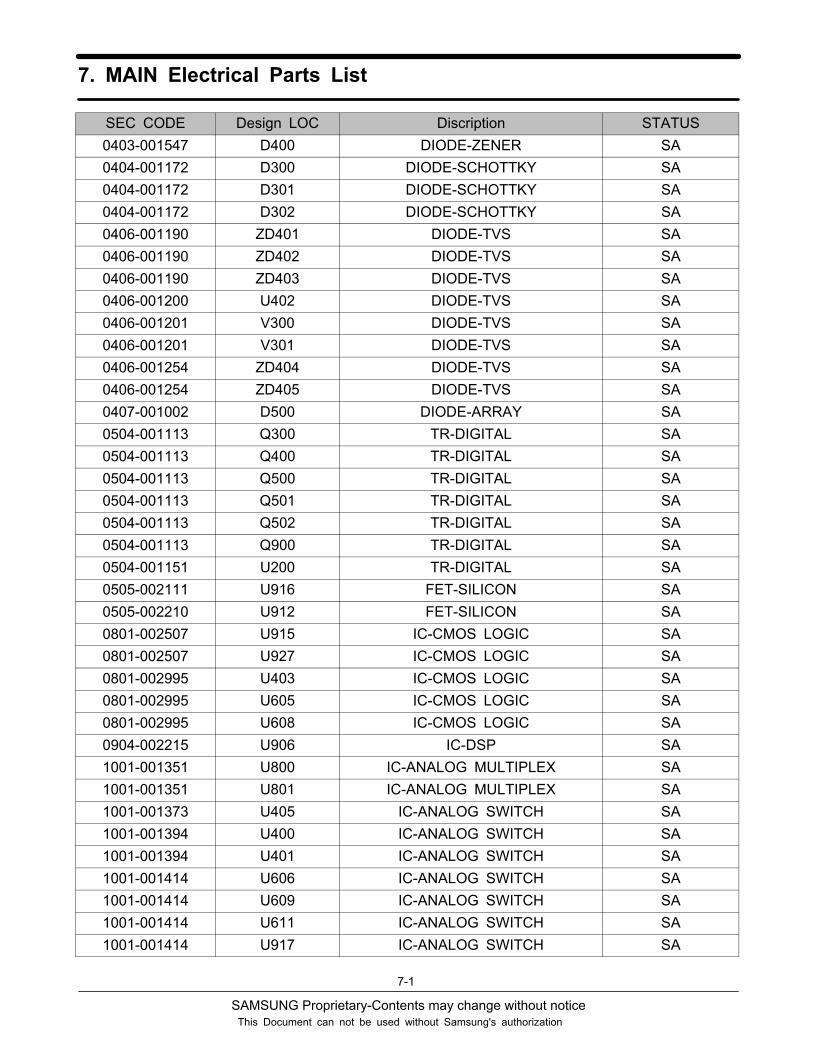
SAMSUNG Proprietary-Contents may change without notice
7-1
This Document can not be used without Samsung's authorization
7. MAIN Electrical Parts List
SEC CODE Design LOC Discription STATUS0403-001547 D400 DIODE-ZENER SA0404-001172 D300 DIODE-SCHOTTKY SA0404-001172 D301 DIODE-SCHOTTKY SA0404-001172 D302 DIODE-SCHOTTKY SA0406-001190 ZD401 DIODE-TVS SA0406-001190 ZD402 DIODE-TVS SA0406-001190 ZD403 DIODE-TVS SA0406-001200 U402 DIODE-TVS SA0406-001201 V300 DIODE-TVS SA0406-001201 V301 DIODE-TVS SA0406-001254 ZD404 DIODE-TVS SA0406-001254 ZD405 DIODE-TVS SA0407-001002 D500 DIODE-ARRAY SA0504-001113 Q300 TR-DIGITAL SA0504-001113 Q400 TR-DIGITAL SA0504-001113 Q500 TR-DIGITAL SA0504-001113 Q501 TR-DIGITAL SA0504-001113 Q502 TR-DIGITAL SA0504-001113 Q900 TR-DIGITAL SA0504-001151 U200 TR-DIGITAL SA0505-002111 U916 FET-SILICON SA0505-002210 U912 FET-SILICON SA0801-002507 U915 IC-CMOS LOGIC SA0801-002507 U927 IC-CMOS LOGIC SA0801-002995 U403 IC-CMOS LOGIC SA0801-002995 U605 IC-CMOS LOGIC SA0801-002995 U608 IC-CMOS LOGIC SA0904-002215 U906 IC-DSP SA1001-001351 U800 IC-ANALOG MULTIPLEX SA1001-001351 U801 IC-ANALOG MULTIPLEX SA1001-001373 U405 IC-ANALOG SWITCH SA1001-001394 U400 IC-ANALOG SWITCH SA1001-001394 U401 IC-ANALOG SWITCH SA1001-001414 U606 IC-ANALOG SWITCH SA1001-001414 U609 IC-ANALOG SWITCH SA1001-001414 U611 IC-ANALOG SWITCH SA1001-001414 U917 IC-ANALOG SWITCH SA

SAMSUNG Proprietary-Contents may change without notice
Exploded View and Parts List
7-2
This Document can not be used without Samsung's authorization
SEC CODE Design LOC Discription STATUS1001-001429 U925 IC-ANALOG MULTIPLEX SA1001-001429 U926 IC-ANALOG MULTIPLEX SA1001-001429 U928 IC-ANALOG MULTIPLEX SA1001-001429 U929 IC-ANALOG MULTIPLEX SA1001-001429 U930 IC-ANALOG MULTIPLEX SA1001-001429 U931 IC-ANALOG MULTIPLEX SA1001-001429 U932 IC-ANALOG MULTIPLEX SA1006-001322 U802 IC-LINE TRANSCEIVER SA1105-001751 U704 IC-DRAM SA1107-001678 U808 IC-FLASH MEMORY SA1108-000071 U804 IC-MCP SA1201-002195 U610 IC-AUDIO AMP SA1201-002240 U904 IC-AUDIO AMP SA1201-002347 PAM200 IC-POWER AMP SA1201-002413 U803 IC-VIDEO AMP SA1201-002446 PAM100 IC-POWER AMP SA1202-001068 U907 IC-VOLTAGE COMP. SA1203-003708 U809 IC-DC/DC CONVERTER SA1203-003742 U404 IC-BATTERY SA1203-004102 U501 IC-POWER SUPERVISOR SA1203-004104 U604 IC-DC/DC CONVERTER SA1203-004362 U607 IC-MULTI REG. SA1203-004448 U502 IC-MULTI REG. SA1203-004449 U807 IC-MULTI REG. SA1203-004453 U700 IC-DC/DC CONVERTER SA1203-004655 U805 IC-MULTI REG. SA1205-002645 U100 IC-TRANSCEIVER SA1205-002727 U600 IC-CODEC SA1205-002781 U202 IC-RECEIVER SA1205-002790 UCP300 IC-MODEM SA1205-003038 U203 IC-DATA COMM./GEN. SA1209-001577 U201 IC-DETECTOR SA1209-001731 U406 IC-SENSOR SA1404-001224 ST200 THERMISTOR-NTC SA1405-001108 V400 VARISTOR SA1405-001108 V401 VARISTOR SA1405-001108 V402 VARISTOR SA

SAMSUNG Proprietary-Contents may change without notice
Exploded View and Parts List
7-3
This Document can not be used without Samsung's authorization
SEC CODE Design LOC Discription STATUS1405-001108 V403 VARISTOR SA1405-001108 V405 VARISTOR SA1405-001108 V406 VARISTOR SA1405-001108 V600 VARISTOR SA1405-001108 V601 VARISTOR SA1405-001108 V608 VARISTOR SA1405-001138 V606 VARISTOR SA1405-001138 V607 VARISTOR SA1405-001177 C527 VARISTOR SA1405-001183 V407 VARISTOR SA1405-001183 V408 VARISTOR SA1405-001183 V603 VARISTOR SA1405-001183 V604 VARISTOR SA1405-001183 V605 VARISTOR SA2007-000141 R101 R-CHIP SA2007-000145 R121 R-CHIP SA2007-000148 U914 R-CHIP SA2007-000149 R604 R-CHIP SA2007-000149 R605 R-CHIP SA2007-000151 R615 R-CHIP SA2007-000154 R619 R-CHIP SA2007-000154 R620 R-CHIP SA2007-000154 R624 R-CHIP SA2007-000154 R625 R-CHIP SA2007-000170 R703 R-CHIP SA2007-000170 R707 R-CHIP SA2007-000171 R123 R-CHIP SA2007-000171 R209 R-CHIP SA2007-000171 R407 R-CHIP SA2007-001292 R112 R-CHIP SA2007-001303 R803 R-CHIP SA2007-001329 R402 R-CHIP SA2007-003010 R106 R-CHIP SA2007-007009 R802 R-CHIP SA2007-007135 R442 R-CHIP SA2007-007142 R501 R-CHIP SA2007-007318 R115 R-CHIP SA

SAMSUNG Proprietary-Contents may change without notice
Exploded View and Parts List
7-4
This Document can not be used without Samsung's authorization
SEC CODE Design LOC Discription STATUS2007-007318 R203 R-CHIP SA2007-007318 R204 R-CHIP SA2007-007318 R304 R-CHIP SA2007-007468 R504 R-CHIP SA2007-007491 R109 R-CHIP SA2007-007491 R208 R-CHIP SA2007-007528 R708 R-CHIP SA2007-007528 R717 R-CHIP SA2007-007741 R428 R-CHIP SA2007-007741 R704 R-CHIP SA2007-007766 R305 R-CHIP SA2007-008045 R110 R-CHIP SA2007-008045 R111 R-CHIP SA2007-008045 R116 R-CHIP SA2007-008045 R118 R-CHIP SA2007-008045 R119 R-CHIP SA2007-008045 R206 R-CHIP SA2007-008045 R406 R-CHIP SA2007-008045 R438 R-CHIP SA2007-008045 R439 R-CHIP SA2007-008045 R440 R-CHIP SA2007-008045 R441 R-CHIP SA2007-008045 R817 R-CHIP SA2007-008045 R818 R-CHIP SA2007-008045 R819 R-CHIP SA2007-008045 R820 R-CHIP SA2007-008045 U923 R-CHIP SA2007-008051 R120 R-CHIP SA2007-008052 R105 R-CHIP SA2007-008052 R205 R-CHIP SA2007-008054 R201 R-CHIP SA2007-008055 R1448 R-CHIP SA2007-008055 R1452 R-CHIP SA2007-008055 R1456 R-CHIP SA2007-008055 R302 R-CHIP SA2007-008055 R411 R-CHIP SA2007-008055 R412 R-CHIP SA
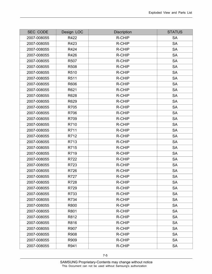
SAMSUNG Proprietary-Contents may change without notice
Exploded View and Parts List
7-5
This Document can not be used without Samsung's authorization
SEC CODE Design LOC Discription STATUS2007-008055 R422 R-CHIP SA2007-008055 R423 R-CHIP SA2007-008055 R424 R-CHIP SA2007-008055 R426 R-CHIP SA2007-008055 R507 R-CHIP SA2007-008055 R508 R-CHIP SA2007-008055 R510 R-CHIP SA2007-008055 R511 R-CHIP SA2007-008055 R606 R-CHIP SA2007-008055 R621 R-CHIP SA2007-008055 R628 R-CHIP SA2007-008055 R629 R-CHIP SA2007-008055 R705 R-CHIP SA2007-008055 R706 R-CHIP SA2007-008055 R709 R-CHIP SA2007-008055 R710 R-CHIP SA2007-008055 R711 R-CHIP SA2007-008055 R712 R-CHIP SA2007-008055 R713 R-CHIP SA2007-008055 R715 R-CHIP SA2007-008055 R719 R-CHIP SA2007-008055 R722 R-CHIP SA2007-008055 R723 R-CHIP SA2007-008055 R726 R-CHIP SA2007-008055 R727 R-CHIP SA2007-008055 R728 R-CHIP SA2007-008055 R729 R-CHIP SA2007-008055 R733 R-CHIP SA2007-008055 R734 R-CHIP SA2007-008055 R800 R-CHIP SA2007-008055 R801 R-CHIP SA2007-008055 R812 R-CHIP SA2007-008055 R816 R-CHIP SA2007-008055 R907 R-CHIP SA2007-008055 R908 R-CHIP SA2007-008055 R909 R-CHIP SA2007-008055 R941 R-CHIP SA
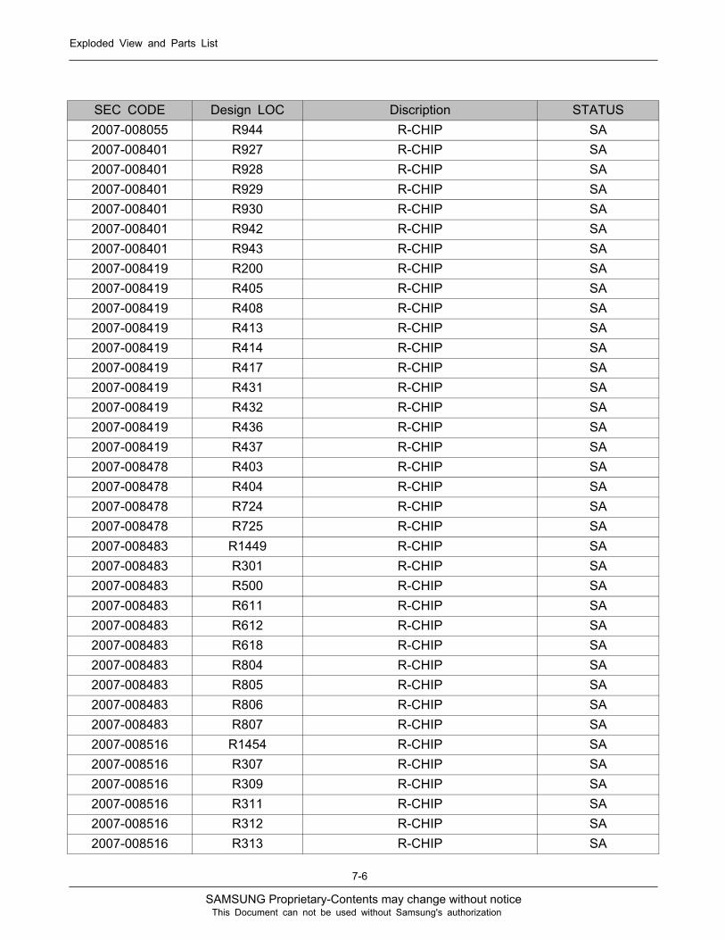
SAMSUNG Proprietary-Contents may change without notice
Exploded View and Parts List
7-6
This Document can not be used without Samsung's authorization
SEC CODE Design LOC Discription STATUS2007-008055 R944 R-CHIP SA2007-008401 R927 R-CHIP SA2007-008401 R928 R-CHIP SA2007-008401 R929 R-CHIP SA2007-008401 R930 R-CHIP SA2007-008401 R942 R-CHIP SA2007-008401 R943 R-CHIP SA2007-008419 R200 R-CHIP SA2007-008419 R405 R-CHIP SA2007-008419 R408 R-CHIP SA2007-008419 R413 R-CHIP SA2007-008419 R414 R-CHIP SA2007-008419 R417 R-CHIP SA2007-008419 R431 R-CHIP SA2007-008419 R432 R-CHIP SA2007-008419 R436 R-CHIP SA2007-008419 R437 R-CHIP SA2007-008478 R403 R-CHIP SA2007-008478 R404 R-CHIP SA2007-008478 R724 R-CHIP SA2007-008478 R725 R-CHIP SA2007-008483 R1449 R-CHIP SA2007-008483 R301 R-CHIP SA2007-008483 R500 R-CHIP SA2007-008483 R611 R-CHIP SA2007-008483 R612 R-CHIP SA2007-008483 R618 R-CHIP SA2007-008483 R804 R-CHIP SA2007-008483 R805 R-CHIP SA2007-008483 R806 R-CHIP SA2007-008483 R807 R-CHIP SA2007-008516 R1454 R-CHIP SA2007-008516 R307 R-CHIP SA2007-008516 R309 R-CHIP SA2007-008516 R311 R-CHIP SA2007-008516 R312 R-CHIP SA2007-008516 R313 R-CHIP SA
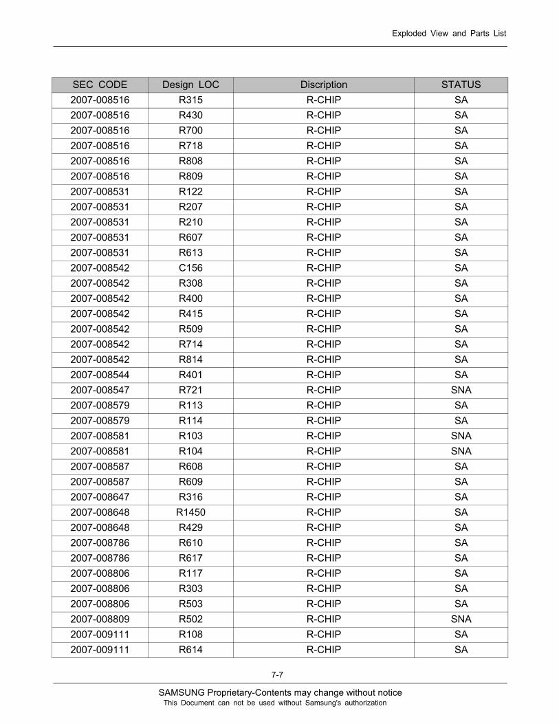
SAMSUNG Proprietary-Contents may change without notice
Exploded View and Parts List
7-7
This Document can not be used without Samsung's authorization
SEC CODE Design LOC Discription STATUS2007-008516 R315 R-CHIP SA2007-008516 R430 R-CHIP SA2007-008516 R700 R-CHIP SA2007-008516 R718 R-CHIP SA2007-008516 R808 R-CHIP SA2007-008516 R809 R-CHIP SA2007-008531 R122 R-CHIP SA2007-008531 R207 R-CHIP SA2007-008531 R210 R-CHIP SA2007-008531 R607 R-CHIP SA2007-008531 R613 R-CHIP SA2007-008542 C156 R-CHIP SA2007-008542 R308 R-CHIP SA2007-008542 R400 R-CHIP SA2007-008542 R415 R-CHIP SA2007-008542 R509 R-CHIP SA2007-008542 R714 R-CHIP SA2007-008542 R814 R-CHIP SA2007-008544 R401 R-CHIP SA2007-008547 R721 R-CHIP SNA2007-008579 R113 R-CHIP SA2007-008579 R114 R-CHIP SA2007-008581 R103 R-CHIP SNA2007-008581 R104 R-CHIP SNA2007-008587 R608 R-CHIP SA2007-008587 R609 R-CHIP SA2007-008647 R316 R-CHIP SA2007-008648 R1450 R-CHIP SA2007-008648 R429 R-CHIP SA2007-008786 R610 R-CHIP SA2007-008786 R617 R-CHIP SA2007-008806 R117 R-CHIP SA2007-008806 R303 R-CHIP SA2007-008806 R503 R-CHIP SA2007-008809 R502 R-CHIP SNA2007-009111 R108 R-CHIP SA2007-009111 R614 R-CHIP SA

SAMSUNG Proprietary-Contents may change without notice
Exploded View and Parts List
7-8
This Document can not be used without Samsung's authorization
SEC CODE Design LOC Discription STATUS2007-009111 R616 R-CHIP SA2007-009111 R631 R-CHIP SA2007-009111 R632 R-CHIP SA2007-009112 R626 R-CHIP SNA2007-009157 R701 R-CHIP SA2007-009157 R716 R-CHIP SA2007-009157 R720 R-CHIP SA2007-009157 R811 R-CHIP SA2007-009158 R427 R-CHIP SA2007-009166 R202 R-CHIP SA2007-009168 R420 R-CHIP SA2007-009168 R421 R-CHIP SA2007-009168 R815 R-CHIP SA2007-009170 R306 R-CHIP SA2007-009170 R310 R-CHIP SA2007-009170 R410 R-CHIP SA2007-009212 R418 R-CHIP SA2007-009212 R813 R-CHIP SA2007-009233 R425 R-CHIP SA2007-009233 R940 R-CHIP SA2007-009244 R107 R-CHIP SA2203-000233 C213 C-CER,CHIP SA2203-000254 C201 C-CER,CHIP SA2203-000254 C209 C-CER,CHIP SA2203-000254 C218 C-CER,CHIP SA2203-000254 C608 C-CER,CHIP SA2203-000254 C942 C-CER,CHIP SA2203-000278 C207 C-CER,CHIP SA2203-000278 C233 C-CER,CHIP SA2203-000330 C720 C-CER,CHIP SA2203-000330 C721 C-CER,CHIP SA2203-000330 C722 C-CER,CHIP SA2203-000330 C723 C-CER,CHIP SA2203-000438 C141 C-CER,CHIP SA2203-000438 C143 C-CER,CHIP SA2203-000438 C149 C-CER,CHIP SA2203-000438 C416 C-CER,CHIP SA

SAMSUNG Proprietary-Contents may change without notice
Exploded View and Parts List
7-9
This Document can not be used without Samsung's authorization
SEC CODE Design LOC Discription STATUS2203-000489 C323 C-CER,CHIP SA2203-000627 C515 C-CER,CHIP SNA2203-000627 C516 C-CER,CHIP SNA2203-000812 C401 C-CER,CHIP SA2203-001072 C106 C-CER,CHIP SA2203-001153 C113 C-CER,CHIP SA2203-001405 C404 C-CER,CHIP SA2203-001405 C407 C-CER,CHIP SA2203-001405 C604 C-CER,CHIP SA2203-002443 C129 C-CER,CHIP SA2203-002668 C205 C-CER,CHIP SA2203-005050 C206 C-CER,CHIP SA2203-005288 C101 C-CER,CHIP SA2203-005395 C203 C-CER,CHIP SA2203-005481 C628 C-CER,CHIP SA2203-005481 C630 C-CER,CHIP SA2203-005682 C100 C-CER,CHIP SA2203-005682 C104 C-CER,CHIP SA2203-005682 C108 C-CER,CHIP SA2203-005682 C110 C-CER,CHIP SA2203-005682 C111 C-CER,CHIP SA2203-005682 C112 C-CER,CHIP SA2203-005682 C128 C-CER,CHIP SA2203-005682 C142 C-CER,CHIP SA2203-005682 C202 C-CER,CHIP SA2203-005682 C208 C-CER,CHIP SA2203-005682 C215 C-CER,CHIP SA2203-005682 C216 C-CER,CHIP SA2203-005682 C405 C-CER,CHIP SA2203-005682 C406 C-CER,CHIP SA2203-005682 C408 C-CER,CHIP SA2203-005682 C409 C-CER,CHIP SA2203-005683 C243 C-CER,CHIP SA2203-005729 C135 C-CER,CHIP SA2203-005729 C138 C-CER,CHIP SA2203-005729 C220 C-CER,CHIP SA2203-005729 C321 C-CER,CHIP SA
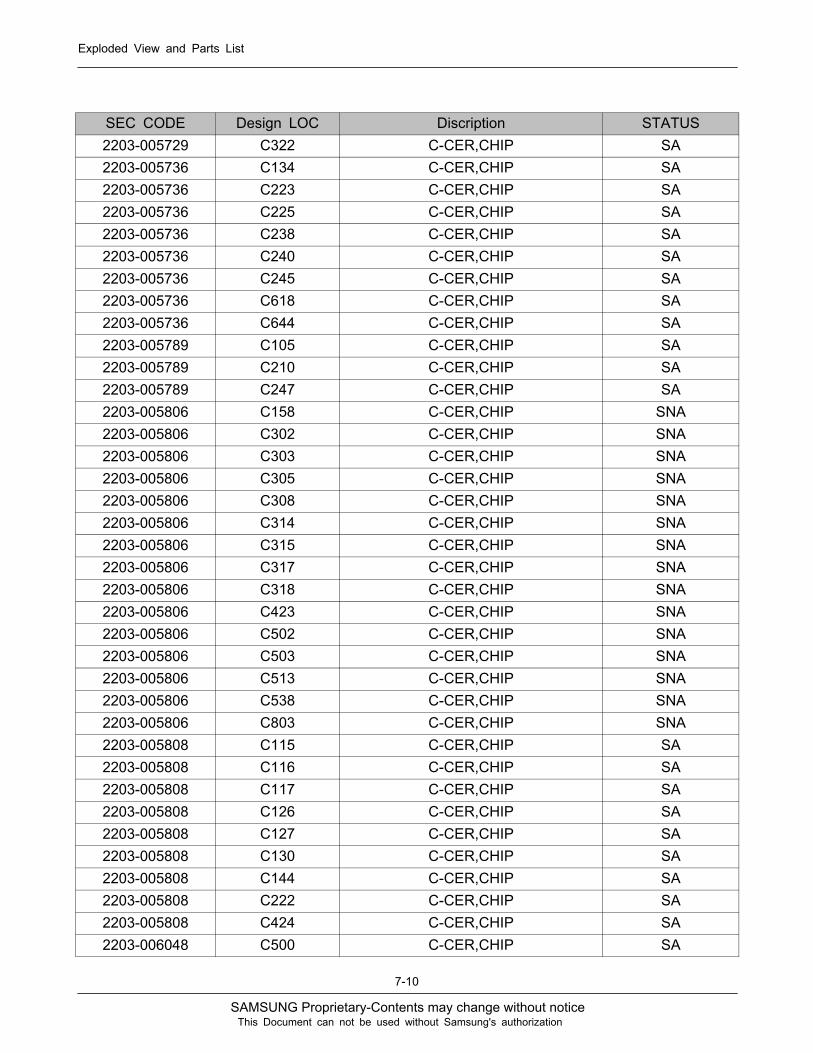
SAMSUNG Proprietary-Contents may change without notice
Exploded View and Parts List
7-10
This Document can not be used without Samsung's authorization
SEC CODE Design LOC Discription STATUS2203-005729 C322 C-CER,CHIP SA2203-005736 C134 C-CER,CHIP SA2203-005736 C223 C-CER,CHIP SA2203-005736 C225 C-CER,CHIP SA2203-005736 C238 C-CER,CHIP SA2203-005736 C240 C-CER,CHIP SA2203-005736 C245 C-CER,CHIP SA2203-005736 C618 C-CER,CHIP SA2203-005736 C644 C-CER,CHIP SA2203-005789 C105 C-CER,CHIP SA2203-005789 C210 C-CER,CHIP SA2203-005789 C247 C-CER,CHIP SA2203-005806 C158 C-CER,CHIP SNA2203-005806 C302 C-CER,CHIP SNA2203-005806 C303 C-CER,CHIP SNA2203-005806 C305 C-CER,CHIP SNA2203-005806 C308 C-CER,CHIP SNA2203-005806 C314 C-CER,CHIP SNA2203-005806 C315 C-CER,CHIP SNA2203-005806 C317 C-CER,CHIP SNA2203-005806 C318 C-CER,CHIP SNA2203-005806 C423 C-CER,CHIP SNA2203-005806 C502 C-CER,CHIP SNA2203-005806 C503 C-CER,CHIP SNA2203-005806 C513 C-CER,CHIP SNA2203-005806 C538 C-CER,CHIP SNA2203-005806 C803 C-CER,CHIP SNA2203-005808 C115 C-CER,CHIP SA2203-005808 C116 C-CER,CHIP SA2203-005808 C117 C-CER,CHIP SA2203-005808 C126 C-CER,CHIP SA2203-005808 C127 C-CER,CHIP SA2203-005808 C130 C-CER,CHIP SA2203-005808 C144 C-CER,CHIP SA2203-005808 C222 C-CER,CHIP SA2203-005808 C424 C-CER,CHIP SA2203-006048 C500 C-CER,CHIP SA

SAMSUNG Proprietary-Contents may change without notice
Exploded View and Parts List
7-11
This Document can not be used without Samsung's authorization
SEC CODE Design LOC Discription STATUS2203-006048 C530 C-CER,CHIP SA2203-006048 C533 C-CER,CHIP SA2203-006048 C536 C-CER,CHIP SA2203-006048 C726 C-CER,CHIP SA2203-006120 C627 C-CER,CHIP SA2203-006120 C629 C-CER,CHIP SA2203-006120 C701 C-CER,CHIP SA2203-006120 C702 C-CER,CHIP SA2203-006120 C708 C-CER,CHIP SA2203-006187 C121 C-CER,CHIP SA2203-006187 C237 C-CER,CHIP SA2203-006187 C246 C-CER,CHIP SA2203-006194 C151 C-CER,CHIP SA2203-006194 C212 C-CER,CHIP SA2203-006194 C221 C-CER,CHIP SA2203-006194 C326 C-CER,CHIP SA2203-006194 C337 C-CER,CHIP SA2203-006194 C534 C-CER,CHIP SA2203-006194 C617 C-CER,CHIP SA2203-006194 C631 C-CER,CHIP SA2203-006194 C662 C-CER,CHIP SA2203-006194 C710 C-CER,CHIP SA2203-006194 C727 C-CER,CHIP SA2203-006194 C728 C-CER,CHIP SA2203-006194 C732 C-CER,CHIP SA2203-006194 C801 C-CER,CHIP SA2203-006194 C802 C-CER,CHIP SA2203-006194 C808 C-CER,CHIP SA2203-006194 C811 C-CER,CHIP SA2203-006194 C823 C-CER,CHIP SA2203-006194 C951 C-CER,CHIP SA2203-006260 C660 C-CER,CHIP SA2203-006260 C663 C-CER,CHIP SA2203-006260 C664 C-CER,CHIP SA2203-006379 C136 C-CER,CHIP SA2203-006379 C421 C-CER,CHIP SA2203-006423 C103 C-CER,CHIP SA

SAMSUNG Proprietary-Contents may change without notice
Exploded View and Parts List
7-12
This Document can not be used without Samsung's authorization
SEC CODE Design LOC Discription STATUS2203-006423 C124 C-CER,CHIP SA2203-006423 C133 C-CER,CHIP SA2203-006423 C140 C-CER,CHIP SA2203-006423 C146 C-CER,CHIP SA2203-006423 C211 C-CER,CHIP SA2203-006423 C214 C-CER,CHIP SA2203-006423 C224 C-CER,CHIP SA2203-006423 C226 C-CER,CHIP SA2203-006423 C227 C-CER,CHIP SA2203-006423 C229 C-CER,CHIP SA2203-006423 C231 C-CER,CHIP SA2203-006423 C232 C-CER,CHIP SA2203-006423 C234 C-CER,CHIP SA2203-006423 C235 C-CER,CHIP SA2203-006423 C239 C-CER,CHIP SA2203-006423 C241 C-CER,CHIP SA2203-006423 C242 C-CER,CHIP SA2203-006423 C244 C-CER,CHIP SA2203-006423 C300 C-CER,CHIP SA2203-006423 C301 C-CER,CHIP SA2203-006423 C306 C-CER,CHIP SA2203-006423 C307 C-CER,CHIP SA2203-006423 C309 C-CER,CHIP SA2203-006423 C310 C-CER,CHIP SA2203-006423 C311 C-CER,CHIP SA2203-006423 C312 C-CER,CHIP SA2203-006423 C316 C-CER,CHIP SA2203-006423 C319 C-CER,CHIP SA2203-006423 C320 C-CER,CHIP SA2203-006423 C327 C-CER,CHIP SA2203-006423 C330 C-CER,CHIP SA2203-006423 C331 C-CER,CHIP SA2203-006423 C333 C-CER,CHIP SA2203-006423 C334 C-CER,CHIP SA2203-006423 C411 C-CER,CHIP SA2203-006423 C418 C-CER,CHIP SA2203-006423 C420 C-CER,CHIP SA

SAMSUNG Proprietary-Contents may change without notice
Exploded View and Parts List
7-13
This Document can not be used without Samsung's authorization
SEC CODE Design LOC Discription STATUS2203-006423 C512 C-CER,CHIP SA2203-006423 C514 C-CER,CHIP SA2203-006423 C517 C-CER,CHIP SA2203-006423 C600 C-CER,CHIP SA2203-006423 C601 C-CER,CHIP SA2203-006423 C605 C-CER,CHIP SA2203-006423 C607 C-CER,CHIP SA2203-006423 C609 C-CER,CHIP SA2203-006423 C610 C-CER,CHIP SA2203-006423 C611 C-CER,CHIP SA2203-006423 C612 C-CER,CHIP SA2203-006423 C613 C-CER,CHIP SA2203-006423 C616 C-CER,CHIP SA2203-006423 C622 C-CER,CHIP SA2203-006423 C623 C-CER,CHIP SA2203-006423 C634 C-CER,CHIP SA2203-006423 C637 C-CER,CHIP SA2203-006423 C652 C-CER,CHIP SA2203-006423 C704 C-CER,CHIP SA2203-006423 C705 C-CER,CHIP SA2203-006423 C706 C-CER,CHIP SA2203-006423 C709 C-CER,CHIP SA2203-006423 C715 C-CER,CHIP SA2203-006423 C717 C-CER,CHIP SA2203-006423 C733 C-CER,CHIP SA2203-006423 C800 C-CER,CHIP SA2203-006423 C804 C-CER,CHIP SA2203-006423 C806 C-CER,CHIP SA2203-006423 C807 C-CER,CHIP SA2203-006423 C809 C-CER,CHIP SA2203-006423 C810 C-CER,CHIP SA2203-006423 C815 C-CER,CHIP SA2203-006423 C820 C-CER,CHIP SA2203-006423 C900 C-CER,CHIP SA2203-006423 C943 C-CER,CHIP SA2203-006423 C944 C-CER,CHIP SA2203-006423 C945 C-CER,CHIP SA

SAMSUNG Proprietary-Contents may change without notice
Exploded View and Parts List
7-14
This Document can not be used without Samsung's authorization
SEC CODE Design LOC Discription STATUS2203-006423 C946 C-CER,CHIP SA2203-006423 C947 C-CER,CHIP SA2203-006423 C948 C-CER,CHIP SA2203-006426 C248 C-CER,CHIP SNA2203-006462 C325 C-CER,CHIP SA2203-006462 C606 C-CER,CHIP SA2203-006556 C137 C-CER,CHIP SA2203-006556 C139 C-CER,CHIP SA2203-006556 C204 C-CER,CHIP SA2203-006562 C125 C-CER,CHIP SA2203-006562 C145 C-CER,CHIP SA2203-006562 C150 C-CER,CHIP SA2203-006562 C153 C-CER,CHIP SA2203-006562 C304 C-CER,CHIP SA2203-006562 C313 C-CER,CHIP SA2203-006562 C403 C-CER,CHIP SA2203-006562 C417 C-CER,CHIP SA2203-006562 C419 C-CER,CHIP SA2203-006562 C511 C-CER,CHIP SA2203-006562 C521 C-CER,CHIP SA2203-006562 C522 C-CER,CHIP SA2203-006562 C523 C-CER,CHIP SA2203-006562 C524 C-CER,CHIP SA2203-006562 C525 C-CER,CHIP SA2203-006562 C526 C-CER,CHIP SA2203-006562 C528 C-CER,CHIP SA2203-006562 C532 C-CER,CHIP SA2203-006562 C535 C-CER,CHIP SA2203-006562 C602 C-CER,CHIP SA2203-006562 C635 C-CER,CHIP SA2203-006562 C638 C-CER,CHIP SA2203-006562 C639 C-CER,CHIP SA2203-006562 C640 C-CER,CHIP SA2203-006562 C642 C-CER,CHIP SA2203-006562 C646 C-CER,CHIP SA2203-006562 C647 C-CER,CHIP SA2203-006562 C649 C-CER,CHIP SA

SAMSUNG Proprietary-Contents may change without notice
Exploded View and Parts List
7-15
This Document can not be used without Samsung's authorization
SEC CODE Design LOC Discription STATUS2203-006562 C654 C-CER,CHIP SA2203-006562 C655 C-CER,CHIP SA2203-006562 C656 C-CER,CHIP SA2203-006562 C659 C-CER,CHIP SA2203-006562 C814 C-CER,CHIP SA2203-006562 C819 C-CER,CHIP SA2203-006562 C824 C-CER,CHIP SA2203-006562 C825 C-CER,CHIP SA2203-006562 C826 C-CER,CHIP SA2203-006562 C827 C-CER,CHIP SA2203-006617 C329 C-CER,CHIP SA2203-006617 C332 C-CER,CHIP SA2203-006648 C324 C-CER,CHIP SA2203-006648 C328 C-CER,CHIP SA2203-006668 C805 C-CER,CHIP SA2203-006674 C230 C-CER,CHIP SNA2203-006681 C413 C-CER,CHIP SA2203-006712 C152 C-CER,CHIP SA2203-006712 C228 C-CER,CHIP SA2203-006824 C507 C-CER,CHIP SA2203-006824 C508 C-CER,CHIP SA2203-006824 C529 C-CER,CHIP SA2203-006824 C657 C-CER,CHIP SA2203-006824 C658 C-CER,CHIP SA2203-006824 C712 C-CER,CHIP SA2203-006824 C713 C-CER,CHIP SA2203-006838 C217 C-CER,CHIP SA2203-006838 C236 C-CER,CHIP SA2203-006838 C504 C-CER,CHIP SA2203-006838 C505 C-CER,CHIP SA2203-006838 C506 C-CER,CHIP SA2203-006838 C509 C-CER,CHIP SA2203-006838 C510 C-CER,CHIP SA2203-006838 C518 C-CER,CHIP SA2203-006838 C519 C-CER,CHIP SA2203-006838 C520 C-CER,CHIP SA2203-006838 C537 C-CER,CHIP SA

SAMSUNG Proprietary-Contents may change without notice
Exploded View and Parts List
7-16
This Document can not be used without Samsung's authorization
SEC CODE Design LOC Discription STATUS2203-006838 C626 C-CER,CHIP SA2203-006838 C641 C-CER,CHIP SA2203-006838 C653 C-CER,CHIP SA2203-006838 C700 C-CER,CHIP SA2203-006838 C703 C-CER,CHIP SA2203-006838 C730 C-CER,CHIP SA2203-006838 C816 C-CER,CHIP SA2203-006838 C817 C-CER,CHIP SA2203-006838 C821 C-CER,CHIP SA2203-006838 C822 C-CER,CHIP SA2203-006840 C335 C-CER,CHIP SA2203-006840 C336 C-CER,CHIP SA2203-006840 C410 C-CER,CHIP SA2203-006840 C415 C-CER,CHIP SA2203-006847 C148 C-CER,CHIP SA2203-006872 C714 C-CER,CHIP SA2203-006872 C719 C-CER,CHIP SA2203-006890 C621 C-CER,CHIP SA2203-006890 C648 C-CER,CHIP SA2203-006890 C650 C-CER,CHIP SA2203-006896 C131 C-CER,CHIP SA2203-006896 C734 C-CER,CHIP SA2301-001200 C132 C-FILM,SMD-PPS SA2301-001213 C122 C-FILM,SMD-PPS SA2301-001735 C120 C-FILM,SMD SA2301-001807 C147 C-FILM,SMD SA2404-001225 C123 C-TA,CHIP SA2404-001268 C200 C-TA,CHIP SA2404-001339 C501 C-TA,CHIP SA2404-001352 C402 C-TA,CHIP SA2404-001377 C400 C-TA,CHIP SA2404-001381 C422 C-TA,CHIP SA2404-001381 C531 C-TA,CHIP SA2404-001381 C624 C-TA,CHIP SA2404-001381 C651 C-TA,CHIP SA2404-001406 C118 C-TA,CHIP SA2404-001411 C412 C-TA,CHIP SA

SAMSUNG Proprietary-Contents may change without notice
Exploded View and Parts List
7-17
This Document can not be used without Samsung's authorization
SEC CODE Design LOC Discription STATUS2703-001178 L124 INDUCTOR-SMD SA2703-001752 L601 INDUCTOR-SMD SA2703-001752 U903 INDUCTOR-SMD SA2703-002170 L210 INDUCTOR-SMD SA2703-002203 L100 INDUCTOR-SMD SA2703-002205 L202 INDUCTOR-SMD SA2703-002551 L101 INDUCTOR-SMD SNA2703-002793 L104 INDUCTOR-SMD SA2703-002793 L106 INDUCTOR-SMD SA2703-002793 L120 INDUCTOR-SMD SA2703-002794 L107 INDUCTOR-SMD SA2703-002794 L110 INDUCTOR-SMD SA2703-002794 L206 INDUCTOR-SMD SA2703-002795 L205 INDUCTOR-SMD SNA2703-002819 L114 INDUCTOR-SMD SA2703-002819 L115 INDUCTOR-SMD SA2703-002819 L116 INDUCTOR-SMD SA2703-002819 L117 INDUCTOR-SMD SA2703-002858 L209 INDUCTOR-SMD SA2703-002870 L113 INDUCTOR-SMD SA2703-002870 L118 INDUCTOR-SMD SA2703-002870 L119 INDUCTOR-SMD SA2703-002900 L109 INDUCTOR-SMD SA2703-002906 L203 INDUCTOR-SMD SA2703-002906 L204 INDUCTOR-SMD SA2703-002906 L208 INDUCTOR-SMD SA2703-002917 L207 INDUCTOR-SMD SA2703-002918 L200 INDUCTOR-SMD SA2703-002919 L122 INDUCTOR-SMD SA2703-002919 L123 INDUCTOR-SMD SA2703-002947 L111 INDUCTOR-SMD SA2703-002947 L112 INDUCTOR-SMD SA2703-002953 C155 INDUCTOR-SMD SA2703-003109 C157 INDUCTOR-SMD SA2703-003127 L201 INDUCTOR-SMD SA2703-003182 L700 INDUCTOR-SMD SA2703-003184 L500 INDUCTOR-SMD SA
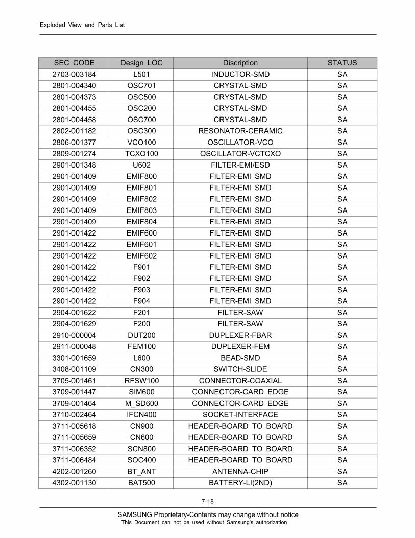
SAMSUNG Proprietary-Contents may change without notice
Exploded View and Parts List
7-18
This Document can not be used without Samsung's authorization
SEC CODE Design LOC Discription STATUS2703-003184 L501 INDUCTOR-SMD SA2801-004340 OSC701 CRYSTAL-SMD SA2801-004373 OSC500 CRYSTAL-SMD SA2801-004455 OSC200 CRYSTAL-SMD SA2801-004458 OSC700 CRYSTAL-SMD SA2802-001182 OSC300 RESONATOR-CERAMIC SA2806-001377 VCO100 OSCILLATOR-VCO SA2809-001274 TCXO100 OSCILLATOR-VCTCXO SA2901-001348 U602 FILTER-EMI/ESD SA2901-001409 EMIF800 FILTER-EMI SMD SA2901-001409 EMIF801 FILTER-EMI SMD SA2901-001409 EMIF802 FILTER-EMI SMD SA2901-001409 EMIF803 FILTER-EMI SMD SA2901-001409 EMIF804 FILTER-EMI SMD SA2901-001422 EMIF600 FILTER-EMI SMD SA2901-001422 EMIF601 FILTER-EMI SMD SA2901-001422 EMIF602 FILTER-EMI SMD SA2901-001422 F901 FILTER-EMI SMD SA2901-001422 F902 FILTER-EMI SMD SA2901-001422 F903 FILTER-EMI SMD SA2901-001422 F904 FILTER-EMI SMD SA2904-001622 F201 FILTER-SAW SA2904-001629 F200 FILTER-SAW SA2910-000004 DUT200 DUPLEXER-FBAR SA2911-000048 FEM100 DUPLEXER-FEM SA3301-001659 L600 BEAD-SMD SA3408-001109 CN300 SWITCH-SLIDE SA3705-001461 RFSW100 CONNECTOR-COAXIAL SA3709-001447 SIM600 CONNECTOR-CARD EDGE SA3709-001464 M_SD600 CONNECTOR-CARD EDGE SA3710-002464 IFCN400 SOCKET-INTERFACE SA3711-005618 CN900 HEADER-BOARD TO BOARD SA3711-005659 CN600 HEADER-BOARD TO BOARD SA3711-006352 SCN800 HEADER-BOARD TO BOARD SA3711-006484 SOC400 HEADER-BOARD TO BOARD SA4202-001260 BT_ANT ANTENNA-CHIP SA4302-001130 BAT500 BATTERY-LI(2ND) SA

SAMSUNG Proprietary-Contents may change without notice
Exploded View and Parts List
7-19
This Document can not be used without Samsung's authorization
SEC CODE Design LOC Discription STATUSGH71-06013A ANTCON10 NPR-ANT CONTACT SAGH71-06013A ANTCON20 NPR-ANT CONTACT SA

SAMSUNG Proprietary-Contents may change without notice
8. Reference data
8-1
This Document can not be used without Samsung's authorization
8-1. Reference Abbreviate
AAC: Advanced Audio Coding.AVC : Advanced Video Coding.BER : Bit Error RateBPSK: Binary Phase Shift KeyingCA : Conditional AccessCDM : Code Division MultiplexingC/I : Carrier to InterferenceDMB : Digital Multimedia BroadcastingEN : European StandardES : Elementary StreamETSI: European Telecommunications Standards InstituteMPEG: Moving Picture Experts GroupPN : Pseudo-random NoisePS : Pilot SymbolQPSK: Quadrature Phase Shift KeyingRS : Reed-SolomonSI : Service InformationTDM : Time Division MultiplexingTS : Transport Stream

SAMSUNG Proprietary-Contents may change without notice
9. Safety Precautions
9-1
This Document can not be used without Samsung's authorization
9-1. Repair Precaution
● Repair in Shield Box, during detailed tuning.Take specially care of tuning or test,because specipicty of cellular phone is sensitive for surrounding interference(RF noise).
● Be careful to use a kind of magnetic object or tool,because performance of parts is damaged by the influence of manetic force.
● Surely use a standard screwdriver when you disassemble this product,otherwise screw will be worn away.
● Use a thicken twisted wire when you measure level.A thicken twisted wire has low resistance, therefore error of measurement is few.
● Repair after separate Test Pack and Set because for short danger (for example anovercurrent and furious flames of parts etc) when you repair board in condition ofconnecting Test Pack and tuning on.
● Take specially care of soldering, because Land of PCB is small and weak in heat.
● Surely tune on/off while using AC power plug, because a repair of battery charger isdangerous when tuning ON/OFF PBA and Connector after disassembing charger.
● Don't use as you pleases after change other material than replacement registered on SECSystem. Otherwise engineer in charge isn't charged with problem that you don't keep thisrules.

SAMSUNG Proprietary-Contents may change without notice
Safety Precautions
9-2
This Document can not be used without Samsung's authorization
9-2. ESD(Electrostatically Sensitive Devices) Precaution
Several semiconductor may be damaged easilly by static electricity. Such parts are called byESD(Electrostatically Sensitive Devices), for example IC,BGA chip etc. Read Precaution below.You can prevent from ESD damage by static electricity.
● Remove static electricity remained your body before you touch semiconductor or parts withsemiconductor. There are ways that you touch an earthed place or wear static electricityprevention string on wrist.
● Use earthed soldering steel when you connect or disconnect ESD.
● Use soldering removing tool to break static electricity. , otherwise ESD will be damaged bystatic electricity.
● Don't unpack until you set up ESD on product. Because most of ESD are packed by boxand aluminum plate to have conductive power,they are prevented from static electricity.
● You must maintain electric contact between ESD and place due to be set up until ESD isconnected completely to the proper place or a circuit board.
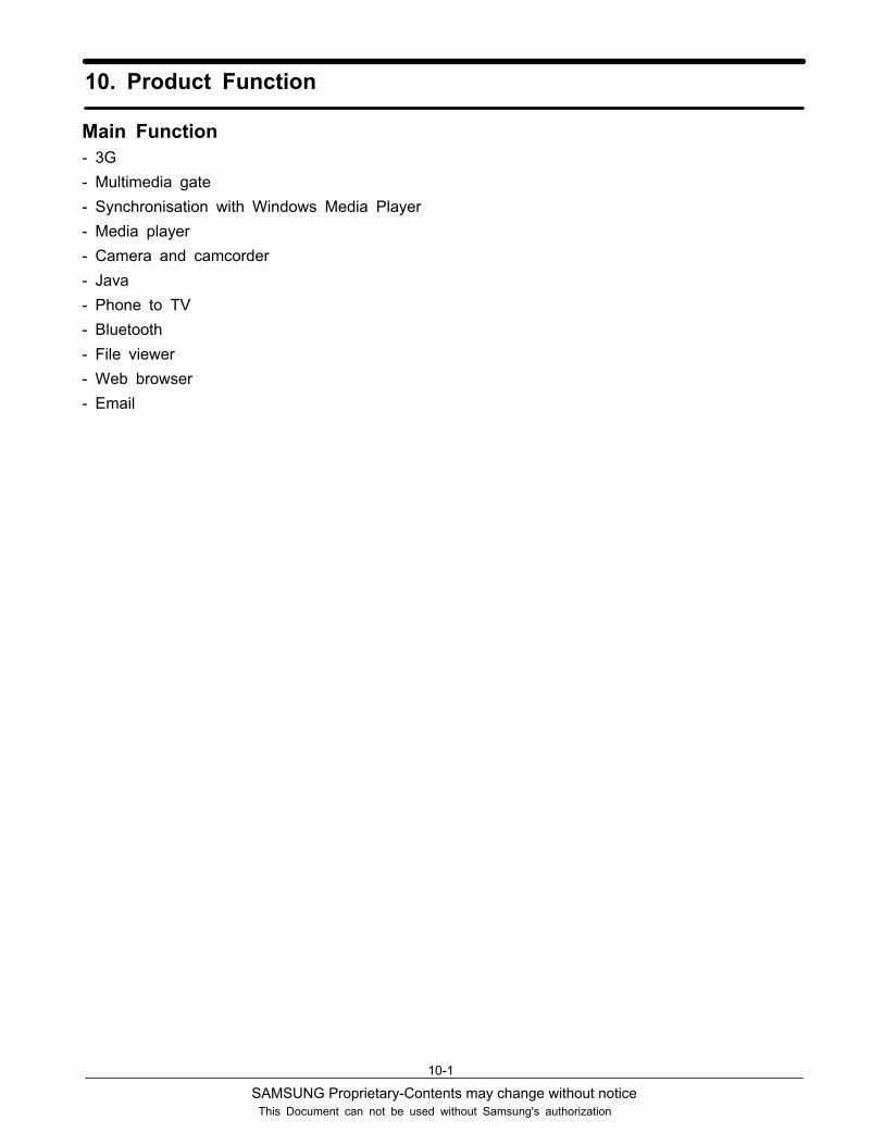
SAMSUNG Proprietary-Contents may change without notice
10. Product Function
10-1
This Document can not be used without Samsung's authorization
Main Function- 3G- Multimedia gate- Synchronisation with Windows Media Player- Media player- Camera and camcorder- Java- Phone to TV- Bluetooth- File viewer- Web browser- Email
This Service Manual is a property of Samsung Electronics Co.,Ltd.Any unauthorized use of Manual can be punished under applicableInternational and/or domestic law.
Samsung Electronics Co.,Ltd.
2007. 05. Rev.1.0
ⓒ
Country Web SiteNorth America service.samsungportal.comLatin America latin.samsungportal.comCIS cis.samsungportal.comEurope europe.samsungportal.comChina china.samsungportal.comAsia asia.samsungportal.comMideast & Africa mea.samsungportal.com
GSPN (Global Service Partner Network)