Room Temperature Total-Ionizing Dose Testing of Glenn ...
29
To be published on nepp.nasa.gov National Aeronautics and Space Administration Room Temperature Total-Ionizing Dose Testing of Glenn Research Center (GRC) 500 °C Durable 4H-SiC JFET IC Technology Kaitlyn Ryder, Jean-Marie Lauenstein, Ted Wilcox, and Marty Carts, NASA GSFC Philip Neudeck, Susan Wrbanek, and Robert Buttler, NASA GRC Liangyu Chen, Ohio Aerospace Institute, for NASA GRC Danny Spina, Jacobs Technology, for NASA GRC Prepared by: ____________________________ __________________________ Kaitlyn Ryder 7/24/2018 Pathways Intern Date
-
Upload
khangminh22 -
Category
Documents
-
view
0 -
download
0
Transcript of Room Temperature Total-Ionizing Dose Testing of Glenn ...

To be published on nepp.nasa.gov
National Aeronautics and Space Administration
Room Temperature Total-Ionizing Dose Testing of Glenn Research Center (GRC) 500 °C Durable 4H-SiC
JFET IC Technology
Kaitlyn Ryder, Jean-Marie Lauenstein, Ted Wilcox, and Marty Carts, NASA GSFC Philip Neudeck, Susan Wrbanek, and Robert Buttler, NASA GRC
Liangyu Chen, Ohio Aerospace Institute, for NASA GRC Danny Spina, Jacobs Technology, for NASA GRC
Prepared by: ____________________________ __________________________ Kaitlyn Ryder 7/24/2018 Pathways Intern Date

1 To be published on nepp.nasa.gov
1. Acronyms Used
AC: Alternating Current CMOS: Complementary Metal-Oxide-Semiconductor CTL: Control DUT: Device Under Test GRC: Glenn Research Center GSFC: Goddard Space Flight Center IC: Integrated Circuit I/O: Input/Output JFET: Junction Field Effect Transistor LLISSE: Long-Life Surface System Explorer REAG: Radiation Effects and Analysis Group (at NASA GSFC) SiC: Silicon Carbide SMU: Source-Measure Unit TID: Total Ionizing Dose
2. Introduction
The purpose of this testing was to obtain total ionizing dose (TID) information about custom-built research prototype silicon carbide (SiC) junction field effect transistor (JFET) integrated circuits (ICs) capable of prolonged operation in extremely high-temperature (500°C) environments. The circuits included ring oscillators and operational amplifiers as well as individual n-channel JFETs. This technology is being considered for use in high temperature, high pressure applications such as Long-Life Surface System Explorer (LLISSE). These devices were developed at NASA Glenn Research Center (GRC). Testing occurred from July 9th – July 13th, 2018.
3. Process and Integrated Circuit Description
The IC chips tested were diced from prototype research “Wafer 10.1” and “Wafer 10.2” fabricated at NASA GRC using “IC Version 10.1” process technology. The device technology is depicted in simplified cross section in Figure 1 below, and features n-type 4H-SiC epilayer-channel JFETs and resistors integrated with two levels of metal interconnect. Further information on the NASA GRC SiC JFET IC device technology, fabrication process, and demonstrated prolonged T ≥ 500 °C operational testing can be found in the following references:
[1] P. G. Neudeck, D. J. Spry, and L. Chen, Proc. IMAPS High Temperature Electronics Conf., 2016, pp. 263-271, available online at https://ntrs.nasa.gov/archive/nasa/casi.ntrs.nasa.gov/20160014879.pdf [2] P G. Neudeck, D. J. Spry, M. J. Krasowski, N. F. Prokop, G. M. Beheim, L. Chen, C. W. Chang, Proc. IMAPS Proc. IMAPS High Temperature Electronics Conf., 2018, pp. 71-78, available online at https://ntrs.nasa.gov/archive/nasa/casi.ntrs.nasa.gov/20180003391.pdf
The ICs are one of the first demonstrations of medium scale integration of 10s-100s SiC transistors capable of prolonged 500 °C operation. Much work has been done on improving the wafer fabrication and yields, while also addressing defects found in the metal interconnects due to temperature. These improvements will allow for more complex ICs to be implemented with this technology. Because the above reports note some significant changes in some device electrical properties as a function of radial distance from the center of the SiC wafer that the device was fabricated on, this radial distance is noted in Section 8 results tables. Ring oscillators provide in-package signal conditioning for capacitive pressure sensors. They take in a capacitive sensor input and output frequency modulated signals that allow for frequency-coded pressure measurements. These ring oscillators are 11 stages plus two output buffer stages and have 6 I/Os. They

2 To be published on nepp.nasa.gov
output an approximately 1 MHz, 100 mV triangular wave (as measured with non-negligible capacitive cable and probe loading effects). They are made of 28 JFETs. Operational amplifiers (op amps) are an analog building block that provides amplification of low level sensor signals. These op amps are 2-stage, differential input op amps with voltage gains of up to 50 possible with the on-chip resistors. The op amps are made up of 10 JFETs and can be used for piezoelectric sensors including SiC pressure sensors.
Figure 1. Simplified schematic cross section of SiC JFET and resistor device structure
with two levels of interconnect.
4. Test Samples
Six (6) n-channel JFETs (REAG ID #18-021), six (6) ring oscillators (ID#18-022), and six (6) operation amplifiers (ID #18-020) were provided for testing, for a total of eighteen (18) parts; one of each type of part was used as a control. Ring oscillator 5 was damaged during transport and measurements were not taken on it. All parts are version IC10.1 or IC10.2 (run 10, wafer 1 or 2) of the integrated circuit production. Table 1 lists relevant identification information. Parts are packaged in 12-pin cans whose schematic is shown in Figure 2.

3 To be published on nepp.nasa.gov
Figure 2: Schematic of 12-pin metal can package (Dimensions shown in inches).
Table 1: Device Identification Information
Device Name Serial Number Device Type Location (Figure 2)
A1 IC10.1pp0054-11: A1.10.20 Amplifier 1
A2 IC10.1pp0054-11: A6.07.05 Amplifier 14
A3 IC10.1pp0054-11: A3.13.11 Amplifier 8
A4 IC10.1pp0054-11: A4.13.14 Amplifier 12
A5 IC10.1pp0054-11: A5.22.17 Amplifier 6
A6 IC10.1pp0054-11: A2.10.17 Amplifier Control
O1 IC10.2pp0054-21: O1.12.17 Oscillator 10
O2 IC10.2pp0054-21: O2.12.20 Oscillator 2
O3 IC10.2pp0054-21: O6.18.08 Oscillator 15
O4 IC10.2pp0054-21: O4.15.20 Oscillator 4
O5 - Damaged IC10.2pp0054-21: O5.18.11 Oscillator 7
O6 IC10.2pp0054-21: O3.12.05 Oscillator Control
J1 IC10.1pp0054-11: J1.10.13 JFET 9
J2 IC10.1pp0054-11: J2.10.16 JFET 11
J3 IC10.1pp0054-11: J3.13.19 JFET 3
J4 IC10.1pp0054-11: J4.10.19 JFET 13
J5 IC10.1pp0054-11: J5.07.07 JFET 5
J6 IC10.1pp0054-11: J6.07.19 JFET Control

4 To be published on nepp.nasa.gov
5. Radiation Source and Dose Steps
Source: 60Co
Total Dose: 100, 200, 300, 500, 1000, 2000, 2500, 3000, 4100, 5000, 6171, and 7000 krad(Si)
Dose Rate: 152.3 krad(Si)/hr (daytime dose rate) 74.9 krad(Si)/hr (overnight dose rate)
6. Test Conditions and Measurements
Test Temperature: Room temperature
Bias Conditions (Figure 3):
JFETs: VDS=+25V, VSubstrate=-25V, VG=0V Oscillators: VDD=+25V, VSS=VSubstrate=-25V Amplifiers: VDD=+25V, VSS=VSubstrate=-25V, VIN=0V
Measurements: JFETs: IDSS, Ioff vs. dose; IV curves vs. dose Oscillators: Frequency, amplitude vs. dose Amplifiers: Voltage gain vs. dose, voltage offset vs. dose
Figure 3: Pinout block diagrams showing bias conditions during irradiation.
7. Test Methods
Samples to be irradiated were mounted on a custom test board (Figure 4) which was then positioned inside a PbAl box (Figure 5) in the radiation chamber. Test equipment (Table 2) was placed on a bench outside the chamber (Figure 6). The devices under test (DUTs) were connected to the test equipment via 50’ BNC cables using a Keithley 7001 switch box to enable individual DUT measurements between dose steps. Control devices were placed on an ESD mat near the test equipment and interfaced via clip leads. After the final dose step and measurement, control samples were mounted on the test board in the chamber and re-measured via the 50’ BNC leads. During irradiation, all parts were biased according to section 5 above (see also Table 3 below).

5 To be published on nepp.nasa.gov
Testing was performed by Kaitlyn Ryder (GSFC-561), Marty Carts (GSFC-561), Philip Neudeck (GRC-LCS), Susan Wrbanek (GRC-LCP), and Jean-Marie Lauenstein (GSFC-561). Irradiation began at 8:03 AM on July 10th, 2018 and lasted until 1:24 PM on July 13th, 2018. The test flow is given in Table 4. All samples underwent pre-rad characterization according to the tests listed in section 6 above. During irradiation, all parts were kept under bias per Figure 3. After each dose step, bias was maintained for an additional 15 minutes to allow for prompt annealing to occur before devices were again characterized. Because irradiation steps spanned 4 days, a reduced dose rate was necessary overnight. At the end of the radiation test campaign, samples and equipment were shipped back to NASA GRC, resulting in a two-week unbiased anneal during transport. Parts were then re-characterized at GRC over a period of approximately one week during which parts remained biased.
Table 2: Equipment List
Make Model Serial Number NASA ECN Date of Calibration Comments Test Fixture N/A N/A N/A N/A Custom
Agilent E3647A MY40003125 M641808 4/18/2018 Power supply (dual)
Tektronix TDS3014 B019090 M702299 6/11/2018 Oscilloscope Keithley 2410 1155279 M641619 5/30/2018 Source meter Keithley 2400 1155903 M641622 6/5/2018 Source meter Keithley 7001 N/A M702203 N/A Switch system Cables BNC N/A N/A N/A
Figure 4: Front-side image of test board.

6 To be published on nepp.nasa.gov
Figure 5: Test board with cabling, positioned in PbAl box.
Figure 6: Equipment stack outside cave, and control samples on ESD mat.

7 To be published on nepp.nasa.gov
Table 3: List of Connections on Test Board and Biases During Irradiation
Device Pin # Connection Voltage Bias During Irrad Equipment
Op Amp 1 GND BNC 0 V common ground 2 VDD BNC +25 V Agilent E3647A 3 VSS BNC -25 V Agilent E3647A 9 VSS BNC -25 V Agilent E3647A 10 OUT- BNC n/a Keithley 2400 lo 11 OUT+ BNC n/a Keithley 2400 hi 12 IN+ BNC 0 V Keithley 2410 hi Ring Oscillator 1 GND BNC 0 V common ground 2 VDD BNC +25 V Agilent E3647A 4 tied to 3 VSS BNC -25 V Agilent E3647A 7 VSS BNC -25 V Agilent E3647A 8 OUT BNC n/a Tektronix TDS3014 JFET 1 Source BNC 0 V common ground 2 Drain BNC +25 V Keithley 2410 hi 11 Substrate BNC -25 V Agilent E3647A 12 Gate BNC 0 V Keithley 2400 hi

8 To be published on nepp.nasa.gov
Table 4: Test Sequence
Date Run Irradiation Start Time
Irradiation Stop Time
Anneal Stop Time
Time Irradiated (hr:min:sec)
Dose Rate [krad(Si)/hr]
Total Dose Cumulative [krad(Si)]
Notes
7/9 0 -- -- -- 00:00:00 -- -- Arrive, unpack, set up, baseline measurements
7/10 0 7:00 -- 8:03 00:00:00 -- 0 Set up, pre-radiation measurements performed at 7:34. Ring oscillator 5 failed during transport, unresponsive.
7/10 1 08:03 08:42 08:57 00:39:18 152.6 100 7/10 2 09:19 09:58 10:14 00:39:18 152.6 200 7/10 3 10:35 11:14 11:30 00:39:18 152.6 300
7/10 4 11:51 13:01/13:22 13:37 01:18:42 152.6 500
A math error was made and irradiation was stopped prematurely. Devices annealed for 12 mins before irradiation continued to correct dose.
7/10 5 14:00 17:16 17:32 03:16:36 152.6 1000
7/10 6 18:47 08:08 08:23 13:20:33 74.9 2000
Overnight dose. Low dose rate dosimetry needed to be performed. 1.3 kR of dose was added to the parts unbiased during dosimetry.
7/11 7 08:52 12:08 12:24 03:16:36 152.6 2500 7/11 8 12:45 16:02 16:17 03:16:36 152.6 3000 7/11 9 17:00 07:40 07:56 14:40:40 74.9 4100 Overnight dose. 7/12 10 08:24 14:18 14:33 05:53:54 152.6 5000
7/12 11 15:15 07:15 07:31 15:37:36 74.9 6171
Overnight dose. Fire alarm caused shutter to close. Devices annealed for 23 mins and 9 sec while biased before radiation could be resumed. This was taken into account when calculating the total dose for this run.
7/13 12 07:58 13:24 13:40 05:25:56 152.6 7000

9 To be published on nepp.nasa.gov
8. Results
Ring Oscillators
The AC frequency and AC amplitudes of the oscillators were monitored during testing. Measurements were made after a 15-minute anneal period following each radiation step. Figures 7 and 8 show the frequency and amplitude as a function of total dose, respectively, and Tables 5 and 6 contain the raw data. In the tables, the DUT number is accompanied by the radial distance of the die from the center of the wafer, to within +/- 3 mm accuracy. Overall, the oscillators exhibited little change as a function of total dose, with both the AC frequency and AC amplitude remaining within 6% of the initial values for the test parts. The AC frequency increased after the first dose step (100 krad(Si)), then stabilized with no more than 1% variability upon subsequent dosing. The amplitude showed up to 5% (positive or negative) variability but with no trend with dose. O6, the unirradiated control part, on the other hand, demonstrated a large amount of variability, with the frequency dipping by as much as 14% and the amplitude by as much as 19%. Overall, this unirradiated control part showed a gradual decrease in amplitude over the series of measurements. The larger variability of the control part is most likely due to where and how the control part was set up. It was placed outside of the irradiation chamber on a test bench ESD mat with clip leads connecting its pins to the test equipment. The control part was subjected to more random mechanical vibrations than the test parts, which together with the less-secure clip-lead connections, most likely explains the variability in the measurements.
Figure 7: AC frequency measured in MHz as a function of total dose in krad(Si). Broken green line shows
contemporaneous measurements of the unirradiated control (ctl) part.

10 To be published on nepp.nasa.gov
Figure 8: AC amplitude measured in mV as a function of total dose in krad(Si). Broken green line shows contemporaneous measurements of the unirradiated control (ctl) part. Cable lengths differ between the
control and irradiated parts.
Table 5: Oscillator AC Frequency vs Dose AC Frequency (MHz)
Dose (krad(Si)) O1 12.4 mm
O2 21.2 mm
O3 21.2 mm
O4 21.8 mm
O6-Ctl 24.2 mm Mean Change Std Dev
0 1.15 1.07 1.08 1.09 1.00 0% 0% 100 1.20 1.12 1.14 1.14 0.99 4% 0% 200 1.20 1.12 1.14 1.14 1.00 4% 0% 300 1.20 1.12 1.14 1.14 1.00 4% 1% 500 1.20 1.12 1.14 1.14 1.01 4% 1%
1000 1.19 1.12 1.14 1.14 1.02 4% 1% 2000 1.19 1.13 1.14 1.14 1.01 5% 1% 2500 1.19 1.12 1.14 1.14 1.01 4% 1% 3000 1.19 1.12 1.14 1.14 1.02 4% 1% 4100 1.19 1.12 1.14 1.14 0.87 4% 1% 5000 1.18 1.12 1.15 1.14 0.99 4% 1% 6171 1.19 1.12 1.15 1.14 1.01 5% 1% 7000 1.18 1.12 1.15 1.14 1.02 4% 1%

11 To be published on nepp.nasa.gov
Table 6: Oscillator AC Amplitude vs Dose AC Amplitude (mV)
Dose (krad(Si)) O1 12.4 mm
O2 21.2 mm
O3 21.2 mm
O4 21.8 mm
O6-Ctl 24.2 mm Mean Change Std Dev
0 21.70 22.66 22.34 22.59 68.87 0% 0% 100 21.98 22.40 22.74 22.81 68.98 1% 1% 200 21.66 21.95 23.12 22.67 68.46 0% 3% 300 21.79 22.29 22.88 22.46 68.07 0% 2% 500 22.11 21.86 23.36 22.33 67.48 0% 4%
1000 22.10 22.10 23.42 22.99 67.71 1% 3% 2000 22.35 21.94 23.41 22.84 66.02 1% 3% 2500 22.56 22.00 23.07 23.23 65.44 2% 3% 3000 22.59 22.28 23.04 23.22 65.06 2% 3% 4100 22.50 21.89 23.03 22.67 55.90 1% 3% 5000 22.00 22.17 23.41 22.94 58.95 1% 3% 6171 22.45 22.26 23.46 22.68 62.36 2% 3% 7000 22.64 21.79 23.12 22.66 62.25 1% 4%
Operational Amplifiers
The DC gain and offset voltage of the amplifiers were monitored during testing. Measurements were made after a 15-minute anneal period following each radiation step. Figures 9 and 10 show the gain and offset voltage as a function of total dose, respectively, and Tables 7 and 8 contain the raw data. In the tables, the DUT number is accompanied by the radial distance of the die from the center of the wafer, to within +/- 3 mm accuracy. Overall, the amplifiers exhibited little change as a function of total dose. The gain in DUTs A1 and A2 increased slightly at the beginning of irradiation, decreased, and then saturated as dose continued to increase; the gain of the other DUTs only decreased with dose. For these latter DUTs, an initial increase in gain may have occurred prior to the overall decrease measured at the first dose step of 100 krad(Si). The initial gain increase followed by decrease suggests competing mechanisms where negative charge traps and positive charge traps are formed at different rates. By 1 Mrad(Si), the gain of all DUTs had dropped below pre-rad levels. The variability in the gain of the test parts remained within 21% of the initial values, whereas the variability of the unirradiated control part remained within 1% of the initial value. Annealing at room temperature (2 weeks unbiased during shipping from GSFC to GRC; 1 week biased at GRC) had little impact, and in some cases (A1, A2), resulted in a further decrease in gain (see open symbols in Figure 8). The offset voltage was minimally affected by dose. The different DUTs showed different trends in offset voltage with dose, such that some parts showed a slightly decreasing offset voltage trend and others showing minimal change or increasing offset voltage with dose. The variability of the test parts remaining within 9% of the initial values. The variability of the control part was much greater. The control part’s offset voltage continued to decrease with each measurement, down to almost 50% of its original value. The control part’s offset voltage was more than an order of magnitude lower than that of the test parts, however, so that the magnitude of change was the lowest of all the parts. Change in gain was no indication of the trend in offset voltage; for example, DUT A2 exhibited an 11% decrease it its gain, but no significant change to its offset voltage. There was no obvious correlation of either gain or offset voltage response with die location on the wafer.

12 To be published on nepp.nasa.gov
The output voltage and gain vs input voltage curves were monitored. Figures 11 – 16 show these for each of the 6 amplifiers; for clarity, only curves at select dose steps are shown. Note the ordinate axis varies between figures. Looking at the test parts in Figures 11 – 15 reveals some general trends. As expected from the data in Tables 7 and 8, there is a slight stretching in the output voltage curves and a decrease in the gain curves. There is part-part variability in whether the gain curves narrow or widen with dose. The unirradiated control part data in Figure 16 demonstrates the effect of the 50’ coaxial cables used to address the test devices: the blue broken line in the plots is from measurements made with the control part placed on the test board in the chamber.
Figure 9: Amplifier DC gain as a function of total dose in krad(Si). Broken green line shows
contemporaneous measurements of the unirradiated control (ctl) part.
Figure 10: Amplifier Offset voltage measured in mV as a function of total dose in krad(Si). Broken green line
shows contemporaneous measurements of the unirradiated control (ctl) part.

13 To be published on nepp.nasa.gov
Table 7: Amplifier DC Gain vs Dose DC Gain
Dose (krad(Si)) A1 22.8 mm
A2 30.0 mm
A3 6.0 mm
A4 3.0 mm
A5 29.5 mm
A6-Ctl 15.0 mm Mean Change Std Dev
0 23.7 50.3 40.4 45.3 39.0 57.7 0% 0% 100 27.0 51.3 39.5 44.3 39.0 57.8 2% 7% 200 26.4 51.2 39.4 43.9 38.9 57.9 1% 6% 300 25.8 50.7 39.6 43.5 38.7 57.8 1% 5% 500 25.4 50.1 38.7 42.9 38.2 57.9 -1% 5%
1000 23.4 48.5 38.0 42.4 37.5 58.0 -4% 2% 2000 21.2 46.5 37.6 42.1 36.9 58.1 -8% 2% 2500 20.7 46.1 37.6 42.0 36.7 58.1 -8% 3% 3000 20.3 45.7 37.3 42.1 36.6 58.2 -9% 3% 4100 19.4 45.3 37.4 42.1 36.7 58.3 -10% 5% 5000 19.2 45.1 37.3 41.9 33.5 58.3 -12% 5% 6171 18.7 44.8 37.4 42.0 35.9 58.4 -11% 6% 7000 18.6 44.7 37.3 41.8 35.4 58.5 -11% 6%
Post in-chamber -- -- -- -- -- 40.49 2 wk anneal 16.3 44.0 38.3 42.5 36.0 -- -13% 11%
Table 8: Amplifier Offset Voltage vs Dose Offset Voltage (mV)
Dose (krad(Si)) A1 22.8 mm
A2 30.0 mm
A3 6.0 mm
A4 3.0 mm
A5 29.5 mm
A6-Ctl 15.0 mm Mean Change Std Dev
0 358.8 438.3 204.5 257.4 396.5 13.7 0% 0% 100 355.1 442.1 204.4 255.0 410.3 14.2 0% 2% 200 350.8 440.7 200.7 252.7 410.1 14.2 0% 2% 300 348.5 437.9 195.8 254.1 409.6 14.5 -1% 3% 500 343.4 431.9 192.0 248.1 408.9 14.2 -2% 4%
1000 337.2 433.8 189.7 246.0 409.0 13.8 -3% 4% 2000 335.9 435.3 186.4 249.1 412.0 10.9 -3% 5% 2500 338.1 435.5 189.2 252.7 414.0 9.8 -2% 5% 3000 339.4 436.8 190.2 255.2 414.6 9.8 -2% 5% 4100 338.6 436.7 191.9 255.0 415.0 8.4 -2% 4% 5000 341.2 437.1 195.5 256.2 419.6 8.1 -1% 4% 6171 340.9 438.6 197.2 257.5 417.2 7.2 -1% 4% 7000 342.2 439.7 199.4 259.1 419.2 7.0 0% 4%
Post in-chamber -- -- -- -- -- 3.1 2 wk anneal 318.1 436.9 192.5 251.9 424.7 -- -3% 7%

14 To be published on nepp.nasa.gov
Figure 11: Input vs output voltage (left) and vs gain (right) of A1 as a function of total dose, for selected
doses.
.
Figure 12: Input vs output voltage (left) and input voltage vs gain (right) of A2 as a function of total dose,
for selected doses. Note ordinate scales differ from Figure 11.
Figure 13: Input vs output voltage (left) and input voltage vs gain (right) of A3 as a function of total dose, for
selected doses. Note ordinate scales differ from Figure 11.

15 To be published on nepp.nasa.gov
Figure 14: Input vs output voltage (left) and input voltage vs gain (right) of A4 as a function of total dose, for
selected doses. Note ordinate scales differ from Figure 11.
Figure 15: Input vs output voltage (left) and input voltage vs gain (right) of A5 as a function of total dose, for
selected doses. Note ordinate scales differ from Figures 11-14.
Figure 16: Input vs output voltage (left) and input voltage vs gain (right) of unirradiated control part, A6, as a function of total dose, for selected doses. Note ordinate scales differ from Figures 11-15. Blue broken lines
are measurements taken with the control part placed in the test board to account for 50’ cable lengths.

16 To be published on nepp.nasa.gov
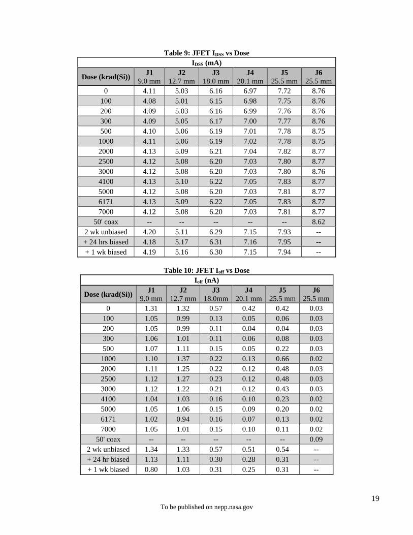
JFETs The drain current (ID) vs gate voltage (VGS) and ID vs drain voltage (VDS) curves were monitored during testing at constant substrate bias VSubstrate = -25 V. Measurements were made after a 15-minute anneal period following each radiation step. Curves were again measured at NASA GRC following a two-week unbiased anneal during shipping from GSFC, after 24 hours under bias at GRC, and finally after 1 week under bias. From these curves the shorted-gate drain current (IDSS), off-state gate leakage current (Ioff), pinch-off voltage (Vp), and transconductance at VGS = 0 V (gm0) could be found. IDSS is defined as ID when VGS equals 0 V and VDS equals 25 V, and Ioff is defined as ID when VGS equals -12 V and VDS equals 20 V. Pinch-off voltage was extrapolated for ID = 0 A using ID = IDSS*(1- VGS/Vp)2. In addition, VGS at ID = 15 nA and VDS = 20 V was interpolated to quantify the subthreshold shift in the ID vs. VGS curves as a function of dose. Figure 16 shows the change in IDSS as a function of dose; Table 8 provides actual IDSS values. Figure 18 and Table 10 show Ioff as a function of total dose. The change in pinch-off voltage as a function of dose is plotted in Figure 19, with actual values given in Table 11. Figure 20 and Table 12 show the impact of dose on VGS at ID = 15 nA. Finally, gm0 values are given in Table 13. In the tables, the DUT number is accompanied by the radial distance of the die from the center of the wafer, to within +/- 3 mm accuracy. There was no obvious correlation between JFET performance and this radial distance on the wafer. Overall, the change the JFETs saw as a function of total dose was minimal. The change in IDSS was within ±1.5% of the initial values, with a general trend toward increasing values (note that DUT J1 showed initially decreasing IDSS before the current rose above pre-rad levels). Ioff varied by as much as 91%, with the control part fluctuating by as much as 50%, demonstrating that measurement precision contributed to this variability. Transconductance remained unchanged. Pinch-off voltage showed a small increase with dose but the change remained within 2%. Most of the increase in pinch-off voltage occurred below 1 Mrad(Si). The most notable change occurred in the subthreshold region of the ID vs. VGS curves, where a subthreshold “hump” developed. This signature suggests charge trapping effects in the oxide, likely lessening the depletion of the channel region along the termination of the gate width due to excess positive charge buildup. The interface of the oxide and SiC material typically has a high concentration of traps – possible negative charge trapping at the interface could mitigate much of the positive trapped charge in the bulk of the oxide, resulting in the minimal overall effects of dose to the JFETs. Note that after remaining unbiased for two weeks, the subthreshold “hump” disappeared, re-emerging in subsequent measurements after JFETs remained under bias (see Table 12 and Figures 21 – 25). Figures 21 – 26 show ID vs VGS and VDS for each of the 6 JFETs at VSubstrate = -25V. ID vs VGS was measured at a VDS of 20 V, and ID vs VDS was measured at VGS of 0 V, -2 V, -4 V, -6 V, -8 V, and -10 V. Starting with the unirradiated control part in Figure 26, the ID vs VGS and VDS curves remain nearly constant throughout the testing. This is true even when the control part is placed on the test board. Changes in the IV curves of the test parts are thus due to radiation exposure. Examining the ID vs VGS curves for the test devices shows that in all parts a negative shift in VGS occurred at subthreshold values of drain current (this effect is quantified in Table 12 for ID = 15 nA). The change in Ioff is also easily seen from the ID vs VGS curves and is most prevalent in J3, J4, and J5. As expected from the ID VS VGS curves, ID vs VDS showed the most change as a function of dose at the lower VGS values, excluding VGS equals -10 V; at VGS equals -10 V, the signal appears to be mostly noise and is therefore not shown (with the exception of the control part, J6, whose pinch-off voltage was less than -10 V).

17 To be published on nepp.nasa.gov
Figure 17. Percent change in IDSS as a function of dose measured in krad(Si).
Unirradiated control device is J6, shown in green broken line.
Figure 18. Ioff measured in nA as a function of total dose in krad(Si).
Unirradiated control device is J6, shown in green broken line.

18 To be published on nepp.nasa.gov
Figure 19. Percent change in VP as a function of dose measured in krad(Si).
Unirradiated control device is J6, shown in green broken line.
Figure 20. VGS at ID = 15 nA (VDS = 20 V) as a function of dose measured in krad(Si).
Unirradiated control device is J6, shown in green broken line.
19 To be published on nepp.nasa.gov
Table 9: JFET IDSS vs Dose IDSS (mA)
Dose (krad(Si)) J1 9.0 mm
J2 12.7 mm
J3 18.0 mm
J4 20.1 mm
J5 25.5 mm
J6 25.5 mm
0 4.11 5.03 6.16 6.97 7.72 8.76 100 4.08 5.01 6.15 6.98 7.75 8.76 200 4.09 5.03 6.16 6.99 7.76 8.76 300 4.09 5.05 6.17 7.00 7.77 8.76 500 4.10 5.06 6.19 7.01 7.78 8.75
1000 4.11 5.06 6.19 7.02 7.78 8.75 2000 4.13 5.09 6.21 7.04 7.82 8.77 2500 4.12 5.08 6.20 7.03 7.80 8.77 3000 4.12 5.08 6.20 7.03 7.80 8.76 4100 4.13 5.10 6.22 7.05 7.83 8.77 5000 4.12 5.08 6.20 7.03 7.81 8.77 6171 4.13 5.09 6.22 7.05 7.83 8.77 7000 4.12 5.08 6.20 7.03 7.81 8.77
50' coax -- -- -- -- -- 8.62 2 wk unbiased 4.20 5.11 6.29 7.15 7.93 -- + 24 hrs biased 4.18 5.17 6.31 7.16 7.95 -- + 1 wk biased 4.19 5.16 6.30 7.15 7.94 --
Table 10: JFET Ioff vs Dose
Ioff (nA)
Dose (krad(Si)) J1 9.0 mm
J2 12.7 mm
J3 18.0mm
J4 20.1 mm
J5 25.5 mm
J6 25.5 mm
0 1.31 1.32 0.57 0.42 0.42 0.03 100 1.05 0.99 0.13 0.05 0.06 0.03 200 1.05 0.99 0.11 0.04 0.04 0.03 300 1.06 1.01 0.11 0.06 0.08 0.03 500 1.07 1.11 0.15 0.05 0.22 0.03
1000 1.10 1.37 0.22 0.13 0.66 0.02 2000 1.11 1.25 0.22 0.12 0.48 0.03 2500 1.12 1.27 0.23 0.12 0.48 0.03 3000 1.12 1.22 0.21 0.12 0.43 0.03 4100 1.04 1.03 0.16 0.10 0.23 0.02 5000 1.05 1.06 0.15 0.09 0.20 0.02 6171 1.02 0.94 0.16 0.07 0.13 0.02 7000 1.05 1.01 0.15 0.10 0.11 0.02
50' coax -- -- -- -- -- 0.09 2 wk unbiased 1.34 1.33 0.57 0.51 0.54 -- + 24 hr biased 1.13 1.11 0.30 0.28 0.31 -- + 1 wk biased 0.80 1.03 0.31 0.25 0.31 --

20 To be published on nepp.nasa.gov
Table 11: JFET Pinch-Off Voltage vs Dose Vp (V)
Dose (krad(Si)) J1 9.0 mm
J2 12.7 mm
J3 18.0 mm
J4 20.1 mm
J5 25.5 mm
J6 25.5 mm
0 -7.10 -7.65 -8.90 -9.20 -9.18 -10.98 100 -7.18 -7.73 -8.98 -9.28 -9.25 -10.98 200 -7.19 -7.75 -8.98 -9.29 -9.26 -10.98 300 -7.19 -7.76 -8.99 -9.29 -9.26 -10.98 500 -7.20 -7.78 -9.01 -9.30 -9.27 -10.98
1000 -7.23 -7.80 -9.02 -9.31 -9.28 -10.98 2000 -7.23 -7.80 -9.02 -9.32 -9.29 -10.99 2500 -7.24 -7.80 -9.03 -9.32 -9.29 -10.99 3000 -7.24 -7.80 -9.03 -9.32 -9.29 -10.99 4100 -7.23 -7.80 -9.02 -9.32 -9.29 -10.99 5000 -7.23 -7.81 -9.03 -9.33 -9.30 -10.99 6171 -7.23 -7.79 -9.02 -9.32 -9.30 -10.99 7000 -7.23 -7.81 -9.03 -9.33 -9.31 -10.99
50' coax -- -- -- -- -- -11.02 2 wk unbiased -7.14 -7.64 -8.94 -9.25 -9.24 -- + 24 hr biased -7.19 -7.74 -8.97 -9.28 -9.27 -- + 1 wk biased -7.20 -7.74 -8.97 -9.28 -9.27 --
Table 12: JFET VGS at ID = 15 nA (VDS = 20 V) vs Dose VGS at ID = 15 nA
Dose (krad(Si)) J1 9.0 mm
J2 12.7 mm
J3 18.0 mm
J4 20.1 mm
J5 25.5 mm
J6 25.5 mm
0 -7.25 -7.74 -8.75 -8.93 -8.49 -10.74 100 -7.50 -7.99 -9.00 -9.00 -8.70 -10.74 200 -7.50 -8.00 -9.00 -9.25 -8.75 -10.74 300 -7.74 -8.23 -9.26 -9.25 -8.93 -10.74 500 -7.75 -8.25 -9.25 -9.50 -8.99 -10.74
1000 -8.00 -8.49 -9.51 -9.75 -9.19 -10.74 2000 -8.15 -8.49 -9.50 -9.75 -9.18 -10.74 2500 -8.14 -8.50 -9.50 -9.75 -9.21 -10.74 3000 -8.20 -8.50 -9.50 -9.75 -9.21 -10.74 4100 -8.00 -8.49 -9.50 -9.75 -9.19 -10.74 5000 -8.00 -8.50 -9.50 -9.75 -9.21 -10.74 6171 -8.00 -8.49 -9.50 -9.75 -9.19 -10.74 7000 -8.00 -8.50 -9.50 -9.75 -9.21 -10.74
50' coax -- -- -- -- -- -10.74 2 wk unbiased -7.25 -7.50 -8.50 -8.75 -8.61 -- + 24 hr biased -7.75 -7.77 -8.76 -9.03 -8.88 -- + 1 wk biased -7.68 -7.77 -8.77 -9.04 -8.91 --

21 To be published on nepp.nasa.gov
Table 13: Transconductance at VGS = 0 V vs Dose gm0
Dose (krad(Si)) J1 9.0 mm
J2 12.7 mm
J3 18.0 mm
J4 20.1 mm
J5 25.5 mm
J6 25.5 mm
0 1.07 1.22 1.29 1.40 1.52 1.49 100 1.06 1.21 1.28 1.40 1.52 1.48 200 1.06 1.21 1.28 1.40 1.52 1.48 300 1.06 1.21 1.28 1.40 1.52 1.48 500 1.06 1.21 1.28 1.40 1.52 1.48
1000 1.06 1.21 1.27 1.39 1.52 1.48 2000 1.06 1.21 1.28 1.40 1.52 1.48 2500 1.06 1.21 1.27 1.39 1.52 1.48 3000 1.06 1.21 1.27 1.39 1.52 1.48 4100 1.06 1.21 1.28 1.40 1.52 1.48 5000 1.06 1.21 1.28 1.39 1.52 1.48 6171 1.06 1.21 1.28 1.40 1.52 1.48 7000 1.06 1.21 1.28 1.39 1.52 1.48
50' coax -- -- -- -- -- 1.46 2 wk unbiased 1.09 1.24 1.31 1.43 1.55 -- + 24 hr biased 1.08 1.24 1.31 1.43 1.55 -- + 1 wk biased 1.08 1.24 1.30 1.43 1.55 --

22 To be published on nepp.nasa.gov
Figure 21. ID vs VGS and ID vs VDS for J1.

23 To be published on nepp.nasa.gov
Figure 22. ID vs VGS and ID vs VDS for J2.

24 To be published on nepp.nasa.gov
Figure 23. ID vs VGS and ID vs VDS for J3.

25 To be published on nepp.nasa.gov
Figure 24. ID vs VGS and ID vs VDS for J4.

26 To be published on nepp.nasa.gov
Figure 25. ID vs VGS and ID vs VDS for J5.

27 To be published on nepp.nasa.gov
Figure 26. ID vs VGS and ID vs VDS for unirradiated control J6.

28 To be published on nepp.nasa.gov
10. Summary
Total ionizing dose (TID) testing of custom-built research prototype silicon carbide (SiC) junction field effect transistor (JFET) integrated circuits (ICs) capable of prolonged operation in extremely high-temperature (500°C) environments was conducted using a 60Co source. The circuits included ring oscillators and operational amplifiers as well as individual n-channel JFETs, and were irradiated in steps up to 7 Mrad(Si). Overall, devices remained operational and exhibited minimal change as a result of this high level of total ionizing dose. This technology is therefore promising for extreme environments such as that of Jupiter, where 7 Mrad(Si) would be expected (with 2x design margin) outside of a high-mass “vault”, within standard 100-mil Al electronics box walls instead. The test results are in keeping with expected performance of JFET-based technologies due to the absence of gate or isolation oxides and due to being a majority carrier device. It is difficult to make direct comparisons with silicon technology, however, because silicon integrated circuits are most often CMOS (for digital circuits) or bipolar/biCMOS (for linear/analog circuits). When radiation hardened, some silicon circuits can be expected to operate at doses up to 1 Mrad(Si) or greater (CMOS), although for op amps and other linear bipolar/biCMOS technologies, performance would be expected to significantly degrade at much lower doses. Most silicon JFETs are used as pre-amplifiers and are therefore characterized for noise as a function of radiation exposure, as opposed to overall parametric performance. As this SiC JFET IC technology matures and devices are designed with more demanding performance criteria, greater sensitivity of some parameters to TID exposure would be expected. Characterization of noise and/or JFET gate leakage current, for example would be recommended for discrete JFETs used as pre-amplifiers. For precision op amps, bias current and offset current are additional parameters to monitor for possible degradation. 11. Acknowledgement
Funding for this work was provided by the Planetary Exploration Science Technology Office (PESTO), Planetary Science Division, NASA Headquarters, with supplemental support by the NASA Electronic Parts and Packaging program. SiC IC fabrication and packaging was performed at NASA GRC under joint funding from the NASA Science Mission Directorate and the NASA Aeronautics Directorate. G. W. Hunter, W. T. John and F. Lam at NASA GRC were also instrumental to the work carried out at NASA GRC.