Robust Solid State Quantum System Operating at 800 K - arXiv
9
Robust Solid State Quantum System Operating at 800 K Mehran Kianinia, Sherif Abdulkader Tawfik, Blake Regan, Toan Trong Tran, Michael J. Ford, Igor Aharonovich, * and Milos Toth ^ † School of Mathematical and Physical Sciences, University of Technology Sydney, Ultimo, NSW, 2007, Australia. KEYWORDS: Single photon source, high temperature photoluminescence ABSTRACT: Realization of Quantum information and communications technologies requires robust, stable solid state single photon sources. However, most existing sources cease to function above cryogenic or room temperature due to thermal ionization or strong phonon coupling which impede their emissive and quantum properties. Here we present an efficient single photon source based on a defect in a van der Waals crystal that is optically stable and operates at elevated temperatures of up to 800 K. The quantum nature of the source and the photon purity are maintained upon heating to 800 K and cooling back to room temperature. Our report of a robust high temperature solid state single photon source constitutes a significant step towards practical, integrated quantum technologies for real-world environments. Keywords: high temperature nanophotonics, quantum emitters, 2D materials INTRODUCTION Modern light-based technologies require so- phisticated materials growth and device engineer- ing techniques to achieve optimum performance under ambient conditions. Optically active defects in solids are a vital part of numerous such technol- ogies spanning light emitting diodes (LEDs) 1, 2 , la- sers 3 , sensors 4, 5 and communications 6 . An emerg- ing application of localized individual defects is their use as single photon sources (SPSs) in inte- grated nanophotonics and quantum information processing schemes that utilize individual photons as information carriers 7, 8, 9, 10 . For such applica- tions to become a reality there is an urgent need for robust, on-demand SPSs. Furthermore, these sources should be optically active in harsh envi- ronments and at elevated temperatures that are typical of high density integrated circuits. Hence, over the last decade, research into solid state SPSs – quantum dots (QDs) and color centers – has accelerated dramatically. Quantum dots mostly operate only at cryogenic temperatures be- cause of low carrier binding energies and thermal ionization at elevated temperatures 11, 12 . On the other hand, color centers in solids (defects and im- purities, also known as artificial atoms) often have deep electronic states that enable SPS operation near room temperature (RT) 13, 14, 15 . However, both QDs and color centers typically suffer from effi- cient coupling between electrons and lattice pho- nons that results in an overall reduction of bright- ness at higher temperatures. In this work, we report a solid state SPS that operates at temperatures as high as 800 K. The SPS maintains its quantum nature during a high temperature thermal cycle – that is, the photon pu- rity (defined as the fraction of single photon emis- sion events) does not decrease upon heating, and the SPS optical properties are preserved after heat- ing up to 800 K and cooling back to room temper- ature, as would be required for practical on-chip devices. The SPS is a deep trap defect in layered hexagonal boron nitride (hBN) – a van der Waals crystal with a wide indirect bandgap of ~ 6 eV 16 and favorable thermal, chemical and mechanical properties 17, 18 . The recently-discovered SPSs in hBN are extremely bright, chemically stable, fully polarized, and exhibit a broad range of emission colors 19, 20, 21, 22, 23, 24, 25 . Given the two dimensional (2D), layered nature of hBN and the extreme ther- mal stability of the SPSs demonstrated here, fabri- cation of hybrid photonic systems is a promising potential path to high density integrated circuits designed to withstand heating that occurs during operation at RT. MATERIALS AND METHODS
-
Upload
khangminh22 -
Category
Documents
-
view
8 -
download
0
Transcript of Robust Solid State Quantum System Operating at 800 K - arXiv
Robust Solid State Quantum System Operating at 800 K Mehran Kianinia, Sherif Abdulkader Tawfik, Blake Regan, Toan Trong Tran, Michael J. Ford, Igor Aharonovich, * and Milos Toth^ † School of Mathematical and Physical Sciences, University of Technology Sydney, Ultimo, NSW, 2007, Australia. KEYWORDS: Single photon source, high temperature photoluminescence
ABSTRACT: Realization of Quantum information and communications technologies requires robust, stable solid state single photon sources. However, most existing sources cease to function above cryogenic or room temperature due to thermal ionization or strong phonon coupling which impede their emissive and quantum properties. Here we present an efficient single photon source based on a defect in a van der Waals crystal that is optically stable and operates at elevated temperatures of up to 800 K. The quantum nature of the source and the photon purity are maintained upon heating to 800 K and cooling back to room temperature. Our report of a robust high temperature solid state single photon source constitutes a significant step towards practical, integrated quantum technologies for real-world environments.
Keywords: high temperature nanophotonics, quantum emitters, 2D materials
INTRODUCTION
Modern light-based technologies require so-phisticated materials growth and device engineer-ing techniques to achieve optimum performance under ambient conditions. Optically active defects in solids are a vital part of numerous such technol-ogies spanning light emitting diodes (LEDs)1, 2, la-sers3, sensors4, 5 and communications6. An emerg-ing application of localized individual defects is their use as single photon sources (SPSs) in inte-grated nanophotonics and quantum information processing schemes that utilize individual photons as information carriers7, 8, 9, 10. For such applica-tions to become a reality there is an urgent need for robust, on-demand SPSs. Furthermore, these sources should be optically active in harsh envi-ronments and at elevated temperatures that are typical of high density integrated circuits.
Hence, over the last decade, research into solid state SPSs – quantum dots (QDs) and color centers – has accelerated dramatically. Quantum dots mostly operate only at cryogenic temperatures be-cause of low carrier binding energies and thermal ionization at elevated temperatures11, 12. On the other hand, color centers in solids (defects and im-purities, also known as artificial atoms) often have deep electronic states that enable SPS operation near room temperature (RT)13, 14, 15. However, both
QDs and color centers typically suffer from effi-cient coupling between electrons and lattice pho-nons that results in an overall reduction of bright-ness at higher temperatures.
In this work, we report a solid state SPS that operates at temperatures as high as 800 K. The SPS maintains its quantum nature during a high temperature thermal cycle – that is, the photon pu-rity (defined as the fraction of single photon emis-sion events) does not decrease upon heating, and the SPS optical properties are preserved after heat-ing up to 800 K and cooling back to room temper-ature, as would be required for practical on-chip devices. The SPS is a deep trap defect in layered hexagonal boron nitride (hBN) – a van der Waals crystal with a wide indirect bandgap of ~ 6 eV16 and favorable thermal, chemical and mechanical properties17, 18. The recently-discovered SPSs in hBN are extremely bright, chemically stable, fully polarized, and exhibit a broad range of emission colors19, 20, 21, 22, 23, 24, 25. Given the two dimensional (2D), layered nature of hBN and the extreme ther-mal stability of the SPSs demonstrated here, fabri-cation of hybrid photonic systems is a promising potential path to high density integrated circuits designed to withstand heating that occurs during operation at RT.
MATERIALS AND METHODS
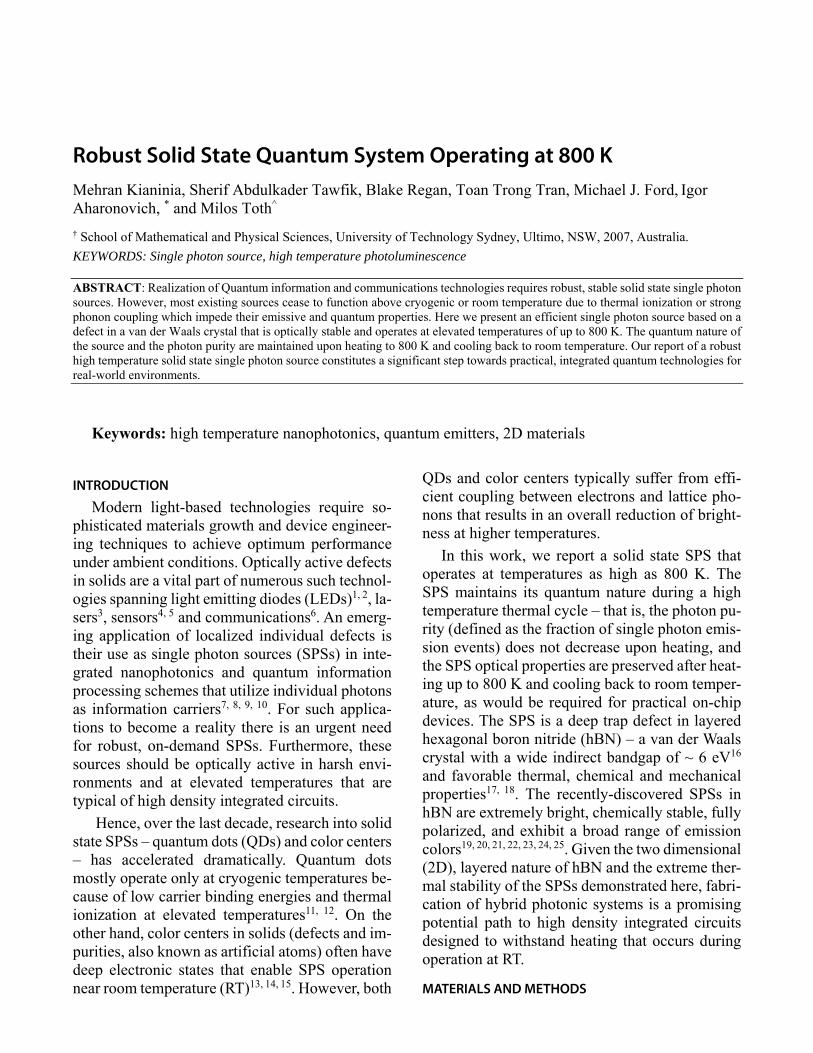
A schematic illustration of hBN on a hot sub-strate is shown in figure 1a. The sample consists of a few-layer flake of atomically thin hBN bonded by van der Waals forces. The hBN flakes (Graphene Supermarket) were dropcast onto a sil-icon wafer and annealed in a tube furnace at 850 °C for 30 minutes under 1 Torr of Argon to acti-vate the SPSs19. To perform the heating experi-ments, we use a purpose-built vacuum chamber with a thin quartz window and a long working dis-tance, high numerical aperture (0.7) objective, shown in figure 1b. The samples were mounted on a pyrolitic boron nitride heater, and the tempera-ture was measured using a thermocouple fixed to the silicon substrate. A turbo molecular pump was
used to achieve a base pressure of ~1×10⁻⁶ mBar, and a 532 nm laser was used as the excitation source in the confocal photoluminescence setup. For all measurements except time-resolved photo-luminescence, the laser power was fixed at 3 mW (measured before the window of the chamber). The collected light was filtered using a 532 nm di-chroic mirror and an additional long pass filter. The collected light was sent either to a spectrome-ter (Acton Spectra ProTM, Princeton Instrument Inc.) equipped with a 300 lines/mm grating and a charged-coupled device (CCD) detector with a resolution of 0.14 nm or to a Hanbury Brown and Twiss set-up for single photon correlation meas-urement (figure 1c).
Figure 1. (a) Schematic illustration of a hBN crystal hosting a single photon source atop of a heated substrate. (b) The purpose-built vacuum chamber setup used in this study. (c) Hanbury Brown and Twiss set-up equipped with vacuum chamber used in this study. Band pass filter according to ZPL energy of the SPS was used only for conscience measurements. (d) Room temperature PL spectra acquired from two representative SPSs in hBN. The shaded areas represent the filtered regions used to record the correlation measurements. (e) Antibunching behavior of the sources demonstrated by autocorrelation functions with g2(0) values of 0.24 and 0.37 for SPS #1 (blue) and SPS #2 (red), respectively, confirming the quantum nature of the emissions. The g2() from SPS #2 was offset for clarity. The data were fitted with a three level system (solid curves).

The emitted light was coupled to an optical fi-ber and split to two paths into avalanche photodi-odes in order to perform correlation measurements using a time correlated single photon counting module (Picoharp300TM, PicoQuantTM). Life-time measurements were done with a 510 nm pulsed laser excitation source at 30 µw power with a 100 ps pulse width and 10 MHz repetition rate.
RESULTS AND DISCUSSION
Two SPSs in different hBN crystals were stud-ied in this work. Figure 1c shows RT photolumi-nescence (PL) spectra recorded from the SPSs. The spectrum from SPS #1 consists of two peaks at ~1.94 eV and ~1.78 eV attributed to the zero phonon line (ZPL) and the phonon side band (PSB), respectively19. SPS #2 has a sharper ZPL
centered at ~1.75 eV, and a negligible PSB (the emissions beyond ~1.8 eV are background). These particular two emitters were selected for the pre-sent study because their spectra are representative of the emission spectrum diversity that has been observed previously in hBN19 (in terms of ZPL width and position, and PSB intensity).
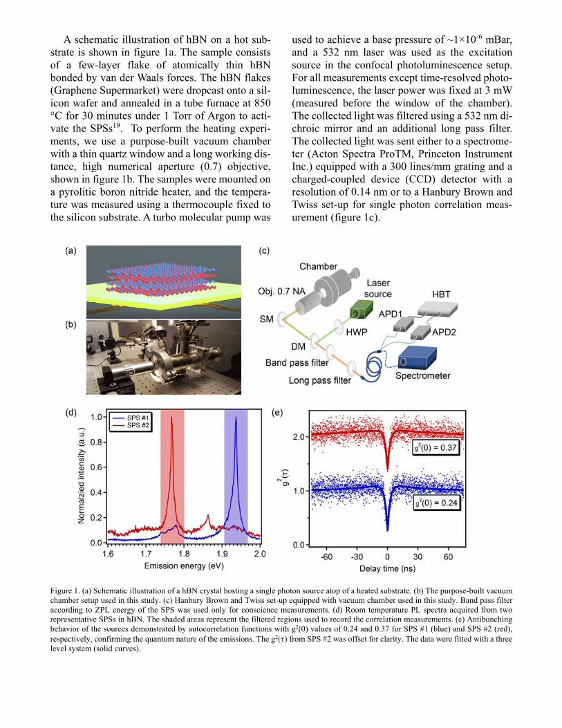
After we identified reliable SPSs, we pro-ceeded to the heating experiment. The tempera-ture-dependence of each SPS was characterized by measuring its photophysical properties at 100 K increments during a 300 K – 800 K – 300 K ther-mal cycle. Figure 2a, b and figure 2c, d show au-tocorrelation functions and normalized PL spectra obtained from SPS #1 (blue data set) and SPS #2 (red data set) obtained during the heating phase of the thermal cycle, respectively.
Figure 2. Temperature dependence of the quantum emission and photoluminescence of SPSs in hBN during heating. (a) Autocorrelation curve and (b) normalized PL spectrum measured from SPS #1 at 100 K intervals between 300 K and 800 K. (c-d) Equivalent data from SPS #2. The autocorrelation functions in (a) and (c) were offset for clarity. Green solid curves are fits obtained using a three level model.
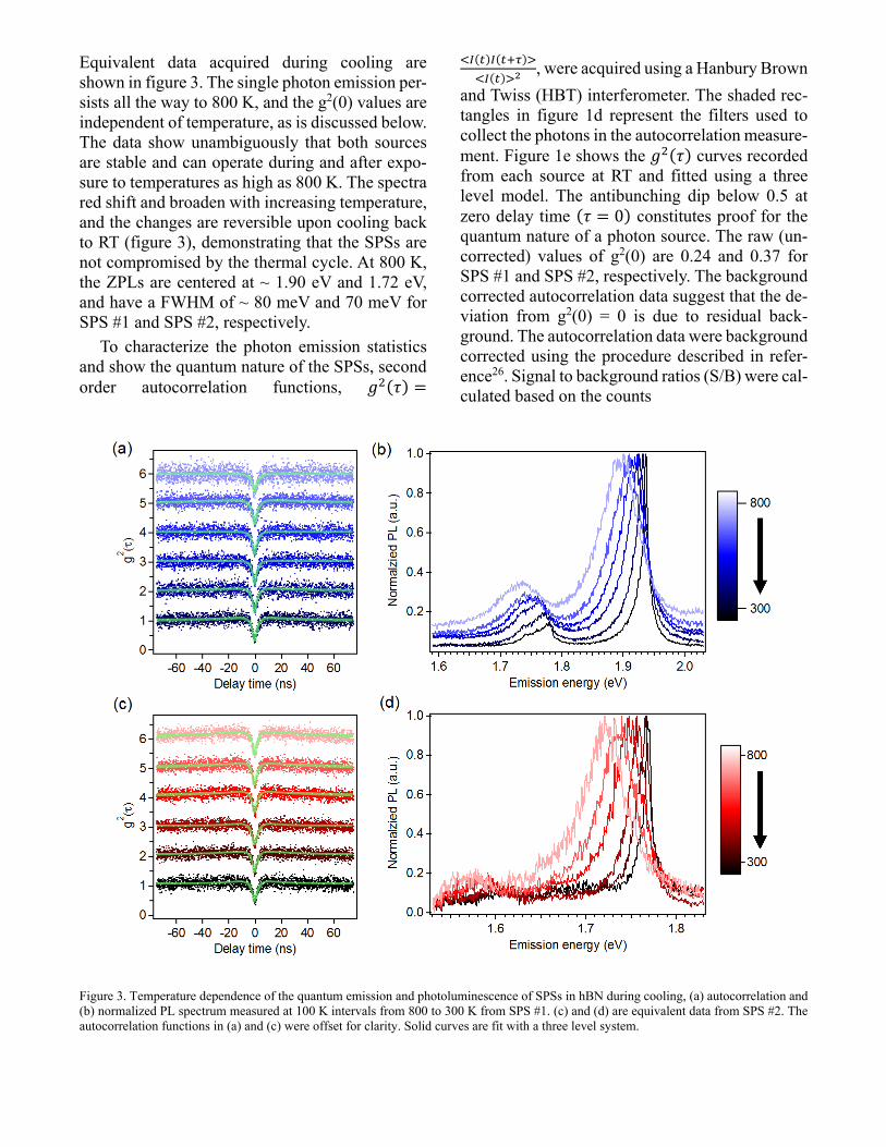
Equivalent data acquired during cooling are shown in figure 3. The single photon emission per-sists all the way to 800 K, and the g2(0) values are independent of temperature, as is discussed below. The data show unambiguously that both sources are stable and can operate during and after expo-sure to temperatures as high as 800 K. The spectra red shift and broaden with increasing temperature, and the changes are reversible upon cooling back to RT (figure 3), demonstrating that the SPSs are not compromised by the thermal cycle. At 800 K, the ZPLs are centered at ~ 1.90 eV and 1.72 eV, and have a FWHM of ~ 80 meV and 70 meV for SPS #1 and SPS #2, respectively.
To characterize the photon emission statistics and show the quantum nature of the SPSs, second order autocorrelation functions,
, were acquired using a Hanbury Brown and Twiss (HBT) interferometer. The shaded rec-tangles in figure 1d represent the filters used to collect the photons in the autocorrelation measure-ment. Figure 1e shows the curves recorded from each source at RT and fitted using a three level model. The antibunching dip below 0.5 at zero delay time 0 constitutes proof for the quantum nature of a photon source. The raw (un-corrected) values of g2(0) are 0.24 and 0.37 for SPS #1 and SPS #2, respectively. The background corrected autocorrelation data suggest that the de-viation from g2(0) = 0 is due to residual back-ground. The autocorrelation data were background corrected using the procedure described in refer-ence26. Signal to background ratios (S/B) were cal-culated based on the counts
Figure 3. Temperature dependence of the quantum emission and photoluminescence of SPSs in hBN during cooling, (a) autocorrelation and (b) normalized PL spectrum measured at 100 K intervals from 800 to 300 K from SPS #1. (c) and (d) are equivalent data from SPS #2. The autocorrelation functions in (a) and (c) were offset for clarity. Solid curves are fit with a three level system.
acquired when the excitation laser was focused on the source and when it was focused on the adjacent silicon substrate. The signal and background were measured at each temperature and the corrected coincidence (gc2) was obtained using the equation,
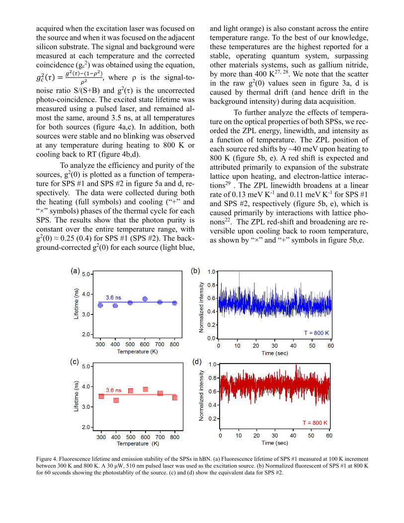
, where ρ is the signal-to-noise ratio S/(S+B) and g2() is the uncorrected photo-coincidence. The excited state lifetime was measured using a pulsed laser, and remained al-most the same, around 3.5 ns, at all temperatures for both sources (figure 4a,c). In addition, both sources were stable and no blinking was observed at any temperature during heating to 800 K or cooling back to RT (figure 4b,d).
To analyze the efficiency and purity of the sources, g2(0) is plotted as a function of tempera-ture for SPS #1 and SPS #2 in figure 5a and d, re-spectively. The data were collected during both the heating (full symbols) and cooling (“+” and “×” symbols) phases of the thermal cycle for each SPS. The results show that the photon purity is constant over the entire temperature range, with g2(0) ≈ 0.25 (0.4) for SPS #1 (SPS #2). The back-ground-corrected g2(0) for each source (light blue,
and light orange) is also constant across the entire temperature range. To the best of our knowledge, these temperatures are the highest reported for a stable, operating quantum system, surpassing other materials systems, such as gallium nitride, by more than 400 K27, 28. We note that the scatter in the raw g2(0) values seen in figure 3a, d is caused by thermal drift (and hence drift in the background intensity) during data acquisition.
To further analyze the effects of tempera-ture on the optical properties of both SPSs, we rec-orded the ZPL energy, linewidth, and intensity as a function of temperature. The ZPL position of each source red shifts by ~40 meV upon heating to 800 K (figure 5b, e). A red shift is expected and attributed primarily to expansion of the substrate lattice upon heating, and electron-lattice interac-tions29 . The ZPL linewidth broadens at a linear rate of 0.13 meV K-1 and 0.11 meV K-1 for SPS #1 and SPS #2, respectively (figure 5b, e), which is caused primarily by interactions with lattice pho-nons22. The ZPL red-shift and broadening are re-versible upon cooling back to room temperature, as shown by “×” and “+” symbols in figure 5b,e.
Figure 4. Fluorescence lifetime and emission stability of the SPSs in hBN. (a) Fluorescence lifetime of SPS #1 measured at 100 K increment between 300 K and 800 K. A 30 μW, 510 nm pulsed laser was used as the excitation source. (b) Normalized fluorescent of SPS #1 at 800 K for 60 seconds showing the photostablity of the source. (c) and (d) show the equivalent data for SPS #2.
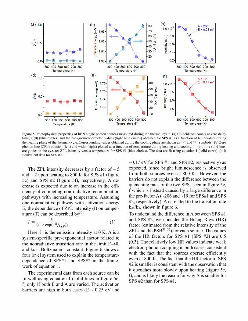
Figure 5. Photophysical properties of hBN single photon sources measured during the thermal cycle. (a) Coincidence counts at zero delay time, g2(0) (blue circles) and the background-corrected values (light blue circles) obtained for SPS #1 as a function of temperature during the heating phase of the thermal cycle. Corresponding values obtained during the cooling phase are shown as “×” and “+” symbols). (b) Zero phonon line (ZPL) position (left) and width (right) plotted as a function of temperature during heating and cooling. In (a-b) the solid lines are guides to the eye. (c) ZPL intensity versus temperature for SPS #1 (blue circles). The data are fit using equation 1 (solid curve). (d-f) Equivalent data for SPS #2.
The ZPL intensity decreases by a factor of ~ 5
and ~ 2 upon heating to 800 K for SPS #1 (figure 5c) and SPS #2 (figure 5f), respectively. A de-crease is expected due to an increase in the effi-ciency of competing non-radiative recombination pathways with increasing temperature. Assuming one nonradiative pathway with activation energy E, the dependence of ZPL intensity (I) on temper-ature (T) can be described by30:
(1)
Here, I0 is the emission intensity at 0 K, A is a system-specific pre-exponential factor related to the nonradiative transition rate in the limit E0, and kb is Boltzmann’s constant. Figure 6 shows a four level system used to explain the temperature-dependence of SPS#1 and SPS#2 in the frame-work of equation 1.
The experimental data from each source can be fit well using equation 1 (solid lines in figure 5c, f) only if both E and A are varied. The activation barriers are high in both cases (E ~ 0.25 eV and
~0.17 eV for SPS #1 and SPS #2, respectively) as expected, since bright luminescence is observed from both sources even at 800 K. However, the barriers do not explain the difference between the quenching rates of the two SPSs seen in figure 5c, f which is instead caused by a large difference in the pre-factor A (~206 and ~19 for SPS#1 and SPS #2, respectively). A is related to the transition rate k24/k42 shown in figure 6. To understand the difference in A between SPS #1 and SPS #2, we consider the Huang-Rhys (HR) factor (estimated from the relative intensity of the ZPL and the PSB31, 32) for each source. The values of the HR factors for SPS #1 (SPS #2) are 0.5 (0.3). The relatively low HR values indicate weak electron-phonon coupling in both cases, consistent with the fact that the sources operate efficiently even at 800 K. The fact that the HR factor of SPS #2 is smaller is consistent with the observation that it quenches more slowly upon heating (figure 5c, f), and is likely the reason for why A is smaller for SPS #2 than for SPS #1.

The difference is attributed to environmental fluc-tuations, which are believed to be responsible for the broad range of ZPL energies, widths and HR factors reported previously for quantum emitters in hBN19, 22, 23.
Figure 6. Simplified four level system used to explain the temper-ature-dependence of SPSs in hBN. The ground and excited states are labeled 1 and 2, 2.3 eV is the excitation energy used in our ex-periments, 1.94 eV (1.75 eV) is the ZPL energy of SPS #1 (SPS #2), E is the activation barrier in Equation 1, which equals 0.25 eV (and 0.17 eV) for SPS#1 (SPS#2), and k24 and k42 signify transition rates between states 2 and 4. The nonradiative recombination path-way proceeds through states 2, 4 and 3.
CONCLUSIONS
In conclusion, our work demonstrates robust SPSs that can operate at elevated temperatures of up to 800 K. The results open up exciting new pos-sibilities to integrate hBN SPSs with large scale, on-chip quantum photonic and optotelectronic de-vices that work under ambient conditions or ele-vated temperatures. Our results also provide vital information on stability, phonon coupling and photophysical properties of defects in layered ma-terials, stimulating further research in this area.
AUTHOR INFORMATION
Corresponding Author * Email: [email protected] ^Email: [email protected]
Author Contributions M.K., B. R. and T.T.T. contributed equally to this work. M.K. and B.R. carried out the experiments and M.K. and T.T.T. analyzed the data. The manuscript was prepared by contribution of all authors. I.A. and M.T. supervised the project.
ACKNOWLEDGMENT
Financial support from the Australian Research Council (via DP140102721, IH150100028, DE130100592), FEI Company, and the Asian Office of Aerospace Research and Development grant FA2386-15-1-4044 are gratefully acknowledged.
REFERENCES
1. Yuan Z, Kardynal BE, Stevenson RM, Shields AJ, Lobo CJ, Cooper K, et al. Electrically Driven Single-Photon Source. Science 2002, 295(5552): 102.
2. Mizuochi N, Makino T, Kato H, Takeuchi
D, Ogura M, Okushi H, et al. Electrically driven single-photon source at room temperature in diamond. Nature Photonics 2012, 6(5): 299-303.
3. Sun Y, Zhou K, Sun Q, Liu J, Feng M, Li
Z, et al. Room-temperature continuous-wave electrically injected InGaN-based laser directly grown on Si. Nature Photonics 2016, 10(9): 595-599.
4. Mamin HJ, Kim M, Sherwood MH,
Rettner CT, Ohno K, Awschalom DD, et al. Nanoscale Nuclear Magnetic Resonance with a Nitrogen-Vacancy Spin Sensor. Science 2013, 339(6119): 557-560.
5. Christle DJ, Falk AL, Andrich P, Klimov
PV, Hassan JU, Son NT, et al. Isolated electron spins in silicon carbide with millisecond coherence times. Nat Mater 2015, 14(2): 160-163.
6. Kuzmich A, Bowen WP, Boozer AD,
Boca A, Chou CW, Duan LM, et al. Generation of nonclassical photon pairs for scalable quantum communication with atomic ensembles. Nature 2003, 423(6941): 731-734.
7. O'Brien JL, Furusawa A, Vučković J. Photonic quantum technologies. Nature Photonics 2009, 3(12): 687-695.
8. Awschalom DD, Bassett LC, Dzurak AS,
Hu EL, Petta JR. Quantum Spintronics: Engineering and Manipulating Atom-Like Spins in Semiconductors. Science 2013, 339(6124): 1174.
9. Ladd TD, Jelezko F, Laflamme R,
Nakamura Y, Monroe C, O'Brien JL. Quantum computers. Nature 2010, 464(7285): 45-53.
10. Aharonovich I, Englund D, Toth M. Solid-
state single-photon emitters. Nat Photon 2016, 10(10): 631-641.
11. Fedorych O, Kruse C, Ruban A, Hommel
D, Bacher G, Kummell T. Room temperature single photon emission from an epitaxially grown quantum dot. Applied Physics Letters 2012, 100(6): 061114.
12. Kako S, Santori C, Hoshino K, Gotzinger
S, Yamamoto Y, Arakawa Y. A gallium nitride single-photon source operating at 200 K. Nat Mater 2006, 5(11): 887-892.
13. Castelletto S, Johnson BC, Ivády V,
Stavrias N, Umeda T, Gali A, et al. A silicon carbide room-temperature single-photon source. Nat Mater 2014, 13(2): 151-156.
14. Kurtsiefer C, Mayer S, Zarda P,
Weinfurter H. Stable Solid-State Source of Single Photons. Physical Review Letters 2000, 85(2): 290-293.
15. Aharonovich I, Castelletto S, Simpson
DA, Su CH, Greentree AD, Prawer S. Diamond-based single-photon emitters.
Reports on Progress in Physics 2011, 74(7): 076501.
16. Cassabois G, Valvin P, Gil B. Hexagonal
boron nitride is an indirect bandgap semiconductor. nature Photonics 2016, 10: 262-266.
17. Lin Y, Connell JW. Advances in 2D boron
nitride nanostructures: nanosheets, nanoribbons, nanomeshes, and hybrids with graphene. Nanoscale 2012, 4(22): 6908-6939.
18. Liu Z, Gong Y, Zhou W, Ma L, Yu J,
Idrobo JC, et al. Ultrathin high-temperature oxidation-resistant coatings of hexagonal boron nitride. Nat Commun 2013, 4: 2541.
19. Tran TT, Elbadawi C, Totonjian D, Lobo
CJ, Grosso G, Moon H, et al. Robust Multicolor Single Photon Emission from Point Defects in Hexagonal Boron Nitride. ACS Nano 2016, 10(8): 7331-7338.
20. Bourrellier R, Meuret S, Tararan A,
Stéphan O, Kociak M, Tizei LHG, et al. Bright UV Single Photon Emission at Point Defects in h-BN. Nano Letters 2016, 16(7): 4317-4321.
21. Tran TT, Zachreson C, Berhane AM, Bray
K, Sandstrom RG, Li LH, et al. Quantum Emission from Defects in Single-Crystalline Hexagonal Boron Nitride. Physical Review Applied 2016, 5(3): 034005.
22. Jungwirth NR, Calderon B, Ji Y, Spencer
MG, Flatte ME, Fuchs GD. Temperature Dependence of Wavelength Selectable Zero-Phonon Emission from Single Defects in Hexagonal Boron Nitride. Nano Lett 2016.
23. Chejanovsky N, Rezai M, Paolucci F, Kim
Y, Rendler T, Rouabeh W, et al. Topological attributes and photo-dynamics of visible spectrum quantum emitters in hexagonal boron nitride. arXiv:160803114 2016.
24. Martínez LJ, Pelini T, Waselowski V,
Maze JR, Gil B, Cassabois G, et al. Efficient single photon emission from a high-purity hexagonal boron nitride crystal. Physical Review B 2016, 94(12): 121405.
25. Choi S, Tran TT, Elbadawi C, Lobo CJ,
Wang X, Juodkazis S, et al. Engineering and localization of quantum emitters in large hexagonal boron nitride layers. arXiv:160804108 2016.
26. Beveratos A, Brouri R, Gacoin T, Poizat J-
P, Grangier P. Nonclassical radiation from diamond nanocrystals. Physical Review A 2001, 64(6).
27. Holmes MJ, Choi K, Kako S, Arita M,
Arakawa Y. Room-temperature triggered single photon emission from a III-nitride site-controlled nanowire quantum dot. Nano Lett 2014, 14(2): 982-986.
28. Holmes MJ, Kako S, Choi K, Arita M, Arakawa Y. Single Photons from a Hot Solid-State Emitter at 350 K. ACS Photonics 2016, 3(4): 543-546.
29. Varshni YP. Temperature dependence of
the energy gap in semiconductors. Physica 1967, 34(1): 149-154.
30. Lagomarsino S, Gorelli F, Santoro M,
Fabbri N, Hajeb A, Sciortino S, et al. Robust luminescence of the silicon-vacancy center in diamond at high temperatures. AIP Advances 2015, 5(12): 127117.
31. Huang K, Rhys A. Theory of Light
Absorption and Non-Radiative Transitions in F-Centres. Proceedings of the Royal Society of London Series A Mathematical and Physical Sciences 1950, 204(1078): 406.
32. Neu E, Steinmetz D, Riedrich-Moeller J,
Gsell S, Fischer M, Schreck M, et al. Single photon emission from silicon-vacancy centres in CVD-nano-diamonds on iridium New Journal of Physics 2011, 13: 025012.