RF fingerprinting physical objects for anticounterfeiting applications
11
504 IEEE TRANSACTIONS ON MICROWAVE THEORY AND TECHNIQUES, VOL. 59, NO. 2, FEBRUARY 2011 RF Fingerprinting Physical Objects for Anticounterfeiting Applications Vasileios Lakafosis, Student Member, IEEE, Anya Traille, Hoseon Lee, Edward Gebara, Member, IEEE, Manos M. Tentzeris, Fellow, IEEE, Gerald R. DeJean, Member, IEEE, and Darko Kirovski, Member, IEEE Abstract—Rendering typical RF identification (RFID) tags physically unique and hard to near-exactly replicate by com- plementing them with unique RF certificates of authenticity (RF-CoAs) can prove a valuable tool against counterfeiting. This paper introduces a new robust RFID system with enhanced hard- ware-enabled authentication and anticounterfeiting capabilities that relies on the near-field RF effects between a 5 5 antenna array and the uniquely modified substrate of the RF-CoAs. A microcontroller-enabled, low-power, and low-cost reader is used to accurately extract the near-field response (“RF fingerprint”) of the certificates meant to complement typical RFID tags in the 5–6-GHz frequency range. The RF characterization of all the reader’s components, with an emphasis on the accuracy provided, has been performed. The state diagram of the fast and accurate reader operation is outlined. Rigorous performance and security test results are presented and verify the unique features of this technology. Index Terms—Anticounterfeiting, multiantenna systems, near- field, RF certificate of authenticity (RF-CoA), RF fingerprint, RF identification (RFID), wireless. I. INTRODUCTION W ITH THE World Customs Organization and Interna- tional Chamber of Commerce, according to Interpol, estimating that roughly 8% of world trade every year is in coun- terfeit goods [1], the Business Software Alliance estimating that 35%–45% of software sales worldwide are counterfeit [2], and Glaxo-Smith-Kline, in a study with the U.S. Food and Drug Ad- ministration, estimating that counterfeit drugs account for 10% of the global pharmaceuticals market [3], there is no doubt that counterfeiting accounts for a huge economic impact on indus- tries such as software and hardware, pharmaceutical, and, of course, the entertainment and fashion industry. With the ease of marketing products on-line, it seems that selling counterfeit objects has never been easier. Manuscript received September 07, 2010; revised October 13, 2010 and November 01, 2010; accepted November 08, 2010. Date of publication December 30, 2010; date of current version February 16, 2011. This work was supported in part by the IFC/SRC. This paper is an expanded paper from the IEEE MTT-S International Microwave Symposium, Anaheim, CA, May 23–28, 2010. V. Lakafosis, A. Traille, H. Lee, E. Gebara, and M. M. Tentzeris are with the School of Electrical and Computer Engineering, Georgia Institute of Tech- nology, Atlanta, GA 30308 USA (e-mail: [email protected]; atraille@ece. gatech.edu; [email protected]; [email protected]; [email protected]. edu). G. R. DeJean and D. Kirovski are with Microsoft Research, Redmond, WA 98052 USA (e-mail: [email protected]; [email protected]). Color versions of one or more of the figures in this paper are available online at http://ieeexplore.ieee.org. Digital Object Identifier 10.1109/TMTT.2010.2095030 In contrast with piracy, where the buyer is confident that the purchased object is not genuine due to a very low price, the counterfeiter fools the buyer into believing that the merchandise is authentic and collects substantial revenue with profit margins typically higher than that of the original manufacturer. In the battle against piracy and counterfeiting, traditional RF identi- fications (RFIDs) with encoded digital information cannot be relied upon since they can easily be replicated. This paper presents the full implementation of a novel RF anticounterfeiting system that aims to address this problem in a completely hardware-based (“RF-fingerprinting”) way. This is the first reported approach that aims to bridge the RFID tech- nologies with the anticounterfeiting world utilizing modified material scattering characteristics. The fundamental idea is to complement an RFID with an inexpensive physical object that behaves as an RF certificate of authenticity (RF-CoA) in the electromagnetic (EM) field so that this “super-tag” is not only digitally, but also physically unique and hard to near-exactly replicate. The RF-CoA can be created as a random constellation of small, randomly 3-D-shaped conductive and/or dielectric ob- jects that exhibits a distinct behavior in its near-field when ex- posed to RF waves coming from a specific point over a partic- ular RF spectrum. This enables, on one hand, the extraction of the data about the product in the far-field and, on the other hand, the verification of its authenticity within its near-field with low probability of a false alarm. Fundamental to the following discussion is the definition of the “RF Fingerprint.” An “RF fingerprint” of an RF-CoA is a set of parameters observed over a specific frequency band and collected for (a subset of or) all possible antenna couplings of a reader’s array. The main aim of the reader design, pre- sented below, is to maximize the entropy, i.e., randomness, of the “RF fingerprint,” given the accuracy of the analog and dig- ital circuitry used, as well as the noise due to external factors. A graphical representation of this fingerprint, as extracted from the reader for all its 72 different antenna element permutations using a signal processing method described in detail in Section VI, is shown in Fig. 1. II. RELATED WORK CoAs in the RF domain have been proposed in the past 1 2 [4], [5]. The common characteristic of all proposed solutions, to the best of our knowledge, is that they aim to detect the 1 Inkode Inc., Vienna, VA, 2007. [Online.] Available: http://www.inkode.com 2 RF SAW Inc., Richardson, TX, 2007. [Online.] Available: http://www.rfsaw. com/tech.html 0018-9480/$26.00 © 2010 IEEE
-
Upload
independent -
Category
Documents
-
view
2 -
download
0
Transcript of RF fingerprinting physical objects for anticounterfeiting applications

504 IEEE TRANSACTIONS ON MICROWAVE THEORY AND TECHNIQUES, VOL. 59, NO. 2, FEBRUARY 2011
RF Fingerprinting Physical Objects forAnticounterfeiting Applications
Vasileios Lakafosis, Student Member, IEEE, Anya Traille, Hoseon Lee, Edward Gebara, Member, IEEE,Manos M. Tentzeris, Fellow, IEEE, Gerald R. DeJean, Member, IEEE, and Darko Kirovski, Member, IEEE
Abstract—Rendering typical RF identification (RFID) tagsphysically unique and hard to near-exactly replicate by com-plementing them with unique RF certificates of authenticity(RF-CoAs) can prove a valuable tool against counterfeiting. Thispaper introduces a new robust RFID system with enhanced hard-ware-enabled authentication and anticounterfeiting capabilitiesthat relies on the near-field RF effects between a 5 5 antennaarray and the uniquely modified substrate of the RF-CoAs. Amicrocontroller-enabled, low-power, and low-cost reader is usedto accurately extract the near-field response (“RF fingerprint”)of the certificates meant to complement typical RFID tags in the5–6-GHz frequency range. The RF characterization of all thereader’s components, with an emphasis on the accuracy provided,has been performed. The state diagram of the fast and accuratereader operation is outlined. Rigorous performance and securitytest results are presented and verify the unique features of thistechnology.
Index Terms—Anticounterfeiting, multiantenna systems, near-field, RF certificate of authenticity (RF-CoA), RF fingerprint, RFidentification (RFID), wireless.
I. INTRODUCTION
W ITH THE World Customs Organization and Interna-tional Chamber of Commerce, according to Interpol,
estimating that roughly 8% of world trade every year is in coun-terfeit goods [1], the Business Software Alliance estimating that35%–45% of software sales worldwide are counterfeit [2], andGlaxo-Smith-Kline, in a study with the U.S. Food and Drug Ad-ministration, estimating that counterfeit drugs account for 10%of the global pharmaceuticals market [3], there is no doubt thatcounterfeiting accounts for a huge economic impact on indus-tries such as software and hardware, pharmaceutical, and, ofcourse, the entertainment and fashion industry. With the easeof marketing products on-line, it seems that selling counterfeitobjects has never been easier.
Manuscript received September 07, 2010; revised October 13, 2010 andNovember 01, 2010; accepted November 08, 2010. Date of publicationDecember 30, 2010; date of current version February 16, 2011. This workwas supported in part by the IFC/SRC. This paper is an expanded paper fromthe IEEE MTT-S International Microwave Symposium, Anaheim, CA, May23–28, 2010.
V. Lakafosis, A. Traille, H. Lee, E. Gebara, and M. M. Tentzeris are withthe School of Electrical and Computer Engineering, Georgia Institute of Tech-nology, Atlanta, GA 30308 USA (e-mail: [email protected]; [email protected]; [email protected]; [email protected]; [email protected]).
G. R. DeJean and D. Kirovski are with Microsoft Research, Redmond, WA98052 USA (e-mail: [email protected]; [email protected]).
Color versions of one or more of the figures in this paper are available onlineat http://ieeexplore.ieee.org.
Digital Object Identifier 10.1109/TMTT.2010.2095030
In contrast with piracy, where the buyer is confident that thepurchased object is not genuine due to a very low price, thecounterfeiter fools the buyer into believing that the merchandiseis authentic and collects substantial revenue with profit marginstypically higher than that of the original manufacturer. In thebattle against piracy and counterfeiting, traditional RF identi-fications (RFIDs) with encoded digital information cannot berelied upon since they can easily be replicated.
This paper presents the full implementation of a novel RFanticounterfeiting system that aims to address this problem in acompletely hardware-based (“RF-fingerprinting”) way. This isthe first reported approach that aims to bridge the RFID tech-nologies with the anticounterfeiting world utilizing modifiedmaterial scattering characteristics. The fundamental idea is tocomplement an RFID with an inexpensive physical object thatbehaves as an RF certificate of authenticity (RF-CoA) in theelectromagnetic (EM) field so that this “super-tag” is not onlydigitally, but also physically unique and hard to near-exactlyreplicate.
The RF-CoA can be created as a random constellation ofsmall, randomly 3-D-shaped conductive and/or dielectric ob-jects that exhibits a distinct behavior in its near-field when ex-posed to RF waves coming from a specific point over a partic-ular RF spectrum. This enables, on one hand, the extraction ofthe data about the product in the far-field and, on the other hand,the verification of its authenticity within its near-field with lowprobability of a false alarm.
Fundamental to the following discussion is the definition ofthe “RF Fingerprint.” An “RF fingerprint” of an RF-CoA is aset of parameters observed over a specific frequency bandand collected for (a subset of or) all possible antenna couplingsof a reader’s array. The main aim of the reader design, pre-sented below, is to maximize the entropy, i.e., randomness, ofthe “RF fingerprint,” given the accuracy of the analog and dig-ital circuitry used, as well as the noise due to external factors. Agraphical representation of this fingerprint, as extracted from thereader for all its 72 different antenna element permutations usinga signal processing method described in detail in Section VI, isshown in Fig. 1.
II. RELATED WORK
CoAs in the RF domain have been proposed in the past1 2
[4], [5]. The common characteristic of all proposed solutions,to the best of our knowledge, is that they aim to detect the
1Inkode Inc., Vienna, VA, 2007. [Online.] Available: http://www.inkode.com2RF SAW Inc., Richardson, TX, 2007. [Online.] Available: http://www.rfsaw.
com/tech.html
0018-9480/$26.00 © 2010 IEEE

LAKAFOSIS et al.: RF FINGERPRINTING PHYSICAL OBJECTS FOR ANTICOUNTERFEITING APPLICATIONS 505
Fig. 1. Graphical representation of an “RF fingerprint” as extracted by our fab-ricated reader for all its 72 different antenna element permutations.
CoA’s random structure in the far-field over the “expensive”60-GHz frequency range. Under the same far-field category, butin the 5–7-GHz frequency band, also falls a printable chiplessRFID tag [6] presented for secure banknote applications, theanticounterfeiting robustness of which relies only on a bit se-quence formed by a multiresonating circuit.
Our proposed system, the operation of which relies on thenear-field observation of the CoA’s EM (scattering) effects,possesses some important qualitative features not exhibitedby other types of CoAs. First of all, the near-field observa-tion enables relatively high variance of the EM field, causingbetter discriminating characteristics compared to the far-fieldresponses that typically represent certain average characteris-tics of random discrete scatterers [7]. Characteristics of thisnear-field region, which is located less than one wavelength(more precisely, , where is the largest dimensionof the source of the radiation) from the source, are that therelationship between the electric field component and themagnetic field component becomes often too complex topredict with either field component ( or ) possibly dom-inating at any particular point and that all four polarizationtypes, namely, horizontal, vertical, circular, or elliptical, canbe present, as opposed to the far field. Still, since the readoutof the CoA does not require a physical contact, RF-CoAs maybe built with superior “wear and tear” properties. Second, it ishard to eavesdrop or maliciously jam near-field communicationcompared to the far-field one that is prone to both potentiallydevastating attacks. As an additional advantage of the veryshort-range observation and discrimination feature, the readercan operate with low power and use low-efficiency antennadesigns.
III. RF-CoA TECHNOLOGY
A. Fabrication Process
This process takes place in the controlled environment of anRF-CoA factory. Here, after an RF-CoA instance is created,the issuer digitally signs the instance’s RF response using tradi-tional cryptography.
In particular, first the unique “RF fingerprint” of the newlyfabricated RF-CoA instance is digitized with the use of a readerand compressed into a fixed-length bit string. This informationis afterward concatenated to the information associated with the
tag, such as product ID, color, and expiration date, and the re-sulting combined bit string is encrypted using a cryptographi-cally strong algorithm such as SHA256 [8].
Adopting a public-key cryptosystem (PKCS) such as Rivest,Shamir, and Adleman (RSA) [9], this hash is signed using theissuer’s private key to form, together with the plain initial bitstring of the fingerprint, a message that is directly encoded ontothe RFID chip. The use of asymmetric key algorithms that in-volve the use of a public key known to everyone and a secret pri-vate key is the distinguishing characteristic of public key cryp-tography. The keys are related mathematically, but it is virtuallyimpossible to deduce the private key from the public key. Thus,in our application only the issuer can digitally sign the RF-CoAwith the secret private key.
B. Verification Process
The digitally encoded message, described above, is the oneused to validate whether a product is authentic or not; a processthat typically takes place in a store or a warehouse.
The verifier first reads the aforementioned message andverifies the integrity of the plain bit string of the fingerprintwith respect to its encrypted and signed version using thecorresponding issuer’s public key. In case the integrity test issuccessful, which means that no one else, except the possessorof the matching private key, has encrypted the message, theoriginal “RF fingerprint” and associated product data are ex-tracted. This extracted fingerprint is afterward compared witha new reading of the tag’s CoA that the verifier takes withhis own reader. Only if the level of similarity between thesetwo fingerprints, read and extracted, exceeds a predefined andstatistically validated threshold, the verifier declares the CoAinstance to be authentic.
C. Potential Attacks
In order for an adversary to counterfeit protected objects, heneeds to do the following:
1) compute the private key of the issuer so that he can storehis one fixed-length bit string f; a task which can bemade arbitrarily difficult by adjusting the key length ofthe used public-key crypto-system, or
2) misappropriate signed CoA instances; a responsibility ofthe CoA object issuer, or
3) devise a manufacturing process that can exactly ornearly exactly replicate an already signed CoA in-stance; a task that is not infeasible, but requires certainexpense by the malicious party. In particular, ourRF-CoA designs require by the counterfeiter not onlyphysical access to the original CoA, but also the abilityto accurately scan and reconstruct arbitrary 3-D struc-tures and embed them in a soft or hard encapsulatingsealant; a high-cost process.
From the last attack’s perspective, it is obvious that the CoAscan be used to protect objects, the value of which does not ex-ceed the cost of forging a single CoA instance including the ac-cumulated development cost of a successful adversarial manu-facturing process.

506 IEEE TRANSACTIONS ON MICROWAVE THEORY AND TECHNIQUES, VOL. 59, NO. 2, FEBRUARY 2011
Fig. 2. CoAs of different copper weight, namely, 2, 3, and 4 g per mold.
IV. RF-CoA TAG
The proposed RF-CoA tag is the first low-cost physical ob-ject that enables anticounterfeiting based completely on its hard-ware implementation and the resulting RF effects. The physicalRF-CoA instance consists of an extremely difficult to replicate,random arrangement of scatterers that produces a unique and re-peatable response in the near field. Since the RF-CoA instanceis completely passive, it is imperative that every different scat-ters’ configuration should provide a unique RF signature withinthe frequency range of the reader’s illumination based only onthe spatial arrangement.
As is also the case with the reader, the design of these an-ticounterfeiting tags has to be optimized so that maximum en-tropy of the scattering results is achieved, and in the same time,the results extracted by the same instance are repeatable withvery high reliability. This optimization is challenging, as it isnecessary to perform a detailed systematic analysis of variousnear-field phenomena by investigating distinct geometries forthe RF-CoA design. The first and most important factor to con-sider is the individual scatterers’ resonance and interference incompact “credit-card” size dimensions. Other factors to con-sider include the dimensions of the spaces between conductorsas a fraction of reader’s wavelength and how the RF-CoA’s scat-terers’ nonperiodicity affects the response for various densities.These parameters are expected to be critical in the determinationof the system’s discrimination capability that will effectively de-cide how easy RF-CoAs can be counterfeited in a given centralfrequency, bandwidth, and RF-CoA’s dimensions.
The tags can be divided into two main categories, namely,the copper-based ones and the inkjet-printed ones. Examples ofthe first category are shown in Fig. 2 and are used throughoutSection VII for all the performance tests. These have been fabri-cated by an injection molding company3; essentially the processinvolves the encapsulation of copper wire of variable gauge intoplastic mold. Randomness in this process has been achievedby introducing techniques that are absolutely nondeterministic,such as blending with different speeds and for different amountof time and using air fans.
As for the second category of physical RF-CoA objects, werelied upon inkjet printing technique as a means of a very fast,low-cost, and in-house process; a direct-write technique bywhich the design pattern is transferred directly to the substratein means of multiple inkjet layers, without any requirement ofmasks. The final 3-D structure was created by tightly stacking
3Aero-plastics Inc., Renton, WA, 2009. [Online.] Available: http://www.aero-plastics.tmcsweb.com/
Fig. 3. (a) “RF plane” and “control plane” of the RF-CoA reader. (b) Overallstacked two-layer RF-CoA system.
multiple 2-D CoAs one on top of each other to give the projec-tion, shown in Section VIII, and are used for the 3-D attacks testdescribed in Section VIII.
V. RF-CoA READER
The extraction of the unique RF fingerprint of an RF-CoAobject is done as follows. RF power is radiated from a partic-ular element of the antenna array, scattered and reflected bythe conductive material of the RF-CoA instance placed about1 mm away from the array and received by another antenna ele-ment. During the readout, it is ensured that the placement of theRF-CoA instance is fixed and geometrically unique, using shortplastic poles, shown in Fig. 3(b), the relative position of whichon the array’s plane is nonsymmetrical.
The overall design, shown in Fig. 4, consists of four metallicand three substrate layers of variable thickness and the totalthickness does not exceed 1.6 mm. The elements of the antennaarray are placed on the top and second metal layers at distancesof approximately 3 mm between each other. The ground plane isplaced on the third metal layer, the RF part on the bottom layerand the digital lines on the top layer. The copper’s conductivityis 5.88 10 S/m 1.493 10 S/in . The substrate for the de-sign is FR-408 with relative dielectric constant inour frequency band of interest (5–6 GHz), relative permeability
, and loss tangent .

LAKAFOSIS et al.: RF FINGERPRINTING PHYSICAL OBJECTS FOR ANTICOUNTERFEITING APPLICATIONS 507
Fig. 4. RF-COA reader circuit schematic.
Fig. 5. ��� curve of an individual antenna element. Its 3-D design is shown inthe lower right corner.
A. Antenna Elements and Coupling
The antenna elements are individual microstrip patch an-tennas. Since it was desired to pack as many antennas aspossible in a 1 1 in area, emphasis was stressed on makinguse of a folding minimization technique; the antenna’s technicalcharacteristics and design strategy are detailed in [10]. Giventhat the half-wavelength in this range of frequencies is around2.75 cm and given the properties of the folding minimizationtechnique, we were finally able to fit 25 elements.
The antenna’s 3-D element design is shown in the insert figureof Fig. 5. A single such element has a return loss of 16.3 dB4 ata resonant frequency of 5.149 GHz (when a single element ismeasured by itself and not in the presence of neighboring ele-ments), as shown in Fig. 5. The aforementioned miniaturizationtechnique, however, does not come without cost and the majornegative effect is the limited 10-dB bandwidth of this antenna el-ement, which does not exceed 5 MHz. Despite that, the strengthof the electric field extracted by these elements even 0.5 GHzaway from the resonant frequency can be very high ( 10 dB),as shown in performance tests of Section VII.
Out of all the 25 elements of the 5 5 antenna matrix, nine ofthem are operating as transmit-only and eight of them as receive-
4Using the Rohde & Schwarz ZVA 8 vector network analyzer (VNA).
Fig. 6. Diagram of the functionality of the reader’s 5 � 5 antenna arrayelements.
only, eliminating the need for single-pole double-throw (SPDT)switches for dual operation of the elements and reducing thenumber of the required digital input/output control lines. Thispattern is shown in Fig. 6.
The reason that each of the transmit- and receive-only ele-ments have been split into sets of fours, placed as farthest aspossible in the four corners of the array, and that the rest of theeight elements on the cross of the structure, with the exceptionof the central one, have been rendered useless (unconnected) isthat we wanted to minimize the coupling due to proximity and,thus, attribute most of the coupling measured to the presenceof the metallic material of the CoA. To quantify this, thecurves of all possible different antenna element spacings of astandalone 3 3 antenna array in the absence of any CoA isshown in Fig. 7 (bottom). This array has been manufactured inthe exact same way as the finally used 5 5 array so that sub-miniature A (SMA) RF connectors are available and more intu-itive conclusions can be drawn by fewer elements. These six dif-ferent curves, captured over the 4.6–6.4-GHz band for 3-MHzstep sizes, are labeled with a “ – ” format corresponding to the“ ” numbered element, as shown in Fig. 7 (top), transmittingand the “ ” numbered element receiving. As expected, all curveshave their maximum at around the resonant frequency of the an-tenna elements and the shorter the relative distance the higherthis maximum is .It should be noted that the worst case scenario for the actual5 5 board and given the functionality assigned to the activeelements, described above and shown in Fig. 6, corresponds tothe cases of 1–2 and 2–3 (C3-B4 and C3-D2), for which themagnitude of the maximum points does not exceed 20 dB. Inother words, the maximum coupling between any pair of ele-ments of the 5 5 array in the absence of a CoA never exceeds20 dB.
B. Single-Pole Four-Throw (SP4T) Switches
A particular antenna transmit and receive coupling, out of theboard’s 72 possible permutations, is chosen by digitally control-ling eight identical HMC345LP3 [11] SP4T switches, arrangedin two hierarchical levels, as shown in the block diagram ofFig. 8. Based on this arrangement, there are always two switchespreceding the transmit-only antenna element and two switchesfollowing the receive-only element. The location and order ofthe switches has been optimized so that the coupling betweenthe RF lines is minimal. In particular, all connections are 50

508 IEEE TRANSACTIONS ON MICROWAVE THEORY AND TECHNIQUES, VOL. 59, NO. 2, FEBRUARY 2011
Fig. 7. (top) Bottom view of a 3� 3 antenna array fabricated in the exact sameway as the reader’s 5 � 5 array. (bottom) � curves of all possible differentantenna element spacings of a subset 3� 3 array in the absence of any CoA.
Fig. 8. SP4T switches arranged in two hierarchical levels.
and it has been ensured that the length of the lines connecting theappropriate switches for any antenna permutation is constant.
The average insertion loss introduced by a single SP4T switchacross the 4.5–6.5-GHz band has been measured 1.074 dB.5 The
and parameters of the two-port system between thetransmit and receive power amplifiers (PAs) have been shownin [12].
The losses of the reader’s components are expected to varyfrom lot of circuit components to lot and, as a result, from readerto reader. In order to achieve consistency and elimination offalse negatives among different readers, i.e., for calibrationpurposes, all coupling channels for all possible antennapermutations over the whole supported frequency band aremeasured for each RF-CoA reader in the absence of any CoAand stored into the Microcontroller Unit’s (MCU) nonvolatilememory. Right after the CoA’s fabrication, these curves
5Using the Rohde & Schwarz ZVA 8 VNA.
are subtracted from the corresponding curves of the CoA’sRF fingerprint and the difference is what becomes embeddedin the RFID chipset. The same “subtraction,” of course, takesplace also at the verifier’s premises.
VI. MCU-ENABLED READER OPERATION
The functionality of the RF-CoA reader is summarized in thefollowing four main tasks:
• generates the appropriate RF power and controls the fre-quency output of the voltage-controlled oscillator (VCO);
• dictates the path that the RF signal follows through the two-layer SP4T switch hierarchy and the coupling, eventuallybetween the and antenna element;
• measures the power captured by the power detector (PD)by monitoring its output voltage;
• uploads the set of measured data that comprise theRF-CoA’s fingerprint to a computer.
The most important advancement in regards with the first ver-sion of the RF-CoA board, presented in [12], has been the ad-dition of a 16-bit RISC architecture ultra-low-power MCU thatprovides not only a very fast means of capturing the RF finger-print, but also the accuracy required toward our effort to max-imize the fingerprint’s entropy. As a result, the overall readerdesign consists of a double-stacked-layer solution; the “controlplane” and the “super high frequency (SHF) RF plane.” As im-plied by their names, the first layer houses the MCU and the dataacquisition interface and the other includes the CoA readingslot, the antenna matrix, as well as all required digital and analogcircuitry. The upper layer of this new prototype RF-CoA reader,represented with pink lines (in online version) in Fig. 4, is the“control plane” and the lower one, represented with green lines(in online version) is the “SHF RF plane.”
Regarding the “SHF RF plane,” it should be noted that itsdesign is an improved version of our preliminary design [12].First, this new board is smaller in its width, occupying 13% lessspace (4.301 6.775 in). Second, this design does not rely ona single VCO, but two of them, namely, the HMC430LP4 [13]and HMC431LP4 [14], which both together optimally cover the5.0–6.1-GHz frequency band.
At the heart of the “control plane” is the TI MSP-EXP430F5438 MCU [15] that features an up to 18-MHzsystem clock, high-frequency crystals up to 32 MHz and mul-tiple high-resolution analog-to-digital converters (ADCs). TheMCU is accompanied by push buttons and a USB interface fordata transfer. The state diagram of the MCU, which reflects thesequence of all the steps mentioned in the beginning of thissection, is shown in Fig. 9.
For its powering, the “control plane” does not rely on bat-teries (although a 2 AA battery option is available), but on thecurrent supplied by the USB cable, which is used anyway forthe RF-CoA fingerprint acquisition by a desktop or a laptopcomputer. When the board is initially connected to a computerthrough the USB cable, it finds itself in the low-power mode 4(LPM4) sleep mode. This is a deep sleep mode of 1.69- A cur-rent consumption at 3.0 V in which the CPU and all clocks aredisabled, the crystal oscillator is stopped, but the supply super-visor is operational and full RAM retention and fast wake-upare provided.

LAKAFOSIS et al.: RF FINGERPRINTING PHYSICAL OBJECTS FOR ANTICOUNTERFEITING APPLICATIONS 509
Fig. 9. State diagram of the RF-CoA reader’s operation.
In short time intervals, the 32-kHz auxiliary clock is enabledand used to check if a button is pressed. Given that a humanwould be pressing the button for at least half a second, the timeduration of this button monitoring lasts for only a few millisec-onds, leading eventually to a very low duty cycle monitoring.As soon as a press on the button is detected, the MCU exits thedeep sleep mode and the “control plane” transits to the antennapermutation selection state. Here, a particular antenna elementpair is selected by appropriately configuring the two digital logiccontrol pins (0 for logical 0 and 3.2 for logical 1) ofthe SP4T switches, shown in Fig. 9. In particular, a 16-bit se-quence is generated by the digital output pins of the MCU andthis selection remains active until a new bit sequence is gener-ated. The next time the “control plane” returns to the antennapermutation selection state, a check is performed as to whetherthe maximum number of antenna permutations (NUM_ELEM),namely, 72, has already been selected; in which case the MCUreverts to the sleep mode.
If all possible antenna element permutations have not beenenabled, the next step is to generate a sinusoidal power signalat a particular frequency, nearly monochromatic, by controllingthe HMC431LP4 [14] VCO. The peak power of this signal, afterit is amplified by 11.25 dB by the RF3378 [16] PA, is measuredto be 4.03 dBm.6 The RF-CoA fingerprint is captured overthe frequency band of 5.1–5.9-GHz at steps of 12.3 MHz. Theselection of these steps is achieved by altering the VCO’s tunevoltage. Since the MCU provides no DACs, the latter’s function-ality is emulated by a high-frequency pulsewidth modulation(PWM) signal. The output voltage is configured based on a vari-able duty cycle that is derived from the ratio between the PWM’semulated voltage and the USB rail of 3.2 V. The next time the“control plane” returns to the control VCO state, a check is per-formed as to whether the maximum number of frequency steps(maxFreq) has already been reached; in which case the MCUreturns to the antenna permutation selection state.
6Tektronix RSA 3408A real-time spectrum analyzer (RSA).
Fig. 10. Standard deviation of eight antenna coupling for the repeatability test.
With the antenna element radiating power toward the CoAthat is placed just 1 mm away from the antenna matrix, the nextstep is to amplify the captured reflected and refracted signal andfeed it to the LT5581 root mean square (rms) [17] PD. For cali-bration purposes, the latter’s voltage output has been accuratelymapped to the input power generated by a signal generator7 be-fore the PA ranging from 55 up to 5 dBm. For this task, ofcourse, the highest (12-bit precision) mode supported by theADC of the MCU is chosen.
Regarding the effective bit length of entropy (EBLE)achieved with the results presented in the next two sections,this number cannot be cited as simply permutations
frequencies bit of resolution bitssince interdependencies of all responses need to be taken intoaccount. However, our achieved EBLE is substantially higherthan what common cryptographic standards demand.
Based on extensive measurements carried out under a con-trolled environment of predetermined signal power amplitude,
7HP 83622B Swept Signal Generator.

510 IEEE TRANSACTIONS ON MICROWAVE THEORY AND TECHNIQUES, VOL. 59, NO. 2, FEBRUARY 2011
Fig. 11. “RF fingerprints” of ten different CoAs for four different antenna cou-plings for the “false positives” test.
we have found that a single analog-to-digital conversion isnot enough. In particular, although the voltage reference used(3.2 V) for the ADC and supplied by the USB input has beenmeasured to remain steady over time, we have recorded ADconversions to be as far as 20% off from the same actual inputsignal for more than 100 measurements. The two major sourcesof inaccuracy in ADC testing of mixed-signal circuits havebeen identified to be the approximations of IEEE Standard forDigitizing Waveform Recorders and IEEE Standard for Termi-nology and Test Methods for ADCs [18] and the fact that thedc offset and the amplitude of the input analog signal evaluated
Fig. 12. Standard deviation of ten different � curves shown in Fig. 11 forfour antenna couplings.
on the base of the digital output differ from their true values[19]. However, this deviation easily drops to less than 8% byperforming 20 consecutive conversions, storing them in thesuccessive approximation register (SAR) and afterward simplyaveraging them. The latency incurred as a result of the addi-tional 19 conversions is totally negligible given that each 12-bitresolution conversion requires only 13 MCU clock cycles, thetotal time duration of which is less than 0.8 s. The NUM_AVGvariable shown in the state diagram of Fig. 9 corresponds tothe maximum number, i.e., 20, of consecutive analog-to-digitalconversions before the averaging is performed.
Each entry consisting of antenna permutation, frequency,and received power in decibels is uploaded to the computer at57.6 kb/s with the use of the USCI module of the MCU thatsupports the UART protocol used to communicate with the TITUSB chip. An LED that remains on until all the aforemen-tioned steps for the RF fingerprint extraction are completed isindicative of the activity of the “control plane” before it returnsback to its sleep mode state. For this currently running softwareversion, where significantly conservative long guard times arekept between consecutive operations that account for a multipleof the real running time, and which will gradually be removedfrom the next software versions, the overall time required toextract all 72 RF fingerprints is around 22 s.
VII. PERFORMANCE TESTS
A number of different types of tests have been conducted inorder to assess the performance of our proposed RF authenticitycertification technology. For all tests presented in this section,physical objects that are conceptually very close to the final en-visioned product have been used as RF-CoAs. These objects aredescribed in Section IV and examples of such three certificatesare shown in Fig. 2.
As explained previously, the RF-CoA instances were at-tached to the reader through the plastic poles, shown inFig. 3(b), against the antenna matrix of the manufacturedRF-CoA reader at a distance of 1 mm. For this 1-mm spacing, asturdy dielectric foam material with characteristics close to thatof air was used. The certificates’ dimensions were 0.75 in0.75 in and as such could not occupy the whole 1 in 1 in areaof the antenna matrix. However, their position has been rotatedaround the array’s central axis so that not all areas around the
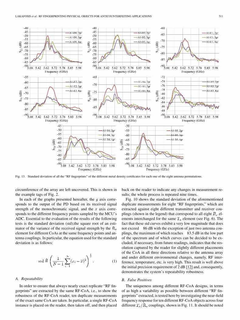
LAKAFOSIS et al.: RF FINGERPRINTING PHYSICAL OBJECTS FOR ANTICOUNTERFEITING APPLICATIONS 511
Fig. 13. Standard deviation of all the “RF fingerprints” of the different metal density certificates for each one of the eight antenna permutations.
circumference of the array are left uncovered. This is shown inthe example tags of Fig. 2.
In each of the graphs presented hereafter, the axis corre-sponds to the output of the PD based on its received signalstrength of the monochromatic signal, and the axis corre-sponds to the different frequency points sampled by the MCU’sADC. Essential to the evaluation of the results of the followingtests is the standard deviation (std);the square root of an esti-mator of the variance of the received signal strength by theelement for different CoAs at the same frequency points and an-tenna couplings. In particular, the equation used for the standarddeviation is as follows:
(1)
A. Repeatability
In order to ensure that always nearly exact replicate “RF fin-gerprints” are extracted by the same RF-CoA, i.e., to show therobustness of the RF-CoA reader, ten duplicate measurementsof the exact same CoA are taken. In particular, a single RF-CoAinstance is placed on the reader, then taken off, and then placed
back on the reader to indicate any changes in measurement re-sults; the whole process is repeated nine times.
Fig. 10 shows the standard deviation of the aforementionedduplicate measurements for eight “RF fingerprints,” which areextracted against eight different transmitter and receiver cou-plings (shown in the legend) that correspond to all eight el-ements interchanged for the same element (see Fig. 6). Thefact that these std curves exhibit a very low magnitude that doesnot exceed 86 dB with the exception of just two antenna cou-plings, the maximum of which reaches 83.5 dB in the low partof the spectrum and of which curves can be decided to be ex-cluded, if necessary, from future readings, indicates that the res-olution captured by the reader for slightly different placementsof the CoA in all three directions relative to the antenna arrayand under different environmental changes, namely, RF inter-ference, temperature, etc. is very high. This result is well abovethe initial precision requirement of 2 dB [12] and, consequently,demonstrates the system’s repeatability robustness.
B. False Positives
The uniqueness among different RF-CoA designs, in termsof as high a variability as possible between different “RF fin-gerprints” extracted, is tested here by investigating the near-fieldfrequency response for ten different RF-CoA objects across fourdifferent couplings, shown in Fig. 11. It should be noted
512 IEEE TRANSACTIONS ON MICROWAVE THEORY AND TECHNIQUES, VOL. 59, NO. 2, FEBRUARY 2011
Fig. 14. Projection sets D1, D2, and D3.
Fig. 15. 3-D stacked set example.
that, particularly, certificates I and J were different than all theother CoAs since their dimensions were 1.2 in 1.2 in and holesfor the reader’s plastic poles had to be drilled through them.
The differentiation between the different colored “RF finger-prints” is visually obvious for all but the A2–A5 plot in Fig. 11.This particular plot provides valuable feedback about the impor-tance of the amount of area of the array covered by the RF-CoA;specifically, certificates I and J yield high couplings for all fourpresented permutations, whereas that is not the case for all theothers that, due to their smaller dimensions, do not present sig-nificant metal amount across A2–A5, and thus, give lower am-plitude couplings.
Of course, a more reliable evaluation of the aforementioneddifferentiation is provided by their standard deviation curvesshown in Fig. 12. Here, all four couplings provide significantamount of entropy, which is more prominent around the reso-nant frequency of the antenna elements mentioned above.
It is worthy to note that the lengthier antenna couplingsA2–A5 and A2–B5 (see Fig. 6) are the ones that yield thehighest deviation.
C. Metal Density
With this test we are investigating, the effect of the amountof metal density in the structure of the RF-CoA to the entropyin its frequency response. For this purpose, three different setsof CoAs of different copper weight, namely 2, 3, and 4 g permold, are used. For each one of these categories, we created 15certificates, examples of which are shown in Fig. 2.
The results of the standard deviation of all the certificates foreach one of the eight antenna permutations are shown in Fig. 13.From these plots it is, first of all, verified that the metal den-sity does indeed affect the entropy of the frequency response; in
Fig. 16. Standard deviation of all 24 different orders of stacked 2-D CoAsforprojections D1, D2, and D3 for eight antenna permutations.
some cases, as in the A1–E2 plot, this difference in the achievedentropy can be as high as 100%. The conclusion drawn by thisparticular test is that the lighter copper-based certificates alwaysyield higher response differentiation. On the other hand, it isshown that, though there is not that much of a great differencewith the 3-g one, the heavier one provides the least entropy.
VIII. DEFENSE AGAINST 3-D ATTACKS
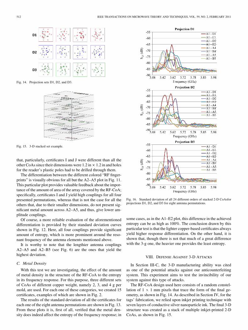
In Section III-C, the 3-D manufacturing ability was citedas one of the potential attacks against our anticounterfeitingsystem. This experiment aims to test the invincibility of oursystem against this type of attacks.
The RF-CoA design used here consists of a random constel-lation of 1 1 mm pixels that trace the form of the final ge-ometry, as shown in Fig. 14. As described in Section IV, for thetags’ fabrication, we relied upon inkjet printing technique withseven layers of conductive silver nanoparticle ink. The final 3-Dstructure was created as a stack of multiple inkjet-printed 2-DCoAs, as shown in Fig. 15.

LAKAFOSIS et al.: RF FINGERPRINTING PHYSICAL OBJECTS FOR ANTICOUNTERFEITING APPLICATIONS 513
In particular, what we have compared is the near-fieldresponse of three different-ordered stacked sets of the sameRF-CoA instances, namely, D1, D2, and D3, shown in Fig. 14.
For each set, 24 different orders of stacked 2-D CoAs havebeen measured and their standard deviation curves are shownin Fig. 16 for each of eight antenna permutations. The resultsindicate that there is significant variation in the near-field forthe different permutations, again especially around the resonantfrequency of the antenna elements. This ensures that even slightvariations in manufacturing in the -axis, i.e., thickness, willproduce distinct enough “RF fingerprints.”
IX. CONCLUSION
A high-performing robust standalone reader for anticounter-feiting applications, which is smaller, computationally morepowerful, and more accurate than its predecessor [12], has beendesigned and fabricated. The RF characterization of all compo-nents comprising the reader with an emphasis on accuracy andinsertion loss introduced has been done. The algorithm behindits fast and accurate MCU-assisted “RF fingerprint” extractionhas been described in detail.
As a means to verify the reader’s performance in extractingthe near-field frequency response of the RF-CoA physical struc-tures, a number of tests, namely, uniqueness among differentinstances, repeatability robustness for same instances, variationin conductive material density of the certificate, and 2-D to 3-Dprojection attacks have been conducted yielding very promisingresults.
This paper has demonstrated in the most straightforwardmanner that uniquely authenticated “super” RFID tags, in theform of badges of a small dielectric profile (e.g., 2 mm, foralignment purposes with the presented RF-CoA reader) directlyaffixed onto objects or in the form of carefully attached producttags, can prove a valuable tool against the ever-increasingaction of counterfeiters.
REFERENCES
[1] M. Robyn, “Market-driven fraud: The impact and consequences ofcounterfeit products and intellectual property violations,” presented atthe ASC Annu. Meeting, St. Louis, MO, Nov. 2008.
[2] “Seventh annual global software piracy study,” Business Softw. Al-liance, Washington, DC, 2009. [Online]. Available: http://portal.bsa.org/globalpiracy2009/studies/globalpiracystudy2009.pdf
[3] “Counterfeiting report,” Glaxo-Smith-Kline, Middlesex, U.K., 2009.[Online]. Available: http://www.gsk.com/responsibility/supply-chain/counterfeiting.htm
[4] Firewall protection for paper documents,” CrossID Inc., Hauppauge,NY, 2004. [Online]. Available: http://www.rfidjournal.com/article/ar-ticleview/790/1/44
[5] J. Collins, “RFID fibers for secure applications,” RFID J. 2004[Online]. Available: http://www.rfidjournal.com/article/article-view/845/1/14
[6] S. Preradovic and N. C. Karmakar, “Design of fully printable chiplessRFID tag on flexible substrate for secure banknote applications,” in 3rdInt. Anti-Counterfeiting, Security, Identification Commun. Conf., Aug.2009, pp. 206–210.
[7] L. Tsang et al., Theory of Microwave Remote Sensing. New York:Wiley, 1985.
[8] C. M. Gutierrez and P. Gallagher, “Secure hash standard,” Fed. Inform.Process. Standards, Gaithersburg, MD, FIPS PUB 180-3, Oct. 2008.
[9] R. Rivest, A. Shamir, and L. Adleman, “A method for obtaining digitalsignatures and public-key cryptosystems,” Commun. ACM, vol. 21, no.2, pp. 120–126, 1978.
[10] R. L. Li, G. DeJean, M. M. Tentzeris, and J. Laskar, “Development andanalysis of a folded shorted-patch antenna with reduced size,” IEEETrans. Antennas Propag., vol. 52, no. 2, pp. 555–562, Feb. 2004.
[11] “GaAsmmIC SP4T non-reflective positive control switch, DC—8GHz,” Hittite, Chelmsford, MA, 2008. [Online]. Available: www.hit-tite.com/content/documents/data_sheet/hmc345lp3.pdf
[12] V. Lakafosis, A. Traille, H. Lee, G. Orecchini, E. Gebara, M. M.Tentzeris, G. DeJean, and D. Kirovski, “An RFID system withenhanced hardware-enabled authentication and anti-counterfeitingcapabilities,” in IEEE MTT-S Int. Microw. Symp. Dig., Anaheim, CA,Jun. 2010, pp. 840–843.
[13] “mmIC VCO with buffer amplifier, 5.0–5.5 GHz,” Hittite, Chelmsford,MA, 2008. [Online]. Available: www.hittite.com/content/documents/data_sheet/hmc430lp4.pdf
[14] “mmIC VCO with buffer amplifier, 5.5–6.1 GHz,” Hittite, Chelmsford,MA, 2008. [Online]. Available: www.hittite.com/content/documents/data_sheet/hmc431lp4.pdf
[15] “MSP-EXP430F5438 Experimenter Board User’s Guide (Rev. D),”Texas Instruments Incorporated, Dallas, TX, Dec. 2009.
[16] “General purpose amplifier,” RFMD, Greensboro, NC, 2006. [Online].Available: www.rfmd.com/CS/Documents/3378DS.pdf
[17] 6 GHz RMS power detector, linear,” Milpitas, CA, 2008. [Online].Available: cds.linear.com/docs/Datasheet/5581fa.pdf
[18] J. Blair, “Sine-fitting software for IEEE standards 1057 and 1241,” inProc. IEEE Instrum. Meas. Technol. Conf., Venice, Italy, May 1999,pp. 1504–1506.
[19] K. Hejn and A. Pacut, “Sine-wave parameters estimation—The secondsource of inaccuracy,” in Proc. 20th IEEE Instrum. Meas. Technol.Con-ference, May 2003, vol. 2, pp. 1328–1333.
Vasileios Lakafosis (S’07) received the Diplomadegree in electrical and computer engineering fromNational Technical University, Athens, Greece, in2006, the M.Sc. degree in electrical and computerengineering from the Georgia Institute of Tech-nology, Atlanta, in 2009, and is currently workingtoward the Ph.D. degree at the Georgia Institute ofTechnology.
He has authored or coauthored over 12 papers inpeer-reviewed journals and conference proceedingsand one book chapter. His research interests include
networking protocols in the areas of wireless mobile ad hoc, mesh, and sensornetworks. His research has currently been focused on single- and multihop wire-less localization techniques, delay-tolerant and opportunistic networks, and per-petual low-power network protocols.
Mr. Vasileios is also a member of the Association for Computing Machinery(ACM) and the Technical Chamber of Greece.
Anya Traille was born in Washington, DC, in 1982.She received the B.S. and M.S. degrees in elec-trical and computer engineering from the GeorgiaInstitute of Technology, Atlanta, in 2004 and 2009,respectively.
She is currently a Research Engineer with theSchool of Electrical and Computer Engineering, At-lanta, GA. From 2004 to 2007, she was a Full-TimeResearch Engineer with the Georgia Tech ResearchInstitute, Smyrna, GA. In 2008, she was a VisitingScholar with Imperial College, London, U.K. In
2009, she was a Visiting Researcher with Georgia Tech Ireland, Athlone,Ireland. In 2010, she was a Visiting Researcher with LAAS-CNRS, Toulouse,France. Her main areas of research include antenna arrays, waveguides, RFID,and liquid antennas for bio-signal monitoring in which she has organized andchaired numerous conference sessions.
Ms. Traille was the recipient/corecipient of the IEEE IGARSS 2009 StudentTravel Award, the ISAP 2007 Best Poster Paper Award, the Second Place BestPaper Award of the Georgia Institute of Technology Graduate Research Fair2006 and the Best Session Paper Award of IEEE ECTC 2010. She was also afinalist in the 2008 IEEE AP-S Best Student Paper Competition and a finalist inthe 2007 ACES Symposium Best Student Paper Competition.

514 IEEE TRANSACTIONS ON MICROWAVE THEORY AND TECHNIQUES, VOL. 59, NO. 2, FEBRUARY 2011
Hoseon Lee received the B.S. and M.S. degrees fromthe Georgia Institute of Technology, Atlanta, in 2002and 2005, respectively, and is currently working to-ward the Ph.D. degree in electrical engineering at theGeorgia Institute of Technology.
From 2006 to 2009, he was a naval officer and As-sistant Professor with the Republic of Korea (ROK)Naval Academy. His research interests includelow-cost organic solutions for radars, communi-cation, sensing and identification systems, inkjetprinting, and power scavenging for RF applications.
Edward Gebara (S’03–M’06) received the B.S.(with highest honors), M.S., and Ph.D. degreesin electrical and computer engineering from theGeorgia Institute of Technology, Atlanta, in 1996,1999 and 2003, respectively.
From 1999 to 2000, he was an Invited Scientistwith Chalmers University, Göteborg, Sweden. In2001, he applied the results of his research to definethe core technology for Quellan Inc., as its initialemployee, which is now part of Intersil (NASDQ:ISIL). These technologies served as the basis for
signal integrity solutions developed for the enterprise, video, storage, andwireless markets. While working with Quellan Inc., he maintained a researchfaculty position with the Georgia Institute of Technology, where he led theresearch efforts of the Mixed-Signal Team. In early 2008, he joined the GeorgiaInstitute of Technology on a full-time basis. Since 2003, he has supervised ninePh.D. students whose research focuses on equalization, crosstalk cancellation,and self-healing mixed signal techniques in pure CMOS. These technologiesare applied to next-generation optics and wired and wireless communicationsystems. He has authored or coauthored over 70 papers. He holds five patents.
Dr. Gebara is a reviewer for the IEEE International Symposium and Circuitsand Systems (ISCAS) and for the IEEE Microwave Theory and TechniquesSociety (IEEE MTT-S) International Microwave Symposium (IMS). He alsoserved as workshop and tutorial chair of the Technical Program for the 2008IEEE MTT-S IMS.
Manos M. Tentzeris (S’89–M’92–SM’03–F’10)received the Diploma degree in electrical and com-puter engineering (Magna Cum Laude) from theNational Technical University of Athens, Athens,Greece, and the M.S. and Ph.D. degrees in electricalengineering and computer science from The Univer-sity of Michigan at Ann Arbor.
He is currently a Professor with the School of Elec-trical and Computer Engineering, Georgia Instituteof Technology. He has authored or coauthored over370 papers in refereed journals and conference pro-
ceedings, five books, and 19 book chapters. He has helped develop academicprograms in highly integrated/multilayer packaging for rf and wireless appli-cations using ceramic and organic flexible materials, paper-based RFIDs andsensors, “green” electronics and power scavenging, nanotechnology applica-tions in RF, microwave microelectromechanical systems (MEMS), system-on-package (SOP)-integrated (ultra-wideband (UWB), mutliband, conformal) an-tennas and adaptive numerical electromagnetics (finite difference time domain(FDTD) multiresolution algorithms), and heads the ATHENA Research Group(20 researchers). He is an Associate Editor for the International Journal on An-tennas and Propagation.
Dr. Tentzeris is a member of URSI Commission D and the MTT-15 Com-mittee. He is an associate member of the European Microwave Association(EuMA). He is a Fellow of the Electromagnetic Academy. He is a memberof the Technical Chamber of Greece. He is one of the IEEE MicrowaveTheory and Techniques Society (IEEE MTT-S) Distinguished MicrowaveLecturers (2010–2012). He is an associate editor of the IEEE TRANSACTIONS
ON MICROWAVE THEORY AND TECHNIQUES and the IEEE TRANSACTIONS ON
ADVANCED PACKAGING He has given more than 100 invited talks to variousuniversities and companies all over the world. He is the vice-chair of the RFTechnical Committee (TC16) of the IEEE CPMT Society. He is the founderand chair of the RFID Technical Committee (TC24) of the IEEE MTT-S andthe secretary/treasurer of the IEEE C-RFID. He was the recipient/corecipientof the 2010 IEEE Antennas and Propagation Society Piergiorgio L. E. UslenghiLetters Prize Paper Award, the 2010 Georgia Tech Senior Faculty OutstandingUndergraduate Research Mentor Award, the 2009 E. T. S. Walton Award fromthe Irish Science Foundation, the 2006 IEEE MTT-S Outstanding Young Engi-neer Award, the 2003 NASA Godfrey “Art” Anzic Collaborative DistinguishedPublication Award, the 2003 IBC International Educator of the Year Award,the 2003 IEEE CPMT Outstanding Young Engineer Award, the 2002 GeorgiaTech Electrical and Computer Engineering (ECE) Outstanding Junior FacultyAward, and the 2000 National Science Foundation (NSF) CAREER Award.
Gerald R. DeJean (S’03–M’06) received the B.S.degree in electrical and computer engineering (SumaCum Laude) from Michigan State University, EastLansing, in 2000, and the M.S. and Ph.D. degrees inelectrical and computer engineering from the GeorgiaInstitute of Technology, Atlanta, in 2005 and 2007,respectively.
He is currently a Researcher with Microsoft Re-search, Redmond, MA, where he is involved in thefield of RF design. He has authored or coauthoredover 40 papers in refereed journals and conference
proceedings. He has been involved in a number of research projects as a memberof the National Science Foundation (NSF) Packaging Research Center and theGeorgia Electronic Design Center. His research interests include antenna de-sign, RF/microwave design and characterization, and 3-D system-on-package(SOP) integration of embedded functions that focuses largely on modern com-mercial RF systems such as cellular phones for personal communications system(PCS) applications, Bluetooth and 2.4-GHz industrial–scientific–medical (ISM)applications, RFIDs, WLAN (802.11a,b,g), LMDS, and millimeter-wave ap-plications at 60 GHz. He has dedicated his research to making the antennamore compact and integrable with multilayer packages such as low-temperaturecofired ceramic (LTCC), liquid crystal polymer (LCP), and multilayer organic(MLO), while maintaining the full functionality of the device for widebandand/or multiband applications. He is also interested in equivalent circuit mod-eling techniques to assist in the design and optimization of compact antennas.
Dr. DeJean is a member of Eta Kappa Nu and Tau Beta Pi. He was the re-cipient of the Microsoft Research Fellowship Award for excellence in graduateresearch. He was twice a finalist of the Student Paper Competition of the 2004and 2005 IEEE Antennas and Propagation Society Symposia.
Darko Kirovski (M’09) received the Ph.D. degree incomputer science from the University of California atLos Angeles (UCLA), in 2001.
Since joining Microsoft Research, Redmond,WA, in 2000, he has split time between the Cryptoand Machine Learning Groups, during which timehe has been involved on a wide variety of systemprojects that span authentication, anticounterfeiting,and XBOX Kinect games, among others. He hascoauthored over 100 conference and journal papers.His inventions have been recorded in over 70 patent
filings.Dr. Kirovski is involved with the IEEE Information Forensics and Security
Subdivision, Signal Processing Society (SPS). He was the recipient of severalawards, including the 2001 Association for Computing Machinery (ACM)/IEEEOutstanding Ph.D. Dissertation in Electronic Design Automation, the MicrosoftGraduate Fellowship, and the ACM Multimedia Best Paper Award.