Results of new CD detection capability on advanced reticles
10
Results of new CD detection capability on advanced reticles Arosha Goonesekera 1 , Heiko Schmalfuss 1 , Isaac Lee 1 , Chun Guan 1 , Aditya Dayal 1 Thomas Schulmeyer 2 , Jan Heumann 2 1 KLA-Tencor Corporation, 160 Rio Robles, San Jose, CA 95134, USA 2 Advanced Mask Technology Center, Postfach 11 01 61, D-01330, Dresden, Germany ABSTRACT Semiconductor device manufacturers have made technological advances in fabricating devices at 65nm and 45nm nodes. Technology is advancing towards 32nm node devices. Reticles at these device nodes are designed with tight critical dimension (CD) specifications and sub-resolution features. Inspection tools capable of detecting CD defects on the order of 20 nm are required to accommodate these device nodes. To meet this challenge, KLA-Tencor has developed a new “CD Detector” capability on the TeraScanHR reticle inspection tool that efficiently detects two-sided CD defects on reticles at the 45nm node and beyond. The CD Detector is available in both Die-to-Die (DD) and Die-to-Database (DB) inspection modes. This paper presents results of a CD Detector Beta evaluation on variety of advanced reticles in a production setting at Advanced Mask Technology Center (AMTC) in Germany. Inspection results will demonstrate improved sensitivity to two-sided CD defects and good inspectability, at inspection times similar to a standard HiRes inspection. Discussion will focus on enabling the highest sensitivity to CD defects at 72nm pixel inspections, which is suitable for advanced research and development studies, as well as improved sensitivity at 90nm pixel inspections for higher productivity. 1. INTRODUCTION Optical lithography technology has progressed rapidly in recent years with the use of dramatically reduced design rules. This trend can be seen in smaller main features and linewidths as well as the incorporation of novel resolution enhancement techniques (RET). These RET, such as phase shift masks, optical proximity correction (OPC) features and sub-resolution assist features (SRAF) allow lithographers to print smaller critical features on the wafer with tighter critical dimension (CD) control 1,2 . The use of RET accompanied by smaller features on a reticle has impacted reticle inspection in a number of ways. Primarily, it requires aggressive improvements in the spatial resolution of new generation inspection tools to accommodate shrinking primary feature sizes. The improvement in spatial resolution is coupled to a quadratic increase in the total number of pixels that the inspection system must process for a given inspection area on the photomask. In addition, there has been a substantial increase in the number of the smallest structures that require inspection due to widespread use of OPC and SRAF. These attributes impose tighter requirements on an inspection system’s ability to find real defects while keeping false detection rates below one part in 10 10 (assuming a 120mm × 120mm inspection area, a 90nm inspection pixel size and less than 100 defective pixels in a single inspection). Another issue is the complexity of the processing steps for fabrication of advanced reticles that has introduced new classes of process-related reticle defects that require detection, as well as the economically driven necessity to detect these defects early in the processing stage when a reticle can be re-worked. Any successful reticle inspection methodology requires that an inspection tool be capable of inspecting a variety of production reticles while providing adequate sensitivity for the particular layer and technology node, while handling small geometries, finding the smallest defects that potentially Photomask and Next-Generation Lithography Mask Technology XV, edited by Toshiyuki Horiuchi, Proc. of SPIE Vol. 7028, 70282L, (2008) 0277-786X/08/$18 · doi: 10.1117/12.793091 Proc. of SPIE Vol. 7028 70282L-1
Transcript of Results of new CD detection capability on advanced reticles
Results of new CD detection capability on advanced reticles
Arosha Goonesekera1, Heiko Schmalfuss1, Isaac Lee1, Chun Guan1, Aditya Dayal1 Thomas Schulmeyer2, Jan Heumann2
1KLA-Tencor Corporation, 160 Rio Robles, San Jose, CA 95134, USA 2Advanced Mask Technology Center, Postfach 11 01 61, D-01330, Dresden, Germany
ABSTRACT
Semiconductor device manufacturers have made technological advances in fabricating devices at 65nm and 45nm nodes. Technology is advancing towards 32nm node devices. Reticles at these device nodes are designed with tight critical dimension (CD) specifications and sub-resolution features. Inspection tools capable of detecting CD defects on the order of 20 nm are required to accommodate these device nodes. To meet this challenge, KLA-Tencor has developed a new “CD Detector” capability on the TeraScanHR reticle inspection tool that efficiently detects two-sided CD defects on reticles at the 45nm node and beyond. The CD Detector is available in both Die-to-Die (DD) and Die-to-Database (DB) inspection modes. This paper presents results of a CD Detector Beta evaluation on variety of advanced reticles in a production setting at Advanced Mask Technology Center (AMTC) in Germany. Inspection results will demonstrate improved sensitivity to two-sided CD defects and good inspectability, at inspection times similar to a standard HiRes inspection. Discussion will focus on enabling the highest sensitivity to CD defects at 72nm pixel inspections, which is suitable for advanced research and development studies, as well as improved sensitivity at 90nm pixel inspections for higher productivity.
1. INTRODUCTION Optical lithography technology has progressed rapidly in recent years with the use of dramatically reduced design rules. This trend can be seen in smaller main features and linewidths as well as the incorporation of novel resolution enhancement techniques (RET). These RET, such as phase shift masks, optical proximity correction (OPC) features and sub-resolution assist features (SRAF) allow lithographers to print smaller critical features on the wafer with tighter critical dimension (CD) control1,2. The use of RET accompanied by smaller features on a reticle has impacted reticle inspection in a number of ways. Primarily, it requires aggressive improvements in the spatial resolution of new generation inspection tools to accommodate shrinking primary feature sizes. The improvement in spatial resolution is coupled to a quadratic increase in the total number of pixels that the inspection system must process for a given inspection area on the photomask. In addition, there has been a substantial increase in the number of the smallest structures that require inspection due to widespread use of OPC and SRAF. These attributes impose tighter requirements on an inspection system’s ability to find real defects while keeping false detection rates below one part in 1010 (assuming a 120mm × 120mm inspection area, a 90nm inspection pixel size and less than 100 defective pixels in a single inspection). Another issue is the complexity of the processing steps for fabrication of advanced reticles that has introduced new classes of process-related reticle defects that require detection, as well as the economically driven necessity to detect these defects early in the processing stage when a reticle can be re-worked. Any successful reticle inspection methodology requires that an inspection tool be capable of inspecting a variety of production reticles while providing adequate sensitivity for the particular layer and technology node, while handling small geometries, finding the smallest defects that potentially
Photomask and Next-Generation Lithography Mask Technology XV,edited by Toshiyuki Horiuchi, Proc. of SPIE Vol. 7028, 70282L, (2008)
0277-786X/08/$18 · doi: 10.1117/12.793091
Proc. of SPIE Vol. 7028 70282L-1
impact a device, maintaining high defect capture rates on highly transparent films, and dealing with decreased contrast on SRAF2.
The new CD-detector (CDD) algorithm addresses the requirement of improved sensitivity to capturing defects on small geometries present in all new advanced reticles 65 nm node and beyond. It has been developed on the KLA-Tencor TeraScanHR reticle inspection platform, in which the light source is a 257nm continuous wave laser3,4. It improves the sensitivity by a factor of 2 for two-sided critical dimensional defects (CD-errors) over the previous best capability, without any modifications to the optical resolution of the tool. The present imaging system of the TeraScanHR platform allows the choice of three out of the following four pixel sizes: 72nm, 90nm, 125nm, and 150nm, hereafter referred to as p72, p90, p125 and p150 respectively. As for any imaging system, the move to a larger Numerical Aperture (or smaller pixel) results in a reduced depth of focus. The TeraScanHR platform includes an advanced autofocus subsystem (AF2) which provides the necessary precision to compensate for the reduced depth of focus. The new AF2 uses an advanced pre-mapping technique (Z-calibration) which has improved focus capability on all types of reticles 4. Section 2 presents an overview of the CD detector algorithm and its capabilities. The results of the engineering and alpha test phase are discussed in section 3. The results of our beta testing at AMTC are presented in section 4 and section 5 summarizes the overall results.
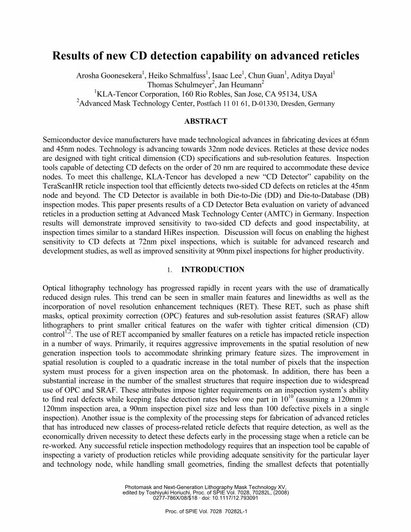
2. CD-DETECTOR ALGORITHM The CD-detector algorithm is designed to operate on both Die-to-Die (DD) and Die-to-Database (DB) modes of inspection that are currently available with the TeraScanHR reticle inspection platform. Die-to-Die inspections compare optical images collected from a test die to the optical images from a reference die while Die-to-Database inspections compare optical images collected from the reticle to a database-rendered reference image1. The CD detector is primarily designed to capture two-sided CD-errors on line/space layers and on contact layers. CD-errors of a two-sided nature can be symmetric or asymmetric as shown in Figure 1. The CD detector captures both kinds of CD-errors but the efficiency is higher for symmetric defects.
Figure 1: Typical two-sided CD-errors that CDD have the capability capture: (a) symmetric two-sided CD defect with respect to opaque line (b) asymmetric two-sided CD defect with respect to clear space.
(a) (b)
Proc. of SPIE Vol. 7028 70282L-2
(a) (b)
(e) if) (g)
(h) ProcessedTest image
1
(a) ProcessedReference image
(C) Edge Profile (3)
(1)
N(2)
(C) Captured CD defect
(d) Difference image
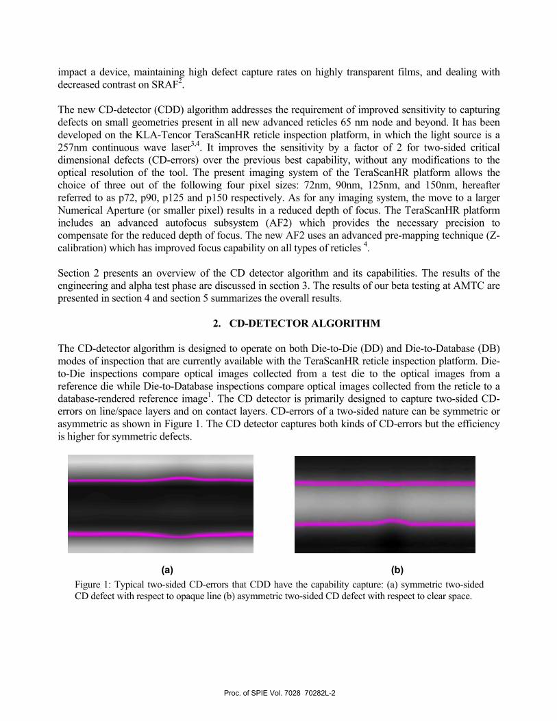
The defect types that the CD detector algorithm is capable of capturing are shown in Figure 2. There are three types each for opaque and clear structures; Line-Line, Line-LineEnd and LineEnd-LineEnd.
Figure. 2: CD detector defect types: (a) Clear Line-Line, (b) Clear Line-LineEnd, (c) Clear LineEnd-LineEnd, (d) Opaque Line-Line, (e) Opaque Line-LineEnd, (f) Opaque LineEnd-LineEnd
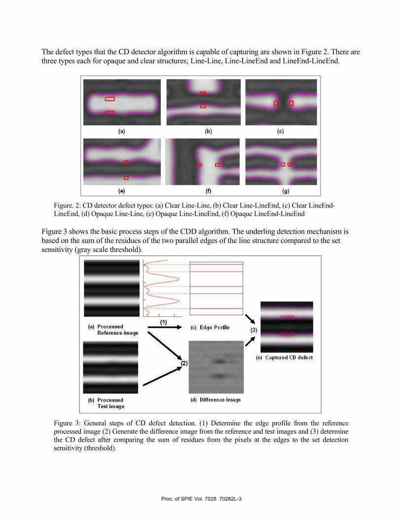
Figure 3 shows the basic process steps of the CDD algorithm. The underling detection mechanism is based on the sum of the residues of the two parallel edges of the line structure compared to the set sensitivity (gray scale threshold).
Figure 3: General steps of CD defect detection. (1) Determine the edge profile from the reference processed image (2) Generate the difference image from the reference and test images and (3) determine the CD defect after comparing the sum of residues from the pixels at the edges to the set detection sensitivity (threshold).
Proc. of SPIE Vol. 7028 70282L-3
300 — _______ ________________P72
P90
£
100 _______________• (G) DDT-P72• (H) DDT-P72
50 -A (G) DDT-P90
• (H) DDT-P90
0-10 15 20 25 30 35 40 45 50
Defect size (nm)
200
Set threshold
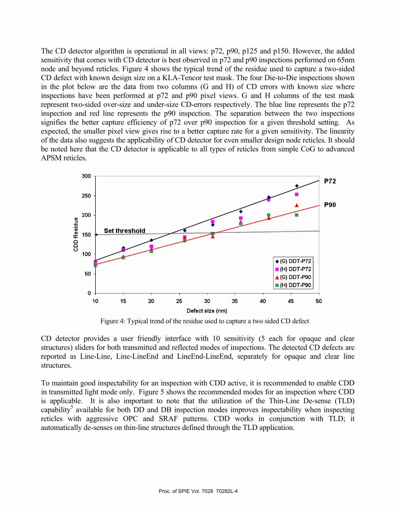
The CD detector algorithm is operational in all views: p72, p90, p125 and p150. However, the added sensitivity that comes with CD detector is best observed in p72 and p90 inspections performed on 65nm node and beyond reticles. Figure 4 shows the typical trend of the residue used to capture a two-sided CD defect with known design size on a KLA-Tencor test mask. The four Die-to-Die inspections shown in the plot below are the data from two columns (G and H) of CD errors with known size where inspections have been performed at p72 and p90 pixel views. G and H columns of the test mask represent two-sided over-size and under-size CD-errors respectively. The blue line represents the p72 inspection and red line represents the p90 inspection. The separation between the two inspections signifies the better capture efficiency of p72 over p90 inspection for a given threshold setting. As expected, the smaller pixel view gives rise to a better capture rate for a given sensitivity. The linearity of the data also suggests the applicability of CD detector for even smaller design node reticles. It should be noted here that the CD detector is applicable to all types of reticles from simple CoG to advanced APSM reticles.
Figure 4: Typical trend of the residue used to capture a two sided CD defect
CD detector provides a user friendly interface with 10 sensitivity (5 each for opaque and clear structures) sliders for both transmitted and reflected modes of inspections. The detected CD defects are reported as Line-Line, Line-LineEnd and LineEnd-LineEnd, separately for opaque and clear line structures.
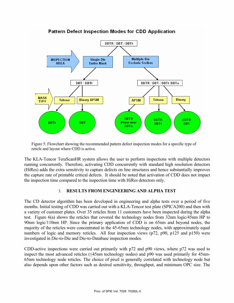
To maintain good inspectability for an inspection with CDD active, it is recommended to enable CDD in transmitted light mode only. Figure 5 shows the recommended modes for an inspection where CDD is applicable. It is also important to note that the utilization of the Thin-Line De-sense (TLD) capability5 available for both DD and DB inspection modes improves inspectability when inspecting reticles with aggressive OPC and SRAF patterns. CDD works in conjunction with TLD; it automatically de-senses on thin-line structures defined through the TLD application.
Proc. of SPIE Vol. 7028 70282L-4
Pattern Defect Inspection Modes for CDD Application
ON
lAs K[VP F
Figure 5: Flowchart showing the recommended pattern defect inspection modes for a specific type of reticle and layout where CDD is active.
The KLA-Tencor TeraScanHR system allows the user to perform inspections with multiple detectors running concurrently. Therefore, activating CDD concurrently with standard high resolution detectors (HiRes) adds the extra sensitivity to capture defects on line structures and hence substantially improves the capture rate of printable critical defects. It should be noted that activation of CDD does not impact the inspection time compared to the inspection time with HiRes detectors only.
3. RESULTS FROM ENGINEERING AND ALPHA TEST
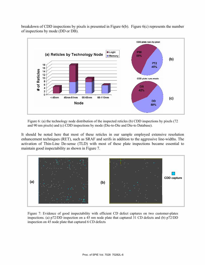
The CD detector algorithm has been developed in engineering and alpha tests over a period of five months. Initial testing of CDD was carried out with a KLA-Tencor test plate (SPICA200) and then with a variety of customer plates. Over 35 reticles from 11 customers have been inspected during the alpha test. Figure 6(a) shows the reticles that covered the technology nodes from 32nm logic/45nm HP to 90nm logic/110nm HP. Since the primary application of CDD is on 65nm and beyond nodes, the majority of the reticles were concentrated in the 45-65nm technology nodes, with approximately equal numbers of logic and memory reticles. All four inspection views (p72, p90, p125 and p150) were investigated in Die-to-Die and Die-to-Database inspection modes.
CDD-active inspections were carried out primarily with p72 and p90 views, where p72 was used to inspect the most advanced reticles (≤45nm technology nodes) and p90 was used primarily for 45nm-65nm technology node reticles. The choice of pixel is generally correlated with technology node but also depends upon other factors such as desired sensitivity, throughput, and minimum OPC size. The
Proc. of SPIE Vol. 7028 70282L-5
CDD plate runs by pixel
CDD plate runs mode
.LogicReticles by Technology Node .Memory
18___Il)16
o 14ii l2z_____1oy____
<4Snm 4Snm-51 nm 66-6Snm 66-1 lOnm
Node
breakdown of CDD inspections by pixels is presented in Figure 6(b). Figure 6(c) represents the number of inspections by mode (DD or DB).
Figure 6: (a) the technology node distribution of the inspected reticles (b) CDD inspections by pixels (72 and 90 nm pixels) and (c) CDD inspections by mode (Die-to-Die and Die-to Database).
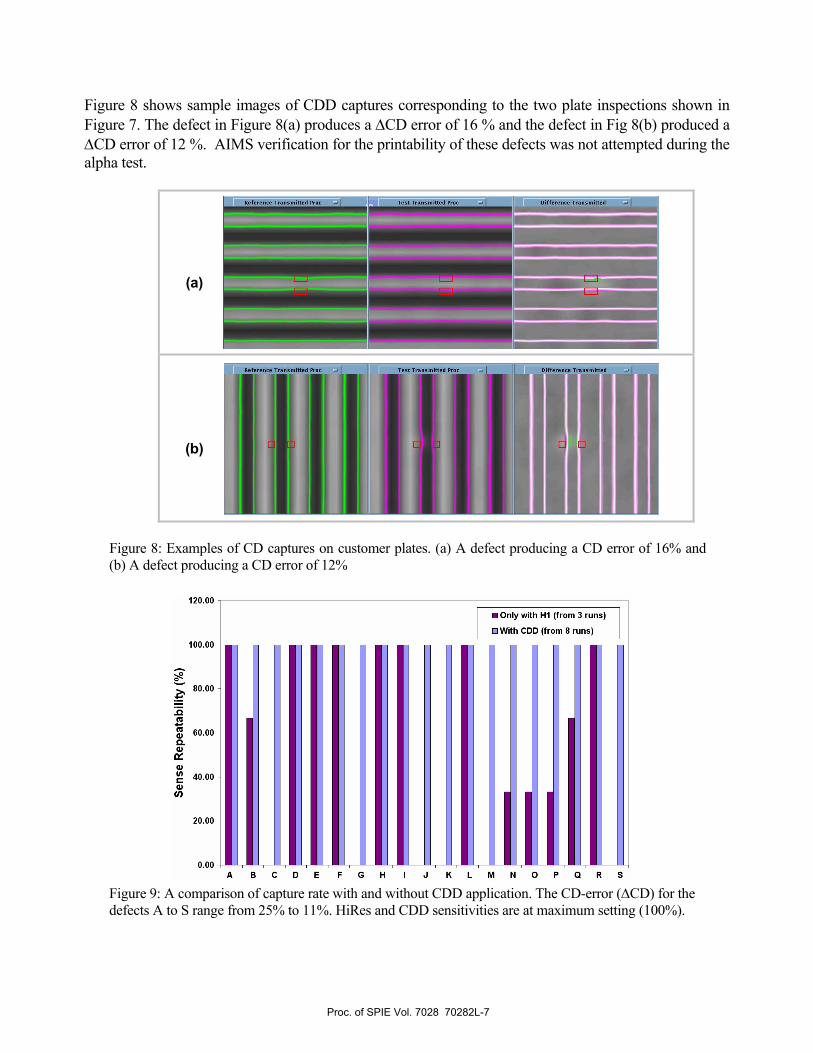
It should be noted here that most of these reticles in our sample employed extensive resolution enhancement techniques (RET), such as SRAF and serifs in addition to the aggressive line-widths. The activation of Thin-Line De-sense (TLD) with most of these plate inspections became essential to maintain good inspectability as shown in Figure 7.
Figure 7: Evidence of good inspectability with efficient CD defect captures on two customer-plates inspections. (a) p72/DD inspection on a 45 nm node plate that captured 31 CD defects and (b) p72/DD inspection on 45 node plate that captured 6 CD defects
(a) (b)
(c)
(a) (b) CDD capture
Proc. of SPIE Vol. 7028 70282L-6
Refereoce Troosloiffed Proc TesS Troosmiffed Proc
101011 III
• Only with HI (from 3 runs)
LI With CDD (from 8 runs)
120.00
100.00
80.00
60.00
40.00
20.00
0.00 A B C D E F G H I J K L M N 0 P Q R S
Figure 8 shows sample images of CDD captures corresponding to the two plate inspections shown in Figure 7. The defect in Figure 8(a) produces a ∆CD error of 16 % and the defect in Fig 8(b) produced a ∆CD error of 12 %. AIMS verification for the printability of these defects was not attempted during the alpha test.
Figure 8: Examples of CD captures on customer plates. (a) A defect producing a CD error of 16% and (b) A defect producing a CD error of 12%
Figure 9: A comparison of capture rate with and without CDD application. The CD-error (∆CD) for the defects A to S range from 25% to 11%. HiRes and CDD sensitivities are at maximum setting (100%).
(a)
(b)
Proc. of SPIE Vol. 7028 70282L-7
03a0.34-- 0320-2023-020024-0 220.20 - I S0.10-012-0120_I0-08•0_OS-0 02
0.43
a a arroltle (microns at mask)
Figure 9 shows another example of CDD capability tested on a programmed defect plate. The chart indicates a dramatic improvement in capture rate with excellent repeatability (100%) for inspections with CDD along with standard HiRes detectors. Note that many of these defects (C, G, J, K, M and S) were unique captures by CDD only.
4. RESULTS FROM BETA TEST
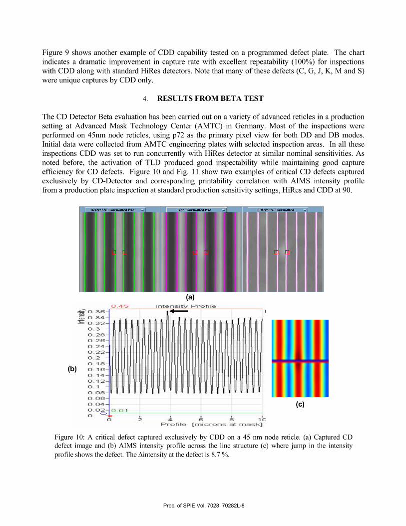
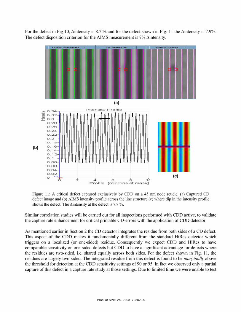
The CD Detector Beta evaluation has been carried out on a variety of advanced reticles in a production setting at Advanced Mask Technology Center (AMTC) in Germany. Most of the inspections were performed on 45nm node reticles, using p72 as the primary pixel view for both DD and DB modes. Initial data were collected from AMTC engineering plates with selected inspection areas. In all these inspections CDD was set to run concurrently with HiRes detector at similar nominal sensitivities. As noted before, the activation of TLD produced good inspectability while maintaining good capture efficiency for CD defects. Figure 10 and Fig. 11 show two examples of critical CD defects captured exclusively by CD-Detector and corresponding printability correlation with AIMS intensity profile from a production plate inspection at standard production sensitivity settings, HiRes and CDD at 90.
Figure 10: A critical defect captured exclusively by CDD on a 45 nm node reticle. (a) Captured CD defect image and (b) AIMS intensity profile across the line structure (c) where jump in the intensity profile shows the defect. The ∆intensity at the defect is 8.7 %.
(a)
(b)
(c)
Proc. of SPIE Vol. 7028 70282L-8
I I Ia 6 8 icRrofi le [microns at masFc]
Intensity RrofiIe0
- 0_a00
000_0-000_000
For the defect in Fig 10, ∆intensity is 8.7 % and for the defect shown in Fig: 11 the ∆intensity is 7.9%. The defect disposition criterion for the AIMS measurement is 7% ∆intensity.
Figure 11: A critical defect captured exclusively by CDD on a 45 nm node reticle. (a) Captured CD defect image and (b) AIMS intensity profile across the line structure (c) where dip in the intensity profile shows the defect. The ∆intensity at the defect is 7.8 %.
Similar correlation studies will be carried out for all inspections performed with CDD active, to validate the capture rate enhancement for critical printable CD-errors with the application of CDD detector. As mentioned earlier in Section 2 the CD detector integrates the residue from both sides of a CD defect. This aspect of the CDD makes it fundamentally different from the standard HiRes detector which triggers on a localized (or one-sided) residue. Consequently we expect CDD and HiRes to have comparable sensitivity on one-sided defects but CDD to have a significant advantage for defects where the residues are two-sided, i.e. shared equally across both sides. For the defect shown in Fig. 11, the residues are largely two-sided. The integrated residue from this defect is found to be marginally above the threshold for detection at the CDD sensitivity settings of 90 or 95. In fact we observed only a partial capture of this defect in a capture rate study at those settings. Due to limited time we were unable to test
(a)
(c)
(b)
Proc. of SPIE Vol. 7028 70282L-9
capture rate at a CDD slider setting of 100. In contrast the residues from each side are 20-60% below the HiRes detection threshold, showing clearly that this type of defect requires CDD at high setting for detection. The chart in Fig. 9 illustrates the advantage of CDD over HiRes for such types of defects as well.
5. SUMMARY Reticles made with 65 nm and beyond device nodes have been designed with tight critical dimension (CD) specifications and sub-resolution features. Inspection tools capable of detecting CD defects on the order of 20 nm are required to accommodate the challenge presented to the mask inspection technology. The new CD detector developed on the KLA-Tencor TeraScanHR reticle inspection platform provides this capability through efficient detection of two-sided CD defects. The CD Detector functionality is available in both Die-to-Die (DD) and Die-to-Database (DB) inspection modes. Inspection results carried out during alpha and beta phases demonstrate the improved sensitivity to two-sided CD defects and good inspectability, at inspection times similar to a standard HiRes inspection.
ACKNOWLEDGEMENTS
The authors would like to acknowledge Advanced Mask Technology Center (AMTC) in Germany for the participation of Beta phase testing and useful discussions on this paper with Michael Lang of KLA-Tencor.
REFERENCES [1] Dayal, A., Sier, J., Sousa, W., Labovitz, S., “Optimized inspection of advance reticles on the TeraScan reticle inspection tool,” Proc. SPIE 5992, 599245 (2005). [2] Eynon, B. G., Wu, B., [Photomask Fabrication Technology], McGraw Hill Professional, New York, 373-375 (2005). [3] Sier, J., Broadbent, W., Mirzaagha, F., Yu, P., “Inspection results for 32nm logic and sub-50nm half pitch memory reticles using the TeraScanHR,” Proc. SPIE 6730, 67302A (2007). [4] Broadbent, W., Yokoyama, I., Yu, P., Seki, K., Nomura, R., Schmalfuss, H., Heumann, J., Sier, J., “Field results from a new die-to-database reticle inspection platform,” Proc. SPIE 6607, 660714 (2007). [5] Chen, C., Kim, D., Park, K. H., Kim, N., Han, S. H., Park, J. H., Chung, D. H., “Improving inspectability with KLA-Tencor TeraScan thin line de-sense,” Proc. SPIE 6730, 67303O (2007).
Proc. of SPIE Vol. 7028 70282L-10