Diametrical Ring Size Listing Individual Ring Types and Set ...
Upload
khangminh22Category
view
0download
0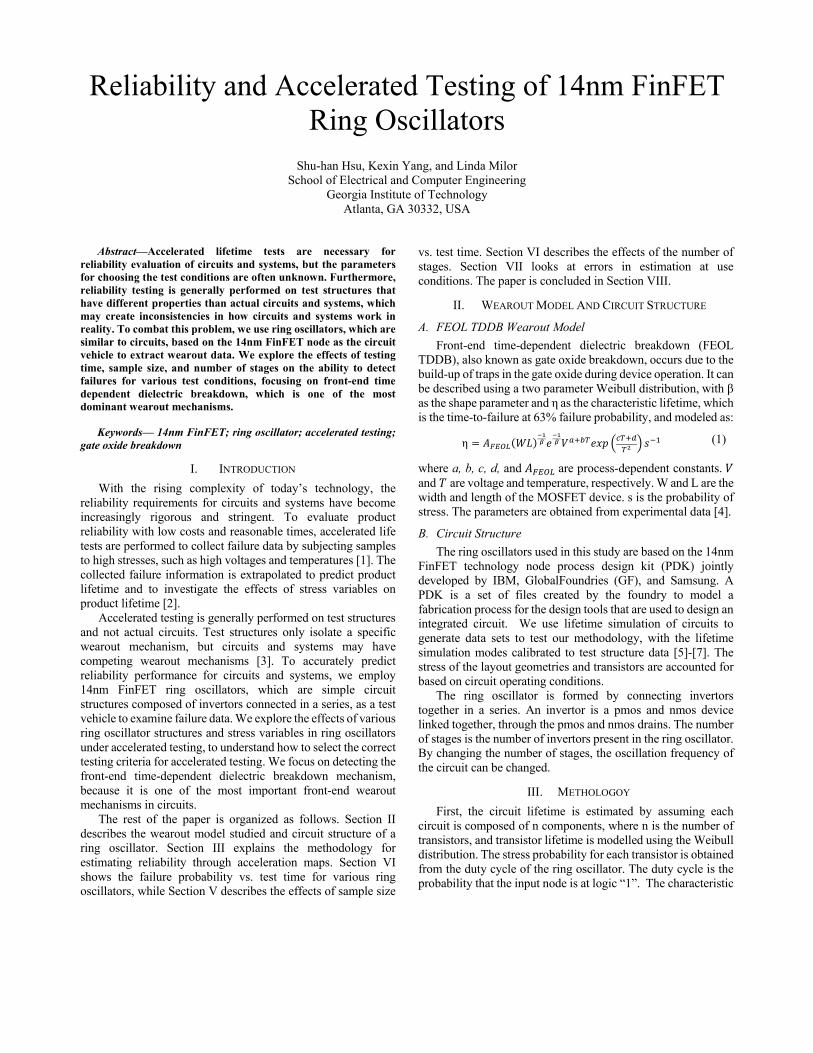
Reliability and Accelerated Testing of 14nm FinFET Ring Oscillators
Shu-han Hsu, Kexin Yang, and Linda Milor
School of Electrical and Computer Engineering Georgia Institute of Technology
Atlanta, GA 30332, USA
Abstract—Accelerated lifetime tests are necessary for
reliability evaluation of circuits and systems, but the parameters for choosing the test conditions are often unknown. Furthermore, reliability testing is generally performed on test structures that have different properties than actual circuits and systems, which may create inconsistencies in how circuits and systems work in reality. To combat this problem, we use ring oscillators, which are similar to circuits, based on the 14nm FinFET node as the circuit vehicle to extract wearout data. We explore the effects of testing time, sample size, and number of stages on the ability to detect failures for various test conditions, focusing on front-end time dependent dielectric breakdown, which is one of the most dominant wearout mechanisms.
Keywords— 14nm FinFET; ring oscillator; accelerated testing; gate oxide breakdown
I. INTRODUCTION
With the rising complexity of today’s technology, the reliability requirements for circuits and systems have become increasingly rigorous and stringent. To evaluate product reliability with low costs and reasonable times, accelerated life tests are performed to collect failure data by subjecting samples to high stresses, such as high voltages and temperatures [1]. The collected failure information is extrapolated to predict product lifetime and to investigate the effects of stress variables on product lifetime [2].
Accelerated testing is generally performed on test structures and not actual circuits. Test structures only isolate a specific wearout mechanism, but circuits and systems may have competing wearout mechanisms [3]. To accurately predict reliability performance for circuits and systems, we employ 14nm FinFET ring oscillators, which are simple circuit structures composed of invertors connected in a series, as a test vehicle to examine failure data. We explore the effects of various ring oscillator structures and stress variables in ring oscillators under accelerated testing, to understand how to select the correct testing criteria for accelerated testing. We focus on detecting the front-end time-dependent dielectric breakdown mechanism, because it is one of the most important front-end wearout mechanisms in circuits.
The rest of the paper is organized as follows. Section II describes the wearout model studied and circuit structure of a ring oscillator. Section III explains the methodology for estimating reliability through acceleration maps. Section VI shows the failure probability vs. test time for various ring oscillators, while Section V describes the effects of sample size
vs. test time. Section VI describes the effects of the number of stages. Section VII looks at errors in estimation at use conditions. The paper is concluded in Section VIII.
II. WEAROUT MODEL AND CIRCUIT STRUCTURE
A. FEOL TDDB Wearout Model
Front-end time-dependent dielectric breakdown (FEOL TDDB), also known as gate oxide breakdown, occurs due to the build-up of traps in the gate oxide during device operation. It can be described using a two parameter Weibull distribution, with β as the shape parameter and η as the characteristic lifetime, which is the time-to-failure at 63% failure probability, and modeled as:
η (1)
where a, b, c, d, and are process-dependent constants. and are voltage and temperature, respectively. W and L are the width and length of the MOSFET device. s is the probability of stress. The parameters are obtained from experimental data [4].
B. Circuit Structure
The ring oscillators used in this study are based on the 14nm FinFET technology node process design kit (PDK) jointly developed by IBM, GlobalFoundries (GF), and Samsung. A PDK is a set of files created by the foundry to model a fabrication process for the design tools that are used to design an integrated circuit. We use lifetime simulation of circuits to generate data sets to test our methodology, with the lifetime simulation modes calibrated to test structure data [5]-[7]. The stress of the layout geometries and transistors are accounted for based on circuit operating conditions. The ring oscillator is formed by connecting invertors together in a series. An invertor is a pmos and nmos device linked together, through the pmos and nmos drains. The number of stages is the number of invertors present in the ring oscillator. By changing the number of stages, the oscillation frequency of the circuit can be changed.
III. METHOLOGOY
First, the circuit lifetime is estimated by assuming each circuit is composed of n components, where n is the number of transistors, and transistor lifetime is modelled using the Weibull distribution. The stress probability for each transistor is obtained from the duty cycle of the ring oscillator. The duty cycle is the probability that the input node is at logic “1”. The characteristic
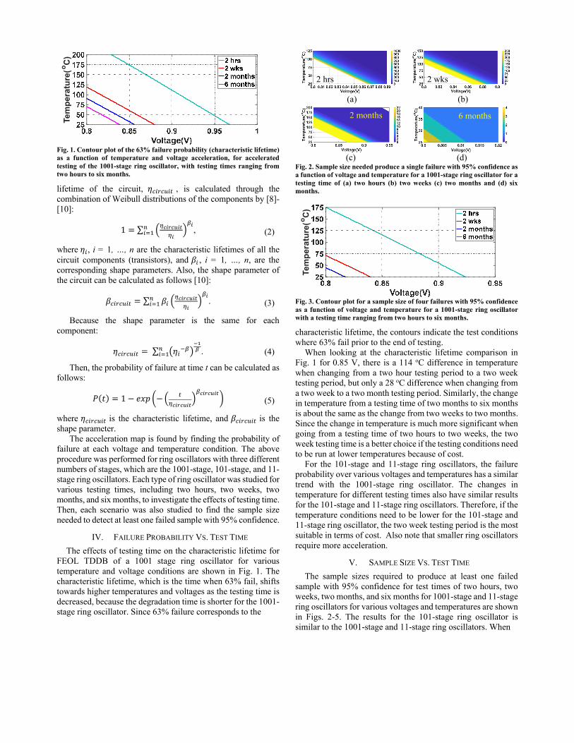
Fig. 1. Contour plot of the 63% failure probability (characteristic lifetime) as a function of temperature and voltage acceleration, for accelerated testing of the 1001-stage ring oscillator, with testing times ranging from two hours to six months.
lifetime of the circuit, , is calculated through the combination of Weibull distributions of the components by [8]-[10]:
1 ∑ , (2)
where , i = 1, …, n are the characteristic lifetimes of all the circuit components (transistors), and , i = 1, …, n, are the corresponding shape parameters. Also, the shape parameter of the circuit can be calculated as follows [10]:
∑ . (3)
Because the shape parameter is the same for each component:
∑ . (4)
Then, the probability of failure at time t can be calculated as follows:
1 (5)
where is the characteristic lifetime, and is the shape parameter. The acceleration map is found by finding the probability of failure at each voltage and temperature condition. The above procedure was performed for ring oscillators with three different numbers of stages, which are the 1001-stage, 101-stage, and 11-stage ring oscillators. Each type of ring oscillator was studied for various testing times, including two hours, two weeks, two months, and six months, to investigate the effects of testing time. Then, each scenario was also studied to find the sample size needed to detect at least one failed sample with 95% confidence.
IV. FAILURE PROBABILITY VS. TEST TIME
The effects of testing time on the characteristic lifetime for FEOL TDDB of a 1001 stage ring oscillator for various temperature and voltage conditions are shown in Fig. 1. The characteristic lifetime, which is the time when 63% fail, shifts towards higher temperatures and voltages as the testing time is decreased, because the degradation time is shorter for the 1001-stage ring oscillator. Since 63% failure corresponds to the
(a)
(b)
(c) (d) Fig. 2. Sample size needed produce a single failure with 95% confidence as a function of voltage and temperature for a 1001-stage ring oscillator for a testing time of (a) two hours (b) two weeks (c) two months and (d) six months.
Fig. 3. Contour plot for a sample size of four failures with 95% confidence as a function of voltage and temperature for a 1001-stage ring oscillator with a testing time ranging from two hours to six months.
characteristic lifetime, the contours indicate the test conditions where 63% fail prior to the end of testing.
When looking at the characteristic lifetime comparison in Fig. 1 for 0.85 V, there is a 114 oC difference in temperature when changing from a two hour testing period to a two week testing period, but only a 28 oC difference when changing from a two week to a two month testing period. Similarly, the change in temperature from a testing time of two months to six months is about the same as the change from two weeks to two months. Since the change in temperature is much more significant when going from a testing time of two hours to two weeks, the two week testing time is a better choice if the testing conditions need to be run at lower temperatures because of cost.
For the 101-stage and 11-stage ring oscillators, the failure probability over various voltages and temperatures has a similar trend with the 1001-stage ring oscillator. The changes in temperature for different testing times also have similar results for the 101-stage and 11-stage ring oscillators. Therefore, if the temperature conditions need to be lower for the 101-stage and 11-stage ring oscillator, the two week testing period is the most suitable in terms of cost. Also note that smaller ring oscillators require more acceleration.
V. SAMPLE SIZE VS. TEST TIME
The sample sizes required to produce at least one failed sample with 95% confidence for test times of two hours, two weeks, two months, and six months for 1001-stage and 11-stage ring oscillators for various voltages and temperatures are shown in Figs. 2-5. The results for the 101-stage ring oscillator is similar to the 1001-stage and 11-stage ring oscillators. When
Tem
per
atu
re(o
C)
Tem
per
atu
re(o
C)
2 hrs 2 wks
2 months 6 months

(a)
(b)
(c) (d) Fig. 4. Sample size needed produce a single failure with 95% confidence as a function of voltage and temperature for a 11-stage ring oscillator for a testing time of (a) two hours (b) two weeks (c) two months and (d) six months.
Fig. 5. Contour plot for a sample size of four failures with 95% confidence as a function of voltage and temperature for a 11-stage ring oscillator with a testing time ranging from two hours to six months.
comparing the failure probabilities to the sample sizes, the high voltage and temperature regions only require a sample size of 1 to detect at least one failure due to the failure probability being 100%. However, as the temperatures and voltages are decreased, the increase in sample size needed for a 95% confidence level increases by three orders of magnitude for a two hour testing time, whereas the sample size increase is only one order of magnitude when the testing time is longer at six months.
The change in temperature conditions at fixed voltages for the same sample size for each type of ring oscillator for various testing times follows the same trend as the characteristic lifetime. For both ring oscillators, there is a significant difference in the voltage for the required sample size at a 95% confidence level when changing from a two hour to a two week testing period, but a much smaller difference when changing from a two week to a two month testing period, as well as from a two month to a six month testing period. Therefore, the two week testing period is also optimal when considering the required sample size to produce a failed sample for a fixed confidence level and the voltage requirement if a lower temperature test is required.
Also, for longer testing times, such as six months, the 11-stage ring oscillator requires at least an order of magnitude more samples compared to the 101-stage ring oscillator, and a similar trend is seen when comparing the 1001-stage ring oscillator to the 101-stage ring oscillator. When comparing the changes in a sample size to produce four failures for all ring oscillators, the
(a)
(b)
(c) (d) Fig. 6. Comparison of the contour plots for the number of stages and 63% failure probability (characteristic lifetime) as a function of voltage and temperature for (a) 2 hours (b) 2 weeks (c) 2 months and (d) 6 months.
(a)
(b)
(c) (d)
Fig. 7. Comparison of the number of stages and the test conditions needed to detect at least one failure for various sample sizes as a function of voltage and temperature for test times of (a) two hours (b) two weeks (c) two months and (d) six months. corresponding voltage and temperature conditions shift higher as the number of stages decreases.
VI. EFFECTS OF THE NUMBER OF STAGES
A. Number of Stages vs. Characteristic Failure Lifetime
The characteristic lifetime, which occurs when there is a failure probability of 63%, shifts to lower temperatures and voltages as the number of stages in the ring oscillators increases, as shown in Fig. 6. This is due to the increase in area as the number of stages is increased, which allows for more area under stress. When the testing time is increased, the temperature and voltage required for 63% failure probability is also lowered for each type of ring oscillator.
B. Number of Stages vs the Minimum Required Sample Size
A comparison of number of stages and sample size for the three different types of ring oscillators over different voltage and temperature regions is shown in Fig. 7. The sample size needed for a 95% confidence level to detect at least one failure can decrease by an order of magnitude as the testing time increases from two hours to six months for all three different types of ring oscillators.
0.8 0.85 0.9 0.95 1Voltage(V)
255075
100125150175200
Tem
per
atu
re(o
C) 2 hrs
2 wks2 months6 months
0.8 0.82 0.84 0.86 0.88 0.9 0.92Voltage(V)
25
50
75
100
125
1501001 RO101 RO11 RO
0.8 0.81 0.82 0.83 0.84 0.85Voltage(V)
25
50
75
1001001 RO101 RO11 RO
sample size 100
sample size 100
sample size 20
sample size 4
2 months 6 months
2 hrs 2 wks 2 hrs 2 wks
2 months 6 months
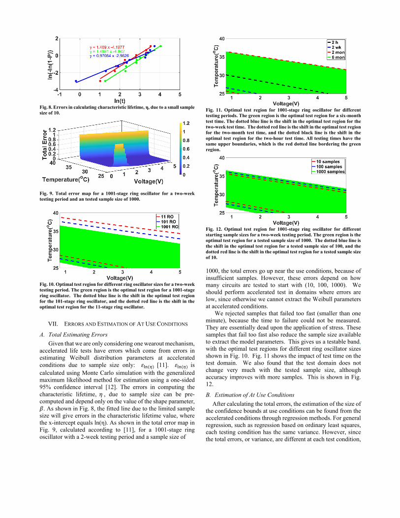
Fig. 8. Errors in calculating characteristic lifetime, η, due to a small sample size of 10.
Fig. 9. Total error map for a 1001-stage ring oscillator for a two-week testing period and an tested sample size of 1000.
Fig. 10. Optimal test region for different ring oscillator sizes for a two-week testing period. The green region is the optimal test region for a 1001-stage ring oscillator. The dotted blue line is the shift in the optimal test region for the 101-stage ring oscillator, and the dotted red line is the shift in the optimal test region for the 11-stage ring oscillator.
VII. ERRORS AND ESTIMATION OF AT USE CONDITIONS
A. Total Estimating Errors
Given that we are only considering one wearout mechanism, accelerated life tests have errors which come from errors in estimating Weibull distribution parameters at accelerated conditions due to sample size only: [11]. is calculated using Monte Carlo simulation with the generalized maximum likelihood method for estimation using a one-sided 95% confidence interval [12]. The errors in computing the characteristic lifetime, , due to sample size can be pre-computed and depend only on the value of the shape parameter,
. As shown in Fig. 8, the fitted line due to the limited sample size will give errors in the characteristic lifetime value, where the x-intercept equals ln(η). As shown in the total error map in Fig. 9, calculated according to [11], for a 1001-stage ring oscillator with a 2-week testing period and a sample size of
Fig. 11. Optimal test region for 1001-stage ring oscillator for different testing periods. The green region is the optimal test region for a six-month test time. The dotted blue line is the shift in the optimal test region for the two-week test time. The dotted red line is the shift in the optimal test region for the two-month test time, and the dotted black line is the shift in the optimal test region for the two-hour test time. All testing times have the same upper boundaries, which is the red dotted line bordering the green region.
Fig. 12. Optimal test region for 1001-stage ring oscillator for different starting sample sizes for a two-week testing period. The green region is the optimal test region for a tested sample size of 1000. The dotted blue line is the shift in the optimal test region for a tested sample size of 100, and the dotted red line is the shift in the optimal test region for a tested sample size of 10. 1000, the total errors go up near the use conditions, because of insufficient samples. However, these errors depend on how many circuits are tested to start with (10, 100, 1000). We should perform accelerated test in domains where errors are low, since otherwise we cannot extract the Weibull parameters at accelerated conditions.
We rejected samples that failed too fast (smaller than one minute), because the time to failure could not be measured. They are essentially dead upon the application of stress. These samples that fail too fast also reduce the sample size available to extract the model parameters. This gives us a testable band, with the optimal test regions for different ring oscillator sizes shown in Fig. 10. Fig. 11 shows the impact of test time on the test domain. We also found that the test domain does not change very much with the tested sample size, although accuracy improves with more samples. This is shown in Fig. 12.
B. Estimation of At Use Conditions
After calculating the total errors, the estimation of the size of the confidence bounds at use conditions can be found from the accelerated conditions through regression methods. For general regression, such as regression based on ordinary least squares, each testing condition has the same variance. However, since the total errors, or variance, are different at each test condition,
ordinary least squares regression cannot be used; weighted regression, also known as weighted least squares, is used to find the lifetime and confidence bounds instead. In weighted regression, the deviation between the observed and expected values of yi is multiplied by a weight wi chosen inversely proportional to the variance at that testing condition for n samples, :
1 (6)
where i=1, …b are the test points, and
(7)
and then solving
(8)
where W is a diagonal matrix of elements and are the regression coefficients. The linear regression equation for FEOL TDDB can be approximated as:
ln ln . (9)
We now consider the problem of selecting the test conditions. The goal is to determine the test condition to minimize the projected confidence interval at use conditions by minimizing:
(10)
where are at use conditions and 1 (residual mean squares follow a normal distribution).
We minimize this variance to find the optimal testing conditions. In prior work we have considered a wide variety of test plans [13]. We found that for all acceleration test domains, either two- or three-point test plans with duplicates minimize errors at use conditions. We have considered all possible two- and three-point test plans and found that the two-point test plans were best for the ring oscillators. Therefore, two test points with duplicates of (VL, T0) and (VH, T0) were used to find the minimum total variance as [14]:
ln lnln lnln ln
ln ln
(11)
where VL is the higher value of the accelerated voltage, VH is the lower value of the accelerated voltage, 0.8 is the at use condition, and 25 is the at use condition. and are the variance due to n samples at each of the test points.
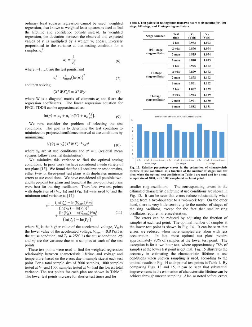
These test points were used to find the weighted regression relationship between characteristic lifetime and voltage and temperature, based on the errors due to sample size at each test point. For a total sample size of 2000 samples, 1000 samples tested at VL and 1000 samples tested at VH had the lowest total variance. The test points for each plan are shown in Table I. The lower test points increase for shorter test times and for
Table I. Test points for testing times from two hours to six months for 1001-stage, 101-stage, and 11-stage ring oscillators.
Stage Number Test time
VL (Volt)
VH (Volt)
1001-stage ring oscillator
2 hrs 0.952 1.073
2 wks 0.876 1.074
2 mon 0.855 1.074
6 mon 0.840 1.075
101-stage ring oscillator
2 hrs 0.975 1.102
2 wks 0.899 1.102
2 mon 0.878 1.102
6 mon 0.861 1.102
11-stage ring oscillator
2 hrs 1.002 1.129
2 wks 0.923 1.129
2 mon 0.901 1.130
6 mon 0.882 1.131
Fig. 13. Relative percentage errors in the estimation of characteristic lifetime at use conditions as a function of the number of stages and test time, when the optimal test conditions in Table 1 are used and for a total sample size of 2000, with 1000 samples at each test point. smaller ring oscillators. The corresponding errors in the estimated characteristic lifetime at use conditions are shown in Fig. 13. It can be seen that errors reduce substantially when going from a two-hour test to a two-week test. On the other hand, there is very little sensitivity to the number of stages of the ring oscillator, except for the fact that smaller ring oscillators require more acceleration.
The errors can be reduced by adjusting the fraction of samples at each test point. The optimal number of samples at the lower test point is shown in Fig. 14. It can be seen that errors are reduced when more samples are taken with less acceleration. In fact, most optimal test plans require approximately 90% of samples at the lower test point. The exception is for a two-hour test, where approximately 78% of samples at the lower test point is optimal. Fig. 15 illustrates the accuracy in estimating the characteristic lifetime at use conditions when uneven sampling is used, according to the optimal results in Fig. 14 and optimal test points in Table 1. By comparing Figs. 13 and 15, it can be seen that substantial improvements in the estimation of characteristic lifetime can be achieve through uneven sampling. Also, as noted before, errors

Fig. 14. Fraction of samples at the lower test point in Table 1, assuming a total sample size of 2000, which minimizes the error in estimating the characteristic lifetime at use conditions, as a function of the number of stages and test time.
Fig. 15. Relative percentage errors in the estimation of characteristic lifetime at use conditions as a function of the number of stages and test time, when the optimal test conditions in Table 1 are used in combination with unequal sampling (illustrated in Fig. 14) and for a total available sample size of 2000. are substantially reduced when increasing the test time from two hours to two weeks. However, improvements from going from two weeks to six months are small. Errors are slightly reduced when using larger ring oscillators.
VIII. CONCLUSIONS
The parameters for choosing the test conditions for accelerated testing were explored by looking at testing time, sample size, and the number of stages for a ring oscillator. The failure probability increases as the testing time is increased, and the characteristic lifetime decreases as the testing time is increased. The sample size for a 95% confidence level for detecting at least one failure can change by one order of magnitude as the testing time is increased from two hours to two weeks, and also from two weeks to two months. As the number of stages is increased, fewer samples are required to detect failures, and the testing time can be lowered. The optimal testing conditions were computed by minimizing error. It was found that errors are reduced substantially when going from a two-hour test to two weeks, and by using an optimal number of samples at each test condition.
ACKNOWLEDGMENTS
The authors would like to gratefully acknowledge Dr. Yi-Da Wu and Li-Hsiang Lin for their helpful discussions. The authors would like to thank the NSF for support under Award Number 1700914.
REFERENCES
[1] J. McLeish, "Physics of Failure Based Simulated Aided/Guided Accelerated Life Testing," in Ann. Reliability and Maintainability Symp. (RAMS), 2018.
[2] G. Huairui and P. Rong, "D-optimal reliability test design for two-stress accelerated life tests," in IEEE Int. Conf. on Industrial Engineering & Engineering Management, 2007, pp. 1236-1240.
[3] S. Hsu, K. Yang, and L. Milor, "Machine Learning for Detection of Competing Wearout Mechanisms," in IEEE Int. Reliability Physics Symp. (IRPS), 2019.
[4] E. Wu, J. Suñé, W. Lai, E. Nowak, J. McKenna, A. Vayshenker, and D. Harmon, "Interplay of voltage and temperature acceleration of oxide breakdown for ultra-thin gate oxides," Solid-State Electronics, vol. 46, pp. 1787-1798, 2002.
[5] C. Chen and L. Milor, "Microprocessor Aging Analysis and Reliability Modeling Due to Back-End Wearout Mechanisms," IEEE Trans. on Very Large Scale Integration (VLSI) Systems, vol. 23, pp. 2065-2076, 2015.
[6] T. Liu, C. Chen, and L. Milor, "Comprehensive Reliability-Aware Statistical Timing Analysis Using a Unified Gate-Delay Model for Microprocessors," IEEE Trans. on Emerging Topics in Computing, vol. 6, pp. 219-232, 2018.
[7] K. Yang, T. Liu, R. Zhang, and L. Milor, "A Comprehensive Time-Dependent Dielectric Breakdown Lifetime Simulator for Both Traditional CMOS and FinFET Technology," IEEE Trans. on Very Large Scale Integration (VLSI) Systems, vol. 26, pp. 2470-2482, 2018.
[8] M. Bashir, D. H. Kim, K. Athikulwongse, S. K. Lim, and L. Milor, "Backend low-k TDDB chip reliability simulator," in Int. Reliability Physics Symp., 2011, pp. 2C.2.1-2C.2.10.
[9] M. Bashir and L. Milor, "Towards a chip level reliability simulator for copper/low-k backend processes," in Design, Automation & Test in Europe Conference & Exhibition (DATE), 2010, pp. 279-282.
[10] M. Bashir, L. Milor, D. H. Kim, and S. K. Lim, "Methodology to determine the impact of linewidth variation on chip scale copper/low-k backend dielectric breakdown," Microelectronics Reliability, vol. 50, pp. 1341-1346, 2010.
[11] K. Yang, R. Zhang, T. Liu, D. Kim, and L. Milor, "Optimal Accelerated Test Regions for Time- Dependent Dielectric Breakdown Lifetime Parameters Estimation in FinFET Technology," in Conf. on Design of Circuits and Integrated Systems (DCIS), 2018.
[12] J. Jacquelin, "Inference of sampling on Weibull parameter estimation," IEEE Trans. on Dielectrics and Electrical Insulation, vol. 3, pp. 809-816, 1996.
[13] D. Kim, S. Hsu, and L. Milor, "Optimization of Experimental Designs for System-Level Accelerated Life Test in a Memory System Degraded by Time-Dependent Dielectric Breakdown," IEEE Trans. on Very Large Scale Integration (VLSI) Systems, vol. 27, no. 7, pp. 1640-1651, 2019.
[14] K. Yang, R. Zhang, T. Liu, S.-H. Hsu, D.-H. Kim, and L. Milor, “Optimal Accelerated Test Framework for Time-Dependent Dielectric Breakdown Lifetime Parameters Estimation,” submitted to IEEE Trans. on Very Large Scale Integraiton (VLSI) Systems.
Copyright © 2022 FDOKUMEN