Recent progress in voltage control of magnetism - arXiv
181
1 Recent progress in voltage control of magnetism: Materials, mechanisms, and performance Cheng Song, a,b,* Bin Cui, a,† Fan Li, a,b Xiangjun Zhou, a Feng Pan a,b a Key Laboratory of Advanced Materials (MOE), School of Materials Science and Engineering, Tsinghua University, Beijing 100084, China. b Beijing Innovation Center for Future Chip, Tsinghua University, Beijing 100084, China. Abstract Voltage control of magnetism (VCM) is attracting increasing interest and exciting significant research activity driven by its profound physics and enormous potential for application. This review article aims to provide a comprehensive review of recent progress in VCM in different thin films. We first present a brief summary of the modulation of magnetism by electric fields and describe its discovery, development, classification, mechanism, and potential applications. In the second part, we focus on the classification of VCM from the viewpoint of materials, where both the magnetic medium and dielectric gating materials, and their influences on magnetic modulation efficiency are systematically described. In the third part, the nature of VCM is discussed in detail, including the conventional mechanisms of charge, strain, and exchange coupling at the interfaces of heterostructures, as well as the emergent models of orbital reconstruction and electrochemical effect. The fourth part mainly illustrates the typical performance characteristics of VCM, and discusses, in particular, * Corresponding author. Tel: +86-10-62781275; fax: +86-10-62771160 E-mail address: [email protected] † Present at Max-Planck Institute of Microstructure Physics, Weinberg 2, D-06120 Halle, Germany
-
Upload
khangminh22 -
Category
Documents
-
view
0 -
download
0
Transcript of Recent progress in voltage control of magnetism - arXiv

1
Recent progress in voltage control of magnetism: Materials,
mechanisms, and performance
Cheng Song,a,b,*
Bin Cui,a,†
Fan Li,a,b
Xiangjun Zhou,a Feng Pan
a,b
a Key Laboratory of Advanced Materials (MOE), School of Materials Science and
Engineering, Tsinghua University, Beijing 100084, China.
b Beijing Innovation Center for Future Chip, Tsinghua University, Beijing 100084,
China.
Abstract
Voltage control of magnetism (VCM) is attracting increasing interest and exciting
significant research activity driven by its profound physics and enormous potential for
application. This review article aims to provide a comprehensive review of recent
progress in VCM in different thin films. We first present a brief summary of the
modulation of magnetism by electric fields and describe its discovery, development,
classification, mechanism, and potential applications. In the second part, we focus on
the classification of VCM from the viewpoint of materials, where both the magnetic
medium and dielectric gating materials, and their influences on magnetic modulation
efficiency are systematically described. In the third part, the nature of VCM is
discussed in detail, including the conventional mechanisms of charge, strain, and
exchange coupling at the interfaces of heterostructures, as well as the emergent
models of orbital reconstruction and electrochemical effect. The fourth part mainly
illustrates the typical performance characteristics of VCM, and discusses, in particular,
* Corresponding author. Tel: +86-10-62781275; fax: +86-10-62771160
E-mail address: [email protected] † Present at Max-Planck Institute of Microstructure Physics, Weinberg 2, D-06120
Halle, Germany

2
its promising application for reducing power consumption and realizing high-density
memory in several device configurations. The present review concludes with a
discussion of the challenges and future prospects of VCM, which will inspire more
in-depth research and advance the practical applications of this field.
Keywords: Voltage control of magnetism; Electrical control of magnetism;
Magnetoelectric coupling; MRAM; Spintronics
Abbreviations:
2-DEG two dimensional electron gas; AAIM, 1,3-diallylimidazolium; ABIM,
1-allyl-3-butylimidazolium; AEIM, 1-al-lyl-3-ethylimidazolium; AFM,
antiferromagnetic; AHE, anomalous Hall effect; ALD, atomic layer deposition; α,
magnetoelectric coupling coefficient; BFO, BiFeO3; BTO, BaTiO3; CFO, CoFe2O4;
DEME, N,N-diethyl-N-(2-methoxyethyl)- N-methylammonium; DOS, densities of
states; EDL, electric double layer; EELS, electron energy loss spectroscopy; EMIM,
1-ethyl-3-methylimidazolium; FE, ferroelectric; FE-FET, ferroelectric field effect
transistor; FET, field-effect transistor; FM, ferromagnetic; GMR, giant
magnetoresistance; HAADF, high angle annular dark field; HM, heavy metal; HC,
coercive field; HEB, exchange bias field; IL, ionic liquid; κ, dielectric constant or
permittivity; KU, magnetocrystalline anisotropy; LAO, LaAlO3; LCMO,
La1–xCaxMnO3; LSMO, La1–xSrxMnO3; λ, screening length; MA, magnetic anisotropy;
MAE, magnetocrystalline anisotropy; MFM, magnetic force microscopy; MFTJs,
multiferroic tunnel junctions; MOKE, magneto-optic Kerr effect; MPPR,
N-methyl-N-propylpiperidinium; MR, magnetoresistance; MRAMs, magnetic random
access memories; MTJ, magnetic tunnel junction; m, magnetic moment; MS, saturated

3
magnetization; NFO, NiFe2O4; PCMO, Pr1–xCaxMnO3; PEEM, photoemission
electron microscopy; PEO, polyethylene oxide; PLD, pulsed laser deposition; PMA,
perpendicular magnetic anisotropy; PMN-PT, PbMg1/3Nb2/3)O3-PbTiO3; PTO, PbTiO3;
PZT, PbZr1–xTix)O3; P, polarization; Pdown, polarization downward; Pup, polarization
upward; Φ, potential barrier; RHall, Hall resistance; SHE, spin Hall effect; SOT,
spin–orbit torque; SQUID, superconducting quantum interference device; SRO,
SrRuO3; STEM, scanning transmission electron microscopy; STO, SrTiO3;
STT-MRAM, spin transfer torque magnetic random access memory; σ, spin
polarization direction; TER, tunnel electroresistance; TFSI,
bis-(trifluoromethylsulfonyl)imide); TMPA, N,N,N-trimethyl-N-propylammonium;
TMR, tunnel magnetoresistance; T, temperature; TC, Curie temperature; τDL,
damping-like torque; τFL, field-like torque; VCM, voltage control of magnetism;
VCMA, voltage control of magnetic anisotropy; VG, gate voltage; VO, oxygen
vacancies; XANES, x-ray absorption near edge structure; XAS, x-ray absorption
spectroscopy; XLD, x-ray linear dichroism; XMCD, x-ray magnetic circular
dichroism; YIG, Y3Fe5O12; YMO, YMnO3;
Contents
1. Introduction
2. Film materials for voltage control of magnetism
2.1 Magnetic medium
2.1.1 Magnetic metals
2.1.2 Magnetic semiconductors
2.1.3 Magnetic oxides
2.2 Dielectric gating medium

4
2.2.1 Normal dielectric and high κ materials
2.2.2 Ferroelectric crystals and films
2.2.3 Electrolytes
3. Mechanisms under voltage control of magnetism
3.1 Carrier modulation
3.1.1 Modulation of carrier density in ultrathin metals
3.1.2 Modulation of carrier density in diluted magnetic semiconductors
3.1.3 Modulation of carrier density in ferromagnetic oxides
3.1.4 Modulation of carrier density in non-magnetic oxide heterostructures
3.2 Strain effect
3.2.1 Strain mediation in ferromagnetic metal/ferroelectric oxide bilayers
3.2.2 Strain mediation of antiferromagnetic metals
3.2.3 Strain mediation in ferromagnetic/ferroelectric oxide heterostructures
3.3 Exchange coupling
3.3.1 Voltage control of exchange coupling in multiferroic heterostructures
3.3.2 Voltage control of exchange springs in antiferromagnetic alloys
3.4 Orbital reconstruction
3.4.1 Electrically induced orbital reconstruction in ferromagnetic metals
3.4.2 Electrically induced orbital reconstruction in ferromagnetic oxides
3.5 Electrochemical effect
3.5.1 Interfacial oxidation of metals under electric fields
3.5.2 Magnetic phase transition of oxides under electric fields
3.6 Comparison of five different mechanisms
4. Applications of voltage control of magnetism in spintronics
4.1 Electric field-assisted switching in tunneling junction
5
4.1.1 Significant decrease in energy consumption
4.1.2 Promise for high-density storage via four-state memory
4.2 Electric field-driven magnetization reversal
4.2.1 Magnetization switching assisted by a small magnetic field
4.2.2 Magnetization switching realized under no magnetic field
4.3 Electric field modulation combined with current in spintronics
4.3.1 Spin–orbit torque
4.3.2 Electric field control of spin–orbit torque
5. Conclusion and Outlook
Acknowledgements
References
1. Introduction
The control of magnetism and spin phenomena, which corresponds to switching
between the basic “0” and “1” signals in information technology, has been intensely
pursued during the past few decades [1–4]. It has generally been accepted that a
magnetic field is the only means to switch magnetization and to maintain unchanged
the magnetic behaviors of magnetic materials once they have been prepared [4]. The
use of cumbersome magnets or coils occupies a large amount of space and entails
serious energy consumption, especially when taking the remarkable trend in
miniaturization of magneto-electronics into account [4–6]. Thus, there is a pressing
need to employ nonmagnetic means to switch and modulate magnetism. Compared
with other nonmagnetic routes, such as strain, doping, current, and light, etc., a
voltage has been proven to be able to manipulate magnetism with a combination of
advantages, including low power dissipation, reversibility, nonvolatility, high speed,

6
and good compatibility with the conventional semiconductor industry [7–13].
In fact, Maxwell’s equations first reveal that the two independent phenomena of
magnetic interaction and electric charge motion are intrinsically coupled to each other
[14]. The thought of utilizing electric fields to control magnetism could date back to
the 1960s [15]. In 2000, Ohno et al. [16] demonstrated the tuning of saturated
magnetization and Curie temperature by an electric field in a diluted magnetic
semiconductor (In,Mn)As. A large number of experimental works and theoretical
investigations on the modulation and switching of magnetism have emerged in recent
years, driven both by an urge to understand the mechanisms involved and by the
demand for better performance, which is shown by the increasing number of
publications every year as depicted in Fig. 1. The research regarding the interaction
between charge and spin has developed into the exciting area of voltage control of
magnetism (VCM). This field shows great potential to impact magnetic data storage,
spintronics, and high-frequency magnetic devices, especially taking into account
recent initiatives in internet of things, big data, artificial intelligence, and cloud
computing.
Inspired by studies on magnetic semiconductors, researchers began investigating
the voltage control of magnetic metals. Although it was previously thought that is was
difficult to realize a large enough electric field effect in metals due to the short
screening length [17], the manipulation of magnetism with an electric field effect was
observed in ultrathin FePt and FePd owing to the large electric field-induced
modulation of surface charges through ionic liquid gating [18]. Relevant
investigations were soon expanded to ferromagnetic metal/ferroelectric oxide bilayers,
such as Ni/BTO and CoFe/BFO, as well as Ta/CoFeB/MgO sandwiches [19–21]. The
latter are the fundamental heterostructures for the current read–heads in high-density

7
hard disks and the emerging magnetic random access memory (MRAM) technologies
[3]. Since ultrathin metals are commonly used for electrical modulation, the interface
of ferromagnetic metal/dielectric gating profoundly affects the efficiency of VCM.
Thus the role of the interface in the VCM was extensively discussed in previous
publications [22–24].
On the other hand, complex oxides have drawn increasing attention in recent years,
because the strong couplings between lattice, charge, spin, and orbital degrees of
freedom provide a broad playground for a variety of exotic properties tuned by
various electrical methods including VCM [25]. Thanks to the high permittivity (κ)
and the low carrier density (n), oxide thin films often display a much larger screening
length (tS = (κħ2/4me
2)1/2
(1/n)1/6
, ħ is the Planck constant, m and e are the electron
mass and charge, respectively), guaranteeing a strong electric field effect for the
manipulation of magnetic properties. The typical examples of VCM are found in
multiferroic-based oxide bilayers, such as LSMO/PMN-PT, PZT/LSMO and
LSMO/BFO [26–28]. These systems were commonly involved in inverse
magnetoelectric coupling [29,30], a revival in multiferroic materials from the 1980s.
That is, changing the magnetic properties (ΔM) by applying an external electric field
(ΔE), ΔM = αΔE, where α is magnetoelectric coupling coefficient [30]. It is worth
pointing out that inverse magnetoelectric coupling could be considered a typical VCM
behavior to some extent when ferromagnetic/ferroelectric bilayer films are used. In
recent years, the magnetic properties of ferromagnetic films, including saturated
magnetization (MS), coercive field (HC), magnetic anisotropy (MA), and Curie
temperature (TC), etc., have been effectively manipulated by electrical means
[24,31,32].
In terms of the mechanisms embedded in VCM, there are various origins. First,

8
the modification of charge carrier densities is thought to play a crucial role in
ferromagnetic semiconductors and oxides [33,34]. An induced or spontaneous electric
polarization at the interface of the dielectric/magnetic layers results in carrier
accumulation or depletion, leading to a variation in the magnetic exchange interaction
and anisotropy. In magnetic metals, the electric field manipulates the carrier density
and the resultant Fermi level position at the interface, which determines the magnetic
anisotropy [24,35]. The progress in ferromagnetic/ferroelectric heterostructures has
brought about significant innovation in the mechanisms for VCM, where the strain
effect is commonly involved. As known as the inverse piezoelectric effect, an external
electric field would change the lattice of ferroelectric crystals when the ferroelectric
switching occurs. The strain induced by the lattice variation is then transferred to the
adjacent magnetic layer, causing modulations of magnetic properties through
magnetostriction [36]. Once the ferroelectric layer is replaced by a multiferroic film
(e.g., BFO) with a combination of ferroelectric and antiferromagnetic features, the
exchange coupling mechanism provides another route for the electrical modulation of
the spin arrangement in the ferromagnetic layer [37,38].
The textbook-style mechanisms referring to charge, lattice, and spin degrees of
freedom mentioned above have been widely summarized in previous reviews
[30,31,39,40]. Interestingly, recent advances in the characterizations of cutting-edge
electronic structures and in dielectric materials indicate that two emergent
mechanisms, orbital reconstruction and the electrochemical effect, are responsible for
VCM in some systems. For example, the interfacial modulation of Mn orbital
occupancy in LSMO/BTO heterostructures alters the TC and magnetoresistance of
LSMO [41]. The situation turns out to be dramatically different when the inert oxide
gate is replaced by an ionic conductor (e.g., GdOx) with high O2−
mobility or an

9
electrolyte; the ion motion and the subsequent reversible redox in the magnetic
medium driven by a gate voltage leads to a variation of magnetic anisotropy and
saturated magnetization [42,43].
More than one and a half decades have already passed since the first experimental
report on VCM in (In,Mn)As. The focus is gradually shifting not only toward the
excavation of in-depth physical mechanisms, but also toward the improvement of
application-oriented performance. One of the most promising examples of nonvolatile
memory, spin-transfer torque magnetic random access memory (STT-MRAM) is at
the heart of information storage and spintronic devices [6,10]. The present
STT-MRAM chips with the storage volume of 64 Mb have shown extensive
applications, including aerospace industry and automobile industry. Very recently,
Everspin began planning production of 256 Mb and 1 Gb products [44], and SK
Hynix and Toshiba also announced 4 Gb STT-MRAM in 2016 International Electron
Devices Meeting [45]. Such a scale of storage volume is comparable to that of DRAM
(dynamic random access memory), and even higher than that of SRAM (static random
access memory). These achievements promote this promising memory design to the
multi-billion dollar market for persistent memory in the field of storage devices and
servers, which could be used in the internet of things, big data, artificial intelligence,
and cloud computing, etc. Nevertheless, to realize magnetization switching by
spin–transfer torque (STT), a high current density (106 A/cm
2) passing through each
magnetic tunnel junction is persistently needed [6]. As it is generally accepted that the
threshold current of semiconductors is at 105 A/cm
2, the operation of magnetization
switching in MRAM with a lower density current is particularly urgent. It is
considered to be fundamentally transformative once an external voltage can assist or
achieve magnetization switching. This interesting phenomenon was observed in

10
CoFeB/MgO/CoFeB junctions, where the magnetization behaviors and tunneling
magnetoresistance were manipulated by voltage pulses associated with much smaller
current densities of 104 A/cm
2 [46], and even a low switching energy of ~6 fJ/bit
[47,48]. In this scenario, voltage-controlled magnetic anisotropy (VCMA) coefficient
is employed to evaluate the energy efficient writing [49,50]. Moreover, the
multiferroic tunnel junction with the ferromagnetic and ferroelectric orders exhibits
four distinct resistance states with a combination of electric and magnetic fields,
which provides a promising way toward the realization of high-density memory.
On the other hand, the use of pure voltage to realize deterministic nonvolatile 180º
magnetization switching is highly sought after, not only driven by an understanding of
fundamental physics, but also motivated by an eagerness for information storage with
low power consumption. To replace the magnetic field with an electric field in a
magnetization reversal, the electric field-controlled exchange coupling and
interactions between the ferroelectric–ferromagnetic domains are utilized in
CoFe/BFO [51] and CoFeB/IrMn/PMN-PT [52]. Note that spin–orbit torque (SOT)
provides an alternative way to achieve current-induced magnetization switching
through a public line. A three-layer structure consisting of heavy metal/ferromagnetic
metal/oxide is conventional in the study of SOT, where the spin Hall effect from
heavy metals (such as Pt and Ta) and/or the Rashba effect from the inversion
asymmetry of the interfaces contribute to the spin–orbit torque and the effective
switching field [53–55]. Recently, the control of SOT in both metallic heterostructures
and topological insulators was reported with the purpose of decreasing the critical
switching current, which is an extension of VCM [56–58].
Although large amount of significant works have been done in the area of VCM, it
is still a developing and energetic research topic with a lot of open questions in the

11
performances, fundamental mechanisms, and practical applications of VCM. Firstly,
the magnetic medium, dielectric gating, and their interface profoundly affect VCM
with different behaviors and efficiencies. Note that the type of dielectric gating not
only affects the manipulation efficiency, but also determines the intrinsic features of
electrical modulation [59–62]. Even more ambiguously, opposite modulation
tendencies are commonly observed in very analogical ferromagnetic metal systems.
For instance, it is reported that positive gate voltage enhances the perpendicular
magnetic anisotropy [22,24], whereas it does the opposite in other works [23]. Thus,
there is a pressing need to sort out electrical modulation at the category level to
address the question of how the magnetic medium and dielectric gating affect VCM.
Secondly, the mechanisms responsible for magnetization modulation by electric fields
are hard to separate completely in experiments [32,63]. For example, the carrier
density modulation and strain effect are commonly mixed together in
ferromagnetic/ferroelectric bilayers, because the ferroelectric polarization always
causes both charge accumulation/depletion and a simultaneous strain effect [64,65].
Moreover, from the perspective of fundamental research, further development of
VCM relies heavily on a thorough elucidation of the underlying mechanism, which
has provoked studies for several novel mechanisms in brand new systems during the
last few years. Thirdly, VCM is proposed to establish the next generation nonvolatile
memory technologies with ultralow power consumption, high density, high speed, and
a good compatibility with the semiconductor industry. To switch the magnetization or
reduce the current density in current-induced magnetization reversal by external
voltage are promising ways for the further reducing of the power consumption in
spintronic devices.
Our review aims to supply a comprehensive summary of the burgeoning field of

12
VCM and illuminate its distinct mechanisms. After this brief introduction in Section 1,
we will illustrate the materials for the magnetic medium and dielectric gating, as well
as various properties manipulated by the electric field in Section 2. Considering that
the three conventional mechanisms cannot satisfy the rapid development of VCM in
different novel systems, the latest mechanisms are added and discussed in Section 3.
Subsequently, in Section 4 we discuss the recent focus on the promising application of
VCM in spintronics. Finally, the challenges and future prospects for voltage control of
magnetism are presented. It should be clarified that it is an almost impossible mission
to depict all the studies carried out worldwide due to the fast pace of research in this
area, and therefore some publications will inevitably be missed.
2. Film materials for voltage control of magnetism
Materials used for voltage control of magnetism can be classified into magnetic
and dielectric materials according to their roles. An electric field forms via the
dielectric materials under an applied external voltage and, subsequently, the
performance of the magnetic materials is modulated under the electric field. To
combine these two materials together for VCM, four types of device configurations
are generally adopted as shown in Fig. 2: FET (field effect transistor) type, where the
dielectric layer lays on the magnetic layer; BG (back gating) type, where the dielectric
layer lays beneath the magnetic layer as a back grid; MTJ (magnetic tunnel junction)
type, where the dielectric layer is sandwiched by two magnetic layers as a barrier);
and, the Nano (nanostructure) type, where dielectric and magnetic materials are
grouped together in the form of a nanostructure. FET-type VCM devices are
developed from traditional FETs in the semiconductor industry, which usually utilize
electric field-induced carrier density variation to manipulate the magnetic properties
13
in semiconductor, oxides, and ultrathin ferromagnetic metal. In BG-type devices,
piezoelectric materials or multiferroic materials, e.g. PMN-PT or BFO, are generally
used as the bottom grid to control the magnetic metals and oxides through strain
transfer or exchange coupling. In the MTJ-type devices, it is convenient to manipulate
the magnitude and even a sign of magnetoresistance via the external voltage. In
contrast, nano-type devices are based on some ferromagnetic-ferroelectric oxides
systems, which can form self-assembled or artificial nanostructures, demonstrating a
remarkable VCM due to the enhanced magnetoelectric coupling.
Note that magnetic metals dominate in the information storage devices, both in
hard disk and the emerging MRAM. Since VCM was first realized in diluted magnetic
semiconductors, taking advantage of the electric field effect on magnetism-related
carrier density, magnetic materials have been extended from initial semiconductors to
metals and then oxides, associated with a deeper insight and an extended
understanding of the underlying mechanisms. At the same time, with the increased
demand for a larger electric field effect, many efforts have been made to replace the
traditional normal dielectric materials with either ferroelectric materials with a
spontaneous polarization or electrolytes with an electric double layer to enhance the
effect. As the materials vary, the mechanism underlying the VCM differs, involving
five distinct embedded mechanisms: i) modulation of charge carrier densities (Charge),
ii) strain effect (Strain), iii) exchange coupling or exchange bias (EB), iv) orbital
reconstruction (Orbital), and v) electrochemical redox (Electrochemistry). In
consequence, we mainly focus on the character of magnetic materials and dielectric
materials in this section, accompanied by a brief introduction of the corresponding
mechanisms in some comprehensive tables, which can help in the selection and design
for VCM.

14
2.1 Magnetic medium
Almost all magnetic materials have the potential to be controlled by electric fields.
For example, macroscopic magnetic properties of ferromagnetic films, including MA,
HC, MS, exchange bias field (HEB), TC, and magnetoresistance (MR) have been
effectively manipulated by electrical means, as shown in Fig. 3. In addition, domain
wall movement under an external magnetic field can be manipulated by voltages as
well. According to the conductive character and chemical composition, magnetic
materials can be classified into magnetic metals, semiconductors, and oxides.
Magnetic metals, which have a wide application in the information technology
industry, show the advantages of strong magnetization, high TC, simple fabrication,
low cost, and possible perpendicular magnetic anisotropy (PMA) [1,2]. Nevertheless,
the short screening length in metals due to the high conductivity seriously limits the
VCM [24,66]. Compared with metals, semiconductors show a remarkable superiority
in large screening length, but an inferior one in small magnetic moments and low TC
[2,67], while oxides exhibit high thermostability and abundant physical properties
[25,31,68], which would supply more opportunities for voltage control.
2.1.1 Magnetic metals
Taking advantage of the superiority of robust magnetization, high TC, and possible
PMA, many attempts have been made in magnetic metals to achieve VCM
experimentally and theoretically, involving magnetic metals or alloys such as Fe, Co,
Ni, Co/Ni, Co/Pd, Fe-Ga, FePt, FePd, CoFe, CoPd, NiFe, and CoFeB. The robust
magnetization and high TC guarantee the performance at room temperature while the
properties of PMA show great application potential in the information technology
industry. Although the short screening length due to the high conductivity of metals

15
limits the electric field effect, a breakthrough was achieved via enhancement of the
electric field with the introduction of ferroelectric (FE) materials and electrolytes as
the dielectric materials. At the same time, an effective control of magnetism by
external voltages has been observed recently in some AFM metals (e.g., IrMn and
FeMn) and metals with an FM–AFM transition (e.g., FeRh), which enriches the
metallic system for VCM [69–71]. To summarize this research in magnetic metals, the
device structure, magnetoelectric coupling coefficient (α), temperature (T), coupling
mechanism, and corresponding results of voltage control are listed in Table 1.
Achieving an effective control of magnetism in metals via the electric field is
mainly realized through three device types, that is, FET-type, BG-type, and MTJ-type
devices. The FET type with the dielectric layer laid above the magnetic layer and the
BG type with the dielectric layer embedded under the magnetic layer are commonly
used in designs to attain a large electric field via the electrolyte and ferroelectric
layers, respectively. At the same time, the MTJ type with a
current-perpendicular-to-plane structure (the current is perpendicular to the plane) is
often considered in topics on VCM as well, which show an exclusive potential for
high-density storage.
In FET-type devices with the dielectric layer on the surface, a large electric field
can be easily applied on the magnetic layer with the help of an electrolyte
(particularly an ionic liquid). Thus, through many attempts, various performance
behaviors of magnetic metals have been successfully modulated by electric fields,
with the breakthrough in the short screening length limitation. By immersing the
device in an electrolyte, magnetocrystalline anisotropy and coercivity in ultrathin FePt
and FePd of 2 nm is modulated by an electric field [18]. With the gate voltage applied
through an ionic liquid (IL), voltage control of FM metals was observed in similar

16
structures with MgO/Co/Pt [61], HfO2/FeMn/Co/Pt/[Co/Pt]4 [69],
HfO2/IrMn/Co/Pt/[Co/Pt]4 [70], HfO2/Ni/Co/Pt [22], and HfO2/[Co/Ni]n/Pt [62]
heterostructures with PMA, where the magnetic properties were modified, including
magnetic moments, TC, coercivity, magnetic anisotropy, and exchange bias. In
addition, an electric field could also be directly applied on the oxide-capping layer to
gain an effective manipulation of the magnetism. For example, magnetic anisotropy in
MgO/Fe systems is controlled through spin–orbit interaction, where the hybridization
of Fe 3d orbitals and O 2p orbitals or the Fermi surface can be modulated under the
electric field [23,72], while in MgO/FeCo and GdOx/Co, the magnetization, coercivity,
magnetic anisotropy, and domain are modulated under the electric field, due to the
change in the oxidation states of the interfacial magnetic metals [42,43,73,74].
In contrast to the FET structure, in BG-type devices, the dielectric layer is
embedded under the magnetic layer, where FE or piezoelectric materials usually serve
as the dielectric layer to provide an electric field, with the magnetic metal as a top
electrode. Voltage control of magnetism in BG-type devices was first realized in
CoPd/PZT, demonstrating a dependence of the polar Kerr rotation on the external
electric field [75]. After that, the voltage control of magnetic anisotropy (VCMA) and
moment was achieved in many works based on FM/FE heterostructures, e.g., Fe/BTO,
Co/PMN-PT, Ni/BTO, and CoFeB/PMN-PT [19,59,76,77]. With the advances in
characterization methods, the reversible switching of the magnetic domain in
FeGa/BTO using a static (DC) electric field was directly observed by in-situ Lorentz
microscopy [78], while the electrical modulation of domain behavior, that is,
out-of-plane magnetization, was demonstrated in Ni/BTO by XMCD and PEEM [79].
Recently, research interests have tended toward magnetization switching by external
voltages, which have been realized in the heterostructure of Co/PMN-PT and

17
CoFeB/AlOx/CoFeB/PMN-PT MTJ [59,80]. In addition, exchange bias can also be
tuned by voltage with an AFM layer introduced into the heterostructure,
CoFe/BFO/SRO/PMN-PT, CoFe/BFO, [Co/Pt]/Cr2O3, [Co/Pd]/Cr2O3, and
NiFe/YMnO3 [20,60,81–85], etc. Besides FM metals, VCM has been attained in an
FeRh alloy with an FM–AFM transition near room temperature, showing a variation
in transition temperature and giant electroresistance [71,86].
Since the two device types mentioned above are generally in a current-in-plane
configuration, VCM realized in a current-perpendicular-to-plane MTJ-type device has
received much attention for high-density storage applications. In the MTJ-type device,
the MTJ part serves as a pseudocapacitor and most attempts have been focused on the
switching of the magnetization by electric fields, which can be classified into two
schemes, that is, changing the coercivity or magnetic anisotropy, respectively. Based
on the first scheme, a magnetization reversal induced by the electric field in the
CoFeB/MgO/CoFeB MTJ has been observed according to the junction resistance
under a small assistant magnetic field, due to the reduced coercivity of CoFeB under
the electric field [46]. On the other hand, taking advantage of the electric field effect
on magnetic anisotropy, magnetization can be reversed by the voltage pulse in a
Fe/MgO/FeCo MTJ, where the magnetic anisotropy and related switching of the FeCo
layer are modulated by the external voltage while the magnetization of the Fe layer is
stable under electrical stimulation [87,88]. Since the electric field pulse temporarily
arranges the easy axis of the free layer in-plane, the magnetization of the free layer
under an external fixed perpendicular magnetic field is switched. It is noteworthy that
with the increasing thickness of the MgO barrier in the MTJ device, the switching
energy of the electrical switching remarkably decreases [47,48]. It promises a
decrease in energy consumption when combined with the magnetization switching
18
induced by the current via the spin-transfer torque (STT), which shows tremendous
potential for compact memory and integrated circuits with lower energy consumption
[89].
To guarantee a fine magnetic metal layer for VCM, the magnetic metals or alloys
are prepared by different methods, such as magnetron sputtering and electron beam
deposition. Magnetron sputtering is a thin film deposition method that is widely used
in the industry with advantages including high efficiency, yield, and low-cost
production [90,91]. It can meet the deposition requirement of most magnetic metals
and alloys. In contrast, electron beam deposition with a high background vacuum and
the largest energy density of 109 W/cm
2, demonstrates a superiority in the deposition
of highly pure metals and binary oxide films [92]. It is noteworthy that with the
advances in sputtering and electron beam deposition technology, preparation of
magnetic metals with PMA has been realized, including a number of ultrathin FM
metal alloys, such as 01L -ordered (Co,Fe)-Pt alloys, Co/(Pd,Pt) or Co/Ni multilayers,
and CoFeB/MgO [10,22,93,94]. The realization of VCM in most of these systems
brings the promise of a bright future for a new generation high-density nonvolatile
information storage and logic devices, where a fine thermostability and a low critical
current are in demand for current-induced magnetization switching.
2.1.2 Magnetic semiconductors
A magnetic semiconductor is prepared by doping a transition-metal element (e.g.,
Mn and Co) into a nonmagnetic semiconductor (e.g., GaAs, InAs, TiO2, and ZnO)
[9,67], which behaves common semiconductor characteristics and magnetic properties
at the same time. When compared with magnetic metals, FM semiconductors have a
larger screening length, guaranteeing a high efficiency in the voltage control of
magnetic layers. It is well known that FM semiconductors show a strong magnetism

19
dependence on the hole concentration, as described by the p-d Zener model [95]. Thus,
an effective manipulation of magnetism can be attained via the extraction and
injection of hole carriers in the FET channel under positive and negative gate voltages,
accompanied by the suppressed and enhanced TC or magnetic moment, respectively.
FM semiconductors used for VCM are summarized in Table 2.
We focus first on (In,Mn)As and (Ga,Mn)As, which are the most well-known FM
semiconductors. Voltage control of the magnetic phase transition in FM
semiconductors was first observed in (In,Mn)As, as reflected by the modulation of an
anomalous Hall effect (AHE) [16]. Subsequently, the TC, magnetic moment,
magnitude, and sign of the AHE coefficient of (Ga,Mn)As were changed by the
electric field in a series of works [96–104]. Nevertheless, the low intrinsic TC
somehow limits the application of (In,Mn)As and (Ga,Mn)As, which also inspired
much research aimed at the improvement of TC in these systems through various
means such as the proximity effect [105].
Due to the limitation of the low intrinsic TC, studies on the influence of the electric
field on magnetic properties have involved numerous magnetic semiconductors, for
example, groups IV, II–VI, III–V, topological insulators, etc. [106–115]. After 2000,
many studies in experiment and in theory revealed that the TC of some p-type FM
wide-bandgap semiconductors, such as ZnO, TiO2, and GaN, could be enhanced to
higher than room temperature [9,95], which further inspired a new wave of research.
Since ferromagnetism in diluted magnetic oxides like Co:ZnO originates from the
defects in the system such as oxygen vacancies (VO) [116], the AHE and magnetic
phase transition of Co:ZnO and Co:TiO2 can be manipulated by gate voltage applied
through SiOx and IL, respectively [109,111]. Additionally, the saturation
magnetization and coercivity field of Zn0.95Co0.05O in the Pt/Zn0.95Co0.05O/Pt is

20
reversibly controlled, taking advantage of the resistive switching under the electric
field [110]. It is noteworthy that, although diluted magnetic oxides are oxides in
chemical composition, we attribute them to FM semiconductors in light of their
semiconductor conductive character.
In order to achieve VCM in semiconductor-based devices, ultrathin films with a
high crystalline quality are usually needed. In general, narrow gap semiconductors,
like (In,Mn)As, (Ga,Mn)As, and topological insulators, are usually prepared by
molecular beam epitaxy, which is well known for an epitaxial growth of ultrathin
films. On the other hand, diluted magnetic oxides with a wide gap, such as Co:ZnO,
are commonly deposited via magnetron sputtering or pulsed laser deposition.
2.1.3 Magnetic oxides
Magnetic oxides, displaying a multitude of new physics and potential applications,
have drawn a great deal of interest in research since the investigation of the half-metal
oxides, which are promising for the realization of the large tunnel magnetoresistance
effect with high stability and multiple functions (e.g., multiferroics). Since magnetic
oxides, especially perovskite oxides, have a good coherence with FE oxides such as
BTO, PZT, and PMN-PT in the crystal structure, which guarantees the preparation of
high-quality epitaxial FM/FE heterostructures, VCM in magnetic oxides is mainly
achieved in the form of the FET, MTJ, and BG types with FE oxides serving as the
dielectric layer [7,117]. In addition, spinel magnetic oxides ferrites can also be used as
the magnetic layer. It is worth mentioning that multiferroic oxides, for example, BFO,
exhibit both antiferromagnetic and ferroelectric properties at the same time, making it
possible for multiferroic oxides to work as the antiferromagnetic and dielectric layer
simultaneously except for the single role of the dielectric layer in FM/FE
heterostructures. The research on VCM in magnetic oxides is summarized with the

21
corresponding data in Table 3.
As a model for magnetic oxides, manganites lie at the heart of this research in
light of the fact that their TC is close to room temperature, for example, 370 K for
LSMO (x = 0.33). Meanwhile manganites have a high spin polarization to 95% and
rich magnetoresistance, for example, tremendous magnetoresistance, anisotropic
magnetoresistance, and planer Hall magnetoresistance [68,118–120]. Among various
manganites, most studies are focused on LSMO, LCMO, and PCMO for the
realization of VCM. Because the origin of the magnetism is the double exchange in
the Mn3+
-O-Mn4+
chain, where the charge transfer calls for an identical magnetic
structure in two Mn ions [117], the variation in the doping level and corresponding
Mn3+
/Mn4+
ratios can be used to modulate the double exchange, which promises an
effective electric-field manipulation of magnetism via the charge mechanism. Taking
LSMO as an example, a series of magnetic phases appears with the variation in the
doping level [121,122], that is, LSMO changes from an insulating phase with
seriously suppressed magnetism to a good ferromagnet and then an antiferromagnet,
as the Sr doping varies from x < 0.16 to x = 0.16–0.5 and then x > 0.5 [8]. For
example, in FET-type PZT/LSMO and BTO/LSMO heterostructures, TC,
magnetization, and magnetic anisotropy are modulated by the electric field based on
the accumulation and deletion of carriers near the interface, which is controllable via
FE polarization switching [27,34,65,123]. Similarly, in multiferroic tunnel junctions
such as Co/PZT/LSMO and LSMO/BTO/LCMO/LSMO, the tunnel barrier height and
the transition between different magnetic phases are manipulated via the variation in
carrier density under the electric field, reflected in the four-state memory under a
combination of magnetic and electric fields [124,125].
In addition, the electronic phase dependence of manganites on the strain provides

22
an alternative for VCM in manganites, with the strain mechanism playing a dominant
role [126]. For some FM manganites like LSMO, the in-plane tensile strain favors the
in-plane orbital occupancy, resulting in the in-plane magnetic easy axis for even
A-type antiferromagnets with oppositely aligned ferromagnetic planes of the {001},
while the compressive strain stabilizes an occupancy of the orbitals out of plane,
inducing the perpendicular easy axis for even C-type antiferromagnets with oppositely
aligned ferromagnetic planes of the {110} [127,128]. In this way, an electrically
induced strain gained by the inverse piezoelectric effect-induced magnetostriction
could be used to alter the strain-related magnetism in BG-type devices [64]; for
example, in LSMO/PMN-PT, the magnetic moment follows the strain modulation in
FE crystals under an external electric field [26,129].
Compared with perovskite manganites, spinel magnetic oxides ferrites, e.g., CFO,
NFO, and Fe3O4 (or Zn0.1Fe2.9O4), usually show a TC much higher than room
temperature and a large resistivity, making them appropriate for various applications
such as information storage, spintronics, and high-frequency chips [37,130]. Similar
to the case of a perovskite heterostructure, the magnetization and magnetic anisotropy
have been effectively controlled under the electric field in the various heterostructures
of ferrimagnetic spinel/FE perovskite oxides, such as CFO/PMN-PT, NFO/PZT,
Fe3O4/CFO/PZT, Fe3O4/PMN-PT, and Zn0.1Fe2.9O4/PMN-PT [131–138]. Besides the
heterostructure devices, ferrimagnetic spinel/FE perovskite oxide composites with
self-assembled or artificial nanostructures (i.e. Nano-type) also attract significant
attention as a unique system for VCM, where the ME coupling is thought to be
relatively larger than that in the heterostructure devices [139,140]. In general,
composite nanostructures could be classified into two groups: (i) a 0–3 structure that
is usually designed with a magnetic nanostructure implanted in a piezoelectric matrix;

23
(ii) a 1–3 structure, such as single-layer self-assembled structures and some artificially
constructed nano-rods embedded in a piezoelectric matrix [141]. Numerous
investigations of FM spinel/FE perovskite systems have been reported with different
combinations between the FE perovskites (BTO, BFO, PTO, and PZT) and the spinel
phases (CFO and NFO) [130,142–145].
Multiferroic oxides, as a special type of magnetic materials, usually demonstrate
an interaction between the antiferromagnetic and ferroelectric properties, promising a
controllable magnetism under an electric field in a single layer instead of the
commonly used FE/FM oxide multilayers. As one of the most well-known
multiferroics, a large number of works have been carried out on BFO, to realize an
effective control of magnetism involving the antiferromagnetic domain and the spin
wave by electric field-induced ferroelectric switching [146–149]. Similarly, voltage
control of the magnetic structure was demonstrated in multiferroic HoMnO3 [150].
Generally, magnetoelectric composites are prepared by either the PLD or sol–gel
method. The PLD assisted by reflection high-energy electron diffraction guarantees
the epitaxial growth of the high-quality FM/FE oxide heterostructures with a precise
control of the interface and thickness in the atomic-layer scale, constructing the
cornerstone of voltage control of FE/FM heterostructures [117]. Compared with the
delicate PLD method, sol-gel is more appropriate for the preparation of thicker film
from tens of nanometers to tens of micrometers with a higher efficiency and a lower
cost [141].
2.2 Dielectric gating medium
Dielectric materials in the devices for VCM act primarily as a medium for the
application of an external voltage or electric field, calling for a high insulation of the

24
materials. According to the working principles and states, dielectric materials can be
divided into three classes, those are, normal dielectric and high-κ materials, FE
materials, and electrolytes. With the advantage of simple fabrication, the normal
dielectric and high-κ materials can produce a static electric field on the magnetic
material via the separation of the center of the positive and negative charges under an
external voltage, which is volatile in the absence of an electric field. In contrast, the
FE materials stand out in terms of the high insulating behavior and the remnant
polarization, which guarantees a nonvolatile manipulation effect. Meanwhile, the
electrolytes (e.g., ionic liquids), as a novel dielectric material, can generate a rather
large electric field by the movement of charged ions and resulting formation of
electric double layer at the interface of dielectric/magnetic layers. We summarize
the performance characteristics of various dielectric materials in Table 4. It is also
noteworthy that some VCM devices based on resistance switching could work without
dielectric materials like the FM semiconductor Co:ZnO [110].
2.2.1 Normal dielectric and high-κ materials
For the realization of VCM, a large-magnitude electric field is usually expected in
light of the corresponding significant modulation of carrier density and magnetic
properties. Because the change in carrier density under the gating effect in a
capacitance structure is related to the value of CVG/e, where C is the capacitance per
unit area, VG denotes the gate voltage, and e stands for the electron charge, an
apparent control of FM performance can be achieved by increasing the value of C for
the case with the same voltage. The capacitance of a normal dielectric material is C =
κɛ0/d, where κ and ɛ0 denote the relative permittivity and the vacuum permittivity,
respectively, while d marks the dielectric-layer thickness. [151]. Hence, it is necessary
to increase the κ and reduce the d of the dielectric layer for obtaining a larger C and a

25
remarkable VCM consequently.
As the most common dielectric material among modern semiconductors,
silicon dioxide (SiO2) was used early on in VCM. Nevertheless, the relative dielectric
constant (permittivity, κ) of SiO2 is only 3.9 [152], which seriously limits the
electrical manipulation effect. Hence, some high-κ materials such as MgO, Al2O3,
HfO2, and ZrO2 are used in FET-type devices as the dielectric layer between the
electrode and FM materials to enlarge the electric field [152]. On the other hand,
MgO and Al2O3 could also serve as the tunneling barrier in MTJ-type devices, thus
providing a good opportunity for the electrical manipulation of practical TMR
[94,153].
To avoid the deterioration of dielectricity due to a poor crystalline quality
associated with a possible electric leakage, magnetron sputtering and atomic layer
deposition (ALD) are commonly used to prepare the dielectric materials [23].
Magnetron sputtering favors a high-quality interface between the FM and dielectric
materials, which is especially important for voltage control of the delicate interfacial
magnetism, while ALD can offer dense dielectric layers, with the advantage of a high
breakdown field and a small leakage current [154].
2.2.2 Ferroelectric crystals and films
Ferroelectric materials have been widely used in VCM, taking advantage of the
spontaneous electric polarization, the inverse piezoelectric and magnetostriction effect,
and the possible multiferroic property with the AFM moment, which just favors an
effective VCM via carrier density modulation, strain effect, and exchange coupling,
respectively.
Since opposite polarization states of the FE layer will accumulate or deplete the
carriers in the FM layer near the interface of the heterostructure, the polarization

26
reversal controlled by external voltages can be used to modulate the magnetic
properties related to carrier density [34]. Compared with normal dielectric materials,
FE materials (e.g., BTO, PZT, and PMN-PT) could dramatically enlarge the
permittivity by two orders of magnitude [155], resulting in a much more apparent
change in carrier density as shown in Table 4. It is noteworthy that the FE polarization
shows a hysteresis loop similar to the FM magnetization when sweeping the electric
field below FE TC. Hence, a remanent polarization in the FE material after
withdrawing the voltage promises a nonvolatile electrical manipulation in the FE/FM
heterostructure [156].
At the same time, utilizing the inverse piezoelectric and magnetostriction effect in
FE materials, which means the emergence of an electric field-induced lattice variation,
strain-related magnetism in the FM materials above can be manipulated by electric
fields, such as the magnetic moment, anisotropy and even magnetization switching
[26,59,76]. Among the large quantities of present FE materials, PMN-PT relaxor
ferroelectrics have been widely used for strain-mediated VCM due to their excellent
ultrahigh strain and piezoelectric behavior. Since the generally used in-plane piezo
strain along the [100] direction in (001) PMN-PT crystal shows volatile butterfly-like
behavior lacking a remanent strain, i.e., the strain state disappears after the voltage is
withdrawn, the voltage control of the magnetization is volatile with only one
magnetization state at the zero field [26]. Nevertheless, with the combined action of
the absence of MAE in CoFeB and the 109° FE domain reversal in PMN-PT, an
electric field-controlled loop-like magnetization was observed, which shows the
representative nonvolatile characteristic [77]. In addition, by altering the normal
direction of PMN-PT from (001) to (011), the in-plane piezo strain can also exhibit a
loop-like behavior, which guarantees nonvolatile electrical manipulation of

27
magnetism [157]. A similar loop-like behavior was also observed in PZT [158,159].
In addition, some FE systems show multiferroic properties with two or more
ferroic-order parameters. Some typical multiferroic materials like BFO and YMO are
both FE and AFM [146,160], while Cr2O3 has a uniaxial AFM spin structure and
linear magnetoelectric effect with α(263 K) = 4.13 ps/m [161]. Considering that the
electric field can alter the antiferromagnetic domain, inducing the variation in the
magnitude and polarization of exchange bias field [20,28,60,81], VCM in such a
multiferroic/FM heterostructure is achieved on the basis of the interfacial exchange
interaction between the FM and AFM orders.
Considering the quality of the sensitive properties of FE oxides, a high crystalline
quality is usually in demand to attain a good insulator and a fine FE polarization,
especially when the thickness of the FE layer becomes much small. In addition, a
good interface between the FM layer and the FE layer would enhance the effect of
VCM. In this view, the thin films of FE oxides are usually prepared by PLD to
guarantee good quality and performance. Sometimes, a melting method is also used
when a FE oxide crystal is needed, such as PMN-PT, which is generally used as a
single-crystal substrate.
2.2.3 Electrolytes
Electrolytes, known for the separation of cations and anions to opposite electrodes
under an electrical voltage, have drawn a great deal of attention for applications in
VCM, including ionic liquids with a distinctive electric double layer (EDL) and
solid-state electrolytes with high oxygen mobility. The electric double layer
enormously enhances the magnitude of the electric field at the interface, successfully
breaking through the limit of the short screening length in many systems, while the
high oxygen mobility associated with a large quantity of transferable oxygen ions

28
favors an effective control of magnetism by electric fields via an electrochemical
process.
An ionic liquid is a typical electrolyte material, which first shows various potential
applications in electrical- or electrochemical-related devices such as capacitors and
batteries, etc. [162–164]. Compared to conventional electrolyte solutions such as
organic and aqueous solutions, whose concentration cannot remain constant due to the
volatility when exposed to air, ionic liquids show superiority as dielectric materials
for FET-type devices (Fig. 4a), for their high freezing point near room temperature. At
the same time, the low molecular weight of ionic liquids makes them much more
conductive than conventional electrolytes, while the high polarization ensures a large
electric field for VCM. Furthermore, a high frequency characteristic has been
demonstrated in the system of ionic liquids, where a fast operation speed on the order
of up to MHz was observed [165,166], despite the well-known slow responses of the
polymer-dielectric FETs owing to high resistivity and slow polarization relaxation
[167].
For applications in VCM, the common cations in ionic liquids include DEME,
EMIM, MPPR, AAIM, AEIM, ABIM, TMPA, KClO4, and CsClO4, while the
common anions include TFSI, PEO, and BF4. [168]. The physical properties of these
materials relevant to VCM are also summarized in Table 4. During VCM, cations and
anions of ionic liquids are driven separately to the gate electrode and channel by a
gate voltage, as shown in Fig. 4b and c. Consequently, an electric double layer forms
on the surface of the electrodes, where sheets of negative and positive charges couple
with each other. The opposite charges come from the ions in the ionic liquid and the
electrons or holes in the bottom magnetic layer. Compared with normal dielectric
materials, the EDL behaves at very large C of ~10 μF/cm2 in that the distance between
29
the two charged plates, as denoted by d, is close to the size of the ions (C = κɛ0/d).
Hence, a dramatically large variation in carrier density ∆nS (∆nS = CVG/e) can be
realized, which is at a level of 1015
cm–2
[165,169,170]. These high-density carrier
injections with the help of EDL are dramatically larger than those of the SiO2
dielectric layer [171]. In comparison, considering the commonly used
inorganic-dielectric FET where the SiO2 gate dielectrics as thick as 300 nm behave as
a capacitance around 10 nF/cm2, a typical modulation of charge can be merely ~10
13
cm–2
[168], while the FET using FE gate dielectrics can support a carrier density
change of 1014
cm–2
[172].
It is noteworthy that, along with the voltage control of two-dimensional electron
gas, superconducting properties, and the metal–insulator transition via EDL,
[173–177], voltage control of magnetism, such as coercivity, magnetic anisotropy, and
magnetic phase transition by EDL, has been achieved in many FM metals and oxides
[18,61,70,109,121,169,178]. Although it is well known that positive and negative gate
voltage will inject and extract electrons from the system, the fundamental physical
understanding of EDL charging in VCM is still under intense debate, because both
electrostatic doping and redox (i.e., oxygen ions or vacancy migrations) have been
found in VCM via EDL. Some preliminary studies suggest that the mechanism of
EDL gating is sensitive to the operation temperature, frequency, oxygen concentration,
magnitude of VG, and humidity, etc. [62,178,179], which further complicates the
understanding.
In comparison to ionic liquids, gadolinium oxide (GdOx) is an alternative
electrolyte, which can be used for VCM. GdOx is a kind of solid-state electrolyte with
a high oxygen mobility, which can serve as a reservoir of oxygen ions under an
electric field. Hence, with the positive and negative electric field in an FET device,

30
the oxygen ions in GdOx can be driven toward or away from the interface between
GdOx and the FM material, to control the interfacial oxidation of FM materials. In this
way, the magnetism related to oxidation states can be modulated under the electric
field, such as magnetization, magnetic anisotropy, coercivity, and the magnetic
domain of PMA Co [42,43,74,180]. Due to the slow migration speed of ions in solids,
external heat is usually needed to reduce the operational time of the electric field
application [42,43].
To introduce electrolytes into VCM, electrolytes are usually combined in the form
of an FET-type device. In general, the droplet of ionic liquid is placed directly on the
magnetic oxides to obtain a significant manipulatory effect for oxygen ions or
vacancies [121,169,178]. Nevertheless, in some situations, the insertion of an oxide
layer between the FM metals and the ionic liquids is adopted to avoid an irreversible
chemical reaction due to the direct contact [22,61,70]. Interestingly, in light of the
high freezing temperature, a frozen ionic liquid is sometimes used to deliberately fix
the ion positions and the corresponding electric field of the EDL at low temperature,
promising a long-term electric field effect and a nonvolatile VCM. Note that, a gate
voltage can only be applied effectively when the electrolyte is still in the liquid state
and the electric field effect in the frozen electrolyte is rather difficult to be changed. In
comparison, the deposition of the solid electrolyte GdOx used for VCM was usually
achieved via reactive sputtering in previous works [180], where a metal Gd target was
used under an argon/oxygen gas mixture atmosphere.
3. Mechanisms under voltage control of magnetism
The mechanism for voltage control of magnetism depends on the choice of
magnetic and dielectric materials, the thicknesses of thin films, the crystal orientations,

31
and the operational mode of the electric field. Consequently, there are many possible
mechanisms primarily due to the diversity of factors mentioned above. In our review,
the common mechanisms are divided into five types that is, carrier modulation, strain
effect, exchange coupling, orbital reconstruction, and electrochemical effect. Among
them, the first three mechanisms are textbook-style mechanisms referring to charge,
lattice, and spin degrees of freedom, respectively, which are widely utilized to explain
the classic VCM phenomena. Recent advances in cutting-edge characterizations of
electronic structure and in dielectric materials indicate that two emergent mechanisms
of orbital reconstruction and electrochemical effect are responsible for VCM in some
systems. Various magnetic behaviors such as magnetic anisotropy, magnetization
intensity, exchange bias, magnetoresistance, and Curie temperature can be
manipulated based on these mechanisms as shown in Fig. 5. We will introduce the
work in VCM based on the various mechanisms and cover it in detail and discuss the
interactions and characterizations of these different mechanisms.
3.1 Carrier modulation
When the magnetic properties of the heterostructures are intimately linked to the
carrier density, changes in the carrier doping level will significantly modulate their
magnetic properties. Because the modulation of carrier density under the electric field
is common and inescapable, magnetic metals, semiconductors, and oxides can be
manipulated by the electric field through this charge mediated mechanism.
3.1.1 Modulation of carrier density in ultrathin metals
In ferromagnetic metallic systems, the change in magnetism is often related to the
carrier density, that is, the density of the itinerant electrons in metals [18,61,151,181].
Since there exists a strong screening effect in metals, the influence of the electric field

32
cannot deeply penetrate into the bulk of the metal. However, a large electric field can
be used to modulate the carrier density and electron occupancy in ultrathin metal
systems, which have a high surface-to-volume ratio, and therefore it can control the
magnetism. With the assistance of liquid electrolytes, the large electric field induced
by EDL shows an extensive modulation effect in ultrathin FePt and FePd, as displayed
in Fig. 6a and b [18]. The surface charge is altered by the high voltage applied and the
magnetic properties of the entire film are modified. The unpaired d electrons with an
energy close to the Fermi level in 3d metals act as the free carriers that compose the
modulated surface charge, and they also dominate the essential magnetic properties.
The change in carrier density directly affects the magnetocrystalline anisotropy (KU)
and the corresponding KU energy (MAE) via the variation in the number of 3d
electrons [23,182]. Taking into account the different MAE dependence on the
band-filling in FePt and FePd, the same applied voltage leads to an opposite change in
the MAE in the two systems, and thus the coercivity [183,184]. Besides, for 3d metals
such as Fe, Co, and Ni, the change in carrier density has a prominent modulation
effect on the magnetic anisotropy [185,186]. In a bcc Fe/MgO(001) junction where Fe
is only a few atomic layers, an electric field smaller than 1 MV/cm could induce a
large modification of the magnetic anisotropy by changing the orbital occupancy of
Fe-3d close to the MgO layer [23]. The application of voltage could affect the energy
of the 3z2−r
2 orbital and the corresponding electron occupancy in 3z
2−r
2, xy, and x
2−y
2
orbitals. Then the magnetic anisotropy is tuned owing to the spin–orbit coupling. The
applied voltage causes the shift in the Fermi level, which also changes the relative
electron occupancy in the different orbitals and the consequent magnetic anisotropy.
At the same time, the Curie temperature in metallic ferromagnetic multilayers is
closely connected to the carrier density. The change in MAE due to the
33
voltage-controlled carrier density and electron occupancy can drive the TC
modification in ultrathin Fe and Co films, as shown in Fig. 6c and d [61,151,181]. The
first-principles calculations predict that owing to the spin-dependent screen effect and
p-d hybridization in metals, the applied electric fields can alter the spin-spiral
formation energy and Heisenberg exchange parameters [187,188]. The integrated
exchange interaction energy suggests that in different systems a positive electric field
can lead to an increase (Co/Pt and Co/Ni) or a decrease (Fe) in TC. However, it should
be noted that charge-mediated VCM in a metallic system is strongly limited by the
small screening thickness, which makes the charge mechanism a minority in voltage
control of FM metals.
The work above focuses on magnetic modulations in the FM layer. However, it is
also found that once a FE polarization is induced under the electric field, the
interfacial spin of the FE layer can be tuned as well. According to theoretical
calculations, a significant interfacial magnetoelectric (ME) coupling can be induced
by a modulation of the FM/FE interfacial covalent bonding upon reversal of the FE
polarization in the heterostructures of Fe/BTO. [189]. Large modulations of both the
Fe and Ti magnetic moments in the Fe/BTO heterostructure have also been
demonstrated theoretically [189–191]. In order to detect this interfacial ME coupling,
X-ray resonant magnetic scattering were performed on Fe/BTO (1.2 nm)/LSMO
tunnel junctions, revealing that the Fe layer governs the interfacial magnetism of Ti
[192], which is corroborated by first-principles calculations [189,190,193].
3.1.2 Modulation of carrier density in diluted magnetic semiconductors
The most prominent feature for a diluted ferromagnetic semiconductor is that its
ferromagnetism is correlated to hole-mediated magnetic interaction, as described by
the p–d Zener model. This intrinsic feature makes it possible for the DMS to be used

34
as an outstanding model for VCM, based on the FET configuration. Consequently, the
pioneering work on the observation of VCM is realized in (In,Mn)As as shown in Fig.
7 [16]. A negative gate voltage enhances the hole density and leads to an increase in
the FM interaction among Mn ions, accompanied by enhanced magnetic moments and
Curie temperature, whereas a positive counterpart does the opposite. A similar
behavior was also observed in (Ga,Mn)As [103]. More interestingly, magnetic
anisotropy, which is extensively used in information storage, has been shown to
depend on the hole density in (Ga,Mn)As films. Hence, as the gate voltage decreases
from a positive value to a negative one, the hole concentration is greatly reduced,
corresponding to a uniaxial easy axis switching from ]101[ to [110] [99].
To directly monitor the field effect on the magnetic moment and ordering
temperature, SQUID was also employed to determine the voltage dependent
magnetization of (Ga,Mn)As in a quantitative way. Note that the ultrathin (Ga,Mn)As
films with a thickness of 3.5 nm and a Curie temperature below 25 K are specially
chosen here, because quantum critical fluctuations in the local hole density would
expand the capability of electrical modulation [33]. Moreover, to realize the
nonvolatile electrical modulation, a ferroelectric gated FET configuration is
developed, where the thickness of the (Ga,Mn)As is set to 7 nm and the P(VDF-TrFE)
(polyvinylidene fluoride with trifluoroethylene) ferroelectric gate prepared at a low
temperature is used rather than a FE oxide layer [194]. Then both the hysteresis loop
and Curie temperature of (Ga,Mn)As were tuned due to the modulation of carrier
density.
For diluted ferromagnetic oxides, voltage control of magnetism can be traced back
to 2005, in the reversible modulation of saturated magnetization and coercivity of
Co:TiO2 films by the polarization of the PZT ferroelectric gate [195]. Utilizing the

35
technology of ionic liquid gating, the anomalous Hall effect of Co:TiO2 was
demonstrated to be correlated to the carrier density with application of a gate voltage
of several volts, thus demonstrating the critical influence of electron carriers on
room-temperature magnetism in the samples [106]. Recently, the concept of VCM
was extended to the vigorously pursued magnetic topological insulators (TIs), e.g.,
Cr0.15(Bi0.1Sb0.9)1.85Te3 films [196]. The transport of magnetic TI was modulated by
the electric field effect via the SrTiO3 back gate, which also serves as the substrate,
associated with the emergence of the quantum anomalous Hall effect. The TI shows a
large spin Hall angle, defined as the ratio of the spin Hall conductivity to the electrical
conductivity, providing a source of spin current for the switching of magnetic films
attached to it [197,198]. This topic will be further discussed in Section 4.3. Compared
with metals with high conductivity, the electric field effect can penetrate into a thicker
magnetic semiconductor layer due to the larger screening thickness, resulting in a
more obvious modulation in magnetic properties. We also note that almost all the
voltage controls of magnetism in semiconductor materials are based on the charge
modulation. The reason for the simple mechanism in a magnetic semiconductor is
closely related to the origin of magnetism in the semiconductor, that is, the holes
mediate the magnetic interaction.
3.1.3 Modulation of carrier density in ferromagnetic oxides
Compared with FM metals and semiconductors, the dielectric layers used in FM
oxide-based heterostructures are usually ferroelectric (FE) materials. The spontaneous
or induced polarization will result in the accumulation of electrons or holes at the
interface between the dielectric and magnetic layers and corresponding magnetic
properties modulations. For a FE material like PZT, the electron or hole modification
is on the order of 1014
cm–2
, which is dramatically higher than what can be achieved

36
utilizing SiOx as the dielectric layer [199]. Furthermore, such an effect is nonvolatile
after withdrawing the electric field. The ferroelectric FET has been used to modulate
various physical properties such as superconductivity [200,201] and metal–insulator
transitions [172] for a long time. In the last 10 years, the voltage controls of
magnetism in ferroelectric FET were reported both in first-principles calculations and
in experiments.
The doped manganite supplies an ideal arena for VCM because of its rich
electronic phase for different chemical doping levels [8,202]. The significant ME
coupling based on the change in hole carrier density was theoretically proved in the
La1−xAxMnO3/BTO (001) system, where the A ion could be Ca, Sr, or Ba and the
doping level x was set to be 0.5, close to the FM and AFM phase-transition point
[189]. The variation of the holes in La0.5A0.5MnO3 during the polarization switching of
the BTO, which occurs at the interface, will result in a transition between FM and
AFM phases. For different FE polarization states, an increase in holes favors the AFM
state while a decrease in holes stabilizes the FM state. Additionally, another theory
based on the double exchange interaction between two orbitals was used to simulate
the influence of interfacial hole or electron accumulation on the phase transition of
manganites during the FE polarization switching. This model also found a remarkable
ME coupling and bipolar resistive switching during the polarization reversal [203].
Charge-meditated VCM in ferromagnetic and ferroelectric oxide heterostructures
was first observed by Molegraaf et al. [27] in PZT (250 nm)/LSMO (4 nm). MOKE
signals measured at 100 K demonstrate that the dependence of saturation
magnetization in LSMO on the external electric field behaves as a hysteretic loop, as
displayed in Fig. 8a, where the reversal of magnetic moment in LSMO is relevant to
the switching of FE polarization in PZT. Due to the remnant polarization of the FE

37
layer, the magnetic moment modulation is stable even after the applied electric field is
removed, suggesting a nonvolatile electrical manipulation via the FE gate control. At
100 K, the magnetoelectric coupling coefficient is calculated to be 0.08–0.62×10⁻⁸
s/m, while magnetoelectric response is enhanced with the increase in temperature and
reaches the maximum value of 1.35×10⁻⁸
s/m at around 180 K [204]. It is very
interesting that the peak of α located at a temperature near the magnetic TC, indicates
that a larger electric field effect can be gained in light of the transition between
ferromagnetic and paramagnetic phases in manganites.
The modification of carrier density under different electric fields is demonstrated
using X-ray absorption near edge spectroscopy (XANES) in Fig. 8b [34] and electron
energy loss spectroscopy (EELS) [205] in Fig. 8c. The main finding in Fig. 8b is the
observation of an energy shift in the Mn XANES of around +0.3 eV upon reversing
the PZT polarization from the depletion to the accumulation state, suggesting that the
valence state of Mn becomes higher. Figure 8c maps the local variations of the Mn
valence in nanoscale in the LSMO/PZT/LSMO heterostructure by EELS. A magnetic
asymmetry at the LSMO/PZT interface was observed, which depended on the local
PZT polarization and led to gradual modulation of moments from the interface to the
bulk of the thin film. In the top LSMO, the EELS peak position of the sample
increases gradually to nearly ~0.2–0.3 eV in the region of 2.5–3 nm near the interface,
while the LSMO near the bottom interface shows a delicate fluctuation in the EELS
peak position of ~0.1 eV. These results for chemical valences in manganites under
different FE polarization states strongly demonstrate the role of carrier density
variation in the VCM in these systems.
Actually, not only the valence, but also the orbital occupancy of manganites is
thought to be modulated by the electric field, collectively resulting in modification of
38
the magnetic moment. In Fig. 8d, LSMO in the accumulation state behaves as
stronger in-plane x2–y
2 orbitals, which will dramatically weaken the origin of
magnetism in manganites, i.e., the double exchange effect [34]. This modulation in
orbital occupancy will lead to a variation in the magnetic moment of around
(4+3+0.2)/12 μB/Mn between different polarization states, which is in qualitative
agreement with the first-principles calculations in LSMO [189,206–209]. To analyze
the role of orbital occupancy in VCM, we will discuss the details in Section 3.4.
Note that the effect of VCM is highly related to the chemical compositions and
thicknesses of manganite films. LSMO is a hole-doped magnetic oxide whose
magnetic properties is sensitive to a slight variation in the doping level. LSMO with
different doping levels x = 0.20, 0.33, and 0.50, and FE PZT are used to understand
the influence of chemical composition on VCM [123]. When x is 0.20, the TC value is
very sensitive to the doping level with a slope dTC/dx of 1300. The slopes for the case
of x = 0.50 and x = 0.33 are reduced to 800 and 300, respectively. Thus, FE
polarization switching should have a larger effect on the magnetic properties of
LSMO (x = 0.20) at the phase boundary than that of LSMO at the center of the FM
phase, which can be demonstrated by their resistivity dependence on the temperature
as shown in Fig. 9a and b. Except the doping level, the electric field effect also relies
strongly on the distance of the FM layer from the FE/FM interface as can be seen in
Fig. 9c. The differences of carrier density in different polarized eg orbitals will
dramatically be reduced with the increasing distance from the FE/FM interface and
become negligible after the forth unit cell. This conclusion is also supported in other
theoretical work [203,210]. Hence, for these voltage controls of magnetism based on
charge modulation, the ultrathin FM oxides at the boundary between two electronic
phases are usually used.

39
The modifications of carrier density under FE reversal are also adopted to explain
the variation of the magnetic properties in La0.85Ba0.15MnO3 (10 nm)/PZT [211] and
BTO (19 nm)/LSMO (10–50 nm)/STO (001), where the magnetic moments are
studied by MOKE and SQUID [65]. For the La0.85Ba0.15MnO3/PZT device structure,
different hysteretic curves of La0.85Ba0.15MnO3 are observed at room temperature
when the polarization of PZT are switched [211]. Nevertheless, the magnetization is
enhanced in the depletion state, which is opposite to the observation in the
LSMO/PZT system [27,34]. It also indicates that there should be a novel origin for the
modulation magnetic property in the La0.85Ba0.15MnO3 channel layer. A linear ME
coupling is demonstrated in the STO/SRO/STO heterostructure by first-principles
calculations [212]. The voltage controls of magnetism based on the charge
modification were widely observed or calculated in BTO/LSMO [65,213],
BFO/LCMO [214], BTO/SRO [212,215], BTO/Fe3O4 [131], and CrO2/BTO/Pt [216],
etc.
The carrier density modulation is one of the most popular mechanisms for VCM
in oxides because the polarization switching in the FE layer is bound to the carrier
density modulation in the adjacent FM oxide layer. For example, the TC and magnetic
moment can be significantly changed under the modulation of the electric field. The
magnetic properties dependence on the electric field tracks the polarization variation
in the FE layer as the electric field varies. In voltage controls of magnetism based on
charge modification, the nature of the ME effect can be divided into three types: (i)
the spin imbalance is increased under the electric field, which contributes to the
modification of magnetic moments [77]; (ii) the electronic phase of the magnetic layer
is modulated by the electric field, resulting in the ferromagnetic–paramagnetic or
ferromagnetic–antiferromagnetic phase transition [34,217]; and (iii) the magnetic

40
anisotropy is modulated due to the various density of states near the Femi level under
different polarizations [23,218]. However, the origins of the magnetic property
variations under electric fields can be complex sometimes, because there can be more
than one type of ME effect in the actual materials.
3.1.4 Modulation of carrier density in non-magnetic oxide heterostructures
With the advance of technologies in thin film growth, the delicate manipulation of
complex oxide heterostructures at an atomic level becomes achievable and gives rise
to a large number of exotic states and unexpected performance characteristics at the
interface. The most famous representative is the modulation of the two-dimensional
electron gas (2-DEG) and the interfacial magnetism in the insulating nonmagnetic
LAO/STO heterostructure [219–224]. Such a novel magnetic state and 2-DEG is
closely related to the interfacial charge transfer from LAO to STO, which also
provides an ideal opportunity for VCM. Both FET [225] and BG [226] types of
devices could be used to finish this task, taking into consideration the fact that the
interfacial magnetism is surrounded by two insulting layers. The transport
measurements have proved the significant perpendicular magnetoresistance in this
system, which can be switched from positive to negative as the voltages change from
negative to positive, as shown in Fig. 10a. This voltage-controlled magnetoresistance
is thought to be relevant to the sharp enhancement of a Rashba spin–orbit coupling
with the increasing external voltage [201].
By applying different voltages on the top of the LAO/STO interface, the
dependence of interfacial magnetism on the carrier density at the interface can be
characterized by MFM as shown in Fig. 10b [220]. As the external voltage gradually
changes from –4 V to 0 V, the perpendicular magnetic domain structure is weakened
and spin aligns in plane. The finding of electrically controlled magnetic signals at the
41
LAO/STO interface promises a novel path for applications in spintronics. Despite
some attempts for an effective VCM in this fancy system, the origin of the magnetic
state still remains unclear, and various explanations such as electrically controlled
spin-wave propagation and detection, spin-polarized transport, and spin-torque
transfer are proposed but not demonstrated.
Except the 2-DEG system, Grutter et al. [227] found a novel magnetic layer at the
CaRuO3/CaMnO3 interface, which could be manipulated by external voltages (Fig.
11a). When a −400 V bias voltage was applied on the CaMnO3/CaRuO3
heterostructure, an increase of magnetic moment to 2.86 ± 0.4 μB per Mn is observed
(Fig. 11b), which is ascribed to the enhancement of the double-exchange interaction
with more electron transfers from the CaRuO3 to CaMnO3. In general, the interfacial
magnetism in the nonmagnetic heterostructure is caused by the charge transfer (from
LAO to STO or from CaRuO3 to CaMnO3). Thus, the electric field provides an
effective route to confine the movement of electrons and the corresponding
magnetism at the interface. The phenomena and physics at the interface of dissimilar
oxides have attracted considerable attention in the field of condensed matter over the
past 10 years. The utilization of electric fields to manipulate these interfacial
phenomena (e.g., magnetism) is significant for revealing the in-depth physical
mechanism and promoting this area in application.
3.2 Strain effect
Strain engineering is an ideal arena for controlling magnetism [119,228,229]. It is
generally recognized that the ME coupling effect through strain transfer from the
ferroelectric layer to the ferromagnetic layer will induce a remarkable modulation in
magnetic properties. Such a type of electric-field manipulation of magnetism has been

42
widely demonstrated in ferromagnetic metals and oxides (such as Co, CoFeB, LSMO,
and CFO) prepared on a ferroelectric layer or substrates (such as PMN-PT, PZT, and
BTO). Under the voltage applied to the FE materials, the lattice or shape of the FE
layer is modulated through an inverse piezoelectric effect. Subsequently, the
deformation of the FE layer will generate a strain, which will transfer to the proximate
magnetic materials, resulting in modulations of HC, magnetic anisotropy, even
magnetization switching, mediated by the inverse magnetostrictive effect. In the
section, we will focus on the strain-mediated VCM in FM or AFM metals and FM
oxides.
3.2.1 Strain mediation in ferromagnetic metal/ferroelectric oxide bilayers
With the advantages of high TC, flexibility, and easy production, ferromagnetic
metal systems attract a great deal of attention in VCM. Different from those mediated
by charge modulation, the voltage controls of magnetism based on strain in metallic
materials are much more effective without the limitation of the small screening length.
The voltage control of ferromagnetic metals was realized experimentally in a large
number of systems such as Fe/BTO [19], Fe-Ga/BTO [78], CoFe/PMN-PT [230],
CoFeB/PMN-PT [77,80], Co/PMN-PT [59,231], CoPd/PZT [75], and Ni/BTO [76].
Using phenomenological treatments, Pertsev [232] and Nan [233] reported that the
magnetic properties of FM thin films is elastically coupled with FE layers through a
ME coupling based on strain mediation, suggesting that the spin reorientation within
the film plane as well as between the in-plane direction and the out-of-plane direction
can be realized with the help of an electric field. In this way, the magnetism involving
the magnetic anisotropy, coercivity, magnetic moment, and the magnetization reversal
can be controlled by a gate voltage.
We first focus on the modulation of magnetic moments under external voltages.

43
In the voltage control of FM metals based on strain effect, the PMN-PT relaxor
ferroelectrics have been widely used as the FE layer [234]. Normally, the in-plane
piezostrain of PMN-PT with a (001) orientation shows a symmetric and volatile
butterfly-like behavior lacking in remanent strain, and the voltage-dependent
magnetization follows the strain variation in a butterfly-like shape [235]. Thus, the
strain state and changes in magnetism under an electric field cannot be retained after
removing it, which is unacceptable for information storage. In 2012, Zhang et al. [77]
demonstrated a nonvolatile electrical manipulation of magnetism in CoFeB/(001)
PMN-PT (Fig. 12a) that differed from the previous work. A loop-like behavior in the
magnetization dependence on the electric field can be seen clearly with an electric
field reversal between +8 and –8 kV/cm, and a relative variation of the magnetization
about 25% is observed. The percentage of net 109° domain switching is found to be
26%, which is quantitatively comparable to the 25% relative change in magnetization
(Fig. 12b and c), suggesting that the nonvolatile electrical manipulation of magnetism
depends strongly on the 109° domain switching of PMN-PT.
According to the analysis above, the FE domain structure plays a vital role in
nonvolatile VCM. However, the origin of the net 109° domain switching in PMN-PT
(001) substrates, which may be closely related to some defects introduced during
crystal growth [236], still remains elusive and desperately needs more investigation.
Another approach to realizing nonvolatile VCM is employing unipolar poling voltage
in PMN-PT with the (011) orientation [157,237]. If the electric field is swept
circularly from positive to negative but does not exceed the negative coercivity along
the [011] direction in this substrate, the electric field dependence on polarization as
well as the strain shows a hysteresis.
BaTiO3 is another frequently used FE substrate in VCM. Sahoo et al. [19]

44
investigated the temperature-dependent magnetic moment of Fe which is grown on
BTO. The structural variation in BTO will generate different strain states in the FM
layer, resulting in a remarkable modulation of magnetic moment and coercivity in the
Fe layer. In a similar system, modifications of the Fe spin structure are imaged by
MFM, which display different domain structures with BTO in different temperature
and polarization states [238,239]. In these studies, a change in the magnetization
based on strain modulation is demonstrated under an electric field or the temperature
variation. For the strain modulation, the domain structure at different external electric
fields and temperatures plays a critical role. The coupling between ferroelectric and
ferromagnetic domain structures was reported in CoFe thin film grown on BTO
crystal. The FM domain pattern follows the FE stripe domain switching under the
electric field, which not only clearly demonstrates the role of strain in the ME
coupling, but also provides a promising way to realize the electrical-write FM domain
structure [240].
Despite the control of magnetic moments, many attempts have been focused on
the realization of tunable magnetic anisotropy under electric fields through ME effects
in a FM/FE heterostructure because it was thought to be the first step toward
magnetization switching controlled by gate voltages. The magnetic anisotropy (MA)
of Fe was first found to be different on BTO with different structures at different
temperatures: a tetragonal-phase BTO favored a fourfold symmetry in the MA of Fe,
while the BTO in orthorhombic phase stabilized a twofold symmetry [241]. In the
following, the magnetic anisotropy of FeGaB films was directly manipulated by the
strain transferred from bottom PZN-PT (011) substrates under an electric field at room
temperature (Fig. 13a) [242]. In Fig. 13b, the magnetization is measured along [100]
with the electric field applied along [011]. As the electric fields were enhanced from 0

45
to 6 kV/cm, the saturation fields in hysteretic curves sharply increased from 1 to 70
mT. Here, the strain should pay for the enhanced difficulty in magnetization reversal,
because the external electric field would result in an in-plane compressive strain in the
FeGaB of positive magnetostriction and lead to the magnetic hard axis in the [100]
axis.
The strain-mediated VCM in FM metals is drawing increased attention mainly
because of its potential for room-temperature magnetization switching via electrical
methods without the assistance of a magnetic field, which will be discussed in Section
4.2 in detail. In addition, this mechanism is much more effective for thick metallic
samples of 102 nm compared with ones based on charge [76]. The electric
field-induced change in the magnetic properties follows the variation tendency of the
piezo strain in the FE substrates under an external voltage. When compare with the
magnetic propertiess in strain- and charge-mediated VCM, we find that the
coercivity, magnetic anisotropy, and magnetization switching are mostly studied in a
strain-mediated mechanism, which are also different from the interests in TC and
magnetic moment for a charge-mediated mechanism.
3.2.2 Strain mediation of antiferromagnetic metals
Giant (tunneling) magnetoresistance stands out as a seminal phenomenon in the
emerging field of spintronics. In a spin valve or a MTJ, the antiferromagnetic layer is
used as a fundamental static-supporting material to establish a reference
magnetization direction. Recently, except the assistant role of AFM materials as a
pinning layer, many attempts have been made to control the antiferromagnet as a
functional layer in the emerging field of AFM spintronics due to its ignorable
ferromagnetic stray field and invulnerability to perturbations in the external magnetic
field [243–245]. The rapid development of AFM spintronics also stimulates the area
46
of voltage control of antiferromagnetic materials. One of the most typical examples is
the FeRh alloy. The Fe50Rh50 shows a ferromagnetic to antiferromagnetic phase
transition at T* ≈ 350 K and a total magnetic moment of ~2.9 µB [246–248].
Remarkably, during the ferromagnetic to antiferromagnetic transition, the volume of
the lattice changes by about 1% [246], providing the possibility of VCM in FeRh
through strain transfer.
The magnetization dependence on temperature for epitaxial FeRh grown on BTO
substrates are displayed in Fig. 14, where polarization states of the heterostructures
are marked in the FE loop in Fig. 14a. A voltage applied on the BTO backside of 21 V
could clearly increase the T* by around 25 K, manipulating the phase of FeRh without
the assistance of heating or cooling. During this process, the modulation of
magnetization could reach ∼5.5×10⁵ A/m, corresponding to a huge ME coupling
coefficient α of 1.6×10⁻⁵
s/m. It is worth noting that this value is much larger than
some other systems such as TbPO4 (3×10⁻¹⁰
s/m) [249], LSMO/BTO (2.3×10⁻⁷
s/m)
[64], and CoFeB/PMN-PT (2×10⁻⁶
s/m) [77]. Despite the magnetization, the
voltage-controlled FeRh phase transition between FM and AFM phases also causes a
significant electroresistance effect in the similar system of FeRh/PMN-PT [86]. The
relative change is called a giant electroresistance effect, which can be observed at all
the temperatures presented here as shown in Fig. 14c. The in-plane strain modification
in FeRh (left) depends strongly on the lattice variation along the PMN-PT c-axis
(right), affirming that the changes in the strain state in FeRh during polarization
reversal of PMN-PT is the reason for the electroresistance effect (Fig. 14d). With the
sample quality of FeRh improved on BTO, the full phase transition can be modulated
by an electric field with the value of 2 kV/cm. Therefore, a larger electroresistance,
around 22%, can be achieved in epitaxial FeRh/BTO heterostructures in comparison

47
with FeRh/PMN-PT [250].
The potential for the application of antiferromagnets in high-density memory
technologies is attracting further investigations into this topic, where the manipulation
of antiferromagnetic moments is central to the research. Considering that the
antiferromagnetic moments are not sensitive to the external magnetic field, the
exchange coupling, voltage, and current become three candidate methods to drive the
partial rotation of antiferromagnetic moments in various materials, IrMn, CuMnAs,
and Mn2Au, etc. [243]. The previous studies on the phase transition of FeRh films
driven by the strain effect, originally induced by the voltage-dependent ferroelectric
polarization, could attract increasing research on the tuning of antiferromagnetic
moments by electrical methods [86,250].
3.2.3 Strain mediation in ferromagnetic/ferroelectric oxide heterostructures
With the rapid advances in deposition technologies, such as oxide molecular beam
epitaxy and PLD systems accompanied by reflection high-energy electron diffraction,
epitaxial FM oxides can be deposited on FE substrates with atomic level precision,
which would construct the base for VCM via strain in the oxide system [117]. The
role of strain was illustrated in the thin films of 20–50 nm-thick LSMO (x = 0.3) and
LCMO (x = 0.3) on PMN-PT(001) crystals [26]. The magnetization intensity of
LSMO (x = 0.3) displays a butterfly shape when sweeping the electric field, which
just tracks the dependence of the piezoelectric strain along the [100] direction in
PMN-PT on the electric field as displayed in Fig. 15a and b. The ME coupling
coefficient is calculated to be around ~6×10⁻⁸
s/m near room temperature in this
system. This work attributes the enhanced magnetization at the polarized state to the
ferromagnetic-to-paramagnetic phase transition induced by the piezoelectric strain
during ferroelectric polarization switching. A large modulation of magnetization was
48
observed in a 40 nm-thick LSMO (x = 0.33) grown on the BTO substrate based on the
temperature-dependent phase transition and the resulting lattice variation in BTO [64],
where the coupling between ferroelectric and ferromagnetic domains was used to
explain the magnetization variation.
Oxides in a spinel structure with magnetic character can also be manipulated by an
electric field via strain. For the system of polycrystalline Fe3O4 film deposited on a
PMN-PT (011) substrate, the MA was significantly changed based on both the
magnetoelastic and magnetostatic energy contributions as shown in Fig. 16. The
electric field-induced modification of MA was demonstrated by both the
ferromagnetic resonance frequency and the shape of the magnetization curves [132].
The strain-mediated VCM is observed more widely in spinel ferrimagnetic oxides
such as Fe3O4, CFO, and NFO, where the magnetic moment and anisotropy are
dramatically changed under an electric field [132–134,137–139].
Despite the 2-2-type heterostructures, in the BFO/CFO and PZT/CFO 1-3 vertical
composite films, where the magnetic CoFe2O4 nanopillars are embedded in a FE BFO
or PZT matrix, an electric field could also modulate the spin configurations of the
systems [139,140]. For the strength of the ME interaction between the FE matrix and
the magnetic nanopillars, α was estimated to be approximately 1×10⁻⁷
and 4×10⁻⁷
s/cm in BFO/CFO and CFO/ PZT, respectively. Here, the origin of the magnetization
reversal driven by the electric field is the intimate lattice interaction among the
different magnetic nanopillars, induced by three-dimensional hetero-epitaxial growth.
Thus, the voltage applied on the ferroelectric matrix would change its lattice through
the inverse piezoelectric effect in the process of ferroelectric polarization reversal,
which consequently modulates the MA of the magnetic pillars by magnetostriction.
Voltage control of magnetism mediated by strain transfer has been found in

49
various oxide systems, reflected by the dramatic and reversible modification in
magnetization under electric fields. Nevertheless, the mechanisms of magnetic
properties changes caused by strain engineering are still vigorously pursued and two
different origins are proposed: i) the electronic phase transition induced by electrical
means and ii) the magnetic anisotropy modulated by electrical means. The electronic
phase transition induced by strain under an electric field is demonstrated by studies on
FM materials like LSMO [26,64], LCMO [129], and PCMO [251], which has a strong
tendency of phase separation. In contrast, the modifications of MA with external
voltages were generally accepted in CFO [137,138] and Fe3O4 [132–134]. Except the
FM/FE heterostructures, magnetic modulation under electric fields is also observed in
many multiferroic thin films like ErMnO3, SMO, and EuTiO3, where the origin of
magnetoelectric coupling is also attributed to the strain [252–255].
3.3 Exchange coupling
The exchange coupling is another mechanism for VCM. The exchange coupling or
exchange bias (EB) effect is widely observed at the interfaces between various
ferromagnets and antiferromagnets, reflected by a shift of the magnetization curve
away from the origin. Then if the coupling between FM and AFM layer can be
manipulated by external voltage, the magnetic propertiess of the heterostructure are
modulated subsequently. If the single-phase multiferroic (antiferromagnetic and
ferroelectric) materials such as Cr2O3 [81–84], YMnO3 [85,256], LuMnO3 [257], and
BFO [20,28,158,258,259] are used to control the magnetism by electrical means, the
exchange coupling between the AFM and FM order at the interface would bridge the
external voltage and the magnetic properties. While the exchange spring in AFM
material could transfer the effect of external voltage to the AFM/FM interface and

50
result in the magnetic modulation.
3.3.1 Voltage control of exchange coupling in multiferroic heterostructures
The electric field-controlled exchange bias was initially found in perpendicularly
magnetized [Co/(Pt or Pd)]/Cr2O3 heterostructures [81–84]. The EB in the
[Co/Pd]/Cr2O3(0001) heterostructure was reversibly manipulated at 303 K. The
antiferromagnetic single domain state in Cr2O3 is reversed by the combination of
magnetic and electric fields. Subsequently, the orientation of the uncompensated spins
at the Cr2O3(0001) interface which pinned the [Co/Pd] hysteretic curve was switched
[81]. Figure 17a demonstrates a large isothermal voltage control of the HEB [83]. Once
the |EH| reaches a critical threshold (E and H are isothermally applied axial electric
and magnetic fields, respectively), a significant electrically controlled magnetic
switching is observed. Note that the voltage control of exchange bias in the
Cr2O3/(Co/Pt)3 multilayer also needs the assistance of heating and cooling. The
voltage control of HEB was also reported in NiFe/YMnO3 [85], where the HEB is
suppressed to 0 by applying a voltage on the bottom across the YMnO3. As the arrow
in Fig. 17b shows, when increasing the bias voltage, the magnetization will decrease
and even reverse its sign.
BFO is a classic multiferroic material whose ferroelectric TC is around 1100 K and
antiferromagnetic Néel temperature is around 640 K [38,146,260]. Considering the
importance of multiferroic BFO in VCM, we need to introduce some basic knowledge
of this material first. Although the spin configuration of G-type antiferromagnetic
(oppositely aligned ferromagnetic planes of the {111}) BFO is fully compensated at
the interface of (001) orientation, the exchange bias coupling between the FM and
AFM layers could still be generated by the Dzyaloshinskii-Moriya coupling and
ferroelectric polarization [261,262]. An abundant ferroelectric domain structure is

51
found in BFO because the eight possible polarizations along any one of the eight
degenerate [111] directions are able to form three types of FE domain walls [146,158].
By changing the orientation of the film growth, strain state in film, and substrate, the
domain walls of 71°, 109°, and 180° can be effectively controlled [263,264]. Taking
advantage of the AFM domain reversal induced by the ferroelectric polarization
reversal, the voltage control of AFM domains in BFO at room temperature was
demonstrated by Zhao et al. [158]. This result establishes the foundation of voltage
control of magnetic properties through BFO.
In the BFO/LSMO heterostructure, the exchange bias field and coercivity are
switched between two different states via the reversal of FE polarization in a
reversible way, which can be reflected by the magnetoresistance in Fig. 18 [28].
Although both strain and charge may contribute to the changes in magnetic properties
modulation under electric fields, the voltage control of exchange bias here is mainly
attributed to modulation of canted interfacial magnetism (spin degree of freedom) in
BFO under electric field sweeping [265]. Subsequently, the HEB is reversibly
manipulated between two distinct states with opposite signs based on the FE reversal
of BFO in BFO/LSMO without assistance of any magnetic field [258]. The relevant
AFM-FE order in BFO and the modification of exchange couplings at the interface
induce the bipolar modification.
Although multiferroic materials with both ferroelectric and antiferromagnetic
orders, e.g., BFO, are the typical FE layer for VCM based on exchange bias, it is an
overgeneralization to attribute all the manipulation of the magnetism by electrical
means in these systems to exchange bias. For example, in the LCMO (x = 0.5)/BFO
system, where the LCMO (x = 0.5) is near the FM–AFM phase boundary, the
variation in the carrier due to FE polarization switching would drive the FM–AFM

52
phase transition in LCMO (x = 0.5) and should play a pivotal role in the modification
of magnetic properties under electric fields [214]. Additionally, in the CoFe/BFO
system, the mechanical strain generated by ferroelasticity under an electric field could
also modulate the preferential direction of the magnetic domain structures and the
resulting magnetization [20]. Except the exchange coupling effect, ferroelastic strain
is also thought to contribute to the voltage-induced magnetization switching in
devices or heterostructures based on BFO. To exclude the influence from ferroelastic
strain, a LuMnO3 single crystal was chosen as the substrate to grow ferromagnetic
Ni81Fe19 film. LuMnO3 with both FE and AFM orders exhibit a 180° FE domain,
which is not ferroelastic. Thus, the voltage-induced magnetization switching reported
in this system could only be caused through the exchange coupling [257].
In the VCM based on exchange bias, multiferroic materials play a very important
role. The coercivity, exchange bias field, and even the magnetization switching are
manipulated by the electric field based on the associated ferroelectric and
antiferromagnetic domains. Such a magnetoelectric effect in the
multiferroic/ferromagnetic heterostructures also generates a novel device for
magnetoelectric random access memory (MeRAM) [266]. In MeRAM, external
voltages can be applied to control the interfacial exchange coupling and switch the
magnetization of the FM layer, dramatically reducing the energy consumption.
Although the corresponding mechanism is still controversial [261,267,268], these
phenomena pave the way for integrating multiferroics into modern memory devices
with potentially high performance characteristics.
3.3.2 Voltage control of exchange springs in antiferromagnetic alloys
The exchange bias and the magnetic moment can also be manipulated in the
systems without multiferroic materials. In the multilayer of Ta (4)/Pt (8)/[Co (0.5)/Pt

53
(1)]4/Co (0.5)/Pt (0.6)/IrMn (3)/HfO2 (2) (units in nanometers) [70], an electric field is
applied through an ionic liquid. The electric double layer built up on the surface of the
multilayer can be used to manipulate the electron carriers in the multilayer. In such a
configuration, similar to the mechanical spring for force transfer (Fig. 19a), the IrMn
exchange spring transfers the influence of the electric field to the interface of the
magnetic Co/Pt and AFM IrMn and thus the magnetism is modulated. The HEB and
HC of [Co/Pt]/IrMn in Fig. 19b show that a positive and negative VG would increase
and suppress the interfacial exchange interaction, respectively. The electric field effect
on exchange coupling is supposed to be prominent within the length of the exchange
spring (~6 nm for IrMn [94]). Thus, the voltage control of EB would become weaker
as the thickness of the AFM IrMn increases. A similar effect is observed in AFM
FeMn but with a longer depth of ~15 nm [69]. Recent progress in the voltage control
of the exchange spring in AFM metals through an ionic liquid provides a novel
thinking for realizing the exchange-coupling-mediated VCM.
3.4 Orbital reconstruction
The modification of carrier density, strain transfer effect, and exchange coupling
are the three classic mechanisms responsible for voltage control of magnetic
properties. The corresponding physical natures of these mechanisms are the
modulations of lattice, charge, and spin by an electrical way, respectively. Lattice,
charge, and spin are well known as the members of the four degrees of freedom in
strongly correlated electron systems. However, from the integrity of the physics, the
orbital, as another important degree of freedom, has received little attention in
previous studies about electric-field manipulation. Since the magnitude and the
anisotropy of electron transfer between atoms are closely related to the orbital

54
occupation, the orbital occupation plays an vital role in determining the electronic
structure and magnetism [269]. At the interface between two dissimilar oxides or a
metal and an oxide, the charge transfer and orbital hybridization/reconstruction of two
proximate metal atoms or ions through O2–
would induce an interfacial covalent bond,
leading to a series of fancy electronic structures and phenomena [270,271]. For FE
field-effect transistors, the polarization reversal associated with a movement of
charged ions, which is known as the essential characteristic in FE materials, can be
used to manipulate the orbital reconstruction at the interface, thus providing a
promising approach for the orbital-mediated VCM.
3.4.1 Electrically induced orbital reconstruction in ferromagnetic metals
The chemical bonding or orbital hybridization at the interface between FM metals
and dielectric/ferroelectric oxides has a great influence on the magnetism of FM
metals, so the performance of the FM metals can be manipulated through the electric
field applied via the oxides. In the heterostructures of MgO (10 nm)/Fe (0.48 nm), the
perpendicular anisotropy of Fe changes significantly, as observed in the representative
magnetic hysteresis loops under the application of bias voltages of ±200 V, which are
obtained from Kerr ellipticity, ηk, measurements (Fig. 20a) [23]. As the voltage
decreases from +200 V to –200 V, a large enhancement of the perpendicular
anisotropy occurs. The modulation of MA can be ascribed to the electric field-induced
variation of electron occupancy in the Fe layer. This is also supported by the results
reported by Kyuno et al. [272] where the MA of 3d FM metals was susceptible to the
occupancy of 3d orbitals at the interface of the 3d FM-metal/noble-metal. An electric
field of 200 V makes a change in electron filling of 2×10⁻³
electrons per Fe atom at
the surface [23], which is high enough to induce a remarkable change in the
anisotropy energy of 4 meV per surface Fe atom, resulting in an enhancement of the

55
3z2–r
2 (mz = 0) orbital energy (Fig. 20b).
VCM accompanied by the orbital hybridization was also proposed in the
heterostructures of an ultrathin FM metal layer and a FE oxide layer, where the
interfacial spin states are easily controllable via the ferroelectric polarization. In the
theoretical predication of Duan et al. [273], the magnetic moment of the Fe atom in
the Fe/BTO heterostructures tends to show an antiparallel alignment with the moment
emerging in Ti atoms. As the polarization switches between two states, Ti atoms move
toward or away from the center of the oxygen octahedrons, resulting in a difference in
the distance between Fe and Ti. As a consequence, for the interfacial 3d orbitals of Fe
and Ti atoms, the degree of hybridization via the O-2p orbitals varies as the Fe-Ti
distance changes, as shown by the local density of states (DOS) for each orbital in Fig.
21a. In this way, the orbital-related magnetism can be modulated through the reversal
of the FE polarization of BTO. Subsequently, in the multilayers of
Au/Co/Fe/BTO/LSMO, Radaelli et al. [274] demonstrated that the magnetism at the
interface was changed during the reversal of the FE polarization. Based on the
reversal of the FE polarization, the magnetic states at the interface can be modulated.
Both the Fe–L and O–K edge EELS confirm that Fe ions at the Fe/TiO2 interface
show an enhanced oxidation state [274]. Correspondingly, the comparison between
XMCD for Pup (polarization upward) and Pdown (polarization downward) at 300 K in
Fig. 21b also shows a suppression of the typical dichroic signal of FeOx for the case of
Pdown.
Following the initial work, the Fe/BTO multilayers were epitaxially prepared on
Pt/MgO substrates by Yang et al, [275] demonstrating an enhancement of
room-temperature magnetism in comparison to a pure Fe film, which is ascribed to
the hybridization of Ti and Fe orbitals. Then, the theoretical calculations indicated that

56
the interfacial magnetization is also controllable in the Ni/BTO superlattices with the
help of polarization reversal [276]. However, the mechanism for ME coupling at the
interface varies as the Ni atoms replace the Fe atoms, that is, the moments of Ni atoms
and the Ti atoms play an important role in the coupling of Ni/BTO and Fe/BTO,
respectively. Later, theoretical investigations on FE control of magnetization in
systems with other 3d transition metals, such as Co/BTO and Co2MnSi/BTO, were
carried out as well [131,277–279]. Furthermore, the manipulation of magnetization
via polarization reversal was predicted in a multiferroic tunnel junction of
Co2FeSi/BTO/Co2FeSi in 2014 [280], on the basis of the multiple orbital
hybridizations of Co/Ti or Fe/Ti. Unfortunately, in metal systems, the orbital
occupancy of the FM layer is difficult to directly characterize, which places a limit on
further insights. Even so, the differences in magnetic properties under various electric
fields can be attributed to the changes in interfacial bonding and orbital hybridization
based on previous work by predecessors.
3.4.2 Electrically induced orbital reconstruction in ferromagnetic oxides
Variations in magnetism induced by the orbital modulation under an electric field
in FM metals are mainly demonstrated by theoretical methods or indirect charge
transfer. The high-quality FE/FM oxide heterostructures provide an ideal arena for
investigation of the relationship between orbital and magnetic behaviors under electric
fields [281]. In the BTO/LSMO heterostructure, Ti ions are moved upward and
downward to LSMO in polarization upward and downward (Pup and Pdown) states,
respectively, as observed in the images taken in the high angle annular dark field
mode [282]. When the BTO is in a state of Pup and Pdown, the orbital hybridization at
the interface is suppressed and enhanced due to the Ti displacement, respectively,
which is associated with an enhancement and a reduction in the occupancy of the

57
Mn-x2–y
2 orbital (Fig. 22a) [41]. The in-plane magnetoresistance (pMR) in the
up-polarized BTO is much higher than that of down-polarized BTO because of the
enhanced occupancy of in-plane orbitals in the former (Fig. 22b). Consistent with the
change in the pMR value, the X-ray linear dichroism (XLD) in Fig. 22c reflects that
the FE switching from Pup to Pdown alters the preferred orbital from x2–y
2 to 3z
2–r
2,
which further confirms the mechanism of the ME coupling based on orbital
reconstruction [122]. Moreover, since the Ti-O-Mn bond at the interface can be
switched on and off via the FE polarization, it can be adopted for the manipulation of
the bulk performance as an orbital switching [282].
Almost at the same time, XLD and XMCD in the work of Preziosi et al. [283]
demonstrated that the electrical manipulation of the orbital anisotropy and
magnetization of Mn atoms can be nonvolatile in LSMO/PZT heterostructures. The
results of XAS, XMCD, and XLD of the Mn L2,3 edges, respectively indicate that the
carrier density, the spin moment, and the orbital occupancy of Mn eg orbitals can be
modulated with the help of the reversal of the FE polarization. The layer sequences of
heterostructures used in these two works are opposite, but the electrical modulations
of magnetic properties (e.g., TC, MR, and XMCD) in these two works are both closely
and clearly related to the orbital occupancy [41,283]. These results are explained by
the polar distortions of the MnO6 octahedra caused by the switching of the
ferroelectric polarization, which are also supported by the theoretical calculations
[284,285]. For example, as demonstrated by the calculation of Chen et al. [285],
taking advantage of the nanoscale ferroelectric polarization at the interface of FE
oxides/FM manganites, the reversible manipulation of the orbital population can be
realized and a remarkable variation in orbital occupation can exceed the value of the
bulk materials, which is as large as 10%.
58
Besides, in the heterostructures of BTO/(NFO/BTO)n on the STO substrate[286],
as the thickness of the NFO varies, a significant change in the Ni moments occurs
while the Fe moment remains unchanged. This is confirmed by the characterization of
the Ni and Fe ions via XMCD as displayed in Fig. 23. The magnetic moments for
both Ni and Fe are reduced as the layer number decreases. At the same time, when the
NFO layer thickness decreases, the average magnetic moment of the Ni ions is found
to be reduced, leaving that of the Fe ions unsusceptible. In this view, it is the
interfacial Ni ions that contribute to the reduction of the ferromagnetic moments, so
the reduction of the FM properties via orbital hybridization can be ascribed to the
increasing ME coupling related to the interfacial Ni ions.
Here, the orbital reconstruction or hybridization at the interface between dissimilar
oxides provides a good stage for VCM via orbital degree of freedom. By the
ferroelectric movement, the intensity of the interfacial covalent bond and related
orbital occupancies are modulated electrically. Thanks to XLD technology, we can
characterize the orbital information in epitaxial oxides experimentally. Now the
voltage controls of magnetism are successfully realized by all four degrees of freedom.
Compared with the other three mechanisms mentioned before, an orbital mechanism
is relatively rare. However, as the interfacial orbital reconstruction and hybridization
are commonly demonstrated in various systems, it is expected that this type of
mechanism will be observed in an increasing number of systems.
3.5 Electrochemical effect
The electrochemical effect or the redox reaction during VCM is widely observed
in systems with an ionic liquid or other high oxygen mobility materials (e.g., GdOx)
used as a grid, and it becomes an important mechanism in the family of VCM. Under

59
the effect of an electric field, anions and cations in the ionic liquid separate from each
other and move to opposite electrodes, while the electric double layer (EDL) forms at
the ionic liquid/sample interface where the ionic liquid is in contact with the materials,
that is, the ions with opposite charges get paired at the ionic liquid/sample interface.
Since the distance of the paired charges is very small, the EDL can offer a very large
electric field, which might induce the migration of oxygen ions (vacancies) and cause
the modulation of various properties including magnetism. In addition, gadolinium
oxide (GdOx) is a solid-state electrolyte with high oxygen mobility, which can play as
a reservoir of oxygen ions under the electric field, promoting the studies on the VCM
via the electrochemical effect in FM metals as well. In this section, we will focus on
this emerging field.
3.5.1 Interfacial oxidation of metals under electric fields
In the FET-type VCM devices, the dielectric layer separates the ferromagnetic
layer from the top gate electrode. In metal/oxide multilayer structures, the insulating
oxide layer (usually MgO or AlOx) is supposed to act as the dielectric gating, and a
static electric field is built up under an external voltage. The modulation of metal
magnetism caused by an electric field is generally considered to result from changing
the charge carrier density and electron occupancy. However, at the metal/oxide
interface, the interfacial oxidation or hybridization between the metal and oxygen ions
is inevitable during the film deposition and fabrication [287]. First-principles
calculations predict that in the MgO/Fe structure, the formation of interfacial FeOx
plays an essential role in the magnetic properties of the heterostructure [218]. In the
experiment of Bonell et al. [73], it was shown that the partial oxidation of Fe atoms in
the MgO/FeCo structure could be manipulated by an electric field in a reversible way,
inducing an effective modulation of the interfacial magnetism. Unlike a conventional

60
electrostatic mechanism, the observation of VCM via interfacial oxidation can be
defined as an electrochemical effect.
When the oxygen mobility of the oxide is high enough, a more controllable and
extensive electric field effect can be observed [42,43,74,180]. In a GdOx/Co structure
where is GdOx is known as an ionic conductor, O2−
can be driven toward or away
from the Co layer under a relatively small gate voltage and thus the interfacial
oxidation state is changed, as shown in Fig. 24 [42]. Using the XAS and XMCD
spectra, the migration of O2−
and the relevant variation of magnetism are detected
clearly. The magnetic properties of the ferromagnetic Co layer such as magnetic
anisotropy, coercivity, Curie temperature, and domain wall propagation can be altered
concomitantly [43,180]. Particularly, the MAE can be modified by approximately 0.7
erg/cm2 under a voltage of several volts [43] and it was confirmed very recently that
magneto-ionic motion can reach beyond the interface limit [288]. In FET-type devices
where the electrolyte offers a large electric field, a moderate redox reaction can be
induced at the interface with a small gate voltage in similar structures with PMA like
HfO2/Ni/Co heterostructures [22,62]. The electrochemical effect in a metal/oxide
system allows for nonvolatile operation of magnetism and a significant reduction of
the energy consumption.
3.5.2 Magnetic phase transition of oxides under electric fields
The electric field produced by EDL was previously applied in the voltage control
of conductivity in two dimensions, the transition between metal and insulator, and
superconductivity [173–177]. The EDL can induce remarkable changes of carrier
density in the two-dimensional conductive system such as LAO/STO [289], graphene
[290], and MoS2 [175]. By sweeping the voltage, a nonvolatile metal–insulator
transition is observed, offering the possibility of a room-temperature operation. In

61
some other EDL-gated systems, e.g., SmCoO3 [173], NdNiO3 [291], and
Ca1–xCexMnO3 [292], the conductive behavior of metal–insulator transitions was also
modulated by electric fields. Until recently, the magnetic properties of both FM metal
and oxide systems were controlled by EDL gating. Nevertheless, the origin for ionic
liquid gating is under intense debate and two mechanisms are proposed to date:
electrostatic doping and electrochemical reaction.
The electrostatic doping mechanism is based on the capacitor model in the
traditional understanding, where only the carrier density (∆nS ~ CVG/e) of the system
is modulated by the electric field. Making use of the electrolyte of EMIM-TFSI,
Dhoot et al. [169] investigated the doping variation caused by the electrostatic field in
LCMO devices as shown in Fig. 25a. The electron doping of 2×10¹⁵
/cm2 caused by a
positive VG drove a phase transition from a FM metal to an AFM insulator. Yamada et
al. [109] found the electrical manipulation of ferromagnetism in the magnetic
semiconductor Co:TiO2 at room temperature through ionic liquid gating, accompanied
by a large-density electron accumulation of >1014
/cm2. The application of a VG of
several volts drove a transition from a paramagnetic state with a low carrier density
into a FM state with a high carrier density as shown in Fig. 25b. In addition, EDL
gating has also been used for the modulation of magnetic properties in Pr0.5Sr0.5MnO3
[293] and Sr2IrO4 [294].
Although the electrostatic doping mechanism successfully illustrates the variations
in carrier density near the interface between ionic liquids and FM materials in many
cases, it cannot account for the nonvolatility of the electric field in the whole bulk of
the films, which is often observed in other situations [121,122,178]. Therefore,
another mechanism is proposed which insists that the electric field effect is realized
by an electrochemical reaction: the electric field produced by the ionic liquid would

62
lead to a redox reaction in the channel material, which can be reflected by the
formation, migration, and annihilation of oxygen vacancies [176]. The
electrochemical mechanism based on oxygen vacancies offers an alternative
explanation for the nonvolatile and in-depth electric field of EDL. Then the question
comes: which is the dominant mechanism, electrostatic doping or electrochemical
mechanism, in the VCM system with ionic liquid gating. It is preferred to say that this
is strongly dependent on the magnetic system. For details, the electrostatic doping
mechanism dominates in the magnetic material with low oxygen diffusion or small
electronegativities, while the electrochemical mechanism is the opposite.
For instance, the FM phase transition in manganite films was reversibly tuned
under the electric field of EDL via the formation and the annihilation of oxygen
vacancies as demonstrated by Cui et al. [121]. In the electronic phase diagram of
LSMO, positive and negative voltages can drive the sample to a ferromagnetic
insulating (FI) phase with a low doping level and antiferromagnetic
metallic/insulating (AFM/AFI) phase with a high doping level, respectively (Fig. 26a).
As displayed by the magnetoresistance and magnetization (Fig. 26b) under VG = +3 V,
an insulating and magnetically hard (HMI) phase formed under the electric field. This
novel phase is related to the oxygen migration under the electric field and it randomly
nucleates and grows in the whole thin film according to the Fourier filter process as
shown in Fig. 26c.
Except for manganites, the reversible manipulation of charge transport,
metal–insulator transition, and magnetism through ionic liquid gating were also
reported in another SRO system [295]. In this work, under a small gate voltage, the
crossover temperature of the metal–insulator transition can be modulated in a
continuous and reversible way in a temperature range of 90–250 K, while the onset of

63
magnetoresistance varies from 70 to 100 K. The magnetic response to the external
gate voltage is attributed to the diffusion of oxygen vacancies between the oxide layer
and the ionic liquid in a reversible way. The role of oxygen vacancies in voltage
control of material properties is also investigated in other non-magnetic systems. For
instance, the formation and the migration of oxygen vacancies are demonstrated in
VO2 and WO3 by secondary ion mass spectrometry and in-situ X-ray diffraction
[176,296,297].
The nonvolatile character of ionic liquid gating based on oxygen vacancies also
guarantees many ex-situ measurements, making it possible to achieve some
manipulations by voltages which has been thought to be difficult for a long time. One
concrete example is that the EDL gating can be adopted in the electrical modulation of
the orbital occupancy associated with the magnetic anisotropy in LSMO as shown in
the sketch of Fig. 27a [122]. According to the XLD signals in Fig. 27b, a positive
voltage enhances the strain-favored occupancy of the orbital no matter whether the
initial strain is tensile or compressive. In contrast, a negative voltage suppresses the
preferred occupancy. The enhancement or suppression of orbital occupancy in one
direction will increase or decrease the magnetic anisotropy in the corresponding
direction [122,128]. In this work, ex-situ measurements about the orbital occupancy
are guaranteed, taking advantage of the ignorable relaxation of the gating effect of the
EDL even when the voltage has been removed.
As mentioned above, the ion migrations (e.g., O2–
) rather than simple
carrier-density modulation are involved in the electrochemical mechanism. Due to the
ultrathin thickness of the EDL around 1 nm, a huge electric field is generated at the
interface where the ionic liquid contacts the magnetic material and it can be used to
modulate the electronic phase of manganites as thick as 20 nm in a rather large region

64
[121]. However, the core issues that limit the application of ionic liquid gating are the
slow reaction speed and its integration with the conventional semiconductor industry.
For the latter issue, ionic gel provides a possible solution [298], while the former issue
still needs improvement. In addition, we also note that the origin of the electric field
effect in ionic liquids is under intense debate, which calls for stronger evidence of
oxygen ion migration during the process of VCM.
3.6 Comparison of five different mechanisms
As we summarized above, the five different VCM mechanisms have their
respective characteristics but also some common points. We summarize the
characteristics of these five different mechanisms in Table 5. Actually, these five
different mechanisms present some cooperative and competitive aspects in many
situations, rather than working separately. For example, the mechanisms of strain,
carrier modulation, and orbital reconstruction can explain the voltage controls of
magnetism even though the material systems are the same, such as LSMO/BTO
[41,64,65,213] and Fe/BTO [19,190,273,299]. Meanwhile, both exchange coupling
modulation and carrier density variation are thought to be the origin of the changes in
magnetic properties of manganites/BFO under electric fields. The debate between
electrostatic doping based on charge and electrochemical reaction based on oxygen
vacancies exists during VCM via ionic liquid gating. Thus, it is vital to investigate the
relationship between various mechanisms and their combined effect in VCM. We
establish the correlation between the five different mechanisms, and the reported
cooperation or competition is marked by the lines in Fig. 28a. In general, the strain-,
charge-, spin-, and orbital-mediated VCM coexist at the interface in many cases. If the
ferroelectric material also possesses the ferroelastic property and the

65
antiferromagnetic property, such as BFO, a simultaneous existence of these four
degrees of freedom becomes a reality during the interfacial coupling. In contrast, it
seems that the novel electrochemical reaction is independent of the system constituted
by the other four mechanisms, but its connection with charge degree should also be
recognized.
The differences between voltage controls of magnetism based on various
mechanisms can mainly be reflected by the different characteristic thicknesses in FM
materials. Figure 28b summarizes the characteristic thicknesses of all five
mechanisms and their possible superposition with each other [63]. It is noteworthy
that for the carrier density modulation, only the part near the interface can be
modulated by the electric field or voltage, with the effective modulated thickness
according to the typical screening thickness (λ) of the FM layer expressed as [300]:
2 2 1/2 1/6( / 4 ) (1/ ) (1)λ ε me n
where denotes the permittivity, stands for the Planck constant, m and e are the
electron mass and charge, respectively, and n is the carrier density. For ferromagnetic
metals, λ is commonly less than 0.2 nm [216], while it can increases to about 1 nm for
ferromagnetic semiconductors [301]. However, the situation varies for other
mechanisms. For the case of strain modulation, the limit in the thickness of the FM
layer is no longer the screening thickness, which can be larger than 103 nm sometimes.
And the thick FE substrate (>102 μm) can induce a more remarkable strain, which
favors the electrical control. While for the charge-mediated case, where the thickness
of the FE layer sometimes reduces down to several nanometers, the mechanical
clamping or constraint from lattice distortion (i.e., clamping effect) under FE
polarization becomes weaker and the influence on the FM layer is reduced. Note that
the strain effect caused by lattice distortion relies on the difference between states

66
with and without polarization of the FE layer, so the positive and negative polarization
shows little change for the case of strain modulation [71]. In this view,
strain-mediated and carrier-mediated control of magnetism follows the dependence of
strain and polarization on gate voltages, respectively.
To distinguish the different mechanisms many attempts have been made in
experiment. In the LSMO/PZT system, STEM was used by Spurgeon et al. [302] to
reveal the contribution of the lattice distortions and the surface charge accumulation
in the FE layer. Meanwhile, EELS and polarized neutron reflectometry reveal the
existence of a charge-transfer screening region with a thickness of around 2 nm at the
PZT interface where the magnetization is affected, suggesting that the FM layer's
thickness is vital in the determination of the VCM mechanism.
According to the physical image of interfacial chemical bonding, the electric field
effect based on orbital reconstruction should be limited to the one to two monolayers
or unit cells. This is similar to the charge-mediated mechanism, which means that
these two mechanisms are commonly combined together. For the samples sensitive to
the carrier density variation such as manganites near the phase boundary, e.g., LSMO
(x = 0.2) and LCMO (x = 0.5), the charge-mediated mechanism plays a dominant role.
However, for the manganites in the middle of the FM phase region, e.g., LSMO (x =
0.33), the contribution from the modulation of carrier density is relative small. For
example, using a control experiment of BTO/LSMO (x = 0.33) on (110) STO
substrate without an interfacial Ti-O-Mn covalent bond, Cui et al. [41] demonstrated
that the obvious electrical modulation of magnetoresistance in the case of a (001)
heterostructure is mainly caused by interfacial orbital reconstruction rather than
carrier density modulation.
In BFO-based multiferroic multilayers, the exchange coupling-mediated VCM

67
relies on the interfacial exchange bias field (HEB) and the magnetostatic exchange
length of the magnetic layer (in the range of 1 to 10 nm) [303]. When the thickness of
the FM layer is below the magnetostatic exchange length, the atomic exchange
interaction is dominant so that local magnetic moments (spins) show a tendency for
parallel alignment along the direction of thickness. In consequence, the HEB of the
whole magnetic layer on average decreases as the thickness increases. For instance, in
LSMO/BFO heterostructures [304], the average HEB decreases to almost zero as the
LSMO thickness increases to about 30 nm.
For a multiferroic heterostructure where more than two mechanisms coexist
during the interfacial coupling, the contribution of each mechanism depends closely
on the thickness of the magnetic layers. Early research on the dependence of the
coupling between mechanisms of strain and charge on thickness can be referred to in
the previous review [305]. Recent studies on ME coupling based on both strain and
charge have been experimentally demonstrated in various multiferroic-based
multilayers [71,306–309], e.g. Fe0.5Rh0.5 [71], L10-ordered FePt [307], Ni0.79Fe0.21
[306], Mn-doped ZnO [308], or the Fe thin film [309] deposited on PMN-PT.
Some studies also focus on the reason for the contradictory mechanisms in ionic
liquid gating manipulation. Yuan et al. [179] described a “phase diagram” of the EDL
gating effect to distinguish the contribution of the electrostatic and electrochemical
mechanism: electrostatic doping is commonly found if the work frequency of the
electric field is high and the operation temperature is low, while the electrochemical
reaction plays a dominant role in the situation of a low-frequency electric field and a
high temperature. In addition, Ge et al. [178] found that the water contaminated in the
ionic liquid plays a vital role in gating experiments. A larger modulation rate can be
obtained with the ionic liquid containing more water, while almost none is obtained

68
with a baked ionic liquid (without water). Nevertheless, there are various factors that
influence the EDL mechanism, i.e., the strain effect and the oxygen mobility, etc.,
which call for many further investigations.
Overall, there are strong cooperation and competition between different
mechanisms especially when the thickness of FM layer decreases to several
nanometers. To figure out which mechanism is the dominant factor in different
situations needs careful analysis. On the other hand, some charged defects, e.g.
oxygen vacancies, introduce some extrinsic factors to the VCM, whose behaviors
under electric-field might play a vital role in VCM and need to be clearly revealed in
the microscopic point of view.
4. Applications of voltage control of magnetism in spintronics
In the continuing exploration for mechanisms under voltage control of magnetism,
many practical devices in the field of VCM have been developed and more
applications are on the fast track. Considering the evolution of the critical role of the
electric field in VCM, typical performance characteristics are chosen to illustrate the
trends in this development direction. Initially, electric field-assisted switching was
widely used in the tunneling junction, which is the most basic unit in MRAM. With
the assistance of an electric field, a prominent decrease in energy consumption in MTJ
was obtained and four-state memory was also realized in the multiferroic tunnel
junction (MFTJ), which is expected to accelerate commercial products with MRAM.
Subsequently, electric field-driven magnetization reversal was popular and continuing
efforts toward an innovative materials system and structure design have made it
possible for magnetization switching to be purely electrically driven with no auxiliary
magnetic field involved, advancing the progress of device miniaturization. More

69
recently, electrical control of current-induced magnetization switching implies a dual
modulation by voltage and current, which exhibits great potential to lower critical
current density and speed up the practical application of three-terminal memory
devices. So far, a relatively comprehensive understanding has been built about the
applications of VCM and it emphasizes the underlying mechanisms of VCM at the
same time.
4.1 Electric field-assisted switching in the tunneling junction
The rapid development in burgeoning Internet technologies, especially big data
and cloud computing, calls for innovative storage technology so as to accommodate
this urgent need. Among several new classes of nonvolatile memory technologies,
MRAM has achieved great progress considering infinite endurance and low power
consumption. Considering that MTJ is the most basic unit in the promising
nonvolatile and high-density MRAM, an optimization of the MTJ with the assistance
of an electric field is a feasible way to promote MRAM toward practical applications.
Based on large amounts of efforts, low-power-consumption MTJ and four-state
memory in the multiferroic tunnel junction (MFTJ) have been successfully achieved
with the utilization of electric fields in some prototype tunneling junction devices.
4.1.1 Significant decrease in energy consumption
Spin-transfer torque allows for high-efficiency electric current control of
magnetization in ferromagnetic nanostructures, especially in magnetic tunnel
junctions, which are highly promising in practical applications for memory and logic
devices. However, the current for magnetization switching in MTJ through the
spin-transfer torque is still too large (around 106–10
7 A cm
−2), causing an obstacle in
further development. Hence, an approach to reduce the spin-transfer torque switching

70
current and the energy consumption in MTJ is desirable.
Wang et al. [46] reported on electric field-assisted reversible switching in
perpendicular magnetic anisotropic CoFeB/MgO/CoFeB magnetic tunnel junctions,
and the gated MTJ device is shown in Fig. 29a. The current density used for
spin-transfer torque-induced magnetization switching can be effectively reduced. In
the MTJ structure, the thicknesses of the top and bottom CoFeB layers are both less
than 1.6 nm, which enables the electric field to penetrate into the integrated films and
modulate the ferromagnetic properties significantly. The TMR and coercivity
dramatically depend on the relatively small bias voltages (Vbias) between the top and
bottom CoFeB electrodes. Owing to the different thicknesses of the top and bottom
CoFeB electrodes, the HC of these two layers are 12 mT and 2.5 mT at the ground
state, respectively. When a voltage is applied to the MTJ, the HC varies, that is, the HC
of the top and bottom CoFeB becomes 11.5 mT and 7.2 mT at Vbias = 890 mV, and
reduces to 13.7 mT and 2 mT at Vbias = −890 mV, as shown in Fig. 29b. Both the HC
of the top and bottom CoFeB varies monotonously with the applied bias voltage,
although the variation tendencies are the opposite. Besides, the TMR can be
modulated step by step under a specific bias pulse procedure.
In a similar experiment in thick CoFeB MTJs with in-plane anisotropy, the
switching field and TMR show no observable difference between the case of the
positive and negative bias voltage [46]. This observation demonstrates that the voltage
control of magnetization switching in MTJ originates solely from the interfacial
magnetic anisotropy. The study of magnetic anisotropy energy and the relative change
under electric fields reveals that the perpendicular anisotropy energy linearly depends
on the electric field and the slope of anisotropy energy change is ~50 fJ/V m. The
energy barrier of the MgO layer is also greatly reduced under the bias voltage;

71
therefore, STT-induced switching can occur at a small current density with a
magnitude of 104 A cm
−2. This investigation of electric field-assisted switching in
PMA CoFeB MTJs opens the path to ultralow energy STT-based memory and logic
devices.
Though the current-induced switching magnetic fields and spin-transfer torque are
generally used for switching the magnetization of MTJ, the large current density
required would still inevitably cause metal migration and high-energy consumption in
electronic devices. At the same time, switching energies of 40–80 fJ/bit have been
obtained in electric field-controlled MTJ with perpendicular magnetic anisotropy
[21–24,48,88,310–312]. However, the write energy values are still a few orders of
magnitude larger than those for the transistors with the same size (~fJ), which are
widely used in volatile semiconductor memory technologies in current integrated
circuits.
Specifically, the energy consumption due to the Joule heating for the
current-induced magnetization switching (CIMS) is expressed as 2C
J swE RI t [47],
while the electric-induced magnetization switching (EIMS) is expressed as
2( ) /E
J c MgO swE E t t R [47], where R, I, swt , and MgOt are the MTJ’s resistance, the
current through the MTJ, the sustained time of magnetization switching, and the
thickness of the MgO tunnel barrier, respectively. Hence, EIMS consumes less Joule
energy when R is high, while in contrast, CIMS consumes more Joule energy. As a
result, increasing the thickness of MgO provides a route to solve this problem.
Recently, Grezes et al. [48] demonstrated that the energy of EIMS fell to ~6 fJ/bit
for switching times of 0.5 ns in the nanoscale MTJ with a core structure of
CoFeB/MgO/CoFeB when the junction diameter decreases to 50 nm as shown in Fig.
30. More importantly, high resistance-area products with a thicker MgO layer, which

72
reduce Ohmic dissipation, are the key to realize this low power consumption
operation. A similar result was also acquired by Kanai et al. [47] where a small
comparative energy of 6.3 fJ/bit could also switch the MTJ with thick MgO barrier
layer of 2.8 nm. These two independent works illustrate that 1 order of magnitude
improvement compared to previous reports [21–24,48,88,310–312] is made possible
by a high resistance-area tunnel junction with very low Ohmic loss. Meanwhile, in
MTJ a combination of spin-transfer torque and electric fields has been demonstrated
to behave a lower switching time and energy than spin-transfer torque alone as well as
a higher switching reliability than pure electric fields [313]. It is then concluded that
electric fields helps low energy and high efficient switching by magnetic fields or
current in the MTJ.
Following the extensive research on the modulation of magnetism by electric
fields, VCMA coefficient was proposed in the junctions composed of
heavy-metal/ferromagnet/insulator [87,314], providing a quantitative evaluation for
the capability of VCM and switching energy. Here VCMA can be expressed as VCMA
= βEI = βEext/ε, where EI and ε are respectively the electric field and dielectric
constant of the insulator, Eext denotes external electric field, while the VCMA
coefficient β offers the standard to judge the ability of VCM in the junctions via the
magnetic anisotropy manipulation [315]. It is commonly accepted that to attain a
switching energy < 1 fJ/bit, a write voltage < 1 V, and β ≥ 200 fJ/Vm [316] associated
with a large PMA is required [10,317]. To achieve a larger VCMA, lots of attempts
have been made in various systems. For the commonly used PMA Ta/CoFeB/MgO
junction, a β value of ~50 fJ/V m was attained by the use of suitable annealing process
[313] or the enhancement of PMA with a butter layer [49]. Note that Cr/ultrathin
Fe/MgO heterostructures show a strong PMA up to 2.1 mJ/m2, accompanied by a
73
remarkable increase of β up to 290 fJ/V m [50]. The VCMA provides an effective way
to the voltage-induced magnetization switching, whose energy consumption is
comparable to same-sized CMOS transistors with the utilization of an electric field.
The development of VCMA is bound to advance the nonvolatile memory technologies
based on MTJ toward practical applications.
4.1.2 Promise for high-density storage via four-state memory
Electrical control of magnetism is also attempted in MFTJs, where a FE (or
multiferroic) tunnel barrier is sandwiched between two FM electrodes or a FM and a
normal metal [124,125,318–322]. Similar to TMR obtained in traditional MTJ, which
is extremely sensitive to the spin-dependent electronic properties at the interface
between the FM and dielectric layers, the interaction between FE and FM layers can
also be studied through transport measurements in the MFTJ. Assisted by the electric
field, four distinct resistance states resulting from the TMR as well as the tunnel
electroresistance (TER) effects, as illustrated in Fig. 31a, are successfully achieved in
MFTJ.
Four resistance states in a MFTJ of Au/La0.1Bi0.9MnO3/LSMO were first reported
by Gajek et al. [320], but no obvious variation of the TMR with the FE polarization
was observed. Subsequently, artificial MFTJs were designed and a MFTJ of
LSMO/BTO (1 nm)/Fe was applied by Garcia et al. [321]. It was demonstrated that a
TMR of −19% and −45% could be detected in this structure with the FE layer
polarized under downward and upward states, respectively (Fig. 31b). To be specific,
the ferroelectric polarization of BTO was reversed under voltage pulses produced by
conductive-tip atomic force microscopy and the TMR was then measured by
sweeping the magnetic field and collecting the current under different ferroelectric
states at 4.2 K. Considering that the amplitude of variation in TMR during the

74
ferroelectric polarization switching can reach 450%, the MFTJ provides an efficient
method to control the spin polarization of the tunnel current locally and it exhibits
great potential in nonvolatile and low-consumption devices. Afterwards, even the sign
of the TMR was reversed in the MFTJ of Fe/PZT (3.2 nm)/LSMO, and the TMR
values were +4% and −3%, when the polarizations were pointed to LSMO and Co
respectively (Fig. 31c) [124]. In spite of the unimpressive TMR value, the relative
variation with the switching of ferroelectric polarization could reach 230%. Recently,
by inserting a LCMO layer with a doping level close to the FM–AFM phase transition
into MFTJ, the difference between TMRs at two polarization states could reach 500%
[125]. A similar resistive switching caused by the doping level change and resulting
phase transition under FE polarization switching has also been demonstrated in
first-principles calculations [322]. Thus, it is the orientation of the ferroelectric tunnel
barrier that manipulates the spin polarization of current and it makes the MFTJ a
popular candidate in multivalued storage.
At the same time, the temperature windows for the realization of four-state
memory in MFTJ have been gradually increased in the past few years. However,
almost all the work related to ferroelectric control of spin polarization as mentioned
above can only be performed below room temperature. It is clear that further efforts
toward room-temperature operation of MFTJ should be vigorously pursued so as to
accelerate its practical applications. In particular, the use of at least one LSMO
ferromagnetic electrode limits the operating temperature [323]. Moreover, both TMR
and TER of the MFTJ are limited at higher temperature in consideration of the
thermally activated inelastic tunneling processes through defects in the ferroelectric
tunnel barrier [125,324,325]. Although a four-state memory at room temperature with
LSMO/Ba0.95Sr0.05TiO3 (3.5 nm)/LSMO tunnel junctions was reported by Yin et al.

75
[326], the resistance contrasts were extremely small (<1%) and no apparent variation
of the spin-dependent signal under different ferroelectric polarization orientations was
observed. Thus, innovative systems with sole transition metals or their alloys applied
as bottom and top electrodes should be investigated to realize an efficient ferroelectric
control of spin polarization at room temperature in MFTJ.
So far, by the combination of magnetic and electric fields, the MFTJ devices
exhibit robust four-state memory, which provides a promising route to the realization
of high-density information storage. Considering that the MTJ and corresponding
TMR are widely applied in the read head, sensors, and MRAM, the investigations of
VCM in MTJ and MFTJ based on oxides have strong potential in the emerging field
of low-power and nonvolatile devices in spintronics. Furthermore, they are bound to
accelerate exciting improvements in application-oriented oxide electronics.
4.2 Electric field-driven magnetization reversal
Magnetic field-free switching is appealing in the development of modern storage
technology because it will contribute to device miniaturization and the integration
level. However, it is a great challenge to break the limits of 90° switching
magnetization without the assistance of a magnetic field or spin-transfer torque. An
alternative method to replace the external magnetic field is the introduction of an
electric field [327,328]. The manipulation of magnetization reversal by a pure electric
field rather than a magnetic field has been reported by some groups [51,52,59], which
illuminates the direction of magnetic field-free switching in the future.
4.2.1 Magnetization switching assisted by a small magnetic field
The strain-mediated magnetoelectric effect has been widely utilized in VCM
through a strong coupling between ferroelectric and ferromagnetic phases. The
76
concomitant electrical manipulation of magnetic anisotropy paves the way for
magnetic field-free magnetization switching. In a Co/PMN-PT multiferroic
heterostructure, the magnetic easy axis of the Co layer is rotated from 0° to 90° when
the polarization state changes under poling electric fields of +8 kV/cm and –8 kV/cm
as illustrated in Fig. 32a [59]. As a result, nonvolatile and reversible 90° rotation of
magnetization was achieved without an external magnetic field at room temperature,
which overcame the weakness of volatile 90° rotation of magnetization in the
previous report [20]. Moreover, as displayed in Fig. 32b, a reversible 180°
magnetization switching can be realized under a stimuli sequence of ±5 kV/cm
together with a very small auxiliary field of 0.5 mT, and calculations according to
phase-field simulations also supported this reversal. Based on the strain-mediated
magnetization rotation and corresponding change of anisotropic resistance,
nonvolatile memory devices can be designed by using an electric field instead of a
magnetic field.
Another way to realize magnetization switching under electric fields is to import
the exchange bias into the system. Voltage control of exchange bias mediated by
piezoelectric strain was demonstrated in FeMn/NiFe/FeGaB/PZN-PT(011)
heterostructures by Liu et al. [329]. The exchange bias set by antiferromagnetic FeMn
and NiFe/FeGaB ferromagnetic layers was shifted up to 218% under the competition
between the uniaxial anisotropy induced by an electric field and the unidirectional
anisotropy via the magnetoelastic interaction. With the application of a suitable
magnetic field, near 180° deterministic magnetization switching can be obtained [329].
A similar result was also reported by Xue et al. [327] and it implies that AFM/FM/FE
multiferroic heterostructures are prototypes to tune exchange coupling by electric
fields and constitute an important step toward a practical MRAM at room

77
temperature.
4.2.2 Magnetization switching realized under no magnetic field
Despite the fruitful results that have been achieved in the electric field dominant
magnetization switching, generally, an auxiliary magnetic field is still indispensable
so as to fulfill the reversal of magnetization, because VCM does not break the
time-reversal symmetry. Naturally, efforts continue to be devoted to pure modulation
by an electric field and certain representative research has appeared.
Among the relevant reports [31,330,331], we can see that in an exchange-coupled
heterostructure of CoFe/BFO [51], a 180° switching of in-plane net magnetization
was driven purely by voltage. Moreover, due to the features of room-temperature
switching and the perpendicular geometry of the voltage applied (Fig. 33a), it is
appealing in those potential applications with high-density technical demands. Upon
poling the BFO film with a PFM tip, 180° switching of polarization in BFO was
realized and the resultant 180° switching of Dzyaloshinskii-Moriya vector at the
surface further reversed the local in-plane magnetization [332]. Specifically, the
reversal of exchange-coupled magnetic domain in the upper CoFe ferromagnetic layer
was directly observed by XMCD and PEEM under zero magnetic field as shown in
Fig. 33b. Combined with the ferroelectric loop (P–V) and resistance versus voltage
(R–V) loops (left panel of Fig. 33c), it was demonstrated that the magnetization
reversal is accompanied by the switching of the polarization. At the same time, a
comparison between the R–V loops and resistance values from magnetoresistance
curves (R–H) in the right panel of Fig. 33c illustrates a clear coupling between the FE
poling and the magnetization switching. In addition, a comparable GMR signal
obtained in the spin valve structure, highlighted by dotted lines as visual guides,
verifies the success of the 180° magnetization switching under a single electric field.

78
Electric field-induced magnetization switching has also been proposed in
magnetostrictive memory devices based on magnetic spin-valve multilayers grown on
ferroelectric substrates [333]. In 2014, Li et al. [80] tuned the TMR of MTJ at a zero
magnetic field with the magnetization of the CoFeB-free layer in MTJ controlled by
voltage via the (011) PMN-PT substrate. Both the TMR and the electroresistance
suggest that the electric field-induced strain can control the magnetization rotation of
one FM layer in MTJ. More importantly, the TMR can be tuned via electric
field-induced strain at 0 mT and the modulation can be up to 15%. Thus, for the first
time, electrical manipulation of TMR at a zero magnetic field is realized at room
temperature and this is significant for electric field-tuned spintronics with ultralow
energy consumption.
At the same time, more attention has been paid to avoiding the use of magnetic
fields in integrated devices. Full reversal of perpendicular magnetization purely driven
by electric fields was predicted in a three-dimensional multiferroic nanostructure by
phase-field simulations [63], which shows great potential for revolutionizing
spintronic devices. Very recently, via the combination of exchange-biased systems and
ferroelectric materials, Chen et al. [52] demonstrated a reversible electrical
magnetization reversal in CoFeB/IrMn/PMN-PT multiferroic heterostructures without
a biased magnetic field at room temperature. Noteworthily, it was predicted recently
that a shyrmion core reversal controlled by voltages can be realized in the PMA
CoFeB/MgO/CoFeB MTJ without an external magnetic field [334], offering an
alternative to field-free switching via VCM. Also, the voltage control of interfacial
Dzyaloshinskii-Moriya interaction was detected at the Au/Fe/MgO system through
spin waves [335]. All these progress in the field undoubtedly accelerates the wider
integration of electric fields in magnetic applications.

79
4.3 Electric field modulation combined with current in spintronics
4.3.1 Spin–orbit torque
In the past 5 years, spin–orbit torque (SOT), which is a new scheme for
spin-transfer torque, has attracted the interest of many groups [198,336–339].
Spin–orbit torque can be observed in devices with only one ferromagnetic layer. A
conventional device is based on multilayers where heavy metal (HM), a ferromagnetic
layer, and oxide form a sandwich structure, as shown in Fig. 34a [340]. The HM could
be Pt, Ta, Hf, and W or other heavy metals, which have a large spin-Hall angle. The
ferromagnetic materials, which exhibit a perpendicular magnetic anisotropy (PMA),
like ultrathin Co, CoFeB, or Co/Pt multilayers are often chosen as the FM layer
[341–343]. The capping oxide layer can be MgO, AlOx, HfO2, and Ta2O5, to enhance
PMA and protect the FM metal from air oxidation.
The Hall devices are often used in spin–orbit torque research. When the in-plane
current is applied to the device, the spontaneous spin Hall effect (SHE) in HM will
generate a spin-polarized current near the HM/FM interface by dividing the electrons
up and down according to the spin direction. The spin current then diffuses into the
FM layer, and the spins, which are perpendicular to the magnetic moment, can be
absorbed by the FM layer, producing a spin torque to the magnetic moment. A small
external field should be applied to break the symmetry and then realize deterministic
switching. The spin–orbit torque, mainly originating from SHE, is called
damping-like torque (τDL), and the orientation of τDL is determined by the magnetic
moment (m) and the spin polarization direction (σ): 0
DL DL= ( ) τ m σ m , where 0
DL
is the parameter proportional to current density, representing the efficiency with which
HM excites the spin current and produces damping-like torque. The current-induced

80
magnetization switching is shown in Fig. 34b [341].
Moreover, when there exists an inversion asymmetry between the top and bottom
surfaces of the ultrathin FM layer, the motion of electrons is affected by the Rashba
field that can be viewed as an equivalent magnetic field. In FM materials, the s-d
exchange interaction and the Rashba field are involved in spin–orbit coupling of
conducting electrons. When the current flows through the FM layer, it will generate a
torque to switch the orientation of the magnetic moment. The torque, mainly
originating from the interfacial Rashba effect, is called field-like torque (τFL). Similar
to damping-like torque, the direction and magnitude of τFL is given by σ and m:
0
FL FL= ( ) τ m σ , where 0
DL is the efficiency where current induces field-like torque.
Although it is possible to apply an external field to devices by fabricating
magnetic stacks, there are many disadvantages such as fabrication difficulties, low
integration density, and stability. The realization of field-free SOT switching is of
great interest to SOT applications [344]. There are three main methods to realize
field-free SOT switching: i) antiferromagnetic IrMn, PtMn [345,346]; ii) wedged film
[347]; and iii) interlayer exchange coupling [348]. SOT is now investigated in
magnetization reversion [198,336–339], domain wall motion [349–351], and nano
oscillators [338,352]. Compared to STT, SOT-induced magnetization switching
requires lower critical current density and energy dissipation when writing and wiping
data in the device. Thus, SOT is promising in the application of spintronics memory
devices with high speed and low power consumption, as well as in logic-in-memory
devices.
4.3.2 Electric field control of spin–orbit torque
In the field of spin–orbit torque, the effective electric field helps reduce the
power consumption of the practical spin–orbit torque devices. The realization of

81
voltage control of SOT has also been reported by several groups [56,57,353,354].
In Pt/Co bilayers with an Al2O3 insulator that isolates the Au gate electrode, the
current-induced effective field can be modulated by 4.3% when the applied electric
field reaches 2.8 MV cm−1
[56]. The measurements are mainly conducted using a
heterodyne detection of different harmonics in the Hall voltage. By analyzing the
variation of first and second harmonic Hall signals, the effects of the electric field on
the magnetic anisotropy and the current-induced spin–orbit torque are demonstrated.
The electric field modulation of a spin–orbit effective field is eight times larger than
the variation in magnetic anisotropy generated by direct electric gating, indicating
dominant role of the electrical control of SOT for the variation of critical switching
current. The large electric field effect on the spin–orbit torque comes from the strong
spin–orbit interaction in the Pt/Co/Al2O3 structure. Although the current-induced
electric field mainly originates from the spin Hall effect of Pt and the spin–orbit
interaction, the Rashba effect makes a considerable contribution to the spin–orbit
torque. Considering that the Rashba effect comes from the inversion asymmetry of the
top and bottom interface of the Co layer, the screening effect of a 0.6 nm thick Co
layer avoids the electric field effect from penetrating into the bottom Pt/Co interface.
Thus, the electrical modulation of spin–orbit torque in this system is due to the
affected Co/Al2O3 interface and the interfacial Rashba effect.
Besides the metallic system, an effective modulation of spin–orbit torque has
been proven in the system of a topological insulator (TI). In a Cr-doped TI (Cr-TI),
the electric field can modulate the spin–orbit torque strength by a factor of four [57].
The magnetization switching can be realized by sweeping the current as well as the
electric field, resulting in a change of the magnetic anisotropy and the topological
surface state. Although a TI usually shows a low Curie temperature, the voltage

82
control of SOT by changing the electronic structure opens the way to a modulation of
spin–orbit torque in ferromagnetic systems. Using ionic liquid gating, a large electric
field can be built within a relatively small gate voltage, which enables a strong
modulation effect of the electric field in the metallic system, despite the short screen
length. Yan et al. [58] demonstrate that in a perpendicularly magnetized Pt/Co/HfO2
structure, the critical switching current density can be modulated by a factor of two at
a practical temperature (180 K), as shown in Fig. 35. The electric field effect of
magnetic anisotropy is the minor reason for the modification effect because it changes
less than 10% within the range of applied gate voltages. Via the first and second
harmonic Hall measurements, it was found that the field-like torque has a negligible
contribution to current-induced magnetization switching and the damping-like torque,
which mainly originates from SHE of Pt dominating the current-induced torque.
Moreover, there is a considerable electric field modulation on the damping-like torque
and the effective spin Hall angle. Thus, the electric field effect on the effective
spin-Hall angle of Pt/Co systems mainly contributes to the voltage control of critical
switching currents.
These works combine the current-driven method with voltage control in the
magnetization switching process, which may advance the understanding of
fundamental spin–orbit torque theory and stimulate more research interest in the
spin–orbit torque phenomenon. Moreover, the dual application of the electric field and
the current is compatible with conventional semiconductor technology. Progress
toward low-power consumption and practical memory with logic devices can be
accelerated as the critical current density is significantly reduced with the utilization
of VCM.
5. Conclusion and Outlook

83
In the review article, we tended toward presenting the latest developments in the
area of voltage control of magnetism, whereas it is a rather difficult task to encompass
all the points of interest in this rapidly growing field. From the perspective of
materials, three kinds of magnetic materials (metals, semiconductors, and oxides) and
three representative dielectric gating materials (normal dielectrics, ferroelectrics, and
electrolytes) were discussed, associated with their special contributions to VCM
performance. The combination of magnetic materials and dielectric gating materials
produces four device configurations to realize VCM. Besides the conventional
mechanisms on charge, strain, and exchange coupling at the interfaces of
heterostructures, the investigation scenarios on orbital reconstruction and
electrochemical effect were also elucidated. As a promising method for reducing
power consumption in memory technologies, several devices are designed to reflect
VCM performance, including electric field-assisted switching in the tunneling
junction, (pure) electric field-driven magnetization reversal, and electrical control of
spin–orbit torque. Thanks to the efforts made by researchers worldwide focusing on
VCM over the past decades, the developments in this area truly stand out and are
exciting. Nevertheless, it should be noted that this area is still quite definitely in the
infant stage, and a large number of open questions remain to be answered, with
respect to both the mechanisms and the practical applications:
(1) The mechanisms of VCM still need to be clarified in detail and extended further.
The coupling between different ME mechanisms is a pivotal issue when the thickness
of thin films decreases to several nanometers. The cooperation and competition
between different mechanisms should be revealed with more evidence of the
microscopic nature. It is also important to answer questions concerning which
mechanism is the dominant factor in different situations.

84
(2) The practical applications of VCM require further investigation into: i)
enhancement of operating temperature upon room temperature for practical systems;
ii) decreasing the switching voltage to a level far below the breakdown threshold of
magnetic tunnel junction; iii) switching the magnet (Φ = 10~30 nm) with enough
thermal stability (Δ = KuV/kBT > 60, where Ku and V are anisotropy constant and
volume, respectively, kB and T parameter Boltzman's constant and temperature,
respectively); iv) device preparation and integration for VCM; v) reducing the error
rate down to 10–15
.
(3) How can the influence of voltage on magnetic properties be optimized and
enhanced? In general, the insulating oxide should be very thick to solve the leakage
current problem in the traditional semiconductor industry, but this will significantly
reduce the effective electric field. Ionic liquid gating provides a promising way for
generating a very large electric field at the interface, whereas its integration in the
traditional semiconductor industry needs to be considered and its operation speed
should be enhanced.
(4) Finding a room-temperature route to realizing a purely voltage-controlled 180°
reversal of magnetization in experiment without the assistance of an external field is
significant for the practical application of VCM. Based on some prototypical results in
single FM layers, this idea needs to be further promoted in microelectronic devices
with practical applications.
(5) Electric fields provide a promising way to dramatically reduce current density for
the realization of magnetization switching, in both spin-transfer torque and spin–orbit
torque-based devices. This is one of the most fascinating research areas in spintronics
with strong industrial background.
(6) Charged oxygen vacancies are inevitable in FE, FM oxides, and barrier materials,

85
which can be modulated by the external voltage to have some influence on magnetic
properties. Thus, the role and behavior of charged oxygen vacancies in VCM needs to
be clearly revealed in the future. In addition, the behaviors of other defects at the
interface with electric field switching also need to be clarified. It is vital to overcome
the obstacle of polarization fatigue in practical devices under repetitive electric cycles.
(7) Associated with the emerging research directions in magnetism community, such
as skymions and Dzyaloshinskii-Moriya interaction, as well as yet unexplored voltage
controlled behaviors, e.g., interlayer coupling, VCM will have a more broad platform
to show its flexibility, bringing about unprecedented physical phenomena and
extensive application potential.
In the end, we hope that this article can inspire further investigations into voltage
control of magnetism and promote developments in this area.
Acknowledgements
We thank Y. N. Yan’s contribution to this work on electric field control of spin–orbit
torque. The authors are grateful to Dr. S. Miwa of Osaka University, Dr. W. G. Wang
of University of Arizona, Prof. N. Kioussis of California State University Northridge,
X. Li of UCLA for fruitful discussions. The authors acknowledge the support from
Beamline BL08UIA in the Shanghai Synchrotron Radiation Facility. This work was
supported by the National Key Research and Development Program [grant number
2016YFA0203800], the National Natural Science Foundation of China [grant
numbers 51671110, 51231004, 51571128, 51601006, 51322101, and 51202125] and
the National High Technology Research and Development Program of China [grant
numbers 2014AA032901, and 2014AA032904].
References
86
[1] Zutic I, Fabian J, Das Sarma S. Spintronics: fundamentals and applications. Rev
Mod Phys 2004;76:323–410.
[2] Wolf SA, Awschalom DD, Buhrman RA, Daughton JM, Molnár Sv, Roukes ML, et
al. Spintronics: a spin-based electronics vision for the future. Science
2001;294:1488–95.
[3] Chappert C, Fert A, Van Dau FN. The emergence of spin electronics in data storage.
Nat Mater 2007;6:813–23.
[4] Bader SD, Parkin SSP. Spintronics. Annu Rev Condens Matter Phys 2010;1:71–88.
[5] International technology roadmap for semiconductors, 2013 edition,
http://www.itrs.net/Links/2013ITRS/Home2013.htm.
[6] Brataas A, Kent AD, Ohno H. Current-induced torques in magnetic materials. Nat
Mater 2012;11:372–81.
[7] Cao J, Wu J. Strain effects in low-dimensional transition metal oxides. Mater Sci
Eng R 2011;71:35–52.
[8] Tokura Y, Tomioka Y. Colossal magnetoresistive manganites. J Magn Magn Mater
1999;200:1–23.
[9] Pan F, Song C, Liu XJ, Yang YC, Zeng F. Ferromagnetism and possible application
in spintronics of transition-metal-doped ZnO films. Mater Sci Eng R 2008;62:1–35.
[10] Ikeda S, Miura K, Yamamoto H, Mizunuma K, Gan HD, Endo M, et al. A
perpendicular-anisotropy CoFeB-MgO magnetic tunnel junction. Nat Mater
2010;9:721–4.
[11] Parkin SSP, Hayashi M, Thomas L. Magnetic domain-wall racetrack memory.
87
Science 2008;320:190–4.
[12] Lambert CH, Mangin S, Varaprasad BS, Takahashi YK, Hehn M, Cinchetti M, et al.
All-optical control of ferromagnetic thin films and nanostructures. Science
2014;345:1337–40.
[13] Ohkoshi S-i, Takano S, Imoto K, Yoshikiyo M, Namai A, Tokoro H. 90-degree
optical switching of output second-harmonic light in chiral photomagnet. Nat Photon
2013;8:65–71.
[14] Maxwell JC. A dynamical theory of the electromagnetic field. Proc R Soc Lond
1865;13:531–6.
[15] Methfessel S. Potential applications of magnetic rare earth compunds. IEEE Trans
Magn 1965;1:144–55.
[16] Ohno H, Chiba D, Matsukura F, Omiya T, Abe E, Dietl T, et al. Electric-field control
of ferromagnetism. Nature 2000;408:944–6.
[17] Awschalom DD, Flatte ME. Challenges for semiconductor spintronics. Nat Phys
2007;3:153–9.
[18] Weisheit M, Fahler S, Marty A, Souche Y, Poinsignon C, Givord D. Electric
field-induced modification of magnetism in thin-film ferromagnets. Science
2007;315:349–51.
[19] Sahoo S, Polisetty S, Duan CG, Jaswal SS, Tsymbal EY, Binek C. Ferroelectric
control of magnetism in BaTiO3/Fe heterostructures via interface strain coupling.
Phys Rev B 2007;76:092108.
[20] Chu YH, Martin LW, Holcomb MB, Gajek M, Han SJ, He Q, et al. Electric-field

88
control of local ferromagnetism using a magnetoelectric multiferroic. Nat Mater
2008;7:478–82.
[21] Endo M, Kanai S, Ikeda S, Matsukura F, Ohno H. Electric-field effects on thickness
dependent magnetic anisotropy of sputtered MgO/Co40Fe40B20/Ta structures. Appl
Phys Lett 2010;96:212503.
[22] Yan YN, Zhou XJ, Li F, Cui B, Wang YY, Wang GY, et al. Electrical control of
Co/Ni magnetism adjacent to gate oxides with low oxygen ion mobility. Appl Phys
Lett 2015;107:122407.
[23] Maruyama T, Shiota Y, Nozaki T, Ohta K, Toda N, Mizuguchi M, et al. Large
voltage-induced magnetic anisotropy change in a few atomic layers of iron. Nat
Nanotechnol 2009;4:158–61.
[24] Matsukura F, Tokura Y, Ohno H. Control of magnetism by electric fields. Nat
Nanotechnol 2015;10:209–20.
[25] Hwang HY, Iwasa Y, Kawasaki M, Keimer B, Nagaosa N, Tokura Y. Emergent
phenomena at oxide interfaces. Nat Mater 2012;11:103–13.
[26] Thiele C, Dörr K, Bilani O, Rödel J, Schultz L. Influence of strain on the
magnetization and magnetoelectric effect in La0.7A0.3MnO3/PMN−PT(001)
(A=Sr,Ca). Phys Rev B 2007;75:054408.
[27] Molegraaf HJA, Hoffman J, Vaz CAF, Gariglio S, van der Marel D, Ahn CH, et al.
Magnetoelectric effects in complex oxides with competing ground states. Adv Mater
2009;21:3470–4.
[28] Wu SM, Cybart SA, Yu P, Rossell MD, Zhang JX, Ramesh R, et al. Reversible

89
electric control of exchange bias in a multiferroic field-effect device. Nat Mater
2010;9:756–61.
[29] Fiebig M. Revival of the magnetoelectric effect. J Phys D: Appl Phys
2005;38:R123–R52.
[30] Ma J, Hu J, Li Z, Nan CW. Recent progress in multiferroic magnetoelectric
composites: from bulk to thin films. Adv Mater 2011;23:1062–87.
[31] Vaz CA. Electric field control of magnetism in multiferroic heterostructures. J Phys:
Condens Matter 2012;24:333201.
[32] Song C, Cui B, Peng JJ, Mao HJ, Pan F. Electrical control of magnetism in oxides.
Chin Phys B 2016;25:067502.
[33] Sawicki M, Chiba D, Korbecka A, Nishitani Y, Majewski JA, Matsukura F, et al.
Experimental probing of the interplay between ferromagnetism and localization in
(Ga,Mn)As. Nat Phys 2010;6:22–5.
[34] Vaz CAF, Hoffman J, Segal Y, Reiner JW, Grober RD, Zhang Z, et al. Origin of the
magnetoelectric coupling effect in Pb(Zr0.2Ti0.8)O3/La0.8Sr0.2MnO3 multiferroic
heterostructures. Phys Rev Lett 2010;104:127202.
[35] Duan CG, Velev JP, Sabirianov RF, Zhu Z, Chu J, Jaswal SS, et al. Surface
magnetoelectric effect in ferromagnetic metal films. Phys Rev Lett
2008;101:137201.
[36] Taniyama T. Electric-field control of magnetism via strain transfer across
ferromagnetic/ferroelectric interfaces. J Phys: Condens Matter 2015;27:504001.
[37] Eerenstein W, Mathur ND, Scott JF. Multiferroic and magnetoelectric materials.

90
Nature 2006;442:759–65.
[38] Wang J, Neaton JB, Zheng H, Nagarajan V, Ogale SB, Liu B, et al. Epitaxial BiFeO3
multiferroic thin film heterostructures. Science 2003;299:1719–22.
[39] Dong S, Liu JM, Cheong SW, Ren Z. Multiferroic materials and magnetoelectric
physics: symmetry, entanglement, excitation, and topology. Adv Phys
2015;64:519–626.
[40] Wang Y, Hu JM, Lin YH, Nan CW. Multiferroic magnetoelectric composite
nanostructures. NPG Asia Mater. 2010;2:61–8.
[41] Cui B, Song C, Mao H, Wu H, Li F, Peng J, et al. Magnetoelectric coupling induced
by interfacial orbital reconstruction. Adv Mater 2015;27:6651–6.
[42] Bi C, Liu Y, Newhouse-Illige T, Xu M, Rosales M, Freeland JW, et al. Reversible
control of Co magnetism by voltage-induced oxidation. Phys Rev Lett
2014;113:267202.
[43] Bauer U, Yao L, Tan AJ, Agrawal P, Emori S, Tuller HL, et al. Magneto-ionic
control of interfacial magnetism. Nat Mater 2015;14:174–81.
[44] https://www.everspin.com/Everspin Releases Highest Density MRAM Products
FINAL 041216.pdf.
[45] International electron devices meeting.
http://ieee-iedm.org/session-27-memory-technology-mram/.
[46] Wang WG, Li M, Hageman S, Chien CL. Electric-field-assisted switching in
magnetic tunnel junctions. Nat Mater 2012;11:64–8.
[47] Kanai S, Matsukura F, Ohno H. Electric-field-induced magnetization switching in

91
CoFeB/MgO magnetic tunnel junctions with high junction resistance. Appl Phys
Lett 2016;108:192406.
[48] Grezes C, Ebrahimi F, Alzate JG, Cai X, Katine JA, Langer J, et al. Ultra-low
switching energy and scaling in electric-field-controlled nanoscale magnetic tunnel
junctions with high resistance-area product. Appl Phys Lett 2016;108:012403.
[49] Skowroński W, Nozaki T, Lam DD, Shiota Y, Yakushiji K, Kubota H, et al.
Underlayer material influence on electric-field controlled perpendicular magnetic
anisotropy in CoFeB/MgO magnetic tunnel junctions. Phys Rev B 2015;91:184410.
[50] Nozaki T, Kozioł-Rachwał A, Skowroński W, Zayets V, Shiota Y, Tamaru S, et al.
Large voltage-induced changes in the perpendicular magnetic anisotropy of an
MgO-based tunnel junction with an ultrathin Fe layer. Phys Rev Applied
2016;5:044006.
[51] Heron JT, Bosse JL, He Q, Gao Y, Trassin M, Ye L, et al. Deterministic switching of
ferromagnetism at room temperature using an electric field. Nature 2014;516:370–3.
[52] Chen A, Zhao Y, Li P, Zhang X, Peng R, Huang H, et al. Angular dependence of
exchange bias and magnetization reversal controlled by electric-field-induced
competing anisotropies. Adv Mater 2016;28:363–9.
[53] Manchon A, Koo HC, Nitta J, Frolov SM, Duine RA. New perspectives for Rashba
spin–orbit coupling. Nat Mater 2015;14:871–82.
[54] Hoffmann A. Spin Hall Effects in Metals. IEEE Trans Magn 2013;49:5172–93.
[55] Sinova J, Valenzuela SO, Wunderlich J, Back CH, Jungwirth T. Spin Hall effects.
Rev Mod Phys 2015;87:1213–60.

92
[56] Liu RH, Lim WL, Urazhdin S. Control of current-induced spin–orbit effects in a
ferromagnetic heterostructure by electric field. Phys Rev B 2014;89:220409(R).
[57] Fan Y, Kou X, Upadhyaya P, Shao Q, Pan L, Lang M, et al. Electric-field control of
spin–orbit torque in a magnetically doped topological insulator. Nat Nanotechnol
2016;11:352–9.
[58] Yan Y, Wan C, Zhou X, Shi G, Cui B, Han J, et al. Strong electrical manipulation of
spin–orbit torque in ferromagnetic heterostructures. Adv Electron Mater
2016;2:1600219.
[59] Yang S-W, Peng R-C, Jiang T, Liu Y-K, Feng L, Wang J-J, et al. Non-volatile 180
degrees magnetization reversal by an electric field in multiferroic heterostructures.
Adv Mater 2014;26:7091–5.
[60] Toyoki K, Shiratsuchi Y, Kobane A, Mitsumata C, Kotani Y, Nakamura T, et al.
Magnetoelectric switching of perpendicular exchange bias in Pt/Co/α-Cr2O3/Pt
stacked films. Appl Phys Lett 2015;106:162404.
[61] Shimamura K, Chiba D, Ono S, Fukami S, Ishiwata N, Kawaguchi M, et al.
Electrical control of Curie temperature in cobalt using an ionic liquid film. Appl
Phys Lett 2012;100:122402.
[62] Zhou X, Yan Y, Jiang M, Cui B, Pan F, Song C. Role of oxygen ion migration in the
electrical control of magnetism in Pt/Co/Ni/HfO2 films. J Phys Chem C
2016;120:1633–9.
[63] Hu JM, Chen LQ, Nan CW. Multiferroic heterostructures integrating ferroelectric
and magnetic materials. Adv Mater 2016;28:15–39.

93
[64] Eerenstein W, Wiora M, Prieto JL, Scott JF, Mathur ND. Giant sharp and persistent
converse magnetoelectric effects in multiferroic epitaxial heterostructures. Nat
Mater 2007;6:348–51.
[65] Lu H, George TA, Wang Y, Ketsman I, Burton JD, Bark CW, et al. Electric
modulation of magnetization at the BaTiO3/La0.67Sr0.33MnO3 interfaces. Appl Phys
Lett 2012;100:232904.
[66] Weisheit M, Fahler S, Marty A, Souche Y, Poinsignon C, Givord D. Electric
field-induced modification of magnetism in thin-film ferromagnets. Science
2007;315:349–51.
[67] Macdonald AH, Schiffer P, Samarth N. Ferromagnetic semiconductors: moving
beyond (Ga,Mn)As. Nat Mater 2005;4:195–202.
[68] Bibes M, Villegas JE, Barthélémy A. Ultrathin oxide films and interfaces for
electronics and spintronics. Adv Phys 2011;60:5–84.
[69] Zhang P, Yin G, Wang Y, Cui B, Pan F, Song C. Electrical control of
antiferromagnetic metal up to 15 nm. Sci China-Phys Mech Astron 2016;59:687511.
[70] Wang Y, Zhou X, Song C, Yan Y, Zhou S, Wang G, et al. Electrical control of the
exchange spring in antiferromagnetic metals. Adv Mater 2015;27:3196201.
[71] Cherifi RO, Ivanovskaya V, Phillips LC, Zobelli A, Infante IC, Jacquet E, et al.
Electric-field control of magnetic order above room temperature. Nat Mater
2014;13:345–51.
[72] Nakamura K, Akiyama T, Ito T, Weinert M, Freeman AJ. Role of an interfacial FeO
layer in the electric-field-driven switching of magnetocrystalline anisotropy at the

94
Fe/MgO interface. Phys Rev B 2010;81:220409.
[73] Bonell F, Takahashi YT, Lam DD, Yoshida S, Shiota Y, Miwa S, et al. Reversible
change in the oxidation state and magnetic circular dichroism of Fe driven by an
electric field at the FeCo/MgO interface. Appl Phys Lett 2013;102:152401.
[74] Bauer U, Emori S, Beach GS. Voltage-controlled domain wall traps in ferromagnetic
nanowires. Nat Nanotechnol 2013;8:411–6.
[75] Lee J-W, Shin S-C, Kim S-K. Spin engineering of CoPd alloy films via the inverse
piezoelectric effect. Appl Phys Lett 2003;82:2458–60.
[76] Gepraegs S, Brandlmaier A, Opel M, Gross R, Goennenwein STB. Electric field
controlled manipulation of the magnetization in Ni/BaTiO3 hybrid structures. Appl
Phys Lett 2010;96:142509.
[77] Zhang S, Zhao YG, Li PS, Yang JJ, Rizwan S, Zhang JX, et al. Electric-field control
of nonvolatile magnetization in Co40Fe40B20/Pb(Mg1/3Nb2/3)0.7Ti0.3O3 structure at
room temperature. Phys Rev Lett 2012;108:137203.
[78] Brintlinger T, Lim SH, Baloch KH, Alexander P, Qi Y, Barry J, et al. In situ
observation of reversible nanomagnetic switching induced by electric fields. Nano
Lett 2010;10:1219–23.
[79] Ghidini M, Maccherozzi F, Moya X, Phillips LC, Yan W, Soussi J, et al.
Perpendicular local magnetization under voltage control in Ni films on ferroelectric
BaTiO3 substrates. Adv Mater 2015;27:1460–5.
[80] Li PS, Chen AT, Li DL, Zhao YG, Zhang S, Yang LF, et al. Electric field
manipulation of magnetization rotation and tunneling magnetoresistance of magnetic

95
tunnel junctions at room temperature. Adv Mater 2014;26:4320–5.
[81] Borisov P, Hochstrat A, Chen X, Kleemann W, Binek C. Magnetoelectric switching
of exchange bias. Phys Rev Lett 2005;94:117203.
[82] Binek C, Hochstrat A, Chen X, Borisov P, Kleemann W, Doudin B. Electrically
controlled exchange bias for spintronic applications. J Appl Phys 2005;97:10C514.
[83] He X, Wang Y, Wu N, Caruso AN, Vescovo E, Belashchenko KD, et al. Robust
isothermal electric control of exchange bias at room temperature. Nat Mater
2010;9:579–85.
[84] Echtenkamp W, Binek C. Electric control of exchange bias training. Phys Rev Lett
2013;111:187204.
[85] Laukhin V, Skumryev V, Marti X, Hrabovsky D, Sanchez F, Garcia-Cuenca MV, et
al. Electric-field control of exchange bias in multiferroic epitaxial heterostructures.
Phys Rev Lett 2006;97:227201.
[86] Lee Y, Liu ZQ, Heron JT, Clarkson JD, Hong J, Ko C, et al. Large resistivity
modulation in mixed-phase metallic systems. Nat Commun 2015;6:5959.
[87] Shiota Y, Nozaki T, Bonell F, Murakami S, Shinjo T, Suzuki Y. Induction of coherent
magnetization switching in a few atomic layers of FeCo using voltage pulses. Nat
Mater 2012;11:39–43.
[88] Kanai S, Yamanouchi M, Ikeda S, Nakatani Y, Matsukura F, Ohno H. Electric
field-induced magnetization reversal in a perpendicular-anisotropy CoFeB-MgO
magnetic tunnel junction. Appl Phys Lett 2012;101:122403.
[89] Hirayama E, Kanai S, Ohe J, Sato H, Matsukura F, Ohno H. Electric-field induced

96
nonlinear ferromagnetic resonance in a CoFeB/MgO magnetic tunnel junction. Appl
Phys Lett 2015;107:132404.
[90] Cui B, Song C, Wang YY, Yan WS, Zeng F, Pan F. Tuning of uniaxial magnetic
anisotropy in amorphous CoFeB films. J Phys: Condens Matter 2013;25:106003.
[91] Cui B, Song C, Wang GY, Wang YY, Zeng F, Pan F. Perpendicular magnetic
anisotropy in CoFeB/X (X=MgO, Ta, W, Ti, and Pt) multilayers. J Alloy Compd
2013;559:112–5.
[92] Lin DC, Song C, Cui B, Wang YY, Wang GY, Pan F. Giant coercivity in
perpendicularly magnetized cobalt monolayer. Appl Phys Lett 2012;101:112405.
[93] Song C, Wang YY, Li XJ, Wang GY, Pan F. Interlayer magnetostatic coupling and
linear magnetoresistance in [Pd/Co]/MgO/Co junction sensor. Appl Phys Lett
2012;101:062404.
[94] Wang YY, Song C, Cui B, Wang GY, Zeng F, Pan F. Room-temperature
perpendicular exchange coupling and tunneling anisotropic magnetoresistance in an
antiferromagnet-based tunnel junction. Phys Rev Lett 2012;109:137201.
[95] Dietl T, Ohno H, Matsukura F, Cibert J, Ferrand D. Zener model description of
ferromagnetism in zinc-blende magnetic semiconductors. Science
2000;287:1019–22.
[96] Chiba D, Nakatani Y, Matsukura F, Ohno H. Simulation of magnetization switching
by electric-field manipulation of magnetic anisotropy. Appl Phys Lett
2010;96:192506.
[97] Balestriere P, Devolder T, Wunderlich J, Chappert C. Electric field induced

97
anisotropy modification in (Ga,Mn)As: A strategy for the precessional switching of
the magnetization. Appl Phys Lett 2010;96:142504.
[98] Chiba D, Matsukura F, Ohno H. Electric-field control of ferromagnetism in
(Ga,Mn)As. Appl Phys Lett 2006;89:162505.
[99] Chiba D, Werpachowska A, Endo M, Nishitani Y, Matsukura F, Dietl T, et al.
Anomalous Hall effect in field-effect structures of (Ga,Mn)As. Phys Rev Lett
2010;104:106601.
[100] Nishitani Y, Chiba D, Endo M, Sawicki M, Matsukura F, Dietl T, et al. Curie
temperature versus hole concentration in field-effect structures of Ga1-xMnxAs. Phys
Rev B 2010;81:045208.
[101] Chiba D, Ono T, Matsukura F, Ohno H. Electric field control of thermal stability and
magnetization switching in (Ga,Mn)As. Appl Phys Lett 2013;103:142418.
[102] Chiba D, Sawicki M, Nishitani Y, Nakatani Y, Matsukura F, Ohno H. Magnetization
vector manipulation by electric fields. Nature 2008;455:515–8.
[103] Chiba D, Matsukura F, Ohno H. Electrically defined ferromagnetic nanodots. Nano
Lett 2010;10:4505–8.
[104] Endo M, Chiba D, Shimotani H, Matsukura F, Iwasa Y, Ohno H. Electric double
layer transistor with a (Ga,Mn)As channel. Appl Phys Lett 2010;96:022515.
[105] Song C, Sperl M, Utz M, Ciorga M, Woltersdorf G, Schuh D, et al. Proximity
induced enhancement of the Curie temperature in hybrid spin injection devices. Phys
Rev Lett 2011;107:056601.
[106] Yamanouchi M, Chiba D, Matsukura F, Ohno H. Current-assisted domain wall
98
motion in ferromagnetic semiconductors. Jpn J Appl Phys 2006;45:3854–9.
[107] Park YD, Hanbicki AT, Erwin SC, Hellberg CS, Sullivan JM, Mattson JE, et al. A
group-IV ferromagnetic semiconductor: MnxGe1-x. Science 2002;295:651–4.
[108] Zhao T, Shinde SR, Ogale SB, Zheng H, Venkatesan T, Ramesh R, et al. Electric
field effect in diluted magnetic insulator anatase Co:TiO2. Phys Rev Lett
2005;94:126601.
[109] Yamada Y, Ueno K, Fukumura T, Yuan HT, Shimotani H, Iwasa Y, et al. Electrically
induced ferromagnetism at room temperature in cobalt-doped titanium dioxide.
Science 2011;332:1065–7.
[110] Chen G, Song C, Chen C, Gao S, Zeng F, Pan F. Resistive switching and magnetic
modulation in Cobalt-doped ZnO. Adv Mater 2012;24:3515–20.
[111] Lee HJ, Helgren E, Hellman F. Gate-controlled magnetic properties of the magnetic
semiconductor (Zn,Co)O. Appl Phys Lett 2009;94:212106.
[112] Checkelsky JG, Ye JT, Onose Y, Iwasa Y, Tokura Y. Dirac-fermion-mediated
ferromagnetism in a topological insulator. Nat Phys 2012;8:729–33.
[113] Boukari H, Kossacki P, Bertolini M, Ferrand D, Cibert J, Tatarenko S, et al. Light
and electric field control of ferromagnetism in magnetic quantum structures. Phys
Rev Lett 2002;88:207204.
[114] Kou XF, He L, Lang MR, Fan YB, Wong K, Jiang Y, et al. Manipulating
surface-related ferromagnetism in modulation-doped topological insulators. Nano
Lett 2013;13:4587–93.
[115] Sasaki A, Nonaka S, Kunihashi Y, Kohda M, Bauernfeind T, Dollinger T, et al.

99
Direct determination of spin–orbit interaction coefficients and realization of the
persistent spin helix symmetry. Nat Nanotechnol 2014;9:703–9.
[116] Song C, Geng KW, Zeng F, Wang XB, Shen YX, Pan F, et al. Giant magnetic
moment in an anomalous ferromagnetic insulator: Co-doped ZnO. Phys Rev B
2006;73:024405.
[117] Martin LW, Chu YH, Ramesh R. Advances in the growth and characterization of
magnetic, ferroelectric, and multiferroic oxide thin films. Mater Sci Eng R
2010;68:89–133.
[118] Coey JMD, Viret M, von Molnár S. Mixed-valence manganites. Adv Phys
1999;48:167–293.
[119] Cui B, Song C, Sun Y, Wang YY, Zhao YL, Li F, et al. Exchange bias field induced
symmetry-breaking of magnetization rotation in two-dimension. Appl Phys Lett
2014;105:152402.
[120] Terakura K. Magnetism, orbital ordering and lattice distortion in perovskite
transition-metal oxides. Prog Mater Sci 2007;52:388–400.
[121] Cui B, Song C, Wang GY, Yan YN, Peng JJ, Miao JH, et al. Reversible
Ferromagnetic Phase Transition in Electrode-Gated Manganites. Adv Funct Mater
2014;24:7233–40.
[122] Cui B, Song C, Gehring GA, Li F, Wang GY, Chen C, et al. Electrical manipulation
of orbital occupancy and magnetic anisotropy in manganites. Adv Funct Mater
2015;25:864–70.
[123] Jiang L, Choi WS, Jeen H, Dong S, Kim Y, Han MG, et al. Tunneling

100
electroresistance induced by interfacial phase transitions in ultrathin oxide
heterostructures. Nano Lett 2013;13:5837–43.
[124] Pantel D, Goetze S, Hesse D, Alexe M. Reversible electrical switching of spin
polarization in multiferroic tunnel junctions. Nat Mater 2012;11:289–93.
[125] Yin YW, Burton JD, Kim YM, Borisevich AY, Pennycook SJ, Yang SM, et al.
Enhanced tunnelling electroresistance effect due to a ferroelectrically induced phase
transition at a magnetic complex oxide interface. Nat Mater 2013;12:397–402.
[126] Tebano A, Aruta C, Sanna S, Medaglia PG, Balestrino G, Sidorenko AA, et al.
Evidence of orbital reconstruction at interfaces in ultrathin La0.67Sr0.33MnO3 films.
Phys Rev Lett 2008;100:137401.
[127] Aruta C, Ghiringhelli G, Bisogni V, Braicovich L, Brookes NB, Tebano A, et al.
Orbital occupation, atomic moments, and magnetic ordering at interfaces of
manganite thin films. Phys Rev B 2009;80:014431.
[128] Tsui F, Smoak MC, Nath TK, Eom CB. Strain-dependent magnetic phase diagram of
epitaxial La0.67Sr0.33MnO3 thin films. Appl Phys Lett 2000;76:2421–3.
[129] Sheng ZG, Gao J, Sun YP. Coaction of electric field induced strain and polarization
effects in La0.7Ca0.3MnO3/PMN-PT structures. Phys Rev B 2009;79:174437.
[130] Zheng H, Wang J, Lofland SE, Ma Z, Mohaddes-Ardabili L, Zhao T, et al.
Multiferroic BaTiO3-CoFe2O4 nanostructures. Science 2004;303:661–3.
[131] Niranjan MK, Velev JP, Duan CG, Jaswal SS, Tsymbal EY. Magnetoelectric effect at
the Fe3O4/BaTiO3 (001) interface: A first-principles study. Phys Rev B
2008;78:104405.

101
[132] Liu M, Obi O, Lou J, Chen YJ, Cai ZH, Stoute S, et al. Giant electric field tuning of
magnetic properties in multiferroic ferrite/ferroelectric heterostructures. Adv Funct
Mater 2009;19:1826–31.
[133] Brandlmaier A, Geprägs S, Weiler M, Boger A, Opel M, Huebl H, et al. In
situmanipulation of magnetic anisotropy in magnetite thin films. Phys Rev B
2008;77:104445.
[134] Ren SQ, Wuttig M. Magnetoelectric nano-Fe3O4/CoFe2O4 parallel to PbZr0.53Ti0.47O3
composite. Appl Phys Lett 2008;92:083502.
[135] Liu M, Obi O, Lou J, Stoute S, Huang JY, Cai ZH, et al. Spin-spray deposited
multiferroic composite Ni0.23Fe2.77O4/Pb(Zr,Ti)O3 with strong interface adhesion.
Appl Phys Lett 2008;92:152504.
[136] Liu M, Obi O, Lou J, Stoute S, Cai Z, Ziemer K, et al. Strong magnetoelectric
coupling in ferrite/ferroelectric multiferroic heterostructures derived by low
temperature spin-spray deposition. J Phys D: Appl Phys 2009;42:045007.
[137] Yang JJ, Zhao YG, Tian HF, Luo LB, Zhang HY, He YJ, et al. Electric field
manipulation of magnetization at room temperature in multiferroic
CoFe2O4/Pb(Mg1/3Nb2/3)0.7Ti0.3O3 heterostructures. Appl Phys Lett 2009;94:212504.
[138] Chopdekar RV, Suzuki Y. Magnetoelectric coupling in epitaxial CoFe2O4 on BaTiO3.
Appl Phys Lett 2006;89:182506.
[139] Zavaliche F, Zheng H, Mohaddes-Ardabili L, Yang SY, Zhan Q, Shafer P, et al.
Electric field-induced magnetization switching in epitaxial columnar nanostructures.
Nano Lett 2005;5:1793–6.

102
[140] Ren S, Briber RM, Wuttig M. Diblock copolymer based self-assembled
nanomagnetoelectric. Appl Phys Lett 2008;93:173507.
[141] Yan L, Yang YD, Wang ZG, Xing ZP, Li JF, Viehland D. Review of magnetoelectric
perovskite-spinel self-assembled nano-composite thin films. J Mater Sci
2009;44:5080–94.
[142] Aimon NM, Choi HK, Sun XY, Kim DH, Ross CA. Templated self-assembly of
functional oxide nanocomposites. Adv Mater 2014;26:3063–7.
[143] Kim DH, Aimon NM, Sun X, Ross CA. Compositionally modulated magnetic
epitaxial spinel/perovskite nanocomposite thin films. Adv Funct Mater
2014;24:2334–42.
[144] Tsai CY, Chen HR, Chang FC, Tsai WC, Cheng HM, Chu YH, et al. Stress-mediated
magnetic anisotropy and magnetoelastic coupling in epitaxial multiferroic
PbTiO3-CoFe2O4 nanostructures. Appl Phys Lett 2013;102:132905.
[145] Yang JC, He Q, Zhu YM, Lin JC, Liu HJ, Hsieh YH, et al. Magnetic
mesocrystal-assisted magnetoresistance in manganite. Nano Lett 2014;14:6073–9.
[146] Catalan G, Scott JF. Physics and applications of bismuth ferrite. Adv Mater
2009;21:2463–85.
[147] Chu YH, Zhan Q, Martin LW, Cruz MP, Yang PL, Pabst GW, et al. Nanoscale
domain control in multiferroic BiFeO3 thin films. Adv Mater 2006;18:2307–11.
[148] Chen YC, He Q, Chu FN, Huang YC, Chen JW, Liang WI, et al. Electrical control of
multiferroic orderings in mixed-phase BiFeO3 films. Adv Mater 2012;24:3070–5.
[149] Rovillain P, de Sousa R, Gallais Y, Sacuto A, Measson MA, Colson D, et al.

103
Electric-field control of spin waves at room temperature in multiferroic BiFeO3. Nat
Mater 2010;9:975–9.
[150] Lottermoser T, Lonkai T, Amann U, Hohlwein D, Ihringer J, Fiebig M. Magnetic
phase control by an electric field. Nature 2004;430:541–4.
[151] Chiba D, Ono T. Control of magnetism in Co by an electric field. J Phys D: Appl
Phys 2013;46:213001.
[152] Robertson J, Wallace RM. High-K materials and metal gates for CMOS applications.
Mater Sci Eng R 2015;88:1–41.
[153] Parkin SS, Kaiser C, Panchula A, Rice PM, Hughes B, Samant M, et al. Giant
tunnelling magnetoresistance at room temperature with MgO (100) tunnel barriers.
Nat Mater 2004;3:862–7.
[154] Chien D, Li X, Wong K, Zurbuchen MA, Robbennolt S, Yu G, et al. Enhanced
voltage-controlled magnetic anisotropy in magnetic tunnel junctions with an
MgO/PZT/MgO tunnel barrier. Appl Phys Lett 2016;108:112402.
[155] Gevorgian S, Tagantsev AK, Vorobiev A. Dielectric, mechanical, and
electromechanical properties of ferroelectrics and piezoelectrics. In: Gevorgian SS,
Tagantsev AK, Vorobiev AK, editors. Tuneable film bulk acoustic wave resonators.
London: Springer London; 2013, p. 17–54.
[156] Miller SL, McWhorter PJ. Physics of the ferroelectric nonvolatile memory field
effect transistor. J Appl Phys 1992;72:5999–6010.
[157] Wu T, Bur A, Zhao P, Mohanchandra KP, Wong K, Wang KL, et al. Giant
electric-field-induced reversible and permanent magnetization reorientation on

104
magnetoelectric Ni/(011)[Pb(Mg1/3Nb2/3)O3]1−x–[PbTiO3]x heterostructure. Appl
Phys Lett 2011;98:012504.
[158] Zhao T, Scholl A, Zavaliche F, Lee K, Barry M, Doran A, et al. Electrical control of
antiferromagnetic domains in multiferroic BiFeO3 films at room temperature. Nat
Mater 2006;5:823–9.
[159] Xu R, Liu S, Grinberg I, Karthik J, Damodaran AR, Rappe AM, et al. Ferroelectric
polarization reversal via successive ferroelastic transitions. Nat Mater
2015;14:79–86.
[160] Fröhlich D, Leute S, Pavlov VV, Pisarev RV. Nonlinear optical spectroscopy of the
two-order-parameter compound YMnO3. Phys Rev Lett 1998;81:3239–42.
[161] Borisov P, Hochstrat A, Shvartsman VV, Kleemann W. Superconducting quantum
interference device setup for magnetoelectric measurements. Rev Sci Instrum
2007;78:106105.
[162] Armand M, Endres F, MacFarlane DR, Ohno H, Scrosati B. Ionic-liquid materials
for the electrochemical challenges of the future. Nat Mater 2009;8:621–9.
[163] Ue M, Takeda M, Toriumi A, Kominato A, Hagiwara R, Ito Y. Application of
low-viscosity ionic liquid to the electrolyte of double-layer capacitors. J
Electrochem Soc 2003;150:A499–A502.
[164] Zhang S, Zhang Q, Zhang Y, Chen Z, Watanabe M, Deng Y. Beyond solvents and
electrolytes: Ionic liquids-based advanced functional materials. Prog Mater Sci
2016;77:80–124.
[165] Yuan H, Shimotani H, Tsukazaki A, Ohtomo A, Kawasaki M, Iwasa Y. High-density

105
carrier accumulation in ZnO field-effect transistors gated by electric double layers of
ionic liquids. Adv Funct Mater 2009;19:1046–53.
[166] Ono S, Seki S, Hirahara R, Tominari Y, Takeya J. High-mobility, low-power, and
fast-switching organic field-effect transistors with ionic liquids. Appl Phys Lett
2008;92:103313.
[167] Takeya J, Yamada K, Hara K, Shigeto K, Tsukagoshi K, Ikehata S, et al.
High-density electrostatic carrier doping in organic single-crystal transistors with
polymer gel electrolyte. Appl Phys Lett 2006;88:112102.
[168] Subramanian MA, Shannon RD, Chai BHT, Abraham MM, Wintersgill MC.
Dielectric-constants of BeO, MgO, and CaO using the 2-terminal method. Phys
Chem Miner 1989;16:741–6.
[169] Dhoot AS, Israel C, Moya X, Mathur ND, Friend RH. Large electric field effect in
electrolyte-gated manganites. Phys Rev Lett 2009;102:136402.
[170] Kang MS, Lee J, Norris DJ, Frisbie CD. High carrier densities achieved at low
voltages in ambipolar PbSe nanocrystal thin-film transistors. Nano Lett
2009;9:3848–52.
[171] Kingon AI, Maria J-P, Streiffer SK. Alternative dielectrics to silicon dioxide for
memory and logic devices. Nature 2000;406:1032–8.
[172] Hong X, Posadas A, Lin A, Ahn CH. Ferroelectric-field-induced tuning of
magnetism in the colossal magnetoresistive oxide La1−xSrxMnO3. Phys Rev B
2003;68:134415.
[173] Xiang PH, Asanuma S, Yamada H, Sato H, Inoue IH, Akoh H, et al.

106
Electrolyte-gated SmCoO3 thin-film transistors exhibiting thickness-dependent large
switching ratio at room temperature. Adv Mater 2013;25:2158–61.
[174] Ye JT, Inoue S, Kobayashi K, Kasahara Y, Yuan HT, Shimotani H, et al.
Liquid-gated interface superconductivity on an atomically flat film. Nat Mater
2010;9:125–8.
[175] Ye JT, Zhang YJ, Akashi R, Bahramy MS, Arita R, Iwasa Y. Superconducting dome
in a gate-tuned band insulator. Science 2012;338:1193–6.
[176] Jeong J, Aetukuri N, Graf T, Schladt TD, Samant MG, Parkin SS. Suppression of
metal-insulator transition in VO2 by electric field-induced oxygen vacancy
formation. Science 2013;339:1402–5.
[177] Nakano M, Shibuya K, Okuyama D, Hatano T, Ono S, Kawasaki M, et al. Collective
bulk carrier delocalization driven by electrostatic surface charge accumulation.
Nature 2012;487:459–62.
[178] Ge C, Jin K-J, Gu L, Peng L-C, Hu Y-S, Guo H-Z, et al. Metal-insulator transition
induced by oxygen vacancies from electrochemical reaction in ionic liquid-gated
manganite films. Adv Mater Interfaces 2015;2:1500407.
[179] Yuan H, Shimotani H, Ye J, Yoon S, Aliah H, Tsukazaki A, et al. Electrostatic and
electrochemical nature of liquid-gated electric-double-layer transistors based on
oxide semiconductors. J Am Chem Soc 2010;132:18402–7.
[180] Bauer U, Emori S, Beach GSD. Electric field control of domain wall propagation in
Pt/Co/GdOx films. Appl Phys Lett 2012;100:192408.
[181] Chiba D, Fukami S, Shimamura K, Ishiwata N, Kobayashi K, Ono T. Electrical

107
control of the ferromagnetic phase transition in cobalt at room temperature. Nat
Mater 2011;10:853−6.
[182] Zhang H, Richter M, Koepernik K, Opahle I, Tasnádi F, Eschrig H. Electric-field
control of surface magnetic anisotropy: a density functional approach. New J Phys
2009;11:043007.
[183] Daalderop GHO, Kelly PJ, Schuurmans MFH. Magnetocrystalline anisotropy and
orbital moments in transition-metal compounds. Phys Rev B 1991;44:12054−7.
[184] Sakuma A. First principle calculation of the magnetocrystalline anisotropy energy of
FePt and CoPt ordered alloys. J Phys Soc Jpn 1994;63:3053–8.
[185] Stearns MB. On the origin of ferromagnetism and the hyperfine fields in Fe, Co, and
Ni. Phys Rev B 1973;8:4383–98.
[186] McGuire TR, Potter RI. Anisotropic magnetoresistance in ferromagnetic 3d alloys.
IEEE Trans Magn 1975;11:1018–38.
[187] Takahashi C, Ogura M, Akai H. First-principles calculation of the Curie temperature
Slater-Pauling curve. J Phys: Condens Matter 2007;19:365233.
[188] Oba M, Nakamura K, Akiyama T, Ito T, Weinert M, Freeman AJ.
Electric-field-induced modification of the magnon energy, exchange interaction, and
curie temperature of transition-metal thin films. Phys Rev Lett 2015;114:107202.
[189] Burton JD, Tsymbal EY. Prediction of electrically induced magnetic reconstruction
at the manganite/ferroelectric interface. Phys Rev B 2009;80:174406.
[190] Fechner M, Maznichenko IV, Ostanin S, Ernst A, Henk J, Bruno P, et al. Magnetic
phase transition in two-phase multiferroics predicted from first principles. Phys Rev

108
B 2008;78:212406.
[191] Lee J, Sai N, Cai T, Niu Q, Demkov AA. Interfacial magnetoelectric coupling in
tricomponent superlattices. Phys Rev B 2010;81:144425.
[192] Valencia S, Crassous A, Bocher L, Garcia V, Moya X, Cherifi RO, et al.
Interface-induced room-temperature multiferroicity in BaTiO3. Nat Mater
2011;10:753–8.
[193] Bocher L, Gloter A, Crassous A, Garcia V, March K, Zobelli A, et al. Atomic and
electronic structure of the BaTiO3/Fe interface in multiferroic tunnel junctions. Nano
Lett 2012;12:376–82.
[194] Stolichnov I, Riester SW, Trodahl HJ, Setter N, Rushforth AW, Edmonds KW, et al.
Non-volatile ferroelectric control of ferromagnetism in (Ga,Mn)As. Nat Mater
2008;7:464–7.
[195] Chiba D, Yamanouchi M, Matsukura F, Ohno H. Electrical manipulation of
magnetization reversal in a ferromagnetic semiconductor. Science 2003;301:943–5.
[196] Chang CZ, Zhang J, Feng X, Shen J, Zhang Z, Guo M, et al. Experimental
observation of the quantum anomalous Hall effect in a magnetic topological
insulator. Science 2013;340:167–70.
[197] Takahashi S, Imamura H, Maekawa S. Concepts in spin electronics. Maekawa S,
editor Oxford: Oxford University Press;2006.
[198] Fan Y, Upadhyaya P, Kou X, Lang M, Takei S, Wang Z, et al. Magnetization
switching through giant spin–orbit torque in a magnetically doped topological
insulator heterostructure. Nat Mater 2014;13:699–704.

109
[199] Ahn CH, Triscone JM, Mannhart J. Electric field effect in correlated oxide systems.
Nature 2003;424:1015–8.
[200] Ahn CH, Gariglio S, Paruch P, Tybell T, Antognazza L, Triscone JM. Electrostatic
modulation of superconductivity in ultrathin GdBa2Cu3O7-x films. Science
1999;284:1152–5.
[201] Caviglia AD, Gariglio S, Reyren N, Jaccard D, Schneider T, Gabay M, et al. Electric
field control of the LaAlO3/SrTiO3 interface ground state. Nature 2008;456:624–7.
[202] Moreo A. Phase separation scenario for manganese oxides and related materials.
Science 1999;283:2034–40.
[203] Dong S, Zhang X, Yu R, Liu JM, Dagotto E. Microscopic model for the ferroelectric
field effect in oxide heterostructures. Phys Rev B 2011;84:155117.
[204] Vaz CAF, Segal Y, Hoffman J, Grober RD, Walker FJ, Ahn CH. Temperature
dependence of the magnetoelectric effect in Pb(Zr0.2Ti0.8)O3/La0.8Sr0.2MnO3
multiferroic heterostructures. Appl Phys Lett 2010;97:042506.
[205] Spurgeon SR, Balachandran PV, Kepaptsoglou DM, Damodaran AR, Karthik J,
Nejati S, et al. Polarization screening-induced magnetic phase gradients at complex
oxide interfaces. Nat Commun 2015;6:6735.
[206] Fang Z, Solovyev IV, Terakura K. Phase diagram of tetragonal manganites. Phys
Rev Lett 2000;84:3169–72.
[207] Bristowe NC, Stengel M, Littlewood PB, Pruneda JM, Artacho E. Electrochemical
ferroelectric switching: origin of polarization reversal in ultrathin films. Phys Rev B
2012;85:024106.

110
[208] Chen H, Ismail-Beigi S. Ferroelectric control of magnetization in La1−xSrxMnO3
manganites: A first-principles study. Phys Rev B 2012;86:024433.
[209] Imada M, Fujimori A, Tokura Y. Metal-insulator transitions. Rev Mod Phys
1998;70:1039–263.
[210] Jiang L, Seok Choi W, Jeen H, Egami T, Nyung Lee H. Strongly coupled phase
transition in ferroelectric/correlated electron oxide heterostructures. Appl Phys Lett
2012;101:042902.
[211] Kanki T, Tanaka H, Kawai T. Electric control of room temperature ferromagnetism
in a Pb(Zr0.2Ti0.8)O3/La0.85Ba0.15MnO3 field-effect transistor. Appl Phys Lett
2006;89:242506.
[212] Rondinelli JM, Stengel M, Spaldin NA. Carrier-mediated magnetoelectricity in
complex oxide heterostructures. Nat Nanotechnol 2008;3:46–50.
[213] Dong S, Dagotto E. Full control of magnetism in a manganite bilayer by
ferroelectric polarization. Phys Rev B 2013;88:140404.
[214] Yi D, Liu J, Okamoto S, Jagannatha S, Chen YC, Yu P, et al. Tuning the competition
between ferromagnetism and antiferromagnetism in a half-doped manganite through
magnetoelectric coupling. Phys Rev Lett 2013;111:127601.
[215] Niranjan MK, Burton JD, Velev JP, Jaswal SS, Tsymbal EY. Magnetoelectric effect
at the SrRuO3/BaTiO3 (001) interface: An ab initio study. Appl Phys Lett
2009;95:052501.
[216] Cai TY, Ju S, Lee J, Sai N, Demkov AA, Niu Q, et al. Magnetoelectric coupling and
electric control of magnetization in ferromagnet/ferroelectric/normal-metal

111
superlattices. Phys Rev B 2009;80:140415.
[217] Gerhard L, Yamada TK, Balashov T, Takacs AF, Wesselink RJ, Dane M, et al.
Magnetoelectric coupling at metal surfaces. Nat Nanotechnol 2010;5:792–7.
[218] Niranjan MK, Duan C-G, Jaswal SS, Tsymbal EY. Electric field effect on
magnetization at the Fe/MgO(001) interface. Appl Phys Lett 2010;96:222504.
[219] Ohtomo A, Hwang HY. A high-mobility electron gas at the LaAlO3/SrTiO3
heterointerface. Nature 2004;427:423–6.
[220] Bi F, Huang M, Ryu S, Lee H, Bark CW, Eom CB, et al. Room-temperature
electronically-controlled ferromagnetism at the LaAlO3/SrTiO3 interface. Nat
Commun 2014;5:5019.
[221] Li L, Richter C, Mannhart J, Ashoori RC. Coexistence of magnetic order and
two-dimensional
[222] Bert JA, Kalisky B, Bell C, Kim M, Hikita Y, Hwang HY, et al. Direct imaging of
the coexistence of ferromagnetism and superconductivity at the LaAlO3/SrTiO3
interface. Nat Phys 2011;7:767–71.
[223] Lee JS, Xie YW, Sato HK, Bell C, Hikita Y, Hwang HY, et al. Titanium dxy
ferromagnetism at the LaAlO3/SrTiO3 interface. Nat Mater 2013;12:703–6.
[224] Brinkman A, Huijben M, van Zalk M, Huijben J, Zeitler U, Maan JC, et al. Magnetic
effects at the interface between non-magnetic oxides. Nat Mater 2007;6:493–6.
[225] Jany R, Breitschaft M, Hammerl G, Horsche A, Richter C, Paetel S, et al. Diodes
with breakdown voltages enhanced by the metal-insulator transition of
LaAlO3–SrTiO3 interfaces. Appl Phys Lett 2010;96:183504.

112
[226] Thiel S, Hammerl G, Schmehl A, Schneider CW, Mannhart J. Tunable
quasi-two-dimensional electron gases in oxide heterostructures. Science
2006;313:1942–5.
[227] Grutter AJ, Kirby BJ, Gray MT, Flint CL, Alaan US, Suzuki Y, et al. Electric Field
Control of Interfacial Ferromagnetism in CaMnO3/CaRuO3 Heterostructures. Phys
Rev Lett 2015;115:047601.
[228] Cui B, Song C, Wang GY, Mao HJ, Zeng F, Pan F. Strain engineering induced
interfacial self-assembly and intrinsic exchange bias in a manganite perovskite film.
Sci Rep 2013;3:2542.
[229] Cui B, Song C, Li F, Wang GY, Mao HJ, Peng JJ, et al. Tuning the entanglement
between orbital reconstruction and charge transfer at a film surface. Sci Rep
2014;4:4206.
[230] Wu SZ, Miao J, Xu XG, Yan W, Reeve R, Zhang XH, et al. Strain-mediated
electric-field control of exchange bias in a Co90Fe10/BiFeO3/SrRuO3/PMN-PT
heterostructure. Sci Rep 2015;5:8905.
[231] Liu M, Howe BM, Grazulis L, Mahalingam K, Nan T, Sun NX, et al.
Voltage-impulse-induced non-volatile ferroelastic switching of ferromagnetic
resonance for reconfigurable magnetoelectric microwave devices. Adv Mater
2013;25:4886–992.
[232] Pertsev NA. Giant magnetoelectric effect via strain-induced spin reorientation
transitions in ferromagnetic films. Phys Rev B 2008;78:212102.
[233] Hu J-M, Nan CW. Electric-field-induced magnetic easy-axis reorientation in

113
ferromagnetic/ferroelectric layered heterostructures. Phys Rev B 2009;80:224416.
[234] Sun E, Cao W. Relaxor-based ferroelectric single crystals: growth, domain
engineering, characterization and applications. Prog Mater Sci 2014;65:124–210.
[235] Chen AT, Zhao YG. Research update: electrical manipulation of magnetism through
strain-mediated magnetoelectric coupling in multiferroic heterostructures. APL
Mater 2016;4:032303.
[236] Yang L, Zhao Y, Zhang S, Li P, Gao Y, Yang Y, et al. Bipolar loop-like non-volatile
strain in the (001)-oriented Pb(Mg1/3Nb2/3)O3-PbTiO3 single crystals. Sci Rep
2014;4:4591.
[237] Wu T, Bur A, Wong K, Zhao P, Lynch CS, Amiri PK, et al. Electrical control of
reversible and permanent magnetization reorientation for magnetoelectric memory
devices. Appl Phys Lett 2011;98:262504.
[238] Taniyama T, Akasaka K, Fu D, Itoh M, Takashima H, Prijamboedi B. Electrical
voltage manipulation of ferromagnetic microdomain structures in a
ferromagnetic/ferroelectric hybrid structure. J Appl Phys 2007;101:09F512.
[239] Taniyama T, Akasaka K, Fu D, Itoh M. Artificially controlled magnetic domain
structures in ferromagnetic dots/ferroelectric heterostructures. J Appl Phys
2009;105:07D901.
[240] Lahtinen TH, Tuomi JO, van Dijken S. Pattern transfer and electric-field-induced
magnetic domain formation in multiferroic heterostructures. Adv Mater
2011;23:3187–91.
[241] Shirahata Y, Nozaki T, Venkataiah G, Taniguchi H, Itoh M, Taniyama T. Switching of
114
the symmetry of magnetic anisotropy in Fe/BaTiO3 heterostructures. Appl Phys Lett
2011;99:022501.
[242] Lou J, Liu M, Reed D, Ren Y, Sun NX. Giant electric field tuning of magnetism in
novel multiferroic FeGaB/lead zinc niobate-lead titanate (PZN-PT) heterostructures.
Adv Mater 2009;21:4711–5.
[243] Zhang W, Krishnan KM. Epitaxial exchange-bias systems: From fundamentals to
future spin-orbitronics. Mater Sci Eng R 2016;105:1–20.
[244] Jungwirth T, Marti X, Wadley P, Wunderlich J. Antiferromagnetic spintronics. Nat
Nanotechnol 2016;11:231–41.
[245] Fan Y, Wang KL. Spintronics based on topological insulators. Spin
2016;06:1640001.
[246] Zakharov A, Kadomtseva A, Levitin R, Ponyatovskii E. Magnetic and
magnetoelastic properties of a metamagnetic iron–rhodium alloy. Sov Phys JETP
1964;19:1348–53.
[247] Jiang M, Chen XZ, Zhou XJ, Wang YY, Pan F, Song C. Influence of film
composition on the transition temperature of FeRh films. J Cryst Growth
2016;438:19–24.
[248] Stamm C, Thiele JU, Kachel T, Radu I, Ramm P, Kosuth M, et al.
Antiferromagnetic-ferromagnetic phase transition in FeRh probed by x-ray magnetic
circular dichroism. Phys Rev B 2008;77:184401.
[249] Rado GT, Ferrari JM, Maisch WG. Magnetoelectric susceptibility and magnetic
symmetry of magnetoelectrically annealed TbPO4. Phys Rev B 1984;29:4041–8.

115
[250] Liu ZQ, Li L, Gai Z, Clarkson JD, Hsu SL, Wong AT, et al. Full electroresistance
modulation in a mixed-phase metallic alloy. Phys Rev Lett 2016;116:097203.
[251] Chen QP, Yang JJ, Zhao YG, Zhang S, Wang JW, Zhu MH, et al. Electric-field
control of phase separation and memory effect in
Pr0.6Ca0.4MnO3/Pb(Mg1/3Nb2/3)Ti0.3O3 heterostructures. Appl Phys Lett
2011;98:172507.
[252] Lee JH, Fang L, Vlahos E, Ke X, Jung YW, Kourkoutis LF, et al. A strong
ferroelectric ferromagnet created by means of spin-lattice coupling. Nature
2010;466:954–8.
[253] Geng Y, Das H, Wysocki AL, Wang X, Cheong SW, Mostovoy M, et al. Direct
visualization of magnetoelectric domains. Nat Mater 2014;13:163–7.
[254] Lee JH, Rabe KM. Epitaxial-strain-induced multiferroicity in SrMnO3 from first
principles. Phys Rev Lett 2010;104:207204.
[255] Becher C, Maurel L, Aschauer U, Lilienblum M, Magen C, Meier D, et al.
Strain-induced coupling of electrical polarization and structural defects in SrMnO3
films. Nat Nanotechnol 2015;10:661–5.
[256] Fiebig M, Lottermoser T, Frohlich D, Goltsev AV, Pisarev RV. Observation of
coupled magnetic and electric domains. Nature 2002;419:818–20.
[257] Skumryev V, Laukhin V, Fina I, Marti X, Sanchez F, Gospodinov M, et al.
Magnetization reversal by electric-field decoupling of magnetic and ferroelectric
domain walls in multiferroic-based heterostructures. Phys Rev Lett
2011;106:057206.

116
[258] Wu SM, Cybart SA, Yi D, Parker JM, Ramesh R, Dynes RC. Full electric control of
exchange bias. Phys Rev Lett 2013;110:067202.
[259] Ratcliff W, Yamani Z, Anbusathaiah V, Gao TR, Kienzle PA, Cao H, et al.
Electric-field-controlled antiferromagnetic domains in epitaxial BiFeO3 thin films
probed by neutron diffraction. Phys Rev B 2013;87:140405.
[260] Ramesh R, Spaldin NA. Multiferroics: progress and prospects in thin films. Nat
Mater 2007;6:21–9.
[261] Dong S, Yamauchi K, Yunoki S, Yu R, Liang S, Moreo A, et al. Exchange bias
driven by the Dzyaloshinskii-Moriya interaction and ferroelectric polarization at
G-type antiferromagnetic perovskite interfaces. Phys Rev Lett 2009;103:127201.
[262] Dong S, Zhang Q, Yunoki S, Liu JM, Dagotto E. Ab initiostudy of the intrinsic
exchange bias at the SrRuO3/SrMnO3 interface. Phys Rev B 2011;84:224437.
[263] Martin LW, Chu Y-H, Holcomb MB, Huijben M, Yu P, Han S-J, et al. Nanoscale
control of exchange bias with BiFeO3 thin films. Nano Lett 2008;8:2050–5.
[264] Zhang J, Ke X, Gou G, Seidel J, Xiang B, Yu P, et al. A nanoscale shape memory
oxide. Nat Commun 2013;4:2768.
[265] Yu P, Lee JS, Okamoto S, Rossell MD, Huijben M, Yang CH, et al. Interface
ferromagnetism and orbital reconstruction in BiFeO3-La0.7Sr0.3MnO3
heterostructures. Phys Rev Lett 2010;105:027201.
[266] Bibes M, Barthelemy A. Multiferroics: towards a magnetoelectric memory. Nat
Mater 2008;7:425–6.
[267] Bea H, Bibes M, Ott F, Dupe B, Zhu XH, Petit S, et al. Mechanisms of exchange

117
bias with multiferroic BiFeO3 epitaxial thin films. Phys Rev Lett 2008;100:017204.
[268] Livesey KL. Exchange bias induced by domain walls in BiFeO3. Phys Rev B
2010;82:064408.
[269] Tokura Y, Nagaosa N. Orbital physics in transition-metal oxides. Science
2000;288:462−8.
[270] Chakhalian J, Freeland JW, Habermeier HU, Cristiani G, Khaliullin G, van
Veenendaal M, et al. Orbital reconstruction and covalent bonding at an oxide
interface. Science 2007;318:1114−7.
[271] Yu P, Luo W, Yi D, Zhang JX, Rossell MD, Yang C-H, et al. Interface control of
bulk ferroelectric polarization. Proc Natl Acad Sci USA 2012;109:9710–5.
[272] Kyuno K, Ha J-G, Yamamoto R, Asano S. First-principles calculation of the
magnetic anisotropy energies of Ag/Fe(001) and Au/Fe(001) multilayers. J Phys Soc
Jpn 1996;65:1334−9.
[273] Duan CG, Jaswal SS, Tsymbal EY. Predicted magnetoelectric effect in Fe/BaTiO3
multilayers: Ferroelectric control of magnetism. Phys Rev Lett 2006;97:047201.
[274] Serin V, Andrieu S, Serra R, Bonell F, Tiusan C, Calmels L, et al. TEM and EELS
measurements of interface roughness in epitaxial Fe/MgO/Fe magnetic tunnel
junctions. Phys Rev B 2009;79:144413.
[275] Yang P, Zhu J-S, Lee J-Y, Lee HY. Thin film processing and multiferroic properties
of Fe-BaTiO3 hybrid composite. T Nonferr Metal Soc 2011;21:s92–s5.
[276] Dai J-Q, Zhang H, Song Y-M. Interfacial electronic structure and magnetoelectric
effect in M/BaTiO3 (M=Ni, Fe) superlattices. J Magn Magn Mater

118
2012;324:3937–43.
[277] Di Sante D, Yamauchi K, Picozzi S. Beyond standard local density approximation in
the study of magnetoelectric effects in Fe/BaTiO3 and Co/BaTiO3 interfaces. J Phys:
Condens Matter 2013;25:066001.
[278] Yamauchi K, Sanyal B, Picozzi S. Interface effects at a half-metal/ferroelectric
junction. Appl Phys Lett 2007;91:062506.
[279] Chen LY, Chen CL, Jin KX, Du XJ. Potential enhancement in magnetoelectric effect
at Mn-rich Co2MnSi/BaTiO3(001) interface. EPL 2012;99:57008.
[280] Chen J, Lin C, Yang Y, Hu L, Cheng W. Ab initiostudy of the magnetoelectric effect
and critical thickness for ferroelectricity in Co2FeSi/BaTiO3 multiferroic tunnel
junctions. Model Simul Mater Sc 2014;22:015008.
[281] Garcia-Barriocanal J, Cezar JC, Bruno FY, Thakur P, Brookes NB, Utfeld C, et al.
Spin and orbital Ti magnetism at LaMnO3/SrTiO3 interfaces. Nat Commun
2010;1:82.
[282] Cui B, Song C, Mao H, Yan Y, Li F, Gao S, et al. Manipulation of electric field effect
by orbital switch. Adv Funct Mater 2016;26:753–9.
[283] Preziosi D, Alexe M, Hesse D, Salluzzo M. Electric-field control of the orbital
occupancy and magnetic moment of a transition-metal oxide. Phys Rev Lett
2015;115:157401.
[284] Yang Y, Iniguez J, Mao AJ, Bellaiche L. Prediction of a novel magnetoelectric
switching mechanism in multiferroics. Phys Rev Lett 2014;112:057202.
[285] Chen H, Qiao Q, Marshall MS, Georgescu AB, Gulec A, Phillips PJ, et al.

119
Reversible modulation of orbital occupations via an interface-induced polar state in
metallic manganites. Nano Lett 2014;14:4965–70.
[286] Verma VK, Singh VR, Ishigami K, Shibata G, Harano T, Kadono T, et al. Origin of
enhanced magnetoelectric coupling in NiFe2O4/BaTiO3 multilayers studied by x-ray
magnetic circular dichroism. Phys Rev B 2014;89:115128.
[287] Meyerheim HL, Popescu R, Kirschner J, Jedrecy N, Sauvage-Simkin M, Heinrich B,
et al. Geometrical and compositional structure at metal-oxide interfaces: MgO on
Fe(001). Phys Rev Lett 2001;87:076102.
[288] Gilbert DA, Grutter AJ, Arenholz E, Liu K, Kirby BJ, Borchers JA, et al. Structural
and magnetic depth profiles of magneto-ionic heterostructures beyond the interface
limit. Nat Commun 2016;7:12264.
[289] Gallagher P, Lee M, Petach TA, Stanwyck SW, Williams JR, Watanabe K, et al. A
high-mobility electronic system at an electrolyte-gated oxide surface. Nat Commun
2015;6:6437.
[290] Ye J, Craciun MF, Koshino M, Russo S, Inoue S, Yuan H, et al. Accessing the
transport properties of graphene and its multilayers at high carrier density. Proc Natl
Acad Sci USA 2011;108:13002–6.
[291] Asanuma S, Xiang PH, Yamada H, Sato H, Inoue IH, Akoh H, et al. Tuning of the
metal-insulator transition in electrolyte-gated NdNiO3 thin films. Appl Phys Lett
2010;97:142110.
[292] Xiang PH, Asanuma S, Yamada H, Inoue IH, Sato H, Akoh H, et al. Strain-mediated
phase control and electrolyte-gating of electron-doped manganites. Adv Mater
120
2011;23:5822–7.
[293] Hatano T, Ogimoto Y, Ogawa N, Nakano M, Ono S, Tomioka Y, et al. Gate control
of electronic phases in a quarter-filled manganite. Sci Rep 2013;3:2904.
[294] Lu C, Dong S, Quindeau A, Preziosi D, Hu N, Alexe M. Dual gate control of bulk
transport and magnetism in the spin–orbit insulator Sr2IrO4. Phys Rev B
2015;91:104401.
[295] Yi HT, Gao B, Xie W, Cheong SW, Podzorov V. Tuning the metal-insulator
crossover and magnetism in SrRuO3 by ionic gating. Sci Rep 2014;4:6604.
[296] Jeong J, Aetukuri NB, Passarello D, Conradson SD, Samant MG, Parkin SS. Giant
reversible, facet-dependent, structural changes in a correlated-electron insulator
induced by ionic liquid gating. Proc Natl Acad Sci USA 2015;112:1013–8.
[297] Altendorf SG, Jeong J, Passarello D, Aetukuri NB, Samant MG, Parkin SS.
Facet-independent electric-field-induced volume metallization of tungsten trioxide
films. Adv Mater 2016;28:5284–92.
[298] Cho JH, Lee J, Xia Y, Kim B, He Y, Renn MJ, et al. Printable ion-gel gate dielectrics
for low-voltage polymer thin-film transistors on plastic. Nat Mater 2008;7:900–6.
[299] Radaelli G, Petti D, Plekhanov E, Fina I, Torelli P, Salles BR, et al. Electric control
of magnetism at the Fe/BaTiO3 interface. Nat Commun 2014;5:3404.
[300] Ashcroft N, Mermin D. Solid State Physics. 1st ed. Toronto: Thomson Learning;
1976.
[301] Ohno H. A window on the future of spintronics. Nat Mater 2010;9:952–4.
[302] Spurgeon SR, Sloppy JD, Kepaptsoglou DM, Balachandran PV, Nejati S, Karthik J,

121
et al. Thickness-dependent crossover from charge- to strain-mediated
magnetoelectric coupling in ferromagnetic/piezoelectric oxide heterostructures. ACS
Nano 2014;8:894–903.
[303] Abo GS, Hong YK, Park J, Lee J, Lee W, Choi BC. Definition of magnetic exchange
length. IEEE Trans Magn 2013;49:4937–9.
[304] Huijben M, Yu P, Martin LW, Molegraaf HJ, Chu YH, Holcomb MB, et al. Ultrathin
limit of exchange bias coupling at oxide multiferroic/ferromagnetic interfaces. Adv
Mater 2013;25:4739–45.
[305] Hu JM, Shu L, Li Z, Gao Y, Shen Y, Lin YH, et al. Film size-dependent
voltage-modulated magnetism in multiferroic heterostructures. Philos Trans A Math
Phys Eng Sci 2014;372:20120444.
[306] Nan T, Zhou Z, Liu M, Yang X, Gao Y, Assaf BA, et al. Quantification of strain and
charge co-mediated magnetoelectric coupling on ultra-thin permalloy/PMN-PT
interface. Sci Rep 2014;4:3688.
[307] Tsai W-C, Liao S-C, Huang K-F, Wang D-S, Lai C-H. Nonvolatile electric-field
modulation of magnetic anisotropy in perpendicularly magnetized
L10-FePt/(001)[Pb(Mg1/3Nb2/3)]0.7-(PbTiO3)0.3 heterostructures. Appl Phys Lett
2013;103:252405.
[308] Zhu Q-X, Yang M-M, Zheng M, Zheng R-K, Guo L-J, Wang Y, et al. Ultrahigh
tunability of room temperature electronic transport and ferromagnetism in dilute
magnetic semiconductor and PMN-PT single-crystal-based field effect transistors
via electric charge mediation. Adv Funct Mater 2015;25:1111–9.
122
[309] Zhang C, Wang F, Dong C, Gao C, Jia C, Jiang C, et al. Electric field mediated
non-volatile tuning magnetism at the single-crystalline Fe/Pb(Mg1/3Nb2/3)0.7Ti0.3O3
interface. Nanoscale 2015;7:4187–92.
[310] Shiota Y, Miwa S, Nozaki T, Bonell Fdr, Mizuochi N, Shinjo T, et al. Pulse
voltage-induced dynamic magnetization switching in magnetic tunneling junctions
with high resistance-area product. Appl Phys Lett 2012;101:102406.
[311] Wang WG, Chien CL. Voltage-induced switching in magnetic tunnel junctions with
perpendicular magnetic anisotropy. J Phys D: Appl Phys 2013;46:074004.
[312] Amiri PK, Alzate JG, Cai XQ, Ebrahimi F, Hu Q, Wong K, et al.
Electric-Field-Controlled Magnetoelectric RAM: Progress, Challenges, and Scaling.
IEEE Trans Magn 2015;51:1–7.
[313] Kanai S, Nakatani Y, Yamanouchi M, Ikeda S, Sato H, Matsukura F, et al.
Magnetization switching in a CoFeB/MgO magnetic tunnel junction by combining
spin-transfer torque and electric field-effect. Appl Phys Lett 2014;104:212406.
[314] Wang KL, Kou X, Upadhyaya P, Fan Y, Shao Q, Yu G, et al. Electric-field control of
spin–orbit interaction for low-power spintronics. Proc IEEE 2016;104:1974–2008.
[315] Ong PV, Kioussis N, Odkhuu D, Khalili Amiri P, Wang KL, Carman GP. Giant
voltage modulation of magnetic anisotropy in strained heavy metal/magnet/insulator
heterostructures. Phys Rev B 2015;92:020407(R).
[316] Wang KL, Alzate JG, Khalili Amiri P. Low-power non-volatile spintronic memory:
STT-RAM and beyond. J Phys D: Appl Phys 2013;46:074003.
[317] Shiota Y, Maruyama T, Nozaki T, Shinjo T, Shiraishi M, Suzuki Y. Voltage-assisted

123
magnetization switching in ultrathin Fe80Co20 alloy layers. Appl Phys Express
2009;2:063001.
[318] Garcia V, Bibes M. Ferroelectric tunnel junctions for information storage and
processing. Nat Commun 2014;5:4289.
[319] Mao HJ, Miao PX, Cong JZ, Song C, Cui B, Peng JJ, et al.
Interface-modification-enhanced tunnel electroresistance in multiferroic tunnel
junctions. J Appl Phys 2014;116:053703.
[320] Gajek M, Bibes M, Fusil S, Bouzehouane K, Fontcuberta J, Barthelemy AE, et al.
Tunnel junctions with multiferroic barriers. Nat Mater 2007;6:296–302.
[321] Garcia V, Bibes M, Bocher L, Valencia S, Kronast F, Crassous A, et al. Ferroelectric
control of spin polarization. Science 2010;327:1106–10.
[322] Burton JD, Tsymbal EY. Giant tunneling electroresistance effect driven by an
electrically controlled spin valve at a complex oxide interface. Phys Rev Lett
2011;106:157203.
[323] Garcia V, Bibes M, Barthélémy A, Bowen M, Jacquet E, Contour JP, et al.
Temperature dependence of the interfacial spin polarization of La2/3Sr1/3MnO3. Phys
Rev B 2004;69:052403.
[324] Hambe M, Petraru A, Pertsev NA, Munroe P, Nagarajan V, Kohlstedt H. Crossing an
interface: ferroelectric control of tunnel currents in magnetic complex oxide
heterostructures. Adv Funct Mater 2010;20:2436–41.
[325] Wen Z, You L, Wang J, Li A, Wu D. Temperature-dependent tunneling
electroresistance in Pt/BaTiO3/SrRuO3 ferroelectric tunnel junctions. Appl Phys Lett

124
2013;103:132913.
[326] Yin YW, Raju M, Hu WJ, Weng XJ, Li XG, Li Q. Coexistence of tunneling
magnetoresistance and electroresistance at room temperature in La0.7Sr0.3MnO3/(Ba,
Sr)TiO3/La0.7Sr0.3MnO3 multiferroic tunnel junctions. J Appl Phys
2011;109:07D915.
[327] Xue X, Zhou Z, Peng B, Zhu M, Zhang Y, Ren W, et al. Electric field induced
reversible 180 degrees magnetization switching through tuning of interfacial
exchange bias along magnetic easy-axis in multiferroic laminates. Sci Rep
2015;5:16480.
[328] Fechner M, Zahn P, Ostanin S, Bibes M, Mertig I. Switching magnetization by 180
degrees with an electric field. Phys Rev Lett 2012;108:197206.
[329] Liu M, Lou J, Li S, Sun NX. E-Field control of exchange bias and deterministic
magnetization switching in AFM/FM/FE multiferroic heterostructures. Adv Funct
Mater 2011;21:2593–8.
[330] Heron JT, Schlom DG, Ramesh R. Electric field control of magnetism using
BiFeO3-based heterostructures. Appl Phys Rev 2014;1:021303.
[331] Heron JT, Trassin M, Ashraf K, Gajek M, He Q, Yang SY, et al.
Electric-field-induced magnetization reversal in a ferromagnet-multiferroic
heterostructure. Phys Rev Lett 2011;107:217202.
[332] Zhou Z, Trassin M, Gao Y, Gao Y, Qiu D, Ashraf K, et al. Probing electric field
control of magnetism using ferromagnetic resonance. Nat Commun 2015;6:6082.
[333] Pertsev NA, Kohlstedt H. Resistive switching via the converse magnetoelectric

125
effect in ferromagnetic multilayers on ferroelectric substrates. Nanotechnology
2010;21:475202.
[334] Bhattacharya D, Al-Rashid MM, J. A. Voltage controlled core reversal of fixed
magnetic skyrmions without a magnetic field. arXiv 2016;1603:00927.
[335] Nawaoka K, Miwa S, Shiota Y, Mizuochi N, Suzuki Y. Voltage induction of
interfacial Dzyaloshinskii–Moriya interaction in Au/Fe/MgO artificial multilayer.
Appl Phys Express 2015;8:063004.
[336] Liu L, Moriyama T, Ralph DC, Buhrman RA. Spin-torque ferromagnetic resonance
induced by the spin Hall effect. Phys Rev Lett 2011;106:036601.
[337] Miron IM, Garello K, Gaudin G, Zermatten PJ, Costache MV, Auffret S, et al.
Perpendicular switching of a single ferromagnetic layer induced by in-plane current
injection. Nature 2011;476:189–93.
[338] Demidov VE, Urazhdin S, Ulrichs H, Tiberkevich V, Slavin A, Baither D, et al.
Magnetic nano-oscillator driven by pure spin current. Nat Mater 2012;11:1028–31.
[339] Liu L, Pai C-F, Li Y, Tseng HW, Ralph DC, Buhrman RA. Spin-torque switching
with the giant spin hall effect of tantalum. Science 2012;336:555–8.
[340] Fukami S, Anekawa T, Zhang C, Ohno H. A spin–orbit torque switching scheme
with collinear magnetic easy axis and current configuration. Nat Nanotechnol
2016;11:621–5.
[341] Liu L, Lee OJ, Gudmundsen TJ, Ralph DC, Buhrman RA. Current-induced
switching of perpendicularly magnetized magnetic layers using spin torque from the
spin Hall effect. Phys Rev Lett 2012;109:096602.
126
[342] Garello K, Miron IM, Avci CO, Freimuth F, Mokrousov Y, Blugel S, et al. Symmetry
and magnitude of spin–orbit torques in ferromagnetic heterostructures. Nat
Nanotechnol 2013;8:587–93.
[343] Fan X, Wu J, Chen Y, Jerry MJ, Zhang H, Xiao JQ. Observation of the nonlocal
spin–orbital effective field. Nat Commun 2013;4:1799.
[344] Qiu X, Narayanapillai K, Wu Y, Deorani P, Yang DH, Noh WS, et al.
Spin–orbit-torque engineering via oxygen manipulation. Nat Nanotechnol
2015;10:333–8.
[345] Fukami S, Zhang C, DuttaGupta S, Kurenkov A, Ohno H. Magnetization switching
by spin–orbit torque in an antiferromagnet-ferromagnet bilayer system. Nat Mater
2016;15:535–41.
[346] Oh YW, Chris Baek SH, Kim YM, Lee HY, Lee KD, Yang CG, et al. Field-free
switching of perpendicular magnetization through spin–orbit torque in
antiferromagnet/ferromagnet/oxide structures. Nat Nanotechnol 2016:878–84.
[347] Yu G, Upadhyaya P, Fan Y, Alzate JG, Jiang W, Wong KL, et al. Switching of
perpendicular magnetization by spin–orbit torques in the absence of external
magnetic fields. Nat Nanotechnol 2014;9:548–54.
[348] Lau YC, Betto D, Rode K, Coey JM, Stamenov P. Spin–orbit torque switching
without an external field using interlayer exchange coupling. Nat Nanotechnol
2016;11:758–62.
[349] Ryu KS, Thomas L, Yang SH, Parkin S. Chiral spin torque at magnetic domain walls.
Nat Nanotechnol 2013;8:527–33.
127
[350] Khvalkovskiy AV, Cros V, Apalkov D, Nikitin V, Krounbi M, Zvezdin KA, et al.
Matching domain-wall configuration and spin–orbit torques for efficient
domain-wall motion. Phys Rev B 2013;87:020402(R).
[351] Boulle O, Buda-Prejbeanu LD, Jué E, Miron IM, Gaudin G. Current induced domain
wall dynamics in the presence of spin orbit torques. J Appl Phys 2014;115:17D502.
[352] Braganca PM, Gurney BA, Wilson BA, Katine JA, Maat S, Childress JR. Nanoscale
magnetic field detection using a spin torque oscillator. Nanotechnology
2010;21:235202.
[353] Emori S, Bauer U, Woo S, Beach GSD. Large voltage-induced modification of
spin–orbit torques in Pt/Co/GdOx. Appl Phys Lett 2014;105:222401.
[354] Ho CS, Jalil MBA, Tan SG. Gate-control of spin-motive force and spin-torque in
Rashba SOC systems. New J Phys 2015;17:123005.
[355] Caviglia AD, Gabay M, Gariglio S, Reyren N, Cancellieri C, Triscone JM. Tunable
Rashba spin–orbit interaction at oxide interfaces. Phys Rev Lett 2010;104:126803.
[356] Bauer U, Przybylski M, Beach GSD. Voltage control of magnetic anisotropy in Fe
films with quantum well states. Phys Rev B 2014;89:174402.
[357] Nakamura K, Shimabukuro R, Fujiwara Y, Akiyama T, Ito T, Freeman AJ. Giant
modification of the magnetocrystalline anisotropy in transition-metal monolayers by
an external electric field. Phys Rev Lett 2009;102:187201.
[358] Mardana A, Ducharme S, Adenwalla S. Ferroelectric control of magnetic anisotropy.
Nano Lett 2011;11:3862–7.
[359] Chiba D, Kawaguchi M, Fukami S, Ishiwata N, Shimamura K, Kobayashi K, et al.

128
Electric-field control of magnetic domain-wall velocity in ultrathin cobalt with
perpendicular magnetization. Nat Commun 2012;3:888.
[360] Schellekens AJ, van den Brink A, Franken JH, Swagten HJ, Koopmans B.
Electric-field control of domain wall motion in perpendicularly magnetized
materials. Nat Commun 2012;3:847.
[361] Jiang M, Chen XZ, Zhou XJ, Cui B, Yan YN, Wu HQ, et al. Electrochemical control
of the phase transition of ultrathin FeRh films. Appl Phys Lett 2016;108:202404.
[362] Shirahata Y, Shiina R, González DL, Franke KJA, Wada E, Itoh M, et al.
Electric-field switching of perpendicularly magnetized multilayers. NPG Asia Mater
2015;7:e198.
[363] Lei N, Devolder T, Agnus G, Aubert P, Daniel L, Kim JV, et al. Strain-controlled
magnetic domain wall propagation in hybrid piezoelectric/ferromagnetic structures.
Nat Commun 2013;4:1378.
[364] Zhang S, Zhao Y, Xiao X, Wu Y, Rizwan S, Yang L, et al. Giant electrical
modulation of magnetization in Co40Fe40B20/Pb(Mg1/3Nb2/3)0.7Ti0.3O3 (011)
heterostructure. Sci Rep 2014;4:3727.
[365] Nepal N, Luen MO, Zavada JM, Bedair SM, Frajtag P, El-Masry NA. Electric field
control of room temperature ferromagnetism in III-N dilute magnetic semiconductor
films. Appl Phys Lett 2009;94:132505.
[366] Chang HW, Akita S, Matsukura F, Ohno H. Hole concentration dependence of the
Curie temperature of (Ga,Mn)Sb in a field-effect structure. Appl Phys Lett
2013;103:142402.

129
[367] Chen G, Peng JJ, Song C, Zeng F, Pan F. Interplay between chemical state, electric
properties, and ferromagnetism in Fe-doped ZnO films. J Appl Phys
2013;113:104503.
[368] Fang PH, Brower WS. Dielectric constant of Cr2O3 crystals. Phys Rev
1963;129:1561.
[369] Maier G. Low dielectric constant polymers for microelectronics. Prog Polym Sci
2001;26:3–65.
[370] Merz WJ. The electric and optical behavior of BaTiO3 single-domain crystals. Phys
Rev 1949;76:1221–5.
[371] Van Aken BB, Palstra TT, Filippetti A, Spaldin NA. The origin of ferroelectricity in
magnetoelectric YMnO3. Nat Mater 2004;3:164–70.
[372] Jaffe B, Roth RS, Marzullo S. Properties of piezoelectric ceramics in the
solid-solution series lead titanate-lead zirconate-lead oxide tin oxide and lead
titanate-lead hafnate. J Res Natl Inst Stan 1955;55:239–54.
[373] Iijima K, Tomita Y, Takayama R, Ueda I. Preparation of c-axis oriented PbTiO3 thin
films and their crystallographic, dielectric, and pyroelectric properties. J Appl Phys
1986;60:361–7.
[374] Fujimura N, Ishida T, Yoshimura T, Ito T. Epitaxially grown YMnO3 film: New
candidate for nonvolatile memory devices. Appl Phys Lett 1996;69:1011–3.
[375] Yun KY, Noda M, Okuyama M, Saeki H, Tabata H, Saito K. Structural and
multiferroic properties of BiFeO3 thin films at room temperature. J Appl Phys
2004;96:3399–403.

130
[376] Li J, Wang J, Wuttig M, Ramesh R, Wang N, Ruette B, et al. Dramatically enhanced
polarization in (001), (101), and (111) BiFeO3 thin films due to epitiaxial-induced
transitions. Appl Phys Lett 2004;84:5261–3.
[377] Smolenskii GA, Isupov VA, Agranovskaya AI, Krainik NN. New ferroelectrics of
complex composition 4. Sov Phys Solid State 1961;2:2651–4.
[378] Bar-Chaim N, Brunstein M, Grünberg J, Seidman A. Electric field dependence of the
dielectric constant of PZT ferroelectric ceramics. J Appl Phys 1974;45:2398–405.
[379] Yang C-H, Lee S-H, Koo TY, Jeong YH. Dynamically enhanced magnetodielectric
effect and magnetic-field-controlled electric relaxations in La-doped BiMnO3. Phys
Rev B 2007;75:140104.
[380] Choi SW, Shrout RTR, Jang SJ, Bhalla AS. Dielectric and pyroelectric properties in
the Pb(Mg1/3Nb2/3)O3-PbTiO3 system. Ferroelectrics 1989;100:29–38.
[381] Fujimoto T, Awaga K. Electric-double-layer field-effect transistors with ionic liquids.
Phys Chem Chem Phys 2013;15:8983–9006.
[382] Daguenet C, Dyson PJ, Krossing I, Oleinikova A, Slattery J, Wakai C, et al.
Dielectric response of imidazolium-based room-temperature ionic liquids. J Phys
Chem B 2006;110:12682–8.
[383] Shimotani H, Asanuma H, Tsukazaki A, Ohtomo A, Kawasaki M, Iwasa Y.
Insulator-to-metal transition in ZnO by electric double layer gating. Appl Phys Lett
2007;91:082106.
[384] Sakaebe H, Matsumoto H. N-Methyl-N-propylpiperidinium
bis(trifluoromethanesulfonyl)imide (PP13–TFSI) – novel electrolyte base for Li

131
battery. Electrochem Commun 2003;5:594–8.
[385] Yamada S, Mitsuya H, Ono S, Miwa K, Fujita H. Solidified ionic liquid for high
power-output vibrational energy harvesters. 2015 28th IEEE International
Conference on Micro Electro Mechanical Systems (MEMS)2015. p. 118–21.
[386] Kwo J, Hong M, Kortan AR, Queeney KT, Chabal YJ, Mannaerts JP, et al. High ε
gate dielectrics Gd2O3 and Y2O3 for silicon. Appl Phys Lett 2000;77:130–2.

132
Table 1. Summary of the metal-based heterostructures used for VCM with
corresponding device configurations, performances (coupling coefficient α and
operation temperature T), coupling mechanisms, and results by the voltage control.
System Device 108α (s/m) T (K) Mechanism Results Reference
MgO/Fe FET - 300 Orbital MA [23]
MgO/Fe FET - Theory Orbital MA [72]
ZrO2/MgO/Fe FET - 300 Charge MA [355]
Fe, Co - - Theory Orbital MA & M [35]
Fe, Co, Ni - - Theory Orbital MA [356]
BTO/Fe FET 0.3–1.6 Theory Charge M [190,216]
BTO/Fe FET - Theory Orbital M [273,276]
Fe/BTO BG - 300 Strain HC [19]
BTO/Fe FET 7.3 Theory Charge M [190]
(Co)/Fe/BTO BG 0.2 300 Orbital M [299]
SiO2/MgO/FeCo FET - 300 Electrochemistry M [73]
Fe/MgO/FeCo MTJ - 300 Charge MA & MR [87]
Co/PMN-PT BG - 300 Strain MA & M [59]
Co/BTO/Pt FET 0.4 Theory Charge M [216]
GdOx/Co FET - 300 Electrochemistry HC, MA, & M [42,43,180]
GdOx/Co FET - 300 Electrochemistry Domain [74]
P(VDF-TrFE)/Co FET - 300 Charge HC [357]
Pt/Co/Cr2O3(0001) BG - 250–290 EB EB, HC, & M [60]
[Co/Pt]/Cr2O3(111) BG - 150–250 EB EB, HC, & M [81,82]
[Co/Pd]/Cr2O3(0001) BG - 303 EB EB [83,84]
HfO2/Co/Pt FET - 295 Charge Domain [358]
AlOx or TaOx/Co/Pt FET - 300 Charge Domain [359]
EMI-TFSI/MgO/Co/Pt FET - 220–380 Charge TC, HC, & M [61]
DEME-TFSI/HfO2/FeRh FET - 100–350 Electrochemistry M, & TC [360]
DEME-TFSI/HfO2/FeMn/[Pt/Co] FET - 10–300 Electrochemistry EB, HC, & MR [69]

133
DEME-TFSI/HfO2/IrMn/[Pt/Co] FET - 10–300 Electrochemistry EB, HC, & MR [70]
DEME-TFSI/HfO2/Ni/Co FET - 50–350 Electrochemistry HC [22]
DEME-TFSI/HfO2/[Ni/Co] FET - 10 Electrochemistry EB, HC [62]
Ni/BTO BG 120–350 Strain Domain & M [79]
Ni/BTO BG 0.05 300 Strain M & MA [76]
Ni/BTO FET - Theory Orbital M [276]
Ni/BTO/Pt FET 1.5 Theory Charge M [216]
[Cu/Ni]/BTO BG 60 300 Strain MA [361]
Polyimide/MgO/CoFe FET - 300 - MA & HC [317]
CoFe/BFO BG - 300 EB & Strain M [20]
CoFe/(Cu/CoFe)/BFO BG 10–30 300 Domain M & MR [51]
CoFe/BFO/SRO/PMN-PT BG - 100–300 Strain EB [230]
CoFe/PZT (x = 0.48) BG - 300 Strain M [75]
IrMn/Co/Cu/CoFeB/MgO/PZT (x
= 0.5)
BG - 300 Strain MR & HC [362]
NiFe/YMO(0001) BG - 2–100 EB EB, HC, M, & MR [85]
Fe-Ga/BTO BG - 300 Strain Domain [78]
FeRh/BTO BG 1600 325–400 Strain FM-AFM & M [71]
FeRh/BTO BG - 300–400 Strain MR & FM-AFM [250]
FeRh/PMN-PT BG - 300–423 Strain MR & FM-AFM [86]
NaOH/FePt or FePd FET - 300 Charge MA & HC [18]
ZrO2/MgO/CoFeB FET - 300 - MA & HC [21]
CoFeB/PMN-PT BG - 300 Strain FMR [231]
CoFeB/PMN-PT BG - 300 Strain MA & M [363]
CoFeB/PMN-PT BG 200 300 Strain MA & M [77]
CoFeB/IrMn/PMN-PT BG - 300 Strain EB & M [52]
CoFeB/MgO/CoFeB MTJ - 300 Charge MA & MR [88]
CoFeB/MgO/CoFeB MTJ - 300 - HC & MR [46]
CoFeB/AlOx/CoFeB/PMN-PT MTJ - 300 Strain MA & MR [80]
BTO/Co2MnSi - - Theory Charge & Strain M [278]

134
Co2FeSi/BTO - - Theory Orbital DOS [280]

135
Table 2. Summary of the semiconductor-based heterostructures used for VCM with
corresponding device configurations, performances (coupling coefficient α and
operation temperature T), coupling mechanisms, and results by the voltage control.
System Device 108α (s/m) T (K) Coupling Results Reference
(Ga,Mn)N/p-GaN/n-GaN FET - 300 Charge M & MR [364]
(Ga,Mn)As FET - Theory Charge MA [96]
(Ga,Mn)As FET - Theory Charge MA & M [97]
Al2O3/(Ga,Mn)As FET - ≤70 Charge HC & TC [98]
Al2O3, ZrO2,
HfO2/(Ga,Mn)As
FET - ≤140 Charge MR & TC [99]
Al2O3, HfO2/(Ga,Mn)As FET - ≤90 Charge MR & TC [100]
SiO2/(Ga,Mn)As FET - 10–50 Charge MR, TC, & M [16]
ZrO2/(Ga,Mn)As FET - 97 Charge MR, MA, & M [101]
ZrO2/(Ga,Mn)As FET - 2 & 5 Charge MR, MA, & M [102]
HfO2/(Ga,Mn)As FET - ≤50 Charge TC & M [33]
HfO2/(Ga,Mn)As FET - <80 Charge MR, HC, TC, & M [103]
KClO4-PEO/(Ga,Mn)As FET - <200 Charge MR & TC [104]
ZrO2/(Ga,Mn)Sb FET - ≤30 Charge TC & MR [365]
Polyimide/(In,Mn)As FET - 5–50 Charge MR, HC, & TC [16]
SiO2/(In,Mn)As FET - 40 Charge HC [195]
SiO2/(In,Mn)As FET - 51 Charge MR & HC [106]
SiN/MnxGe1–x FET - 50 Charge MR [107]
PZT (x = 0.8)/Co:TiO2 FET - ≤400 Charge M & HC [108]
DEME-TFSI/Co:TiO2 FET - 300 Charge MR [109]
Co:ZnO FET - 300 Charge HC & M [110]
SiOx/Co:ZnO FET - ≤10 Charge MR [111]
Fe:ZnO FET - 300 Charge HC & M [366]
DEME-TFSI/MnBiTeSe FET - 2 & 20 Charge MR [112]
(Cd,Mn)Te/(Cd,Zn,Mg)Te FET - <3 Charge TC & M [113]
(BiSb)2Te3/Cr(BiSb)2Te3 FET - ≤10.4 Charge MR, HC, & TC [114]

136
Table 3. Summary of the oxide-based heterostructures used for VCM with
corresponding device configurations, performances (coupling coefficient α and
operation temperature T), coupling mechanisms, and results by the voltage control.
System Device 108α (s/m) T (K) Coupling Results Reference
BFO/LCMO (x = 0.5) FET - ≤300 Charge M [214]
LCMO (x = 0.3)/PMN–PT BG 3.4 10 & 50 Strain M [129]
LCMO (x = 0.3)/PMN–PT BG - 210 Strain TC & M [26]
EMIM-TFSI/LCMO (x = 0.2) FET - 50–250 Charge TC [169]
LSMO (x = 0.3)/PMN–PT BG 6 330 Strain TC & M [26]
PZT(x = 0.8)/LSMO (x = 0.2) FET 0.08–0.62 100 Charge TC & M [27,34]
PZT/LSMO (x = 0.2) FET - 50–300 Charge TC [172]
PZT (x = 0.8)/LSMO (x = 0.2, 0.33,
0.5)
FET - ≤350 Charge TC & M [123]
LSMO (x = 0.33)/BTO BG 2–23 200–300 Strain MA & M [64]
BTO/LSMO (x = 0.33) FET - 200–370 Charge M [65]
BTO/LSMO (x = 0.33) FET - 10–400 Orbital TC & MR [41]
LSMO (x = 0.175)/PZT (x = 0.8) BG - 4.2–300 Orbital M [283]
BFO/LSMO (x = 0.3) FET - 5.5 EB EB & HC [28,258]
DEME-TFSI/LSMO (x = 0.2) FET - ≤400 Electrochemistry TC [178]
DEME-TFSI/LSMO (x = 0.4) FET - 10 Electrochemistry MR, HC, & TC [121]
DEME-TFSI /LSMO (x = 0.54) FET - 10 Electrochemistry MA [122]
PCMO (x = 0.4)/PMN-PT BG - 30 & 10 Strain M [251]
BFO/LSMO (x = 0.25) FET - Theory Charge M [213]
Fe/BTO/LSMO (x = 0.33) MTJ - 4.2 Charge MR [321]
Au/LBMO/LSMO (x = 0.33) MTJ - 4 Charge MR [320]
Co/BTO/LSMO (x = 0.33) MTJ - 10 Charge MR [319]
Co/PZT (x = 0.8)/LSMO (x = 0.3) MTJ - 10 & 50 Charge MR [124]
LSMO (x = 0.3)/BTO/LCMO (x =
0.5)/LSMO (x = 0.3)
MTJ - 80 Charge MR [125]
137
LSMO (x = 0.3)/BFO/LSMO (x = 0.3) MTJ - 80 Charge MR [324]
Co/BTO/LSMO (x = 0.3) MTJ - 10 Charge MR [192]
LSMO (x = 0.3)/Ba0.95
Sr0.05TiO3/LSMO (x = 0.3)
MTJ - 300 Charge MR [326]
CrO2/BTO /Pt - 1 Theory Charge M [216]
Fe3O4/ BTO - 2 Theory Charge DOS [131]
Fe3O4/PMN–PT BG 6.7 300 Strain MA & M [132]
Fe3O4/PZT BG - 300 Strain MA [132]
Fe3O4/PZT BG - 300 Strain MA [133]
Fe3O4/PZN–PT BG 10.8 300 Strain MA & M [132]
Fe3O4/CFO/PZT (x = 0.47) BG 3.3 300 Strain M [134]
PZT/Ni0.23Fe2.77O4/PZT - - 300 Strain M [135]
Zn0.1Fe2.9O4/PMN–PT BG 2.3 300 Strain MA & M [136]
CFO/PMN-PT BG 3.2 300 Strain MA & M [137]
CFO/BTO BG - 250–350 Strain MA [138]
CFO-BFO Nano. 10 300 Strain M [139]
CFO-PZT (x = 0.47) Nano. 40 300 Strain M [140]
BTO/NFO/BTO - - 300 Orbital M [286]
SRO/STO/SRO MTJ - Theory Charge M [212,215]
138
Table 4. Summary of the dielectric materials used for VCM with corresponding
category and performances, i.e. dielectric constant (κ), ferroelectric Curie temperature
(TC), saturated polarization (PS), and capacitance per unit area (C).
Materials Category κ TC or TM
(K)
Ps (μC/cm2) C (μF/cm
2) Reference
MgO Dielectric 9.9 - - - [168]
Al2O3 Dielectric 8.9–11.1 - - - [152]
SiO2 Dielectric 3.9 - - - [152]
Si3N4 Dielectric 7 - - - [152]
Cr2O3 Dielectric 11.9–13.3 - - - [367]
ZrO2 Dielectric 23 - - - [152]
HfO2 Dielectric 25 - - - [152]
Ta2O5 Dielectric 22 - - - [152]
STO Dielectric 2000 - - - [152]
Polyimide Dielectric 2.8–3.5 - - - [368]
BTO FE 1200–10000 393 16–25 - [369,370]
PTO FE 200 763 35–75 - [370–372]
YMO FE 20 913 5.5–6.2 - [160,370,373]
BFO FE 87–400 1103 65 - [374–376]
PZT FE ~500–5000 663 85 - [376,377]
(L)BMO FE 25–200 750–770 12 - [378]
PMN-PT FE 2000–4000 112–202 58 - [379]
DEME-TFSI Electrolyte 14.5 180 - 9.2 [174]
EMIM-TFSI Electrolyte 12.25 258 - 10 [169,380,381]
KClO4-PEO Electrolyte ~10 220 - 7.4 [380,382]
TMPA-TFSI Electrolyte ~10 295 - ~10 [383,384]
GdOx Electrolyte 14 - - - [385]
139
Table 5. Comparison of five different mechanisms. The conclusions are appropriate to
most cases.
Mechanism Device Thickness (nm) Orientation Dielectric layer Magnetic layer
Charge FET & MTJ 10–1
–100 Any
Ferroelectric &
Dielectric
Metals, Semiconductors
& Oxides
Strain BG & Nano. 101–10
6 Any Piezoelectric Metals & Oxides
Exchange
coupling
FET & BG 100–10
1 Any Multiferroic Metals & Oxides
Orbital FET & BG 100 (001) Ferroelectric Metals & Oxides
Electrochemistry FET 100–10
1 Any
Ionic Liquid &
GdOx
Metals, Semiconductors
& Oxides

140
Figure Captions
Fig. 1. Publications per year on voltage control of magnetism according to Web of
Science: http://apps.webofkonwledge.com/.
Fig. 2. Different device configurations for VCM: (a) field effect transistor, FET type,
(b) back gate, BG type, (c) magnetic tunnel junction, MTJ type, and (d) nanostructure,
Nano type.
Fig. 3. Sketches of the different magnetic properties expected in VCM (a) magnetic
anisotropy, (b) coercivity, (c) magnetization, (d) exchange bias, (e) Curie temperature,
and (f) magnetoresistance.
Fig. 4. (a) Schematic of a VCM device using an ionic liquid as an insulating material.
Reproduced with permission [70]. Copyright 2015, Wiley. (b) Sketches of the
operating principle for EDL with a positive gate voltage (VG > 0, left column) and a
negative gate voltage (VG < 0, right column). Reproduced with permission [32].
Copyright 2016, Institute of Physics.
Fig. 5. Schematic of the different magnetic responses to an electric field in
heterostructures with different mechanisms: (a) charge, (b) strain, (c) exchange
coupling, (d) orbital, and (e) electrochemistry.
Fig. 6. (a) Schematic graph of the electrolytic cell containing a FePt or FePd film. (b)
Electric field effect on the coercivity in FePt. Reproduced with permission [18].
Copyright 2007, AAAS. Electric field effect on the (c) Hall resistance of Co/Pt and (d)

141
Curie temperature of the Co/Pt double layer. Reproduced with permission [181].
Copyright 2011, Nature Publishing Group.
Fig. 7. (a) Schematic graph of VCM in an (In,Mn)As FET. (b) The dependence of
RHall on the magnetic field under different gate voltages. Reproduced with permission
[16] Copyright 2000, Nature Publishing Group.
Fig. 8. (a) The electric field-dependent Kerr rotation in PZT (x = 0.2)/LSMO (x =
0.2) at 100 K. Reproduced with permission [27]. Copyright 2009, Wiley. (b) XANES
curves of PZT (x = 0.2)/LSMO (x = 0.2) with different polarizations. The inset is the
dependence of the absorption at 6549.7 eV on the electric field. Reproduced with
permission [34] Copyright 2010, American Physical Society. (c) EELS of the Mn L2,3
edge in a LSMO/PZT/LSMO heterostructure. Reproduced with permission [205].
Copyright 2015, Nature Publishing Group. (d) Schematic model of the spin
configurations in LSMO (x = 0.2) at the PZT (x = 0.2) interface under different
polarizations. Reproduced with permission [34]. Copyright 2010, American Physical
Society.
Fig. 9. The temperature-dependent resistivity and magnetization curves for LSMO
at doping levels (a) x = 0.20 and (b) x = 0.33 with and without Pb(Zr0.2Ti0.8)O3
capping layers. (c) The calculated depth profile of the modulation of eg electronic
density under different polarizations. Reproduced with permission [123]. Copyright
2013, American Chemical Society.
Fig. 10. (a) The voltage-controlled magnetoresistance in LAO/STO. Reproduced with

142
permission [386]. Copyright 2010, American Physical Society. (b) MFM frequency
images for LAO/STO under different gate voltages. Reproduced with permission
[220]. Copyright 2014, Nature Publishing Group.
Fig. 11. (a) Heterostructure and test setup schematics for CaRuO3/CaMnO3. (b) Spin
asymmetry for samples with a bias voltage of 0 and –400 V, respectively. Reproduced
with permission [227]. Copyright 2015, American Physical Society.
Fig. 12. (a) The loop-like electrical modulation of magnetization and the
corresponding polarization current recorded synchronously. (b) Schematic of the
polarization orientations for (001) PMN-PT. (c) Correlation between domain
switching and distortion. Reproduced with permission [77]. Copyright 2012,
American Physical Society.
Fig. 13. (a) Sketch for a FeGaB/PZN-PT heterostructure. (b) Magnetization of
FeGaB/PZN-PT with various electric fields. Reproduced with permission [242].
Copyright 2009, Wiley.
Fig. 14. (a) The dependence of FE polarization on external voltage for FeRh/BTO. (b)
The magnetization as a function of temperature for FeRh/BTO under various bias
voltages. Reproduced with permission [71]. Copyright 2014, Nature Publishing Group.
(c) Electric field-dependent ∆ρ/ρmin and net polarization. (d) The strain of FeRh (left
axis) and PMN-PT (right axis) along their crystalline axes at different electric fields.
Reproduced with permission [86]. Copyright 2015, Nature Publishing Group.

143
Fig. 15. (a) In-plane piezoelectric strain as a function of the electric field in a
PMN-PT crystal. (b) Magnetization as a function of the electric field for a LSMO (x =
0.3)/PMN-PT (001) heterostructure. Reproduced with permission [26]. Copyright
2007, American Physical Society.
Fig. 16. (a) Ferromagnetic resonance absorption and (b) magnetization for
Fe3O4/PZN–PT under different electric fields. Reproduced with permission [132].
Copyright 2009, Wiley.
Fig. 17. (a) Magnetization of [Co (0.6 nm)/Pd (1.0 nm)]3/Pd (0.5 nm)/Cr2O3(0001) at
T = 303 K. Reproduced with permission [83]. Copyright 2010, Nature Publishing
Group. (b) Magnetization loops of NiFe/YMO/Pt at 2 K with different external
voltages. Reproduced with permission [85]. Copyright 2006, American Physical
Society.
Fig. 18. Voltage control of exchange bias in a BFO/LSMO (x = 0.3) heterostructure.
Reproduced with permission [28]. Copyright 2010, Nature Publishing Group.
Fig. 19. (a) The sketch for voltage control of an IrMn exchange spring. (b) The HEB
and HC with varying VG. Reproduced with permission [70]. Copyright 2015, Wiley.
Fig. 20. (a) Magneto-optical Kerr ellipticity ηk for MgO/Fe under different gate
voltages. (b) Sketch of the influence of the external voltage on the orbital occupancy
of Fe. Reproduced with permission [23]. Copyright 2009, Nature Publishing Group.

144
Fig. 21. (a) DOS of Fe-3d and O-2p orbitals at the Fe/BaTiO3 interface. Reproduced
with permission [273]. Copyright 2006, American Physical Society. (b) XMCD of the
Fe L3 with BTO in Pup or Pdown at 300 K. Reproduced with permission [299].
Copyright 2014, Nature Publishing Group.
Fig. 22. (a) Schematic for the covalent bond and orbital reconstruction at the
BTO/LSMO (x = 0.33) interface in Pup and Pdown. (b) The LSMO (x = 0.33)
thickness-dependent in-plane magnetoresistance in Pup and Pdown at 9 T. (c) XLD of
Mn in states of Pup and Pdown for samples of various LSMO (x = 0.33) thicknesses.
Reproduced with permission [41]. Copyright 2015, Wiley.
Fig. 23. (a) Fe and (b) Ni L3 XMCD intensity plotted against the NFO thickness and
the layer number. The names of samples are determined by the thickness of every
layer in BTO/(NFO/BTO)n (units in nm). Reproduced with permission [286].
Copyright 2014, American Physical Society.
Fig. 24. (a) Schematic graphs of GdOx/Co/Pt samples, (b) RH-Hz curves when positive
gate voltage (red lines) and negative gate voltages (blue lines) are applied, (c) XAS
and XMCD of Co under different electric fields. Reproduced with permission [42].
Copyright 2014, American Physical Society.
Fig. 25. (a) Temperature-dependent resistance for La0.8Ca0.2MnO3 of 5 nm at VG = 0,
–3, and +3 V. Reproduced with permission [169]. Copyright 2009, American Physical
Society. (b) AHE of Co:TiO2 measured at different VG. Reproduced with permission
[109]. Copyright 2011, AAAS.

145
Fig. 26. (a) Electronic phase diagram of La1-xSrxMnO3 with a different doping level x.
(b) Magnetoresistance and the normalized magnetization of the sample at VG = +3 V.
(c) Fourier-filtered images for LSMO (x = 0.41) at VG = +3.0 V. Reproduced with
permission [121]. Copyright 2014, Wiley.
Fig. 27. (a) Schematic graphs of voltage control of 3d orbital occupancy. (b)
Normalized XAS and XLD signals of La0.46Sr0.54MnO3 grown on the STO substrate.
Reproduced with permission [122]. Copyright 2015, Wiley.
Fig. 28. (a) Schematic graphs of the correlations between five different mechanisms.
(b) The effective thickness for VCM based on various mechanisms. Reproduced with
permission [63]. Copyright 2016, Wiley.
Fig. 29. (a) Schematic graphs of the gated MTJ device. (b) TMR with various bias
voltages. Reproduced with permission [46]. Copyright 2012, Nature Publishing
Group.
Fig. 30. Measured (dots) and calculated (dashed-dotted lines) scaling trend of
switching energy with junction diameter for over 90% switching probabilities.
Reproduced with permission [48]. Copyright 2016, AIP Publishing.
Fig. 31. (a) Sketch of the four resistance states in MFTJS. Magnetoresistance curves
with different polarization states for (b) Fe/BTO/LSMO (x = 0.33) and (c) Fe/PZT (x
= 0.2)/LSMO (x = 0.3). Reproduced with permissions [321] and [124]. Copyright

146
2010, AAAS and 2012, Nature Publishing Group.
Fig. 32. (a) Magnetization of Co/PMN-PT at different polarization states: + RP (left)
and RP- (right). (b) Pulsed electrical operation with Hau (top) and the resulting
magnetization (bottom) measured at 0.3 mT. Reproduced with permission [59].
Copyright 2014, Wiley.
Fig. 33. (a) Sketch of a BiFeO3-based multiferroic heterostructure. (b) XMCD-PEEM
images under different external voltages. (c) The left panel: the polarization
dependence and resistance dependence on external voltages; right panel:
magnetoresistance of corresponding spin valve. Reproduced with permission [51].
Copyright 2014, Nature Publishing Group.
Fig. 34. (a) Schematic graphs of the usual spin–orbit torque device. Reproduced with
permission [340]. Copyright 2016, Nature Publishing Group. (b) Current-induced
switching owing to spin–orbit torque. Reproduced with permission [341]. Copyright
2012, American Physical Society.
Fig. 35. Voltage control of current-induced switching in a Pt/Co/HfO2 structure.
Reproduced with permission [58]. Copyright 2016, Wiley.

147
Fig. 1
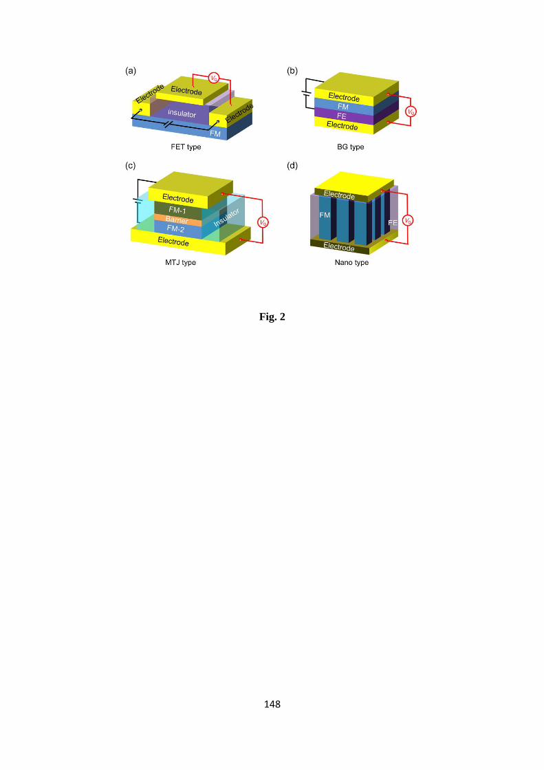
148
Fig. 2

149
Fig. 3

150
Fig. 4

151
Fig. 5

152
Fig. 6
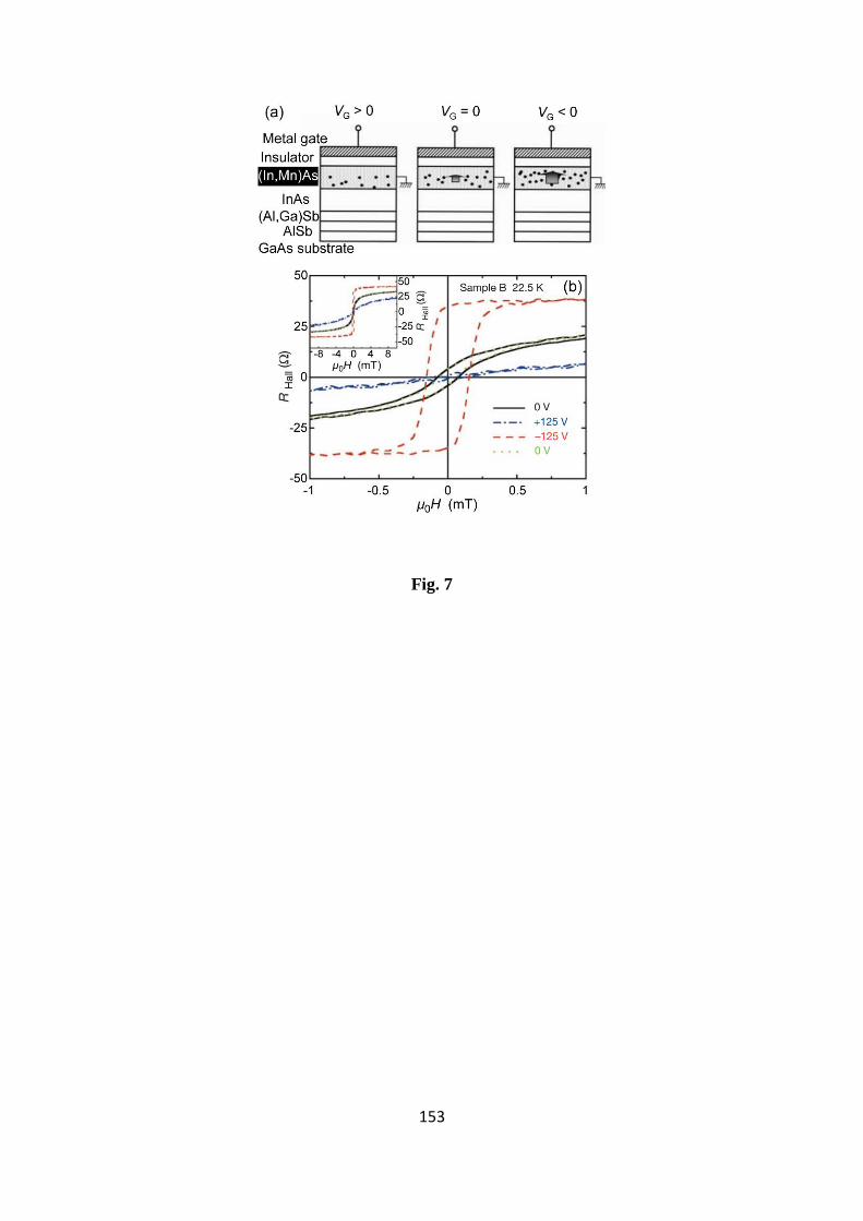
153
Fig. 7
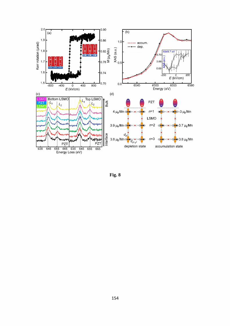
154
Fig. 8

155
Fig. 9

156
Fig. 10

157
Fig. 11

158
Fig. 12

159
Fig. 13

160
Fig. 14

161
Fig. 15

162
Fig. 16

163
Fig. 17

164
Fig. 18

165
Fig. 19

166
Fig. 20

167
Fig. 21

168
Fig. 22

169
Fig. 23

170
Fig. 24
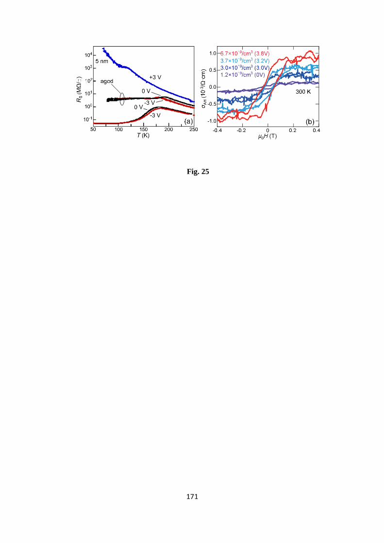
171
Fig. 25

172
Fig. 26

173
Fig. 27

174
Fig. 28

175
Fig. 29
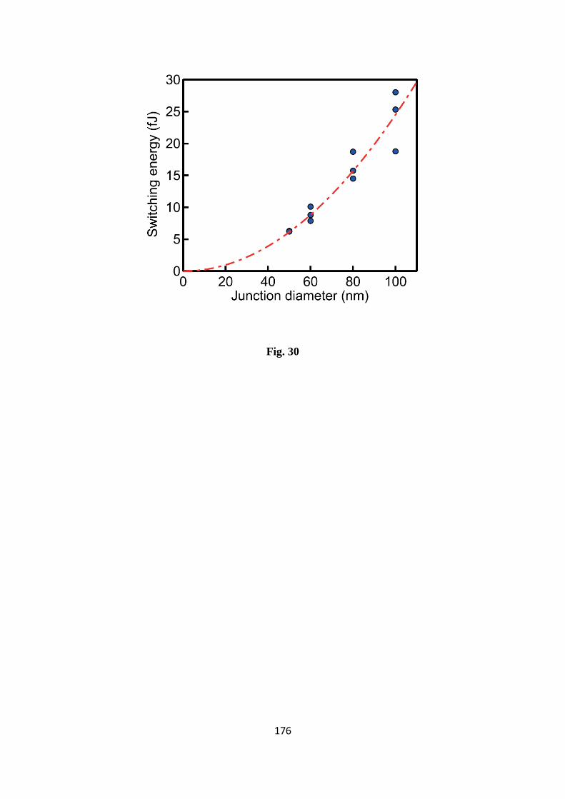
176
Fig. 30

177
Fig. 31

178
Fig. 32

179
Fig. 33

180
Fig. 34

181
Fig. 35