Radiation Design Criteria Handbook - CORE
350
NATIONAL AERONAUTICS AND SPACE AOMlNlSTRATlON Technical Memorandum 33- 763 Radiation Design Criteria Handbook (KASA-CR-1595 13) FAD1 ATIOX DESIGN CRITERIP. N76- 28474 HANDBOOK (Jet Propulsioll Lab.) 349 p HC $10. CL CSCL 20N Unclas G3/33 47648 JET PROPULSION LABORATORY CALIFORNIA INSTITUTE OF T ECHNOLOGY PASADENA, CALIFORNIA August 1, 1976 https://ntrs.nasa.gov/search.jsp?R=19760021386 2020-03-22T14:29:47+00:00Z
-
Upload
khangminh22 -
Category
Documents
-
view
2 -
download
0
Transcript of Radiation Design Criteria Handbook - CORE

NATIONAL A E R O N A U T I C S A N D SPACE A O M l N l S T R A T l O N
Technical Memorandum 33- 763
Radiation Design Criteria Handbook
(KASA-CR-1595 13) F A D 1 ATIOX D E S I G N C R I T E R I P . N76- 28474 HANDBOOK ( J e t P r o p u l s i o l l Lab.) 3 4 9 p HC $10. CL CSCL 20N
Unclas G 3 / 3 3 47648
J E T P R O P U L S I O N L A B O R A T O R Y
C A L I F O R N I A I N S T I T U T E O F T ECHNOLOGY
PASADENA, C A L I F O R N I A
August 1, 1976
https://ntrs.nasa.gov/search.jsp?R=19760021386 2020-03-22T14:29:47+00:00Z
, . 1 , -- ;:*... _ . ---.T .- - .I' - . , - - - ,. - .--.. ..' ' *
i -6'
v
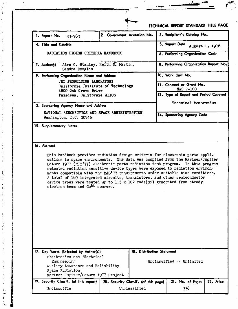
TECHNICAL REPORT STANDUD TITLE PAGE
<
0
I
I i i !
; i 1
r I . [ j " ! i ', E
. . ,--
J
4. Title and Subtitle
RADIATION DESIGN CRITERIA HANDBOOK
7. Author(s) Alen G. Stanley, Keith E. h r t i n , Sandra Douglas
9. Parforming Organization Nane and Address
JET PROPULSION LABORATORY California I n s t i t u t e of Technology 4800 Oak Grove Drive Pasadena, California 91103
12. Sponsoring Agency Name and Address
NATIONAL AERONAUTICS AND SPACE ADMIMISTRATION Washin,ton, D.C. 20546
'* Oat. ~ u g u a t 1, 1976
6. Performing Organization Code
8. PerCwming Organization Report No.
10. Work Unit No.
11 . Contract or Grant No. NAS 7-100
13. Type of Report and Period Covered
Technical Memorandum
14. Sponsoring Agency Code
15. Supplementary Notes
16. Abstract
This handbook provides radiat ion design c r i t e r i a f o r electronic par ts appli- cations i n space environments. The data was cornpiled from the ~ a r i n e r l ~ u ~ i t e r Saturn 1977 !!~JE@'~"T) electronic pa r t s radiat ion test program. I n t h i s program selected radiation-sensitive device types were exposed t o radiat ion environ- ments compatible with the MJS'77 requiremects under stli table b ias conditions. A t o t a l of 189 integrated c i r c u i t s , t r ans i s to re , aad other semiconductor device types were t e s t ed up t o 1.5 x 10⁵ r a d s ( ~ i ) generated from steady electron bean and ~ 0 6 0 sources.
17. Key Words (Selected by Author(s)) Electro,lics ~ n d Elec t r ica l
Eng: neer.il:? Qnality Ac:surance and Rel iabi l i ty Space 3 3 d i h t i ~ ~ l Mariner 7 ~ ~ ~ f t e r / s & t u r n 1977 Project
18. Distribution Statement
Unclassified -- Unlimited
22. Price 21. No. of Page
336
19. Security Classif. (of this report)
Unclassif ie '
20. Security Classif. (of this pap)
Unclassif led

N A T I O N A L A E R O N A l J I I C S A N D S P A C E A D M I N I S T R A T I O N
Technical Memorandum 33- 763
Radiation Design Criteria
Handbook
Alan G. Stanley
Keith E. Martin
Sandra Douglas
J E T P R O P U L S I O N L A B O R A T O R Y
C A L I F O R N I A I N S T I T U T E O F T E C H N O L O G Y
P A S A D E N A . C A L I F O R N I A
August 1, 1976

P R E F A C E
The work described in t h ~ s repor t was performed by the Astr lonics
Division of the Jet Propulsion Laboratory.
JPL Technical Memorandum 3 3 - 7 6 3 k
iii

ACKNOWLEDGMENT
Grateful acknowledgment i s made f o r the contribution t o this r epor t
by perscnnel f rom the Jet Propulsion Labora tory (notably Daniel Bergens,
Merr i l l Burnett, and Alan Yamakawa); The Boeing Co., Physica l Sciences
Section; General Elec t r ic Co., Space Systems Division, Sys tems Survivability
and Reliability Components; and Hughes Aircraf t , Radiation Effects Section.
JPL Technical M c lorandurn 33-763

CONTENTS
. . . . . . . . . . . . . . . . . . . . . Indexof T e s t D e v i c e Types
. . . . . . . . . . . . . . . . . . . . . . . . . . . . I Introduction
. . . . . . . . . I1 Use of the Radiation Handbook in Circui t Design
. . . . . . . . . . . . . . . . . . . . A Bipolar Trans i s to r s
. . . . . . . . . . . . . . . . . . . . . . . . . . b . J F E T 1 s
. . . . . . . . . . . C Diodes. Rectifiers. and Zener Diodes
. . . . . . . . . . . . . . . . . . . . . . . . . D . L i n e a r I C
. . . . . . . . . . . . . . . . . . . . . . . . . . . . E CMOS
. . . . . . . . . . . . . . . . IU I r radia te- Anneal (IRAN) Screening
. . . . . . . . . . . . . . . . . . . . . . . . A Device Types
. . . . . . . . . . . . . . . . . . . . B P r o g r a m Constraints
. . . . . . . . . . . . . . . . . C Experimental Investigation
. . . . . . . . . . . . . . . . . . . . . D IRAN Test Devices
. . . . . . . . . . . . . . . . IV . T e s t Device Types Data Sheets
. . . . . . . . . . . . . . . . . . . . A Bipolar Trans i s to r s
. . . . . . . . . . . . . . . . . . . . . . . . . . B . J F E T 1 s
. . . . . . . . . . . . . . . . . . . . . C Integrated Circui ts
. . . . . . . . . . . . . . . . . . . . . . . . D Zener Diodes
. . . . . . . . . . . . . . . . . . E Constant Current Diodes
. . . . . . . . . . . . . . . . . . . F Diodes and Rect i f ie rs
. . . . . . . . . . . . . . . . . . . . . . . . . . G Capacitors
. . . . . . . . . . . . . . . . . . . . . . . . . . H Res i s to r s
. . . . . . . . . . . . . . . . . . . . . . . I Optical Devices
. . . . . . . . . 1 . Tests Using 0 32-cm (1 18-in ) Space
. . . . . . . . . . . 2 Tests Using 20-cm (d-in.) Space
. . . . . . . . . . . . . . . . . . . . . . 3 Conclusions
. . . . . . . . . . . . . . . . . . . 4 . Tc s t Conditions
J P L Technical Memorandum 33-763

. . . . . . . . . . . . . . . . . . . . . . . . . . . J . CMOS
. . . . . . . . . . . . . . . 1 . Gate Turn-On Voltage
. . . . . . . . . . . . . 3 Transmiss ion Gate Leakage
. . . . . . . . . . . . . . . . . . 5 Propagation Time
. . . . . . . . . . . 6 Dose Rate and Annealing Effects
. . . . . . . . . . . . . . . . . . . . . . 7 Conclusions
. . . . . . . . . . . . . . . . . . . . . . . . . . . . . . References
APPENDIXES
. . . . . . . . . . . . . . . . . A Vendor Identification Code
B . Recomnlended Worst- Case Electronic Device . . . . . . . . . . . . . . . . . . P a r a m e t e r Variations
C . P a r a m e t e r Values of IC Types Requiring Radiation . . . . . . . . . . . . . Acceptance P r i o r to Flight Use
TABLES
1 . Determination of final beta. given initial beta . . . . . . . . . . . . . . . . . . . . . and damage fac tor
. . . . . . . . . . . . . . . . 2 Device type subject to IRAN
. . . . . 3 Lh.1139 quad compara tor radiation tes t sut:lmary-
4 . Electron radiation effects in Zener and . . . . . . . . . . . . . . . . . . . . . r t f c r e n c e diodes
5 . Rejection c r i t e r i a for RCA CivIOS wafer . . . . . . . . . . . . . . . . . . . . radiation sc recning
. . . . . . . . . . . . . . . . . . . . . 6 Analysis of ISS data
. . . . . . . . . . . . . 7 . CMOS wafer screening summary
8 . CMOS radiation cha rac te rization data a t . . . . . . . . . . . . . . . . . . . . . . . . 150 krad(Si)
. . . . . . . . . . . . . . . . . . . . . 9 . Propagation t ime
JPL Technical Memoraadurn 3 3 - 7 6 3

. . . Worst -case p a r a m e t e r va r i a t i ons fo r t r a n s i s t o r s
Wors t -case p a r a m e t e r va r i a t i ons fo r r e s i s t o r s . . . . Worst -case p a r a m e t e r va r i a t i ons fo r fixed capac i to r s . . . . . . . . . . . . . . . . . . . . . . . . Worst -case p a r a m e t e r va r i a t i ons fo r diodes, Zene r d iodes . . . . . . . . . . . . . . . . . . . . . . . Worst -case p a r a m e t e r var ia t ions f o r in tegra ted . . . . . . . . . . . . . . . . . . . . . . . . . c i r c u i t s
it orst-case p a r a m e t e r va r i a t i ons f o r CMOS . . . . . . . . . . . . . . . . . . . integrated c i r c u i t s
. . . . . . . . . . . . . . . . Linear in tegra ted c i r c u i t s
FIGURES
. . . . . . . . . . . . . . . . . . . . . . . Sample shee t
. . . . . . . . . . . Zener voltage change with e n e r g y .
. . . . . . . . . . F l u s angle, e l ec t ron b e a m a t 60 deg
F l u s angle, e l ec t ron b e a m a t 45 deg . . . . . . . N- and P-channel ga tc d r ive t r a n s f e r
. . . . . . . . . . . . . . . . . . . . . c h a r a c t e r i s t i c s
Threshold voltage of N-channel t r a n s i s t o r on . . . . . . . . . . t e s ~ pat tern T.4 6372, preradidt lon
Threshold voltage of N-channel t r a n s i s t o r on . . . . . . . . . . t es t pa t te rn TA 6372, postradiat ion
Threshold voltage of P-channel t r a n s i s t o r on . . . . . . . . . . . t e s t pa t te rn TA 6372, prcrad ia t ion
Threshold voltage of P-channel t r a n s i s t o r on t e s t pat tern TA 6372, postradiat ion . . . . . . . . . . Distr ibut ion of AVGS at IDS a f t e r 1 .5 x 1015 rad(Si) . . . . . . . . . . . . . . . . . . . .
. . . . . . . . . . RCA CD4006, postratl iation, group 1
. . . . . . . . . . LZCA CD-4006, prcrad ia t ion , group 2
. . . . . . . . . . . . . . . . . . LICA CD4006, g roup 3
JPL Tcc!lnical h lemorandani 33-7C 3 vii

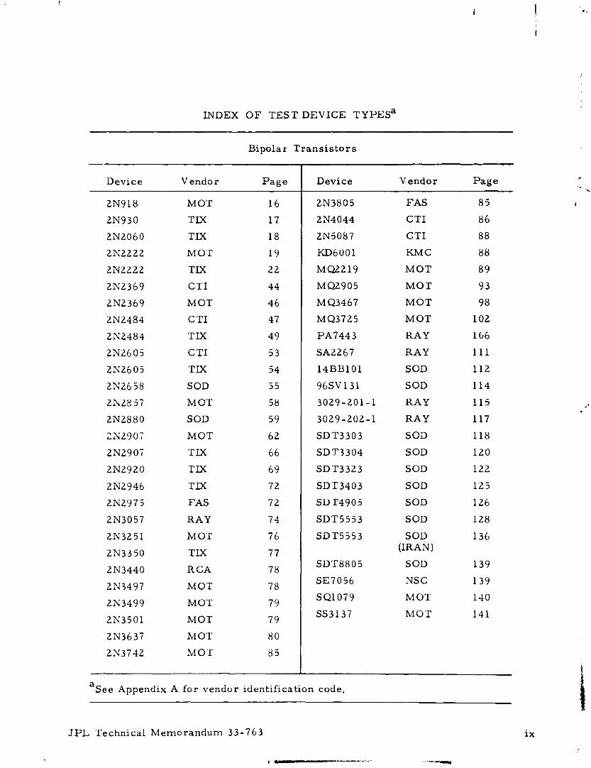
Bipolar
a S e e Appendix A f o r vendor ident i f icat ion code.
T r a n s i s t o r s
.J
-
Device Vendor P a g e
2N918 MOT 16
2N930 TIX 17
2N2060 TIX 18
2N2222 MOT 19
2N2222 TIX 2 2
2N2369 CTI 4 4
2N2369 MOT 46
2N2484 C T I 4 7
2N2484 TIX 49
2N2605 C T I 5 3
2N2605 TIX 54
2N2658 SOD 5 5
2hL2>7 MOT 58
2NZ880 SOD 5 9
2N290; MOT 6 2
2N2907 TIX 6 6
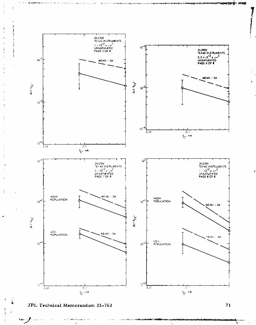
2N2920 TIX 6 3
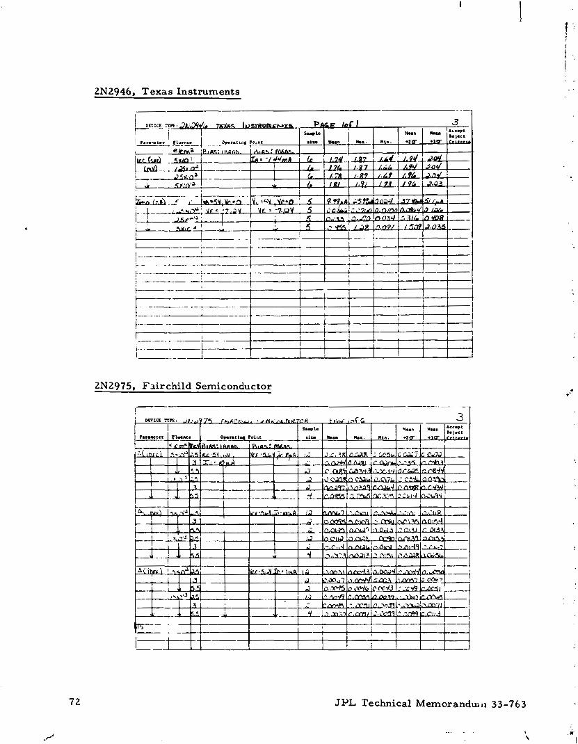
2N2946 TIX 7 2
2N297 5 FAS 7 2
2N3057 RAY 7 4
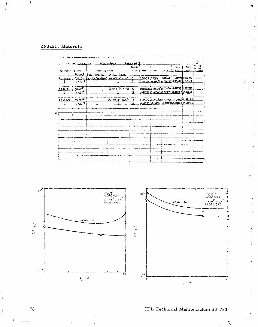
2N3251 MOT 7 6
2N33 50 TIX 7 7
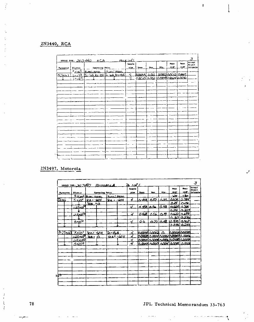
2N3440 R CA 7 8
2N3497 MOT 7 8
2N3499 MOT 7 9
2N3501 MOT 7 9
2N3637 MOT 80
2N3742 MOT 8 5
JPL Technical Memorandum 33-763 i x
Device Vendor P a g e
2N3805 FAS 8 5
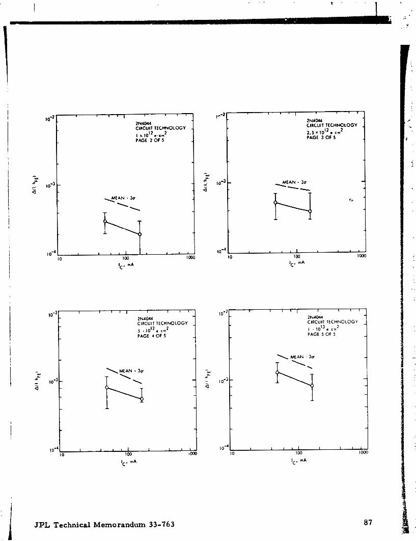
2N4044 C T I 8 6
2N5087 C T I 8 8
KD6001 KMC 88
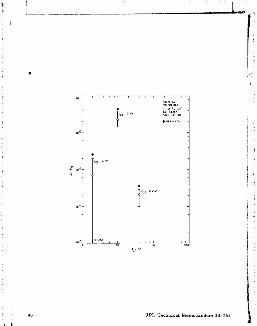
MQ.2219 M O T 8 9
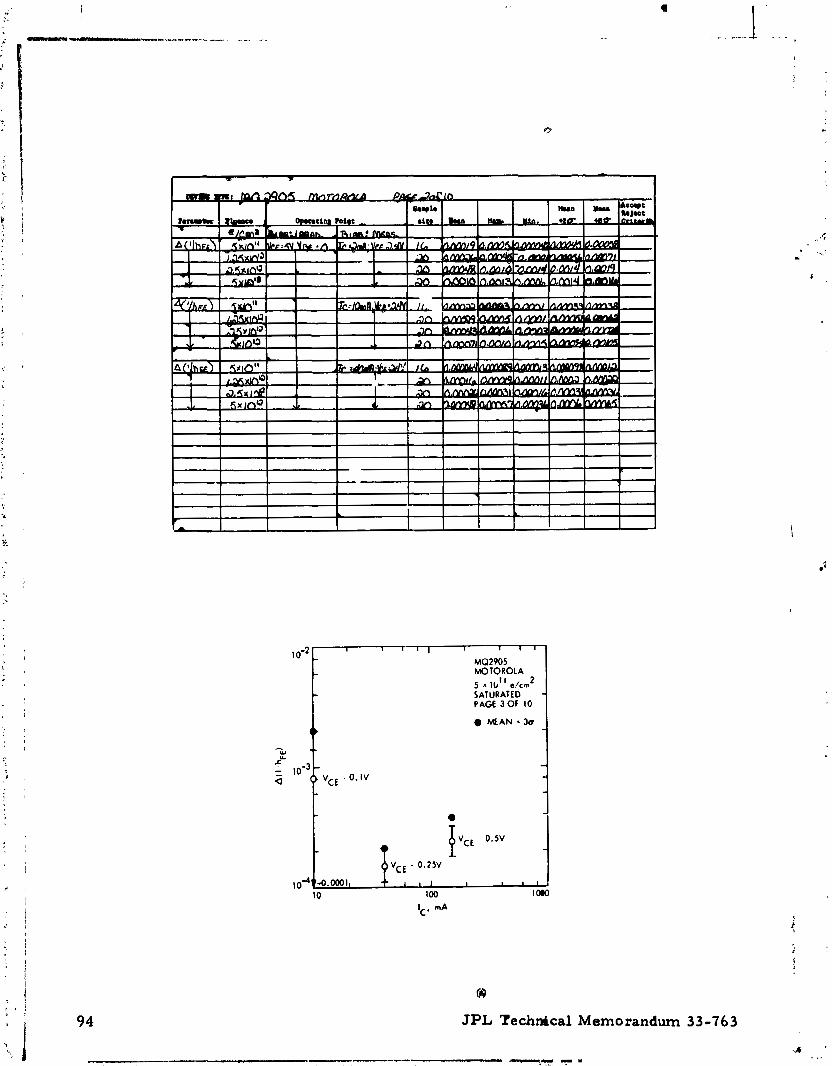
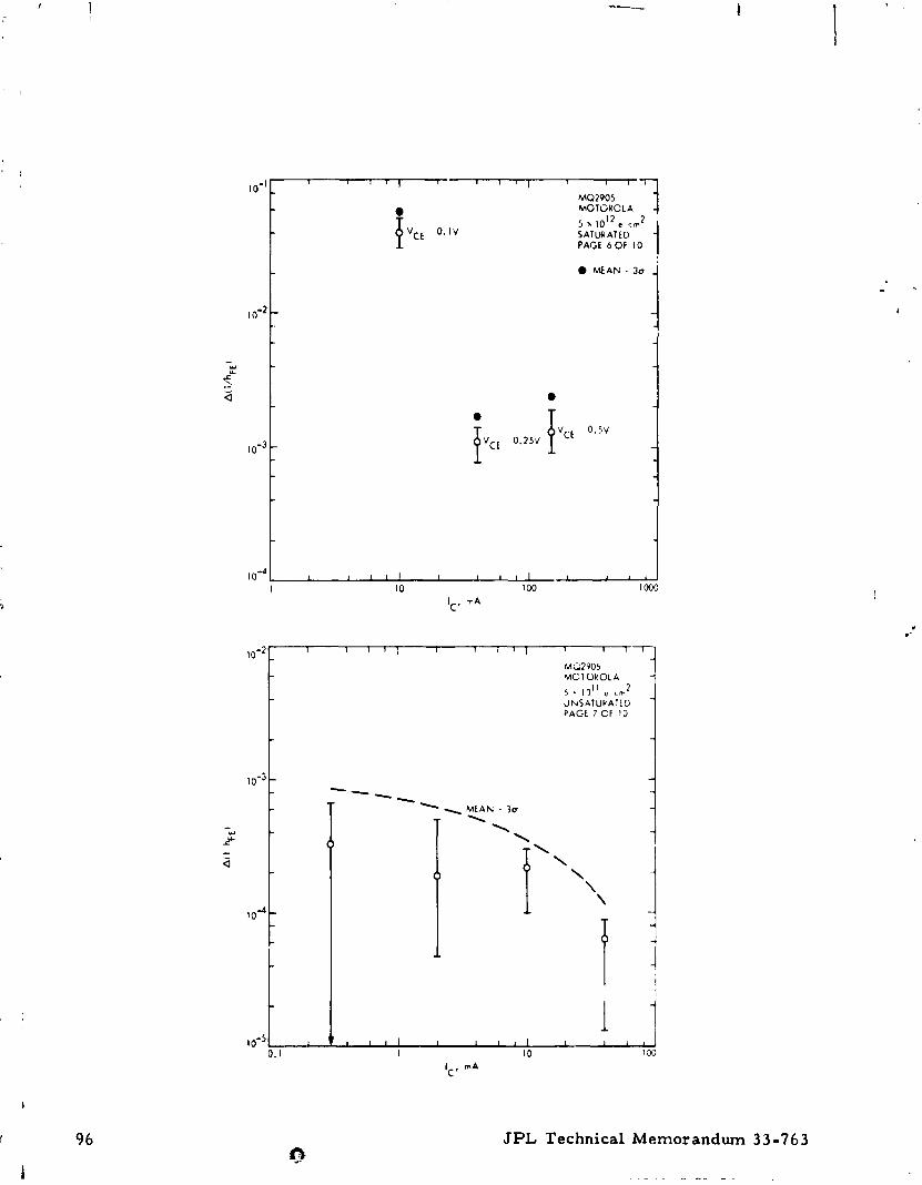
M U 9 0 5 M O T 93
MQ3467 M O T 98
MQ3725 MOT 102
PA7443 RAY 106
SA2267 RAY 111
14BB101 SOD 112
96SV131 SOD 114
3029-201 -1 RAY 115
3029-202-1 RAY 117
SDT3303 S O 3 118
SDT3304 SOD 120
SDT3323 SOD 122
SDT3403 SOD 125
SU I'4905 SOD 126
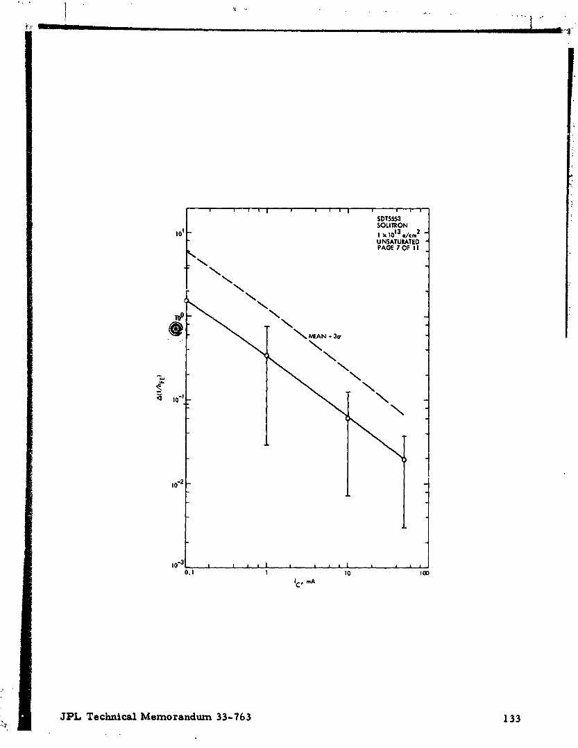
SDT5553 SOD 128
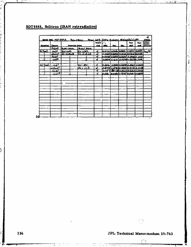
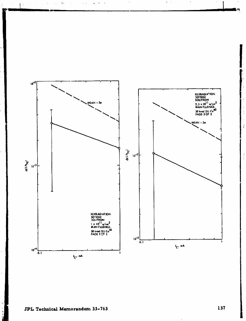
SDT5553 SOD 136 (IRAN )
SDT8805 SOD 139
SE7056 NSC 139
SQl079 MOT 140
SS3 137 MOT 14 1
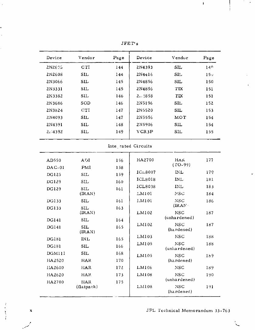
JFE T' s
Device Vendor P a g e
SIL
SIL
SIL
SOD
SLL
SIL
SIL
Device Vendvr Page
SIL
SIL,
SIL
TIX
TIX
SIL
SIL
MOT
SIL
SIL
Inte - rated Ci rcu i t s
A 51
PMI
SIL
SIL
SIL (LRAN ! SIL
SIL (IRAN)
SIL
SIL (IRAN)
IN L
SIL
SIL
HAH
HA& (TO-99)
INL
INL
IPJL
I'? s G
NSC (LRAN .
NSC (unhardened )
NSC (hardened)
NSC
NSC (unlla rdened)
NSC (hardened)
tlA2600 HAR 172 I LM106 NSC 189
lIA262O EIAK LM108 NSZ 190
HA2700 1 IAR (unhardened)
(fla tpack) Lh1108 NSC 191 (ha rdenec!)
x JPL Technical Memorandum 33-763

I n t e g r a t e d C i r c u i t s ( c o n t d )
L M l 1 1 IJSC ( u n h a r d e n e d )
-- - -
Lb1111 NSC W A N )
Device V e n d o r P a g e
LM124 NSC (uni ,ardened)
D e v i c e V e n d o r P a g e
LM124 AS C ( h a r d e n e d )
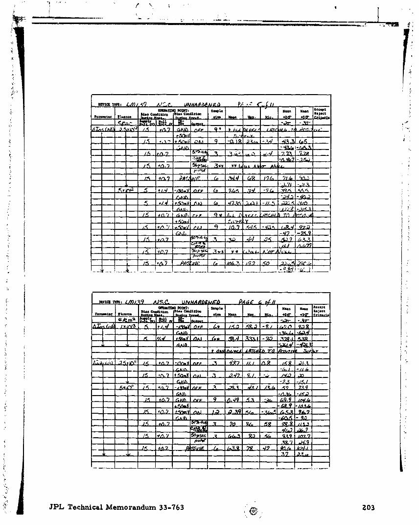
LM139
LM139 NSC ( u n h a r d e n e d )
NSC 2.06 ( h a r d e n e d )
SGN 208
T IX 2 09
NSC 21 1
NSC 212
M O T 213
M O T 21 3
-- -
Z e n e r D i o d e s
MOT
b4OT
MOT
MOT
M O T
DIK
DIK
MOT
DIK
DIK
DIK
MOT
FAS
TRW
MOT
U I'R
U I'R
C o n s t a n t C u r r e n t Diodes
IN5288 MOT 227
1N5290 M O ' r 227
lN5297 MO'I' 228
lN5300 MOT 228
Diodes and R e c t i f i e r s
I
E'J1'1100 FAS 230 1 . *
I J P L rec l in ica l h lemorancium 33-763 d i r

R e s i s t o r s
Capac i to r s
CDP16-01-103G DAL 234 1 LDP16-01-153G DAL 237
Device Vendor P a g e
B l l B CRC 233
CDP16-01-104G DAL 234 1 S! 316-02-473J DAL 237
Device V endo r P a g e
CDP16-01-223J DAL 235 1 MG720 CAD 2 38
CDP16-01-563J DAL 2 3 5
CDP16-01-683J DAL 2 36
CDP18-02-393K DAL 236
MG750 CAD 238
MM125 CAD 239
MS176 CAD 239
Optical Devices
TIL23 TIX
TLL 2 4 r ~ x 240 L S ~ O O T IX 240
CMOS
R CA
R CA
R CA
R CA
RCA
RCA
R CA
RCA
RCA
KCA
R CA
R CA
R CA
R CA
RCA
R CA
R CA
R CA
R CA
R CA
RCA
R CA
RCA
RCA
RCA
K CA
R CA
K CA
K C 4
xii J P L Technical Memorandum 3 3 -763

ABSTRACT
This handbook provides radiation design c r i t ~ r i a for e lec t ronic p a r t s
applications in space environments. The datz was compiled f rom the
hiariner / Jupi ter Saturn 1977 (hlJS177) electronic p a r t s radiatiov t e s t program.
In this p rogram selected radiation-sensitive device types were exposed to
radiat i jn environments compatible with the MJS177 requirements under suit-
able bias conditions. A total of 189 integrated c i rcui t s , t r ans i s to r s , and
other sen,iconductor device types were tested up to 1. 5 x l o 5 rads(Si) 6 0
generatcd f rom steady e lec t ron beam and Co sources .
JPL Technical hiemorandum 3 3 - 7 6 3 xiii

I. INTRODUCTION
In si tu measurements of the Jovian trapped radiation were made by
Pioneer 10 in December 1973 and by Pioneer 11 in December 1974. These
measurements revealed a potentially hazardous environment for M JS'77
spacecraf t e lec t ronics . During 1974 the MJS'77 project c a r r i e d out an
intensive study of the charged par t ic les environment derived f r o m those
measurements and the effects of this environment on both spacecraf t equip-
ment and the Jupi ter encounter a spec t s o: the M JS miss ion. F r o m this
study the ~ a r i n e r , / ~ u ~ i t e r Saturn 1977 Radiat1c.n Control Requirements
Document ( P D 618-229 , dated July 14, 1975) was developed. One of the
requi rements s e t forth i s that the electronic piec? p a r t s used in the space-
craf t pe r fo rm within acceptable l imi ts during and a f t e r Jupi ter encounter
and a t Saturn . Because of r e source limitations, the investigations were
conducted with maximum u s e of existing l i te ra ture and t e s t r e su l t s , limiting
the J P L radiation tes t effort to known o r suspected problem devices where
adequate tes t data \bras not avai lable.
This handbook i s a s u m m a r y of applicable data lesul t ing f r c m the
MJS'77 radiation t e s t effort . The information, presented according to device
type ( s e e Index, page ), i s intended to be useful t o the engineer fo r c i rcui t
design. A complete detailed history file of the tes t resul t s h a s been main-
tained and i s avai lable (contact: A. Stanley in the P a r t s Radiation Group of
J P L Section 36 5) .
In applying the data contained in the handbook, the u s e r should be
aware of inherent l imitat ions; i . e . , the data is intended a s a guide and i s
valid only for the specific manufac tu re r ' s device a t the stated conditions.
lVhen applying the data to c i rcui t designs. the u s e r i s cautioned regarding
extrapolation to lower :luences, different energies and different bias con-
ditions. Device degradation i s sensi t ive to measurement and bias conditions
during i r radia t ion . Also. d i f ferent date codes may reflect p rocess changes
which could change the device sensi t ivi ty to radiation damage.
JPL Technical Memorandum 33-763

Tt.2 radiation environments were in accordance with PD 618-229,
using e lec t rons f rom a Dynamitron a t energies f rom 2 to 2 . 5 MeV, e lec t rons
f rom a \'an de Craff genera tor a t 3 and 5. 5 Me\'. and a cobalt 60 gamma
source . The Dvnamitron was used in those t e s t s wherein the radiation
source i s not identified.
The majo r device t y ~ e s and fea tures of the method used ir! presenting
t e s t resul t s a r e given here in . \Vhenever deviations f rom this fo rm occur
because of the na ture of the data o r resul t s obtained, they a r e fu r the r
described for the specific device o r p a r a m e t e r s involved.
Data f rom different t e s t runs of a given device p a r a m e t e r was com-
bined ~ v h e r e the t e s t s and measurements lvere c a r r i e d out under s i m i l a r
conditions. The data for the follo\ving tes t runs was combined fo r a given
device type:
t 1) Same bias conditions during i r radia t ion .
( 2 ) Same bias conditions during measurzment of p a r a m e t e r s .
( 3 ) Same fluence.
4 Characterizat ion, non-lot sc reen and lot s c r e e n runs.
( 5 ) 2 to 2 . 5 Ate\- electron energy data ( i f o ther energies were used
i t wili be so s ta ted) .
(61 \'CE ( s a t u r ~ l t e d ) for t r a n s i s t o r s .
( 7 \ -CE (not sa tura ted) for t r ans i s to r s .
(8 ) Same manufacturer .
(9 ) Mardened devices.
( 10) Unhardened devices
A sample sheet i s given in F ig . 1, \vith the mhjor fea tures indicated.
.An explanation of those fea tures i s given below.
1 An outl ier i s h e r e defined a s a data point which does not fall
kvithin 3 u of the mean value of that p a r a m e t e r a t the lowest
value of the independent variable ( i . e . , lowest value of the
collector cu r ren t IC o r fluence, where the p a r a m e t e r i s
measured a s a function of I o r fluence, respectively) . C
JPL Technical Memorandum 33-763

JPL Technical Memorandum 33-763

Once established a s an out l ie r in this way, it i s considered a n
outl ier fo r a l l o ther values of the independent var iable .
(21 The data i s calculated both with and without out l ie rs whenever
they exist .
( 3 ) The s tandard deviation cr i s approximated by the following
expression:
where n i s the number of data points, 5 i s the mean value of the
s e t of data points, and x. i s a measured value of the p a r a m e t e r . 1
This gives an unbiased approximaticn of u, including c a s e s where
the sample s i ze ( n ) i s smal l . 1
(4) The p a r t s radiation charac ter iza t ion number evaluates the p a r t s
in accordance with c r i t e r i a f r o m Section VIII of P D 618-229.
These c r i t e r i a a r e repeated h e r e .
Insensitive to radiation; no specia l attention requi red .
Insensitive to radiation except for high-precision
applications. The application and degree of sensitivity
a r e specified.
Sensitive to radiation, resulting in significant degradation
of device p a r a m e t e r s . A radiation screening o r shielding
p rogram i s required if a reasonable design safety marg in
i s lacking.
The device undergoes catastrophic change and i s no longer
functional.
1 See R e f . 1.
JPL Technical Memorandam 3 3 - 7 6 3
F o r t r ans i s to r s , in addition to the tabulated information, graphs a r e
included giving ~ ( l / h ) a s a function of col lector cu r ren t . In these graphs , F E
only those calculated excluding the out l ie rs a r e plotted. The out l ie rs a r e
indicated on the graphs (wherever dual populations occur , both a r e plotted).
11. USE O F THE RADIATION HANDBOOK IN CIRCUIT DESIGN
The data contained in the Radiation Handbook should be used when
performing wors t c a s e analysis of electronic c i rcui t ry . If p a r t s data does
not appear in this handbook, then es t ima tes must be made by Section 365.
The data shows permanent damage to semiconductors in a radiation environ-
ment. The ra t e of impinging radiation o r radiation flux should a l s o be
considered a s this can .:ause a noise effect produced by the impinging
par t ic les on semiconductor devices. In addition, it should a l s o be pointed
out that lclw-energy e lec t rons m a y be deposited and collected by electronic
c i r cu i t ry which can cause a buildup of voltages a c r o s s high res is tance c i rcui t s .
The wors t case analysis i s perfornied by degrading f i r s t fo r t emper -
a t u r e and life (aging) and then fo r radiation to obtain the final degraded
value. The following sections desc r ibe the method of calculating
degradation.
A . BIPOLAR TRANSIS TORS
The cur ren t gain of a t r ans i s to r i s de termined a s descr ibed in the
follo~ving d iagram:
J P L Technical Memoralldum 33-76?
1

Subsys tem Minimum gain r equ i r emen t a t 25 "C, a t IC
Circu i t r equ i r emen t Dera t e f o r t e m p e r a t u r e
I 3 8
h~~~ IC 0.9% p e r "C
f Life dera t ing 25% 28. 5
Minimum t
Radiation dera t ing t
1 /hgE=O. 03 hFE requ i r emen t
I P r e d i c t e d gain 1 5
i Compare r equ i r emen t s with predic t ions and if t h e r e a r e p rob lems , identify
and s tudy solutions.
The radiat ion dera t ing i s de t e rmined by the radiat ion damage
coefficient a ( l / h F E ) , which i s a r e su l t of p a r t s tes t ing . The equation f o r
hFE degrada t ion i s
where
( I ) h ~ ~ ( f i n a l ) i s the predic ted gain t o be applied to the c i r cu i t .
1 2 ) h ~ ~ ( i n i t i a l ) i s the gain a f t e r degrading f o r t e m p e r a t u r e and
life a s p e r the M J S ' 77 Radiation Cont ro ls Requ i r emen t s .
Document 61 8-229, Appendix D ( s e t for th h e r e i n a s Appendix B) .
( 3 ) A ( l / h F E ) i s the radiat ion degrada t ion constant which i s found in
the handbook fo r each p a r t and i s a function of co l l ec to r c u r r e n t
Ic' radiat ion f luence, and b ias conditions during i r r ad i a t ion .
F o r ins tance , a 2N2222A device m a y have the following con-
di t ions f o r which the hFE(final) m u s t be calculated a t
IC = 60 p a (I' C E = 8 1'):
JPL Technical Memorandum 33- 763
--- -.

h ~ ~ ( i n i t i a l ) = 100 a f t e r degrading f o r t e m p e r a t u r e
and life
1 A- = 0.425; m e a n plus 3u at rad ia t ion e l ec t ron h~~ f luence of 5 x 10¹² e l c m 2
1 1 = n- t 1
h ~ ~ ( f inal) h~~ h ~ ~ ( i n i t i a l )
- - 1 h~ ~ ( f inal) + A-
1
h~~ h ~ ~ ( i n i t i a l )
- - h~ ~ ( f inal) 1 0.425 t 100
1 - - h~ ~ ( f inal) - 0.435
= 2.3 which i s s e v c r c clc.,cradatiun in t h c
~ v u r s t c a s e
.JPL Technical Memorandun1 33-763

Under the conditions of I - 20 mA, V C - = 20 v ,
h ~ ~ ( i n i t i a l ) = 100 and a t a fluence of 5 X 1O1':/cm2
using the mean t 3 u value, then h f ~ ( f i n a l ) will be
This demonst ra tes that radiation h a s a much g r e a t e r influence on
t r ans i s to r performance a t ve ry low I therefore , low 1 applications c ; C should be avoided in radiation environments. In power devices th is might be
interpreted to mean that no problems exist , but it i s real ly the e m i t t e r
cu r ren t density that de te rmines the radiation damage. Therefore , power
devices will a l s o degrade severe ly if the emi t t e r cu r ren t density i s low.
The above calculation can be made using Table 1 by going to
a ( l / h F E ) = 0.00441 and hFE = LOO and interpolating to find - -
h ~ ~ ( f i n a l ) = 6 9 . In a l l c a s e s , the hFE of out l ie rs o r maver icks mus t
e i ther be considered o r screened out of lots to be used in ha rdware
expected to encounter radiation environment.
JPL Technical Memorandum 3 3 - 7 6 3

m n ? v . y q m w w o u , O n w O N N W n m - N I ~ ~ ? F E X ' ? ~ % . . - - - 1 - - - - / - - m w ! ~ L : 3 ( o o o m on i ; i d l u i i * i - r ^ N I N N & d = i l d 2 d * l 4 " - r n -- -- - s,.rq; ~ ~ ~ ~ / ~ : a f ; r : r t l ~ ~ ~ ~ ] z r x q 5 1 - - - - D P Z Z J S P C I - - - -
r r c - o o o o o - ~ ~ N I N N - - - - r e
N ~ W W 9 ' - ? 1 m N.':?". r . ? r r ! j L ? $ r z m ~ ( q m 0 - n ~ - ' z 2 z = 1 ~ ~ g X l d s o o m w r r - w r m m U ) - V ) L ? N m r m ' - o o o o - - O N n - r - w N N - - d G d . - c - 0
N m o o . ? r o o " O L ? ? ( 9 q y y " y y q y q q ' 9 9 . ~ " . % 5 , z z = ( s i * d ! & i G d m c r m l m r r - w n o u m m e * m o w a r m o w - o e o r o n n ~ n - r r N N - - N - 0 - - r m
0, W - r - ' O N " - q ? h ! N C : V ! N D f ' ? ? ' ? ' ? l o ? '??N'? ?'-3'!? - Z = r ! ~ ! ~ d $ i / i E O t ~ ~ ~ X Z I P ~ : ~ ! E ~ I : % 0 0 , E Z 2 1 z m
2 y,!qy ' m y ? y q y y y n . ' q ) * . y q q y r . ? ? O N - t - - ~ = g x l - n g g / ~ g g ~ j ~ ~ E : z I ~ : g : : g : : : . g g z z
- - r q y c ? ? n o r*r:c! * T O * r ? o ! * ~ ~ e ~ - r ~ 1 ~ ! ? ? g q q = o o w r n n n n N N - - 0 0 0 0 m m m = i ~ w o r n ~ r o N N N N N N N N N N N N N N N r r . 4 - - - - - - - - & Q + F
m r q r ~ ~ o q r - g =.k2k,5&w
~ 0 ! 9 ~ ! =?=!rq - : * q q i o r ! o * 2 1 9 4 1 - - - I.?!,::: r z z z srrs,zz.I:r , z = , 3 2 2 2
U!rn.Fr. w o n - - q ? w . w , q ? q r . . n y N . 1 o . o e m . n . n m r e . q ~ m 2 z z z z i i i i j i n o n n n n ~ N N ~ N - - - - - - c - - c - - c - c - , 1 1 9 ' 3 C ! S 1 8 z = O z m m m r - r e * &
I I I 8 % o " " I no o i a r w o o - ~ m ~ a / r o o o o o o o o 8 ~ s ~ ~ / ~ ~ s ~ ~ ~ s ~ s ~ s ~ ; . ~ ~ ~ ~ ~ ~ l ~ ~ ~ s ~ ~ s ~ ~ ~ ~ f ~ ,
y y m r Z O Z ) o o w r : = 2 z
' - 1 q y q q l y q y q (O 1 N r - J ) %
g o ! ? ?
JPL Technical Memorandum 33-763
q o y q ~ : ~ q q l y q q q : s . ? ' : q ' q o ? o . $ 1 2 2 2 2 yn(- .q y q q - m r q w 4 r : q o . y ) r ~ ~ ~ ~ l ~ ~ ~ z , s ~ z ~ ~ ~ ~ E z ~ z ~ ~ ~ ~ ~ L z z
n . r q 0 . 0 P z 2 =

The above discussion applies to t ransis tor h when the t ransis tor F E i s not saturated and when i t i s saturated. The saturated hFE, however,
will be much lower because the IB must be greater to lower the
saturation V CE. If, in switching applications, the VCE(sat) must be very
small, then the designer must expect very low resultant h due to low F E initial h and allowances for mavericks. With regard to FE
ICBO' 'BE' and sat)' degrade for temperature and life and then add
additional degradation due to radiation in accordance with this handbook for
the part in question, b e i q careful to select the appropriate bias conditions,
measurement conditions and radiation fluence. In all cases, the t ~ I J
values should be used in the addition. Designers should allow for I CBO as high a s 100 pa, AV a s high i ~ s 0.2 V and AV BE CE(sat) a s high a s 0 .2 V .
B. JFET ' s
The radiation-sensitive parameters of JFET devices a r e the leakage
current I GSS and noise characterist ics. In applying this handbook, the
radiation degradation in I should be added to the efiects of temperature. GSS The noise in the device increases considerably while it i s irradiated but
will probably return to close to original noise characterist ic when radiation
ceases ( i . e . , radiation flux effect). If temperature-degraded I was GSS
calculated to be 0. 5 nA a t VGS = 4 V, VDS = OV, radiation fluence
= 5 X 1 012 e/crn2, and a handbook value of 0 .1 nA, then the total would
be 0 .6 nA.
In N-channel JFET ' s there i s a channeling effect which can cause very
large leakage currents. With no radiation screening controls, this
current ( I ) could be a s high a s 100 nA. GSS
C. DIODES, RECTIFIERS, AND ZENER DIODES
In most applications, diodes and rectif iers do not degrade sufficiently
to provide much concern. However, in applications where the circuit i s
particularly sensitive to forward or reverse characterist ics due to circuit
efficiency, extra care must be taken in the selection of devices with
L Devices that a r e significantly more sensitive to radiation than the others.
JPL Technical Memorandum 33-763
minimum degradation. In these sensitive cases , the degradation i s added
to the parameter degradation with temperature. The parameters in question
a r e V and IR. A V usually changes bv !*a. chan 50 m V in the MJS Jupiter F F environment. I changes by less than 10 FA. 111 the case of sensitive o r
R precision applications of Zener diodes, VZ dope vary with radiation and must
be a c c o u n f ~ d for by adding AllZ due to radiation. AVZ i e l ess than 5 m V in
Zeners less thar, 15 volts; i t i s l ess than 20 rnV in Zeners less than 30 volts.
D. LINEAR IC
The primary parameters of interest a r e VOS, IOS, IBIAS, VOL, and
these a r e highly influenced by a radiation environment. The degradation
values listed in this handbook a r e changes o r delta values due to radiation
effects. These changes should be added to thc othe: changes due to
temperature effects. As a summary of these degradations, refer to
Appendix C.
E. CMOS
The predominant parameters of interest in radiation are:
( 1 ) Propagation delay, which increases with radiation.
( 2 ) Device power consumption, which increases with radiation.
( 3 ) OFF leakages in multiplexers, which increase with radiation.
(4) r ON resistance, which increases with radiation. ds
(5) Noise margin, which increases with radiation.
The effects of radiation a r e added after the effects of temperature and life
a r e determined.
1'0 improve the response of CMOS to radiation, better process
controls must be instituted unless the degradation can be tolerated in the
design. Radiation data should be taken on samples of al l wafers of par ts
to be used in radiation environment. Refer to the data in this handbook on
parts that have been tested.
I \ . *I
JPL Technical Memorandum 33-763
I

I IRRADIATE -ANNEAL (IRAN) SCREENING
An extensive investigation of i rradiat ion-anneal ( IRAN) screening
against total dose radiation effects was c a r r i e d out a s pa r t of a p rogram to
harden the Mar ine r ~ u p i t e r / ~ a t u r n spacecraf t against the Jupi tar radiation
belts. The rret:~od consis ts of i r radia t ing semiconductor devices with
cobalt-60 to a suitable total dose under representat ive bi.as conditions and
separat ing the undesired tail of the d is t r ibut io i~ f r o m the bulk of the pa r t s by
means of a predetermined acceptance l imit . The acceptable deGi?es a r e then
res to red to the i r pi-eirradiation condition by annealing theill at an e:zvated
tempera ture .
Irradiate-anneal i s the only kilown 100% radiation s c r e e n I c : t
maver icks . In general , this should be supplemented by a qualification t e s t
based on a diffusion-metallization lo:, in which a few samples a r e i r r ad ia ted
t o a total dose in excess of the projec t requi rements . Fa i lu re to pass this
tes t implies lot jeopardy and an cxtension of the delivery period by many
months .
Since the lot screening method imposed intolerable t ime const ra in ts ,
i t was hoped that the i r radia te-anneal technique might be employed to
predict the radiation behavior of each device in a quantitative manner s o
that even lots of marginal radiaticn quality might be utilized a t a somewhat
lower yield. This requirement imposes f a r m o r e s e v e r e cons t ra in ts on the
retracking of e lec t r ica l p a r a m e t e r s a f t e r the f i r s t and second i r radia t ion
th tn the elimination of maver icks .
A . DEVICE TYPES
IRAN was considered fo r device types that were determined to be m o r e
radiation-sensitive than allowable by the c i rcui t and shielding analyses .
However, such screening methods work only when the devices show a
significantly varied response to a radiation exposure . The devices consist
of l inear bipolar devices, analog switches, n-channel J F E T s , and bipolar
t r a n s i s t o r s . The p r imary cause of radiation damage induced in these
devices by ionizing radiation i s the formation of inversion l aye r s due to the
JPL Technical Memorandum 33-763
accumulbtion of positive charges in the silicon oxide insulator near the
silicon-silicon oxide interface. This depends on the quality of the oxide,
which i s to a large extent an uncontrolled process variable.
Devices that a r e generically extremely sensitive to ionizing radiatian
( e . g . , MOS devices) a r e poor candidates for the IRAN technique and l lust
be shielded. An additional reason for excluding :dOS devices i s the d i i f i cu l !~
of annealing out the radiation-induced interface states except a t much higher
temperatures. The important LM108 operational amplifier was excluded,
because it had been possible to harden this device against ionizing radiaticn.
All n-channel JFETs with a l ightk doped base region a r e likely to
develop sizab:.. gate leakage currents and were therefore considered to be
candida: s for IR14N. It was considered p r e f e ~ a b l e to redesign circuits , so
that bipolar transistors could operate with minlmum dc current gain rather
than resort to IRAN.
ti. PROGRAM CONSTRAINTS
The original requirement imposed on the devices was to survive a
total dose of 125 krad (Si). This was later decreased to 60 krad (Si) a s the
result of a more precise definition of the Jovian radiation belt. Fo r
reliability reasons. a ceiling of 150°C was imposed on the annealing tem-
perature of the devices. It was la ter discovered that thls temperature i s
inadequate for complete annealing of all surface effects. Burn-in tem-
peratures up to 300°C have been successfully employed in many high
reliability programs, but this requires device construction analysis and
thermal s t r e s s analycis for each device type before procurement. Slich an
irlvestigation was ruled out because of timing constraints. The devices a r e
annealed in an inert atmosphere for 96 hours. Experiments showed that
longer annealing times did not cause any additional annealing.
Yigh-temperature annealing was considered to he unnecessary for
the JFETs . In these devices only the leakage currents a r e affected by the
ionizing radiation. These a r e :asily controlled and not s~gnificant in those
devices that pass the IRAN acceptance cr i ter ia .
JPL Technical Memorandum 33-763 13
' - w - u c . . . a * .J
C. EXPERIMENTAL INVESTIGATION
A ser ies of investigations was carr ied out in order to obtain the
following inf~rmation:
(1) What i s the optimum dose for screening? Too low a dose may
not reproduce the surface effects that cause degradation a t
higher doses; whereas too high a dose degrades the devices
unnecessarily. The onset of surface effects caused by inversion
layers depends on the impurity ccncentration in thc si!icon a s
well a s the composition of the oxide a t the silicon interface
and can therefore not be uniquely determined.
(2) What acceptancl: cr i ter ia can be applied? Unless there i s com-
plete retracking of a l l devices on reirradiation, the acceptance
cri teria musi: be considerably more tightly specified than the
worst case conditions required by the application. On the ot!~er
hand, tight specifications may cause s ~ v e r e yield penalties.
( 3 ) What i s the annealing behavior? Do al l the parameters anneal
completely o r i s there some residual radiation damage? Are
there i .dications of anomalous annealing?
(4) Do the parameters re t ract on reirradiation o r do they exhibit
memory effects? Do any of the devices show anomalous
properties that could not have been predicted from the results
of the f i rs t irradiation?
A ser ies of experiments was conducted on each device type under
consideration for IRAN. Non-flight par ts had previously been exposed to
2 . 5 MeV electrons up to 1013 e / sm2. These devices were annealed for
96 hours at 150°C approximat.!ly two to three months a f te r the initial
exposures. Most parameters ai~nealed back to acceptable specification
levels, but others did not return to their preirradiation values. Since high-
energy electrons can induce a significant amount of displacement damage,
i t was decided to car ry out additional experiments using a cobalt-60 source.
The devices were irradiated to a total dose of either 50 o r 125 krad(Si),
annealed at 150'C for 96 hours a- subsequently reirradiated -with 2 . 5-MeV
electrons, making measurement.; at four radiation levels from 5 X lo1 to
5 x e/cm2.
JPL Technical Memorandum 33-763

D. IRAN TEST DEVICES
Only the flight device types listed in Table 2 were subjected to IRAN;
the other device types tested were unsuitable for IRAN. The degradation that
these devices will experience on reirradiation in the Jupiter environment is
indicated a s a function of f luei~ce in separate tables followicg the normal
radiation properties. After annealing, the dc parameters of a l l devices were
remezsured to the original s~ec i f ica t ion l imits with the following exceptions:
NSC LM101. IB increased from 75 to 100 nA
NSC LM 1 1 1. IB increased from 100 to 400 nA
Ia5 increased from 10 to 2 5 nA
Table 2 . Device type subject to IRAN
IRAN total dose,
Device krad t~ Pe (Si) Acceptance cr i ter ia Annealing
2N4856 60 IGSSatVGS= -20V < 500pA Ncne
2N5196 60 IGSSatVGS=- lOV<100pA None
2N5520 60 IGSS a t VGS = -10V < 100pA None
2N5556 60 IGSS a t VGS = - 15V < 2 50pA None
DG129 50 IS (off) < 3nA 96 h r at 150°C
DG133 50 IS (off) < 3nA 96 h r a t 150°C
DG141 5 G IS (off) < 5nA 96 h r a+ 150°C
LMlOl 125 AVOS<0.7mV, A1 <2.5nA, 0s 96 h r at 150°C
\
i 8 JPL Technical Memorandum 33-763

IV. TEST DEVICE TYPES DATA SHEETS
A . BIPOLAR TRANSISTORS
2N918, Motorola
2N918 MOTOROLA 1 5 . c n PAGE 2 OF 3 I i
Y1 k L
i - G
13) MEAN . 3 0
JPL Technical Memorandum 33-763

2N930. Texas Instruments
2N930 TEXAS INSTRUMENTS
I 1013 e,,cm2 PAGE 3 OF 3
JPL Technical Memorandum 33 - 76 3 17
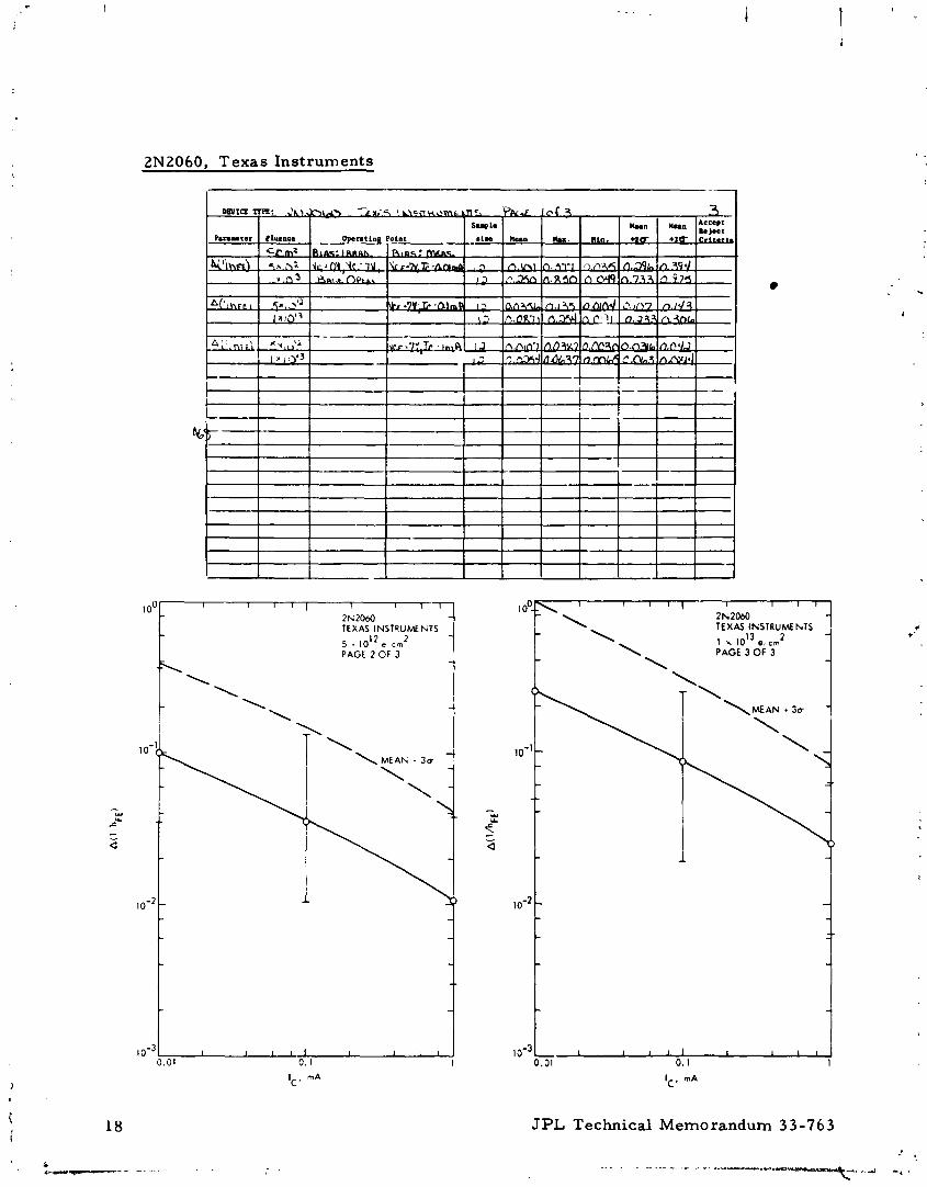
2N2060. Texas Instruments
PAGE 3 OF 3
- -
-
-
- - - -
-
-
JPL Technical Memorandum 3 3 -76 3

2N2222, Motorola
k a s t i r ~ mint
I I B ~ M : I&. L Blm: %6s. -. : - - -! __.,--i !-- - . - .I ! .m : .;16Y7 ,016
I s. rota ! vc . rov I VCL - 0 . 1 ~ : II I
--
la I / .37*8 .d>q I
I I I I --,. 1 .lo1a 1 Vcr =Q.IAV ' 12 f .o le7
b JPL Technical Memorandum 33-763
i * 8b
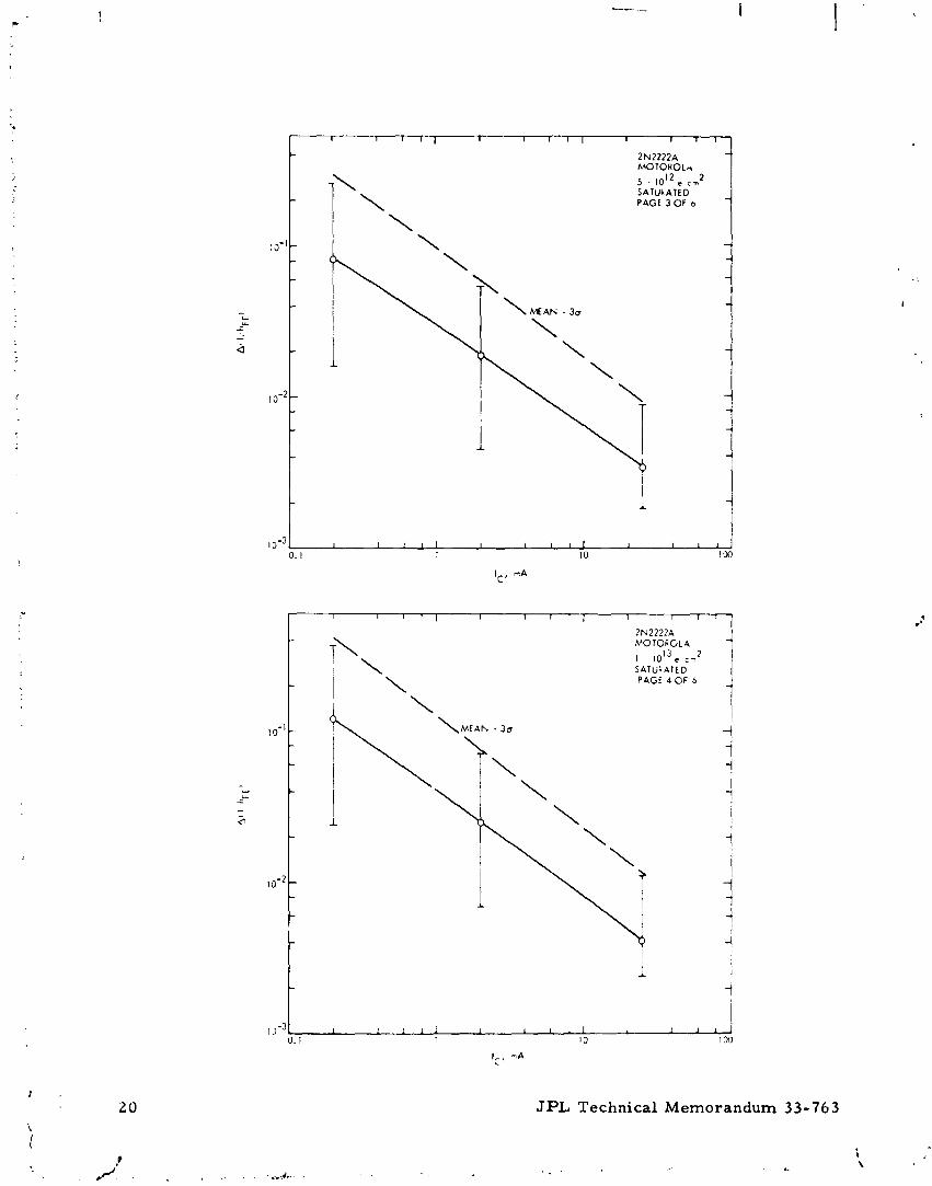
2 N 2 2 2 2 A h4OTOHOLu
5 . 1012 e cm2 SATUhATLD PAGE 3 OF 6
2N2222A M O T O R O L A
I 1 0 I 3 e c n 2 SATUFATED PAGE 4 O F 5
JPL Technical Memorandum 33-763

10-31 I I I l l I I I l l I I I l l I 0.01 0.1 1 10 100
I c e mA
1
\ JPL Technical Memorandum 33-763

2N2222. Texas lnstrumente
Texas Instruments initiated a process change in 1972 affecting the
oxide passivation layer. A s a result, the data for both the tables and graphs
will be grouped a s follows:
Parameter Group Date code range
a(l/hFE) 1 1971 - 1972
> The performance of this type of device at a V - 0. 12 volts is CE -
very unpredictable. The test results a r e questionable because the test
instrumentation did not use separate voltage and current probes. Any small
change in V will cause a very large change in the gain at this operating CE point. Consequently, separate graphs were used for V - 0.1 and 0.12 V
CE - if there was more than one value of V a t a given current level in order CE to prevent overlap of the data due to large e r r o r bars .
2 2 JPL Technical Memorandum 33-763
JPL Technical Memorandum 33-763

JPL Technical Memorandum 33-763


26 R ~ R o D G C I B I L ~ ? I OF THB PACE I6 P m JPL Technical Memorandum 33- 763
I

1.25 . la '?. ,rn2 SATURATLD PAGE In OF 3 7
JPL Technical Memorandum 33-763

JPL Technical Memorandum 33-763
. . . - , - . - - .- .- -. ..~ . a--- -

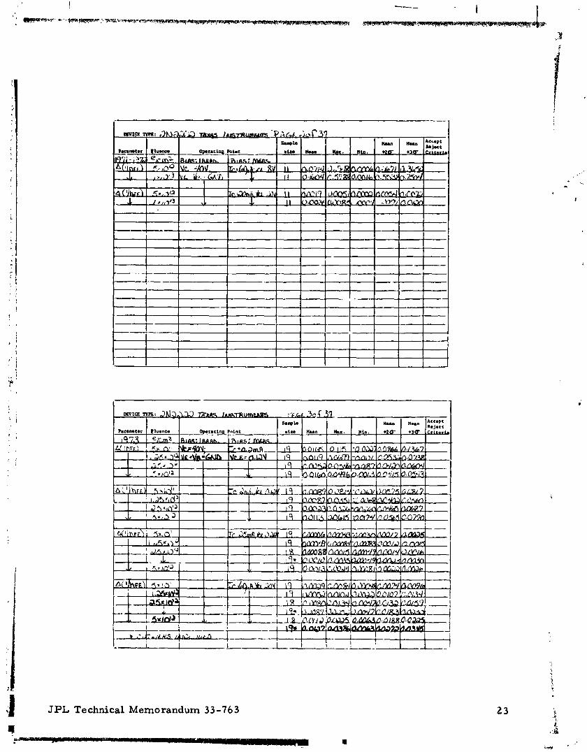
1971-1972 2N2222 TEXAS INSTRIMNTS 5 . l0I2 e , h 2 SATUIIATED PAGE I2 OF 37
a M A N + & 1
JPL Technical Memorandum 33-763 y.

JPL Technical Memorandum 33-76 3

JPL Technical Memorandum 33-763 3 1

JPL Technical Memorandum 33-763
- . . , , \-. '

JPL Technical Memorandum 33-763

JPL Technical Memorandum 33-763


iNfizz TEXAS lNSTRUhlYNTS
5 x 10" .b2 UNSATURATED PAGE 21 OF 37
*= OUTLIER I
, MEAN 317
\
T\ MEAN + 3 0
10-I - , ' 1 I 1 I 8 8 1 I .
1973 2N2222 TEXAS INSTRUMNTS -
JPL Technical Memorandum 33-763
- Y ". L - - a
1.25 . l o t2 a/cm2 UNSATURATED PAGE 22 OF 37
*- OUTLIER
- -
-
I -
I o - ~ I I 1 1 1 1 s * - 0.01 0. I I 10 100

1973
* 2N2222 TEXAS INSTRUMENTS
5 x lot2 e/cw2 UNSATURATED PAGE 24 OF 37
\ dC = OUTLIER
JPL Technical Memorandum 33 - 763

2N2222 TEXAS INSTaUMENTS
5 x 1 o1 ./cm2 SATURATED PAGE 26 OF 37
MEAN + 30
1974-1975 - 2N2222 TEXAS INSTRUMENTS -
JPL Technical Memorandum 33-763
1-1 - . .
10"
5 - I I e/cm2 SATURATED PAGE 25 OF 37
1 \ ... - \
\ MEAN 4 3u -
\ MEAN + 3a -
"4
f ()
a
lo4 -
- VCE 0.26V
-
-
10-S I a I I t I I i l l I I I l l I I I I .
0.01 0. I I 10 100

1974-1975
TEXAS INSTRUMNTS
SATURATED PAGE 27 OF 37
1974- 1975 2N2222 TEXAS INSTRUMENTS 1.25 x 10' e/cm2 SC TURATED PAGE 28 OF 37
MEAN 4 3 u
JPL Technical Mcmorandurn 33-763

loo - I I 1 1 1 I I I 1
1974- 1975 -
- 2N2222 - TEXAS INSTRUMENTS - 1.25 x 10¹² d c m 2 SATURATED PAGE 29 0; 37
- MEAN + 317
10-I - 1 I 1 ' 1 I I I l l I 1---
1976 1975 2N2222 TEXAS INSTRUMENTS
2.5 * l 0 I 2 dcm2 SATURATED PAGE 30 OF 37
• M E A N 4 3 0
i v,, 0.2v lo-= - -
0 - - - P VCE 0.2v
Y r V,, 0.34V - - a \. M E ~ N t 3a ;i [ i V,, 0.26V
I O - ~
I ~-1 1 I 1 1 1 1 1 I 1 1 1 -
0.01 0. I I 10 100 IC . mA
JPL Technical Memorandum 33- 76 3

I I I 1 1 I I I 1 - 1974-1 975 2N2222 - TEXAS INSTRUMENTS 2.5 x 10'~o/crn~ SATURATED PAGE 31 OF 37 1
1974-1975 2N2222 TEXAS INSTRUMNTS
1 5 ,. lob2 e/cm2 SATURATL D PAGE 32 OF 37
1
JPL Technical Memorandum 33- 76 3 4 1
-- ----- -T-

lo0 , I I 1 1 1 1 l l l
1974-1915 -
- 2N5222 - TEXAS I WTRUMENTS - 5 * 1012 doZ - SATURATED PAGE 53 OF 37 - WAN 3v -
I r 1 r 1 I I I 1 1 I I 1 1 1 I I 1 1
1974-1975 2N2222 TEXAS INSTRUMENTS
5 u lo1' 4 c m 2 UNSATURATED PAGE 34 OF 37
JPL Technical Memorandum 33-763 .i

JPL Technical Memorandum 33 -763

1974-1975 -\ \
2N22iZ
\ TEXAS INSRUMMS 5 u 1012 ./cm2 UNSANRATED PAGE 31 OF 37
JPL Technical Memorandum 33-763
v
.- - .-. . --.--- .. . -. .. ---+--a- I.. I
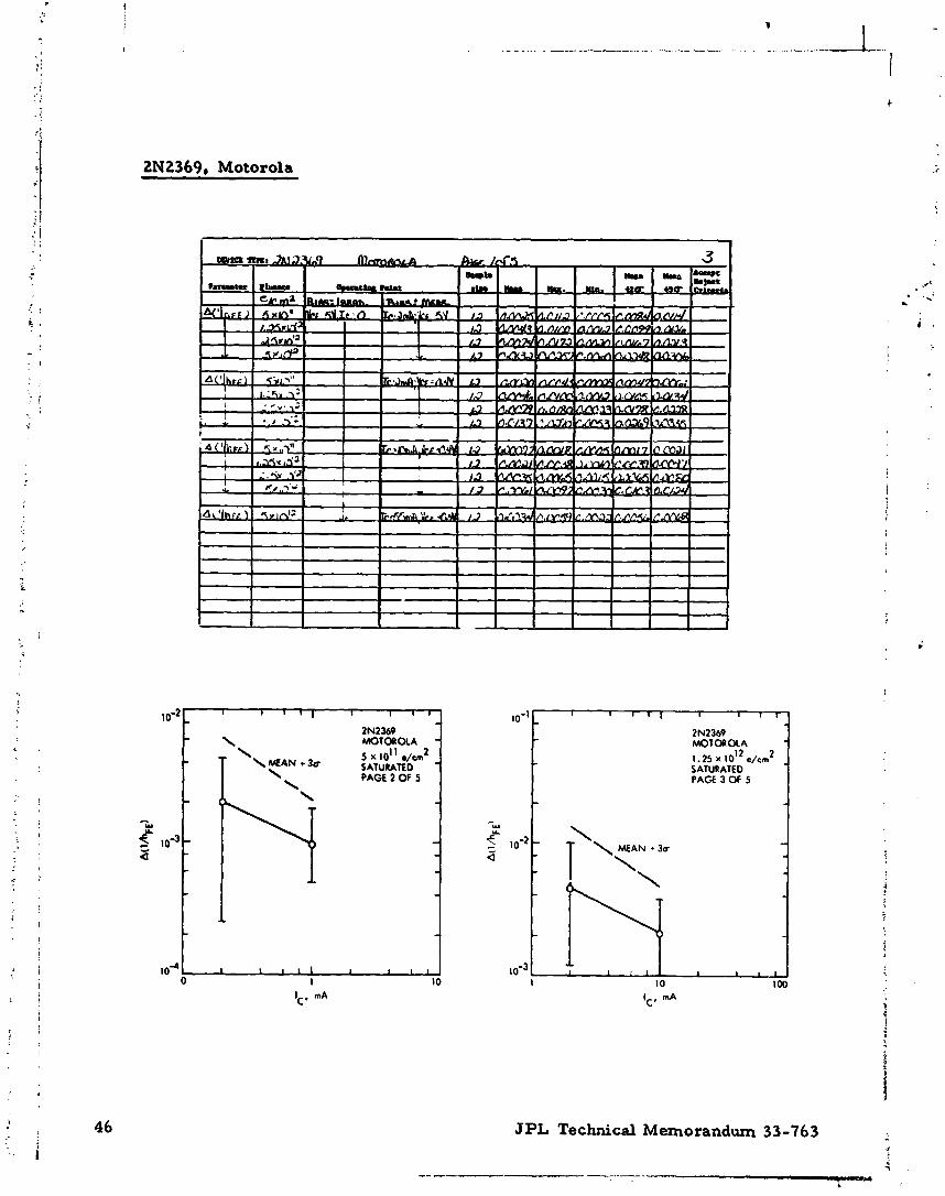
2N2369, Motorola
2N2369 MOTOA'
\ MEAN * 3 0 5 x lo1' CAT1 IDA' --..--- PAGE 2 OF 5
JPL Technical Memorandum 33-763 :
-- -- - -.--.
10-I
- W r 10-2
- I I I l l I I l I f
2N2369 - hn0TrnOCA 1.25x10~~./,,2 - - SATURATED PAGE 3 OF 5
-
- -\ - \ MEAN + 3a
- 4 \
- 10-3 _ I , , I a , 1
A.
I 10 100
10-I - 1 I 1 1 1 I I I I d - 10-I: I I I l l I 1 1 I ' -
2N2369 2N2369 MOTOROLA - - MOTOROLA - 2.5 Y l0I2 e/cm2 - 5 x 10¹² e/m2 - SATURATED
- SAlUUAtED
PAGE 4 OF 5 \ PAGE 5 OF 5 - \ \MEAN 3u
' \ M A N + 3~ U1
f 10-2 z --
lo4 100 I 10 I 10 100
IC, mA lc,
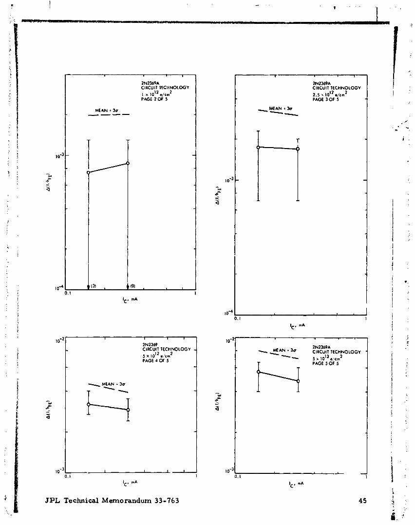
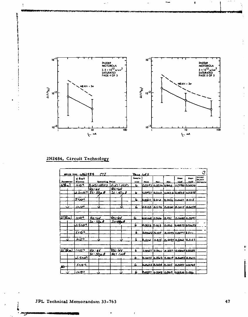
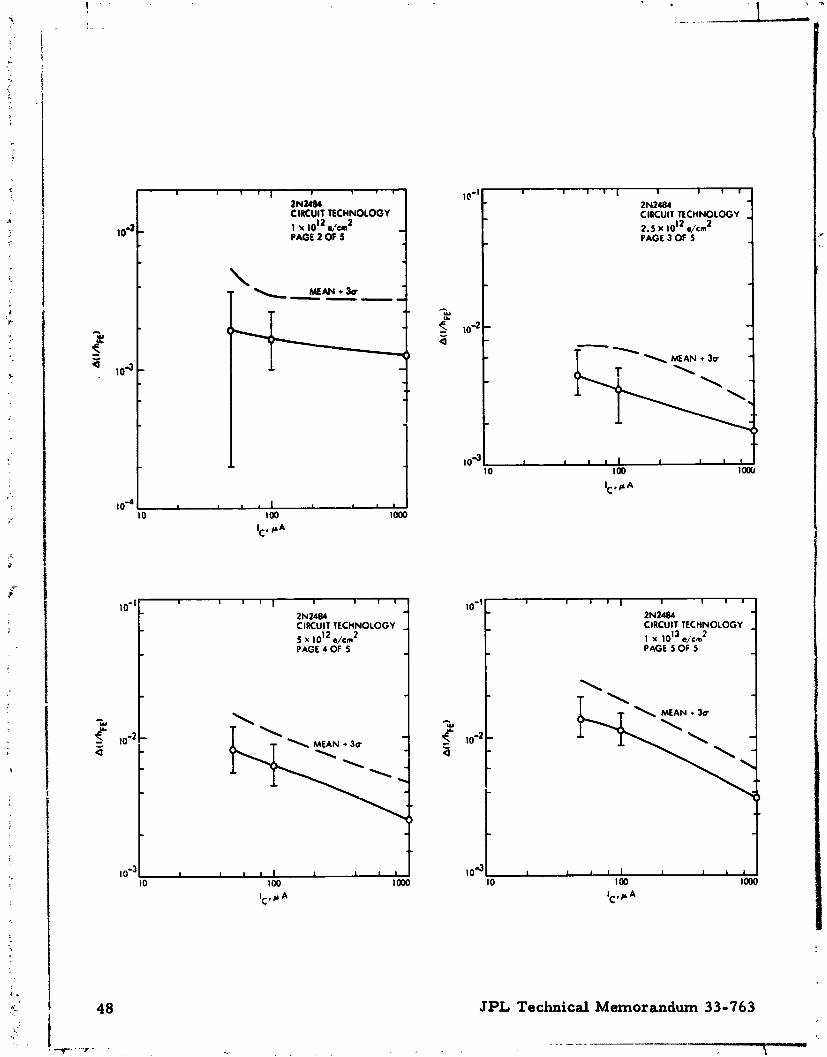
2N2484. Circuit Technoloev
I I JPL Technical Memorandum 33-763
t ' . C
CIRCUIT TECHNOLOGY
5 x e/cm2 PAGE 4 OF 5
Y \ f \
a \ MEAN + 3 0
CIRCUIT TECHNOLOGY 2.5 x 10'' e/crn2 PAGE 3 OF 5
CIRCUIT TECHNOLOGY I r =/em2 PAGE 5 OF 5
JPL Technical Memorandum 33-763

2N2484, Texas Instruments
JPL Technical Memorandum 33-763

! 50 JPL Technical Memorandum 33-763
llll._---ll_- --.-.---- 4 . , . . . , .. ,. . , , . . . x
L - ..Q

JPL Technical Memorandum 33-76;

2N2484 TEXAS INSTRUMENTS
5 10 l2 ./cm2 PAGE 5 OF 5
JPL Technical Memorandum 33-763
---- . . . ,

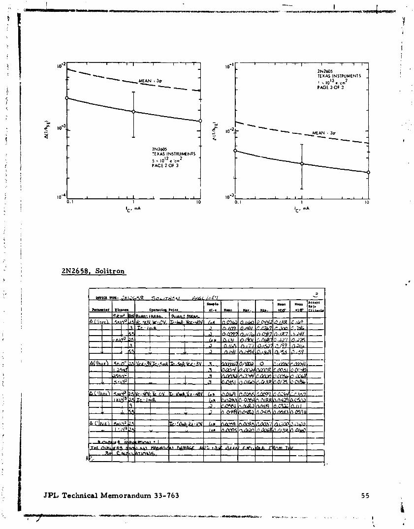
2N26C5, Circuit Technoloav
i i I
I
1 i.
I
JPL Technical Memorandum 33-763 5 3
1.111112

2N2605, Texas Instruments
I 0"
JPL Technical Memorandm 33-763
I
B
- -
I o - ~ A I I l l I I l l L I I I I I 1 .
0.01 2. I I G.01 0. I I
IC, mA IC, mA
I I 1 1 1 1 I 1 1 ' - 2N2605 - - CIRCUIT TECHNOLOGY 1 lo1=.,'cmz
- - PAGE s OF 5 - \
-- '1 -
_ I I 1 1 1 I I I I
2N2605 -
- CIRCUIT TECHNOLOGY , 5 2 1ol2 .,em2
- PAGE 4 OF 5 a
- a
10-I
2N2605 TEXAS INSTRUMENTS
5 . 10l2 c 'cm 2
PACE 2 OF 3 I
2N2658, Solitron
JPL Technical Memorandum 33-763 5 5
2N2605 TEXAS INSTPUMENTS
1 ,. .;em2 PAGE 3 OF 3
-- s, -MEAN 4 317 -- --

JPL Technical Memorandum 33-763
.. . -. - . -- ---- --------- . - -- u

?
4-
lo0 , I I 1 1 1 1 I 1 1 1 1 I I I d - 2N2650 SOLITRON
- - 5 r lo t2 e,,cm2 -
PAGE 4 OF 9
- \
- w 1 i
< - a -
- - - - - - -
- , -
I 0-3 + I I a l l I I I # [ I I # I
1
! 1 10 100 loo0 IC. mA
j 18, I I I I 1 I I 1 1 1 I I I I -
2N2650 - SOLIROK
- - 1 \ ,013 ,. cm2 -
2.5 MeV PAGE 5 OF 7 i -
- 4
4: - I
a
-
l 1 I I l l 1 1 I 1 1 10 Ial
IC. mA
JPL Technical Memo randurn 33 - 76 3 57

SOLITRON I x l0I3 e/cm2
PAGE 6 OF 7
2N2658 SOLITRON
5.5 bbv PAGE 7 OF 7
2N2857, Motorola
3
O~ntiw Point
JPL Technical Memorandru.. 33-763 ! ir
x r.&

2N2U7 MOTOROLA 5 * 10l2 ./,m2 PAGE 2 OF 3
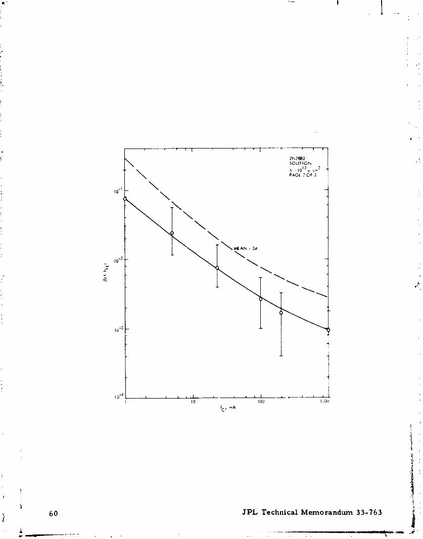
2N2880, Solitron
i
I T i JPL Technical Memorandum 33- 763
B
? .
JPL Technical Memorandum 33-763

' N. I.'.... - ..--. .* . .. ..- ..., ,. . .. -. - . .
f - r
SOLIIRON I x e/cm2 PAGE 3 Of 3
: .
JPL Technical Memorandum 33 - 76 3 6 1 t
4 .. ."%

2N2907, Motorola
JPL Technical Memorandum 33-763 xs
f ,,

I I I I I - I
JPL Technical Memorandum 33-763 63

JPL Technical Memorandum 33-763 i
- 4,

I 1 1 ' 1
MOTOROLA
I z 1013c c n 2 UNSATUk ATED PAGE 7 OF 9
-
C
2h2907A '"7 MOTOROLA
5 . 1 c 2 1 UKSATURATED PAGE 8 OF ?
JPL Technical Memorandum 33-763

2N2907, Texas Instruments
JPL Technical Memorandum 33-763
-a- 3

TEXAS lh;STIU~LhTS
1 . 1 0 ~ ~ . c m
SAIJPi\Tt3 P 4GE 4 CF 9 1
JPL Technical Memorandum 33-76 3

10-2 - 1 I 1 1 ) 1
2 N 2 9 0 7 TEXAS INSTRUMENTS - 5 x l o t 2 c m 2 SATUCATED PAGE 6 OF 9
-
10-1 I 1 I 1 1
2 N 2 9 0 7 TEXAS INSTRUMENTS -
t I , 1013 c cm2 SATURATED PAGE 7 OF Y
2 h 2 9 0 7 TEXAS INSTt U M E h T S
5 . 1 9 " e c T 2 LJhSATUh ATED PAGE 0 OF ? I
JPL Technical Memorandum 33-763

: 7-1
TEXAS IhSTRUhrEhTS
I . ,,? UhSATLlRATET) PAGE 9 OF 9
2N2920. Texas Instruments
1 1 :
\ JPL Technical Memorandum 33-7 6 3

I------ '~WJ ' ' T E X A S I h S R U M E h T S
?.j 10'' c w 2 SATUI. 4 T E C P4GE 3 OF 8 i
JPL Technical Memorandum 33-763
\ HIGH POPULATION
lo-.' 0.01 0.1
Ice mA
1 : k JPL Technical Memorandum 33-763
i 1 ;
2N2320 i t > AS IhSTRUMEhTS
5 . ' m 2 UhSATUKATtO PAGE 70F 8
2N2946, Texas Instruments
2N2975, Fairchild Semiconductor
JPL Technical Memoranduj r l 33-763
.-. - . . +

' A, E JPL Technical Memorandum 33 -763
PAGE 4 OF 5
5 2 . 5 , M E A h 3 0

2N3057, Raytheon
1 L h 2 9 7 5
5 10 r ;n
PAGE 6 Of 6
t2 .5 ) MEAN . 3~ ' 5 . 5 1 M E A h . 3 m
W
JPL Technical Me )randurn 33-763
$ 2 . 5 M ~ L '
- g 3 M c V
$ 5.5 M C . ~
1 I
9 2 . 5 Me'J
I 0 - j G.51 i l 3.01 0.1
- x 3 M c , ;
p i . s h t e 4
- I
IC, mA Ice mA
l a 4

2h3057 LAYTHEON
I 1 0 ~ ~ ~ c n 2
&AN 3u- - PAGE 3 OF 3 --
I I ' " I ' ' I - - 2N$057 RAYTHEON
5 . 1 0 ' ~ ~ c n 2 PAGE 2 OF 3 -
- - - - - 4
- -
lo-2 - d
- - - MEAN -0.00097
i (h4lN 4 . ~ 1 2 6 )
JPL Tech~ical Memorandum 33-763
I O - ~ - -
~-0.000181
- - - - - -
- 10-4
0.01 0. I 1 13 la0 loo0
I C , mA
I 1 1 1 ~ I 1 1 1 ~ I 1 111~ I I l l ? I l l
2N325 1 . Motorola
ZN325 lA MCTOPOLA , 1 \ t. r m'
JPL Technical Memorandum 33-763

2N3350, Texas Instruments
TEXAS INSTRUMENTS
i PAGE ? OF 3
*
* 1
t
2h3~50 TEXAS I ~ S T P U M ~ NTS
1 \ <,-
i PAGE 3 GF 3
* 3
t * GUTLIEPS
JPL Technical Memorandum 33-763 7 7
2N3440, RCA
2N3497, Motorola -
JPL Technical Memorandum 33-763

2N3499. Motorola
2N3501, Motorola
3 PL Technical Memorandum 33 - 7 6 3

lo-' ' \MEAN ~ L T 2lv3Ml MOTOROLQ
5 cm2 , <TLlERS INCLUDED PAGE 2 OF 3
LN3637. Motorola
13-I
JPL Technical Memorandum 33-763
.- . - I
MOIOROLA
5 I O ' ? ~ c m 2 I \ - - \
OUTlllH INCLUDED PAGC 3 OF 3
\ \ MEAh . Jo \

JPL Technical Memorandm~ 33-763 8 1

2N3b37 MOTOROLA 1.25 . 1012 a, cm2 SATURATED PAGi r OF 10
7N3617 MGTOPOLA
RE~RODUCE! lTY OF THE O M m A L pACJ1I IS POO&
JPL Technical M~n.orandum 33-763


2N3637 MOTOROLA
5 \ 10'2 e '"I2
UNSATURATED PAGE 9 OF 10
2h3637 MOTOROLA
1 . UKSATUkATED PAGL 10 OF 10
JPJ Technical Memorandum 33-763

2N3742, Motorola
2N3805, Fairchiid Semiconductor
JPL Technical Memorandum 33-763

2N4044, Circuit Technology
lo-2
JPL Technical Memorandum 33-76 3
. I $ 1 8
2N3805 F AlRCHllD
I 2 2 - 5 . 1 0 e c m PAGE 2 OF 3
1 o - ~ 1
0 .d1 0.1 1
lC, mA
JPL Technical Memorandum 33-763

2N5087, Circuit Technology
KD6001, KMC Semiconductor
JPL Technical Memorandum 33-763

MQ2219, Motorola
ZPL Technical Memorandum 33-763
JPL Tec!mical Memorandum 33-763

MQ2219A * MOTOROLA 1.25 10I2e cmZ SATURATED PAGE 4 OF 10
MEAN + 3o
* OUTLIER 1
JPL Technical Memorandum 33-763
10-I : 1 I 1 1 1 I I I l l I I I 1
- MQ2219A MOTOROLA
- P 2.5 * 1012 efcm 2
VCE = 0. IV SATURATED PAGE 5 OF 10
- MEAN 3u -
1 0 ' ~ - -
- : 1 VCE 0.1'4
," ,I. r - 4 -
- iVCE 0.25" -
I o - ~ I I I l l I , , , I I , k t
I 10 100 r wo IC' mA

10-I - I r I 1 1 I I 1 1 1 I I I I '
- - i MQ22I9A
MOTOROLA - VCE = 0. IV 5 x 1012 cm2
SATURATED - 'PAGE 6OF 10
- 9 MEAN * 3o ,
a
10-2 - 4vcE 0.1" - - -
- Y - u. f - - a - -
I O - ~ - - -
-
-
I o4 I I i l l I I I l l , , I , I 10 100 loo0
Ice mA
MQ2219A MOTOROLA
5 x 10' ' e/cm2 UNSATURATED PAGE 7 OF 10
1 1 1 1 I I I 1
\ MQ2219A MOTORCLA -
\ 1.25 * 1012 cm2
\ UNSATURATED - \
PAGE B OF 10
\ -
T \MEAN + 3u -
- W < zi lo-3- I-. -- - -
- i -
I o ' ~ 0-0.0054 r 1 I 1 I I I I 10 100
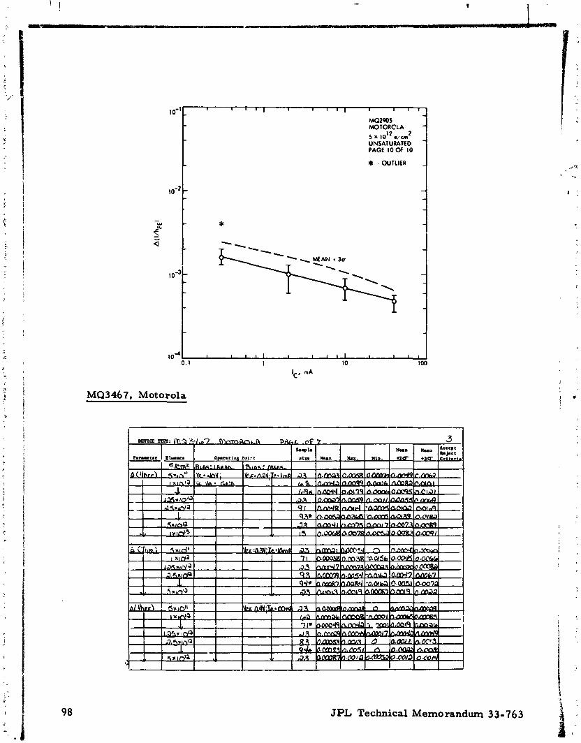
REPRODUCIBILITY OF THE ORIGWAL PAGE I8 POOR JPL Technical Memorandum 33- 763

*TOROLA
2.5 x 10¹² ,/,m2 \MEAN ' 30 UNSATURATED
PAGE 9 OF 10
MQ2905, Motorola
J MQ22l9A MOTOROLA - 5 x lo1? ./,m2 - UNSATURATED
i k JPL Technical Memorandum 33-763
lr
MQ2905 MOTOROLA 5 * lbl' e/cm2 SATURATED PAGE 3 OF 10
@9
JPL Technical Memorandum 33-763

M Q 2 9 0 5 M O T O R O L A i 1 . 2 5 , 1 0 ~ ~ e / c m ~ SATURATED PAGE 4 O F 10 i
M E A N 4 3a -I
MQ2905 M G T O R O L P
2 . 5 r 1012 cm2 SATURATtD PAGE 5 O F 10
ALL VALUES
1 I I 1
I C I 0 0 I(UO
JPL Technical oran and urn 33-763
,
SATURATED PAGE 6 O f 10
M C T O K O L A
5 . ,m2
JPvSATUPATtD P A G L 7 O F 10
JPL Technical Memorandum 33-763
~ - - - -. . - .

MQ2905 MOTOROLA
1.25 . 1012 e Em2
UNSATURATED PAGE 8 OF 10
!
MQ2905 ArOTOROLA
2.5 h 10IZ e/cm2 UNSATURATED PAGE 9 OF 10 1
JPL Technical Memorandum 33-763
' 1 -
. . /'
10-I:
r:
I 1 0 - ~
i 1 j -
i W
j 5 z i i "
I _I i - < . , 1 o - ~
/ ; ,
- I ' I
1 o - ~
. , IC. mA ! I t -
r j I
MQ3467, Motorola I I i I
I
' I
I
I
J i i j i i ; 1
i f , .
I J ' .
, .
I i
P
,. . P
I JPL Technical Memorandum 33-763
I
1 I 1 , I 1 I I I ( 1 I I I ' - MQ2905 MOTORCLA - ~ X I O ~ ~ . , , ~ ~ - - UNSATURATED
PAGE 10 OF 10
- * : OUTLIER -
- - - - -
- * -
- -MEAN * 3 0 : :: - -
I I I M i I I I l l I I M I
0.1 1 10 100
...' x \
r :
, . . .

JPL Technical Memorr: durn 33-763

MOTOkOLA
1.25 x 10¹² c c m
PAGE 5 OF 7
JPL Technical Memorandum 33-\ 63
- - -, -

7---- I I I 1 I r 1 1 1
MOTOROLA
2.5 . 10" c c m PAGE b OF 7
hnOTOhOL4
5 1012 < c m 2
PAGE : OF I i

MQ3725, Motorola
REPWDUCBlLITY OF TIIE] OKIGR3AL PACE I6 POOR JPL Technical Memorandum 33-763
!!

JPL Technical Memorandum 33-763

JPL Technical Memorandum 33-763
--- lo-) ' 7 1 r - 7 - r
\ MQ3725 MOTOROLA
\ VCE O.ZV 1 1ol2. ,m2 -
\ PAGE 5 OF 9
- u tA
L - a
io-" -0.0lb3 1
!
4
I
I
10 1170 o -A 11)w IC, m i *
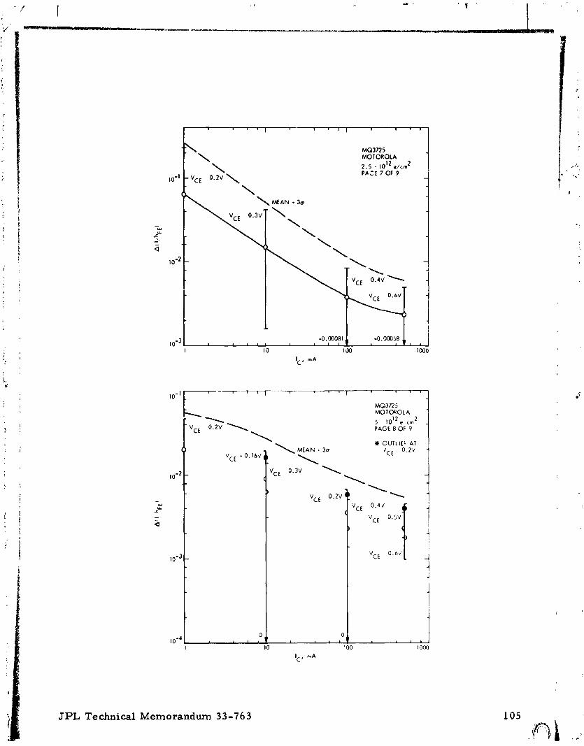
MQ3725 MOTOROLA
2 . 5 . 1012 al/cm2 PrcE 7 OF 9 i
JPL Technical Memorandum 33-763

PA7443, Raytheon
MOTOROLA I l o13 ./m2 PAGE 9 OF 9
MEAN * 3 0 4
JPL Technical Memorandum 33-763

JPL Technical Memorandum 33-763

PA7443 RAYTHEON 5 x 10" e/cm2 SATURATED PAGE 4 OF 9
a
PA7443 RAYTHEON 1 . e/cm2 SATURATED PAGE 5 OF 9
- w
f - 10-3,: a
I o - ~
JPL Technical Memorandum 33-763
I I
10 100 loo0
J
Vcf = 0.4V
- VcE : 0.3V I ~ v c E o . . . - MEAN - 0 M I N : 4.00079 -0.00004

PA7443 RAY1 HEON
10-2 - tb 1.25 loi2 e/cm
SATURATLD T
VCE = 0.2V PAGE 5 OF 9
(1
' VCE - 0.4V
T, VCE - 0.3'1
Y
5 ?j - I . ' ? vcE = -4
I 1 -0.00032
1 1 I 1 L-
I 10 1 oil _1 1000
f + OUTLIERS
PA7443 RAYTHEOt:
1.25 r 1012 e/cm2 SATURATED PAGE 7 OF 9
JPL Technical Memorandum 33-763 F

JPL Technical Memorandum 33 -763

SA2267, Raytheon
JPL Technical Memorandum 33-763
I I I l l I 1 I I * 10-I
I
SA2267 RAYTHEON - 2.5 x 10¹² e/cm2
10-2,
a
P4G; 3 CF 5
- * OUTLIER - M A N + 3 0 - 3
- -
-
c
10-2 t -
SA2267 r RAYTHEON -
I 101
f t
"
VCE 0.4V -
y1
f ( t z
t PAGE 2 OF 5 -
3 - (b
- k u
* OUTLIER - /*AN 4 3q - 0vCE = 0.2V
10-4 I , , ; , o - 3 , ~ . ~ ~ q 4.0024 -0.0169 1 - 8 d 1 I I T I 1 1
I 10 I W 1 10 100
Ice mA Ice mA
\tCICC 0.3V
- -0.0188
- - - (b
vc, = 0.2v
- vcE - 0 . 4 ~ 9
() VCE = O.3V -

lo-' - I I 1 1 1 I I I 1 - $A2267 - RAYTHEON - 5 x lo1* ./m2 - -
\ PAGE 4 OF 5
\ '. - \ M A N + 3 0
- a . --
14BB 10 1, Solitron
JPL Technical Memorandum 33-763

- I- I I 1
1488101 SOLITRON
I \ e cm2
\ VCE SATURATED
PAGE 2 OF 5
1488101 SoLIlKOrJ
12 2 5 2 I0 e c n VCE SATURATED
PAGE 4 OF 5
MEAN 30 -----
1488101 SOLITRON
2.5 10li c. cm 2
VCE SATURATED
PAGE 3 OF 5
JPL Technical Memorandum 33-763 1 ' .
5; +
I 0-I I I 1
1488lOl SOLITRON
I =, cm2 VCE SATURATED
PAGE 5 OF 5
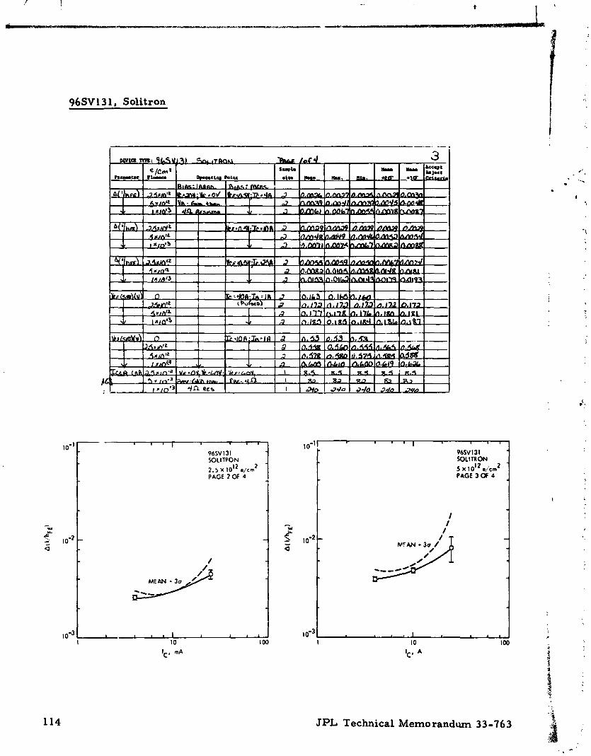
96SVl3 1, Solitron
96SV131 SOLlfPON
2.5 X 10¹² e/cm2 PAGE 2 OF 4
JPL Technical Memorandum 33-763

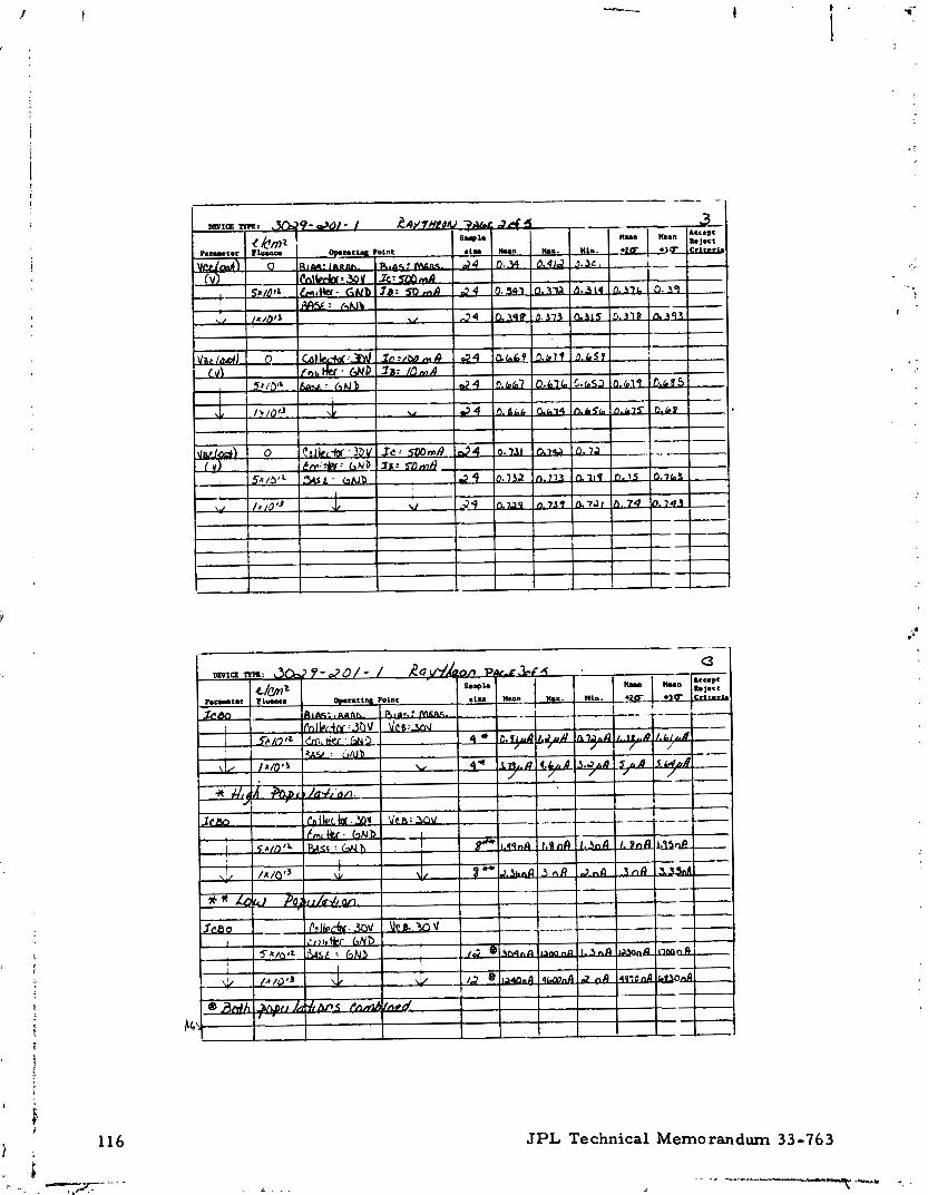
3029-201 -1, Raytheon *
1 96SV I3 I SOLITRON I lot3 - PAGE 4 OF 4
MEAN t 3u !9. - -
I o - ~ 1 1 I I
1 10 loo IC' A
JPL Technical Memorandum 33-763
- - - - ------ . . Ta-* -,

3029-202- 1 , Raytheon
10-I-. 1 1 I
3029-201-1 RAYTHEON 1 1013 e,,cm2 . PAGE 5 OF 5
\
JPL Technical Memorandum 33-763
-
0
-
,lo)
/-
-
10 100 1000
Ice mA
I o - ~ I A

3029-202-1 RAYTHEON
5 > c cm2 PAGE 2 OF 3
3029-202- 1 RAYTHEON
I r dCm2 PAGE 3 OF 3
SDT3303, Solitron
JPL Technical Memorandum 33-763
. . .-. -- .- - " ------ --" i " . *;

5 . 1 0 " e cm' PAGE 3 OF 4
- - - M E A N + 3s -- ---
JPL Technical Memorandum 33-763

10-I - I I 1 1 1 I I 1 1 1 I I I l l I 1
SOT3303 -
- SOLITRON - I - PAGE4OF4 -
- - - g 10-2- z -
- -
- -
10-3 a I I l l I I 1 1 ~ I I I # I I 10 1w 1000
IC, mA
SDT3304, Solitron
JPL Technical Memorandum 33-763

10" - I I 1 1 1 I I I I 1 I I I 1
SDT3304 -
SOLITRON - 5 \ l 0 l 2 e/cm2
- PAGE2OF3 -
5DT3304 SOLITRON
I y loi3 c / c m 2
PAGE 3 OF 3
JPL Technical Memorandum 33-763
L * '-
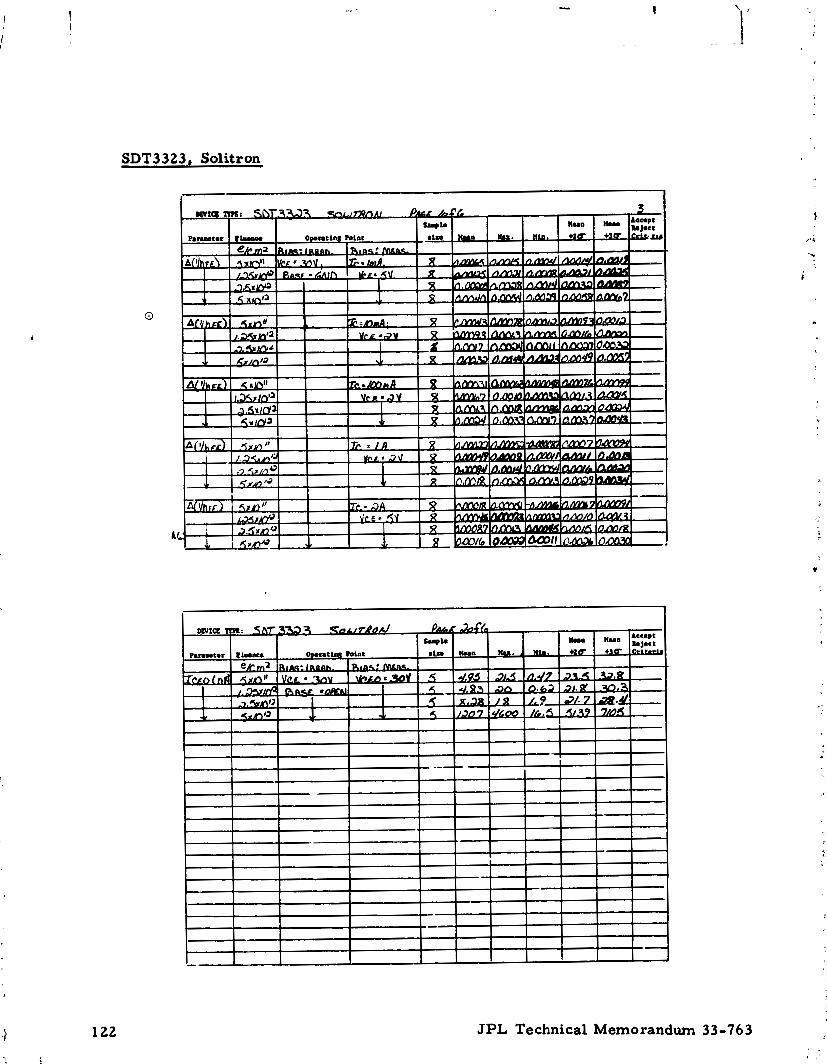
SDT3323, Solitron
JPL Technical Memorandum 33-763

SDT3323 SOLITRON 5 w lo1' ,/,m2 PAGE 3 OF 6
SD?D23 SOLITRON -1 1.25 x 10¹² e/cm2 PAGE 4 OF 6 4
!
JPL Technical Memorandum 33-76; 5

5073323 SOLIAON 2.5 X 10¹² e/cm2 PAGE 5 OF o
10-2 - 1 -1
- LU ------ M A N t 3 7 < - ----- . -- a - --
t r -- -.. ----
1 0
lo4 - .A -r..Y-f - -
lo4. I I a l l I I I l l I I I l l I I # 1
I 10 100 1000 loo00
LDT332, SOLITRON 5 1 10l2 ./cm2 PF >C 6 OF 6 i I
JPL Technical Memorandum 33-763
- , - - * ,*;
JPL Technical Memorandum 33-763
9
10-I 1 I I I 1 I I I I
SOT3103 SOLITRON 5 x l 0 ~ ~ e / c r n ~ - PAGE 2 OF 4
lo-2 - ' \U*N +3t, -
1 0 ' ~ 1 a I I I 1 1 1 .
10
id loo lrn
IC' '"A

JPL Technical Memo randurn 33-763


- _ - . . _ % _ . . . - - ._ - - * - ' , 3 . - - . . , .. . . . - .. ::- -. . , . .. -. . - . . - . . . - .. . . -- - - -. . ..- -. . - . - - - - - - .-. . - -
JPL Technical Meunoranclun~ 33-7 6 3
IL Ire m- 11-I
JPL Technical Memorandum 33- 763
- . . I 1 1 1 1 1 8 -
JPL T e b i c d Memorandum 33-763


132 JPL Technical Memorandum 33-763
JPL Technical Memorandum 33-76 3

JPL Technical Memorandum 33-763

JPL Technical Memorandum 33-763
I:
..g
. . , i.
Wi
, 6;
I:'
p
<
p
i! - ?
I.
I '
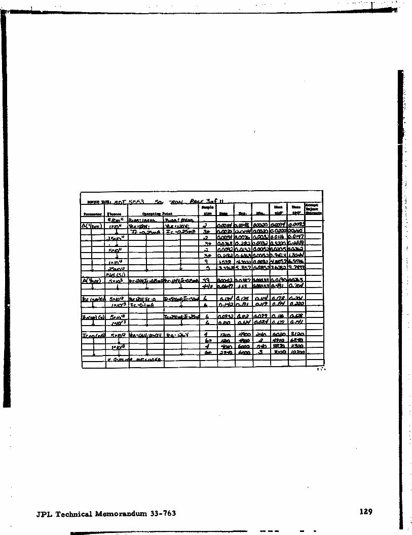
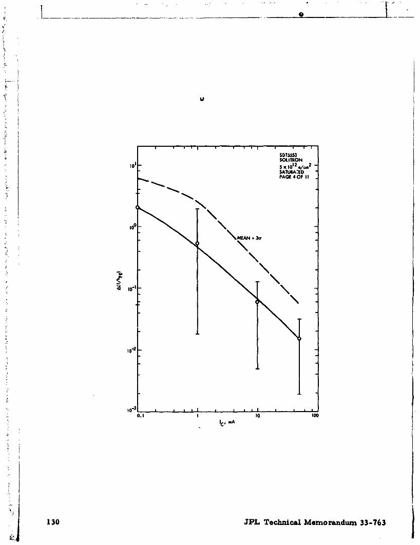
SDTS553, Selitron (IRAN reirradiation)
JPL Technical Memorandum 33-763
JPL Technical Memorandum 33- 763

JPL Technical Memorandum 33- 56 ?!
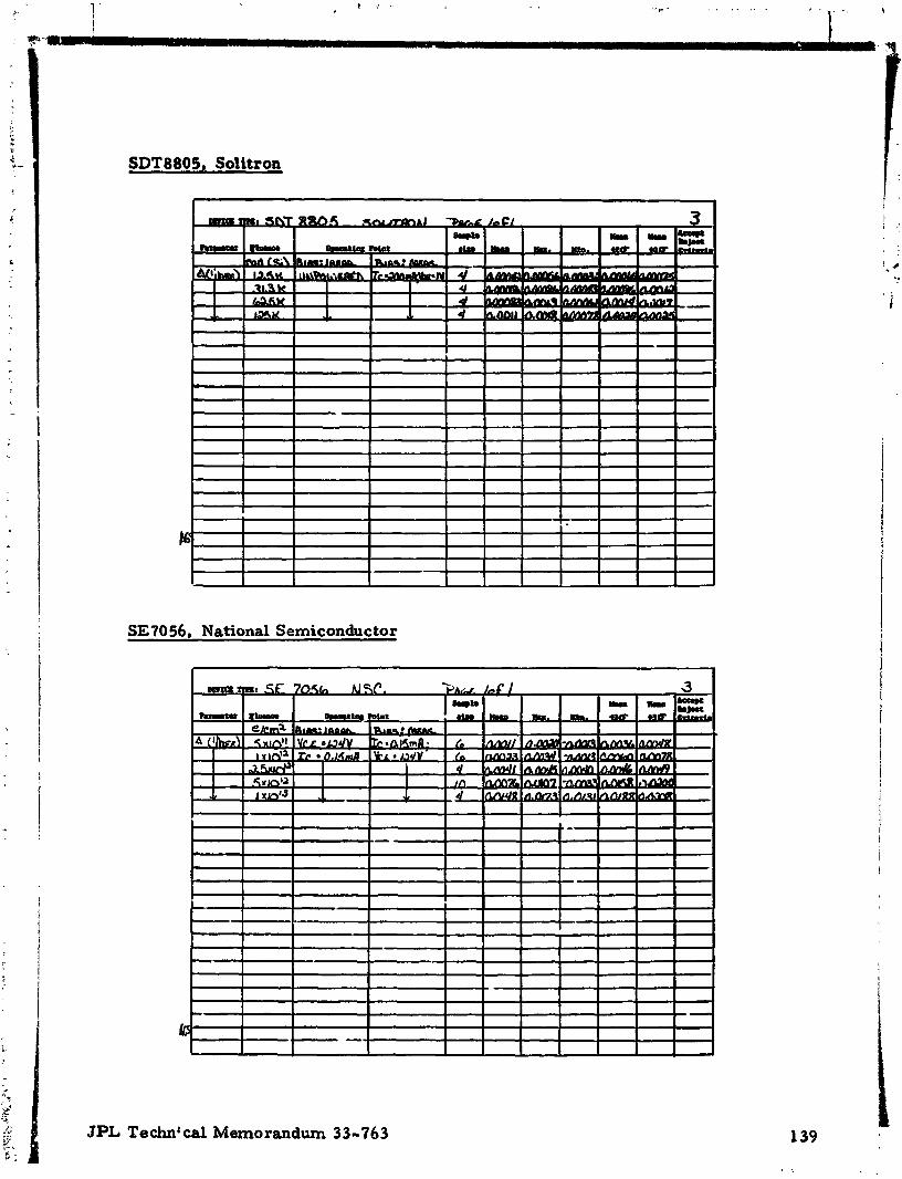
SDT8805, Solitron
SE7056, National Semiconductor

SQ 1099, Motorola
JPL Tech- ical Memorandum 33-76 3
. . . - - . -. . . .. . ., , - ----------
,, , . -.- . '

PAGEIOF4 .
M A N 38 -----3-,-->
I
JPL Technical Memorandum 33-763

142 JPL Technical Memorandum 33 -76 3
- 6 ' , . f . ..
------- - .. .. ' ' . - m .


b
. - .. . -- I ' ' ' ;
.
B. JFETe d
2N2608, Circuit Technology
- .d. * -. -
, .
i
I : I ;
1 : 4
i
2N2608, Siliconix
I 1 '; 1 i
d i I ; I . ~
T 1
$
JPL Technical Memorandum 33-763
--- - - .. - ----- ." --- - , .

2N3066, Silicanix
2N333 1 , Siliconix
JPL Technical Memorandum 33- 763

2N3382, Siliconix
2N3686, Solitron -
. ~ - I' . ~- 1' . - -. 1
I : I .
/ i
i I i i i I
j I I
4 I i I j
4
1
n i
0
1
I * I : 1 ; i , I
I i i
JPL Technical Memorandum 33-763

2N3824, Circuit Technoloa
2N4093. Siliconix
JPL Technical Memorandum 33-763
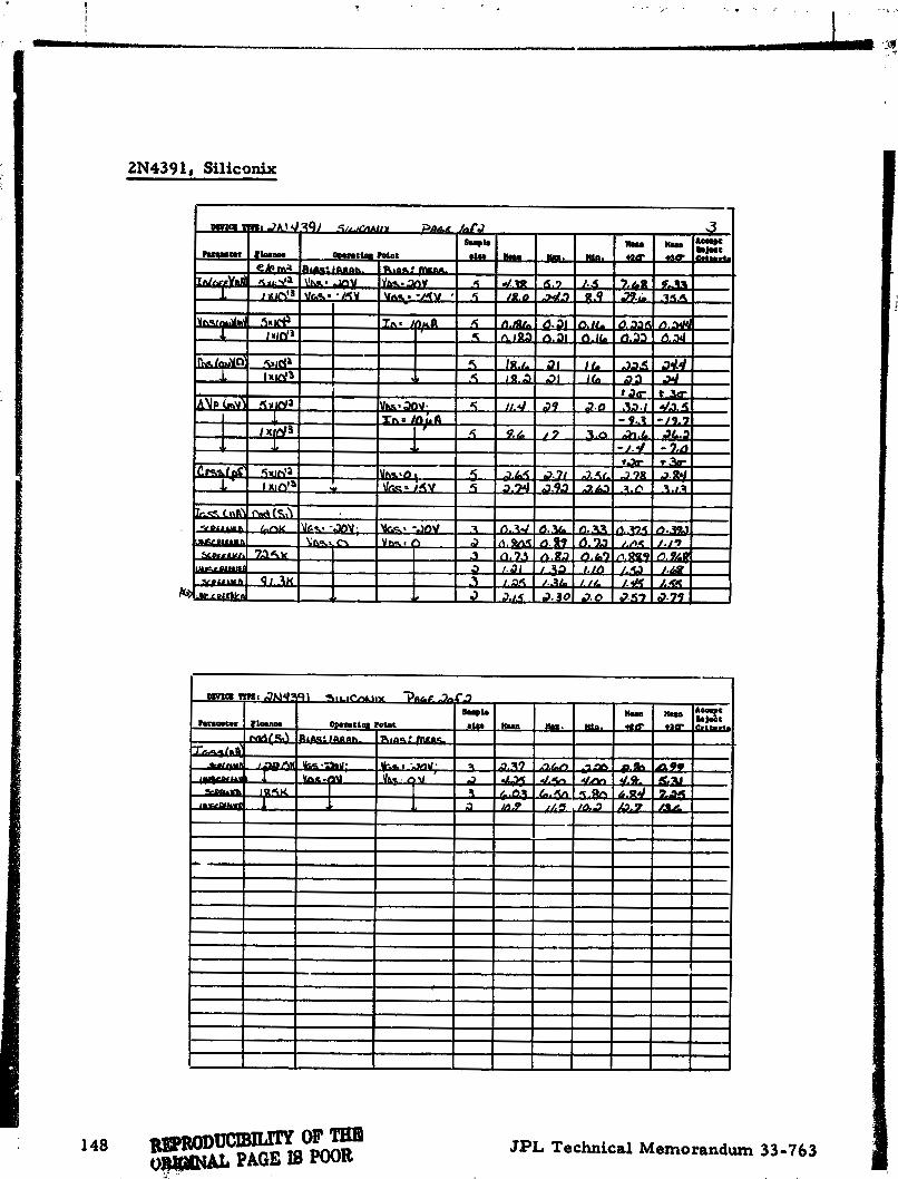
2N439 1, Siliconix
148 m m m OF 0- , a . PAGE I8
JPL Technical Memorandum 33-763
, .,,.

2N4392, Siliconix
2N43 93. Siliconix
JPL Technical Memorandum 33-763

2M4416, Siliconix
I i
2N4856, Siliconix
JPL Technical Memora~ndum 33-763

2N4856, Texas Inetruments
2N4858, Texas Inetruments
JPL Technical Memorandum 33-763

JPL Technical Mali-orandwn 33-763
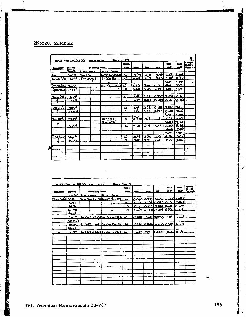
2N5520, Siliconix
JPL Technical Memorandum 33-76?
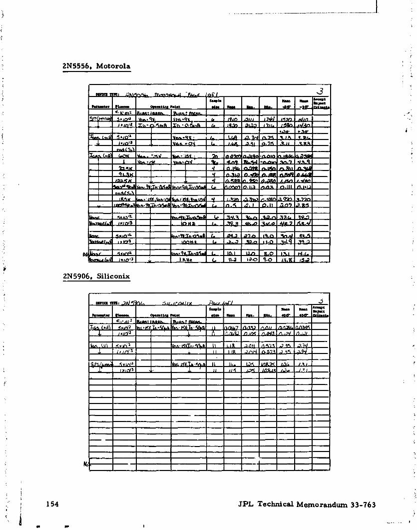
2N5556, Motorola
2N5906. Siliconix
JPL Technical Memorandum 33-76 3

JPL Technical Memorandum 33-763

C. INTEGRATED CIRCUITS
ADSSO, Analog Devices
The data presented are device linearity deltas; i. e., the effects of
LSB current changes are subtracted out of the data. For tak l esror for any
given bit, the A1 LSB must be multiplied by the bit ,tightin$ and added to the
value shown in the data. F'arameter AVBE was not stable due to servo loop
biasing and collector-base leakage current problems. Parameters AVBE
and A ( ~ / B ) are for the DUT reference transistor.
JPL Technical Memorandum 33 -763

JPL Technical Memorandum 33-763

DAC-01, Precision Monolithice
JPL Technical Memorandum 33 -76 3 i

JPL Technical Memorandum 33-763

JPL Technical Memorandum 33-763

DG129, Siliconix, IRAN reirradiation
I
DC 1 3 3, Siliconix

B~~RODUCIBILITY OF THE O u a A L PAGE IS PcnP JPL Technical Memorandum 3:-763

DG133, Siliconix, IRAN reirradiation
JPL Technical Memorandum 33-763

DG 14 1 , Silicenix
JPL Technical Mer~lorandum 33-76 3

DG 141, Siliconix, IRAN reir radiation
DG181. Intersil
JPL Technical Memorandum 33-763

DG 1 8 1, Siliconix
I _^ -- - _ ---- Arn?'.'Li~.? .?I .- -- u + - . 1 . 'L --
1 - 7
m i -
JPL Technical Memo randurn 3 3-76 3

! 1 JPL Technical Memorandum 33-763
:

JPL Technical Memorandum 33-763

I JPL 'Lechnical Mernorandrlm 33-763
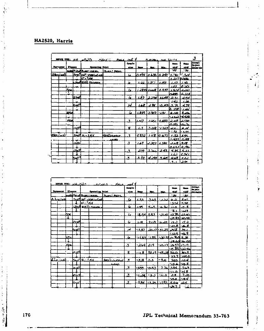
HA2520, Harris
170 JPL Technical Memo andurn 33 -76 3

JPL Technical Memorandum 33-76 3
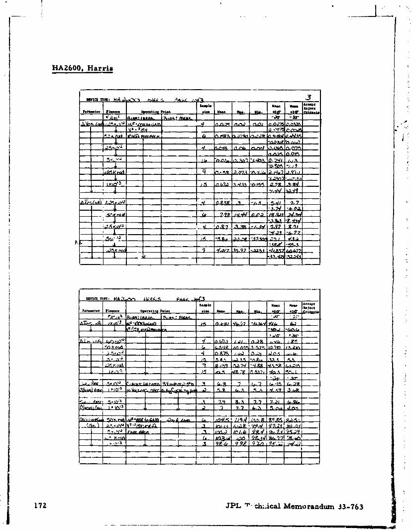
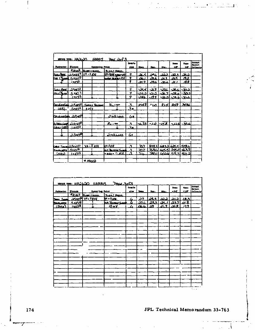
HA2600, Harris
JPL v - chi-ical Memorandum 33-76 3

HA2620. Harr i s
JPL Technica I Memorandum 33-763
JPL Technical Memo randurn 33-763

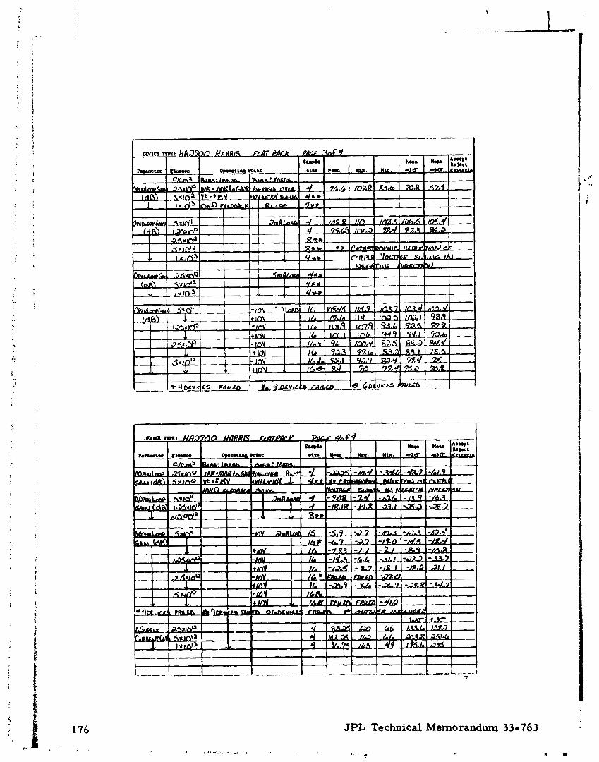
HA2700, Harrie, Flatpack
JPL Technical Mem~randurn 33-763
JPL Technical Memorandum 33-76 3
7 . . f, C .

HA2700. Harris. TO-98 f DIP
JPL Technical Memorandum 33-763

JPL Technical Memo randurn 33-7 63

ICLSOOS, Inter a i l
JPL Technical Memorandum 33-763

JPI, Technical ketnorandunl 33-763 h q
d
* ....
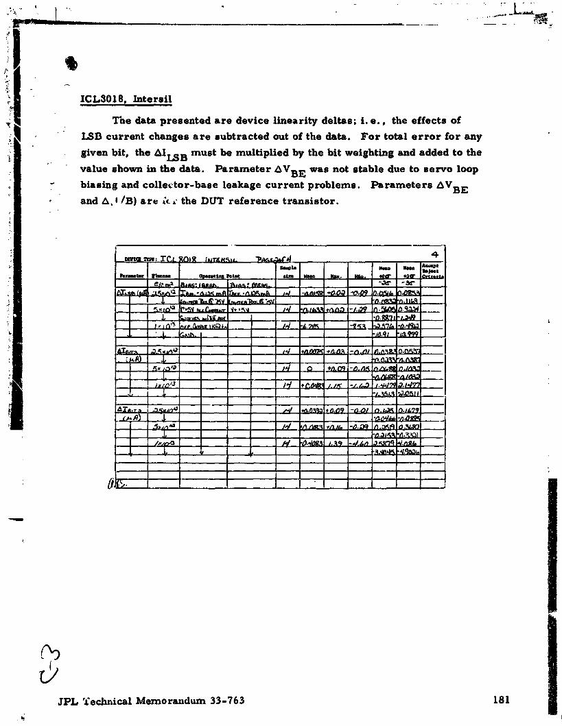
ICLSQ18, Intersil
The d a b presented are device linearity deltas; i. e., the effects of
LSD current changes are subtracted out of the data. For total error for m y
given bit. the AIuB mu& be multiplied by the bit weighting uld added to the .. .
value shown in the data. Parameter AVBE was not stable due to servo loop
- biasing and collei. tor-base leakage current problems. Rrameters AVBE a and A, 4 /B) are ir i- the DUT reference transistor.
JPL Technical Memorandum 33-763

JPL Technical Memo randutn 33-76 3

JPL Technical Memorandum 33-763

LM10 1, National Semiconductor
JPL Technical M e m o randm 33-76 3


LM10 1, National Semiconductor, IRAN reirradiation
I JPL Technical Memorandum 33-763
I

LA4 102, National Semiconductor, unhardened
LM102, National Semiconductor, hardened
JPL Technical Memo randurn 33-763

LM103, National Semiconductor
LM 105, National Semiconductor, unhardened
JPL Technical Memorandum 33-76 3

LM 105, National Semiconductor, hardened
LM106, National Semiconductor
JPL T e h i c a l Memorandum 33-763 ,-

LM108, National Semiconductor, unhardened
190 JPL Technics Memo randurn 33-763
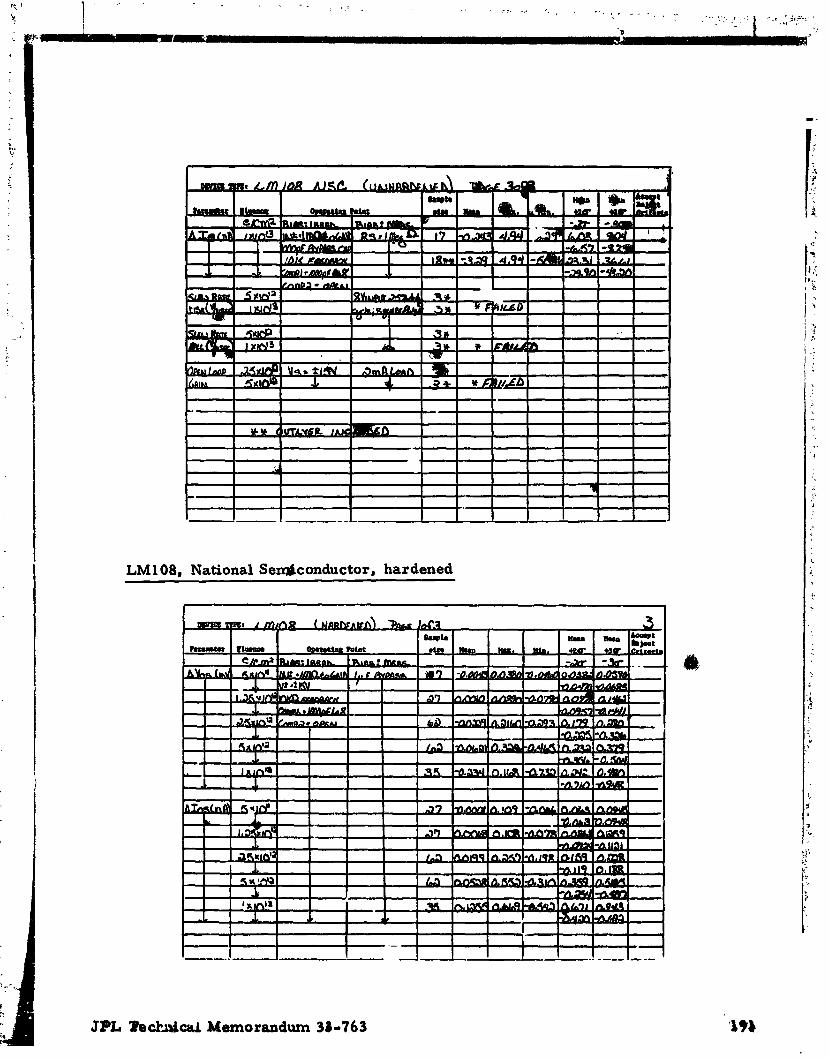
LM108, National Sedconductor, hardened

~ B C B I L r n OF THE OR!i@Olbt PAGE 18 POOR ISL Technical Memorandum 33-763

LM111, National Semiconductor, unhardened
@L Technical @emorcmdbrn 33-763

t-- . + ' ' ! . ' *
. . ._ 1
I " , - T
b . .
I .$i,
-: 7-
LQdl 1 1. National Semicanductor. IRAN reirradiation
LM 124, National Semiconductor, unhardened
JPL Technical Memorandum 33-76 3

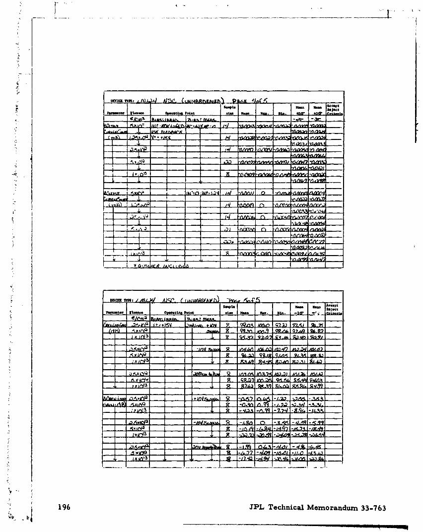
JPL Technical Memorandum 33-763
- 1 -4

LMl24, National Semiconductor, hardened
k
JPL Technical Memorandum 33-763

LM13Y. National, Signetice. and Texas Instrumente
The data presented herein represents eight radiation tests for various
vendors and date codes using different bias and measurement conditions. In
all c ~ s e s , two sections (of the faur-section device type) were tested. Device
fai. \.re is defined as saturation of the null amplifier during dc measurements;
i. e . , the device output is latched to the positive supply voltage. Table 3 i s
ir summary of the number of failures versus fluence for the various experi-
mental conditions and device lots.
National Semiconductor made various attempts to harden the LM139
with mly partial success. Several radiation tests were performed on these
expezimental devices, but only one lot (E2035, tested 11-25-75) was avail-
able for flight use and consequently included herein.
JPL Technical Memorandum 33-763 1
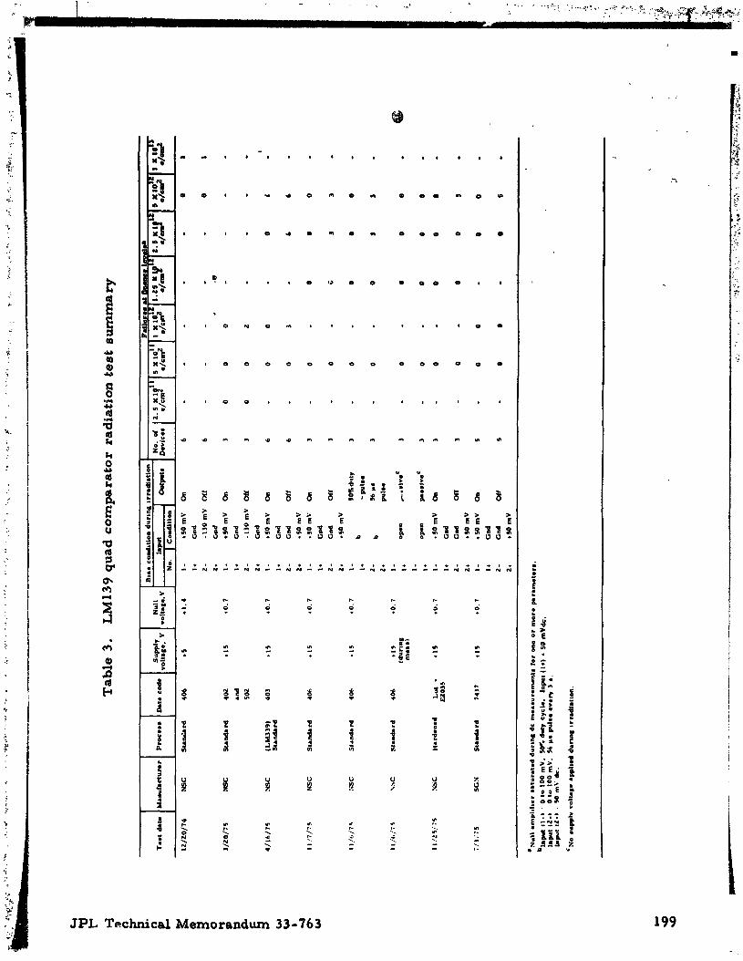
Tab
le 3
. M
I3
9 q
uad
co
mp
ara
tor
rad
iati
on
test
su
mm
ary
3/1
0/7
5
IY3C
S
Laa
d.r
d
402
and
502
4/l
h/7
5
NSC
(LM
33
9)
403
Sta
nd
ard
11
/7/7
5
NSC
Sta
nd
ard
406
.IS
to
. 7
11
5
to. 7
ld
urr
ns
mm
aml
t50
mV
O
n
Gnd
- I30
mV
O
II
Gad
tWm
V
On
Gnd
-13
Om
V
Off
God
+S
O m
V
On
Gnd
God
off
1
50
mV
-50
mV
O
o
Gnd
Gnd
Off
t50 m
V
SO
%d.
tl*
b
-pule
.
b
% C
. pl
..
I-
t+
0- ps.
iv.=
3
0
0
0
0
1/
55
NSC
Har
den
ed
LM .
11
5
10
.7
I-
e5
0m
V
On
3 0
0
0
0
U0
35
1
1
Gnd
1-
Gnd
off
3
o o
e 3
It
+W
mV
7
/3/7
5
SG
X
Sta
nd
ard
7437
t15
+O
. 7
I-
15
0 m
V
On
5
0
0
0
0
It
Gld
I C
nd
Off
5
0
0
0
5 2,
tW
mV
'nu
ll
am
pla
frcr
sa
tura
td d
urs
ns dc m
cam
ur.m
ontm
lo
r one o
r m
ore
pra
met.
ra.
bln
pl)
11-1
- 0
to
100 m
V.
50'.
duty
cy
cle.
la
pt (
It)
5
0 m
Vdc.
In
put
12-1
0
to
100 m
V.
% p
s p
d8m
o
r.^ 3
m.
Lnp
ut 1
8.)
- 50
mV
dc.

JPL Technical Memorandum 33-763
. - . --. . - .'# f
Conclusions reached were a s follows:
(1) The LA41 39 type device is ve sensitive to radiation damage. & (2) The devices biased "offH during radiation a r e more censitive to
degradation than devices biased "on" during irradiation.
(3) Device degradation may vary significantly between different date
cedes.
(4) The degradation for the devices pulsed a t 50% duty cycle is
comparable to the devices biased "onH during radiation.
(5) The degradation for the devices pulsed a t 56y sec every 3 sec
is comparable to the devices biased "off" during irradiation.
( 6 ) The parameter degrMation of the devices irradiated passively
was slightly worse $an the devices biased "onv during irradiation.
(7) The hardened National Semiconductor devices, using the same
bias conditions, did not fail until 5 X 10¹² e/cm2, whereas the
standard devices failed at 2.5 X 10¹² e/crn2. The hardened
devices showed significantly greater degrad~uon in sink current
than the unhardened devices.
(8) The low failure rate for the 12/20/74 test was due to use of
a supply voltage of 5 instead of 15 volts.

LM139, National Semiconductor, unhardened
Id- - .I -- -3- - 0
JPL Technical Memorandum 33-763
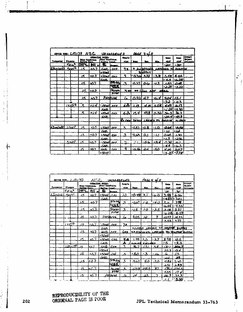
JPL Technical Memorandum 33-7 6 3

JPL Technical Memorandum 33-763
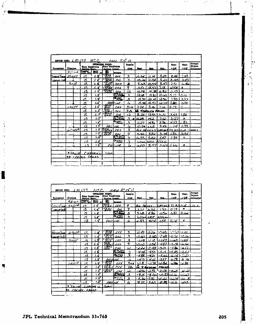
JPL Technical Memorandum 33-763

LM 139. National Selniconductor, hardened
JPL Technic= Memorandum 33-763

JPL Technical Memorandum 33-763

LM 139, Signetice
JRL Technical Memorandum 33-763
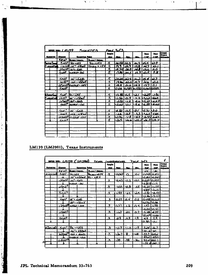
LM139 (LM2901). Texas Instrument8
JPL Technical Memorandum 33-763
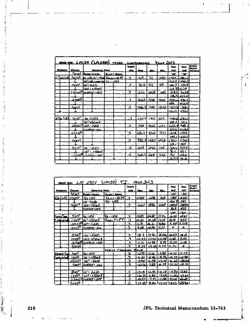
j
JPL Technical Memorandum 33-763 i

LM9 10. Nat5onal Semiconductor
JPL Technical Memorandum 33-763

LM723, National Semiconductor
BEPRODUCIBILITY OF THE F Tf'W*t PAP- TQ Wqn
JPL Technical Memorandum 33-763

MIC236, Motorola
MIC336, Motorola

D. ZENER DIODES
The radiation analysis ca r r ied out by General Electric largely f r o m
neutron data indicated potential shifts in Zener voltage sufficient to cause
problems in some applications. Electron irradiation at 2.2 MeV caused 2 relatively minor shifts in the Zener voltage a t fluences up to 1 X 10¹³ e / c m .
Additional measurements were therefore car r ied out with 3 and 5.5 MeV
electrons using the high voltage VandeGraaff a t Notre Dame University.
The Zener voltage was determined both before and af ter radiation at a
fixed current level by means of in situ measurements. This made it possible
to determine the radiation-induced change in the Zener voltage to an
accuracy of *1 mV by relatively simple means. The experiment lasted less
than one half hour and the radiation-induced thermal heating is not signifi-
cant, s o that thermal changes during the t ime of the experiment may be
ignored. The absolute value of the Zener voltage, which i s a strong function
of the Zener current, has been determined to an accuracy of about ~ 1 0 mV.
The results of the measurements a r e summarized in Table 4. It may
be noted that the majority of the devices tested do not change by more than 2 the experimental e r r o r a t a fluence of 5 X 10¹² e / c m for a l l energies up to
5.5 MeV. Three device types showed a significant linear change in Zener
voltage with electron energy, a s shown in Fig. 2. One of the device types
indicated a positive voltage shift, w h ~ r e a s the other two indicated a negative
voltage shift. These changes a r e attributed to bulk radiation damage.
Some devices of the 1N829 showed changes a s great a s 12 mV, whereas
the remainder stayed within *l mV. The anomalously large changes were not
energy-dependent, and a r e therefore considered to be due to a surface
ionization effect.
Very few of the Unitrode U28770 and U28775 high voltage Zener diodes
were available fo r testing, and these showed shifts f rom -14 to -120 mV.
The 14-mV value i s within experimental e r r o r . In cases where very few
devices were available, devices were f i r s t irradiated to a fluence of
1 X 10¹³ e/crn at 2.2 MeV and then reirradiated a t a la ter data with 3.0
JPL Technical Memo r a ~ d u m 33-763 i ,?
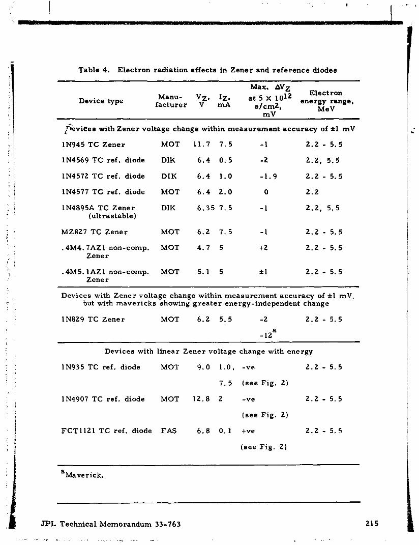
Table 4. Electron radiation effects in Zener and reference diodes
Max, AVZ Electron
Device type Manu- VZ, 12, fac ture r V rnA at 5 10" energy range,
e/cm2, MeV m V
.&vikes with Zener voltage change within measurement accuracy of t l mV *.
1N945 TC Zener MOT 11.7 7 .5 - 1 2.2 - 5.5
1N4569 TC ref. diode DIK 6 .4 0 . 5 - 2 2.2, 5.5
IN4572 TC ref. diode DIK 6 .4 1 .0 2 .2 - 5.5 I -1.9 i
IN4577 TC ref. diode MOT 6 . 4 2 .0 0 2.2 I 1N4895A TC Zener DIK 6.35 7 . 5 - 1 2.2, 5.5
(ult rastable)
MZ827 TC Zener MOT 6.2 7 . 5 - 1 2.2 - 5.5
.4M4.7AZ1 non-comp. MOT 4 .7 5 t2 2.2 - 5 .5 Zener
.4M5.1AZl non-comp. MOT 5.1 5 * 1 2.2 - 5.5 Zener
Devices with Zener voltage change within measurement accuracy of *1 mV, but with mavericks showing g rea t e r energy-independent change
1N829 TC Zener MOT 6.2 5 .5 -2 2.2 - 5.5
Devices with l inear Zener voltage change with energy I
IN93 5 TC ref. diode MOT 9.0 1.0, -ve 2 .2 - 5 .5 i I
1 N4907 TC ref. diode MOT 12.8 2 - ve 2 .2 - 5.5 1 I
( s e e Fig. 2)
FCT 1 12 1 TC ref. diode FAS 6 .8 0. i t v e 2.2 - 5.5 i ( s e e Fig. 2 ) I
-
a Maverick.
JPL Technical Memorandum 33-763 21 5

Table 4 (contd)
Max. AVZ Manu- a t 5 ~ 1 0 l ~ Electron
Device type e / cm2, energy range, facturer
mV MeV
Devices with significant Zener voltage change measured only a t 2.2 MeV
IN4581 TC ref. diode DIK 6.6 4.0 - 4 2.2
IN4891 TC ref. diode DIK 6.4 2 . 0 s - 12 2.2 (ultrastable)
7 .5 - 8
High surge non-compensated Zeners
UZ8770 UTR 70 0.05 t i 4 2.2
o r 5.5 MeV electrons. No conclusions could be drawn from the data obtained
from the second irradiation, primarily because most of the Zener voltage
shifts were within experimental e r ro r .
An attempt was made to measure changes in the temperature coefficient
of the temperature-compensated (TC) Zener diodes produced by a fluence of
1 x 10¹³ e/cm2 at energies of 2.2, 3 .0 and 5.5 MeV. These measurements
could not be carried out in situ and were therefore subject to many system-
atic e r ro r s . The main conclusion is that the pre- i r radiation temperature
coefficient of different devices of one type varies within one order of magni-
tude, whereas the radiation-induced changes a r e less than 50% of the initial
value. The temperature coefficient from -50 to t25"C decreases with
radiation, whereas the temperature coefficient from 25°C to 75°C increases
with radiation. No correlation with electron energy could be detected.
JPL Technical Memorandum 33-763

ENERGY. MeV
Fig. 2. Zener voltage change with energy
JPL Technical hlemorandum 33-763

.4M4.7AZ 1, Motorola
.4M5.1AZ 1. Motorola
JPLl Technical Memorandum 33-763

1N829, Motorola
1N935, Motorola
@ ' -
JPL Technical Memorandum 33-763

1N945, Motorola
I I I I I 1 1 I I I I I --
I l l I I I I I I
JPL Technical Memorandum 33-76 3
"F - c

1N4572, Diekson
1 ~'i577, Motorola
JPL Technical Memorandum 33-763

222 JPL Technical Memorandum 33-763
--. 7-..-- - I. I

1N4895. Dickson
1N4907, Motorola
JPL Technical Menlorandurn 33-763

FCT 1 12 1 , Fairchild Semiconductor
1 1
LVA3100. TRW
JPL Technical Memorandum 33-763
. -..---- - - - a

M2827, Motorola
I I I ! I I I I I I I
1 I I I l l
I I
U28770, Unitrode
JPL Technical Memorandum 33-763
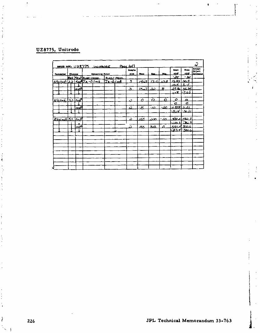
U28775, Unitrode
JPL Technical Memorandum 33-76 3

E. CONSTAKT CURRENT DIODES
1N5288, Motorola
1N5290, Motorola
JPL Technical M e m o randurn 3 3-76 3

1N5297, Motorola
1N5300, Motorola
JPL Technical Memorandum 33-763

DIODES AND RECTIFIERS
IN571 1, Hewlett-Packard
1
JPL Technical Memorandum 33-763

BC997, Texas Instruments
FJT 1 100, Fairchild Semiconductor
JPL Technical Memorandum 33-763
--- I

MV1404, Motorola
UTR4320, Unitrode
JPL Technical Memorandum 33-763

2N1878, Unitrode
2 32 JPL Technical Memorandum 33-76 3
---- ".. - - --- --. - . -
G . CAPACITORS
B 1 lB, Component Research, Teflon capacitors
JPL Technical Memorandum 33-763
. -

H . RESISTORS
CDP16-01-103G. Dale Electronics
CDP16-01-104G, Dale Electronics
JPL Technical Memorandum 33-763

CDPlb-01-223J, Dale Electronics
CDP16-01-563J. Dale Electronics
JPL Technical Memorandum 33-763

CDP16-01-6835. Dale Electronico
CDP18-02-393K, Dale Electronics
JPL Technical Memorandum 33-763

LDP16-01-153G. Dale Electronics
SDP16-02-473J, Dale Electronics
JPL Technical Memorandum 33-763

MG720, Caddock Electronics
MG750, Caddock Electronics
JPL Technical Memorandum 33-76 3

MMl 25, Caddoclc Electronics
MS176, Caddock Electronics
JPL Technical Memorandum 33-763

I. OPTICAL DEVICES
The Texas Instruments Types TIL23 and TIL24 light sources and types
TIL601 and LS600 light detectors were evaluated in the J P L Dynamitron
using a 2. 5-MeV electron beam. Two of the tests used a 0.32-cm (1/8-in. )
spacing between the source and detector in order to evaluate the spacecraft
usage conditions. Three tests used a spacing of 20 c m (8 in. ) in order to
allow shielding and consequently evaluation of the source o r detector separ-
ately. I r addition, various angles were used during irradiation in order to
reduce the amount of shielding caused by the lens material. All of the
zevices were measured in situ, within a period of 5 minutes, with the beam
off.
1. Tests Using 0.32-cm (1/8-in. ) Space
Test results using a 0.32-cm (1/8-in.) space between the light source
and detector with both device types irradiated a t the same time unshielded
were a s follows!
Test No. 1. Four TIL23 light sources acd {our LS600 light detectors
were tested on April 15-29, 1975. The test circui' i s shown below:
TIW 6 SOURCE
Due to the close spacing between the TIL23 source and LS600 detector and
the presence of the glass window, there i s an undetermined amount of
shielding of the device from the electron beam. Consequently, exposures at
a number of incidence angles for the electron beam were used ( i . e . , 45, 90,
and 135"). a s shown below, during the test.
I ' 135' BEAM
JPL Techilical Memorandum 33-76 3

C u r r e n t n ~ r a s u r d a t point@ )rA ( 9 - fluence. e,'rrn5; 6 = flux. e / c m 2 8 ) Beam
Dtbvice Date. I2 I2 I2
Angle. 1975 .L' ( p z o C D . l X I 0 , .." 9 - 2 . 5 ~ 1 0 0 ~ 5 x 1 0
bvWo 4 = 2 . 5 1 109 deg + = 0 + = I 109
- 6 = 1 . 5 109
I2 3 50 213 - 39 I20 -66 55 -84 45 4 -15
I 470 390 -17 320 - 32 2 34 -50 135 4-16
L 282 205 -27 I34 - 53 7 5 -73 45 4-16
3 0 0 213 -28 0. 36a a 19 -68 90 4-29
--
' ~ a t a invalld: the dv\ ice accidentally pulled out of position during i r rad ia t lon .
Test No. 2. Four LS600 light detectors and four TIL24 light sources
were exposed on January 22, 1975, to the electron beam at a 60" angle
(see Fig. 3). The fluence was 5 X 10'' and 1 X 10¹³ e/cm2 with a flux rate 0 2
of 2.5 X 10 ' e/cm /s. There was no significant change in the output level
a s measured a t point @ for any of the devices tested. Although the test
devices were undoubtedly severely degraded (as indicated from previous test
experience), there was still sufficient pulsed output after radiation exposure
to trigger the 2N2222A transistor "on, " therefore maintaining a constant
output a t point @. The test circuit is shown below:
CIRCUIT 1 f
JPL Technical Memorandum 33-763
PULSE AT @, CIRCUIT 1
TlU4 LIGHT SOURCE
CIRCUIT 2

2. Tes t s Using 20-cm (8-in.) Space
Test resul ts using 20 cm (8 inch) of spacing between the light source and
detector with one of the device types shielded during irradiat ion were a s
follows :
Tes t No. 1. Four TIL23 light sources were exposed t o the e lec t ron
beam a t an angle of 45 deg as shown in Fig. 4 with the detector shielded. The
t es t circuit is shown below:
Tes t No. 2. Fou r TIL6Ol light detectors were exposed on January 22,
1975, to the electron beam a t a 45-deg angle a s shown in Fig. 4 with the
light source shielded. The te3t circuit i s shown below:
Device S/N
5
6
7
8
LIGHT SOUPCE
JPL Technical Memo randurn 33-76 3
A, %
-98.3
-98.3
-96.4
-98.0
TIL23 output voltage measured a t point @ m V
( a = fluence, e/crn2; + = flux, e/cm2/s)
@ = 0 + = 0
0.240
0.360
0.140
1.900
@ = 5 ~ 1 0 12 + = 3.6 x lo9
0.014
0.022
0.014
0.116
a, %
-94.2
-94.0
-90.0
-94.0
i9= 1 ~ 1 0 13 9 = 3.6 X 10'9
0.004
0.006
0.005
0.038

TIL601 cur ren t measured a t point @, nA ( o = fluence, e/cm2; + = flux, e/cm2/s)
Device S/N a = o @ = 5 x 10¹² a = 1 1013
4 = 0 + = 3.6 x 10⁹ A" 0 = 3.6 x 10¹⁹ A,+
1 250.0 129.0 -48.4 38.0 -85.0
2 96.0 19.2 -80.0 8.0 -91.7
3 160.0 65.0 -59.4 19.0 -88.1
4 112.0 78.0 -30.4 53.0 -52.7 i
i I
Tes t No. 3. Four TIL24 light sources were exposed to the electron
beam a t an angle of 45 deg a s shown in Fig. 4 with the detector shielded.
The tes t circuit i s shown below:
SHEU)ED PHOTO TRANSISTOR
MEASUREMENT POlM
2 k Q , 1%
A , '70
-95.3
-98.6
-97.7
Device S/N
- 1
2
9
10
TIL24 voltage measurement a t point 9 mv ( 0 = fluence, e/cm2; $ = flux, e/cm / s )
= 1 1013 $ = 3.6 X 10⁹
0.015
0.003
0.009
0.016 -99.5
A , %
-85.2
-95.4
-92.2
. a = o + = 0
0.318
0.218
0.384
-93.1
0 = 5 x 10¹² + = 3.6 x 10⁹
0.047
0.010
0.030
3.000 0.208

3. Conclusions
(1) These types of optical devices a r e ve ry sens i t ive to radiation-
induced damage.
(2) The light sources a r e m o r e sensi t ive to radiation damage than the
detec tors .
( 3 ) T h e r e i s inc reased light s c a t t e r due t o the degraded s o u r c e lens .
(4) T h e r e i s m o r e apparent degradation with 20-cm (8- in . ) spacing
between the source and detec tor than with 0.32-cm (1/8-in.)
spacing because the light f r o m the source d e c r e a s e s a s the
square of the distance f r o m the detector , and any i n c r e a s e in
light sca t t e r will exhibit m o r e effect a s the d is tance i s increased.
4. Tes t Conditions
The device shown in Fig . 3 was i r radia ted with the axis of the e lec t ron
beam a t 60 deg t o the axis of the device a s shown in the d iagram in o r d e r t o
avoid the g lass lid.
h 1 ~ 4 (UMHIELDED)
APPROXIMATELY 0.32 cm (1/8 in.)
LS600 (UNSHIELDED) 0 Fig . 3 . Flux angle, e lec t ron beam a t 60 deg
No other components of the experiment were changed. A cosine va r i a -
tion in fluence with incident angle was used. The Faraday cup readings of 2 fluence were thus twice the fluence required ( i . e . , 1013 and 2 X 10¹³ e /cm ).
The effective vaicle of the fluence on the device was obtained a s of these 2 values ( i . e . , 5 X 10 l2 and 1":' e / cm . This was done by vsing a t ime
exposure twice a s long ra the r than doubling the flux ra te . Thus the effective
flux ra te a t the device was one-half that in the tes t requi rements .
JPL Technical Memorandum 33-763
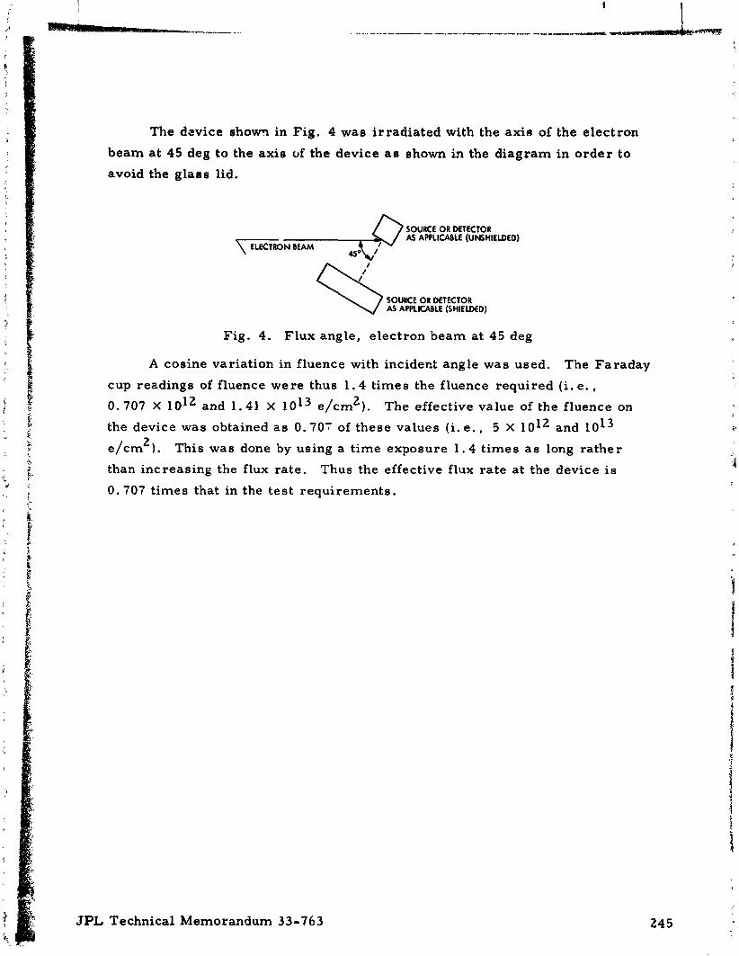
The davice shorn in Fig. 4 was irradiated with the axir, of the electron
beam a t 45 deg to the axie of the device a e shown in the diagram in order to
avoid the glae s lid.
SOURCE OR DETECTOR AS APPLICABLE (UNSHIEU>ED)
\ON BEAM
SOURCE OR DETECTOR AS APPLICABLE (SHIELDED)
Fig. 4, Flux angle, electron beam at 45 deg
A cosine variation in fluence with incident angle was used. The Faraday
cup readings of fluence were thus 1.4 times the fluence required ( i . e. , 0.707 X 10¹² and 1.41 X l o i3 e/crn2). The effective value of the fluence on
the device was obtained a s 0.707 of these values (i. e . , 5 X 10¹² and lo i3 2 e/cm ). This was done by using a time exposure 1 .4 times a s long rather
than increasing the flux rate. Thus the effective flux rate at the device i s
0.707 times that in the test requirements.
P JPL Technical Memorandum 33-763 C

J. CMOS
Large quantities of CMOS devices comprising 28 different logic func-
tions a r e used in the spacecraft. Devices fabricated by the standard
commercial process could not withstand a dose of 150 krad(Si) under normal
bias conditions due to shift of the n-channel gate turn-on voltage toward 0 V
accompanied by a large increase in the supply current. By reducing the gate
oxide annealing temperature (Ref. 2 ) it was found possible to fabricate
devices that were still functional af ter irradiation to 150 krad(Si) though
somewhat degraded in the device characterist ics . A program was developed
to monitor the radiation properties of the production line that included wafer
lot sampling of changes in the quiescent supply current, test pattern sampling,
and final device parameter characterization. All irradiations were carr ied
out under representative usage bias conditions using a cobalt-60 source.
The four basic CMOS failure modes in an ionizing rddiatior environ-
ment have been identified by Burghard and Gwyn (Refs. 3 and 4) with their
associated causes a s follows:
(1) Failure to switch - (2) Excessive leakage - lVTnl I (3) Speed rc '-lction - I V ~ ~ I t (4) Noise immunity -
T I'TPI 1 The arrows indicate a decrease o r increase in V , 1 7 1
1 . Gate Turn-on Voltage
Three to five test pattern dice were selected a t random from each
metallization lot. The test pattern dice contain individual N- and P-channel
t ransis tors and MOS capacitors. Measurement of I versus VGS of the DS 5 two t ransis tors was made before and a f te . a dose of 1.15 X 10 rad(Si). A
typical set of curves i s shown in Fig. 5. The results for the N-channel
transistor a r e particularly striking. The true gate turn-on voltage V Tn
at low currents i s less than 1 1' before irradiation and shifts to -0 .6 V at
150 krad. At higher current levels V T n stays well above zero, a s shown
in Fig. 6 , and does not shift significantly after irradiation ( see Fig. 7 ) .
JPL Technical Memorandum 33-763
- . 1 1 1 1 1 1 - - . 1 1 . 1 - . 7 - -111111 1 - b. . . . . . . - t

Fig. 5. 1V- and P-channel gate drive transfer characteristics
JPL Technical Memorandum 33-743

190 DEVICES FROM 70-80 LOTS A
0 O.? 0.4 0.6 0 .8 1.0 1.2 1.4 1.6 1.8 2.0 2.2 2.4 2.6 2 .8 3.0
PREWADIATION, . V,,,
Fig. 6 . Threshold voltage of N-channel transistor on t e s t pattern TA 6372, 950°C gate oxide anneal in <arming g a s , preradiation
Fig. 7 . Threshold voltage of N-channel transistor on test pattern TA 6 3 7 2 , 950°C gate oxide anneal in forming gas, postradiation
JP1, Technical Memorandum 33-763

On the other hand, V T p a t 10 pA shows a bimodal distribution af ter rrradia-
tion,which may explain the lack of control of the propagation time (see
Figs. 8 and 9). The distribution in the relative shift in the gate turn-on
voltages i s shown in Fik. 10.
The gate turn-on voltage is the most direct way of radiation-screening
CMOS devices. However, the approach adopted in the MJS project was to
monitor the quiescent supply current, which i s related to VTn a t low
currents but does not control V TP'
Mareover, there i s no correlation in
the behavior of these two parameters , since V a t 150 krad(Si) i s Tn primarily a function of radiatiot- induced oxide states, whereas V i s a
T P function of radiation-induced interface states.
The gate turn-on voltage V i s the parameter directly affr ced by T ionizing radiation. The V i s , however, a t ransis tor p a r a m e ~ d r , not a T circuit parameter. The transfer characterist ics of any Cx40S circuit allow
considerable shift in V o r V before the circuit runctioll ceases. The Tm TP
'prn1 may even cross 0 V and be slightly negative before functiona! failure
occurs.
PHERADIAT'ON, - VT,
Fig. 8. Threshold voltage of P-channel t ransis tor 011
tes t pattern TA 6372, 950°C gate oxide anneal in forming gas, pre radia tion
JPL Technical Memorandum 33-763

188 DEVICES
. . 1.4 1.6 1.8 2.0 2.7 2.4 2.6 2.8 3.0 3.2 3.4 3.6 3.8
POSTRADIAIION, 1 . I 5 . lo5 rod, - VTn
Fig. 9. Threshold voltage of P-channel transistor oc test pattern TA 6372, 950" C g ~ t e oxide anneal in forming gas, postradiation
I I I I I I I I I I I I I I I I I I I I I I I I I I I I 0 .4 0.2 0 -0.2 -0.4 -0.6 -0.8 -1.0 -0.2 -0.4 -0.6 -0 .8 -1.0 -1.2 -1.5 -2.3
v v AN-CH VGS AT IDS 10 p A AP-CH VCS AT IL -10 FA
N-CHANNEL P-CHANt.CL
Fig. 10. Distribution of A'dGS at IDS after 1 . 5 x 10¹⁵ rad(Si)
JPL Technical Memo randurn 33-763

2. Wafer Screening of ISS
JPL Technical Memorandum 33-763
Wafer screening consisted of irradiating five circuit devices o r seven
in the case of the three multiplexers f rom each wafer that would be used for
the JPL product. The quiescent supply current I was measured with a l l SS
input terminals to ground and with a l l input terminals connected to 10 V.
Rejection was based on an I measurement a f te r 150 krad(Si). The rejec- SS
tion cr i ter ia a r e given in Table 5. These cr i ter ia have considerable margin
to functional failure.
The rejection rate a t 150 krad was less than 10% for some simple
circuits (gates and flipflops) and greater for complex and large-area circuits
(counters, shift regis ters , multiplexers and buffers). More than 2700 wafers
have now been screened in this manner.
The test dice were not specially screened for I before irradiation. SS
As indicated in Fig. 11, 75% of the devices (Group 1) had leakage currents
below 1 nA, another 20% (Group 2) possessed greater leakage currents , but
sufficiently low to pass the JPL specifications, whereas the remaining 5%
(Group 3) w o ~ l d have been rejected in pre-irradiation screening. The post-
irradiation data for Group 1 (Fig. 12) shows a reasonable Gaussian dis t r i -
bution, but with the rejection limit se t so a s to cause a 12% rejection rate.
The more than 10,000-fold increase in I appears to be the best that can be SS
achieved on this type with the modified annealing process, and i s attributed
to the shift in VTn toward 0 V. Group 2, with marginal pre-irradiation
properties produced a post-irradiation yield of only 66% (see Figs. 1 3 and 14).
A preliminary study on the variation of I over a given wafer af ter SS
irradiation indicates a tight distribction in some wafers, while other wafers
exhibit a great deal of variability. This i s in agreement with the general lot
variability of the product observed during radiation screening.
The distribution of IS_ has been analvzed for a number of different
device types and for both forming gas and nitrogen annealing. The results
for the CD4052 and CD4049 a r e shown in Figs. 15 through 22. The data
indicates a nurnber of bimodal distributions caused by lack lf process
control, but that nitrogen annealing offers a substantially better product.
The data that has been analyzed in this manner i s summarized in Table 6 .

Table 5. Rejection cr i ter ia for RCA CMOS wafer radiation screening
ISS (post- radiation), p A
ISS i s quiescent supply current measured with a l l inputs low (ISS1) and a l l inputs high (ISS2).
1 i s off-leakage current through al l transmission gates (switches) in L parallel. IL1 i s measured with a l l switch inputs high (10 V ) and the switch common to ground through the current mcter. IL2 i s measured with the switch common high and all switch inputs to ground through the current meter .
JPL Tech.r.lc:.al Memorandum 3 3 - i o 3
.--... - -- ----- .ir

380 DEVICES FROM 53 WAFERS FROM 7 LOTS
10 30 1W 300 1 3 10 30 100 3 F 1 3 10 30 100 300
nA- PA rA CURRENT
Fig. 11. RCA CD4006, preradiation, ISSl
JPL Technical Memorandum 33-763

GROUP I 1 . 5 k 1 0 ~ ( u a d
300 1 3 10 SO 1 0 0 3 0 0 I 3 10 30 1 0 0 J 0 0 1 3 10
4 ~ . nA PA -&- mA - CURRENT
Fig. 12. RCA CD4006, postradiation ISSl of units with preradiation ISS~ < 1 rnA
UNITS WITH PRERADlATlON lSSl
>I nA A N D .C 300 nA (ST LIMIT)
1 REJECTION
I
GROUP 2
1 3 10 30 100 300 1 3 10 30 100 300 1 3 10
~ - A A - ~ ~ A ~ ~ A -
CURRENT
Fig. 13. RCA CD 4006, preradiation, group 2
JPL Technical Memorandum 33-763
.. . . --"-- -.- \

POSTRADIATION lSSl OF UNITS WITH
PRERADIATION ISSI > 300 nA (ST LIMIT) I I
GROUP 3
1 REJECTION
I 30pA
~--,.AA~A-- CURRENT
Fig. 14. RCA CD4006, group 3
ST LIMIT 500 n A
GROUP 2
10 3C 100 300 1 3 10 30 100 300 1 3 10 J) 100 300
.- PA -- n.4 --=- FA
CURRENT
Fig. 1 5 . Preradiation ISS current of CD4052A multi- plexers with 950" C gate oxide anneal in forming g a s
JPL Technical Memorandum 33-763

GROUP 2 t --REJECTION LIMITS 50
--REJECTION
30 100 300 I 3 10 30 100 300 1 3 10 30 100 330
P A * - . - ~ A . - = - P A
CURRENT
Fig. 16. Postradiation ISS current of CD4052A multiplex- e r s with 950°C gate oxide anneal in forming gas
10 30 100 300 1 3 10 30 100 300 1 3 10 30 100 300
pA -+-~ nA P A
CURRENT
Fig. 17 . Preradiation ISS current of CD4052A multiplex- e r s with 950°C gate oxide anneal in nitrogen
JPL Technical Memorar~dum 33-763

REJECTION LIMIT W p A
GROUP 2 1
- - p A 4 - n ~ , 1 , ~ ~
CURRENT
Fig. 18. Postradiation ISS current of CD4052A multiplexers with 950' C gate oxide anneal in nitrogen
JPL Technical Memorandum 33-763

VDD -Vss = I O V
~ A ~ ~ A - I - P A CURRENT
Fig. 19. Preradiation IS current of CD4049 with 950" C gate oxi c? e anneal in forming gas
t -- REJECTION LIMIT 7 . 5 ~ A
GROUP l
p~--4-----n*F CURRENT
Fig. 20. Postradiation ISS current of CD4049 with 950' C gate oxide anneal in formifig gae
JPL Technical Memorandum 33-763

VDD - vss I O V
Fig. 21. Preradiation ISS current of CD4049 with 950°C gate oxide anneal in nitrogen
GROUP l
PA- ~A--+A - CURRENT
Fig. 22. Postradiation ISs current of CD4049 with 950°C gate oxide anneal in nitrogen
JPL Technical Memorandum 33 - 763

Table 6. Analysis of ISS data
Annealing Peak of Other Rejection Device Function Distribution p r i m e peaks,
type gas devices P A l imi t , pA
CD4006 18-stage Forming Gauss ian 10 pA 30 shift r eg i s t e r gas
CD 401 3 Quad And-Or Forming Gauss ian 5 nA 7 . 5 gate gas
Nitrogen Gauss ian 20 nA 7 . 5
CD 4027 Dual flipflop Forming Gauss ian 20 -A 7 . 5 gas
CD 4029 up/down Forming Bimodal 50 nA 20 5 0 counter gas
Nitrogen Bimodal 5 nA 2 50 50 nA
CD 4049 Hex-buffer Forming Bimodal 50 nA 2 7 . 5 gas
Nitrogen Quasi- 20 nA 2 7 . 5 Guassian
CD 4052 Multiplexer Forming Bimodal 3 nA 2 5 0 & a s 30
Nitrogen Gauss ian 500 n A 5 0
It is evident that the rejection l imi ts do remove lots with lack of s ~ i f a c e
control . The rcjection l imi ts were choseq to s c r e e n out wafers with
catastrophic devices o r with I higher than acceptable to the projec t SS s y s t e n ~ s des igners . The yield f i g ~ ~ e s of the wafer s c r e ~ n i n g p rogram a r e
summarized in Table 7.
Inc reases in I a r e a problem for the u s e r (subsys tem des igner) only SS
wrhen the total for a subsys tem exceeds the cu r ren t avai lable f o r the power
supply, o r when the subsys tem power limitation i s exceeded. Therefore ,
i t i s the average of the inc reases that i s of in te res t , not t l ~ e i-ld'vidual
i n c r e a s e s in 1 SS ' All the R C A CMOS that will be supplied a r e f r o m wafers
whose tes t samples had a post-I50 k rad I of l e s s than 100 t imes the 25OC SS
specification l imit- S? 11868 o r MIL-STD-38510 or equivalent ( s e e Table 5) .
JPL Technical Menlorandurn 33-763
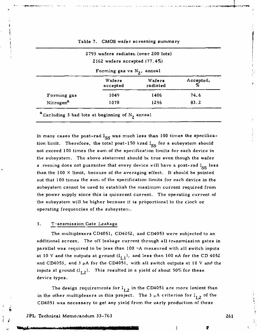
Table 7. CMOS wafer screening s u m m a r y
2793 wafers radiatecr (over 200 lots)
2 162 wafers accepted (77.4%)
Forming gas v s N2, anneal - - - -
Wafers Wafers Accepted, accepted radiated 70
Forming gas 1049 1406 74.6
a ~ x c l u d i n g 5 bad lots a t beginning of N2 anneal
In many c a s e s the pos t - rad ISS was much l e s s than 100 t imes the spacif ica-
tion l imit . Therefore , the total post- 150 krad I fo r a subsys tem should SS
not exceed 100 t imes the s u m of the specification l imi ts for each device in
the subsystem. The above s ta tement should be t rue even though the wafer
s reening does not guarantee that every device urill have a pos t - rad I l e s s SS than the 100 X l imi t , because of the averaging effect. It should be pointed
out that 100 t imes the sun, of the specification l imi ts f o r each device in the
subsys tem cannot be used to establish the maximum cur ren t required f r o m
the power supply since this i s quiescent cu r ren t . The operating cur ren t of
the subsys tem will be higher because it i s proport ional to the ciock o r
operating f r e q u e ~ c i e s of the subsys tem.
3. T .-ansmission Gate Leakage -.
The mult iplexers CD4051, CD4052, and CD4053 were subjected to an
additional sc reen . The off leakage cur ren t through a l l t rdnsmiss ion gates in
para l le l was required to be l e s s than 100 -A measured with a l l switch inputs
a t 10 V and the outputs a t ground (IL1). and l e s s than 100 nA fo r the CD 4052
and CD4053, and 3 pA for the CD4051, with a l l switch outputs a t 10 V and the
inputs a t ground (IL2). This resulted in a yield of about 50% fo r these
device types.
The design requi rements f o r i in the CD4051 a r e m o r e lenient than L2
in the o ther mult iplexers in this projec t . The 3 1.4 c r i t e r ion fo r I of the L2
CD4051 was necessa ry to get any yield f r o m the ea r ly production of these ! $.
> JPL Technical Memorandum 33-763 9
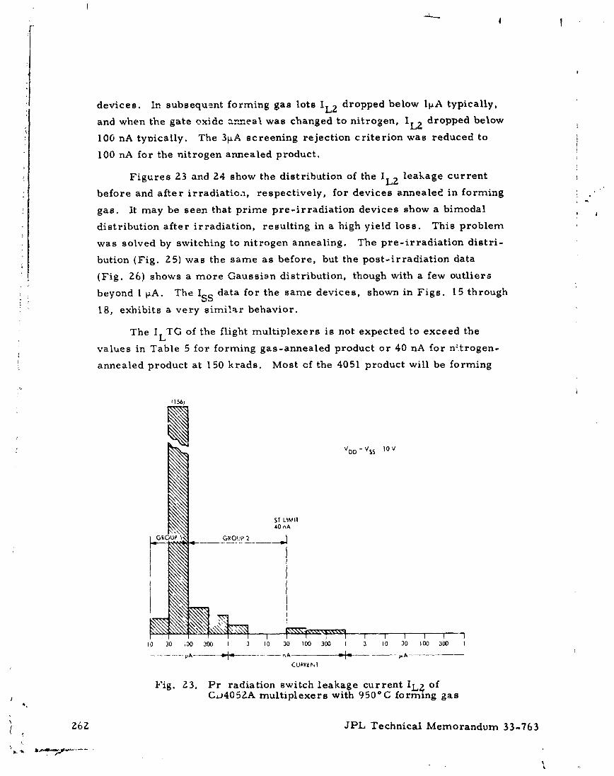
devices. In subsequ2nt forming gas lots IL2 dropped below 1pA typically,
and when the pate ~ x i d e :zzea\ was changed to nitrogen, IL2 dropped below
100 nA t y ~ i c a l l y . The 3pA screening rejection cri terion was reduced to
100 nA for the nitrogen annealed product.
Figures 23 and 24 show the distribution of the IL2 leakage current
before and after irradiatio.1, respectively, for devices annealeZ in forming
gas. It may be seen that prime pre-irradiation devices show a bimodal
distribution after irradiation, resulting in a high yield loss. This problem
was solved by switching to nitrogen annealing. The pre-irradiation dis t r i -
bution (Fig. 25) was the same a s before, but the post-irradiation data
(Fig. 26) shows a more Gaussian distribution, though with a few outliers
beyond 1 pA. The ISS data for the same devices, shown in Figs. 15 through
18, exhibits a very similar behavior.
The I TC of the flight multiplexers i s not expected to exceed the L values in Table 5 for forming gas-annealed product o r 40 nA for n'trogen-
annealed product at 150 krads. Most cf the 4051 product will be forming
VDD - VSS I O V
LIMIT n A
Fig. 23. P r radiation switch leakage current IL2 of Cd4052A multiplexers with 950' C forming gas
JPL Technical Memorandum 33-763
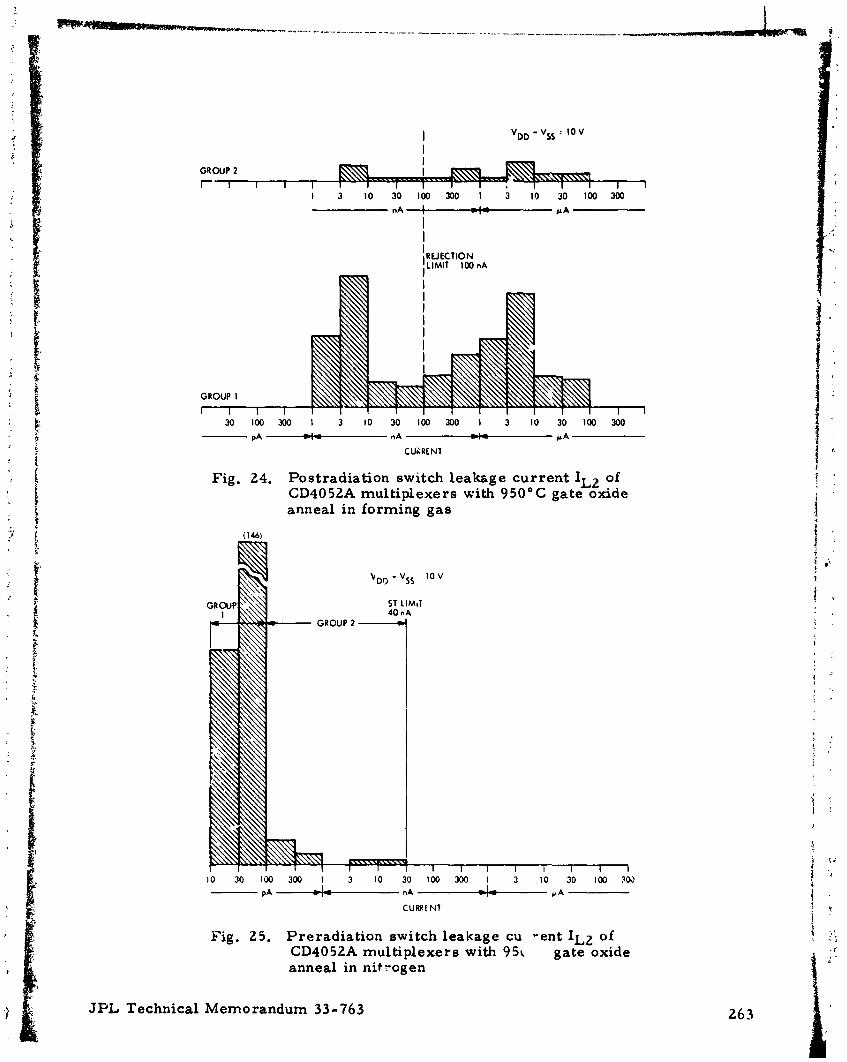
GROUP 2
r I I 1 3 10 30 100 300 1 3 I0 30 100 300
Fig. 24. Postradiation switch leakage current IL2 of CD4052A multiplexers with 950" C gate oxide anneal in forming gas
\ . --,
LDD - vss IOV
ST LIMIT
GROUP 2
1 1
I 1 I I I I I 1 1 10 30 100 300 1 3 10 30 100 300 1 3 10 30 100 3W
PA --nA P A
CURRENT
Fig. 25. Preradiation switch leakage cu -ent IL2 of CD4052A multiplexers with 95i gate oxide anneal in nitrogen
JkL Technical Memorandum 33-763

VDD - VSS I O V
I GROUP 2 I
1 1 1 I 1 1 300 1 3 10 30 1W 300 1 3 10 30 100 300
- a 4 - I PA - nA , - - *A
I I
11C5) I ' REJECTION 1 LIMIT 100 n.1
I OUTLIER AT 700 m A
! l l I I I I I 1 I 13 ZJW 1 3 . J 30 100 300 1 3 13 30 100 300
- 3A - ------ n A -1- - - P A - CURRENT
Fig. 26. Postradiat ion switch leakage c u r r e n t IL2 of CD4052A mult ip lexers with 950°C gate oxide anneal in nitrogen
gas-annealed. The 4052 produc; will be a combination of forming gas - and
nitrcgen-annealed devices, and the 4053 prodxct will b e entirely
nit rogen-annealed.
4. ;.Iultiplexer Or.-Resistance
The on- res is tance of the mult iplexers inc reases l e s s than 5% a t
75 krads and 10% a t 150 krads .
5. Propagation Time
4 complete e l e c t ~ i c a l charac ter iza t ion nf some of the CMOS devices
was c a ~ r i e d out for T t J b a t the Naval Research Laboratory using an EH4600 4
sei- ies cor,~pl.~ter-controlled t e s t sys tem a t a total dose of 7 . 5 X 10 and 5
1. 5 x !I) ra3(Si). The p a r a m e t e r s tested and some typical resul t s a r e
JPL Technical biernorandurn 33-763

shown in Table 8. It may be noted that radiation causes a significant
increase in the propagation time. It was established that there i s no
correlation between the radiation effects on propagation delay and quiescent
supply current ISs
Table P . CMOS radiation characterization data a t 150 krad(Si)
Tests . (At VDD = 10 V ) 401 1 4029 4035 40 50
1. Functional (go/no go) vo < 5 v = "0" V > 5 v = "1"
0
2. DC margin (go/no go) v < l V = " O M
0 v > 9 v = "1" 0
3. At Pm ($1 Average 26. 9a
30 pF load Maximum 30
3a. At PLH (%) Average
30 pF load Maximum
4. At ~ H L (70) Average 6. 2a 30 pF load Maximum 8.8
4k. At ~ H L (Too) Average 30 pF load Maximum
All passed
All passed
5. AV drop in output t rans- N-CH<0.1 V < 0.1 <0.1 <O. 1 istr rs a t m i ~ i m u m source/ P-CH < 0.1 V < 0.1 - 0.1 <O. 1 sink current specified in RCA manual
6. Range of maximum qirie- from: 56X 2 50X 23X 2 5X scent supply current A to: 4700X 9800X 3300X '3400X
a Propagation time measurement from pin 2 to pin 3 (in to out).
i b~ropaga t ion time measurement from pin 15 to pin 6 (CL. to 01 ). C Propagation time measurement f rom pin 6 to pin 1 (CL. to Q1).
d ~ r o p a g a t i o n time measurement from pin 3 to pin 2 (in to out). !
t e Propagation time measurement from pin 15 to pin 7 (CL. to ca r ry out).
2 JPL Technical Memorandum 33-763

A more d2tailed analysis was car r ied out on additional measurements
made a t the Hughes (Fullerton) Facility ( see Table 9). The propagation t ime , * . . af te r irradiation appears to be within the J P L specification l imits, but the _ I -
data shows large increases in propagation time. These a r e primarily
influenced by outliers whose change may be up to one order of magnitude worse . .
than the mean. 1
6. Dose Rate and Anne ling Effects . .
Srour (Ref. 5) recently reviewed experimental observations on dose-
rate dependence of the shift in VT in MOS devices. The dependence i s a
' ..lction of the dose rate, the bias conditions during radiation and also the
nature of the gate oxide. Srour irradiated N- and P-channel t ransis tors on
a commercial CMOS inverter using a ~ 0 6 0 source a t rates of 0.23 and
23 rad(Si)/s. He observed a marked rate effect. Annealing the devices a t
room temperature for 140 hours (the time i t takes to perform an i r rad i t ' a ion 5
to 1.2 X 10 rads a t a rate of 0.23 rad/s) following a higher ionization rate
irradiation brought the high and low dose-rate results into agreement.
Yamakawa (Ref. 6) measured rate effects in I of CMOS devices with SS
a 950°C gate-oxide anneal temperature a t 113 and 7.6 rad/s a t a total dose of 5
1. 5 X 10 rad(Si). The bias conditions were a s described in the wafer screen.
The two dose rates represent the screening conditions and the '~ovian radia-
tion environment respectively. There was a strong annealing effect af ter
radiation, tut no rate effect could be detected. Additional experiments on the
propagation time showed no annealing for several days. in agreement with
the hypothesis that the propagation time i s governed by interface states.
7. Conclusions
The radiation resistance of CMOS devices with a gate oxide annealing
temperature of 950°C appears to be adequate for the MJS project, because
the devices will be exposed to a total dose of l ess than 1.25 x 1c5 krad and
because no severe cc ,~ \ ' ra in t s have been imposed on the quiescent supply
current.
Preliminary data indicate that the substitution of forming gas by
nitrogen in the gate oxide annealing s tep has a ve;.v beneficial effect on J
JPL Technical Memorandum 31-763
--- I r

Ta
ble
9.
Pro
pa
ga
tio
n t
ime
.a
Pro
pa
ga
tio
n t
ime
, ne
1 M
ean
Max.
-
~
--.
Ca
pa
ci-
Dev
ice
Sp
ecif
ied
P
re
- 1
.5 X
P
re
- P
ara
met
er
tan
ce C
L.
1.2
x
A M
ax
. ty
Pe
lim
it
irra
dia
te
10
5r
ad
ir
rad
iate
1
0
rad
PF

Tab
le 9
(c
on
td) Pro
pa
ga
tio
n t
ime,
ns
Mea
n
Max
Dev
ice
Ca
pa
ci-
Sp
ecif
ied
P
re
- 1
.5 X
P
re
- 1
.5 X
P
ara
met
er
tan
ce C
L,
A
Max
. ty
pe
lim
it
irra
dia
te
lo5
rad
ir
rad
iate
lo
5 r
ad
DF

reducing the post-radiation quiescent supply current and transmission gate
leakage currents of the multiplexers and on producing a more homogeneous
product.
The wafer screening of I i s expensive but necessary in view of the SS
lack of safety margin shown in the distribution, the presence of outliers and
bimodal distributions. F o r future programb, radiation screening of N-
channel and P-channel test transistors associated with each wafer should be
considered, since the absolute values of post-irradiation VTn nnd V a r e TP
more fundamental parameters directly related to oxide and interface states.
At present V is not screened, and this produces a barely tolerable TP
variation in the propagation time. In future programs other process controls
involving capacitor measurements should be considered in direct collabora-
tion with the manufacturers. Such controls have been described in a paper
by Gregory (Ref. 4).
Finally, any futc e programs with a radiation environment in excess
of that encountered by hlJS o- with more stringent design requirements must
use the radiation hard dry gate oxide process developed a t RCA, Somerville,
with DNA support, o r equivalent, since the 950°C annealed process cannot 5 survive a total dose much greater than 1. 5 X 10 rad(Si).
' 6
k - ' I '
CD4001, RCA
I I I I l . I I
JPL Technical Memorandum 33-763
. . " ---- ---.- .d
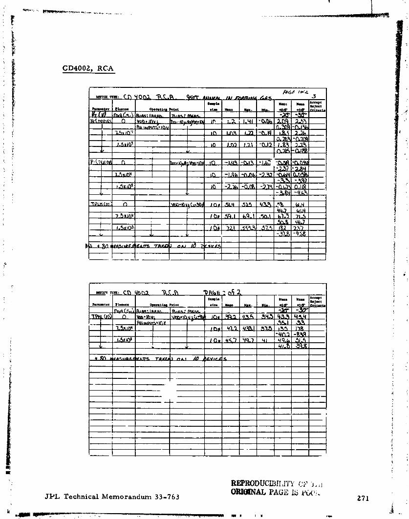
CD4002, RGA
REPRODUCIBII ,Irl'Y (:F i , , : ORIOQNAL PAGE IS p a i ! ,,
JPL Technical Memorandum 33-763

CD4006, RCA
i - i 1 1 1 -- I
JPL Technical Memorandum 33-763
rl I
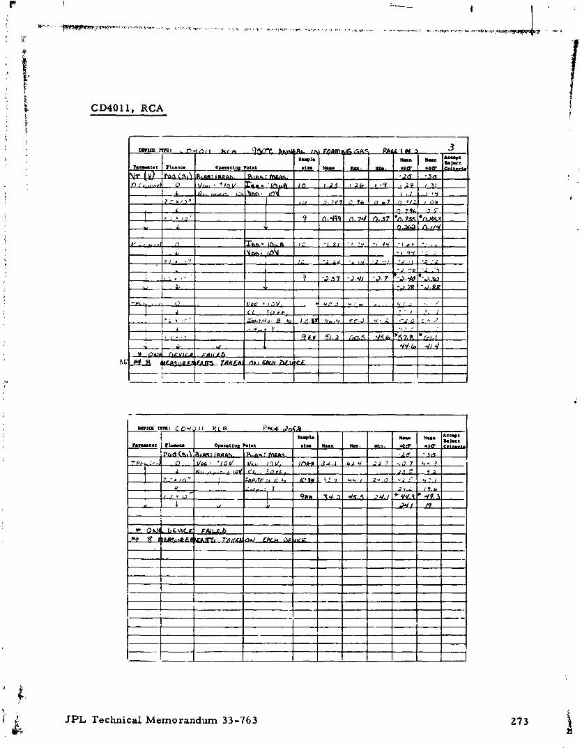
CD4011, RCA
JPL Technical Memorandum 33-763

CD4012, RCA
JPL Technical Memorandum 33-763
- -- "

CD4013, RCA
Ilia.
JPL Technical Memorandum 33-763
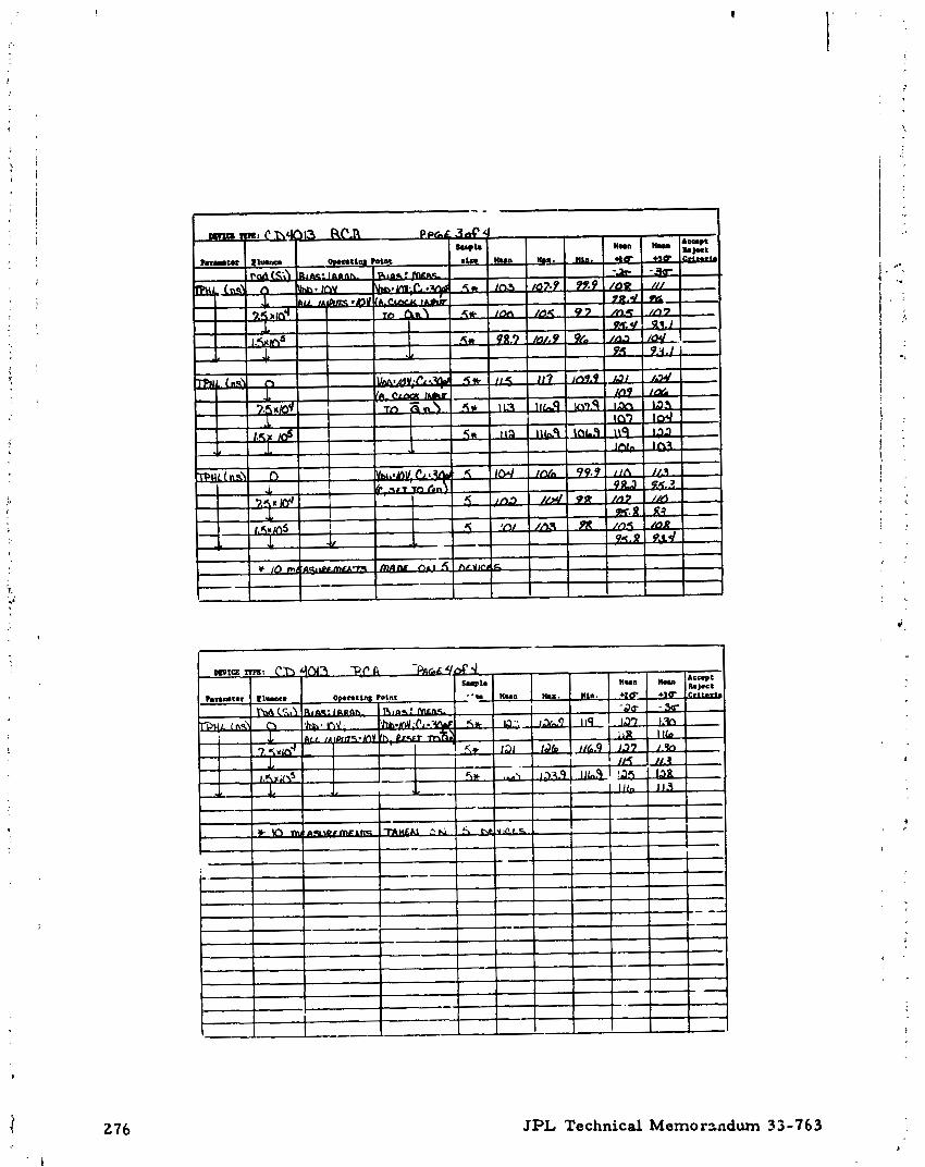
JPL Technical Memorzndum 33 -763
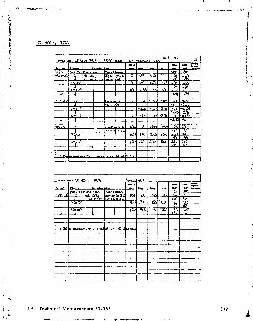
CA.4014, RCA
nu.
JPL Technical Memorandum 33- 76 3
- 9 I I I --_--_...I

C94015. RCA
JPL Technical ' (emorandurn 33-763

CD4016, RCA
JPL Technical Memorandum 33-763
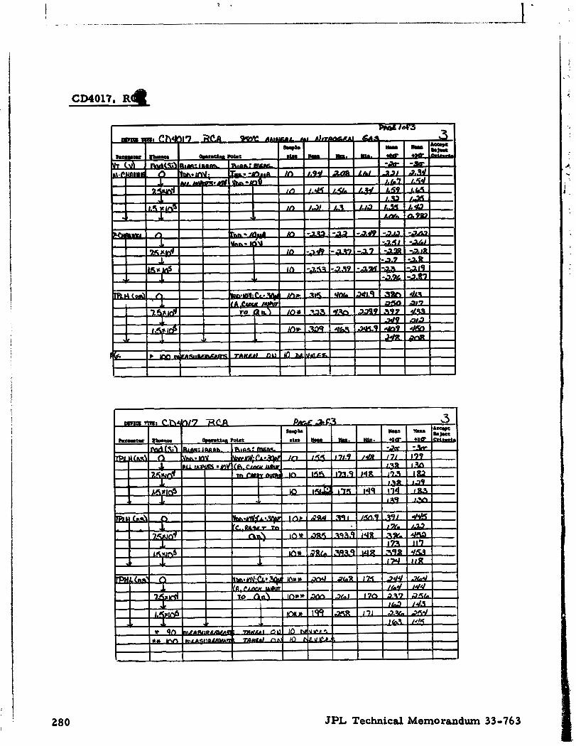
JPL Technical Memorandum 33-763

CD4019, RCA
d
i JPL Technical Memorandum 33-763

JPL Technical Memorandum 33-763

CD4021, RCA
JPL Technical Memorandum 33-763

CD4023, RCA
R E P R O D U C B m OF THE OBI-AL PAGE I8 POOR
JPL Technical hdem~randum 33-763
.. . - ----- --

CD4025, RCA - I
JPL Technical Memorandum 33-763

CD4027, RCA
JPL Technical Memorandum 33-763

CD4028. RCA
JPL Technical Memorandum 33-763

CD4029, RCA
JRL Technical Memorandum 33-763
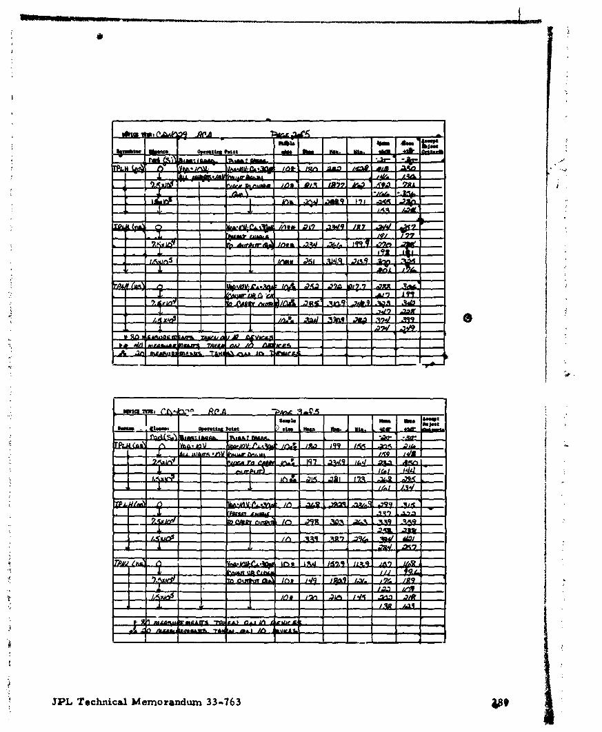
JPL Technical Memorandum 33-763

JPL Technical Memorandum 33-763

CD4030. RCA
JPL Technical Memorandum 33-763

CD4031. RCA
JPL Technical Memorandum 33-763
I 1 I
4 our c w F A I ~ .6
A&
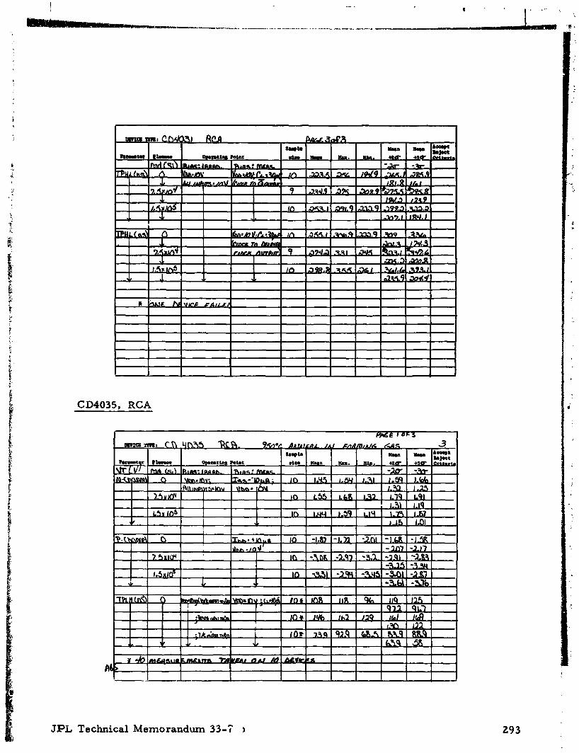
CD4035. RCA
JPL Technical Memorandum 33-7 > I
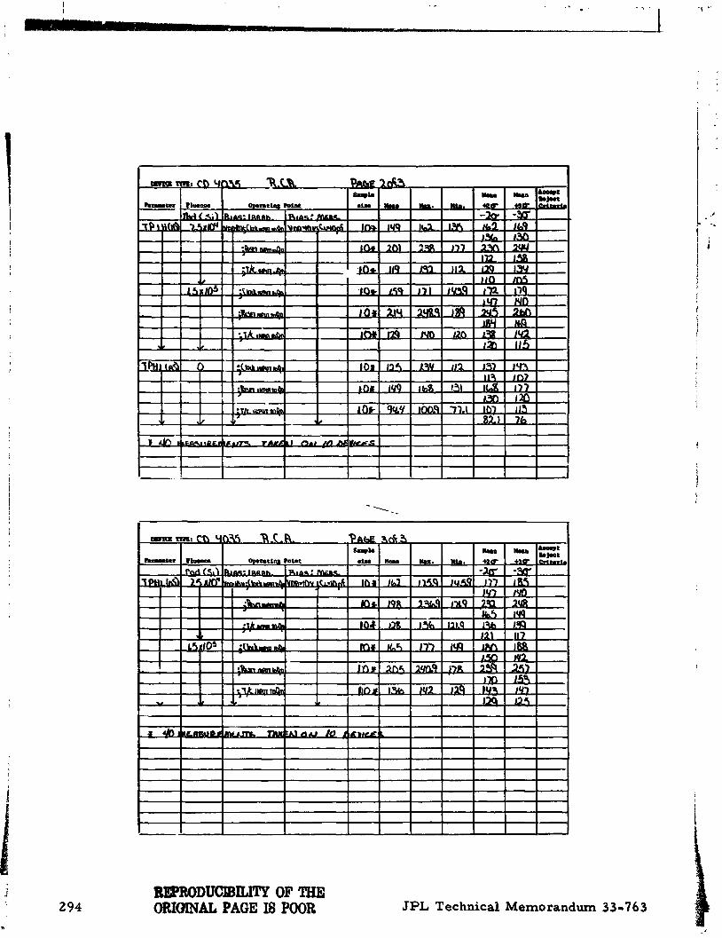
BEPRoDUmm OF THE ORIGINAL PAGE I8 POOR JPL Technical Memorandum 33-76 3

JI L Tachnical Memorandum 33-763

CD4042, RCA
JPL Te~hnical Memorandum 33-76 3

CD4043, RCA
i JPL Technical Memorandum 33-763 4

CD4047, RCA
REPRODUCIBILITY OF THE ORIGlNAL PAGE I8 POOR
JPL Technical Memorandum 33-76 3

JPL Technical Memorandum 33-763

JPL Technical Memorandum 33-76 3

JPL Technical Memorandum 33-763

CD4049, RCA
JPL Technical Memorandum 33-763

f 1
~ - - - - . . - - - - - . ,?:--~.h~-~--:'bM---- - ~ - ~ . . . . . , . . , , . . , . . , -.-----,*, , . I ,. . .r- ' . * . _ , . , .& ' 4 , .,' , , , . . ."I . ,, . . ./ ,-,- , ,,,:,,; .cic:,+Ei:*':.:,i. ,::;,xA,;;:L .%:?,',$. ,,,, ?w):.bsk: .,-,* .... ,,".;.i: .* +,'c:? '.! ::., : - , , .L~ '~ .~ . ! .~ ' .,,*,,, ,$- , " . . Z ? , ~ , . : L b,., , , , ,.,::. P , ".,, ., , , k > . , '
I., ..,,
1
GD4050. RCA
JPL Technicd Memorandum 33-763
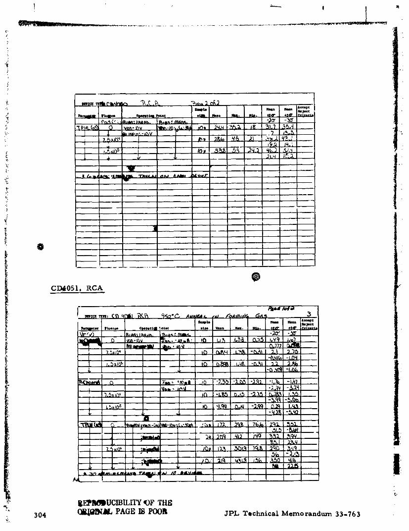
CD4051, RCA 49
@ E 2 ~ U C I B I L I T Y OF THE 304 PAGE I6 POOR JPL Technical Memorandum 33-76 3

C34052. RCA
JPL Technical Memorandum 33-763
I - .

CD4053. RCA
306 JPL Technical Memorandum 33-763 i
-- ._ _zC..----.llll.l-- 1- .-..---- --.------ 4 , . - - - a - . - , . - ... . ., , . . .,., . -... - . . ->, - . --

JPL Technical Memorandum 33-763

REFERENCES
I . Mnnroe, Theory of Probability, McGraw-Hill, New York, 1951.
2. Reiss, E. M. , and Vincoff, M. N. , "Effects of Variation of Gate- Oxide Anneal Temperature or Radiation Resistance and Reliability of C/MOS Devices, " paper presented at 1975 IEEE Annual Conferenre on Nuclear and Space Radiation Effects, July 14- 17, at Humboldt State University, Arcata, Calif.
3. Burghard, R. A. , Gwyn, C. W. . "Radiation Failure Modes in CMOS Integrated Circuits, " IEEE Trans. Nucl. Sci. , NS-20, Vol. 6, pp. 300-306, Dec. 1973.
4. Gregory, B. L. , "Process Controls for Radiation-Hardened Aluminum Gate Bulk Silicon CMOS, " paper presented a t 1975 IEEE Annual Conference on Nuclear and Space Radiation Effects, July 14-17, a t Humboldt State University, Arcata, Calif.
5. Srour, J. R. , et a l . , "Radiation Effects on Oxides, Semiconductors, and Devices," HDL-CR-75-171-1, i ia r ry Diamond Laboratory, Washington, D. C. , May 1975.
6. Yamakawa, K. A. , " ~ a t e / ~ n n e a l Measurements in RCA CMOS, " iOM 365-F-44-75, Jet Propulsion Laboratory, Pasadena, Calif., June 5, 1975 (an internal document).
JPL Technical Memo randurn 33-76 3

J P L alphabetical
code
A DI
ANA
CAD
CRC
CTI
DAL
DIK
EXR
FAS
GEC
HAR
HON
H P A
INL
KMC
MOT
NSC
PMI
APPENDIX A
VENDOR IDENTIFICATION CODE
FSCM number
Vendor
243 55 Analog Devices, Inc., Norwood, Mass
3 1855 Analog Technology Corpore tion
19647 Caddock Electronics, Div of Globe Union, Inc.
12517 Component Research Company. Inc .
Circuit Technology, Inc.
91637 Dale Electronics, Inc ., Subs. of the Lionel Corporation
12954 Dickson Electronics Corporation
52 06 3 Exar Integrated Systems, Inc.
07263 Fairchild Semiconductors, Div of Fai rchild Camera and Instrument Corp.
092 14 General Electric Company, Semi- conductor Products Dept.
91417 Harr is Semiconductor (Radiation, Inc. )
91929 Honeywell, Inc., Microswitch Division
2 8480 Hewlett- Packard Company
32293 Intersil Inc., Cupertino, Cal.
20754 KMC Semiconductor
14713 Motorola Semiconductor Products, Inc.
27014 National Semiconductor Corporation
06665 Precision Monolithics, Inc. , Santa Clara, California
JPL Technical Memorandum 33-763

JPL alphabetical
code
RAY
RCA
SET
SGN
SIL
SOD
TIX
T R W
UTR
WEC
FSCM number Vendor
Raytheon Company
RCA Corp., Solid State Division Somerville, N. J.
Semtech Corporation
Signetics Corp., Subs. of Corning Glass Works
Siliconix, Inc.
Solitron Devices, Inc.
Texas instruments, Inc., Semi- conductor Components Div.
T R W Semiconductor, Inc., (PSI)
Unit rode Corp.
Westinghousc Electric Corp., Semiconductor Division
310 JPL Technical Memorandum 33-763

APPENDIX B
RECOMMENDED WORST-CASE ELECTRONIC DEVICE PARAMETER VARIATIONS
The purpose of this appendix i s to provide recommendations to aid the
circuit designer in the worst-case analysis of circuits. The worst case
parameter variations contained in Tables B- 1 through B-6 for transistors,
resistors, fixed capacitors, diodes, TTL (transistor-transistor logic) and
linear integrated circuits, and CMOS integrated circuits a re recommendations
only and not hard requirements.
These tables do not include radiation-induced degradation. Radiation
degradation should be added to the variations in these tables on an individual
part basis where part data i s available. Estimates should be made otherwise.
Section 153 should be contacted when the worst-case analysis i s to be
performed.
4 JPL Techical Memorandum 33-763

Table B-1. Worst-case parameter variations for transistors
As an aid to the circuit designer's worst-case analyses, the maximum
expected parameter variations for system life and temperature a r e given.
It is noted that all parameter changes a r e based on the specific value given in
the application of JPL ST o r manufacturer specifications, except for hFE.
For this parameter the variation is from the design value as established by
appropriate design curves a t 25OC and the design value of IC. For the cases
of saturated switches, the parameter changes of hFE will be established from
the minimum value specified in the manufacturer specifications, or ST. The
data below appl'es to al l transistors listed in +he approved parts list.
Parameter - - -- - - -
Variations Conditions Remarks
h~~ O.g%/"c For temperature
-2570 For life
B V ~ BO - 10% For life and temperature
B V ~ ~ ~ -10% For life and temperature
B V ~ ~ ~ - 3070 For life and temperature
For life
M. 2mVI0C For temperature
For life and temperature
IC BO doubles every For temperature 10°C increase
-1-1 00% For life
doubles every For temperature 10%
+loo% For life
I
Change from design value mfr. spec.
Change from rnin. value in rnfr. spec.
Change f rom min. value in mfr. spec.
Change from min. value in mfr. spec.
Change from max. value in rnfr. spec.
Change from max. value in mfr. spec.
Change from max. value in rnfr. spec. a t 25OC
Change from max. value in mfr. spec. a t 25°C
Added to temperature effects
--
JPL Technical Memorandum 33-763

Table B-1 (contd)
Parameter Variations Condition s Remarks
For life and temperature
For &fe and temperature
For life and temperature
For life and temperature
For life and temperature
For life and temperature
For life and temperature
For life and temperature
Change from max. value in rnfr. spec.
Change from max. value in mfr, spec.
Change from max. value in rnfr. spec.
Change from max. value in rnfr. spec.
Change from max. value in mfr. spec.
Change from max. value in mfr. spec.
Change from max. value in rnfr. spec.
Change from min. value in rnfr. spec.
JPL Technical Memorandum 33-763

Table B-2. Worst-case parameter variations for resis tors
Pa r t de sc ription: Manufacturer Manufac tu r e r ' s Tolerance,
General, class, type type number Purchase Design a, b
Carbon comp.
Carbon comp.
Carbon comp.
Precision WW
Metal film
Metal film
Powe r wirewound
Metal glaze
Metal glaze
Metal film fixtrim
HI RES ( l o L 2 ohms)
Ultra high res.
Ultra high res.
ABC
ABC
ABC
SHA
MEP ANG
MEP ANG
DAL
CAD
CAD
ANG
W E L
RCR05
RCRO7
RCR20
HR ser ies
RNC55H
RWR series
MG, MH ser ies
MM series
IV-5
i 5
*5
i 5
i o . 1
i l
a ~ e s i g n tolerance includes purchase, temperature, and end-of-life tolerances except where noted.
b ~ e s i g n tolerance does not include temperature and voltage coefficient effects for which the JPL ST or mfg. spec. should be consulted.
JPL Technical Memorandum 33-763

Table B-3. Worst-case parameter variations for fixed capacitors
P a r t description: Manufacturer's Tolerance, 70 General, s ~ l a s s , type Manufacturer type numbe r Purchase ~ e s i ~ n ~
Solid tantalum SPR CSRl3 - KS *lo *20
Ceramic AUX CKR05BX - KS a10 *2 5
Ceramic AUX CKR06BX - KJ *10 *2 5
Ceramic AUX CKRllBX - KR *1 0 e 5
Ceramic AUX CKR12BX - KI?, *10 *2 5
Ceramic AUX CKR14BR - KR *1 0 *30
Ceramic AUX CKR15BR - KR *10 *30
Ceramic, AUX MLlO MC70 A5 i12 temp. comp. MLl l MC90
Ceramic, HV disc. ERIE 800 beries *lo *17
Glass CGW CYFR ser ies *l i2 .1
Cleramic, CYL, AX. AUX HRMC 706A, T BD T BD 206A, 866A, 906A
Porcelain VIT V Y ser ies TBD T BD
Poly sulfone CRC MP ser ies T BD T BD
MICA ELM HRDM T BD T BD
a Pesign tolerance includes purchase, temperature, and end-of-life tolerances except where noted.
JPL Technical Memorandum 33-763

Table B-4. Worst-case parameter variations for diodes, Zener diodes
As an aid to the circuit designer's worst-case analyses, the maximum
expected parameter variations for system life and temperature a r e given.
It is noted that all parameter changes a r e based on the specific value given
in the applicable manufacturer's specification o r JPL ST.
Diodes ~ -
Parameter Variation Conditions Remarks
v~ *lOOIo For life Change from value in mfr. spec.
t150 mV For temperature
C t250/0 For life and Change from value in mfr. spec. temperature
tr +lo% For life and Change from value in rnfr. spec. temperature
IR 1OX For life Change from value in mfr. spec.
(a) For temperature Change from value in rnfr. spec.
B~ - 40% For life and Change from value in rnfr. spec. temperature
Zener diodes
V~ T *5 70 For life and Added to tolerance in mfr. spec. temperature
'zr +lo70 For life and Change from value in mfr.. spec. te mpe rature
T~ +100/0 For life and Change f , a m value in mfr. spec. temperature
IR 30X For temperature Change from value in mfr, spec.
1OX For life
v~ +10% For life and Change from value in mfr. spec. temperature
a ~ o u b l e s for every 10°C increase in temperabre.
31 6 JPL Technical Memorandum 33-763

Table B-4 (contd)
Voltage reference diode
Parameter Variation Conditions Remar).
Temp. Coef.
For lite and temperature
Change to tolerance in rnf r. spec.
For temperature Change from vdue in mfr. spec.
For life
For life and temperature
4.10% For life
Change from value in mfr. spec.
Added to temperature coeCticiat for temperature variations
Note: Consul twithpartspecial is tsonl ife stabilityfactors.
JPL Technical Memorandum 33-763

Table B-5. ~ o r * c a e e parameter va ja t ione for integrated circuits
Ae aid to h e circuit designerle worst-caee analyses, the maxin~unr
expeeed parameter variations for system li. e and temperature a r e $ven.
All p a r a m a e r changee listed a r e baeed on the speciac value given in the
applicable JPL ST. T h e data below apply to al l IC1e listed in rhe approved
parts list.
Digital IC1s (TTL and *ow power "ML)
Parameter V a r i e o c s , '70 Conditions
Vou ~ ( 0 )
OUT(^) I
I IN(#
IN(O) IOTJ T@
I o s
PDH
T~~~
Icc Clock pulse width
Life and temperature
Life and temperature
Life and temperature
Life and temperature
Life and temperature
Life and temperature
Life and temperature
Life and ten :I.. , r l . :
Life and temperature
Life and temperature
Linear IC1e
A v ~ ~ *40 Life and temperature
1 BIAS AVOS /a T -0s
Icc
IEE
Life and temperature
Life and temperature
Life and te mpe rature
Life and temperature
Life and temperature
Life mid tepperature
Life and ttmperature
Life and temperature
318 RmDUC#iILITY OF TIIE "
ORIGINAL PAGE IS POOR JPL Technical Memorandum 33-76 3

Table B-6. Worst-case parameter variations for CMOS integrated circuits
As an aid to the circuit designer's worst-case analyses, the maximum
expected parameter variations for system life and temperature a r e given.
All parameter changes listed a r e based on the specific value given in th,.
applicable specification control drawing. The data below apply to al l CMOS
listed in the approved parts lists.
Variations, Yo Variations, Yc/"C Parameter (life) (temperature) Remarks
No D G load
Iss *5 0 t10 Quiescent current
.TPL Technical Memorandum 33-763

APPENDIX C
PARAMETER VALUES O F IC TYPES REQUIRING RADL4TION ACCEPTANCE PRIOR TO FLIGHT USE
The various approaches being used to establish radiation acceptability
of certain IC types prior to flight use a r e the following:
(1) Use a modified o r standard manufacturing process combined
with a sample radiation tes t of each lot built.
( 2 ) Irradiate /anneal (IRAN) a l l of the devices to be used.
(3) IRAN a sample from each lot. In this case, the devices sub-
jected to IRAN as well a s the lot balance a r e considered suitable
for flight.
The starting vzlues of the device parameters and the parameter changes
due to the Jovian environment a r e related to the radiation acceptance approach
employed. For the sake of completeness, IC's that were not radiation-screened
but were used by the subsystems, a r e included.
All IC types (except CMOS) currently being subjected to one of the
above approrches to establish radiation acceptability prior to flight use .Ire
listed in Table C-1 together with the specific parameters being controlled.
Room t e m p e r a t u r ~ parameter values a re given for the following cases.
Initial: Starting worst case values of parameters when the
devices a r e supplied to JPL.
Post-IRAN: Worst case parameter values after devices have been
subjected to IRAN. Hence, for devices subjected to
IRAN, these would be the parameter values a t the time
of initial installation into flight hardware.
Post- JupitL r: Anticipated worst case parameter values after devices
have been through the Jovian environment. Values a r e
given for assumed doses of 12.5, 30, 60 and 125 krads.
Note that for some device types the parameter values may exceed the manu-
facturer 's normally specified limit when the devices a r e initially installed.
Subsystems requiring better parameter values than those in the table must
JPL Technical Memorandum 33-76 3
1. ... -----
-.--I Y I

resort to shielding. Parameters other than those listed in the table may also
be affected by radiation, but have not been identified via the GE circuit anal-
yses as being critical to the applications and are not subject to control.
JPL Technical Memorandum 33-763

JPL TechrAical Memorandum 33-763
_._,_ -. - .--- \

Tab
le C
- 1
(c on
td)
Init
ial
Po
st -
Po
st - J
up
ite
r v
alu
es
Man
u -
Pa
ram
ete
r P
art
ty
pe
fac
ture
r co
ntr
oll
ed
IR
AN
12.5
k
rad
3
0 k
rad
6
0 k
rad
1
25
kra
d
DG
129
SIL
DG
133
SIL
DG
141
SIL
DG
181
SIL
DG
Ml1
1
SIL
IS,
off
IS'
off
Is,
off
IS,
off
ID,
off
IS,
off
ID,
off
ID'
off
r D
st
on
rDS
# o
n
(A
)
1
(nA)
(dlb
(n
NC
(oh
ms)
b
a 25
nA f
or
no
nsc
reen
ed
pa
rts.
b~
= D
=-1
0 V
.
C S
= G
ND
, D
=1
0 V
.
1 5a
15
60
Fa
ile
d
Fa
ile
d
30
260
5 10
0
10
00
" .
. -
..""<
1
5 . .-
. .. L
.. ,
- ..,.a
U
-'A
.,,. c..-.-
.*- .-
,~
.*
L.
~-
~"
~b
l*
~~
,~
.~
~u
IY
I
*

w 3 3 3 3 Y Y Y Y Y Y
JPL Technical Memorandum 33-763

i JPL Technical Memorandum 33-763

0 f'l rl
K~PRODUCUSI l l'l'l . )!,' , JPL Technical Memorandum 33-763 OfiIGINAIA Pi\(; i; is' !:
------.----- - - - . . .
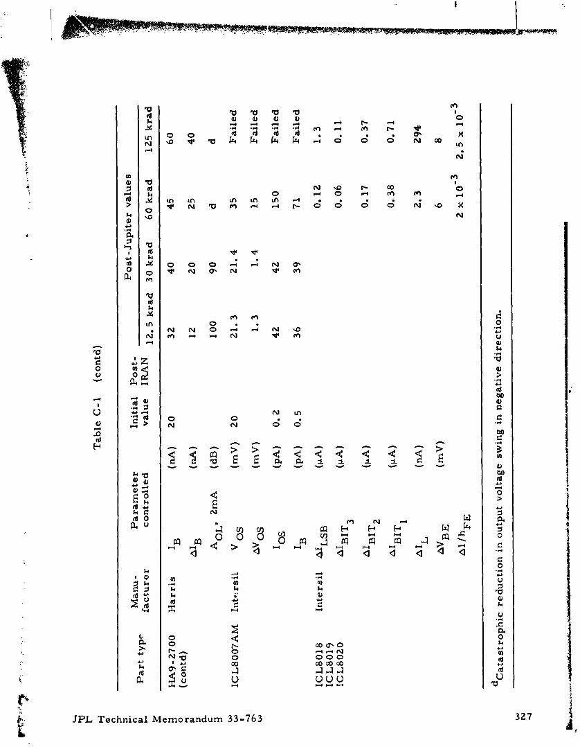
Ta
ble
C- 1
(c
on
td)
Po
st - J
up
iter
va
lues
M
anu
- P
ara
met
er
Init
ial
Po
st-
Pa
rt t
yp
e fa
ctu
rer
con
tro
lled
IR
AN
12.5
kra
d 30 krad
60 k
rad
125 k
rad
HA9-2700
Ha
rris
(c
on
td)
ICL8018
Inte
rsil
ICL8019
ICL8020
60
40
d Failed
Fa
iled
Fa
iled
Fa
iled
1.3
0.11
d~
ata
str
op
hic
red
uct
ion
in
ou
tpu
t v
olt
ag
e sw
ing
in
neg
ati
ve
dir
ecti
on
.

JPL Technical Memorandum 33-763
4
, *"+ +*-t-*.~

4 4 4 E E E
JPL Technical Memorandum 33-763 329
. - --, ..-A, ' . . . . .

Ta
ble
C- 1
(c
oL
~~
)
Po
st -
Ju
pit
er
va
lue
s M
anu
- P
ara
me
ter
Init
ial
Po
st-
p
art
typ
e fa
ctu
rer
co
ntr
oll
ed
IR
AN
1
2.5
kra
d
30
kra
d
60
kra
d
12
5 k
rad
-
(mV
) 0
.9
1.0
1
.1
1.3
5
1.6
5
Lh
il0
8A
H
NS
C
(Ha
rd)
vo
~
(mV
) 0.
1
0.
2
0.4
5
0.7
5
LM
10
8
NS
C
v~~
(mV
) 2
.0
(Un
ha
rd)
(m
v)
Io
s
(nA
) 0
.2
O1
os
(nA)
I B
(nA)
2.0
A I
B
(A
)
A~
~'
2
mA
(d
q)
2. 3
2.
5
59
1
05
2
0. 3
0.
5
5 7
10
50
0.6
1
.6
6.6
6
.7
0.4
1
.4
6.4
6
.5
3.7
6.
5
13
.3
13
.6
1.7
4.
5
11
.3
11
.6
- F
ail
ed
-
-

Ta
ble
C-1
(c
on
td)
M a
nu
- P
ara
me
ter
Init
ial
Po
st-
Po
st-
Jup
ite
r v
alu
es
Part
ty
pe
fa
ctu
rer
co
ntr
oll
ed
lR
AN
1
2.
5 k
rad
30
ir
ad
6
0 k
rad
1
25
kra
d
LM 1
08
H
NS
C
(Ha
rde
ne
d)
~k
l0
8~
~
NS
C
(Ha
rde
ne
d
lot
C!
23
3A
)
LM
11
1F
N
SC
L
M1
11
H
WA
N)
v~
(mv
) 2
Av 0s
fniv
IOS
(n
A)
0. 5
*IO
S
(n
~
j
IB
(nA
) 4
%IE
(nA
)
A~
~'
2 M
A
(db
)
v 0s
!m
V)
2
AV
0s
(mv
!
e~
th
ea
p
ara
me
ters
ar
e t
he
sa
me
as f
or
the
ha
rde
ne
d L
Ml0
8.

cn o m a n - I n a 4

Ta
ble
C-1
(c
on
td)
Ma
nu
- P
ara
me
ter
Part
ty
pe
fac
ture
r c
on
tro
lle
d
Init
ial
Po
st-
P
os
t- J
up
ite
r v
alu
es
IRA
N 1
2.
5 k
rad
39
kra
d
60
kra
d
12
5 k
rad
0s'
off
(m
V)
5 1
7.
5
Fa
ile
d
Fa
ile
d
Fa
ile
d
AV
OS
- o
ff
(mV
) i2
. 5
Fa
ile
d
Fa
ile
d
Fa
ile
d
Ios '
off
(n
A)
25
3
5 F
ail
ed
F
ail
ed
F
ail
ed
A1
~~
s
o ff
(n
A)
10
F
ail
ed
F
ail
ed
F
ail
ed
IB,
off
(n
A)
10
0
21
0
Fa
ile
d
Fa
ile
d
Fa
ile
d
AIB
, o
ff
(nA
1
10
F
ail
ed
F
ail
ed
F
ail
ed
AIS
ink,
o
n
(mA
) -7
. 0
-1
4
- 22
- 2
8
hIs
ink
s 5
0%
(m
A
-6.
0
- 14
-2
2
-23
du
ty c
yc
le
off
(m
A)
-7.
0
Fa
ile
d
Fa
ile
d
Fa
ile
d
g~
ul
l
vo
lta
ge
= 0
.7
V.
-

Tab
le C
-1
(co
ntd
)
Man
u-
Pa
ram
ete
r ln
itia
l P
ost
- P
ost-
Ju
pit
er
va
lue
s
Part
ty
pe
fac
ture
r c
on
tro
lle
d
"due IRAN
12.
5 k
rad
30 k
rad
6
0 k
rad
1
25
kra
d
LM
13
9
NS
C
lJo
Ss
0"
(Un
ha
rd)
0s'
off
Av 0s
' off
loss
0"
AIo
sl
on
=os*
off
AIo
s,
off
IBr
On
AIB
B o
n
IBl
off
AIg
, of
f
5. 5
0. 5
Fa
ile
d
Fa
ile
d
34
9 Fa
ile
d
Fa
ile
d
23
0
13
0
Fa
ile
d
Fa
ile
d
- 7 Fa
ile
d
5. 6
0. 6
Fa
ile
d
Fa
ile
d
4 7
22
Fa
ile
d
Fa
ile
d
315
21 5
Fa
ile
d
Fa
ile
d
- 9
Fa
ile
d
6. 0
1. 0
Fa
ile
d
Fa
ile
d
10
5
80
Fa
ile
d
Fa
ile
d
52
5
42
5
Fa
ile
d
Fa
ile
d
-11
Fa
ile
d

Ta
ble
C-1
(c
on
td)
Pa
rt
typ
e
Ma
nu
- fa
ctu
rer
Po
st-
Ju
pit
er
va
lue
s P
ara
me
ter
Init
ial
Po
st-
c
on
tro
lle
d
IRA
N
12
. 5
kra
d
30
kra
d
60
kra
d
12
5 k
rad
LM
13
9
NS
C
0s' o
n
(Ha
rd)
Av
0s'
on
0s' o
ff
OV
0s' o
ff
AIo
s,
on
IOS
' o
ff
AIO
S,
off
IB'
0"
AIB
' o
n
Ig,
off
AIB
' o
ff O
n
'sin
k'
off
A1
~in
k' o
ff
7 2
Fa
ile
d
Fa
ile
d
10
0
75
Fa
ile
d
Fa
ile
d
60
0
50
0
Fa
ile
d
Fa
ile
d
1. 7
-9.
9
Fa
ile
d
Fa
ile
d

JPL Technical Memorandum 33-763 N A U - J R - C m r ~ L A c.lr