Quantifying the environmental footprint of semiconductor equipment using the environmental value...
10
eScholarship provides open access, scholarly publishing services to the University of California and delivers a dynamic research platform to scholars worldwide. Laboratory for Manufacturing and Sustainability UC Berkeley Peer Reviewed Title: Quantifying the Environmental Footprint of Semiconductor Equipment Using the Environmental Value Systems Analysis (EnV-S) Author: Krishnan, Nikhil , UC Berkeley Raoux, Sebastien Dornfeld, David , UC Berkeley Publication Date: 01-01-2004 Series: Green Manufacturing and Sustainable Manufacturing Partnership Publication Info: Green Manufacturing and Sustainable Manufacturing Partnership, Laboratory for Manufacturing and Sustainability, UC Berkeley Permalink: http://escholarship.org/uc/item/78g5824b Additional Info: Krishnan, N., Raoux, S., and Dornfeld, D. (2004), "Quantifying the Environmental Footprint of Semiconductor Process Equipment using the Environmental Value Systems (EnV-S) Analysis", IEEE Trans. Semiconductor Manufacturing, 17, 4, pp. 554-561. Keywords: cost of ownership, design for environment (DFE), environmental impact Abstract: Many environmental and health impacts from semi- conductor processing are tied to the design of the manufacturing equipment. Evaluating solutions to properly treat effluents from semiconductor tools has become an increasingly important part of supply chain management and equipment procurement deci- sions. Accordingly, understanding the environmental footprint associated with equipment sets is essential for both equipment manufacturers and semiconductor manufacturers seeking to improve their products’ environmental and financial perfor- mance. Equipment environmental performance must be evaluated within the context of the factory infrastructure and auxiliary equipment sets, with appropriate allocations of impacts from additional steps, both upstream and downstream of the wafer processing tools (chemical precursor delivery as well as byprod- ucts treatment). Several challenges to environmental assessments arise from the nature of semiconductor manufacturing itself, due to short process life cycles, complexity of processes,
-
Upload
independent -
Category
Documents
-
view
1 -
download
0
Transcript of Quantifying the environmental footprint of semiconductor equipment using the environmental value...
eScholarship provides open access, scholarly publishingservices to the University of California and delivers a dynamicresearch platform to scholars worldwide.
Laboratory for Manufacturing andSustainabilityUC Berkeley
Peer Reviewed
Title:Quantifying the Environmental Footprint of Semiconductor Equipment Using the EnvironmentalValue Systems Analysis (EnV-S)
Author:Krishnan, Nikhil, UC BerkeleyRaoux, SebastienDornfeld, David, UC Berkeley
Publication Date:01-01-2004
Series:Green Manufacturing and Sustainable Manufacturing Partnership
Publication Info:Green Manufacturing and Sustainable Manufacturing Partnership, Laboratory for Manufacturingand Sustainability, UC Berkeley
Permalink:http://escholarship.org/uc/item/78g5824b
Additional Info:Krishnan, N., Raoux, S., and Dornfeld, D. (2004), "Quantifying the Environmental Footprint ofSemiconductor Process Equipment using the Environmental Value Systems (EnV-S) Analysis",IEEE Trans. Semiconductor Manufacturing, 17, 4, pp. 554-561.
Keywords:cost of ownership, design for environment (DFE), environmental impact
Abstract:Many environmental and health impacts from semi- conductor processing are tied to the design ofthe manufacturing equipment. Evaluating solutions to properly treat effluents from semiconductortools has become an increasingly important part of supply chain management and equipmentprocurement deci- sions. Accordingly, understanding the environmental footprint associated withequipment sets is essential for both equipment manufacturers and semiconductor manufacturersseeking to improve their products’ environmental and financial perfor- mance. Equipmentenvironmental performance must be evaluated within the context of the factory infrastructureand auxiliary equipment sets, with appropriate allocations of impacts from additional steps, bothupstream and downstream of the wafer processing tools (chemical precursor delivery as well asbyprod- ucts treatment). Several challenges to environmental assessments arise from the natureof semiconductor manufacturing itself, due to short process life cycles, complexity of processes,

eScholarship provides open access, scholarly publishingservices to the University of California and delivers a dynamicresearch platform to scholars worldwide.
and the need to track diverse inter-related impacts. Environmental value systems analysis (EnV-S)is an analytical tool to evaluate the environmental performance of semiconductor processing. EnV-S develops environmental assessments through a “bottom-up” analysis approach, assemblingequipment environmental models to describe a system. This paper presents the use of EnV-Sas a tool to quantify the environmental impact of a product or process by creating an operationalsignature along multiple dimensions of cost and environmental and health factors. The use ofEnV-S is illustrated through a case study comparing systems that abate emissions from dielectricchemical vapor deposition processes.
554 IEEE TRANSACTIONS ON SEMICONDUCTOR MANUFACTURING, VOL. 17, NO. 4, NOVEMBER 2004
Quantifying the Environmental Footprint ofSemiconductor Equipment Using the Environmental
Value Systems Analysis (EnV-S)Nikhil Krishnan, Sebastién Raoux, and David Dornfeld
Abstract—Many environmental and health impacts from semi-conductor processing are tied to the design of the manufacturingequipment. Evaluating solutions to properly treat effluents fromsemiconductor tools has become an increasingly important partof supply chain management and equipment procurement deci-sions. Accordingly, understanding the environmental footprintassociated with equipment sets is essential for both equipmentmanufacturers and semiconductor manufacturers seeking toimprove their products’ environmental and financial perfor-mance. Equipment environmental performance must be evaluatedwithin the context of the factory infrastructure and auxiliaryequipment sets, with appropriate allocations of impacts fromadditional steps, both upstream and downstream of the waferprocessing tools (chemical precursor delivery as well as byprod-ucts treatment). Several challenges to environmental assessmentsarise from the nature of semiconductor manufacturing itself,due to short process life cycles, complexity of processes, and theneed to track diverse inter-related impacts. Environmental valuesystems analysis (EnV-S) is an analytical tool to evaluate theenvironmental performance of semiconductor processing. EnV-Sdevelops environmental assessments through a “bottom-up”analysis approach, assembling equipment environmental modelsto describe a system. This paper presents the use of EnV-S as atool to quantify the environmental impact of a product or processby creating an operational signature along multiple dimensionsof cost and environmental and health factors. The use of EnV-Sis illustrated through a case study comparing systems that abateemissions from dielectric chemical vapor deposition processes.
Index Terms—Cost of ownership, design for environment (DFE),environmental impact.
I. INTRODUCTION
AS THE semiconductor sector is growing rapidly, theneed to reduce the environmental and health impacts of
semiconductor processing is growing in importance. Since alarge portion of the environmental impact of semiconductorchips may occur during chip manufacturing, it is essentialto understand the manufacturing equipment’s environmentalperformance [1].
Manuscript received October 29, 2003; revised May 28, 2004. This work wassupported in part by the University of California, Berkeley, by Applied Mate-rials, Inc., by the NSF/SRC Engineering Research Center on EnvironmentallyBenign Semiconductor Manufacturing, University of Arizona, and the NationalScience Foundation under Grant DMI-0200204.
N. Krishnan is with Columbia University, New York, NY 10027 USA (e-mail:[email protected]).
S. Raoux is with Applied Materials, Inc., Santa Clara, CA 94054 USA(e-mail: [email protected]).
D. Dornfeld is with the University of California, Berkeley, CA 94720-1750USA (e-mail: [email protected])
Digital Object Identifier 10.1109/TSM.2004.835705
EnV-S is a “bottom-up” equipment-centric approach tosupport both the analysis of environmental, health, and safety(EHS) implications and the design of semiconductor manufac-turing processes. A “bottom-up” approach offers the flexibilityin analysis required by designers and buyers. This paper focuseson the use of EnV-S methodology to evaluate the environmentaland health “footprint” of equipment sets, specifically guidingthe choice of exhaust treatment systems.
The use of EnV-S as a qualification tool is illustrated througha case study in abating emissions from a dielectric chemicalvapor deposition (DCVD) process. DCVD is selected foranalysis in this paper because it currently represents the fab’slargest gaseous emissions contributor. In particular, fluorinatedcompound emissions from this process require treatment,especially during DCVD chamber cleaning. The case study inthis paper focuses on a DCVD undoped silicate glass (USG)process module used as an insulating dielectric material in asemiconductor device [2], [3].
EnV-S compares the overall environmental footprints of fourdifferent technologies to treat DCVD air emissions: combustionand water scrubbing, electric oxidation and water scrubbing,hot-bed, and cold-bed technologies. The comparisons pre-sented in this paper are representative of generic technologiesrather than specific products. In practice, EnV-S data can alsorepresent specific equipment configurations, rather than thebroader technology comparison presented here. The followingsections discuss the scope and methodology of EnV-S, theenvironmental metrics used, and the kinds of analyses anddecisions that are offered by the model.
II. BRIEF REVIEW OF SEMICONDUCTOR ENVIRONMENTAL
DESIGN TOOLS AND STUDIES
There have been several previous approaches to developingenvironmental design and evaluation tools for the semicon-ductor industry. The computerized assessment of relative risk(CARRI) [4], [5] is a risk assessment tool, based on toxicitydata, that aims to compare the relative risks of alternativemanufacturing processes with respect to mass/flow and ex-posure information. The environmental and health metricssupported by CARRI require the use of SEMATECH S70 [6](a mass balance tool). The principle challenges in CARRI andS70 appear to be the large toxicological data requirement andissues with proprietary information sharing among the membercompanies. The cost of ownership (CoO) metrics supportedby CARRI require the use of the SEMATECH EHS CoO tool[7], [8] that focuses on environmental costs and allows forsensitivity analysis of cost to input parameters. Other standard
0894-6507/04$20.00 © 2004 IEEE
KRISHNAN et al.: QUANTIFYING ENVIRONMENTAL FOOTPRINT OF SEMICONDUCTOR EQUIPMENT USING ENVIRONMENTAL VALUE SYSTEMS 555
CoO methods, such as the cost models developed by SEMI [9]and SEMATECH [10] do not explicitly focus on environmentalcosts.
A modular mass/flow evaluation tool E has been developedby Galli et al., [11] based on a top-down facility-scale evalua-tion. A facilities-level input–output approach, however, does notlend itself to understanding equipment details.
To provide the flexibility needed to develop predictive lifecycle inventories within facilities, Murphy has developed amodule-based parametric analysis of semiconductor environ-mental impacts [12]. This module-based analysis is not directlyequipment-centric, but it could support equipment DFE efforts.
Environmental analysis of semiconductors has been pro-gressing toward life cycle assessment (LCA). Although a fewLCA and large system-scale studies have been conducted[1], [13]–[16], a generic LCA tool to support semiconductormanufacturing does not yet exist. Challenges still remain indeveloping LCA tools to keep pace with technology changes,handle uncertainty and inform detailed equipment decisionmaking.
III. SCOPE AND METHODOLOGY OF EnV-S
The current scope of EnV-S includes “within-facility” im-pacts, including semiconductor manufacturing and downstreamdisposal operations that represent real environmental costsborne by semiconductor manufacturers. However, the analysiscan be expanded to include additional impacts in conjunctionwith other life cycle tools. The analysis proceeds in three stages[17]–[19].
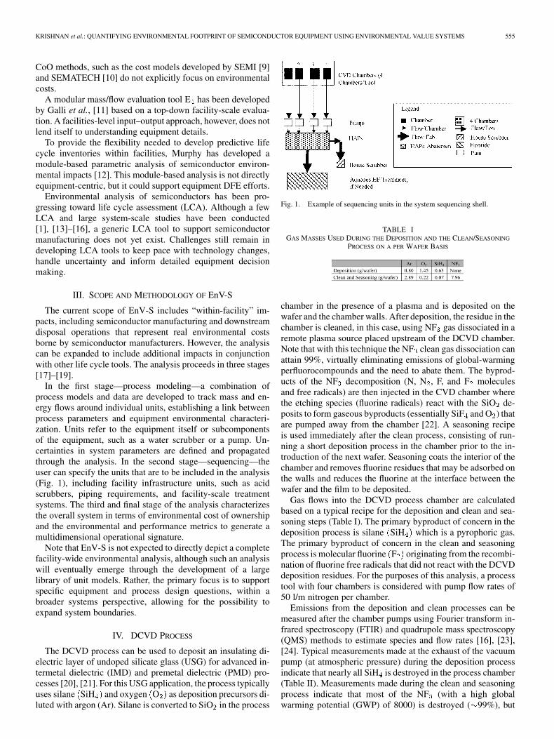
In the first stage—process modeling—a combination ofprocess models and data are developed to track mass and en-ergy flows around individual units, establishing a link betweenprocess parameters and equipment environmental characteri-zation. Units refer to the equipment itself or subcomponentsof the equipment, such as a water scrubber or a pump. Un-certainties in system parameters are defined and propagatedthrough the analysis. In the second stage—sequencing—theuser can specify the units that are to be included in the analysis(Fig. 1), including facility infrastructure units, such as acidscrubbers, piping requirements, and facility-scale treatmentsystems. The third and final stage of the analysis characterizesthe overall system in terms of environmental cost of ownershipand the environmental and performance metrics to generate amultidimensional operational signature.
Note that EnV-S is not expected to directly depict a completefacility-wide environmental analysis, although such an analysiswill eventually emerge through the development of a largelibrary of unit models. Rather, the primary focus is to supportspecific equipment and process design questions, within abroader systems perspective, allowing for the possibility toexpand system boundaries.
IV. DCVD PROCESS
The DCVD process can be used to deposit an insulating di-electric layer of undoped silicate glass (USG) for advanced in-termetal dielectric (IMD) and premetal dielectric (PMD) pro-cesses [20], [21]. For this USG application, the process typicallyuses silane SiH and oxygen O as deposition precursors di-luted with argon (Ar). Silane is converted to SiO in the process
Fig. 1. Example of sequencing units in the system sequencing shell.
TABLE IGAS MASSES USED DURING THE DEPOSITION AND THE CLEAN/SEASONING
PROCESS ON A PER WAFER BASIS
chamber in the presence of a plasma and is deposited on thewafer and the chamber walls. After deposition, the residue in thechamber is cleaned, in this case, using NF gas dissociated in aremote plasma source placed upstream of the DCVD chamber.Note that with this technique the NF clean gas dissociation canattain 99%, virtually eliminating emissions of global-warmingperfluorocompounds and the need to abate them. The byprod-ucts of the NF decomposition (N, N , F, and F moleculesand free radicals) are then injected in the CVD chamber wherethe etching species (fluorine radicals) react with the SiO de-posits to form gaseous byproducts (essentially SiF and O ) thatare pumped away from the chamber [22]. A seasoning recipeis used immediately after the clean process, consisting of run-ning a short deposition process in the chamber prior to the in-troduction of the next wafer. Seasoning coats the interior of thechamber and removes fluorine residues that may be adsorbed onthe walls and reduces the fluorine at the interface between thewafer and the film to be deposited.
Gas flows into the DCVD process chamber are calculatedbased on a typical recipe for the deposition and clean and sea-soning steps (Table I). The primary byproduct of concern in thedeposition process is silane SiH which is a pyrophoric gas.The primary byproduct of concern in the clean and seasoningprocess is molecular fluorine F originating from the recombi-nation of fluorine free radicals that did not react with the DCVDdeposition residues. For the purposes of this analysis, a processtool with four chambers is considered with pump flow rates of50 l/m nitrogen per chamber.
Emissions from the deposition and clean processes can bemeasured after the chamber pumps using Fourier transform in-frared spectroscopy (FTIR) and quadrupole mass spectroscopy(QMS) methods to estimate species and flow rates [16], [23],[24]. Typical measurements made at the exhaust of the vacuumpump (at atmospheric pressure) during the deposition processindicate that nearly all SiH is destroyed in the process chamber(Table II). Measurements made during the clean and seasoningprocess indicate that most of the NF (with a high globalwarming potential (GWP) of 8000) is destroyed ( 99%), but
556 IEEE TRANSACTIONS ON SEMICONDUCTOR MANUFACTURING, VOL. 17, NO. 4, NOVEMBER 2004
TABLE IIEMISSIONS MEASURED POSTPUMP
TABLE IIIOPTIONS FOR ABATEMENT
it is largely converted into fluorine F , which is hazardousbecause of its toxicity. House scrubbers are not recommendedfor fluorine abatement due to concerns associated with trans-port through the exhaust (corrosion) and the potential for crossreactions. Furthermore, house scrubbers can be overwhelmedby the excess fluorine from all deposition and etch processesin the facility. Point of use (POU) abatement systems are,therefore, recommended for DCVD applications. In general,POU systems may lead to reduced safety risks (ductwork fires,corrosion, exhaust restrictions, etc.) and reduced environmentalrisks (meeting emissions limits) [25].
V. DIELECTRIC CVD ABATEMENT
The emissions from the DCVD process include SiH , SiF ,, NF , and HF (Table II). In general, several feasible POU
technologies are available to treat those gases individually.However, the above gases can be present at any time in theabatement system; for example, one chamber can run a depo-sition process while the other chambers run a clean process.Therefore, a proper abatement system must be capable to treatany and all of the DCVD byproducts. This requirement leads tothe elimination of some technology options. It can be seen thatof the seven technology options considered, only four can reallybe used to treat all DCVD emissions: combustion and waterscrubbing, electric oxidation and water scrubbing, cold-bedadsorption and hot-bed adsorption technologies (Table III). Hotand cold chemical beds and oxidation and wet scrubbing tech-nologies are also among those recommended by SEMATECHfor POU abatement for oxide deposition applications [25].These four technologies are, therefore, studied further.
POU combustion systems use fuel such as methane or hy-drogen to combust toxic and other flammable and pyrophoricemissions [26]. The combustion of fluorine-rich emissions leadsto the conversion of F to HF gas, which is typically waterscrubbed within the POU unit into an aqueous form. Hot-bedsystems use heat to help the gases reach reaction temperaturesand then react with bed substrates. Some hydrides such as silane
SiH are thermally decomposed by heat. Bed substrates canbe made of a mixture of metals and base oxides such as lime.The metals react with fluorine, SiF , HF, etc., to form metalhalides which are then neutralized by a base, such as lime, toform salts [23]. Cold-bed systems use chemisorptive resins toadsorb and subsequently react with fluorine and can operate pas-sively at ambient temperatures [27]. Fluorine and other fluori-nated species are typically removed using bed materials madeof silica or metal oxides. Electric oxidation and water-scrubbingsystems use electric heat to break down the byproducts and mayuse hydrogen or water to convert F to HF. The HF is scrubbedout within the POU unit into an aqueous form. In this paper,an electric oxidation and water-scrubbing system that uses hy-drogen as a reagent is considered.
VI. EnV-S APPLIED TO EXHAUST MANAGEMENT EQUIPMENT
In this paper, numerous process models and data are used toestimate environmental cost of ownership (CoO) and environ-mental impacts (Table IV).
EnV-S includes all units downstream of the DCVD processtool that are involved in emissions treatment (Fig. 1). The anal-ysis, therefore, includes the primary POU abatement device(combustion and water scrubbing, hot-bed adsorption, cold-bedadsorption, and electric oxidation and water scrubbing) andany subsequent downstream treatment required. One upstreamfactor is also considered: greenhouse gas emissions fromelectricity generation. This is included to allow a comparisonbetween combustion systems that use fuel as an energy sourceand electric oxidation and hot-bed systems that use electricityas a source of energy. Since all four abatement technologiesuse the same chamber pumps, pump data and models are notdirectly included in the analysis. However, the pump flowrate is used to estimate the exhaust loading from the differentabatement devices and to calculate an exhaust cost associatedwith the use of the facility house scrubbers.
Following the chamber pump, the emissions pass throughone of four primary POU abatement technologies: combustionand water scrubbing, hot-bed adsorption, cold-bed adsorptionor electric oxidation and water scrubbing. The liquid wastefrom combustion and water-scrubbing and electric oxidationand water-scrubbing systems is then piped into a downstreamfacility-scale wastewater treatment system. The downstreamfluoride treatment uses sodium hydroxide and calcium hy-droxide to neutralize the HF waste and produce fluoride sludge.Both the hot-bed and the cold-bed systems do not requiredownstream fluoride treatment, but they generate spent bedcartridges which need disposal.
VII. EnV-S EXHAUST VALIDATION RESULTS
A. Environmental CoO
For each equipment subcomponent in the EnV-S, environ-mental costs are aggregated along numerous subcategories.The environmental CoO metric takes into account facilityinfrastructure, system, equipment, and production categoriesand builds on current industry CoO models [9], [10] and EHS
KRISHNAN et al.: QUANTIFYING ENVIRONMENTAL FOOTPRINT OF SEMICONDUCTOR EQUIPMENT USING ENVIRONMENTAL VALUE SYSTEMS 557
TABLE IVSUMMARY OF PROCESS MODELS AND DATA
CoO models [8]. The focus of the environmental cost is onthe purchase, installation, use, handling, training, monitoring,treatment, and disposal of process equipment inputs, outputs,
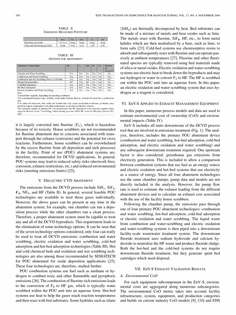
Fig. 2. Detailed costs of alternative abatement technologies.
and secondary flows (e.g., energy, exhaust, water, cleaningagents, dilution streams, etc). Total environmental costs of asystem are estimated as
(1)
where represents the number of unit cost models in a system,and are the fixed and operational costs ($/year) related
to unit , and is the number of wafers processed per year.Wafers processed are estimated based on wafer throughput,
uptime, and utilization of the equipment. Uptime is initially es-timated based on total production hours and scheduled mainte-nance and is then adjusted to include unscheduled downtimes.Major cost categories for the four systems appear in Fig. 2.
Capital and other fixed costs are depreciated over five years.Many operational cost categories are calculated by multiplyingannual usage data by unit costs. For instance, the annual elec-tricity costs for the combustion and water-scrubbing systemsare based on average usage ( 1.2 kW) and the cost of elec-tricity ( 6 cents/kWh for a typical U.S. fab) and are quite low( $600/annum). Hot-bed systems and electric oxidation andwater-scrubbing systems have higher electricity costs due to theneed for electric heating ( 3 and 5.6 kW, respectively). Mostconsumable costs for combustion and water-scrubbing systemsare related to fuel use and spares. For hot-bed and cold-bed ad-sorption systems, the consumable costs of new cartridges aresignificant and represent the primary operational costs of thesesystems. Treatment and disposal costs are high for combustionand water scrubbing and electric oxidation and water-scrubbingsystems because of the cost of treating fluoride-rich wastewater.
It can be seen that under nominal operating conditions,combustion and electric oxidation and water-scrubbing systemshave lower costs than cold- and hot-bed adsorption systems.The principle reason for the higher costs of cold- and hot-bedsystems are related to the cost of consumables. With an an-nual HF flow of 964 500 liters, the consumables cost of thehot-bed adsorption system is $1.49/wafer ( $192 900/year;$1800/cartridge with a capacity of 9000 l of HF; Table IV). The
558 IEEE TRANSACTIONS ON SEMICONDUCTOR MANUFACTURING, VOL. 17, NO. 4, NOVEMBER 2004
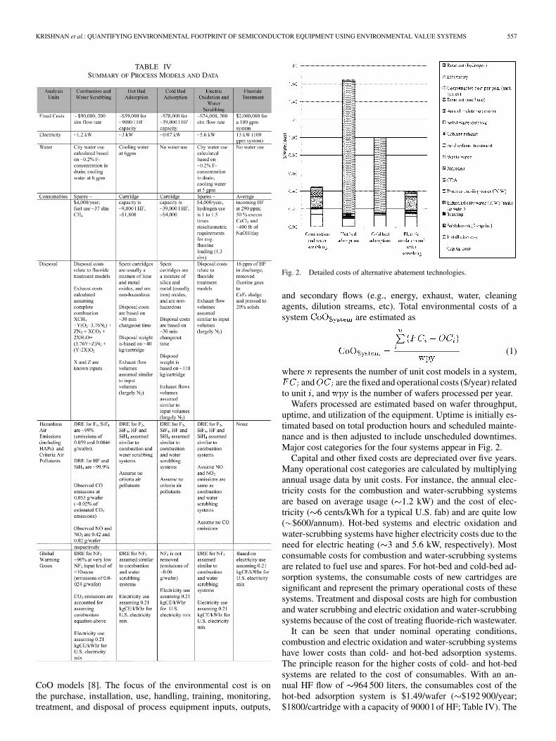
Fig. 3. Output cost uncertainties of technologies.
Fig. 4. Sensitivity analysis for combustion and water scrubbing.
column consumables cost of a cold-bed adsorption system is$0.83/wafer ( $107 000/year; $4328/column with a capacityof 39 000 l of HF; Table IV).
EnV-S also defines uncertainties for most inputs (includingcost, recipe, and facility parameters) and uses a Monte Carlosimulation to evaluate forecasts. For instance, the flow rate ofmethane can vary anywhere between 27–47 l/m with a nom-inal value of 37 l/m, and it can be represented by a triangulardistribution. A Monte Carlo simulation with 30 000 trials wasconducted for the four technologies. In looking at cost forecastsfollowing an uncertainty analysis, it can be seen that the com-bustion and electric oxidation and water-scrubbing technolo-gies represent a robust choice as the least expensive alternatives(Fig. 3). The upper and lower uncertainty bounds in Fig. 3 cor-respond to 2.5th and 97.5th percentile values, and the medianvalue is indicated by a short horizontal line.
Following a Monte Carlo simulation, sensitivity analysis ofoutput parameters is conducted using rank order correlation.The main effect on the cost of combustion and electric oxidationand water-scrubbing systems is from the cost of downstreamaqueous HF treatment and the flow of makeup water, with rankorder values of 0.96 and 0.22, respectively, for combustion andwater-scrubbing systems (Fig. 4). There is a large uncertaintyin the cost of treating aqueous HF, from 1 to 30 cents/gal, basedon data from facility-scale HF treatment systems. SEMATECHnumbers represent the high end of this scale ( $0.28/gal) [28].In the absence of a facility-scale treatment system, the use ofindependent contractors to haul-off HF waste could amount to$3/gal. Since a manufacturing facility is unlikely to operate withsuch high costs, this case for hauling HF waste is not considered.Cold-bed and hot-bed adsorption system costs are sensitive touncertainties in cartridge capacities, costs, and process factors(fluorine loading). For instance, there is significant uncertaintyrelated to capacity data for cold-bed cartridges (29 250–39 000 lof HF).
B. Environmental Metrics
The four technologies were compared relative to a set ofmetrics that track resources used, air emissions, and solid waste
TABLE VENVIRONMENTAL IMPACTS OF DCVD ABATEMENT
TECHNOLOGIES ON A PER WAFER PASS
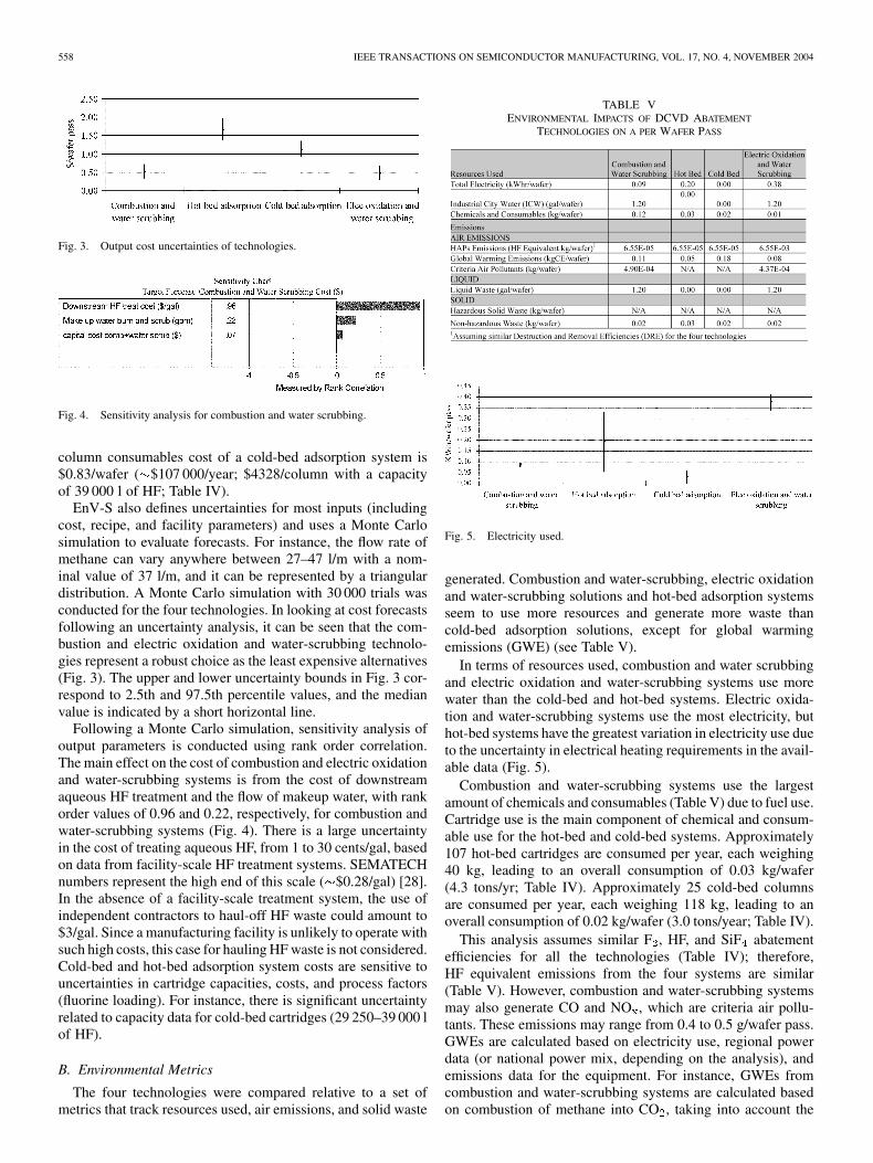
Fig. 5. Electricity used.
generated. Combustion and water-scrubbing, electric oxidationand water-scrubbing solutions and hot-bed adsorption systemsseem to use more resources and generate more waste thancold-bed adsorption solutions, except for global warmingemissions (GWE) (see Table V).
In terms of resources used, combustion and water scrubbingand electric oxidation and water-scrubbing systems use morewater than the cold-bed and hot-bed systems. Electric oxida-tion and water-scrubbing systems use the most electricity, buthot-bed systems have the greatest variation in electricity use dueto the uncertainty in electrical heating requirements in the avail-able data (Fig. 5).
Combustion and water-scrubbing systems use the largestamount of chemicals and consumables (Table V) due to fuel use.Cartridge use is the main component of chemical and consum-able use for the hot-bed and cold-bed systems. Approximately107 hot-bed cartridges are consumed per year, each weighing40 kg, leading to an overall consumption of 0.03 kg/wafer(4.3 tons/yr; Table IV). Approximately 25 cold-bed columnsare consumed per year, each weighing 118 kg, leading to anoverall consumption of 0.02 kg/wafer (3.0 tons/year; Table IV).
This analysis assumes similar F , HF, and SiF abatementefficiencies for all the technologies (Table IV); therefore,HF equivalent emissions from the four systems are similar(Table V). However, combustion and water-scrubbing systemsmay also generate CO and NO , which are criteria air pollu-tants. These emissions may range from 0.4 to 0.5 g/wafer pass.GWEs are calculated based on electricity use, regional powerdata (or national power mix, depending on the analysis), andemissions data for the equipment. For instance, GWEs fromcombustion and water-scrubbing systems are calculated basedon combustion of methane into CO , taking into account the
KRISHNAN et al.: QUANTIFYING ENVIRONMENTAL FOOTPRINT OF SEMICONDUCTOR EQUIPMENT USING ENVIRONMENTAL VALUE SYSTEMS 559
amount of NF and unreacted CH in the exhaust and electricityuse as follows:
(2)
where is the mass of greenhouse gas emitted (in kg/waferpass), is the global warming potential of gas (1 for CO ,23 for CH , and 10 800 for NF ) and GWEs from electricitygeneration are calculated using the following:
(3)
where electrical consumption is expressed in kilowatt hours perwafer pass. The factor of 0.21 kgCE/kWh reflects a typical U.S.electricity mix (this number may vary greatly depending on thegeneration mode of electrical power) [29].
Cold-bed adsorption systems have the largest global warmingimpacts, primarily because they cannot destroy NF . PostpumpNF emissions of 0.06 g/wafer pass are discharged from thesystem. Since NF has a GWP of 10 800, this emission causesa global warming impact of 0.18 kgCE/wafer pass followinga similar calculation as described in (2). For hot-bed adsorptionand electric oxidation and water-scrubbing systems, GWEs in-clude emissions from electricity generation.
Both combustion and electric oxidation and water-scrub-bing technologies generate liquid waste at approximately1.20 gal/wafer, with a variation from 0.89 to 1.51 gal/wafer.None of the systems generate hazardous solid waste. Hot-bedadsorption systems generate the most solid waste from dis-carded cartridges, which are sent to a nonhazardous landfill.
C. Health Metrics
Health impacts are evaluated based on a streamlined versionof the multicriteria hazard (MCH) evaluation technique [30],[31]. The MCH evaluation considers health and safety aspectsof process outputs under six categories: acute toxicity, systemictoxicity, reproductive/developmental toxicity, carcinogenicity,physical hazards, and standards and regulations. However,there are significant complications in understanding chemicalhealth effects in facilities, due to changing chemistries andinteracting agents [32], lack of data for numerous chemicals[33]–[36], and lack of health data for the six MCH categories.Therefore, EnV-S utilizes three of the MCH categories: acutetoxicity, physical hazards, and standards and regulations. Mul-tiple endpoints are considered under each category. Data forthese categories are frequently attainable in publicly availablehealth databases and material safety data sheets (MSDS). Theessentials of this hazard assessment technique are summarizedbelow. Further details are available in Thurwachter et al. [30],[31].
A chemical is assigned a score , for each category ,for every endpoint for which data are available. These scoresare assigned on a logarithmic scale from 1–10, based on thescaling factors. The overall category score for chemical in cat-egory , is then obtained by
(4)
TABLE VIHAZARD ASSESSMENT CATEGORY DATA CONVERTED TO LOGARITHMIC SCALE
where is the number of endpoints with available data forchemical and category .
The overall category score for a process stream with a mix-ture of chemicals in category , , is calculated by massweighting the logarithmic category scores of individual chemi-cals as follows:
(5)
where is the mass fraction of chemical in the processstream, and is the total mass of the process stream.
The hazards of a process are compared to a “worst case” refer-ence mixture made up of chemicals that have the highest known(or most toxic) scores for each category , . The overallprocess category scores for the reference mixture are also cal-culated based on (5) by mass weighting the category scores forthe reference mixture with a reference mass streamas follows:
(6)
where is set equal to the largest mass of the processstreams being compared.
Note that the MCH assessment is a hazard assessment, nota risk assessment. It can be used to estimate the potential haz-ards posed by chemicals along multiple categories, but it doesnot take into account risk of failure, fate and transport, expo-sure, etc. The category scores and endpoints for the individualchemicals considered are summarized in Table VI. These cate-gory scores are then mass weighted by the process mass streamsaccording to (5) to determine overall process category scores(Fig. 6). The MCH assessment is applied to: 1) the inputs to thechamber (Table I); 2) postpump emissions (Table II); and 3) out-puts from each of the four abatement technologies (Table IV). Itis observed that DCVD process outputs have similar or slightlygreater health hazards compared to process input chemicals, dueto conversion of SiH and NF to F , HF, and SiF (Fig. 6).Abatement systems reduce these hazards significantly, but there
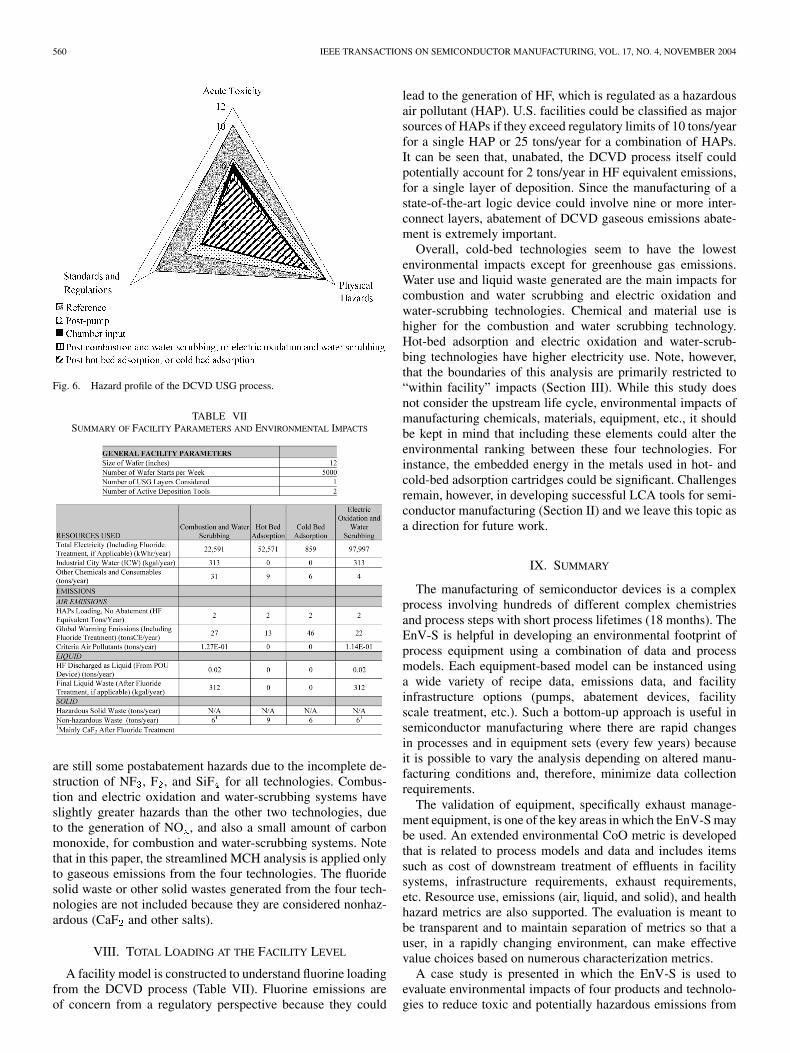
560 IEEE TRANSACTIONS ON SEMICONDUCTOR MANUFACTURING, VOL. 17, NO. 4, NOVEMBER 2004
Fig. 6. Hazard profile of the DCVD USG process.
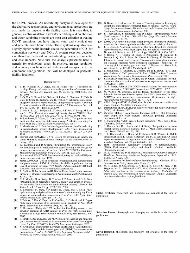
TABLE VIISUMMARY OF FACILITY PARAMETERS AND ENVIRONMENTAL IMPACTS
are still some postabatement hazards due to the incomplete de-struction of NF , F , and SiF for all technologies. Combus-tion and electric oxidation and water-scrubbing systems haveslightly greater hazards than the other two technologies, dueto the generation of NO , and also a small amount of carbonmonoxide, for combustion and water-scrubbing systems. Notethat in this paper, the streamlined MCH analysis is applied onlyto gaseous emissions from the four technologies. The fluoridesolid waste or other solid wastes generated from the four tech-nologies are not included because they are considered nonhaz-ardous (CaF and other salts).
VIII. TOTAL LOADING AT THE FACILITY LEVEL
A facility model is constructed to understand fluorine loadingfrom the DCVD process (Table VII). Fluorine emissions areof concern from a regulatory perspective because they could
lead to the generation of HF, which is regulated as a hazardousair pollutant (HAP). U.S. facilities could be classified as majorsources of HAPs if they exceed regulatory limits of 10 tons/yearfor a single HAP or 25 tons/year for a combination of HAPs.It can be seen that, unabated, the DCVD process itself couldpotentially account for 2 tons/year in HF equivalent emissions,for a single layer of deposition. Since the manufacturing of astate-of-the-art logic device could involve nine or more inter-connect layers, abatement of DCVD gaseous emissions abate-ment is extremely important.
Overall, cold-bed technologies seem to have the lowestenvironmental impacts except for greenhouse gas emissions.Water use and liquid waste generated are the main impacts forcombustion and water scrubbing and electric oxidation andwater-scrubbing technologies. Chemical and material use ishigher for the combustion and water scrubbing technology.Hot-bed adsorption and electric oxidation and water-scrub-bing technologies have higher electricity use. Note, however,that the boundaries of this analysis are primarily restricted to“within facility” impacts (Section III). While this study doesnot consider the upstream life cycle, environmental impacts ofmanufacturing chemicals, materials, equipment, etc., it shouldbe kept in mind that including these elements could alter theenvironmental ranking between these four technologies. Forinstance, the embedded energy in the metals used in hot- andcold-bed adsorption cartridges could be significant. Challengesremain, however, in developing successful LCA tools for semi-conductor manufacturing (Section II) and we leave this topic asa direction for future work.
IX. SUMMARY
The manufacturing of semiconductor devices is a complexprocess involving hundreds of different complex chemistriesand process steps with short process lifetimes (18 months). TheEnV-S is helpful in developing an environmental footprint ofprocess equipment using a combination of data and processmodels. Each equipment-based model can be instanced usinga wide variety of recipe data, emissions data, and facilityinfrastructure options (pumps, abatement devices, facilityscale treatment, etc.). Such a bottom-up approach is useful insemiconductor manufacturing where there are rapid changesin processes and in equipment sets (every few years) becauseit is possible to vary the analysis depending on altered manu-facturing conditions and, therefore, minimize data collectionrequirements.
The validation of equipment, specifically exhaust manage-ment equipment, is one of the key areas in which the EnV-S maybe used. An extended environmental CoO metric is developedthat is related to process models and data and includes itemssuch as cost of downstream treatment of effluents in facilitysystems, infrastructure requirements, exhaust requirements,etc. Resource use, emissions (air, liquid, and solid), and healthhazard metrics are also supported. The evaluation is meant tobe transparent and to maintain separation of metrics so that auser, in a rapidly changing environment, can make effectivevalue choices based on numerous characterization metrics.
A case study is presented in which the EnV-S is used toevaluate environmental impacts of four products and technolo-gies to reduce toxic and potentially hazardous emissions from
KRISHNAN et al.: QUANTIFYING ENVIRONMENTAL FOOTPRINT OF SEMICONDUCTOR EQUIPMENT USING ENVIRONMENTAL VALUE SYSTEMS 561
the DCVD process. An uncertainty analysis is developed forthe alternative technologies, and environmental projections arealso made for impacts at the facility scale. It is seen that, ingeneral, electric oxidation and water scrubbing and combustionand water-scrubbing systems are most cost effective at treatingDCVD emissions, but have higher water and chemical useand generate more liquid waste. These systems may also haveslightly higher health hazards due to the generation of CO (forcombustion systems) and NO . A system selection decisioncan, therefore, be based on understanding these environmentaland cost impacts. Note that the analysis presented here isgeneric for technology types. In practice, greater resolutionand accuracy can be obtained if data used are specific to theequipment configurations that will be deployed in particularfacility locations.
REFERENCES
[1] E. D. Williams, R. U. Ayres, and M. Heller, “The 1.7 kilogram mi-crochip: Energy and material use in the production of semiconductordevices,” Environ. Sci. Technol., vol. 36, no. 24, pp. 5504–5510, Dec.15, 2002.
[2] L.-Q. Xia, S. Nemani, M. Galiano, S. Pichai, S. Chandran, E. Yieh, D.Cote, R. Conti, D. Restaino, and D. Tobben, “High temperature subat-mospheric chemical vapor deposited undoped silicate glass: A solutionfor next generation shallow trench isolation,” J. Electrochem. Soc., vol.146, no. 3, pp. 1181–1185, Mar. 1999.
[3] L. Wei, Z. Z. Jia, J. Sudijuno, L. Y. Hoon, S. F. Kok, C. Leong, M. Liao,and S. L. Yih, “Characterization of high density plasma CVD USG film,”in Proc. SPIE—Int. Soc. Opt. Eng., vol. 3214, 1997, pp. 94–103.
[4] W. Lashbrook, P. O’Hara, D. Dance, and A. Veltri, “Design for environ-ment tools for management decision making: A selected case study,” inProc. IEEE Int. Symp. Electronics Environment, 1997.
[5] L. Mendicino and L. Beu, “Addressing environment, health, and safetyin semiconductor process development,” IEEE Trans. Components,Packaging Manufact. Technol., pt. C, vol. 21, no. 3, pp. 233–237, July1998.
[6] International SEMATECH, S70: Design for environment, safety, andhealth (DFESH) implementation strategy for the semiconductor in-dustry, 1995.
[7] W. Lashbrook and P. O’Hara, “Evaluating the environment, safetyand health impacts of semiconductor manufacturing at the design andprocess development stages,” in Proc. 19th IEEE/CPMT Int. ElectronicsManufacturing Technology Symp., Oct. 1996, pp. 232–236.
[8] International SEMATECH, Environmental, safety and health (ESH) costmodel development Rep., 1997.
[9] SEMI. (2003, Oct.) Cost of ownership for semiconductor manufacturingequipment metrics, E35-95A. [Online]. Available: http://www.semi.org
[10] Cost of ownership software. WWK Wright Williams and Kelley [Online].Available: http://www.wwk.com/home/solutions.asp
[11] R. Galli, A. H. Bachmann, and H. Binder, Reduction of production coststhroughE efficiency engineering, in Semiconduct. Fabtech, 8th ed., pp.85–90, 1998.
[12] C. F. Murphy, G. A. Kenig, D. T. Allen, J. P. Laurent, and D. E. Dyer,“Development of parametric material, energy, and emission invento-ries for wafer fabrication in the semiconductor industry,” Environ. Sci.Technol., vol. 37, no. 23, pp. 5373–5382, 2003.
[13] K. Schischke, M. Stutz, J. P. Ruelle, H. Griese, and H. Reichl, “Lifecycle inventory analysis and identification of environmentally significantaspects in semiconductor manufacturing,” in Proc. IEEE Symp. Elec-tronics Environment, 2001, pp. 145–150.
[14] F. Taiariol, P. Fea, C. Papuzza, R. Casalino, E. Galbiati, and S. Zappa,“Life cycle assessment of an integrated circuit product,” in Proc. IEEESymp. Electronics Environment, 2001, pp. 128–133.
[15] S. Hermanns, “Using the LCA method for identifying resource con-servation priorities at AMD saxony,” in Proc. NSF/SRC Center Envi-ronmentally Benign Semiconductor Manufacturing Tele-Seminar, Nov.2002.
[16] R. Smati, S. Raoux, D. Ho, and M. Woolston, “Measuring and modelinggas consumption and emissions from semiconductor manufacturing pro-cesses,” in Proc. SEMICON West EHS Assessment Techniques, 2002.
[17] N. Krishnan, S. Thurwachter, T. Francis, and P. Sheng, “A modular envi-ronmental design and decision-support tool (EDDT) for semiconductormanufacturing,” in Proc. SEMICON West Improving Environmental Per-formance of Wafer Manufacturing Processes, 2000.
[18] D. Bauer, N. Krishnan, and T. Francis, “Creating win-win: Leveraginginsight into industrial environmental decision-making,” in Proc. 4th Int.Symp. Environmental Issues With Materials and Processes for the Elec-tronics and Semiconductor Industries, 2001.
[19] S. Thurwachter, J. Schoening, and P. Sheng, “Environmental Value(EnV) analysis,” in Proc. 1999 IEEE Int. Symp. Electronics Environ-ment, 1999, pp. 70–75.
[20] (2003, Oct.) Applied materials silicon products information. [Online].Available: http://www.appliedmaterials.com/products/hdp_cvd.html
[21] J. E. Crowell, “Chemical methods of thin film deposition: Chemicalvapor deposition, atomic layer deposition, and related technologies,” J.Vacuum Sci. Technol., vol. A 21, no. 5, pp. S88–S95, Sept./Oct. 2003.
[22] S. Raoux, A. T. Tanaka, M. Bhan, H. Ponnekanti, M. Seamens, T.Deacon, L.-Q. Xia, F. Pham, D. Silvetti, D. Cheung, K. Fairbairn, A.Johnson, R. Pearce, and J. Langan, “Remote microwave plasma sourcefor cleaning chemical vapor deposition chambers: Technology forreducing global warming gas emissions,” J. Vacuum Sci. Technol. B,vol. 17, no. 2, pp. 477–485, March/April 1999.
[23] L. Mendicino, V. Vartanian, B. Goolsby, and P. T. Brown, “EHS anal-ysis of advanced CVD processes,” in Proc. SEMICON West TreatmentTechnologies for Emerging Semiconductor Processes, July 2001.
[24] J. Meyers, P. Maroulis, B. Reagan, and D. Green, Guidelines for envi-ronmental characterization of semiconductor equipment, InternationalSEMATECH, 2001.
[25] M. J. Sherer, Point-of-Use (POU) control systems for semiconductorprocess emissions (ESHC003), International SEMATECH, 1997.
[26] M. Waltrip, M. Czerniak, and D. Baker, “Evaluation of the BOCEdwards thermal conditioning system for HAP’s abatement,” in Proc.SEMICON West Improving Environmental Performance of WaferManufacturing Processes, 2000, pp. A-1–A-4.
[27] ATMI Novapure EGS237. (2003, Oct.) Dry bed abatement specificationsheet. [Online]. Available: www.atmi.com
[28] International SEMATECH, Fab utility cost values for cost of ownership(COO) calculations, 2002.
[29] Carnegie Mellon Green Design Initiative. (2003, Feb.) Economicinput output life cycle analysis (EIOLCA). [Online]. Available:http://www.eiolca.net
[30] S. Thurwachter, “Multi-criteria hazard evaluation,” M.S. thesis, Univ.California, Berkeley, 1998.
[31] S. Thurwachter, D. J. Bauer, and P. S. Sheng, “Integration of environ-mental factors in surface planning: Part 2—Multi-criteria hazard con-trol,” Trans. NAMRI, vol. 26, 1998.
[32] S. K. Hammond, C. J. Hines, M. F. Hallock, S. R. Woskie, S. Abdol-lahzadeh, R. Iden, E. Anson, F. Ramsey, and M. B. Schenker, “A tieredexposure-assessment strategy in the semiconductor health study,” Amer.J. Indust. Medicine, vol. 28, pp. 661–680, 1995.
[33] ITRS (International Technology Roadmap for Semiconductors).(2001) Environmental safety and health. [Online]. Available:http://public.itrs.net
[34] M. E. Williams and D. E. Baldwin, Semiconductor Industrial HygieneHandbook: Monitoring, Ventilation, Equipment and Ergonomics. ParkRidge, NJ: Noyes, 1995.
[35] Risk Assessment for Semiconductor Manufacturing. Cheshire, U.K.:Semiconductor Safety Association (Europe), 1999.
[36] M. P. Cullen, H. Checkoway, E. A. Eisen, K. Kelsey, C. Rice, D. H.Wegman, and L. Whitehead. (2001, Oct.) Cancer risk among waferfabrication workers in the semiconductor industry: Evaluation ofexisting data and recommended future research [Online]. Available:http://www.sia-online.org/pre_health.cfm
Nikhil Krishnan, photograph and biography not available at the time ofpublication.
Sebastién Raoux, photograph and biography not available at the time ofpublication.
David Dornfeld, photograph and biography not available at the time ofpublication.