Pronounced photovoltaic response from PN-junctions of multi-layered MoSe $ _2 $ on $ h $-BN
20
Pronounced photovoltaic response from PN-junctions of multi-layered MoSe 2 on h-BN Nihar R. Pradhan 1,ϯ , Shahriar Memaran 1,ϯ , Zhengguang Lu 1 , Daniel Rhodes 1 , Jonathan Ludwig 1 , Qiong Zhou 1 , Pulickel Ajayan 2 , Dmitry Smirnov 1 & Luis Balicas 1,* Several transition metal dichalcogenides (TMDs) such as MoS 2 , WSe 2 , etc., are semiconducting van der Waals bonded solids which are exfoliable down to single atomic layers 1,2 . Monolayers display unique optical 3,4,5 as well as optoelectronic properties, 6,7 while heterostructures incorporating graphene and multi-layered TMDs display pronounced photoconducting 8 and photovoltaic responses 9 . Rectification and the photovoltaic-effect was also reported for lateral 10,11 and for vertical PN-junctions composed respectively of a WSe 2 monolayer or a stack of WSe 2 /MoS 2 monolayers 12,13 . Here, we report the observation of rectification and enhanced photoconducting as well as photovoltaic, in lateral PN junctions based on multi-layered ambipolar 14 MoSe 2 crystals stacked onto h-BN. Our PN junctions composed of ~ 10 atomic layers are translucent enough to yield photoresponsitivities of 1 A/W, external quantum efficiencies exceeding 30 %, short circuit currents exceeding 10 3 A/cm 2 , and photovoltaic efficiencies surpassing 5 % with fill factors of ~ 70%. These values compare favourably with those of transparent photovoltaic cells 15,16,17 . Given that TMDs can be grown in large area, that their band gap(s) can be tuned by varying composition, and the available strategies for increasing their efficiency, e.g. the use of transparent graphene for contacts and gates 8,9 or the incorporation of plasmonic nanoparticles 18 , our results suggest a remarkable potential for semi-transparent photovoltaic cells composed of just a few layers of TMDs. 1 National High Magnetic Field Laboratory, Florida State University, Tallahassee-FL 32310, USA, 2 Department of Mechanical Engineering and Materials Science Rice University, Houston, TX 77005-1892, USA. ϯ These authors contributed equally to this work. * e-mail: [email protected]
Transcript of Pronounced photovoltaic response from PN-junctions of multi-layered MoSe $ _2 $ on $ h $-BN

Pronounced photovoltaic response from PN-junctions of multi-layered MoSe2 on h-BN
Nihar R. Pradhan1,ϯ, Shahriar Memaran1,ϯ, Zhengguang Lu1, Daniel Rhodes1, Jonathan
Ludwig1, Qiong Zhou1, Pulickel Ajayan2, Dmitry Smirnov1 & Luis Balicas1,*
Several transition metal dichalcogenides (TMDs) such as MoS2, WSe2, etc., are
semiconducting van der Waals bonded solids which are exfoliable down to single
atomic layers1,2. Monolayers display unique optical3,4,5 as well as optoelectronic
properties,6,7 while heterostructures incorporating graphene and multi-layered
TMDs display pronounced photoconducting8 and photovoltaic responses9.
Rectification and the photovoltaic-effect was also reported for lateral10,11 and for
vertical PN-junctions composed respectively of a WSe2 monolayer or a stack of
WSe2/MoS2 monolayers12,13. Here, we report the observation of rectification and
enhanced photoconducting as well as photovoltaic, in lateral PN junctions based on
multi-layered ambipolar14 MoSe2 crystals stacked onto h-BN. Our PN junctions
composed of ~ 10 atomic layers are translucent enough to yield
photoresponsitivities of 1 A/W, external quantum efficiencies exceeding 30 %,
short circuit currents exceeding 103 A/cm2, and photovoltaic efficiencies surpassing
5 % with fill factors of ~ 70%. These values compare favourably with those of
transparent photovoltaic cells15,16,17. Given that TMDs can be grown in large area,
that their band gap(s) can be tuned by varying composition, and the available
strategies for increasing their efficiency, e.g. the use of transparent graphene for
contacts and gates8,9 or the incorporation of plasmonic nanoparticles18, our results
suggest a remarkable potential for semi-transparent photovoltaic cells composed
of just a few layers of TMDs.
1National High Magnetic Field Laboratory, Florida State University, Tallahassee-FL 32310, USA, 2Department of Mechanical Engineering and Materials Science Rice University, Houston, TX 77005-1892, USA. ϯThese authors contributed equally to this work.*e-mail: [email protected]
2
The photovoltaic-effect (PE), or the creation of a voltage or an electrical current
in a given material or a solution upon light exposure, was discovered by Becquerel19 in
1839, although effective energy harvest from sunlight only became possible in the
1950’s with the advent of the silicon p−n junctions20. PN junctions, or adjacent hole-
and electron-doped semiconducting regions having a charge-carriers depleted interface,
are fundamental building blocks for today’s electronics and optoelectronics whose
fundamental technology still is based on Si despite recent progress in, for example,
perovskite solar cells21-23.
It was recently shown8-13 that it is possible to observe the photovoltaic effect in
photodiodes based on either lateral PN junctions10-11, or in heterostructures8,9,12,13 built
from atomically thin van der Waals materials, e.g. TMDs in combination with graphene,
which in contrast to Si are inherently flexible, semi-transparent, and lack interfacial
dangling bonds which, as argued in Ref.12, would allow the creation of high-quality
heterointerfaces without the constraint of atomically precise commensurability. The
availability of thin or single atomic layers of TMDs with distinct band gaps2,24 and work
functions provides the ability of i) engineering the band gaps in heterostructures, and ii)
fabricating photovoltaic cells composed simultaneously by TMDs with distinct gaps
absorbing either in the ultraviolet (e.g. thin HfS2) or infrared (e.g. WSe2, MoSe2, or
MoTe2) regions of the electromagnetic spectrum to create nearly transparent cells.
For lateral PN junctions based on a single atomic layer of WSe2, Ref.10 reports
maximum photovoltaic (or short-circuit) current densities jsc ~ 0.23 A/cm2 (for white
light illumination with a power density p = 3 x 10³ W/m2), with presumably a
photovoltaic efficiency η = Pel/P ≅ 0.5 % (where Pel is the photo-generated electrical
power and P is the illumination power). These values contrast to Ref.11 which reports jsc
≅ 150 A/cm2 (albeit for p ≅ 3.2 x 10⁶ W/m2 and λ = 700 nm) with external quantum
efficiencies (EQE or number of photo-generated carriers circulating through any given
photodetector per adsorbed photon and per unit time) in the order of just 10-3,

3
respectively. Owing to their direct semiconducting gap3 these single-atomic layer lateral
PN junctions also display electroluminescence suggesting their potential for
applications as light emitting diodes. Notice that despite the insofar small photovoltaic
efficiencies, these current densities surpass those of conventional PN junctions,
typically ~35 mA/cm2.
For vertical heterojunctions composed of single atomic layers of MoS2 (n-
doped) and WSe2 (p-doped or ambipolar) Ref.12 reports maximum jsc values
approaching 1 mA/cm2 (for p = 1 x 10⁶ W/m2 and λ = 532 nm). In contrast, Ref. 13
reports jsc ≅ 13 mA/cm2 with η ≅ 0.2 % (for white light illumination). For muti-layered
stacks of MoS2 and WSe2 contacted with graphene Ref.12 reports a much higher jsc value
of ~ 2.2 A/cm2 with EQE ≅ 34%. Furthermore, for a vertical heterostructure composed
of either a single or dual graphene electrodes, in combination with multilayered MoS2,
Ref.9 reports even larger jsc values i.e. ranging from 5 x 10² to ~ 1 x 10³ A/cm2, with
EQEs surpassing 25 %. These observations clearly indicate that PN junctions composed
of multi-layered TMDs can yield considerably higher photovoltaic currents and hence
ought to yield higher photovoltaic efficiencies.
Here, to evaluate this hypothesis, we fabricated lateral PN junctions (see Fig. 1)
composed of two lateral Au on Ti electrical gates evaporated onto SiO2, on top of
which, and as our choice for the gate dielectric, we transferred mechanically exfoliated
commercial h-BN (with a typical thickness t ≅ 40 nm). As a subsequent step, we
transferred25 a chemical vapor transport synthesized MoSe2 crystal, previously found by
us to display ambipolar behavior14, or the ability to accumulate either electrons or holes
at the interface with the dielectric material. Remarkably, we find that few atomic layer
ambipolar MoSe2 crystals display a photovoltaic response, even in the absence of gate
voltages or when not gated into a PN configuration. On SiO2 substrates this
photovoltaic response is observed to scale with the applied illumination power and the
gate voltage, leading to a diode like-response even in single gated transistors. A linear,

4
or ohmic-like, response as a function of excitation voltage is recovered when both the
illumination power and the gate voltage are removed. This suggests that the photo
generated electrons and holes would accumulate on different atomic layers, respectively
at the interfacial and at top layer due to the gate electric field, thus creating an effective
vertical PN junction. Furthermore, when multi-layered MoSe2 is placed on h-BN to
construct a double gated PN configuration, the resulting photodiode is found to exhibit a
remarkable photovoltaic response, with short circuit current densities exceeding 103
A/cm2, photovoltaic conversion efficiencies exceeding 5 % percent, and fill factors
approaching 70 %. These photovoltaic efficiencies are likely to increase, e.g. by
changing the materials used for, and the geometry of, the contacts and/or gates or by
incorporating plasmonic nanoparticles18, or just by optimizing the number of atomic
layers in order to maximize its interaction with light. Hence, given their relative
transparency in the visible region, e.g. a transmittance of ~ 74 % for a ~ 60 nm thick
MoS2 crystal26, as well as the ability to grow large areas27, few layer transition metal
dichalcogenides might lead to a new paradigm concerning transparent photovoltaics.
Figure 1a shows a photomicrography of one of our typical MoSe2 on h-BN
lateral PN junctions. As seen, the MoSe2 crystal is perceptible, but is transparent enough
to allow the visualization of both back gates through the h-BN crystal whose thickness
was determined to be ~ 45 nm through atomic force microscopy (AFM). The light
transmittance of the entire stack can be increased by using thinner crystals and by using,
for example, graphene for both back gates and for the electrodes on a transparent
substrate. Figure 1b shows a schematic of the measurements, where three independent
voltages, are applied to the sample, respectively Vbg1 for the left back-gate, Vbg2 for the
right one, excitation voltage Vds through source and drain contacts, measuring the
resulting drain to source current Ids under or without illumination. Figure 1c shows an
AFM image of the MoSe2 crystal. The red line indicates the line along which the height

5
profile shown in Fig. 1d was collected, which divided by an inter-layer spacing28 of
6.4655 Å indicates a crystal composed of 10 to 11 atomic layers.
Figure 1| Micrograph, measurement scheme, and thickness of a typical multilayered MoSe2 PN junction. a Micrograph of a multi-layered MoSe2 crystal stacked onto a ~ 25 nm thick h-BN crystal, itself placed onto a double gate structure patterned onto a SiO2/p-Si substrate. A thin red dotted line is used to delineate the MoSe2 crystal. The channel length (in between both voltage leads at either side of the junction) is l =5.52 µm and its average width w = 6.85 µm. The gap between gates is ~ 400 nm. b Configuration of measurements showing drain (D) and source (S) contacts, excitation voltage Vds, extracted source to drain current Ids, as well as the voltages applied to each back-gate, Vbg1 and Vbg2, respectively. Contacts and gates are composed of 50 nm of Au deposited onto a 5 nm thick layer of Ti. c Atomic force microscopy (AFM) image of the MoSe2 crystal on the SiO2 substrate. Red line depicts the line along which the height profile shown in d was collected. d Height profile of the mechanically exfoliated MoSe2 crystal showing the number of layers n = h/c’, where h is the height of the flake and c’= c/2 = 6.4655 Å is the inter-layer separation (c is the lattice constant along the inter-planar direction28).
Figure 2a displays drain to source current Ids as a function of the excitation
voltage Vds, when 20 V is applied to both gates but with opposite polarity. As expected

6
for a PN junction, and as previously reported for single-layer WSe2 heterostructures10,11,
our heterostructure composed of multi-layered MoSe2 displays rectification or a diode-
like response with the sign of the current depending on the gate voltage profile across
the junction. Figure 2b shows Ids as a function of Vds when either +20 or -20 V is
simultaneously applied to both gates. As seen, the diode-like response is no longer
observed, discarding a prominent role for the contacts and concomitant Schottky
barriers in relation to the aforementioned diode response. Figure 2c shows the same data
in a, but in a logarithmic scale. Fits of the observed diode response to the Shockley
equation in the presence of a series resistor29:
000
0 exp IfV
RIVfV
RIWRfVI
T
s
T
s
s
Tds −
+= (1)
where W is the Lambert function and VT the thermal voltage, yields ideality factors f
ranging between 1.6 and 1.8 with values for the series resistance Rs ranging from 1 to
2.5 MΩ. These f values are smaller or comparable to those in Refs.10,11 (1.9 ≤ f ≤ 2.6)
for single layered WSe2 lateral diodes. In any case, the Shockley-Read-Hall
recombination theory30,31, which assumes recombination via isolated point defect levels,
predicts f ≤ 2. Figure 2d displays Ids as a function of the gate voltage Vbg2 while Vbg1 is
maintained at a fixed value of +20 V (dark cyan trace) and -20 V (blue trace),
respectively. As seen, a sizeable drain to source current is observed only when both gate
voltages have the same polarity, i.e. resulting from the electric-field induced
accumulation of the same type of charge carriers. The resulting sub-threshold swing is
considerably sharper, i.e. ~ 380 mV per decade than the values extracted by us14 for
MoSe2 on SiO2. The same observation applies to the threshold gate voltage for
conduction, which is also nearly one order of magnitude smaller in the present case or
between 1 and 2 V. Both observations indicate that h-BN is a less disordered substrate
than SiO2. Finally, Figs. 2e and 2f display contour plots of the logarithm of the drain to
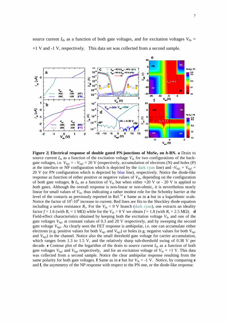
7
source current Ids as a function of both gate voltages, and for excitation voltages Vds =
+1 V and -1 V, respectively. This data set was collected from a second sample.
f
e
d
c
b
a
Figure 2| Electrical response of double gated PN-junctions of MoSe2 on h-BN. a Drain to source current Ids as a function of the excitation voltage Vds for two configurations of the back-gate voltages, i.e. Vbg1 = - Vbg2 = 20 V (respectively, accumulation of electrons (N) and holes (P) at the interface or NP configuration which is depicted by the dark cyan line) and -Vbg1 = Vbg2 = 20 V (or PN configuration which is depicted by blue line), respectively. Notice the diode-like response as function of either positive or negative values of Vds, depending on the configuration of both gate voltages. b Ids as a function of Vds but when either +20 V or - 20 V is applied to both gates. Although the overall response is non-linear or non-ohmic, it is nevertheless nearly linear for small values of Vds, thus indicating a rather modest role for the Schottky barrier at the level of the contacts as previously reported in Ref.14 c Same as in a but in a logarithmic scale. Notice the factor of 105-106 increase in current. Red lines are fits to the Shockley diode equation including a series resistance Rs. For the Vds < 0 V branch (dark cyan), one extracts an ideality factor f = 1.6 (with Rs = 1 MΩ) while for the Vds > 0 V we obtain f = 1.8 (with Rs = 2.5 MΩ). d Field-effect characteristics obtained by keeping both the excitation voltage Vds and one of the gate voltages Vbg1 at constant values of 0.3 and 20 V respectively, and by sweeping the second gate voltage Vbg2. As clearly seen the FET response is ambipolar, i.e. one can accumulate either electrons (e.g. positive values for both Vbg1 and Vbg2) or holes (e.g. negative values for both Vbg1 and Vbg2) in the channel. Notice also the small threshold gate voltage for carrier accumulation, which ranges from 1.3 to 1.5 V, and the relatively sharp sub-threshold swing of 0.38 V per decade. e Contour plot of the logarithm of the drain to source current Ids as a function of both gate voltages Vbg1 and Vbg2 respectively, and for an excitation voltage of Vds = +1 V. This data was collected from a second sample. Notice the clear ambipolar response resulting from the same polarity for both gate voltages. f Same as in e but for Vds = -1 V. Notice, by comparing e and f, the asymmetry of the NP response with respect to the PN one, or the diode-like response.

8
The colour code is such that our noise floor, i.e. currents between 10-12 and 10-11 A,
corresponds to the red regions in both plots. Currents ranging from ~ 0.1 to 1 µA are
depicted by the clear blue and darker blue regions, respectively. Although both panels
are not similarly asymmetric, it is clear that a sizeable current is obtained when both
gates are simultaneously energized with the same polarity leading to charge
accumulation due to the field-effect. However, due to the rectification-effect, both
figures become asymmetric when both gates are energized with opposite polarities:
sizeable currents are observed in the second and fourth quadrants in Figs. 2e and 2f,
respectively.
In figure 3 we evaluate the photo-response of multi-layered MoSe2 on h-BN in
absence of gate voltages. Figure 3a displays the generated photocurrent Iph = Ids (P) – Ids
(P = 0 W) as a function of the excitation voltage Vds for several values of the applied
laser power P with a spot size = 3.5 µm (see Methods) and for λ = 532 nm. Notice i) the
sizeable photo-generated current and ii) the emergence of a finite short-circuit current
(Ids(Vds = 0 V)) resulting from the photovoltaic-effect. This indicates i) that the photo-
generated electron-hole pairs have a long enough diffusion length to reach the electrical
contacts and ii) the existence of a built-in electric-field which drives the photo-
generated carriers towards the contacts. This electric-field might result from slightly
asymmetric Schottky barriers at the contacts which pins the Fermi-level at distinct
positions with respect to the valence band maximum at each contact, thus creating a
gradient of chemical potential. In addition, it is quite likely that the charge distribution
at the MoSe2/h-BN interface is inhomogeneous, with the largest charge-density located
immediately below the laser spot. This inhomogeneous charge distribution would create
an effective PN junction thus explaining both the photovoltaic response and the

9
asymmetric Ids as a function of Vds characteristics shown in Fig. 3 a. Figures 3b and c
show respectively, the photoresponsivity R = Iph/P and concomitant external quantum
efficiency EQE = hcIph/eλP, where h is the Planck constant, c the speed of light, and e
the electronic charge, from the data in a.
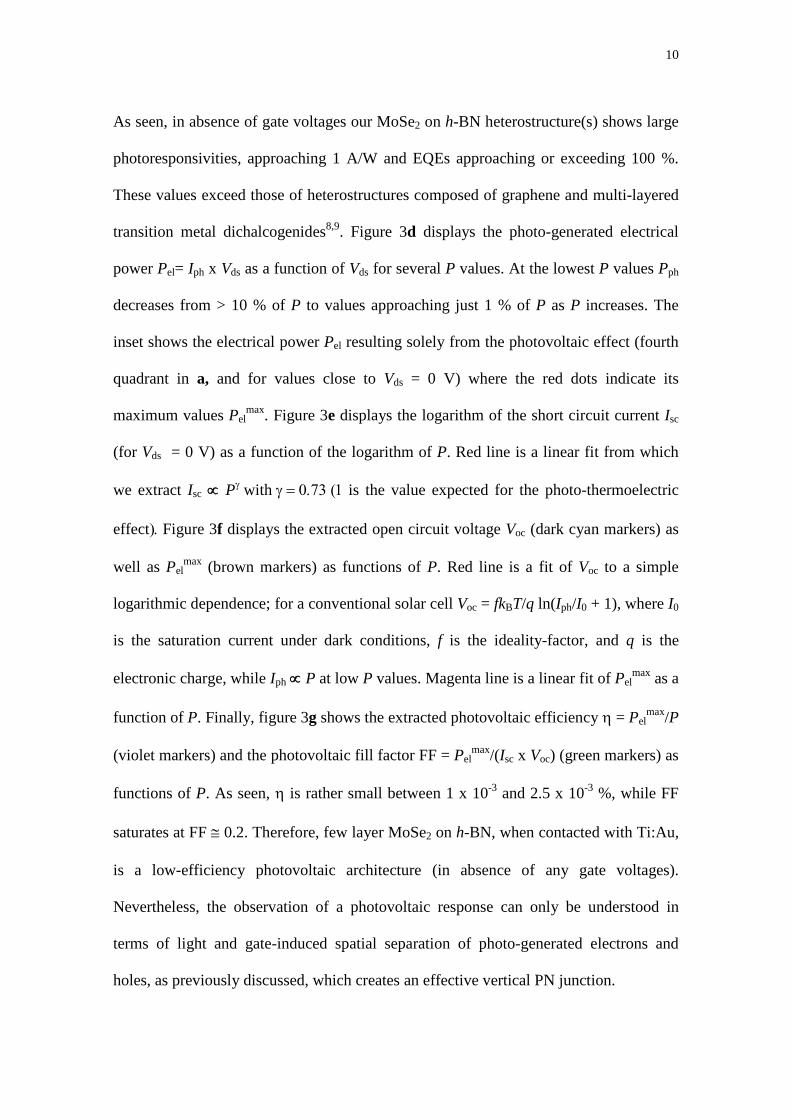
Figure 3| Photoconductivity, photovoltaic response, concomitant external quantum efficiencies, and photon generated electrical power in absence of gate-voltage(s). Photocurrent Iph = Ids (P) - Ids (P = 0), where P is the applied laser power (wavelength λ = 532 nm, spot size ~ 3.5 µm, see Methods), as a function of the excitation voltage Vds, for several values of P ranging from P = 0.04 to 30 µW and in the absence of gate voltage(s). Red square emphasizes the existence of a sizeable, power-dependent, photo-generated current Ipv for Vds = 0 V, or photovoltaic current. b From the curves in a, photoresponsivity R = Iph/P as a function of Vds. Notice the quite large values of R, approaching 1 A/W at the lower power P levels, but it decreases fast to values ranging from 100 mA/W to 250 mA/W as the power increases by one order of magnitude. c External quantum efficiencies from the Iph data in b, where h, c, e and λ are the Planck constant, speed of light, electronic charge and excitation wavelength, respectively. Notice that EQE ranges from 25 to ~ 200% at low power levels. d Electrical power Pel= Iph x Vds resulting from photon-generated electron-hole pairs as a function of Vds and for several laser P values. As seen, in absence of any gate voltage, a laser power P = 30 µW yields ~0.25 and ~0.36 µW of photo generated electrical power for Vds = -1 and +1 V, respectively. The color code is the same for all four panels: dark cyan trace corresponds to P = 0.04 µW, blue trace to P=0.16 µW, and so forth. Inset: photogenerated power in the vicinity of zero excitation voltage (in an amplified scale), where it is dominated by the photovoltaic effect. The peak corresponds to the maximum electrical power Pel
max (red markers) generated by the photovoltaic effect. e Short circuit current Isc, extracted from a when Vds = 0 V, as a function of the laser power P. Red line is a linear fit yielding Isc ∝ P1.3. f Open circuit voltage Voc (dark cyan markers), as extracted from a from the condition Iph = 0 A and maximum electrical power Pel
max from the inset in d, both as functions of P. Red line is a logarithmic fit. g Photovoltaic efficiency η = Pel
max/P (green markers) and fill factor FF = Pel max/ IscVoc (violet markers).
10
As seen, in absence of gate voltages our MoSe2 on h-BN heterostructure(s) shows large
photoresponsivities, approaching 1 A/W and EQEs approaching or exceeding 100 %.
These values exceed those of heterostructures composed of graphene and multi-layered
transition metal dichalcogenides8,9. Figure 3d displays the photo-generated electrical
power Pel= Iph x Vds as a function of Vds for several P values. At the lowest P values Pph
decreases from > 10 % of P to values approaching just 1 % of P as P increases. The
inset shows the electrical power Pel resulting solely from the photovoltaic effect (fourth
quadrant in a, and for values close to Vds = 0 V) where the red dots indicate its
maximum values Pelmax. Figure 3e displays the logarithm of the short circuit current Isc
(for Vds = 0 V) as a function of the logarithm of P. Red line is a linear fit from which
we extract Isc ∝ Pγ with γ = 0.73 (1 is the value expected for the photo-thermoelectric
effect). Figure 3f displays the extracted open circuit voltage Voc (dark cyan markers) as
well as Pelmax (brown markers) as functions of P. Red line is a fit of Voc to a simple
logarithmic dependence; for a conventional solar cell Voc = fkBT/q ln(Iph/I0 + 1), where I0
is the saturation current under dark conditions, f is the ideality-factor, and q is the
electronic charge, while Iph ∝ P at low P values. Magenta line is a linear fit of Pelmax as a
function of P. Finally, figure 3g shows the extracted photovoltaic efficiency η = Pelmax/P
(violet markers) and the photovoltaic fill factor FF = Pelmax/(Isc x Voc) (green markers) as
functions of P. As seen, η is rather small between 1 x 10⁻³ and 2.5 x 10⁻³ %, while FF
saturates at FF ≅ 0.2. Therefore, few layer MoSe2 on h-BN, when contacted with Ti:Au,
is a low-efficiency photovoltaic architecture (in absence of any gate voltages).
Nevertheless, the observation of a photovoltaic response can only be understood in
terms of light and gate-induced spatial separation of photo-generated electrons and
holes, as previously discussed, which creates an effective vertical PN junction.

11
Figure 4 on the other hand, describes the overall photo-electronic and
photovoltaic response when voltages are applied to the gate electrodes. In figure 4a we
plot the short circuit current Isc (or Ids for Vds = 0 V) as a function of Vj = Vbg1 = -Vbg2,
hence in rectification mode, for several values of the incident power P. As seen, and
although the response is asymmetric, one can extract very sizeable short circuit currents
(e.g. for Vj = -5V) ranging from 0.2 µA to 1.5 µA depending on the P level.

12
Figure 4| a Photovoltaic response: photoelectric generated power, efficiency and fill factor. Photovoltaic or short circuit current under illumination Isc (or Iph(Vds = 0 V)) as a function of the combined gate voltage Vj = Vbg1= - Vbg2 and for several values of P. As seen, under P = 30 µW and Vj = -5 V one extracts a very sizeable photovoltaic current of 1.5 µA, which renormalized by sample’s cross section translates into a current density of ~ 3 x 10³ A/cm2. b Photoresponsivity R as a function of Vj, from the curves in a. R displays the largest values at the smallest power values, e.g. ~ 1.4 A/W under P = 1.2 µW. c Concomitant EQE from the curves in b. Notice how it achieves values approaching ~ 30% at the lowest P value. d Ids as a function of Vds under Vj = 5 V (PN configuration) showing diode-like, or rectification response and for several values of the illumination power P. e Photo-generated electrical power Pel = Ids x Vds from the second quadrant (i.e. Ids > 0 and Vds < 0) in d. In d and in e the applied laser power P is indicated by the same line color code. Red dots indicate the maximum extracted photovoltaic power levels Pel
max. f Log-log plot of the photovoltaic or short-circuit current Isc as a function of the laser power density p for Vj = - 5 V, from the data in a (solid blue circles). The same graph displays data from a second PN junction composed of 13 atomic layers which was measured at lower power densities (open blue circles). Red line is a linear fit yielding jsc ∝ p0.85. g Open-circuit voltage Voc as extracted from the curves in d when Isc = 0 A and as a function of p (solid circles). The same graph contains data from the second sample (open circles). Red lines are logarithmic fits. h Maximum extracted photovoltaic output power or Pel
max from the curves in e (indicated by the red dots) as a function of the applied power density p. The Pel
max values extracted from samples 1 and 2 are indicated by solid and open circles, respectively. Red line is a linear fit yielding Pel
max ∝ p0.8. i Photovoltaic efficiency η = Pelmax / P for both samples
(magenta markers) and photovoltaic fill-factor FF = Pelmax / (Isc x Voc) (blue markers) as
functions of p. Solid and open circles depict results samples #1 and #2, respectively.
This translates into R values ranging from 40 to over 100 mA/W and concomitant
maximum EQEs ranging from ~10 to 30%. Figure 4d displays Ids as function of Vds,
under Vj = - 5 V for several power levels. Notice the sizeable photo-generated current,
particularly at high P levels, and at Vds = 0 V. Figure 4e, displays the concomitant Pel
associated with the photovoltaic effect (i.e. second quadrant in d) where red markers
indicate its maximum values Pelmax. Figures 4f displays the Isc values (renormalized by
the channel width and the crystal thickness) extracted from a for Vj = - 5 V, while Fig.
4g shows the Voc values extracted from d, both as functions of the power density p. In
both graphs, we also included data from a second sample (open circles) composed of 8.8
µm wide and ~13 atomic layers MoSe2 crystal, with both back-gates also excited at ±5
V. This crystal was measured under lower power levels. In Fig. 4f and g red lines are
linear (yielding jsc ∝ p0.85) and logarithmic fits, respectively. Notice the very high

13
current densities, ranging from ~ 5 A/cm2 and surpassing 103 A/cm2 at high power
levels. Notice also the large saturating values for Voc ≅ 0.8 V (sample #1) or 0.85 V
(sample #1). The typical room temperature values for high quality monocrystalline Si
solar cells range from jsc ≅ 28 to 46 mA/cm2 with Voc ~ 0.6 V, respectively. Figure 4h
displays Pelmax as a function of p (extracted from e, where it is indicated by red dots);
red line is a linear fit yielding Pelmax ∝ p0.8. Again open markers depict data from sample
#2. Since one naively assumes that the number of photo-generated excitons would be
linearly proportional to the applied power, this sub-linear dependence would perhaps
suggest certain prevalence for excitonic recombination mechanisms. Finally, Fig. 4i
shows the extracted η and FF values, yielding η values surpassing 5 % at lower p’s, and
peaking at values approaching 10 % as p increases. The observed peak most likely
results from a competition between the number of photo-generated carriers which is ∝ p
and exciton recombination mechanisms which become prevalent at higher power levels.
FF on the other hand, remains nearly constant at ~ 0.7, although in sample # 2 it
decreases to 0.5 at higher power levels.
In addition to the ability of producing extremely thin films (one or a few atomic
layers) over relatively large areas, our choice of MoSe2 as the semiconducting
compound in PN junction-like heterostructures is motivated by two other factors: i) the
size of its semiconducting gap32, i.e. an indirect gap of 1.41 eV (comparable to CdTe
and GaAs) in multi-layered crystals, and a direct gap of 1.58 eV in single atomic layers
which, according to the Shockley–Queisser limit33, would yield a maximum theoretical
photovoltaic efficiency for a single PN junction of η ~ 35%, and ii) the relative
abundance of the raw elements in MoSe2 in comparison to more conventional
photovoltaic semiconductors such as CdTe or CuInSe2. In effect, the earth’s crust

14
abundance for In, Te and Se are 160, 1 and 50 parts per billion respectively, and
although Se is not abundant, ultra-thin heterostructures, as studied here, would require
very small quantities of this element. Nevertheless, our most important result is the
observation of photovoltaic efficiencies surpassing 5 % at lower power densities which,
with improvements in contacts and in the geometry of PN junction, might one day
approach the theoretical limit η = 35 %. Notice that tandem junctions connected in
parallel or in series (for example, by stacking MoSe2 with other TMDs having quite
different band gaps such as HfS2 or MoTe2) are not subjected to this limit. Furthermore,
recent photovoltaic technologies, such as organic solar cells, have seen a steep increase
in efficiency within a few years34, suggesting that there are ample opportunities for
improvement in the efficiency/performance of TMDs based photovoltaic cells, with the
added advantage of flexibility and in particular light transmittance26, which would make
them ideal for covering large area windows or entire buildings.
References
1. Coleman, J. N. et al. Two-Dimensional Nanosheets Produced by Liquid
Exfoliation of Layered Materials. Science 331, 568-571 (2011).
2. Chhowalla, M.; Shin, H. S.; Eda, G.; Li, L. J.; Loh, K. P.; Zhang, H. The
chemistry of two-dimensional layered transition metal dichalcogenide
nanosheets. Nature Chem. 5, 263-275 (2013).
3. Mak, K. F., Lee, C., Hone, J., Shan, J. & Heinz, T. F. Atomically thin MoS2 A
new direct-gap semiconductor. Phys. Rev. Lett. 105, 136805 (2010).
4. Ross, J. S. et al. Electrical control of neutral and charged excitons in a
monolayer semiconductor. Nat. Commun. 4, 1474 (2013)

15
5. Jones, A. M. et al. Optical generation of excitonic valley coherence in
monolayer WSe2. Nature Nanotech. 8, 634-638 (2013)
6. Wang, Q. H.; Kalantar-Zadeh, K.; Kis, A.; Coleman, J. N. & Strano, M. S.
Electronics and optoelectronics of two-dimensional transition metal
dichalcogenides, Nature Nanotech. 7, 699-712 (2012).
7. Lopez-Sanchez, O.; Lembke, D.; Kayci, M.; Radenovic, A. & Kis, A.
Ultrasensitive photodetectors based on monolayer MoS2 Nature Nanotech. 8,
497-501 (2013).
8. Britnell, L. et al. Field-effect tunneling transistor based on vertical graphene
heterostructure. Science 340, 1311 (2013).
9. Yu, W. J. et al. Highly efficient gate-tunable photocurrent generation in vertical
heterostructures of layered material. Nature Nanotech. 8, 952-958 (2013).
10. Pospischil, A, Furchi, M. M., Mueller, T. Solar-energy conversion and light
emission in an atomic monolayer p-n diode. Nature Nanotech. 9, 257-261
(2014).
11. Baugher, B. W. H. , Churchill, H. O. H., Yang, Y. F., Jarillo-Herrero, P.
Optoelectronic devices based on electrically tunable p-n diodes in a monolayer
dichalcogenide. Nature Nanotech. 9, 262-267 (2014).
12. Lee, C.-H. et al. Atomically thin p–n junctions with van der Waals
Heterointerfaces. Nature Nanotech. 9, 676-681(2014).
13. Furchi, M. M.; Pospischil, A.; Libisch, F.; Burgdorfer J. & Mueller T.
Photovoltaic Effect in an Electrically Tunable van der Waals Heterojunction.
Nano Lett. 14, 4785-4790 (2014).

16
14. Pradhan, N. R. et al. Ambipolar Molybdenum Diselenide Field-Effect
Transistors: Field-Effect and Hall Mobilities. ACS Nano 8, 7923-7929 (2014).
15. Lunt, R. R. & Bulovic, V. Transparent, near-infrared organic photovoltaic solar
cells for window and energy-scavenging applications. Appl. Phys. Lett. 98,
113305 (2011).
16. Zhao, Y.; Meek, G. A.; Levine, B. G. & Lunt, R. R. Near-Infrared Harvesting
Transparent Luminescent Solar Concentrators. Adv. Opt. Mater. 2, 606–611.
(2014).
17. Chen, C.-C. et al. Visibly Transparent Polymer Solar Cells Produced by
Solution Processing. ACS Nano 6, 7185-7190 (2012).
18. Atwater, H. A. & Polman, A. Plasmonics for improved photovoltaic devices,
Nature Mater. 9, 205-2013 (2010).
19. Becquerel, E. Mémoire sur les effets électriques produits sous l'influence des
rayons solaires. Comptes Rendus 9, 561–567 (1839).
20. Chapin, D. M.; Fuller, C. S. & Pearson, G. L. J. A New Silicon p-n Junction
Photocell for Converting Solar Radiation into Electrical Power. Appl. Phys. 25,
676−677 (1954).
21. Lee, M. M.; Teuscher, J.; Miyasaka, T.; Murakami, T. N.; Snaith, H. J. Efficient
Hybrid Solar Cells Based on Meso-Superstructured Organometal Halide
Perovskites. Science 338, 643−647 (2012).
22. Grinberg, I. et al. Perovskite oxides for visible-light-absorbing ferroelectric and
photovoltaic materials. Nature 503, 509-512 (2013).
23. Liu, M.; Johnston, M. B. & Snaith, H. J. Efficient planar heterojunction
perovskite solar cells by vapour deposition. Nature 501, 395-398 (2013).

17
24. Tonndorf, P. et al. Opt. Express 21, 4908−4916 (2013).
25. Li, H. & et al. A Universal, Rapid Method for Clean Transfer of Nanostructures
onto Various Substrates, ACS Nano 8, 6563-6570 (2014).
26. Yoon J. & et al. Highly Flexible and Transparent Multilayer MoS2 Transistors
with Graphene Electrodes, Small 19, 3295-3300 (2013).
27. Wang, X. L. et al. Chemical Vapor Deposition Growth of Crystalline Mono
layer MoSe2, ACS Nano 8, 5125-5131 (2014).
28. James, P. B. & Lavic, M. T. The crystal structure of MoSe2, Acta Cryst. 16.
1183 (1963).
29. Banwell, T. & Jayakumar, A. Exact analytical solution for current flow through
diode with series resistance. Electron. Lett. 36, 291–292 (2000).
30. Shockley W. & Read, W. T. Statistics of the Recombinations of Holes and
Electrons. Phys. Rev. 87, 835 (1952).
31. Hall, R. N. Electron-hole Recombination in Germanium. Phys. Rev. 87, 387
(1952).
32. Zhang, Y. et al. Direct observation of the transition from indirect to direct
bandgap in atomically thin epitaxial MoSe2. Nature Nanotech. 9, 111-115
(2014).
33. Shockley W. & Queisser, H. J. Detailed Balance Limit of Efficiency of p-n
Junction Solar Cells. J. Appl. Phys. 32, 510-519 (1961).
34. Ameri, T.; Li, N. & Brabec C. J. Highly efficient organic tandem solar cells: a
follow up review. Energy Environ. Sci. 6, 2390 (2013).

18
Supplementary Materials
Methods
MoSe2 single crystals were synthesized through a chemical vapor transport technique
using either iodine or excess Se as the transport agent. 99.999% pure Mo powder and
99.999% pure Se pellets were introduced into a quartz tube together with 99.999% pure
iodine. The quartz tube was vacuumed, brought to 1150 oC, and held at this temperature
for 1.5 weeks at a temperature gradient of < 100 oC. Subsequently, it was cooled to
1050 oC at a rate of 10 oC per hour, followed by another cool down to 800 oC at a rate of
2 oC per hour. It was held at 800 oC for 2 days and subsequently quenched in air. Multi-
layered flakes of MoSe2 were exfoliated from these single crystals by using the
micromechanical cleavage technique, and transferred onto p-doped Si wafers covered
with a 270 nm thick layer of SiO2. h-BN crystals (Momentive PolarTherm PT110) were
mechanically exfoliated from larger crystals, and transferred onto pre-evaporated Ti:Au
gates, using a technique similar to the one described in Ref.25. The MoSe2 crystal was
subsequently transferred onto the h-BN crystal by using the same technique. For making
the gates and the electrical contacts 90 nm of Au was deposited onto a 4 nm thick layer
of Ti via e-beam evaporation. Contacts and gates were patterned by using standard e-
beam lithography techniques. After each transfer, as well as after the final gold
deposition, the samples are annealed at 200 0C for ~ 2 h in forming gas. After the
heterostructure is completed it is re-annealed under high vacuum for 24 hours at 120oC.
Atomic force microscopy (AFM) imaging was performed using the Asylum Research
MFP-3D AFM. Electrical characterization was performed by using a combination of
sourcemeter (Keithley 2612 A), coupled to a Physical Property Measurement System.
For photo-current measurements a Coherent Sapphire 532-150 CW CDRH and

19
Thorlabs DLS146-101S were used, with a continuous wavelength of 532 nm. Light was
transmitted to the sample through a 3 µm single-mode optical-fiber with a mode field
diameter of 3.5 µm. The size of the laser spot was measured against a fine grid. Hence,
here we use 3.5 µm for the laser spot diameter assuming a constant power density
distribution in order to approximate the Gaussian distribution corresponding to the
mode field diameter of 3.5 µm (see Supplementary Information). Particular care was
taken to avoid illumination of the electrical contacts. For the dark current
measurements, the device under test was covered with a black box (with controlled
access for the laser beam) to prevent any exposure to light.
Acknowledgements
We acknowledge Prof. P. Kim and Dr. C.-H. Lee for their guidance in developing our
crystal transfer and stacking technique(s). This work is supported by the U.S. Army
Research Office MURI grant W911NF-11-1-0362. ZL, JL and DS acknowledge the
U.S. Department of Energy, Office of Basic Energy (DE-FG02-07ER46451) for the
support for the photo-response measurements. The NHMFL is supported by NSF
through NSF-DMR-0084173 and the State of Florida.
Authors' Contributions
LB conceived the project in discussions with SM, NRP, DR, DS and PA. DR
synthesized the MoSe2 single crystals and developed micro-crystal transfer station and
technique upon the guidance of CHL and PK. NRP, SM and DR characterized the
thickness of the used flakes though AFM techniques. SM fabricated the PN junctions.
NRP, SM and QZ performed the electrical transport characterization. NRP, SM, ZL, JL,
QZ and DS performed the photo-response/photovoltaic measurements. NRP, SM, QZ

20
and LB analysed the corresponding data. LB wrote the manuscript with the input of all
co-authors.
Additional information
Supplementary information is available in the online version of the paper. Reprints and
permissions information is available online at www.nature.com/reprints.
Correspondence and requests for materials should be addressed to L.B.
Competing Interests statement
The authors declare that they have no competing financial interests.

![Enhancement of surface mechanical properties by using TiN[BCN/BN] n /cBN multilayer system](https://static.fdokumen.com/doc/165x107/631a181cbb40f9952b01d9ec/enhancement-of-surface-mechanical-properties-by-using-tinbcnbn-n-cbn-multilayer.jpg)