Product / Process Change Notification
83
DRAFT Important information for your attention: Product / Process Change Notification Dear Customer, please find attached our INFINEON Technologies PCN: Final PCN: Several changes affecting Gen 5P Mosfets for DSO8 package N° 2019-184-A2 ▪ Please respond to this PCN by indicating your decision on the approval form, sign it and return to your sales partner before 2021-04-15. ▪ Infineon aligns with the widely-recognized JEDEC STANDARD “JESD46“, which stipulates: “Lack of acknowledgement of the PCN within 30 days constitutes acceptance of the change.” Your prompt reply will help Infineon Technologies to assure a smooth and well-executed transition. If Infineon does not hear from your side by the due date, we will assume your full acceptance to this proposed change and its implementation. Your attention and response to this matter is greatly appreciated. Infineon Technologies AG Postal Address Headquarters: Am Campeon 1-15, D-85579 Neubiberg, Phone +49 (0)89 234-0 Chairman of the Supervisory Board: Dr. Wolfgang Eder Management Board: Dr. Reinhard Ploss (CEO), Dr. Helmut Gassel, Jochen Hanebeck, Dr. Sven Schneider Registered Office: Neubiberg Commercial Register: München HRB 126492 Notwithstanding the aforesaid individual agreements shall prevail. Page 1 of 3 2021-03-05 restricted
-
Upload
khangminh22 -
Category
Documents
-
view
5 -
download
0
Transcript of Product / Process Change Notification

DRAFT
Important information for your attention:
Product / Process
Change Notification
Dear Customer,
please find attached our INFINEON Technologies PCN:
Final PCN: Several changes affecting Gen 5P Mosfets for DSO8 package
N° 2019-184-A2
▪ Please respond to this PCN by indicating your decision on the approval form, sign it and return to your sales partner
before 2021-04-15.
▪ Infineon aligns with the widely-recognized JEDEC STANDARD “JESD46“, which stipulates:
“Lack of acknowledgement of the PCN within 30 days constitutes acceptance of the change.”
Your prompt reply will help Infineon Technologies to assure a smooth and well-executed transition. If Infineon does not hear
from your side by the due date, we will assume your full acceptance to this proposed change and its implementation.
Your attention and response to this matter is greatly appreciated.
Infineon Technologies AG
Postal Address Headquarters: Am Campeon 1-15, D-85579 Neubiberg, Phone +49 (0)89 234-0
Chairman of the Supervisory Board: Dr. Wolfgang Eder
Management Board: Dr. Reinhard Ploss (CEO), Dr. Helmut Gassel, Jochen Hanebeck, Dr. Sven Schneider
Registered Office: Neubiberg
Commercial Register: München HRB 126492
Notwithstanding the aforesaid individual agreements shall prevail.
Page 1 of 32021-03-05 restricted

DRAFT
Product / Process
Change Notification
N° 2019-184-A2
Products affected
Detailed Change Information
Subject:
Reason / Motivation:
Description Old New
PROCESS - WAFER PRODUCTION:
New / change of metallization
(specifically chip backside)
Cr/Ni/Ag Sputter Process Ti/Ni/Ag Evaporation Process
PROCESS - WAFER PRODUCTION:
New / change of metallization
(specifically chip frontside)
Al/Si Al/Si/Cu
PROCESS - WAFER PRODUCTION:
Move of all or part of wafer fab to a
different location/site/subcontractor
Infineon Technologies Americas Corp.,
Temecula, United StatesEPISIL Technologies Inc., Taiwan
PROCESS - ASSEMBLY:
Change of product markingSite location code"C"
Site location code"/P"-Except
AUIRF7397QTR
PROCESS - ASSEMBLY:
Move of all or part of assembly to a
different location/site/subcontractor.
Carsem (M) Sdn.Bhd., Malaysia Amkor Technology Malaysia Sdn. Bhd.,
Malaysia - Except AUIRF7397QTR
TEST FLOW:
Move of all or part of electrical wafer
test and/or final test to a different
location/site/subcontractor
Wafer Probe site: Infineon Technologies
Americas Corp., Temecula, United States
Final Test site; Carsem (M) Sdn.Bhd.
Wafer Probe site: EPISIL Technologies
Inc., Taiwan
Final Test site; Amkor Technology
Malaysia Sdn. Bhd., Malaysia - Except
AUIRF7397QTR
Product Identification
Please refer to attached affected product list 1_cip19184_A2
Final PCN: Several changes affecting Gen 5P Mosfets for DSO8 package
Production consolidation
Traceability assured via Lot number an date code. Assembly site code updated
Page 2 of 32021-03-05 restricted

DRAFT
Product / Process
Change Notification
N° 2019-184-A2
Anticipated Impact of Change
Attachments 1_cip19184_A2 affected product list
3_cip19184_A2 customer information package
Time Schedule
Final qualification report
First samples available
Intended start of delivery [1]
Last Order Date (LOD) [2]
Last Delivery Date (LDD) [3]
No expected impact on electrical performance. Quality and reliability verified by
qualification.
2021-02-28
2021-02-28
3/1/2021 upon approval
If you have any questions, please do not hesitate to contact your local Sales Office.
2021-04-30
2021-10-31
DeQuMa-ID(s): SEM-PW-06 / SEM-PW-07 / SEM-PW-13 / SEM-PA-13 / SEM-PA-
18 / SEM-TF-01
[1] Provided date or earlier after customer approval
[2] Last time buy volume to be placed latest until LOD
[3] Delivery of new product can be earlier (see Intended start of delivery) and depends on approval
Page 3 of 32021-03-05 restricted

PCN 19-184-A2Temecula Transfer G5P DSO8 Mosfet
January 14, 2021Confidential

Copyright © Infineon Technologies AG 2020. All rights reserved. 2
Agenda
Motivation of the change
PCN details
5M+1E Difference
5M+1E Difference Front End
Comparison of clean room level Front End (Environment)
Operator training system Front End (Man)
Equipment comparison Front End (Machine)
Structure comparison table & Materials Front End (Material)
1
2
3
4
5
6
7
8
2020-01-14 Confidential

Copyright © Infineon Technologies AG 2020. All rights reserved. 3
Agenda
Process flow comparison & Wafer shipping box Front End (Method)
Advanced Measurement System Analysis Front End (Measurement)
5M+1E Difference Back End
Comparison of clean room level Back End (Environment)
Operator training system Back End (Man)
Equipment comparison Back End (Machine)
Structure comparison table & Materials Back End (Material)
Process flow comparison & Wafer shipping box Back End (Method)
9
10
11
12
13
14
15
16
2020-01-14 Confidential

Copyright © Infineon Technologies AG 2020. All rights reserved. 4
Agenda
Final Test Comparison Parameter Results (Measurement)
Electrical Distribution Results
Qualification test report
17
18
19
2020-01-14 Confidential

Copyright © Infineon Technologies AG 2020. All rights reserved. 5
Agenda
Motivation of the change
PCN details
5M+1E Difference
5M+1E Difference Front End
Comparison of clean room level Front End (Environment)
Operator training system Front End (Man)
Equipment comparison Front End (Machine)
Structure comparison table & Materials Front End (Material)
1
2
3
4
5
6
7
8
2020-01-14 Confidential

Transfer to SiFo …
Transfer to SiFo
› Phase out Temecula frontend site
› Transfer to silicon foundries
62020-01-14 Confidential Copyright © Infineon Technologies AG 2020. All rights reserved.

Search for silicon foundries
Our decision: Phase out of 6 inch Temecula frontend site to silicon foundries
In the interest of best serving the needs of our customers and
continuing our path of profitable growth, Infineon has been assessing
the Temecula, California 6" wafer fab as part of the strategic analysis
of our global production landscape.
The site's comparatively low economies of scale have led to the
difficult decision to relocate its production activities during a long
transition period lasting until at least 2021.
Temecula Phase Out:
72020-01-14 Confidential Copyright © Infineon Technologies AG 2020. All rights reserved.

Copyright © Infineon Technologies AG 2020. All rights reserved. 8
Agenda
Motivation of the change
PCN details
5M+1E Difference
5M+1E Difference Front End
Comparison of clean room level Front End (Environment)
Operator training system Front End (Man)
Equipment comparison Front End (Machine)
Structure comparison table & Materials Front End (Material)
1
2
3
4
5
6
7
8
2020-01-14 Confidential

Scope of Change
› Subject: Several changes affecting Gen5P Mosfets for DSO8-package› Reason: Product Consolidation
92020-01-14 Confidential Copyright © Infineon Technologies AG 2020. All rights reserved.

Temecula Phase Out
› Part of the production will phase over to silicon foundry Episil Holding Inc.in Taiwan
Temecula Phase Out:
Transition period:
Phase over to silicon foundries:
lasting until at least 2021
Episil Holding Inc. (Taiwan)
102020-01-14 Confidential Copyright © Infineon Technologies AG 2020. All rights reserved.

Front End Wafer FabEPISIL MOSFET: Gen 5
› Episil is an established SiFo Partner to IFX located in Taiwan
› Historically
– Running non-ATV Gen5.x and Gen7 N-channel plannar MOSFET.
– In high volume production of industrial IFX MOSFET for over 12 years.
› Transfer Projects Include:
– ATV Gen5N and Gen7N process from IFX
– ATV Gen5P process from IFX
– ATV IGBT Gen4 process from IFX
112020-01-14 Confidential Copyright © Infineon Technologies AG 2020. All rights reserved.

Front End Wafer FabEPISIL: Company Information
FAB( Hsinchu Science Park, Taiwan)› Two 6inch FABS and One 5inch FAB
– Clean room area_6A 2000 m²– Clean room area_6B* 6300 m²– Clean room area_5(DF1) 1000 m²
› Key processes– Analog & Power, High Voltage (HV),– CMOS, Mixed-Signal, Bipolar, SiC and GaN
› *6B is the only fab for IFX MOSFET
› Net Revenue (2017): US$ 173M / NT$ 5.2B › R&D investment (plan for 2018): 4% of net Revenue› WSPM / WSPY: 5” DF1 11 k WSPM / 132 k WSPY
6” Fab6A 17 k WSPM / 204 k WSPYFab6B* 37 k WSPM / 444 k WSPY
› Geometric range: 5 µm to 0.5 µm› Employees: 850› Certifications: ISO 9001:2015, IATF 16949:2016, Sony GP
Certification, OHSAS18001:2007, ISO14001:2004
› Wafer Fabrication (FE) for– Power Management & Multimarket
122020-01-14 Confidential Copyright © Infineon Technologies AG 2020. All rights reserved.

Temecula Transfer to Episil
Temecula
Frontend
Episil
132020-01-14 Confidential Copyright © Infineon Technologies AG 2020. All rights reserved.

Back End Assembly Sites
Carsem
Assembly Site – Carsem, Malaysia
Assembly Site – Amkor, Malaysia
Amkor
142020-01-14 Confidential Copyright © Infineon Technologies AG 2020. All rights reserved.

Back End Assembly Site Extension (DSO8)Amkor Technology (M) Sdn. Bhd.
› Amkor Technology (M) Sdn. Bhd. is a semiconductor product packaging and test services
provider for Power Mosfet - Cu Clip Connector & Advanced XDLF Leadframe IC
technology
› Qualified and running production for DSO package
› Amkor is continuously adding DSO capacity at ATM
– XDLF leadframe format
– Enabling both assembly and test full turnkey
› Increasing cooperation between ATM and Infineon on top of all other Amkor Sites
152020-01-14 Confidential Copyright © Infineon Technologies AG 2020. All rights reserved.

Back End Assembly Site Extension (DSO8) ATM: Key data
› Backend (BE) Assembly & Test Turnkey for– Discrete, Power Packaging, IC
› Factory Area (ATM)– Land 108,800 m²– Building 32,000 m²
› Key products & Packages (ATM)› Power Discrete – SO8-FL, PSMC, TOLL› IC – PQFN, SOIC-8L
› Corp Net Sales (2019): US$ 4.1 bil› Corp R&D investment (2019): US$ 137 mil› Power Discrete & IC Factory (ATM): Advanced lead frame technology - XDLF
Cu Clip InterconnectSpace saving surface mount flat lead designsServing both consumer and automotive turnkey services
› Location (ATM): Telok Panglima Garang (Free Industrial Zone), Selangor, MY› Employees (ATM): 1500+› Certifications (ATM): ISO 9002:1993, ISO14001:1997, OHSAS18001:2003,
IATF 16949:2017
162020-01-14 Confidential Copyright © Infineon Technologies AG 2020. All rights reserved.

Comparison table between Existing and after PCN
172020-01-14 Confidential Copyright © Infineon Technologies AG 2020. All rights reserved.
Product AUIRF7342QTR AUIRF7342QTR
PCN Existing After PCN
FE Production site FE Infineon Temecula, US EPISIL, Taiwan
BE Production site Carsem, MalaysiaCarsem, MalaysiaAmkor, Malaysia
Final testing location Carsem, MalaysiaCarsem, MalaysiaAmkor, Malaysia
Si substrate supplier No change No change
Process technology Gen5 P-Channel Gen5 P-Channel
Chip Size (Active Area) No change No change
Top Metal Material Al/1%Si Al/1%Si/0.5%Cu
Top Metal Thickness 4.5 um 5.5 um
Passivation LTO 1um 2-4% WT% PSG PECVD 1um 2-4% WT% PSG
Backside metal Material Cr/Ni-VD/Ag Ti/Ni/Ag
Leadframe No change No change
Die attach No change No change
Wire bonding Material No change No change
Wire bonding Diameter No change No change
Mold compound No change No change
Package DSO8 DSO8
Product Marking (Site code marking) No changeCarsem: No Change
Amkor: /P

Comparison table between Existing and after PCN
182020-01-14 Confidential Copyright © Infineon Technologies AG 2020. All rights reserved.
Product 94-3447PBF 94-3447PBF
PCN Existing After PCN
FE Production site FE Infineon Temecula, US EPISIL, Taiwan
BE Production site Carsem, MalaysiaCarsem, MalaysiaAmkor, Malaysia
Final testing location Carsem, MalaysiaCarsem, MalaysiaAmkor, Malaysia
Si substrate supplier No change No change
Process technology Gen5 P-Channel Gen5 P-Channel
Chip Size (Active Area) No change No change
Top Metal Material Al/1%Si Al/1%Si/0.5%Cu
Top Metal Thickness 4.5 um 5.5 um
Passivation LTO 1um 2-4% WT% PSG PECVD 1um 2-4% WT% PSG
Backside metal Material Cr/Ni-VD/Ag Ti/Ni/Ag
Leadframe No change No change
Die attach No change No change
Wire bonding Material No change No change
Wire bonding Diameter No change No change
Mold compound No change No change
Package DSO8 DSO8
Product Marking (Site code marking) No changeCarsem: No Change
Amkor: /P

Comparison table between Existing and after PCN
192020-01-14 Confidential Copyright © Infineon Technologies AG 2020. All rights reserved.
Product AUIRF7309QTR AUIRF7309QTR
PCN Existing After PCN
FE Production site FE Infineon Temecula, US EPISIL, Taiwan
BE Production site Carsem, MalaysiaCarsem, MalaysiaAmkor, Malaysia
Final testing location Carsem, MalaysiaCarsem, MalaysiaAmkor, Malaysia
Si substrate supplier No change No change
Process technology Gen5 P-Channel Gen5 P-Channel
Chip Size (Active Area) No change No change
Top Metal Material Al/1%Si Al/1%Si/0.5%Cu
Top Metal Thickness 4.5 um 5.5 um
Passivation LTO 1um 2-4% WT% PSG PECVD 1um 2-4% WT% PSG
Backside metal Material Cr/Ni-VD/Ag Ti/Ni/Ag
Leadframe No change No change
Die attach No change No change
Wire bonding Material No change No change
Wire bonding Diameter No change No change
Mold compound No change No change
Package DSO8 DSO8
Product Marking (Site code marking) No changeCarsem: No Change
Amkor: /P

Comparison table between Existing and after PCN
202020-01-14 Confidential Copyright © Infineon Technologies AG 2020. All rights reserved.
Product AUXHMF7321D2 AUXHMF7321D2
PCN Existing After PCN
FE Production site FE Infineon Temecula, US EPISIL, Taiwan
BE Production site Carsem, MalaysiaCarsem, MalaysiaAmkor, Malaysia
Final testing location Carsem, MalaysiaCarsem, MalaysiaAmkor, Malaysia
Si substrate supplier No change No change
Process technology Gen5 P-Channel Gen5 P-Channel
Chip Size (Active Area) No change No change
Top Metal Material Al/1%Si Al/1%Si/0.5%Cu
Top Metal Thickness 4.5 um 5.5 um
Passivation LTO 1um 2-4% WT% PSG PECVD 1um 2-4% WT% PSG
Backside metal Material Cr/Ni-VD/Ag Ti/Ni/Ag
Leadframe No change No change
Die attach No change No change
Wire bonding Material No change No change
Wire bonding Diameter No change No change
Mold compound No change No change
Package DSO8 DSO8
Product Marking (Site code marking) No changeCarsem: No Change
Amkor: /P

Comparison table between Existing and after PCN
212020-01-14 Confidential Copyright © Infineon Technologies AG 2020. All rights reserved.
Product AUIRF7316QTR AUIRF7316QTR
PCN Existing After PCN
FE Production site FE Infineon Temecula, US EPISIL, Taiwan
BE Production site Carsem, MalaysiaCarsem, MalaysiaAmkor, Malaysia
Final testing location Carsem, MalaysiaCarsem, MalaysiaAmkor, Malaysia
Si substrate supplier No change No change
Process technology Gen5 P-Channel Gen5 P-Channel
Chip Size (Active Area) No change No change
Top Metal Material Al/1%Si Al/1%Si/0.5%Cu
Top Metal Thickness 4.5 um 5.5 um
Passivation LTO 1um 2-4% WT% PSG PECVD 1um 2-4% WT% PSG
Backside metal Material Cr/Ni-VD/Ag Ti/Ni/Ag
Leadframe No change No change
Die attach No change No change
Wire bonding Material No change No change
Wire bonding Diameter No change No change
Mold compound No change No change
Package DSO8 DSO8
Product Marking (Site code marking) No changeCarsem: No Change
Amkor: /P

Comparison table between Existing and after PCN
222020-01-14 Confidential Copyright © Infineon Technologies AG 2020. All rights reserved.
Product AUIRF7343QTR AUIRF7343QTR
PCN Existing After PCN
FE Production site FE Infineon Temecula, US EPISIL, Taiwan
BE Production site Carsem, MalaysiaCarsem, MalaysiaAmkor, Malaysia
Final testing location Carsem, MalaysiaCarsem, MalaysiaAmkor, Malaysia
Si substrate supplier No change No change
Process technology Gen5 P-Channel Gen5 P-Channel
Chip Size (Active Area) No change No change
Top Metal Material Al/1%Si Al/1%Si/0.5%Cu
Top Metal Thickness 4.5 um 5.5 um
Passivation LTO 1um 2-4% WT% PSG PECVD 1um 2-4% WT% PSG
Backside metal Material Cr/Ni-VD/Ag Ti/Ni/Ag
Leadframe No change No change
Die attach No change No change
Wire bonding Material No change No change
Wire bonding Diameter No change No change
Mold compound No change No change
Package DSO8 DSO8
Product Marking (Site code marking) No changeCarsem: No Change
Amkor: /P

Comparison table between Existing and after PCN
232020-01-14 Confidential Copyright © Infineon Technologies AG 2020. All rights reserved.
Product AUIRF7379QTR AUIRF7379QTR
PCN Existing After PCN
FE Production site FE Infineon Temecula, US EPISIL, Taiwan
BE Production site Carsem, Malaysia Carsem, Malaysia
Final testing location Carsem, Malaysia Carsem, Malaysia
Si substrate supplier No change No change
Process technology Gen5 P-Channel Gen5 P-Channel
Chip Size (Active Area) No change No change
Top Metal Material Al/1%Si Al/1%Si/0.5%Cu
Top Metal Thickness 4.5 um 5.5 um
Passivation LTO 1um 2-4% WT% PSG PECVD 1um 2-4% WT% PSG
Backside metal Material Cr/Ni-VD/Ag Ti/Ni/Ag
Leadframe No change No change
Die attach No change No change
Wire bonding Material No change No change
Wire bonding Diameter No change No change
Mold compound No change No change
Package DSO8 DSO8
Product Marking (Site code marking) No change No Change

Copyright © Infineon Technologies AG 2020. All rights reserved. 24
Agenda
Motivation of the change
PCN details
5M+1E Difference
5M+1E Difference Front End
Comparison of clean room level Front End (Environment)
Operator training system Front End (Man)
Equipment comparison Front End (Machine)
Structure comparison table & Materials Front End (Material)
1
2
3
4
5
6
7
8
2020-01-14 Confidential

5M+1E DifferencesEpisil is new wafer production site
No ItemsComparison
Concerning point Check Items Check result EvidenceExisting After PCN
1 Environment FE TemeculaBE Carsem, Malaysia
FE EPISILBE ATM, Malaysia
Lower yield due to higher particle level
Clean room cleanliness spec Defect density on wafers
EPISIL and ATM havecomparable clean room defect performance.EPISIL has better KLA defect inspection control
Clean room cleanliness specDefect level on wafers
2 ManFE TemeculaBE Carsem, Malaysia
FE EPISILBE ATM, Malaysia
Miss-operation due to lack of operator training and certification
Operator training and certification system
The same level of training and certification system is implemented in EPISIL and ATM
Operator training and certification systempresentation
3 MachineFE Temecula EquipmentBE Carsem, Malaysia Equipment
FE EPISIL EquipmentBE ATM, Malaysia Equipment
Product performance and reliability risk
In-line / off-line process parameterElectrical distributionQualification results
In-line/ off-line process parameter, And Electrical distribution are comparablebetween the sites
In-line/ off-line process parameterElectrical distributionQualification resultsMachine comparison tableCpk Performance
4 MaterialFE Temecula MaterialBE Carsem, Malaysia Material
FE EPISIL MaterialBE ATM, Malaysia Material
Product performance and reliability risk
In-line / off-line process parameterElectrical distributionQualification results
In-line/ off-line process parameter, And Electrical distribution are comparablebetween the sites
Electrical distributionQualification resultsMaterial comparison table
5 Method
Operator sets wafer cassette box to machine in some processOperator sets strips magazine to machine in all process
Operator sets wafer cassette box to machine in some processOperator sets strips magazine to machine in all process
Product performance and reliability risk and wafer damage during the transfer
In-line / off-line process parameterElectrical distributionQualification resultsWafer shipping
In-line/ off-line process parameter, And Electrical distribution are comparablebetween the sites
In-line/ off-line process parameterElectrical distributionQualification resultsCpk PerformancePictures of wafer shipping box
6 MeasurementTest site TemeculaTest site Carsem, Malaysia
Test site Temecula and EPISILTest site ATM, Malaysia
Data matchingTest data and TesterFinal test comparisonElectrical distribution
Comparable performance
Process flow chart MSAFinal test comparisonElectrical distributionQualification results
252020-01-14 Confidential Copyright © Infineon Technologies AG 2020. All rights reserved.
*black = both
*red = only Front End
*blue = only Back End

Copyright © Infineon Technologies AG 2020. All rights reserved. 26
Agenda
Motivation of the change
PCN details
5M+1E Difference
5M+1E Difference Front End
Comparison of clean room level Front End (Environment)
Operator training system Front End (Man)
Equipment comparison Front End (Machine)
Structure comparison table & Materials Front End (Material)
1
2
3
4
5
6
7
8
2020-01-14 Confidential

5M+1E DifferencesFront End Wafer Fab
Episil is new wafer production site
No ItemsComparison
Concerning point Check Items Check result EvidenceExisting After PCN
1 Environment FE Temecula FE EPISILLower yield due to higher particle level
Clean room cleanliness spec Defect density on wafers
EPISIL has comparable clean room defect performance and better KLA defect inspection control
Clean room cleanliness specDefect level on wafers
2 Man FE Temecula FE EPISILMiss-operation due to lack of operator training and certification
Operator training and certification system
The same level of training and certification system is implemented in EPISIL
Operator training and certification systempresentation
3 Machine FE Temecula Equipment FE EPISIL EquipmentProduct performance and reliability risk
In-line / off-line process parameterElectrical distributionQualification results
In-line/ off-line process parameter, And Electrical distribution are comparablebetween the sites
In-line/ off-line process parameterElectrical distributionQualification resultsMachine comparison table
4 Material FE Temecula Material FE EPISIL MaterialProduct performance and reliability risk
In-line / off-line process parameterElectrical distributionQualification results
In-line/ off-line process parameter, And Electrical distribution are comparablebetween the sites
Electrical distributionQualification resultsMaterial comparison table
5 MethodOperator sets wafer cassette box to machine in some process
Operator sets wafer cassette box to machine in some process
Product performance and reliability risk and wafer damage during the transfer
In-line / off-line process parameterElectrical distributionQualification results
In-line/ off-line process parameter, And Electrical distribution are comparablebetween the sites
In-line/ off-line process parameterElectrical distributionQualification results
6 Measurement Test site TemeculaTest site Temecula and EPISIL
Data matching Test data and Tester Comparable performance Process flow chart MSA
272020-01-14 Confidential Copyright © Infineon Technologies AG 2020. All rights reserved.

Copyright © Infineon Technologies AG 2020. All rights reserved. 28
Agenda
Motivation of the change
PCN details
5M+1E Difference
5M+1E Difference Front End
Comparison of clean room level Front End (Environment)
Operator training system Front End (Man)
Equipment comparison Front End (Machine)
Structure comparison table & Materials Front End (Material)
1
2
3
4
5
6
7
8
2020-01-14 Confidential
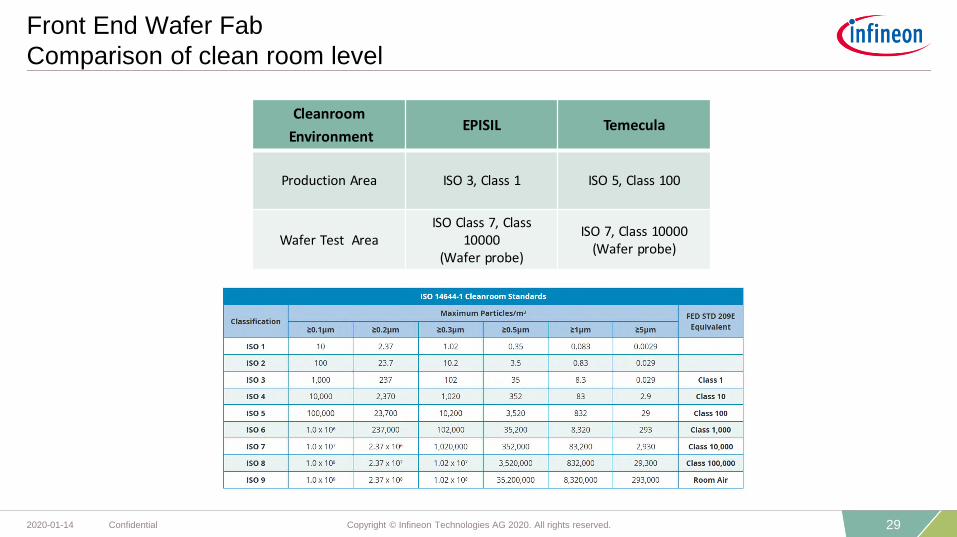
Front End Wafer Fab Comparison of clean room level
Cleanroom
EnvironmentEPISIL Temecula
Production Area ISO 3, Class 1 ISO 5, Class 100
Wafer Test AreaISO Class 7, Class
10000(Wafer probe)
ISO 7, Class 10000(Wafer probe)
292020-01-14 Confidential Copyright © Infineon Technologies AG 2020. All rights reserved.

Copyright © Infineon Technologies AG 2020. All rights reserved. 30
Agenda
Motivation of the change
PCN details
5M+1E Difference
5M+1E Difference Front End
Comparison of clean room level Front End (Environment)
Operator training system Front End (Man)
Equipment comparison Front End (Machine)
Structure comparison table & Materials Front End (Material)
1
2
3
4
5
6
7
8
2020-01-14 Confidential

Front End Wafer Fab EPISIL Training & Development Cycle
New Employee Orientation(HR)
Orientation(MFG)
Basic Training &Basic Subjects Evaluation
Skill Training(Machine Operation)
Certification &Evaluation
Re-training
Re-certification &Re-evaluation
Employ/ Allow to operate certified machines
Dismiss/Forbid to operate the uncertified machines
Qualified
Qualified
Disqualified
Disqualified
Learning new machine&Regular Certification
312020-01-14 Confidential Copyright © Infineon Technologies AG 2020. All rights reserved.

Front End Wafer Fab EPISIL Certification Process
The Operator Completed Study and Can Operate
Independently
Subject Certification Application
Conduct Online Certification in the System
Technical Certification Application
Check Subject Certification Result
Re-training
Re-training
Certification & Evaluation
by the Engineer
Fail
Fail
Pass
Pass
Log the Certification Score to the System/
Allow to operate certified machines
322020-01-14 Confidential Copyright © Infineon Technologies AG 2020. All rights reserved.

Front End Wafer Fab Temecula Training & Certification System
› Operator training and certification requires
– Orientation and Basic Training– Need to Pass Test
– Specialized Training for every Process / Tool– Complete required minimum hours of on the job training– Pass certification test
– Certification will be documented in the training system– MES system will be updated to allow the operator track in/track out for the certified
process– Certification expires after one year
– Recertification required within one month,– Otherwise MES system update to disable operator
Sifo and TEM training systems are similar
332020-01-14 Confidential Copyright © Infineon Technologies AG 2020. All rights reserved.

Front End Wafer Fab Temecula Training & Certification
New Employee Orientation
(Safety, HR, Mfg, Quality)
Basic Training
Skill Training(Machine/Process Operation)
Certification &Evaluation
Re-training
Re-certification &Re-evaluation
Update MES System to allow the operator theoperation of certified machines/processes
Qualified
Qualified
Disqualified
Certification &Evaluation
Re-training
Disqualified
342020-01-14 Confidential Copyright © Infineon Technologies AG 2020. All rights reserved.

Copyright © Infineon Technologies AG 2020. All rights reserved. 35
Agenda
Motivation of the change
PCN details
5M+1E Difference
5M+1E Difference Front End
Comparison of clean room level Front End (Environment)
Operator training system Front End (Man)
Equipment comparison Front End (Machine)
Structure comparison table & Materials Front End (Material)
1
2
3
4
5
6
7
8
2020-01-14 Confidential

Front End Wafer Fab Gen5 ATV MOS Equipment Comparison
› Future Changes will be accessed accordingly to Infineon Change Management Business Process
› Substrate and chemicals share the same specification.
› Total number for Gen5 ATV MOS flow is 150 steps. 90% step are running in different tools.
› All unit processes are matched to the reference site to have comparable process performance
No Breakdown of Tool Delta Assessment
1 CVD (LPCVD/APCVD)Comparable Process
Performance
2 Etch (dry & wet)Comparable Process
Performance
3 Furnace (anneal)Comparable Process
Performance
4 ImplantComparable Process
Performance
5 LithoComparable Process
Performance
6 Wet (clean)Comparable Process
Performance
7Thin film (PVD: top metal & back
metal)Comparable Process
Performance
8 GrindingComparable Process
Performance
362020-01-14 Confidential Copyright © Infineon Technologies AG 2020. All rights reserved.

General Process Controls of Gen5 ATV MOS(Process Equipment controls / inline/offline key item monitoring)
› After FOX/Gate OX/ Poly gate deposition- thickness measurements
› After litho- optical inspection- critical dimension measurement (CD measurements)- alignment spec measurement
› After Implant- Rs monitoring on control wafer
› After etching- critical dimension measurement (CD measurements)
› Metal deposition- Rs monitoring on control wafer for each layer
› Defect density controls - monitoring (two wafers / Lot) - screening (100% inking)
› Wafertest- Cp/Cpk monitoring- screening (100% inking)
372020-01-14 Confidential Copyright © Infineon Technologies AG 2020. All rights reserved.

Copyright © Infineon Technologies AG 2020. All rights reserved. 38
Agenda
Motivation of the change
PCN details
5M+1E Difference
5M+1E Difference Front End
Comparison of clean room level Front End (Environment)
Operator training system Front End (Man)
Equipment comparison Front End (Machine)
Structure comparison table & Materials Front End (Material)
1
2
3
4
5
6
7
8
2020-01-14 Confidential

Front End Materials
Items Temecula Episil
WaferSupplier SMaterial: Silicon/EPI
Supplier SMaterial: Silicon/EPI
GasSupplier AMaterial: A
Supplier A’Material: A
Wet ChemicalSupplier BMaterial: B
Supplier B’Material: B
FilmSupplier CMaterial: C
Supplier C’Material: C
ImplantSupplier DMaterial: D
Supplier D’Material: D
Photo ChemicalSupplier EMaterial: Photo resist
Supplier E’Material: Photo resist
Top MetalSupplier FMaterial: Al/Si
Supplier F’Material: Al/Si/Cu
Back metalSupplier GMaterial: Cr/Ni/Ag
Supplier G’Material: Ti/Ni/Ag
› Key materials are the same between two sites
› (Note: Supplier A’ represents different supplier from Supplier A and similarly B’ from B etc….)
392020-01-14 Confidential Copyright © Infineon Technologies AG 2020. All rights reserved.

Copyright © Infineon Technologies AG 2020. All rights reserved. 40
Agenda
Process flow comparison & Wafer shipping box Front End (Method)
Advanced Measurement System Analysis Front End (Measurement)
5M+1E Difference Back End
Comparison of clean room level Back End (Environment)
Operator training system Back End (Man)
Equipment comparison Back End (Machine)
Structure comparison table & Materials Back End (Material)
Process flow comparison & Wafer shipping box Back End (Method)
9
10
11
12
13
14
15
16
2020-01-14 Confidential

Front End Wafer FabGen5 ATV MOS Process Flow
Poly GateChannel
WellSource Well
Contact Implant
ILD Contact Top metal
BACKEND
Assembly
BACKEND
Assembly
Temecula
Wafer Test
Temecula
Wafer Test
Temecula
Backside
Temecula
Backside
Episil
Backside
Episil
Backside
Temecula
Wafer Fab
Temecula
Wafer Fab
Episil
Wafer Fab
Episil
Wafer Fab
Episil
Wafer test
Episil
Wafer test
Infineon
Die banks
Infineon
Die banks
Infineon
Die banks
Infineon
Die banks
Passivation
Thinning Back Metal.
Probing AVI. MDE.
Package Final test.
Epi FOX
412020-01-14 Confidential Copyright © Infineon Technologies AG 2020. All rights reserved.

Comparison Table
Front End Wafer Fab Comparison
Temecula EPISILImprovements/
Remarks
Top Metal Material Al/1%Si Al/1%Si 0.5%CuIndustry commonly used composition (good in Electro-Migration performance)
Top Metal Thickness 4.5 um 5.5 umThicker metallization to eliminate ILD cratering risk in assembly
Backside metal MaterialCr/Ni-VD/Ag Ti/Ni/Ag
EPISIL backside metal scheme in the past 10 years without peeling & Rdson matches well to Temecula
422020-01-14 Confidential Copyright © Infineon Technologies AG 2020. All rights reserved.

Process Capability and Cpk Comparison› Cp and Cpk, commonly referred to as process capability indices, are used to define the ability of a
process to produce a product that meets requirements. These indices greatly simplifies the management of statistically controlled processes.
› This Cpk index is calculated using specification limits, the standard deviation, and the mean. The index indicates whether the process is capable of producing within specification and is also an indicator of the ability of the process to adhere to the target specification.
› In Infineon we use Cpk => 1.66 as a critieria to ensure process is running with high stability on target specifications.
› Inline and electrical probing parameters are synchronized between EPISIL and Temecula.– Comparable cpk results for inline/offline PPAP parameters and additional key inline
parameters.
– Technology dimensions are comparable and proof comparable process performance independentof equipment differences.
– Comparable cpk results for electrical parameters.– Electric performance is comparable and proofs comparable electric behavior independent of
equipment differences.
432020-01-14 Confidential Copyright © Infineon Technologies AG 2020. All rights reserved.

Production Process StabilityTemecula vs. Episil
1) Critical Global SPC items in process FMEA>1.67Temecula Episil Corrective Action (Cpk <1.67) Comment
Area Description Cpk Cpk
Diffusion Field oxidation thickness NA 2.68
Diffusion Gate oxidation thickness 3.47 1.97
Diffusion Poly Deposition thickness 3.64 2.37
Diffusion Poly Deposition Rs NA 2.37
CVD Interlayer Dielectric thickness 2.26 1.86
CVD Interlayer Dielectric Phos content NA 1.82
CVD Passivation film thickness NA 1.75
CVD Passivaton Phos Content 4.90 1.90
Dry Etch Contact OX etch rate 2.40 3.44
Dry Etch Contact Si etch rate 2.56 1.96
Implant As implant Rs 2.56 2.44
Implant P implant Rs 1.88 2.35
Implant B implant Rs 2.00 2.20
Thin films Cr or Ti deposition 2.36 2.13
Thin films Ni deposition 4.22 1.93
Thin films Ag deposition 2.00 2.03
Thin films Al deposition 2.32 2.00
Photo Gate poly alignment X 1.84 2.69 EPISIL uses tightening spec (+/- 0.25 um) vs Temecula (+/-0.4 um)
Photo Gate poly alignment Y 1.84 2.69EPISIL uses tightening spec (+/- 0.25 um) vs Temecula (+/-0.4 um)
Photo Contact alignment X 2.18 2.30EPISIL uses tightening spec (+/- 0.25 um) vs Temecula (+/-0.4 um)
Photo Contact alignment Y 2.53 2.30EPISIL uses tightening spec (+/- 0.25 um) vs Temecula (+/-0.4 um)
Photo Gate poly CD NA 2.16
Photo Contact CD NA 2.66
Etch Gate poly CD NA 4.19
Etch Contact CD NA 1.84
Wet etch Metal etch rate NA 1.83
Wet etch Oxide etch rate 3.47 2.16
Wet etch Backside Si Etch rate 1.81 2.00
442020-01-14 Confidential Copyright © Infineon Technologies AG 2020. All rights reserved.

Copyright © Infineon Technologies AG 2020. All rights reserved. 45
Agenda
Process flow comparison & Wafer shipping box Front End (Method)
Advanced Measurement System Analysis Front End (Measurement)
5M+1E Difference Back End
Comparison of clean room level Back End (Environment)
Operator training system Back End (Man)
Equipment comparison Back End (Machine)
Structure comparison table & Materials Back End (Material)
Process flow comparison & Wafer shipping box Back End (Method)
9
10
11
12
13
14
15
16
2020-01-14 Confidential

General information on AMSA / Gauge R&R analysis procedure
› The Advanced Measurement System Analysis (AMSA) methodology, which is based on the “Gauge R&R” procedure, is a fast and efficient tool to:
– analyze and assess the test performance
– identify test instabilities (Repeatability, Reproducibility, Bin flipping)
– evaluate the impact of the measurement process on the overall yield
› Gauge R&R method:
– The GR&R method is a widely used and recognized procedure to assess the statistical properties of reproducibility and repeatability of measurement systems. Based on this statistical procedure a GR&R value can be calculated giving an indicationon the variability of the test system. At Infineon, the variability is classified as excessive if GR&R >25%. Hence, tests with GR&R > 25% are reported in this document. In addition, tests with GR&R > 10% are evaluated Infineon internally.
– Hereby, reproducibility and repeatability are defined as:
– Reproducibility: is the variation of several measurements obtained by using different measuring equipment for measuring the identical characteristic on the same part.
– Repeatability: is the variation of several measurements obtained by using the same measuring equipment for measuring the identical characteristic on the same part.
462020-01-14 Confidential Copyright © Infineon Technologies AG 2020. All rights reserved.

Gr&R Results
› All critical parameters PASS (less than 25%)– Threshold voltage@5V (VP@5V)– BVDSS @ 250 uA (BVDSSA250)– Diode forward voltage, Vf@5A (VF@5A)– Source-Drain Leakage@55V (IDSS@55V)– Gate-Source Leakage@20V (IGSS@20V)
472020-01-14 Confidential Copyright © Infineon Technologies AG 2020. All rights reserved.

Copyright © Infineon Technologies AG 2020. All rights reserved. 48
Agenda
Process flow comparison & Wafer shipping box Front End (Method)
Advanced Measurement System Analysis Front End (Measurement)
5M+1E Difference Back End
Comparison of clean room level Back End (Environment)
Operator training system Back End (Man)
Equipment comparison Back End (Machine)
Structure comparison table & Materials Back End (Material)
Process flow comparison & Wafer shipping box Back End (Method)
9
10
11
12
13
14
15
16
2020-01-14 Confidential

5M+1E DifferencesBack End Assembly Site Extension (DSO8)
ATM is added as an Assembly Site
No ItemsComparison
Concerning point Check Items Check result EvidenceExisting After PCN
1 Environment BE Carsem, Malaysia BE ATM, MalaysiaLower yield due to higher particle level
Clean room cleanliness spec Defect density on wafers
ATM has comparable clean room defect performance.
Clean room cleanliness spec
2 Man BE Carsem, Malaysia BE ATM, MalaysiaMiss-operation due to lack of operator training and certification
Operator training and certification system
The same level of training and certification system is implemented in ATM
Operator training and certification systempresentation
3 MachineBE Carsem, Malaysia Equipment
BE ATM, Malaysia EquipmentProduct performance and reliability risk
In-line / off-line process parameterElectrical distributionQualification results
In-line/ off-line process parameter, And Electrical distribution are comparablebetween the sites
Electrical distributionQualification resultsMachine comparison tableCpk Performance
4 MaterialBE Carsem, Malaysia Material
BE ATM, Malaysia MaterialProduct performance and reliability risk
In-line / off-line process parameterElectrical distributionQualification results
In-line/ off-line process parameter, And Electrical distribution are comparablebetween the sites
Electrical distributionQualification resultsMaterial comparison table
5 MethodOperator sets strips magazine to machine in all process
Operator sets strips magazine to machine in all process
Product performance and reliability risk and wafer damage during the transfer
In-line / off-line process parameterElectrical distributionQualification resultsWafer shipping
In-line/ off-line process parameter, And Electrical distribution are comparablebetween the sites
Electrical distributionQualification resultsCpk PerformancePictures of wafer shipping box
6 MeasurementTest site Carsem, Malaysia
Test site ATM, Malaysia Data matchingFinal test comparisonElectrical distribution
Comparable performance Final test comparisonElectrical distributionQualification results
492020-01-14 Confidential Copyright © Infineon Technologies AG 2020. All rights reserved.

Copyright © Infineon Technologies AG 2020. All rights reserved. 50
Agenda
Process flow comparison & Wafer shipping box Front End (Method)
Advanced Measurement System Analysis Front End (Measurement)
5M+1E Difference Back End
Comparison of clean room level Back End (Environment)
Operator training system Back End (Man)
Equipment comparison Back End (Machine)
Structure comparison table & Materials Back End (Material)
Process flow comparison & Wafer shipping box Back End (Method)
9
10
11
12
13
14
15
16
2020-01-14 Confidential

Back End Assembly Site Extension (DSO8) Comparison of clean room level
Cleanroom
EnvironmentCarsem ATM
Die bank/Front of line
(Wafer mount to Internal QC)ISO 7, Class 10000 ISO 7, Class 10000
End of line
(Molding to Final Inspection)ISO 8, Class 100000 ISO 8, Class 100000
Final Test ISO 8, Class 100000 ISO 8, Class 100000
512020-01-14 Confidential Copyright © Infineon Technologies AG 2020. All rights reserved.

Copyright © Infineon Technologies AG 2020. All rights reserved. 52
Agenda
Process flow comparison & Wafer shipping box Front End (Method)
Advanced Measurement System Analysis Front End (Measurement)
5M+1E Difference Back End
Comparison of clean room level Back End (Environment)
Operator training system Back End (Man)
Equipment comparison Back End (Machine)
Structure comparison table & Materials Back End (Material)
Process flow comparison & Wafer shipping box Back End (Method)
9
10
11
12
13
14
15
16
2020-01-14 Confidential

Back End Assembly SiteCarsem Training
Copyright © Infineon Technologies AG 2020. All rights reserved.
Theory class training Snap test
OJT
Training
Machine Operating Qualification
Pass?Yes
No
Theory certification test
Pass?Yes
NoMES access right
granted
Notify supervisor
Fail Practical
Failed 2x
Upon completion mandatory training
Fail 1st & 2nd attempt
Fail 3rd attempt
Practical
Theory
Release torun production
Updateskill matrix
Failed 2x
532020-01-14 Confidential Copyright © Infineon Technologies AG 2020. All rights reserved.

Back End Assembly SiteATM Training
Recertification InductionTraining
ProcessTraining
OJT Certification
& CIM registration
Assign to work
New IntakeOperator
Existing Operator :› Transfers to a New Process› Additional Skill (Multi-skill) › Cross Train At Different Product / Process› Long Absent ( >30 Days )› De-Certification / Disqualification :
- Release Operatorto Actual Processto Conduct Routine Task.
- CIM will ONLY allow certified person to operate certified process/machine.
- Perform Minimum 3 Lot Acceptance Qualification (LAQ).
Focus On Process Station Knowledge-Standard Working Method-Direct / Indirect Material
Control Method-Product Handling Method-Defect Management(Criteria, Inspection &
Identification Method)Management-Abnormal Control Method-Recording Method-Basic SPC-**Automotive Product Control Education (Applicable for Automotive
Line)
Assign Operator toActual Process for Hands-On /Skill Up/Observation
-Learn and Work together withexperienced operator
-Perform Min 3 lots Acceptance Qualification (LAQ)
-Perform Trap simulation to Confirm Effectiveness
-Certify OperatorCompetency By
Updating Operator OJT Record
- Judged and approved by Trainer, Supervisor and Manager
- Register Operator ID into CIM system based on her certified process/machine.
Perform RegularRe-Certification Program Half Yearly
* Focus on Process Standard Work Method* Product & Process Specification- Automotive (MP Cotrol)- Quality Mindset Awareness- Past CAR/MRB Lesson Learn)- SPC
- Basic MFG Process- Basic Quality Control- Operation Recording- Yield & Net Calculation- Theory Assessment- Process Control Tools- Total Control Methodology - Out Of Control Action Plan (OCAP)
Perform RegularRe-Certification Program Yearly
* Focus on Process Standard Work Method* Product & Process Specification- Quality Mindset Awareness- Past CAR/MRBLesson Learn- SPC
Onboarding Orientation (HR/FD/HC)- Registration- Safety Briefing- ATM Overview- Terms & Condition- Responsible Business Alliance (RBA) Policy- Standard of Conduct- Security Briefing- Basic Education For New Employees- QualityFIRST Mindset
542020-01-14 Confidential Copyright © Infineon Technologies AG 2020. All rights reserved.

Copyright © Infineon Technologies AG 2020. All rights reserved. 55
Agenda
Process flow comparison & Wafer shipping box Front End (Method)
Advanced Measurement System Analysis Front End (Measurement)
5M+1E Difference Back End
Comparison of clean room level Back End (Environment)
Operator training system Back End (Man)
Equipment comparison Back End (Machine)
Structure comparison table & Materials Back End (Material)
Process flow comparison & Wafer shipping box Back End (Method)
9
10
11
12
13
14
15
16
2020-01-14 Confidential

Back End Assembly Site Gen5 ATV MOS Equipment Comparison
› All processes are matched to the reference site to have comparable process performance
No Breakdown of Tool Delta Assessment Remarks
1 Wafer mount Comparable Process Performance
2 Wafer sawing Comparable Process Performance
3 Die attach Comparable Process Performance
4 Plasma Comparable Process Performance
5 Wire Bond Comparable Process Performance
6 Primer Comparable Process Performance
7 Molding Comparable Process Performance
8 Deflash Comparable Process Performance
9 Plating Comparable Process Performance
10 Trim&Form Comparable Process Performance
11 Test Comparable Process Performance
562020-01-14 Confidential Copyright © Infineon Technologies AG 2020. All rights reserved.

Copyright © Infineon Technologies AG 2020. All rights reserved. 57
Agenda
Process flow comparison & Wafer shipping box Front End (Method)
Advanced Measurement System Analysis Front End (Measurement)
5M+1E Difference Back End
Comparison of clean room level Back End (Environment)
Operator training system Back End (Man)
Equipment comparison Back End (Machine)
Structure comparison table & Materials Back End (Material)
Process flow comparison & Wafer shipping box Back End (Method)
9
10
11
12
13
14
15
16
2020-01-14 Confidential

Back End Materials comparison for ATV DSO8 MOSFET
Items Carsem ATM
LeadframeSupplier AMaterial: A
Supplier A’Material: A
Solder wireSupplier BMaterial: B
Supplier BMaterial: B
Bonding wireSupplier CMaterial: C
Supplier CMaterial: C
Adhesion Promoter(Primer)
Supplier DMaterial: D
Supplier DMaterial: D
Mold compoundSupplier EMaterial: E
Supplier EMaterial: E
Plating Material: F Material: F
› Key materials are the same between two sites
› (Note: Supplier A’ represents different supplier from Supplier A and similarly B’ from B etc….)
582020-01-14 Confidential Copyright © Infineon Technologies AG 2020. All rights reserved.

Copyright © Infineon Technologies AG 2020. All rights reserved. 59
Agenda
Process flow comparison & Wafer shipping box Front End (Method)
Advanced Measurement System Analysis Front End (Measurement)
5M+1E Difference Back End
Comparison of clean room level Back End (Environment)
Operator training system Back End (Man)
Equipment comparison Back End (Machine)
Structure comparison table & Materials Back End (Material)
Process flow comparison & Wafer shipping box Back End (Method)
9
10
11
12
13
14
15
16
2020-01-14 Confidential

Back End Assembly Site Process Flow for ATV DSO8
› Test
Shipping
To customer
Shipping
To customer
Carsem
Final Test
Carsem
Final Test
Carsem
Assembly
Carsem
Assembly
ATM
Assembly
ATM
Assembly
Carsem
Pre-Assembly
Carsem
Pre-Assembly
ATM
Pre-Assembly
ATM
Pre-Assembly
ATM
Final Test
ATM
Final Test
Carsem
Packing
Carsem
Packing
ATM
Packing
ATM
Packing
Die Attach Wire Bond
Final Test Inspection
Wafer Mounting
Wafer Sawing
Inspection
Molding PMC Deflash Plating Trim Form
Packing QA Final
Laser Marking
Visual Inspecion
Inspection
DA CurePlasma clean
602020-01-14 Confidential Copyright © Infineon Technologies AG 2020. All rights reserved.

Part Marking Comparison
› Example of part marking
Carsem Amkor
612020-01-14 Confidential Copyright © Infineon Technologies AG 2020. All rights reserved.

Copyright © Infineon Technologies AG 2020. All rights reserved. 62
Agenda
Final Test Comparison Parameter Results (Measurement)
Electrical Distribution Results
Qualification test report
17
18
19
2020-01-14 Confidential

Back End Assembly Site ExtensionFinal Test Comparison
Vth_250uA Rdson_10V_3.4A
632020-01-14 Confidential Copyright © Infineon Technologies AG 2020. All rights reserved.

Back End Assembly Site ExtensionFinal Test Comparison
Bvdss_250uA Vsd_2A
642020-01-14 Confidential Copyright © Infineon Technologies AG 2020. All rights reserved.

Back End Assembly Site ExtensionFinal Test Comparison
Igss_+20V Igss_-20V
652020-01-14 Confidential Copyright © Infineon Technologies AG 2020. All rights reserved.

Back End Assembly Site ExtensionFinal Test Comparison
Idss_55V
662020-01-14 Confidential Copyright © Infineon Technologies AG 2020. All rights reserved.

Copyright © Infineon Technologies AG 2020. All rights reserved. 67
Agenda
Final Test Comparison Parameter Results (Measurement)
Electrical Distribution Results
Qualification test report
17
18
19
2020-01-14 Confidential

Electrical parameters 25oC/Ambient – DSO8
Note: Control is Temecula Fab and Qual is EPISIL Fab
682020-01-14 Confidential Copyright © Infineon Technologies AG 2020. All rights reserved.

Electrical parameters 25oC/Ambient – DSO8
Note: Control is Temecula Fab and Qual is EPISIL Fab
692020-01-14 Confidential Copyright © Infineon Technologies AG 2020. All rights reserved.

Electrical parameters -40oC/Cold – DSO8
Note: Control is Temecula Fab and Qual is EPISIL Fab
702020-01-14 Confidential Copyright © Infineon Technologies AG 2020. All rights reserved.

Electrical parameters -40oC/Cold – DSO8
Note: Control is Temecula Fab and Qual is EPISIL Fab
712020-01-14 Confidential Copyright © Infineon Technologies AG 2020. All rights reserved.

Electrical parameters 175oC/Hot – DSO8
Note: Control is Temecula Fab and Qual is EPISIL Fab
722020-01-14 Confidential Copyright © Infineon Technologies AG 2020. All rights reserved.

Electrical parameters 175oC/Hot – DSO8
Note: Control is Temecula Fab and Qual is EPISIL Fab
732020-01-14 Confidential Copyright © Infineon Technologies AG 2020. All rights reserved.

Copyright © Infineon Technologies AG 2020. All rights reserved. 74
Agenda
Final Test Comparison Parameter Results (Measurement)
Electrical Distribution Results
Qualification test report
17
18
19
2020-01-14 Confidential

Qualification Summary - Carsem
Note: Qual Test Vehicles are products put into Reliability Stress Test and represents the matrix parts which are then qualified by similarity.
752020-01-14 Confidential Copyright © Infineon Technologies AG 2020. All rights reserved.
Qual Test Vehicle /
Qual by Matrix
AUIRF7342QTR DSO8 G5 1.2 55 450 22687 Qual Test Vehicle CSM
AUIRF7309QTR DSO8 G5 0.8 30 450 22687 Matrix CSM
AUIRF7379QTR DSO8 G5 0.8 30 450 22687 Matrix CSM
AUIRF7316QTR DSO8 G5 1.2 30 450 22687 Matrix CSM
AUXHMF7321D2 DSO8 G5 1.2 30 450 22687 Matrix CSM
AUIRF7343QTR DSO8 G5 1.2 55 450 22687 Matrix CSM
94-3447PBF DSO8 G5 1.2 55 450 22687 Matrix CSM
Part Number Package Gen Die Size Voltage Gox QRP# Site

Qualification Summary - Amkor
Note: Qual Test Vehicles are products put into Reliability Stress Test and represents the matrix parts which are then qualified by similarity.
762020-01-14 Confidential Copyright © Infineon Technologies AG 2020. All rights reserved.
Qual Test Vehicle /
Qual by Matrix
AUIRF7343QTR DSO8 G5 1.2 55 450 22908 Qual Test Vehicle ATM
AUIRF7309QTR DSO8 G5 0.8 30 450 22908 Matrix ATM
AUIRF7316QTR DSO8 G5 1.2 30 450 22908 Matrix ATM
AUXHMF7321D2 DSO8 G5 1.2 30 450 22908 Matrix ATM
94-3447PBF DSO8 G5 1.2 55 450 22908 Matrix ATM
AUIRF7342QTR DSO8 G5 1.2 55 450 22908 Matrix ATM
Voltage Gox QRP# SitePart Number Package Gen Die Size

Qualification Summary – CarsemRel#22687
772020-01-14 Confidential Copyright © Infineon Technologies AG 2020. All rights reserved.

Qualification Summary – AmkorRel#22908
782020-01-14 Confidential Copyright © Infineon Technologies AG 2020. All rights reserved.

2020-01-14 Confidential Copyright © Infineon Technologies AG 2020. All rights reserved. 79

Sales name SP number OPN Package
94-3447PBF SP001517084 94-3447PBF PG-DSO-8-902
AUIRF7309QTR SP001521596 AUIRF7309QTR PG-DSO-8-902
AUIRF7316QTR SP001518472 AUIRF7316QTR PG-DSO-8-902
AUIRF7342QTR SP001517224 AUIRF7342QTR PG-DSO-8-902
AUIRF7343QTR SP001517450 AUIRF7343QTR PG-DSO-8-902
AUIRF7379QTR SP001520160 AUIRF7379QTR PG-DSO-8-902
AUXHMF7321D2 SP001522944 AUXHMF7321D2 PG-DSO-8-902
Final PCN: Several changes affecting Gen 5P Mosfets for DSO8 packagePCN N° 2019-184-A2
1_cip19184_A2 Page 1 of 1 3/8/2021