Pradeep_Naveen_Navin.pdf - RRI Digital Repository
88
PROJECT REPORT ON TWO AXES, MICRO POSITIONfPvG CON'IT170%LEK CARRIED OUT AT RADIO ASTRONOMY LAB I~AMAN IZI~SIM~~CII rivsrrrrrurr7u IlANGAIJOIi12 UNDER THE ESTEEMED GUI IIANCI~~ Or; Mr-. ANANrl'IIAS IJI~IiAMhN IAN ENGINEER, R.R.I. SUBMITTED TO BANGALORE UNIVERSITY IN PARTIAL FULFILLMENT FOR THE AWARD OF DEG,REE OF wtcrmrJoIi ov ICNGIN~CEJ~ING IN ICIdECI'IIONICS AN I) COMMUNICAl'lO!.I. LECTURER INCHARGE Mr. I<.V.MI JIL41JII)~I.~41~ 1B.I.T. BANGALORE DEPARTMENT OF ELECTRONICS APiD COMMUNICATION BANGALORE INSTITUTE OF 'rECHNOLOGY K.R.ROAD, BANGALORE-56OIM4 BANGALORE UNIVERSITY
-
Upload
khangminh22 -
Category
Documents
-
view
4 -
download
0
Transcript of Pradeep_Naveen_Navin.pdf - RRI Digital Repository

PROJECT REPORT ON
TWO AXES, MICRO POSITIONfPvG CON'IT170%LEK
CARRIED OUT AT
RADIO ASTRONOMY LAB I ~ A M A N I Z I ~ S I M ~ ~ C I I rivsrrrrrurr7u
IlANGAIJOIi12
UNDER THE ESTEEMED GUI I I A N C I ~ ~ Or; Mr-. ANANrl'IIAS IJI~IiAMhN IAN
ENGINEER, R.R.I .
SUBMITTED TO BANGALORE UNIVERSITY I N PARTIAL FULFILLMENT FOR THE AWARD OF DEG,REE OF
w t c r m r J o I i ov I C N G I N ~ C E J ~ I N G IN ICIdECI'IIONICS AN I ) COMMUNICAl'lO!.I.
LECTURER INCHARGE Mr. I<.V.MI JIL41JII)~I.~41~
1B.I.T. BANGALORE
DEPARTMENT OF ELECTRONICS APiD COMMUNICATION BANGALORE INSTITUTE OF 'rECHNOLOGY
K.R.ROAD, BANGALORE-56OIM4 BANGALORE UNIVERSITY

DEPARTMENT OF ELECTRONICS AND COMMUNICATION
BANGALORE INSTITUTE OF TECHNOLOGY
7 k a ie l ~ , cent& c%z$ &e ++ww t&
Two Axes Micro-positioning Controller hk-&lfed+A--46waew
Pradeep S. M.R.Naveen Navin Rajendran P.C. i . p m & d & p h ? d a & ~ @ & d c v a n d o & ~ ' O & F ~
~ & £ ~ ~ r w d ~ ~ & t ~ ~ ~
A & 1496- 97,
7 & @ * c l r d ~ e c w r i e d & a t
Raman Research Institute,Bangalox-e.
P* 6% &L,&W ~r.~ .~ .~nanthasubramani 'an,
Lecturer, ( 4 ( ~ ( 9 ~ Engineer, Dept. of E & C . R.R.I.
B .I.T.
Prof.M.J.ShantiPrasad, H.O.D., E & C,
B .IT.

RAMAN RESEARCH INSTITUTE C.V.Raman Avenue, Sadashivanagar, Bangalore - 560 080 India
This is to certify that the project work entitled "Two axes Micro-
positioning Controller" was carried out by Pradeep S., M.R.Naveen and
Navin Rajendran P.C. in the Radio Astronomy Laboratory of the Raman
Research Instt'hte, Bangalore under my guidance for the partial ful&ent
of the requirements for the award of Bachelor of Engirheering degree in
Electronics and Communication of the Bangalore University, Bangalore.
P a & -
( P.G. ANANTBASUBRAMANIAN ) ENGINEER.
Phone : +9 1 (80) 334 0 1 22 Fox : 334 0492 e-mail : r o a t 8 r r i e r n e t i n


ACKNOWLEDGEMENTS
Firstly , we wish to express our sincere thanks to Prof. NARAYANAPPA, former
Head of department of Electronics , B.I.T. , Bangalore , for guiding us to this institute for a
project.
We thank the Director of Raman Research Institute Prof. N.KUMAR and
Dr.D.K.RAVINDRA, Head, Radio Astronomy Lab in R.R.I. for providing us the facilities to
carry out this project work successfully.
We thank our guide Mr. P.G.ANANTH[ASUBRAMANIAN, Engineer, at RRI, for
motivating and leading us successfully through the twists and turns of the project.
We also thank Prof . SHANTI PRASAD, the H.O.D., for his guidance during the
course of the project. Mr. K.V. MURALIDHAR, lecturer , B.I.T. is worthy of our
deepest gratitude for his kind help throughout the course of the project work.
A project of this nature could not have been possible without the help of many people
in R.R.I.
Mr. H. Nagaraj, for careful design of the PCB layout and helping in getting the
fabricated board in time for assembly and testing.
Mr.Girish and Mrs.Seetha at the M.M.W. lab
Mr.Muthu and Mr.Snresh at theWork5hap
Mr.Raju Varghese, the photogl-apher
Mr. K. Ramesh and McGu~wki~xn for helping us with the installation of the
EPROM programmer and guiding us in certain aspects of serial communication.
Finally, we thank Mr. K.B.Ragl1avendra Rao for helping us in the laboratory and
also in getting this report done.
Our stay at the R.R.I. was a very enlightening one. We gained insight into the practical
aspects of designing electronic circuits of a varied nature, and learnt a lot from the mistakes we
had commited inadvertently. We spent so much time at the R.R.I. that it almost became our
second home.
PRADEEP S. NAVEEN M.R. NAVIN RAJENDRAN P.C.

CONTENTS
1. Introduction
1.1 Existing system 1.2 Requirements 1.3 Description
2. Hardware
Microcontroller Memory Digital to Analog Converter Pullse Width Modulator Driver Analog Multiplexer Power Supply Requirements Reference Design Interrupt Control Serial Communication Hardware Corrections
3. Software
3.1 Program Description 3.2 Flowcharts
4. Conclusion
5. Appendix
Photographs Schematics
PCB layout Listing of Components
i iii
Data Sheets Bibliography


INTRODUCTION
1.1 Existing system :
The mm. wave receiver used with the 10.4m mm-wave Telescope in the
R.R.I. uses a mechanically tunable Wide-Band Gunn Oscillator for the 1 st down
conversion of the R.F. signals in the frequency range 80 - 115 GHz.
The present system of setting the olp frequency and power of the Gunn
oscillator involves manual adjustment of the two micro-meters as per special charts
that give the required readings of the p-meters for specific values of frequency and the
corresponding values for peak power. A person who wishes to set a particular
frequency of the Gunn oscillator has to manually turn the tuning the respective p-meter
to the values in the chart.
1.2 Requirements:
In general, each frequency setting on the Gunn oscillator has a corresponding
position for peak power olp . Eight such L.O.frequencies are commonly employed for
the mrn. wave observations using the radio telescope.
A control panel has to be provided such that an operator can
+ choose any of the 8 frequency and corresponding power settings.
+ startlstop the p-meters as and when required.
+ select any of the p-meters, change its direction and move it in discrete steps for
minor adjustments.
When changing from one frequency setting to another in the pre-decided eight
settings, the y-meters should automatically be set to the desired value of the frequency
& power.
Dept. of Electronics and Communication, B.I.T. ,1996-97

Introduction
A facility should be provided such that a P.C. can control the frequency &
power settings from a remote location.
The power supply will be external to the modules made. The modules will be
provided with the required on-board regulators.
The design aim is to build a prototype module with minimum hardware and a
micro-controller as the heart of the system.
1.3 Brief Description o f the project:
A brief description of the project is provided with the help of four simple block
diagrams.
The micro-controller 8031 is the main control unit in this closed loop system
which controls the position of the motors. The p-meters of the Gunn oscillator are
coupled to the shaft of stepper motors which move in a direction determined by the
micro-controller. Feedback potentiometers are also coupled to the shaft of the motor.
The basic set up of the project is as shown in Block Diagram 1. For a position of the
p-meter there exists a unique voltage on the feedback potentiometer. Therefore there
will be eight different voltages corresponding to eight commonly used frequencies.
These voltages are set on the reference potentiometers which when compared with the
feedback potentiometer determines the direction of rotation required.
For example, from the plot of H206 oscillator, it can be seen that variation of
the p- meter position is monotonous with regard to frequency but not with power.
Hence, it is deduced that reference voltage settings represented by the codes are
monotonic for frequency but not for power. So the codes themselves can determine the
direction for the frequency motor but not for the power motor. The frequency p-
meter(operated between 80 and 1 15GHz) has lesser number of turns than the power
p-meter .
Dept. of Electronics and Communication, B.I.T. , 1996-97

Introduction . __ . _ -- - -- - - -- - -- - ----- _-- _
-
90 95 100 105 110 115 Frequency(G Hz)
Dept. of Electronics and Communication, B.I.T. , 1996-97

The set up consists of two modules. The first module with a front panel has the
facility to set reference voltages for frequency and power. The second has the
following controls on the front panel.
0 A switch labeled LOCAL IREMOTE indicates the mode of operation. When the
switch is in the position LOCAL, settings can be done from the front panel. If
REMOTE mode is selected, all settings are done from a remote location, and the
front panel has no effect on the movement of the p-meters.
Three switches labeled S2, S1 and So are used to set the frequency to one of eight
commonly used values. The required code may be set referring to a chart which
specifies the code for the chosen frequency. The indication of the code is given by
three LEDs placed above the switches.
The START I STOP switch is to start or stop the motor. -
~he-R switch which decides the motor to be used in case of fine movement.
The DIR switch which specifies the direction of rotation, again used only for f i e
movement.
Two independent switches to turn the motors ONIOFF.
The information regarding the switches is read into the controller. The
controller checks the code and decides to perform either fine or coarse movement. In
the case of coarse movement, i.e., when the code has changed, both p-meters are
moved to the desired position. The fine movement is done if the code is the same, and
decisions are made on the basis of the control switches.
. Basically, a stepper motor is operated in full steps by providing digital signals
to the windings, but by providing a sinusoidal signal to one phase and a 90 degree
phase shifted signal to the other phase, micro-stepping is achieved. This increases the
number of steps per revolution i.e., the resolution of the motor. In this application a
200 full step per revolution stepper motor is used in micro-stepping mode to provide a
minimum of 3 600 stepslrevolution.
The sinusoidal signals are stored in look up tables and given sequentially to Digital-
to-Analog Converters (DAC ), the output of which is given to digitally controllable
Dept. of Electronics and Communication, B.I.T. ,1996-97

Introduction
drivers through Pulse Width Modulators. A set of control signals from the controller
also decides the phase and direction of currents.
The two modules as described above are briefly described.
The three block diagrams shows the basic elements of the two modules.
Block diagram 2 shows the various devices connected to the controller. The
memory ( EPROM 27C64 ) is enabled using a decode logic based on the o/p of pins
A13 and PSEN of the controller. The same pins are used to enable a buffer which
reads the control data as shown. The control data includes the following :
+ Information regarding Front panel switches
STA / ST0 ( start /stop the motor )
DIR ( change direction of rotation of the motor ) - L / R ( Local or Remote mode of operation )
+ Status of Limit Switches
L1 (indicates if the freq. pmeter has reached an
extreme)
L2 (indicates if the power pmeter has reached an
extreme)
+ Status of Comparators.
CMPl (status of freq. f h pot compared with chosen
reference)
CMP2 (status of power f h pot compared with chosen
reference)
+LO,Ll and L2 which are the code levels given to MUX to choose one of the eight
reference voltages.
+Tx and Rx for serial transmission and reception through ICL 232.
+DO - D4 are digital signals given to the DAC
+SQ,LA,MO are signals to decide the motor, phase and direction of current.
+ENMI and ENM2 are separate controls to enableldisable the two drivers.
Dept. of Electronics and Communication, B.I.T. ,1996-97
Zntroduction
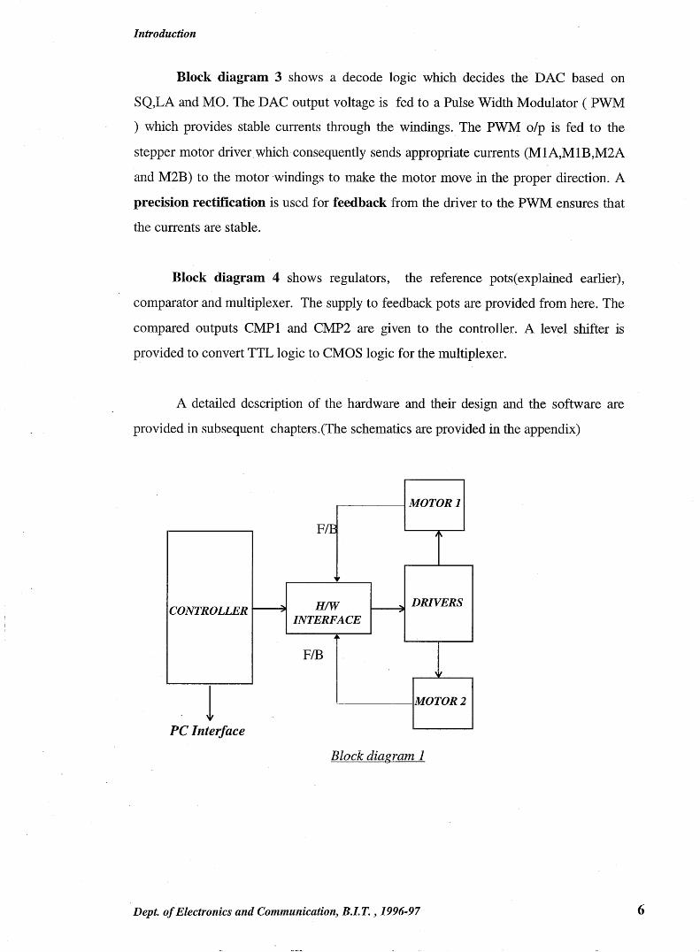
Block diagram 3 shows a decode logic which decides the DAC based on
SQ,LA and MO. The DAC output voltage is fed to a Pulse Width Modulator ( PWM
) which provides stable currents through the windings. The PWM olp is fed to the
stepper motor driver which consequently sends appropriate currents (MlA,MlB,M2A
and M2B) to the motor -windings to make the motor move in the proper direction. A
precision rectification is used for feedback from the driver to the PWM ensures that
the currents are stable.
Block diagram 4 shows regulators, the reference pots(exp1ained earlier),
comparator and multiplexer. The supply to feedback pots are provided from here. The
compared outputs CMPl and CMP2 are given to the controller. A level shifter is
provided to convert TTL logic to CMOS logic for the multiplexer.
A detailed description of the hardware and their design and the software are
provided in subsequent chapters.(The schematics are provided in the appendix)
PC Interface
Block diagram I
Dept. of Electronics and Communication, B.Z.T. ,1996-97

Introduction
-- - Block dz&grarn 2 -- -- --
+12 v
Dept. of Electronics and Communicati~n, B.L T. ,199697
-12 v
v v
- m TX 4 II, 3
ENM2 II,
- DO II,
Dl II,
C
D A T A
0 D2 N + T T 0
D A C
R 0 D3 L , LOGIC
- D LS1 A T A
111, D4 --+
L S ~ II,
CI _I,
C2 111,
LO - L1 - L2 -,
I
----+ +5v C
SUPPLY
MICRO CONTROLLER
80C3 1BH
S E
LA L --b E
C SQ T
_I, I 0 N
MO
1111, L - 0 G
v
4
/ 8 BUFFER

Introduction
PWM D /A
ANDI/V b
A
1 O F 4 4
PRECISION RECTIFIER
A .
v DECODE LOGIC
Block diagram 3
DRIVER
Dept. of Electronics and Communication, B.I. T. ,1996-97 - - -- - - - - - - -

UNREGULATED > = +/-16V < = +/-25v SUPPLY
COMP 1
LEVEL SHIFTER
COMP 2
MUX
REGULATORS +12v -12v
P
Dept. of Electronics and Communication, B.Z.T. ,1996-97 '


Hardware
HARD WARE
2.1 MICROCONTROLLER 80C31BH
The INTEL 8OC31BH is a stand-alone high-performance single-chip computer
fabricated with INTEL'S hghly reliable +5V, depletion mode N-channel silicon gate
HMOs technology and packaged in a 40-pin DIP. It provides the hardware features, .
architectural enhancements and new instructions that make it a powerful and cost-
effective controller for applications requiring upto 64K bytes of program memory and
up to 64K bytes of data storage. The controller also has direct bit-programmable
features.
Features:
128x8RAM
Four 8-bit ports, 32 110 lines
Two 16-bit timerlevent counters
High performance full-duplex serial channel with unique addressing
modes.
External memory expandable to 128K
Five source-two priority level nested interrupt structure
On chip oscillator and clock circuits.
Internal memory address space is further divided into 256 byte internal data RAM and
128 byte Special Function Register(SFR) address spaces, 4 register banks, 128
addressable bits and stack residing in the internal data RAM. AU registers except the
program counter and the four 8-register banks reside in the Special Function Register
space.
Dept. of Electronics and Communication, B.Z.T. ,1996-97
-. * *

Hardware
These memory-mapped registers include the arithmetic register, pointers, IIO
ports, interrupt system register, timers and serial port and special function registers.
128 bit locations in the SFR address space are bit-addressable.
T/O facilities:
Each of the 32 pins are treated as 32 individually addressable bits and also as
four parallel 8-bit ports addressable as ports 0,1,2 and 3.
Port 0 : It is an 8 bit open drain bi-directional IIO port. It is also the multiplexed low
order address and data bus when using external memory.
Port 1 : It is an 8 bit quasi bi-directional YO port. It is used for low -order address
byte during programming and verification.
Port 2 : It is an 8 bit quasi bi-directional I/O port. It also emits the high order 8 bit
address when accessing external memory. It is used for the high order address and
control signals during programming and verification.
Port 3 : It is an 8 bit quasi bi-directional 110 port. It also contains the interrupt, -
timer, serial port and and WR. The secondary functions assigned to the pins of
port 3.
Ports 1 , 2 and 3 can be configured as i/p by writing a 1 into the corresponding
bit latch in the port SFR . The bit latch clocks in a value from the internal bus in
response to a write to latch signal from the CPU.
The level of the port pin itself is placed on the internal bus in response to a
read pin signal.
Ports 1,2,3 when configured as ilp they pull high and will source current when
pulled low.
Degt. of ~lbctronics and Communication, B.I.T. , 1996-97

Hardware
The following table gives the secondary functions of the pins of port 3 and the
assigned configuration as per our application.
CONFIGURATION
Table-1
A 12MHz crystal is connected across XTALl and XTAL2 which are the
input and output of the oscillator high-gain amplifier respectively. The crystal circuit is
given as per the micro-controller specifications. On power-ON, a RESET of lOmsec
is provided.
2.1.a CONTROL WORD:
CONTROL WORD is the data byte which gives certain information to the
controller(shown in the table).This is the main data byte based on which the controller
performs various operations. The CONTROL WORD is accessed as a external
program memory via a buffer(74HCT244) by setting pin A1 3. In order to differentiate
between memory and buffer a decode logic is provided. The instruction to access
external Program memory(M0VC) is used here.
A 1 3 XN Control provided
0 1 Memory is enabled
1 1 Control word buffer is enabled
Dept. of Electronics and Communicatiolz, B.I.T. , 1996-97

Hardware
Control Word Description :
2.1.b FRONT PANEL
The front panel is as shown in the picture(Appendix). It consists of the three
codes So, S1 and S2 which are configured as shown from table 1, and the four bits of
the Control word(START/STOP, FP, DIR and-/R) as shown in table 2. The wiring
of the switches is as shown in the schematic diagram 2 of 5. The code switches are
read only in the LOCAL mode and the controller sets the codes in the REMOTE
mode. The switches are hence enabled only in the LOCAL position of i~ switch.
These switches should not affect the input to the level shifter and should not interfere
with the each other when switched to REMOTE. In order to prevent any such
interference, diodes are used for isolation between themselves , i.e., they are disabled
when t h e r / ~ is in REMOTE position.
Dept. of Electronics and Communication, B.I.T. ,1996-97

Hardware
2.2 MEMORY
EPROM 2 7C64:
27C64 is a single 5V, 64K ultra-violet erasable and electrically
programmable memory[EPROM]. It has an access time of 250ns which is compatible
to high performance microprocessor and micro-controller applications. HMOs -E
technology is used, which is a high speed N-channel MOS Silicon Gate technology.
An important feature is that it has a separate output control and chip enable
CE. The output enable eliminates bus contention in multiple bus micro processor
systems. It has a stand-by mode which reduces power dissipation without increasing
access time. This is done by applying a TTL high signal to the input.
The five modes of operation of the memory are Read, Standby, Program, Program
Verify and Program Inhibit.
Read mode: It has two control functions both of which must be logically satisfied to
obtain data at the outputs. is the power control and should be used for device
selection Data is available at the outputs after the falling edge of m. - C
It is accessed using address pin13(A13) which is connected to OE and PSEN
which enables the chip(=).
The lower address byte is latched by 74HCT573, enabled by ALE from the micro-
controller.
The total memory space utilized by the program is around 2KB. Since it is less
than 4Kbytes, a controller of the same family with in-built memory 87C51 (with a 4K
internal program memory ) may be used. But the advantage here is that the memory .
may be removed when it is required to re-program repeatedly, rather than removing
the controller itself. It also provides an expansion facility.
Dept. of Electronics and Communication, B.Z.T. , 1996-97

Hardware
2.3 DIGITAL TO ANALOG CONVERTER
Digital to Analog Conversion is done by DAC-0800 which is a monolithic 8-
bit high speed current-output DAC with a settling time of 100ns. Power dissipation is
very low(33mW) with +I- 12V supplies and is independent of the logic states. An
important feature of the DAC0800 is that it can be interfaced directly with TTL,
CMOS, PMOS and others. Complementary current outputs are available.
DATA BYTE:
The control & data signals from micro-controller is a byte where 3 bits are for
selection of the latches for the respective motors and the other 5-bit digital data
represents the Reference current to be converted to analog signals with a digital to
analog converter ( DAC ). Since 5 bits are used, 32 levels ( 232) may be obtained. For
micro-stepping, the currents in the windings are sinusoidal, i.e., as current increases
sinusoidally in one winding, it decreases sinusoidally in the other. The sine waveform
( 0-90 deg ) is converted to 5-bit digital data using the relationship given below.
given below
r k ~ 9 0 - 1 s i 4 ~ 1 ~ 3 1 = CODE
where k varies from 0 to 31 and CODE is the nearest Hexadecimal value of the
decimal value obtained from the L.H.S. Since there are 32 levels it corresponds to
6400 steps/revolution which is greater than the requirement of 3600 stepshev. These
values are then ORed with the 3 bits SQ, LA, MO and stored in different look-up
tables. There will be 64 bytes each for A, (2 for sine wlf and 2 for cosine wlf )resulting
in a total of 512 bytes of data in the look-up tables for the two motors. The motor can
thus be moved by just giving out these data to the DAC at a predetermined rate. For
coarse movement, a speed of 40Hz is employed.
Dept. of Electronics and Communication, B.I.T. , 1996-97

Hardware
Here, the motor stops depending on the code or using the stop switch. It is also
operated in fine mode at 1Hz where manual stopping is required.
Description :
DB.5 SQ Determines direction of current flow in the motor winding.
DB .6 LA Chooses the latch (phase A I B)
DB.7 MO Selects the motor (freq. 1 power)
Five bit Data is latched by decoding these 3 bits to hold the motor in position till
next data is given.
LOGIC FOR SELECTION OF LATCHES AND SEQUENCE:
The sequence in which the various latches are to be selected is determined by
the 3 most significant bits in the data byte. The MSB (MO) signifies the motor to be
enabled. The next bit (LA) in combination with MO determines the latch to be selected
by the decoder 74HCT238. The combination of bits for selecting latch and sequence is
as shown in Table 4. The data is sent to the two latches ( one corresponding to sine
wlf other corresponding to cosine wlf as shown in diagram below) one after the other
. Since the latch holds the data which was at its i/p at the time of it being disabled , the
data for one latch may go into the other resulting in glitches of about 1 psec duration.
To overcome this, a delay is introduced at the olp of the controller by using a RC
FILTER . Further this problem is also taken care in software by disabling the 1st latch
before the 2nd latch is enabled .
A A
B B
Figure 2.31
Dept. of Electronics and Communication, B.I.T. , 1996-97

Hardware
Direction of flow of current through the windings of the motors is determined
by the sequence bit ( SQ ) (as shown by the thick line)
MO LA SQ LATCH ENABLED MOTOR SEQUENCE
0 0 0 LATCH 1 1 A -
0 0 1 LATCH 1 1 A
0 1 0 LATCH 2 1 B
0 1 1 LATCH 2 1 B -
1 0 0 LATCH 3 2 A -
1 0 1 LATCH 3 2 A
1 1 0 LATCH 4 2 B -
1 1 1 LATCH 4 2 B
Table 4
D esign :
The reference voltage for the DAC is + 10V.
The supply voltages are +/-12V.
The full-scale analog o/p voltage for 5 bits is lV(which is the maximum reference
voltage to the PWM).
Design equations -
I = I , + I ,
& 31 1V I=--- x--- - where R, = 4.13KQ and RZf = 5KQ
R, 256 RL
Dept. of Electronics & Cotnmunication,B J . T.,1996-97

Hardware
The o/p current is converted to a proportional voltage using LM324(as
current-to-voltage converter).
An offset-correction circuit is provided to the +ve terminal of the LM324 as
shown in the schematic diagram 3 of 5. LM324 has a maximum offset of +/-
7mV(max).
The correction is provided by varying the 20KS2 pot which provides adjustment
up to 24mV. The correction is made by maintaining the data to the DAC as 0 and
varying the pot to obtain a zero output at the PWM. This can be easily done by
operating the motor in fine movement mode. The gain of the PWM also affects this,
as a very high gain provides a non-zero output due to extremely small changes at the
input.
2 0 K P O T
D I G I T A L D A T A I'
* D A C r e f
R 1 = 470 P O S I T I V E O U T P U T C O N F I G U R A T I O N
I T O V C O N V E R S I O N
PWM
V r e f
Dept. of Electronics & Communication,B.I. T.,1996-97

Hardware
2.4 PULSE WIDTH MODULATOR
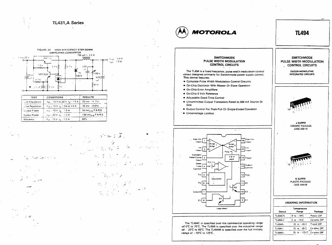
The IC TL494 is used to control the current through motor windings.
Features:
fixed frequency PWM control circuit designed for switch mode power supply
control
on chip oscillator
on chip error amplifier
output transistors rated at 500mA source or sink
The TL494 is used to provide a stable current in the windings of the motor as small
changes in the current changes the position of the motor. Th$ current stability is better
in a linear regulator, but in a chopper, the power efficiency is better, with a good
current stability. The output of the PWM is compatible to the TTL logic levels, making
it easy to control the driver. Four such modulators are used, one for each winding of
the two motors.
The output of the DAC is given as the reference voltage to the error amplifier. The
current in the driver is sensed(by a sense resistor) and fed to the error amplifier to
generate the PWM o/p in the proper sense.
When the f/b voltage from the sense resistor is greater than the reference
voltage (from DAC) to the error amplifier of the PWM duty cycle of the PWM
decreases. Similarly when the f/b voltage is lesser, duty cycle increases. When the
motor has been latched to a particular position, the PWM helps in maintaining a
constant average output voltage by correcting errors and varying the duty cycle at the
output depending on the feedback.
The response of the PWM also depends on the gain of the error amplifiers.
Very high gain makes it to respond to small changes at the reference of the feedback
making the putput unstable. So an optimum gain is to be designed. Further a suitable
series RC element is added to the FIB of the error amplifier to reduce the noise in the
motor.
Dept. of Electronics & Cotnmunication,B J.T.,1996-97

Hardware
Design:
- One of the error amplifiers is disabled.
- The output transistors of TL494 are used in parallel to provide current to the driver.
- Dead time control and output control pins are disabled.
- The modulator is operated at 25KHz .The RT and CT are suitably selected by using
the formula -
Fosc = 1.1
RT . CT Assuming CT=10 KpF, we get RT= 4.7KSL
Error Am. pli fier Design :
Gain = 3 3 0 K / 1 . 2 K @ 330&
!
Figure 2.4.1
The output along with SQ(as shown below) is fed to the driver through a digital circuit
which decides the direction of current.
Dept. of Electronics & Cornm unication,B.l.T.,1996-97
PWM O/P
SQ DRIVER
PWM O/P
SQ
CURRENTS
b TO
b
F MOTOR
L298

Hardware
2.5 DRIVER
A digitally controllable driver is used to control the direction and the magnitude
of the current in the windings. The driver used in this application is the Dual Full-
Bridge Driver L298. It is a power integrated circuit usable for driving resistive and
inductive loads. This device has four push-pull drivers with separate logic inputs and
two enable inputs. Each driver is capable of driving loads up to 2A continuously. The
maximum operating voltage for the driver is 50V.
The emitters of the low-side power drivers are separately available for current
sensing. Feedback from the emitters can be used to control load current in a switching
mode or to detect load faults.
Separate logic and load supply lines are provided to reduce total IC power
consumption. It is further reduced when enable inputs are low.
Two such drivers are employed, one for each motor. Each full bridge has one
phase winding(inductive load) of the motor as the load i.e., A or B. The drivers are
enabled by ENA and ENB for frequency and power motors respectively.
Power supply given = 20V
As mentioned earlier the full scale voltage to a winding is 1V. If a full scale current of
330mA is desired in each winding, high wattage sensing resistors of 3.3Q each is
used.
A single heat sink is provided for both the drivers.
The current is passed through the windings by turning on a pair of diagonally
opposite transistors. As mentioned before, the PWM o/p along with SQ signal is used
to turn ON the appropriate pair of transistors(Ql,Q4 or Q2,Q3) to change the
direction of the current, as shown in the fig. 2.5.l(shows the circuit for one of the 2
windings). Flywheel diodes provided across the transistors are required to maintain the
direction of the current in the inductive load when the transistors are switched at a high
speed by the control from the PWM.
The voltage across the sensing resistance connected to the drivers changes polarity. It
has to be rectified before feeding it to the PWM error amplifier. Since the amplitude of
Deut. o f Electronics and Communication, B.I.T. . 1996-97 21

the sensed voltages are very low, 11igh precision rectification is required. LF347 ,a
quad high-speed JFET operational amp1 ifier.
This is done by the rectifier :IS shown in fig.2.5.2
r?
f r o
F i g u r e 2 . 5 .1 I n t e r n a l s t r u c t u r e o f L238C1 o f 2 3
R
F R E C I S I O N R E C T I F I C A T I O N
R E C T I F I E D O / F
C V f / b t o P W M I

Hardware
2.6 STEPPER MOTOR:
Stepper motors are used to vary the position of the p-meters. This is done by
coupling the motor shaft to the p-meter. The available stepper motor is HY200-1713-
033BC horn SGST which is a 2-phase motor with 200 full steps.
This particular motor will require a driver with voltage and current rating of
about 15V and 330 mA per phase. Also to be noted is the fact that 200 stepslrev
stepper motors are commonly available in the market.
From the frequency and power position charts for three Gunn oscillators, we
find that for a 1GHz change in frequency, a minimum rotation of 0.7 mils is required at
the highest frequency. In our application, a resolution of 10MHz is required, which
corresponds to a rotation of 0.007 mils.
1 rotation corresponds to 25 mils -200 full steps
0.007 mils -+ 1/18 of a full step
Therefore the stepper motor has to be used in p-stepping mode resulting in a
minimum of 3600 steps per revolution. Five bits are used provide signals to the driver. So
a total of 32 microsteps may be obtained in one full step. A total of 6400 micro steps per
revolution is obtained which is greater than the requirement.
This motor has six leads and two phases(as shown in data sheet). Each phase has
two windings in series. Either of the windings may be used with the common lead, or
both the windings in series. In this application only one winding has been used in order
to reduce the current drawn. If both were to be used, the supply voltage has to be
increased from 16V to a greater value.
A DC motor with gears would have served the purpose but since it had to be
imported, a stepper motor is suitably used.
Dept. of Electronics & Comazunication, B.I.T.,1996-97
Hardware
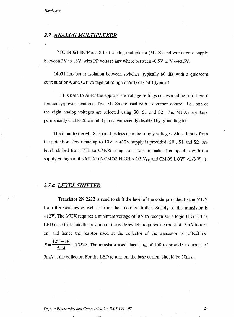
2.7 ANALOG MULTIPLEXER
MC 14051 BCP is a 8-to-1 analog multiplexer (MUX) and works on a supply
between 3V to 18V, with I/P voltage any where between -0.5V to VDD+0.5V.
14051 has better isolation between switches (typically 80 dB),with a quiescent
current of 5nA and O/P voltage ratio(high onloff) of 65dB(typical).
It is used to select the appropriate voltage settings corresponding to different
frequencylpower positions. Two MUXs are used with a common control i.e., one of
the eight analog voltages are selected using SO, S1 and S2. The MUXs are kept
permanently enabled(the inhibit pin is permanently disabled by grounding it).
The input to the MUX should be less than the supply voltages. Since inputs from
the potentiometers range up to 10V, a +12V supply is provided. SO , S1 and S2 are
level- shifted from TTL to CMOS using transistors to make it compatible with the
supply voltage of the MUX .(A CMOS HIGH > 213 Vcc and CMOS LOW 4 1 3 Vcc).
LEVEL SMFTER
Transistor 2N 2222 is used to shift the level of the code provided to the MUX
from the switches as well as from the micro-controller. Supply to the transistor is
+12V. The MUX requires a minimum voltage of 8V to recognize a logic HIGH. The
LED used to denote the position of the code switch requires a current of 5mA to turn
on, and hence the resistor used at the collector of the transistor is 1.5KQ i s .
12v - 8V R = = 1.5KQ. The transistor used has a hfe of 100 to provide a current of
5mA
5mA at the collector. For the LED to turn on, the base current should be 50pA .
Dept of Electronics and Communication B.I.T 1996-97

Hardware
The base of the transistor is connected to the micro-controller , the minimum
logic HIGH voltage from the controller is 2.5V. Hence, for the base current to be
50pA, a 33KQ resistor is used, talang into account the 0.7V drop at the transistor, i.e.
The code switches are connected to the controller through a 3KQ resistor.
This is to provide appropriate voltages ( logic HIGH ( min ) =2.5V, logic LOW (max)
= 0.7V ) at the controller pins and also to provide appropriate current ( 50 pA ) to the
base of the transistor to turn on the LED at the collector when the switch is in the ON
position (logic HIGH). A HIGH at the i/p of the level shifter appears as a LOW at the
olp, and vice-versa, because the transistor acts as an inverter. Due to this, the order of
selection of the reference pots is inter-changed. I -- - -
L - - - - .
FROM C O N T R O L L E R 33Kh iNPN>" 2 N 2 2 2 2
L.., FROM S W I T C H
I L E V E L S H P F T E R
Figure 2.7.1
The output of the MUX is given to the comparator(inverting terminal).
LM339 is the comparator used. These are high-precision comparators which
eliminates the need for dual supplies and are compatible with all logics. The selected
voltage is compared with the voltage from the feedback potentiometers coupled to the
motors. This voltage represents the instantaneous position of the motor. The
comparator output (to be more precise, the transition from one logic level to another)
is given to the micro-controller(CW.6 and CW.7) through pull-up resistors.
Dept of Electronics and Communication B.I. IF 1996-97
Hardware
There are eight reference pots for motor 1. The voltage on each pot
corresponds to one of eight frequently used values of frequency in the Gunn oscillator.
A similar set of voltage levels are adjusted for the eight pots corresponding to motor
2. Each voltage selects a particular power for the oscillator. The signals of each
frequency have to have a pre-determined power, and so the frequency and power of
the signals have to be simultaneously set to the desired value.
The values of So, S1 and S2 determine the reference pot selected as the output of
the MUX. This olp is continuously compared with the varying voltage from the
feedback potentiometer, and when the feedback voltage equals the reference voltage,
there is a transition of logic level ( H+L or L+H ) at the comparator olp which is
being monitored by the micro-controller. When such a transition is detected, the
controller freezes all data to the DACs and as a result, the motor currents are stabilized
(remains constant) . The motor is then fixed at the present position , setting the
oscillator to the required frequency 1 power.
2.7. b INDICATORS :
There are five LEDs on the main board. Three of them indicate the status of the
code pins S2, S1 and So. The other two indicate whether the two motors are on or off.
A special feature included in the software is to indicate when the motor has stopped
moving, either after being set to the desired position ( after doing coarse movement )
or after the motor has been manually stopped ( while doing fine movement, and the
STARTISTOP bit is made LOW ). The indication is given by making the code LEDs
blink for a short duration ( 10 seconds ).
NOTE: Since the blinking is generated by toggling the inputs to the transistors used
for level-shifting, if the code happens to be (0,0,0) , the Ups are permanently LOW as
seen fromfigure 2.7.1 and hence the LEDs do not blink.
Dept of Electronics and Communication B. I. T 1996-97 I

Hardware
2.8 POWER SUPPLY REQUIREMENTS:
The unregulated supply given is +I- 16V. These voltages are regulated by ICs
7812 and 7912 to provide +I-. 12V. A 5V regulated supply is obtained in the second
PCB using IC 7805. On the 1" PCB, a reference voltage generator AD581 is used, to
get a stable reference voltage of 10V .
The current drawn by the PCBs from the +12V supply is around 175mA, and
from the -12V supply it is around 50mA
The current drawn by the +5V regulator (7805) alone, on the 2nd PCB is
around 75mA. The power dissipation in the regulator is reduced by connecting a
resistor in series, the value of which is chosen to be 82 ( 1W )such that 8V appears
at the i/p of the regulator. Suitable heat sinks are provided for all the regulators.
Since the entire system is powered ON always, to reduce the power
consumption, HCT ICs are used.
Dept of Electronics and Communication B.I.T 1996-97
.. ?..

Hardware
2.9 REFERENCE DESIGN.-
The maximum current that can be drawn from the reference AD581 is 10mA.
This current is not sufficient for the various references required. Suitable buffers
(LM324) limit the current to 5mA and also provide appropriate voltages to various
devices as mentioned below.
DAC : 4 DACs are used . These require a current of 2mA and a voltage between 0
and 10V. Hence a 5KR pot is used at the ilp of the LM324 .
2 FIS POTS OFREO/POWER): The f/b POTS require supply of 10V and current of
1mA each , to provide good resolution to sense the voltage change with each micro-
step . Hence, lOKR pots are used.
16 REFERENCE VOLTAGE POTS (8 -FREO. &POWER): ~ a c h ' o f the POTS
used for setting reference voltages for selecting different frequencies require a current
of 1.6mA and a voltage between 0-10V. Hence, a pot of 5KR is used at the i/p of the
LM324 .
The pots used for setting voltages for selecting different power values
corresponding to each frequency setting require a current of 1.6rnA and a voltage of
10V each.
The power p-meter has more number of turns than the frequency p-meter. So
the range of reference voltages is greater. Hence higher value potentiometers of 50KQ
are used.
Dept of Electronics and Communication B.I.T 1996-97

Hardware
2.10 INTERRUPT CONTROL :
Limit switches are provided to indicate if the p-meters have reached their
extreme position. The configuration for this is as shown in the schematic diagram.
Here, when the p-meter reaches its limit, the limit switch will be hit. The controller
will be interrupted when the limit switch is hit, OR when the fuse blows after an excess
current flow due to a fault. This in turn results in an interrupt subroutine being
executed to disable the drivers. The status of the two limit switches ( freq. motor 1
power motor ) is also available to the controller through the control word , based on
which appropriate action can be taken i-e., two bits are assigned to indicate the status
of each p-meter. These bits are cleared when the corresponding motor has reached its
limit .
Interrupt circuit design:
To provide a voltage of 3V at the i/p of the NAND gate, a voltage divider
circuit is provided, as shown by the figure. To provide a current of 5mA to the LED, a
resistor of value 2.7Ka is connected in series with the LED.
VCC41VCC5 D R I V E R SUPPLY
A 2.7K 12K
2.7K L E D
? I
NAND sate
Figure 2-10. d
Dept of Electronics and Conzmunication B.I. T 1996-97
Hardware
2.11 SERIAL COMMUNICATION=
When the two motors are to be operated from a distant location, say from a
P.C. , the L R pin is maintained at HIGH. A separate program is run from the P.C. side
to do the following:
a) Set up the required baud rate
b) Send data serially to the p-controller to set frequency or power
c) Send or receive acknowledgement tolfrom the controller
Similarly, at the controller side, when the L R pin is HIGH, a routine monitors
the data at the serial pin Rx of the controller, and suitably processes it to make the
necessary changes, i.e. set frequency1 power as desired, or send an acknowledgement
signal back to the P.C.
The baud rate to be used for transmission is to be specified by setting up a
counter (timer 1) in auto-reload mode with a specific count corresponding to the baud
rate required. The baud rate used in our application is 9600 baud @its per sec ) . For
this purpose, all timer interrupts have to be disabled.
If the control system is running in the LOCAL mode, with TR pin at LOW,
and if a remote P.C. tries to access the p-controller, the serial interrupt of the 803 1 is
activated, and the controller then performs an interrupt service routine which sends a
message to the P.C. that the controller is currently being used in the LOCAL mode and
cannot be accessed by the P.C.
2.11.a SERIAL INTERFACE:
Serial communication with a PC for remote mode of operation is performed using
the in-built UART. Rxd and Txd levels are shifted to RS-232 interface standard with
the help of a chip ICL 232.
Chip details:
ICL 232 is a, dual RS-232 transrnitter/receiver interface circuit that meets EL4
RS-232 specifications with TTL ! CMOS compatibility and low power consumption.
Dept of Electronics and Communication B.I. T 1996-97

Hardware
The logic levels may be shifted between
logic 1 -+ -12V
logic 0 -. +12v
The serial interface may be schematically represented as shown.
Serial port of P.C.(COMl/COM2) may be used. This may also be
implemented in Daisy Chain mode where the master accesses several slaves each with
a different address, where the controller may be one of them. Suitable settings are
made in the system BIOS for communication.
RS 232 Port of
Controller (Slave)
The UART in the p-contl-oller can be operated in different modes:
Mode 0: 8 data bits at fixed baud rate
Mode 1: 10 bits ( 8 data + 1 start + 1 stop) at variable baud rate
Mode 2: 11 bits( 8 data + 1 start + 1 stop + 1 programmable bit ) at fixed baud
rate.
Mode 3: 11 bits ( 8 data + 1 start + 1 stop + 1 programmable bit ) at variable baud
rate.
h ( 2 ) Tx(3:l 4
Tx(3) Rx(z (5) Grid (7)
Mode 1 and Mode 3 is used in this application so as to use the variable baud
rate.Mode 3 has a programmable gth bit. The gth bit may be used to indicate whether
the byte is an address byte or a data byte. The 9"bit is set to 'I7 by setting the bit TBS
in the SCON register. RBS corresponds to ninth received bit.
gth bit is ' 1' -+ Address byte
9" bit is '0' +- Data byte
serial port of P.C.
(Master)
Dept ofElectron,ics and Commrinicn.tion B.1.T 1996-97

Hardware
2.12 HARD WARE CORRECTIONS: 7,
1. In the PCB, the bit positions had been reversed by mistake. Since the lower 3
bits of the DAC were shorted to ground , the data byte provided to the DAC from the
controller was changed ( by modifications in the software ) in such a way as to keep
the byte unaltered as seen from the DAC .
The full-scale voltage at the output of the DAC had to be scaled down to the
design value of lV, for which the value of the resistor RL was re-designed as shown
below.
5V 255 1V Where Rref = 2.2 KO I=- X---
2.2M1 256 - 470R R, = 470R
2. One of the error amplifiers of the PWM had to be disabled by giving the
reference olp ( pin 14 ) of PWM to it's inverting terminal ( pin 15). Instead, it was
connected to non-inverting terminal ( pin 16 ) . This was corrected on the board as
desired.
3. The path ADO was missing on the PCB . An external link is provided .
Dept of Electronics and Communication B.I. T 1996-97


SOFTWARE:
The software includes writing an assembly language program for the 8031
micro controller and C++ programming at the PC end for serial communication.
The Assembly Language Program (A.L.P.) is explained with flow charts.
3.1 Program Description:
In the main program, the control word along with the code settings is read and
stored in the beginning and depending on the position of the LOCAL 1 REMOTE
switch ( LOW I HIGH ), the program jumps to local or remote routines. In the
LOCAL routine, no action is taken till the START I STOP switch is set .On start, the
code settings are compared with the previous value; if they are the same, control is
passed on to the fine movement routine of the motor ( Frequency or power motor
depending on the position of the FREQ I POWER switch ) . If the code settings are
different, control is passed to the coarse routine . Here the power motor is moved
after the frequency motor . In the course of movement of the frequency motor, if the
START 1 STOP switch is cleared, control is passed back to the main program without
doing the power routine. Otherwise, the motor is rotated till there is a transition in
the comparator olp ( i.e., the motor reaches the desired position ) and the control is
passed to the power routine in which the same procedure is followed . After the
power motor has reached the desired position, or the START I STOP switch is
cleared, control is transferred to the main program .
In the coarse routine, to indicate the stopping of the motor, a blink routine is
called, which toggles the code LEDs for a duration of l0sec.
In the remote mode of operation, the controller continuously polls for the data
to be received. A link is established between the P.C. and the controller by sending an
address to the controller. If the address from the P.C. is valid? the controller L
acknowledges by sending an acknowledge signal to the P.C. along which information
regarding the latest code set in LOCAL, the status of and lirnit switches are sent.
If the controller is in LOCAL mode, then no further information is sent to it from the
P.C. side. Else, a second byte is transmitted. The P.C. polls for the acknowledgement
only for a certain interval of time after which the address has to be re-transmitted if
Dept of Electronics And Communication B.I.T., 1996-97

Software
required. Once the link is established, the second byte is transmitted This carries
information about the code set from REMOTE, the motor to be operated, the direction
of operation(if it is fine movement another byte indicating the number of steps may be
sent). The controller processes the data and moves the motor accordingly. After
completion of operation, another acknowledgement is sent to the P.C.
The data transmission is mainly in polling mode at both the ends. Eleven bit
operation is employed for the transmission of the address byte. Apart from the start,
stop and 8 address bits, a ninth bit is set which identifies the byte as an address, to the
controller. ( mode 3 operation). The P.C. employs 1 1 bit operation by using 2 stop
bits for transmission. One of the stop bits is interpreted as the ninth data bit by the
controller. After the address is acknowledged and the link is set up, both the P.C. and
controller change to 10 bit operation.(mode 1 operation ).
REGISTER INITIA LIZA TIONS:
The pointers for the look-up tables are stored into registers at the beginning of
the program. Some special function registers have to be initialized at the beginning of
the program. They are described as follows:
TCON: Timer 1 Counter Control Register
TCON is set to 40H , thereby turning timer 1 on to generate the required baud
rate for serial communication. Level triggering mode is used for interrupt INTO.
TMOD: Timer 1 Counter Mode Control Register
TMOD is used to enable either timer or counter operation and to set their
mode of operation. Among the 8 bits, 4 bits each are used to set parameters for each
timer (Timer 0, Timer 1). Timer mode is enabled, and the timer ( Timer 1) is operated
in mode 2 , which is an 8-bit auto reload mode. This is done to generate the required
baud rate. TMOD is set to 20H. The 8-bit reload value to set the baud rate is stored
in TH1 and TL1.
Dept of Electronics And Communication B .I.T., 1996-97

Baud rate is generated(M0de 1 and 3) using the relation
2 sMoD Osc. freq X
32 12 x (256 - TH1)
where oscillator frequency is 11.059MHz, SMOD = 0 and THl=FDH
which is the reload value. A value of FDH is used for a baud rate of 9600bps.
PCON: Power control Register: This register is set to OOH and is redundant in this
application.
SCON: Serial Port Control and Status Register.
This register contains not only the mode selection bits , but also the 9th data
bit for transmit and receive ( TB8 and RB8 ) and the serial port interrupt bits ( TI and
.
SCON is set to 58H for Mode 1 and D8H for Mode 3 respectively. Both have
variable baud rate: TI and RI are polled for transmission and reception of data.
IE (Interrupt Enable Register):
IE is set to 91H in LOCAL mode to enable interrupt INTO and serial interrupt
and 81H in REMOTE . Serial interrupt is used only in LOCAL mode to deny the
remote access since the controller cannot poll serial reception in this mode.
On the P.C. side, a built-in function of C++, BIOSCOM is used to define
settings for baud rate and to read the status register after each transmission and
reception. It also defines the port to be accessed (COMllCOM2). Functions inportb
and outportb are used to receive and send data respectively. Details of setting serial
port configuration from BIOS is given in the data sheets.
The ALP is converted to object code using assembler X8051. The OBJ file is
converted to HEX file using LINK51 which is further converted to a binary file by
HEXBIN converter. This binary file is programmed on to the EPROM using
CHIPMASTER 3000.
Dept of Electronics And Communication B .I.T., 1996-97

Flowcharts for software at the controller
POWER ROUTINE
Dept of Electronics And Communication B .I.T., 1996-97

FREQUENCY / POWER ROUTINE 0 READ COMPARATOR VALUE AND )I
Dept of Electronics And Communication B.I.T., 1996-97

Software
v
READ CONTROL WORD
REVERSE FINE
FINE ROUTINE FOR FREQ / POWER
Dept of Electronics And Communication B .I.T., 1996-97

Software
Initialise SFRindicating the baud rate and mode of operation for 11-bit operation
1 S E T
I RECEIVE ADDRESS BYTE I VALID
ADDRESS ?
I SEND ACKNOWLEDGEMENT BYTE I I I TRANSMITRECEIVEDBYTE I
1 ~0 FOR Tl
/ \ ( MAIN 1 1 zz 2nd BYTE
I RECEIVE DAT A BYTE I
Dept of Electronics And Communication B .I.T., 1996-97

Software
1 ~0 FOR TI
Dept of Electronics And Communication B .I.T., 1996-97
INTERRUPTS
EXTERNAL INTERRUPT
DISABLE DRIVERS
w
T O MAIN Cxl SERIAL
INTERRUPT
v
T RAN SM IT STATUS
RETURN a

PC COMMSJNICATION FLOWCHART FOR PROGRAM AT THE P.C.
I SET UP SERIAL COMMUNICATION PARAMETERS I
I SELECT FREQUENCYiP OW ER T 0 BE SET I
I SEND ADDRESS BYTE T O CONTROLLER I
Dept of Electronics And Communication B.I.T., 1996-97


Conclusion
CONCL USION
The present work has presented a study in the electronics of a stepper motor, using a p-controller ( 8031 ) as the Central Processing Unit. The main aim of the project is to control a 200-step stepper motor in p-stepping mode to get 3600 steps per revolution, each step corresponding to a change of 0.3 mV on the coupled f/b pot.
The system operates the motor in both coarse and fine movement.
Coarse movement by setting a code ( S2, S1, SO ) on the front panel. The motor moves only if the code sent varies from the previously stored value, and in a direction determined by the code and the comparator o/p.
To comparator
MOTOR - COUPLTNG Pot Reference Direction of DEVICE
Observation
H -+ L transition * Anti-clockwise movement L -+ H transition Clockwise movement
The direction of rotation may be changed by either making alterations in the software, or by reversing the polarities of the f/b pots.
Fine movement by setting the direction switch on the front panel, and turning the motor ON and OFF by using the START /STOP switch on the front panel.
DIRECTION SWITCH: L - Clockwise inovenlent H -. Anti-clockwise movement
For the purpose of testing, 8 different voltages were set at the reference pots, one for each freq/power. On setting a particular code, the motor moved to the specified postion wherein the f/b voltage equalled the reference i/p. All the codes were set one by one, and in each case, after the motor stopped moving, the readings corresponding to the f/b voltages and reference voltages were measured using a 5-digit multimeter ( to observe changes of the order of mV).
A plot of the code v/s f/b voltage indicated that the readings coincided for both forward and reverse direction of motor movement.
Dept. of Electronics and Coininunication, B.I. T. ,1996-97

Conclusion
The differences b/w the reference and f/b voltages were tabulated, and a plot of the differences v/s code revealed that the deviation for all codes was fairly constant for L-H transitions, i.e., clockwise movement of the motor, at a value of 0.5mV. This corresponds to an error of 3 p-steps. This problem can be solved by providing a suitable off-set in the reference voltages corresponding to each code, or by moving the motor in fine movement after the motor has stopped.
In remote operation, the motor movements can be controlled from a distant location, by a P.C.
The P.C. can set the required freqlpower and transmit the code to the controller. The P.C. first sends an address byte to the controller, and sends the code as a data
byte only on receiving an acknowledgement. The controller gives an indication to the P.C. when the motor has reached the desired
position, and also gives information regarding the status of the controller. When the P.C. tries to access the system when it is operating in LOCAL mode, the
controller gives an indication to it, denying permission to change settings. A facility can be provided to operate the motor in fine movement. For this purpose,
the software at the P.C. side can be modified to send a 2nd data byte containing the no. of steps to be moved, and in what direction.
A hot-key can be provided at the PC to stop motor movements immediately, if the key is pressed.
Dept. of Electronics and Communication, B.I.T. ,1996-97


Appendix
PHOTOGRAPHS :
FRONT VIEW OF THE MODULES
Dept of Electronics & Communication B.Z.T., 1996-97

9 VIEW ,- OF PCB I . --.-
VIEW OF PCB 2
Dept of Electronics & ~ornrnunication B.I.T.,1996-97

Appendix
C O H P R R R T O R O / P T O P C 8 2 ( 1 O f 5 1
U N R E G U L H T E D S U P P L Y T O P C B 2
3 P C R P
iii Dept of Electronics & Communication B.Z. T.,1996-97

Appendix
Dept of Electronics & Communication B.I. T.,1996-97

Appendix
Dept of Electronics & Communication B.Z. T.,1996-97

Appendix
Dept of Electronics & Communication B.Z.T.,1996-97

Appendix
B O T V M
B 1 C O M P
0 1 C O M P
4 - 5 I Q U T
vii Dept of Electronics & Communication B.I. T.,1996-97

Appendix
V l - V 2 -
O / P R E F D / P
V P - V 2 -
O / P A E F O / P
V 1 - v 2 -
O / P R E F I ) / P
V 1 - V 2 -
O / P R E F O / P
F E E D B A C K
Dept of Electronics & Communication B.I. T.,1996-97 viii

Appendix
1 A 2 1 Y 2
2 A l 2 Y 1 2 R 2 2 Y 2
I 3 O F 5 1
2 A B 2 Y l Z R 2 2 Y 2
I E N P E
E N A B L E 1 o f 5 )
Dept of Electronics & Communication B.I.T.,1996-97

Appendix
p U H a
CND
Dept of Electronics & Communication B.I.T.,1996-97

Appendix
Dept of Electronics & Communication B.Z. T.,1996-97


Appendix
Dept of Electronics & Communication B.I. T.,1996-97 xiv

Appendix
Dept of Electronics & Communication B.I. T.,1996-97

Appendix
LIST OF COMPONENTS OF PCB-1 Reference Settings and Regulators
Item Quantity Reference Part
Cl ,C2,C3,C4 C5,C6,C9,ClO,Cll ,C14 3T CAB C7 .33uf C8 33uf C12,C13 .Oluf/l6V D2,Dl LED F1 ,F2 FUSEI25OmA JP3, JP 1 HEADER 3 JP4, JP2 HEADER 2 JP5 HEADER 4 R1 ,R2 1.8K U1 EM339 U2,U3 MC14051 U6 UA78 12UC U7 UA79 12UC JP9, JP6 HEADER 10 JP7, JP8 HEADER 3 R l 17R13,R14,R15,R16,R17, 10K R18,R R3,R4,R5,R6,R7,R8,R9,RlO 50K R19,R207R21 5K U5 IN324 US AD58 1
ConnectorsIHeaders JP1 Codes from PCB 2 JP2 Comparator olp to PCB 2 JP3 Supply JP4 Unregulated supply to PCB 2 JP5 Regulated supply to PCB 2 JP6 Monitoring power reference values JP7 To power feedback pot JP8 To frequency feedback pot JP9 Monitoring frequency reference values
Dept of Electronics & Communication B.I. T.,1996-97 xvi

Appendix
LIST OF' COMPONENTS OF PCB-2 Controller
Item Quantity Reference Part
. luf
.O lufIl6V 22ufl25V DIODEIswitch DIODE ZENER LED DIODEIFR 102 '
DIODE FUSEl500mA CON9 HEADER 2 HEADER 4 ' HEADER 18 E r n I E R 3 I E N I E R 6 2N2222 470 4.7K
Dept of Electronics & Communication B.Z. T.,1996-97

Appendix
8.2K 33K 1.8K 12K 3.311w 1.5K 8211 W SW DPDT SW SPDT ICL232 UA7805UC TL494RRI LF347RRI 7404 74HCT23 8 74HCT573 80C31 BH DAC0800
AM27C64 74HCT244 LM324 7400 7408 k298
CRYSTAL(11.0592Mhz)
J1 RS 232 Connector J6 Codes to PCB 1 J2 Supply to Driver 1 J7 Comparator olp fromPCB l J3 Supply to Driver 2 J8 Unregulated supply from PCB 1 J4 Regulated supply from PCB 1 J9 To motor 1 J5 Front panel switches J l0 To motor 2
Dept of Electronics & Communication B.I.T.,1996-97

Bibliography:
Intel Component Data Catalog
Intel 8-bit Embedded Controller
RCA High-speed CMOS Logic ICs ( Harris Semiconductor )
Linear Data Book ( National Semiconductor Corporation )
Data Conversion Products Data Book ( Analog Devices )
Operational Amplifiers - Design and Applications ( Burr - Brown )
PC Systems Programming ( Abacus )

8031/8051/8751 SINGLE COMPONENT 8-BIT MICROCOMPUTER
IU 8031 - Control Oriented CPU With RAM and 110 8051 - An 8031 With Factory Mask~Programmable ROM
H 8751 - An 8031 With User ProgrammablelErasable EPROM
H 4K x 8 ROMIEPROM 1 2 8 x 8 R A M
m Four 8-Bit Ports, 32 110 Lines Two 16-Bit TimerlEvent Counters
E High-Performance Full-Duplex Serial Channel External Memory Expandable to 128K
H Compatible wi th MCS-8U@lMCS-85@ Peripherals
Boolean Processor m MCS-48@ Architecture Enhanced with:
Nan-Paged Jumps Direct Addressing Four 8-Register Banks
* Stack Depth Up to 128-Bytes Multiply, Divide, Subtract, Compare
&?i Most Instructions Execute in I p s - ap 4ys Multiply and Divide
The Intel@ 8031/8051/8751 is a stand-alone, high-performance single-chip computer fabricated with Intel's highly-reliable +5 Volt, depletion-load, N-Channel, silicon-gate HMOs technology and packaged in a 40-pin DIP. It provides the hardware features, architectural enhancements and new instructions that are necessary to make it a powerful and cost effective controller for applications requiring up to 64K bytesof program memory and/or up to 64K bytes of data storage.
The 005118751 contains-a non-volatile 4K x 8 read only program memory; a volatile 128 x 8 readlwrite data memory; 32 1/O lines: two 18-bit timer/counters: afive-source, two-priority-level, nested interrupt structure; a serial I/O port for either multi-processor communications, I/O expansion, or full duplex UART; and on-chip oscillator and clock circuits. The 8031 is identical, except that it lacks the program memory. For systems that require extra capability, the 8051 can be expanded using standard TTL compatible memories and the byte oriented MCS-80 and MCS-85 peripherals. The 8051 microcomputer, like its 8048 predecessor, is efficient both as a controller and as an arithmetic processor. The 8051 has extensive facilities for binary and BCD arithmetic and excels in bit-handling capa- bilities. Efficient use of program memory results from an instruction set consisting of 44% of one-byte, 41% two-byte, and 15% three-byte instructions. With a 12 MHz crystal, 58% of the instructions execute in lps, 40% in 211s and multiply and divide require only 4ps. Among the many instructions added to the standard 8048 instruction set are multiply, divide, subtract and compare.
RSTlVPD
COUNTERS
INTERRUPTS
Figure 1. Block Diagram
Figure 2. Logic Symbol
(L
Figure 3. Pin Configuration

ABSOLUTE MAXIMUM RATINGS*
Ambient Temperature Under Bias ... .O°C to + 70°C
Storage Temperature .......... - 65°C to + 150°C
Voltage on any Pin to VSS.. .............. -0.5'4 to VCC +0.5V
Voltage on Vcc to VSS ............. -0.5V to 6.5V
Maximum loL per I/O pin ................. .15 mA
Power Dissipation. ....................... .1 .OW* 'This value is based on the maximum allowable die temperature and the thermal resistance of the package.
D.C. CHARACTERISTICS (TA = o°C to 70°C; Vc
Symbol Parameter Min Typ(3)
lnput Low Voltage (Except m)
VIH Input High Voltage 0.2 VCC + 0.9 (Except XTALI , RST)
VIHI / Input High Voltage 0.7 VCC (XTAL1, RST)
Output Low Voltage (6) (Ports 1,2,3)
(Port 0, ALE, m)
(Ports 1.2.3, ALE, m) 0.75 VCC
VOH1 Output High Voltage (Port 0 in External Bus Mode)
0.9 Vcc
Logical 0 lnput Current (Ports 1,2,3)
Logical 1 to 0 Transition Current (Ports 1,2,3)
-p
1 LI Input Leakage Current (Port 0, EA)
RRST Reset Pulldown Resistor 50
CIO Pin Capacitance
I cc Power Supply Current: Active Mode, 12 MHz (4)
Idle Mode, 12 MHz (4) Power Down Mode
*Notice: Stresses above those listed under 'Ybso- lute Maximu.m Ratings" may cause permanent dam- age to the device. This is a stress rating only and functional operation of the device at these or any other conditions above those indicated in the opera- tional sections of this specification is not implied Ex- posure to absolute maximum rating conditions for extended periods may affect device reliabi/ity.
NO TlCE Specifications confained within the following tables are subject to change.
c = 5v +20%; vss = OV)
Max Unit Teat Conditions
0.2 vcc -0.1 v
150 KR
10 pF Test Freq = 1 MHz, TA = 25°C

2764 (8K x 8) UV ERASABLE PROM
200 ns (2764-2) Maximum Access Pin Compatible to 2732A EPROM Time . . . HMOs*-E Technology
Industry Standard Pinout.. . JEDEC Compatible to High Speed 8mHz Approved 8086-2 MPU . . . Zero WAlT State
Low Active Current ... 100mA Max. Two tine Control
The Intelm 2764 is a 5V only, 65,536-bit ultraviolet erasable and electrically programmable read-only memory (EPROM). The standard 2764 access time is 25011s with speed selection available at 200ns. The access time is compatible to high performance microprocessors, such as Intel's 8mHz 8086-2. In these systems, the 2764 allows the microprocessor to operate without the addition of WAlT states.
An important 2764 feature is the separate output control, Output Enable (e) from the,Chip Enable control (CE). hem control eliminates bus contention in multiple bus microprocessor systems. Intel's Application Note AP-72 describes the microprocessor system implementation of t h e m and- controls on Intel's EPROMs. AP-72 is available from Intel's Literature Department.
The 2764 has a standby mode which reduces the power dissipation without increasing access time. The active current is 150mA while the standby current is only 50mA. The standby mode is achieved by applying a TTL-high signal to the @E input.
The 2764 is fabricated with HMOs'-E technology, Intel's high-speed N-channel MOS Silicon Gate Technology.
BLOCK DIAGRAM
DATA OUTPUTS VCC - 0 0 - 0 7 CND -
OUTPUT BUFFERS f5- PROG LOGIC
h3-A.2
ADDRESS INPUTS
2732A PIN CONFIGURATION
MODE SELECTION
x can be either V,, or V,,
PIN CONFIGURATION
A l l - OE
0 5
[ I ] For total compatibil~ty and upgradabillty from the 2732A and ROMs provide a trace to pin 26.
PIN NAMES
CHlP ENABLE OUTPUT ENABLE
0 -0, OUTPUTS PGM PROGRAM
NO CONNECT
'HMOs is a patented process of Intel Corporation.

ZRASURE CHARACTERISTICS Standby Mode
The erasure characteristics of the 2764 are such that erasure 3egins to occur when exposed to light with wavelengths shorter than approximately 4000 Angstroms (A). It should be noted that sunlight and certain types of fluorescent lamps have wavelengths in the 3000-4000 A range. Data show that constant exposure to room level flclorescent lighting could erase the typical 2764 in approximately 3years, while it would take approximately 1 week to cause erasure when exposed to direct sunlight. If the 2764 is to be exposed to these types of lighting conditions for extended periods of time, opaque labels are available from lntel which should be placed over the 2764 window to prevent unintentional erasure.
The recommended erasure procedure for the 2764 is expo- - sure to shortwave ultraviolet light which has a wavelength of
2537 Angstroms (A). The integrated dose (i.e., U V intensity X exposure time) for erasure should be a minimum of 15 W-sec/cm2. The erasure time with this dosage is approxi- mately 15 to 20 minutes using an ultra\riolet lamp with 12000 pW/cm2 power rating. The 2764 should be placed within 1 inch of the lamp tubes during erasure. Some lamps have a filter on their tubes which should be removed before erasure.
DEVICE OPERATION
The five modes of operation of the 2764 are listed in Table 1 . A single 5V pomer supply is required in the read mode. All inputs are TTL levels except for Vpp.
TABLE 1. MODE SEL.ECTION
x can be either V,, or V,,
READ MODE
Outputs (1 1-13, 15-1 9)
DO",
HighZ
DIN
Do",
High Z
Read
Standby
Program
Program Verify
Program Inhibit
The 2764 has two control functions, both of which must be logically satisfied in order to obtain data at the outputs. Chip Enable (CE) is the power control and should be used for device selection. Output Enable (OE) is the output control and should be used to gate data to the output pins, indepen- dent of device selection. Assuming that addresses are stable, address access time (t,,,) is equal to the delay from to output (t,,). Data is available at the outputs after the falling edge of B, assuming that CE has been low and addresses have been stable for at least tACC-tOE.
The 2764 has a standby mode which reduces the active power current from 150mA to 50mA. The 2764 is placed in the standby mode by applying a TTL high signal to the a input. When in standby mode, the outputs are in a high impedance state, independent of the input.
Output OW-Tieing
C? (20)
VIL
VIH
V,L
VIL
V,,
Because EPROMs are usually used in larger memory arrays, lntel has provided a 2 line control function that accommo- dates this use of multiple memory connection. The two line control function allows for:
OE (22)
VIL
x
x
VIL
x
a) the lowest possible memory power dissipation, and b) complete assurance that output bus contention will not
occur.
V,, (28)
VCC
Vcc
VCC
Vcc
V,,
PGM (27)
VIH
x
Vl,
VIH
x
To most efficiently use these two control lines, it is recom- mended that CE (pin 20) be decoded and used as the primary device selecting function, while O? (pin 22) be made a com- mon connection to all devices in the array and connected to the READ line from the system control bus. This assures that all deselected memory devices are in their low power standby mode and that the output pins are only active when data is desired from a particular memory device.
Vp, (1)
VCC
V,,
Vpp
Vpp
Vpp
PROGRAMMING (See Programming Instruction Section for Waveforms,) Programming is the same as Intel's 2732A except that G/vpP is not multiplexed. They have separate pins. Like the 2732A, exceeding 21.5V will damage the 2764.
Initially, and after each erasure, all bits of the 2764 are in the "I" state. Data is introduced by selectively programming "0s" into the desired bit locations. Although only "0s" will be programmed, both "1s" and "0s" can be present in the data word. The only way to change a "0" to a "1" is by ultraviolet light erasure.
The 2764 is in -- the programming mode when Vp, input is at 21 V and CE and PGM are both at TTL low. The data to be pro- grammed is applied 8 bits in parallel to the data output pins. The levels required for the address and data inputs are TTL.
For programming, CE should be kept TTL low at all times while Vpp is kept at 21V. When the address and data are stable, a 50 msec, active low, TTL program pulse is applied to PGM input. A program pulse must be applied at each address location to be programmed. You can program any location at any time-either individually, sequentially, or at random. The program pulse has a maximum width of 55 msec.
Programming of multiple 2764s in parallel with the same data can be easily accomplished due to the simplicity of the pro- gramming requirements. Like inputs of the paralleled 2764s may be connected together when they are programmed with the same data. A low level TTL pulse applied to the PGM input programs the paralleled 2764s.

-
ROGRAMMING ?e programming specifications are described in the Data Catalog PROMIROM Programming s tructions Section.
BSOLUTE MAXIMUM RATINGS* 'COMMENT Stresses above those listed underl'Absofute Maximum Ratings" may cause
. . . . . . . . . . . . . . . . m p e r a t u r e U n d e r Bias . - 10°C to + 8 W C permanent damage to the dev~ce This ~sast ress ra t~ng only and functional . . . . . . . . . . . . . . . . . . orage Temperature .-650C to +, 2 5 0 ~ Operation of the devlce at these or any other conditions above those
lndlcated In the operational sect~ons of this spec~ l~ca t ion IS not rmplled 1 Input O r O u t p u t V o l t a g e s w i t h Exposure to absolute maximum rating conditions for extended periods
R e s p e c t to G r o u n d . + 6 V t o - 0 . 6 V may affect d e v ~ c e re l~ab i l i t y . . . . . . . . . . . . . . . . . . . . . S u p p l y V o l t a g e w i t h R e s p e c t t o G r o u n d
. . . . . . . . . . . . . . . . . . . During P r o g r a m m i n g + 2 2 V to -0 .6V
1.C. and A.C. Operating Conditions During Read
3EAD OPERATION
9.C. AND OPERATING CHARACTERISTICS
I Limits I I
2764-4
0°C-70°C
5V 25%
VPP = VCC
O p e r a t i n g T e m p e r a t u r e R a n g e
V c c P o w e r S u p p l y 1 * *
Vp, V o l t a g e 2
NOTES: 1. V,, must be applied simultaneously or before V,, and removed simultaneously or after V,, 2. V,, may be connected directly to V,, except during programming. The supply current would then be the sum of I,, and I,,,. 3. Typical values are for T, = 25'C and nominal sllpply voltages.
Symbol
ILI
\LO
1 P P , ~
ICCI~
1 ~ ~ 2 ~ I
VI L
VI H
VOL
VOH
2764-3
0°C-70°C
5 V _t 5%
VPP = VCc
2764
0°C-70°C
5'42- 55%
VPP = VCC
2764-2
0°C-70°C
5 V 2 5%
VPP = VCC
Parameter
Input L o a d C u r r e n t
O u t p u t L e a k a g e C u r r e n t
V,, C u r r e n t Read
Vcc C u r r e n t Standby
Vcc C u r r e n t A c t i v e
i n p u t Low V o l t a g e
I n p u t High V o l t a g e
O u t p u t L o w V o l t a g e
O u t p u t High V o l t a g e
Unit
FA
/.LA
mA
mA
mA
V
v
V
V
Max
10
10
15
50
1 5 0
+ .8 vcc+l
. 4 5
Min
-.I
2.0
2.4
Conditions
VIN = 5 .25V
VoUT = 5 . 2 5 V
V,,= 5 .25V
CE = V,,
CE = OE = V,,
lo, = 2.1 mA
IoH = -400 p A
Typ3
7 0
SWfrCHMODE PULSE WIDTH MODULAnON - CONTROL CIRCUITS
SILICON MON(Krm#: INTEGRAfEDCWCUlTS '
TL437 ,A Series
FIGURE 3 0 H l G H EFFICIENCY STEP-DOWN SWITCHING CONVERTER
SWITCHMODE .
PULSE WIDTH MODULATION CONTROL CIRCUITS
The TL494 is a fixed frequency, pulse md:h mOdulatlon control circuit des~gned prtmarily for Switchmode power supply control. This device features:
r Complete Pulse Width Modulation Control Circu~try
r On-Chip Osc~llator With Master Or Slave Operatron
e On-Chip Error Amplifiers
a' On-Chip 5 Volt Reference
, ,ne Requ1ar1c.n d m I 0 V lo 20 V I, - 1 0 A 53 mV I1 1 " ~ ) - - - - - - - -- , - a d R e g u l a l l o ~ T - - ' : ~ 5 V lo OA to I. 0 A 25 mV 10 5%!
- -- - - --- - L J I ~ U I Rtpule "... 1 0 V lo 1 0 A - -- - - - - - --- 5 0 r n V P , , P A R D
Outpul R~pple 2 O V I, I B A -- -- - J_y!!?--- 1 0 0 m V D p P A R D
Eff~clencv I v,, 15 V I, 1 0 A 82%
r Adjustable Dead-Time Control
r Uncommlned Output Transistors Rated ta 500 mA Source Or Sink
* Output Control For Push-Pull Or Single-Ended Operation I ' e Unaervoitage Lockout
J sumx CERAMIC PACKAGE
CASE 620-10
Vcc
6 2
Grouna
C1 E 1
N sumx P U S R E PACKAGE 1 YSE & d S 4 1
ORDERING INFORMATION
(top VMWI Tempurature Dev~ce Range Package
TL494Ck ) 0- to - 70°C Pfasr:c DfP
TL494Ci 0 10 - 70°C Ceramic DIP The TL494C is spec~fied over the commerclal aperatlng range
cd 0°C to 70°C. The TL4941 i s spectfied over the inaustr~al range ai.I - 25°C to 85°C. The TL494M is specified over the full mrlltary range of - 55°C to 125°C.
25 ro 85 C P'astrZ DIP .- ---
TL494lJ
- -.4- -

Ouwr! Control .
f r i-~L3- .
- - - - --- - - - + - + - & . - - - - 1 ' ' 5 j 16 +f+
5 i i3 c5 6 Gnd i r * o r A m ~ F~ .eobackPWM C r r n r A m ~ . Ref -
i o m ~ a r a r o r lnoui ? h t p u t -
FK;URE 2 - TIMING DUGRAM
sedbact/P.W.M. Comp.
Deed-Time Control
. .
MAXIMUM RATINGS (Fuli opernrsg ambtent remoerature rsnae amher unless oth-se n o l t d l
Rating
Power Supply Voltage 42 i ... - -.-- f - - Collector Output Voltage .
, Collector Output Current (each t ransaor) (1) 500 t -
I +-----+ - i Amplifier Input Voltage Range , JE-._L - 0.3 to 42 . 0.3 to 42 ' --- - . ------ .- - r-
' Power Dlss lpa~~on TA - 4% _ c . - P ~ 1000 I 1000
I Operating JUnCtlM Temperature 7----. -7-- - TI ;
, Plastic Package 125 125 - -
I Ceramlc Package ' '50 C t - -
I Operartng Amb~ent Temperature K@ge , TA ; 0 to 70 : 1-.-Lto125 C 25 e y . -4-- - 5 - i I Storage Temperature Range
l s t q (
C ' i Plasttc Package - - 55 to 125 55 to 125 i : Ceramlc Package 65 to 150 65 to 150 , 65 :3 150 - NOTE 1 Maxtmum Ihermal l~rnlts must ~ t . zoserved
THERMAL CHARACTERISTICS - I --
I _ Charactsrist~cs 4 Symbol N Suffix P l m c Package J Suffix Cerarnlc Packege Untt j I ----- I Thermal Resistance. Junct~on to Arnrgeor , ~ , J A , 80 1OG - --. cw i / Derattng Ambtent Temperature ' 1 TA 45 50
-.
RECOMMENDED OPERATING COhDITlONS I
TL4W - I CondrtionNaloe , Symbol 1 Unrt I
I , Mtn , TYP Max r 1
) Power Supply Voltage ! v c c i 7 0 ' i 5 a Y
) Collector Output Voltage , v ~ 1 . v ~ 2 ! - 30 , 1 5 0 V
/ Collector Outout Current leach transtrrorl 1 lt-1 11-7 - - 2 3 m A 1 I 1
- - - - -
! Ampllfler Input Volrage I I ' - 0 3 - I Vcc - 2.0 V I
I Current Into Feedback Term~nal I - - 1 - 3 mA
ELECTRICAL CHARACTERISTICS 1 t 3 ~ - 15 V. CT - 001 p ~ . RT 12 k i l unless otherwtse noted . For tYPlCal values T A - 25'C. for mtn wax vatues TA IS the operattng arnbtent temperature range that auplles ~-..ess orhern se noted H
I 1 Reference Output Current i [ref : - I - I :tl
1 T~mtng Capac~tor
REFERENCE SECTlON - r -- - - - -- - a Reference Voltage
(10 l O m A l t
Llne Regulatcon
lVcc 7 0 V to 40 VI --- - - - - - Load Regulation 3 0 15
(10 1 0 mA to 10 mAI t
@ -Short-Clrcuct Output Current 15 35 75 IVref - 0 vl
I._+___ A-
RT i 1 .8
CT 1 0.0047 I 0001 , 'C
I
i ' fbsc ! I
- - - . 1.0 j 40 2M
T L 4 9 W I M m ! Typ - 1 .Charectuistic Symbol
TL494C .I - M in : Typ 1 Max

- .
m m * Dual ~Fyll-Bridge Driver P.owe;r . .-
- \
- . ", - - -
Efektronlsdre Komponenten - Dorfstraaas 30. -
FEATURES DESCRIPTION Operating supply Voltage up to 46V The L298 is a power ~ntegrated circuit usable for driving resistive and inductive loads.
Total Saturatron Voltage ' This device contains four push-pull drivers with separate logic inputs. Two enable inputs '
- 3.4V max at 1A - - , are provided for pawer down and chopping. Each driver is capable of driving loads up to . 2A continuously. . .
( Overtemperatu& Protected Operates in switched and Linear Logic inputs to the have high input thresholds (1.85~) and hvsteres~s to provlae
Regulation Modes trouble-free operation In noisy environments normally associated with r n r ? ~ r s and inductors..The L298 input currents and thresholds allow the device to be drtven by TTL _
- 25W Power-Tab Package for Low . . - and CMOS systems without buffering or level shifting. - Installed Cost C
..- - . individual L ~ ~ , ~ inputs for h c h ~~i~~~ The emitters of the low-side power drivers are separately available for Current sensing . Feedback from the emitters can be used to control load current ~n a sw~tchrng mode. Or
Channel-Enable Logic Inputs for Driver be used to detect faults. fairs
Separate logic and load supply lines are provided to reduce total IC power consumetion. Power consumption is reduced further when the enable inputs are law. This makes tne L298 ideal for, systems that require low standby current. such as portable or battery- operated equipment. . .
'\+
2 4:,, ~ S ~ ~ L U T E MAXIMUM RATINGS .
\ , CONNECTJON DIAGRAM ?
. .. .... ... ...... .. . ... ' Power Supply, VS. .,. ,. .-. , ,. , ,. , ,. , ,, .50V Logic Supply Voltage. Vsr .- ,.. ,.,. ., ..... , ...... , .. , ..... ., .. 7V lnpl~t and Inhibit Voltage. Vi. Vinhiar ... , .. , . , . , .;. . , -0.3V to +7V .
I Peak Output Current (each channel), la, Non-Repetitive (t = 100~~) ...,. . , ... , . ;, .....,. ,, ...,.. ,. , 3 A Repetitive (80% on - 20% OK; t& = 10ms) . .., .. ., .., i., 2.5A - QL Operation ....... r. -. ,,. ....... : ............... .-. .... . 2 ~
. 4 Sensing Voltage. V,,. .... : , . .- ....... , .. , , .'. . , , . , - l V to +2.3V I Total Power D-issipation UuSs = 75OC), Ptor ,. , , . ,, . .:. . ., . 25W . . ' Storage and Junction Temperature. Tstg, Ti ... ,. -40°C to +150°C
THERMAL DATA
Thermal Resistance Junction-Case. Rm j-c)ss . , , .... ,3OC/W rnax: * Thermal Resistance Junction-Ambient. Rth ,-.,,,b.. . .35OC/W max. . .
I _
. +
1 7- I CilaRFNT S~NSIHG & 141- OUTPUT A
i b +.la- 13;- WTPuT INPUT 4 3 .
i I,!-' LNABLEB , ' ' . 101
:@ - * *
INPUT 3 91- LOGIC SUPPLY MUACE YSr 8- GROUND 7- INPUT 2 6- ENABLEA -
I.
. -L TAB CONNECTED TO PIN 8
. .
BLOCK DIAGRAM , / .
. . \.
- , 6 . C ,. * 1
OUT* % - OUTX our2 h , OUT^ ' .
In3
En8
, , 3 - . SENSE A SENSE 8
. , . .
. .
elftom ag ' - . w- UNiTa=LUDS

'_ . U ~ ~ T R d O E CORPORATION * 5 FORBES ROAD. LEXINGTON. Ma 02173 - TEL. (6131 ~61-65ao TVdX (710) 326-5%9 TELLX 9SIMa
. ,'
. ,/'
*
ELECTRICAL CHARACTERISTICS (for each channel. V, = 42V. V,, = 5V. T, = 25'C) I
Elektronbctre Komponenten Dorfstrease 30.
- -
PARAMETERS . -
Suoply Voltage (Pin 4). Vs
-TEST CONDIT~OMS I MIN. , I n p . I MAX. UNITS 1
-...f Logtc S u u ~ t y Voltage (P:n 9). VU I Operative ~ o n d ~ t ~ o n -
4.5 1 . 3 . .
[ v 7 v 7 Vlnn. = H VI = L
V 1 ~ ~ 2 . 5 /
.
46
mA .Qurescent SUCZJY Current (Pin 4). I,
I V,n..=L 1 I 1 1 1
I L = 0 Vl = t-i I 15 / 20 #
I ' i
, Venn. = H . Vi = L 1. 5 I 10 Quiescent current from V, (?in 9). 1 , I L = O V, = H 1 1.5 3 rnA
. . I - 1 1 1.5 Vlnh. = L
_ - 1: 4 1 LOW Valiage input Current (Pins 5. 7. 10. 12). li r . ( Vi = L I -10
v inout Low Voltage (Pins 5. 7. 10. 12). V, L - 1 1 -0.3 1 1 1.5
I Input fitgh Voltage (P~ns 5. 7. 10. 12). V, H
,
2.3 1 I 'J,
I PA
High Vo!fage Input Current (Pins 5. 7. 10. 12). li " ( Vi = H 1 30 100 ( Inhibit Low Voltage (Pins 6. 11). Vlnn. L I 3 I 1.5
I I , . lnhib~t High Voltage (Pins 6. 11). VgM, " 2.3 1 ' v
PA
. . ,/
Low Voltage inhib~t Current (Pins 6. 11). Ifinn. L 1 vann. = I: I I -10
I ( High Voltage lnhibit Current (?ms 6. 11). 1.n". H / V,nn. = H 5 V,, -0.6V ( 30 1 100
- Source Saturation Voltage. V C E ~ ~ ~ I H ) 1 1.8 1 2.8 J - .
1 ,2
I v
1.7
I I 3-4 v I - 1 5.2
I l i = ? A
Sink Saturation Voltage. VCE u t ~ ~ ) . *
IL = 1A , I 1.2
I L = 1A
I L = 2 A
Sensing Voltage (Pins 1. 15). V,,,, I -1 "' I I 2 v
1-8
. - Total Drop.. VCE roc IL = 1A / IL=2A
Source Current Turn-Off Delay.-T1(Vi) 1 0.5 Vi to 0.9 IL"'
Source Current Fall Time. T2(Vi) - ) 0 . 9 l ~ t o 0 . 1 1 ~ ~ ' -
1 1.7 -
PS
1 0 2 I us - " Source current Turn-On Delay. T3(V,) I ( 0.5 Vi to 0.1 12" 1 1 2.5 PS
Source Current Rise Time. Tq (Vi) , ( 0.1 IL to 0.9 1 ~ ‘ ~ '
Sink Current Turn-Off Delay. f s(V,) ( 0.5 Vi to 0.9 1'"'
I 0.35 I PS
-1 0.7 I - us Sink Current Fall Time. Ts(Vi) ( 0.9 fc to 0.1 iL"' 1 ( . 0.2
I PS - PS
PS
Stnk Current Turn-On Delay, T7(Vi) ( 0.5 Va to 0.1 I?' '
Sink Current Rise Time. Ta(Vi) I 0.1 IL to 0.9 lLU1
KHz
1.5
0.2 Commutation Frequency. f, ( I L = 2A '
1) Sensing voltage Can be - f V for t I SOPS; in steaay state V,,,, rnin 5 -0.5V. '
2 ) See f~gurc la. - . . , i 3) See ~tgure 2a. I s
- . I . -
. 25 40

t
SWITCHING CHARACTERISTICS
Figure 1. Switching times test circuits. ' Figure la. Source Current Delay Times vs. Input or Enable CF$?pts =. P. -& - +..&,.-: - -- - =s---2 - * =.$: " -
v, = 5v v. =4zv - "s
0 Q ? *&& 4- - , %*+:-
$"*>A z. rwut
0
- 6 --. . --% - - :- -
ENABLE 0
f'
- - - - NOTE: For INPUT c h o ~ ~ e r . set.EN = H.
Figure 2a. Sink Current Delay Times vs. Input or Enable chopper. Figure 2 Switching Times Test Circuits-
V, = 5 V V. = 4ZV . . 9 . *
INPUT G
. ------
ENABLE 0
- - - I
. _ NOTE: For INPUT choooer. set EN = H.
APPLICATlONS
figure 3. Bi-Directional DC Motor Control.
Vamn- = H
v,,,~.=L
L = Low H = High X = Don't Care
> . r. . . ,-. . .
I .
. .
- -L. - - - - - - - >-:;2
" 7+<-.- ' - .". 7-
=. .". 3. -* *- 2-\ ' -->- : :.*zx '
01 TO W: UESl I01 OR EQUIVALENT ;;- *,. - --.+?-: - OR UC361O DIODE ARRAY . - ,L-+p$"- , u-.. ,e-3 -- ,. ,*.&$ - . .
UNJTROOE CORPORATION 5 FORBES RQAO LEXINGTON. M A 02173 TEL. (617) 861-6510' TWX (710) 326-6509 TELEX 35-10M
e I L
INPUTS I FUNCTlON
C = H ; D = L . ( Turn right
C = L: D = X I Turn left
C = D
C = X : D = C . . .
Fast motor stop . Free running motor stop

9 9 3 s g ss , 5 2: 22 + : I + G
c '? :: I. 8 : 2 8 9 - :
a : : : 2 : o' i g ; a : : : _ o : z g . N : Z i ; i l: 2% ! n ; b : : : 7 : + , - i i ; . . . . + : i t o i . . , i ; 5 ; ; g : z i i : . . - . 3 : : :
. . . . . g : . . . . . . . . . . . . z : : : ' : I : . . . . X . : : . . . . . . . . . . . . . . 4 . : : 2 : : :
, . .


7. The BIOS
Computers in every pm of the world communicate with each other and acb, @ data. Most of the time these computers use normal telephone lines f,, lbL
communication. Phone lines only permit slow data transfer, but allow -to communicate from almost anywhere on the planet. Data wnsfers serially (i+
bit at a time), while the sender and receiver maintain similar transfer proroc. (parameters for data trans€@.
Serial card
S i n a basic PC confiigurations aren't equipped for this type of data transm* data transfer is only possible when the user adds an arynchromus ~ o m m u n i ~ ~ port (DM3 catch phrase for an RS-232 card, or serial interface card).
This type of card enables data transfer between two computers dinct thro~qb cable or through phone lines. Both the sender and receiver require a mo&m Q
communicate using the latter method. Modems convert computer signals into acoustical signals which can then be transmitted over telephone lines.
In addition to hardware, data communication requires software which controis the RS-232 card. BIOS offers this software in four functions called by interrupt 14K Before discussing these functions in detail, let's examine data aansfer protocol.
logical 1
logical 0
Direction of data flow 0
LSB MSB
Asynchronous transmission protocol
79 Accessing the Serial P w t frm the BIDS 4 .wu
\ iord length
he figurr above shows, oniy the two line states, 0 and 1 (also called high and low) are impom. The line remains high if n o data transmission rakes place. If he line's state changes low, the receivcrlcnows that data is being transmitted getwen 5 and 8 bits transfer over the line, depending m the word length. unfortunately the BIOS functions only support a word length of 7 or 8 bits. If tbe line is low during data transmission, this means tha& the bit to be sear is 0. Hi* ,iflais a set bit. The least significant bit is transferred first, rad the most ,i@l~ant bit of the character U, be transmitted is mfe r r ed ias
rar i ty
The character can be followed by a parity bit which permits enm d k o n during data nansmission. Parity can be even or odd. For even parity, the parity bit augments the data word to be transmitted, so that an even number of biu resulis. For example, if the data word to be transmitted contains three bits set to 1, the parity bit becomes 1 so that the number of 1 bits increments to foin. making an even number. If the data word contained an even number of 1 bits, he parity bit would be zero. For odd parity the parity bit is set in such a manner &at the to& number of 1 bits is odd.
stop bits
The stop bits signal the end of the transmission of data. Data rransmission protocol permits 1, 1.5 and 2 stop bits. Some users are codused abut the opHion of working with 1.5 stop bits, since some believe that you m ' t dihide a bit. Thre explanation for this paradox comes from the dam transmission p r o m i ,
llaud rate
Old standards dictate that data transfers at a rate of 300 b w ' faboa 300 bits per second), and one stop bit. The signal for a 1 bit and the s i _ d for a 0 bit are htb events. Binary bits when transmitted in an analog environment such 3s phone ihes may not be identical with baud rates. Since stop bits always have s$e value 1, he line would be high for 1/300 second. If instead you keep the line high for 1t@2W second, 1.5 bits are transmitted. The line remains high und a new character transfers and sets the line transmitting the start bit to low.
Some interfxes work with negative logic. In such a case the condi~01ps for 0 and I in the illustration above must be reversed. This doesn't change the k c principie of senal transmission.
Protocol settings
Data transmission only works if the sender and receiver both march various prorocol parameters. First the baud rare (the number of bits narmnirnect per secod) must be set The standard baud rates for data exchange over voice dephone Iha are 300,1200 and 2400 baud. These baud rates depend on tbe capabilities d &e


7. The BIOS PC system Progr amnu,g
Bits Protocol
b i t 0.1 Word length 10(b) - 7 b i t s
- 1 Stop bit
- 150 Baud 010 - 300 Baud 011 - 600 Baud 100 - 1200 Baud
After initialization the function loads the line status into the AH register. I Function 1: Transmit character I
Function 1 transmits characters. During its call, the AH register must contain i and the AL register, must contain the character to be transmitted. If the character was uansmiued, bit 7 of the AH register changes to 0 after the function cail. A I signals that the character could not be transmitted. The remaining bits correspond to the line sratus.
Function 2: Receive character
Function 2 receives characters. After calling this function the AL register contains the character received. AH contains the value 0 if no error occurred, otherwise the value corresponds to the line status.
Function 3: Lfnelmodem status I Function 3 senses and returns the modem status and line status. It returns the line status in the AH register and the modem status in the AL register:
7 9 Accessing the Serial Port from the BIOS ,@-us
/
Bits 4 to 7 represent a duplication of bits O to 3. Bits 0 to 3 indicate whethex the contents of bits 4 to 7 have changed since the last reading of the modem status. If this is the case, the corresponding bit contains the value 1. For exampie, if bit 2 contains the value 1, this means that the content of bit 6 has changed sinre the last reading. In reality it means that the phone just started to ring or has stopped ringing, depending on the previous value of bit 6.