
Post-silicon Validation in the SoC Era: A Tutorial Introduction
18
Post-silicon Validation in the SoC Era: A Tutorial Introduction Prabhat Mishra ∗ , Ronny Morad $ , Avi Ziv $ and Sandip Ray † ∗ University of Florida, USA $ IBM, Haifa, Israel † NXP Semiconductors, USA Abstract—Post-silicon validation is widely acknowledged as a major bottleneck in System-on-Chip (SoC) design methodology. Recent studies suggest that post-silicon validation consumes more than 50% of an SoCs overall design effort. Due to increasing SoC design complexity coupled with shrinking time-to-market constraints, it is not possible to detect all design flaws during pre- silicon validation. Post-silicon validation needs to capture these escaped functional errors as well as electrical faults. This paper provides an overview of various post-silicon validation activities and associated challenges from both academic and industrial perspectives. It also provides results and insights of post-silicon validation experience with IBM Power8. I. I NTRODUCTION Computing devices pervade our everyday life. In addition to traditional desktops and laptops, we have in the last decade already seen the emergence and ubiquity of hand-held devices such as smartphones and tablets. Today, we are in the midst of a further explosive proliferation of computing fueled by the Internet of Things (IOT) [1], where computing devices equipped with sensors, integrated electronics, and sophisticated software are attached to physical objects of “things” to make them smart and adaptable to their environment. For instance, highly complex computing systems are now attached to wearables (e.g., watches, fitness trackers, ear buds), household items (e.g., ceiling fans, light bulbs, refrigerators), automobiles, etc., all connected to the Internet and coordinating and communicating to provide smart, immersive, and transformative user experi- ences. We anticipate an estimated 50 billion smart, connected computing devices by 2020 from a “mere” 500 million in 2003 [2] with estimates of trillions within the next decade, representing the fastest growth for any sector in our entire history. Modern embedded computing devices are generally archi- tected through a System-on-Chip (SoC) design paradigm. An SoC architecture includes a number of pre-designed hardware blocks (potentially augmented with firmware and software as well) of well-defined functionality, often referred to as “intellectual properties” or “IPs”. These IPs communicate and coordinate with each other through a communication fabric or Network-on-Chip (NoC). Fig. 1 shows the major IPs in a typical SoC design. The idea of SoC design is to quickly configure these pre-designed IPs for the target use-cases of the device and connect them through standardized communication interfaces, enabling rapid design turn-around time for new applications and market segments. Given the diversity of critical applications of computing devices in the new era, as well as the complexity of the devices itself, their validation is clearly a crucial and chal- lenging problem. Validation includes a host of tasks, including functional correctness, adherence to power and performance constraints for the target use-cases, tolerance for electrical noise margins, security assurance, robustness against physical stress or thermal glitches in the environment, etc. Validation is widely acknowledged as a major bottleneck in SoC design methodology, accounting for an estimated 70% of overall time and resources are spent on SoC design validation [3]. In this paper, we take a close look at post-silicon validation, which represents one of the most crucial, expensive, and complex components of SoC design validation methodology. Post-silicon validation makes use of a fabricated, pre-production silicon implementation of the target SoC design as the validation vehicle to run a variety of tests and software. Note that this is in stark contrast to the pre-silicon activities, where the validation target is typically a model of the design rather than an actual silicon artifact. The goal of post-silicon validation is to ensure that the silicon design works properly under actual operating conditions while executing real software, and identify (and fix) errors that may have been missed during pre-silicon validation. The complexity of the post-silicon validation arises from the physical nature of the validation target: it is much harder to control, observe, and debug execution of an actual silicon device than a computerized model. Post-silicon validation is also performed under a highly aggressive schedule, in order to ensure adherence to time-to-market requirements. Post-silicon validation is, of course about as old as silicon design itself. Ever since the early days of silicon design, one devised means to ensure that the system functioned correctly, performed appropriately, was robust against different software versions, etc. By the 1980s and 1990s, post-silicon validation of microprocessors and embedded systems were firmly established in the industrial practice of design validation. Consequently, there has been significant work over the years on making this task streamlined and disciplined, both in academic research and in industrial practice. However, much of this work was targeted towards a specific hardware design type. For example, micro- processor implementations included significant instrumentation for post-silicon debug of pipelines [4], [5], cache memories [6], [7], or trace-based debug [8]. With the advent of mobile devices and IOTs, this paradigm and infrastructure of validation has become inadequate. In particular, for a modern SoC design, Digital Object Identifier: 10.1109/MDAT.2017.2691348 2168-2364 c 2017 IEEE. Personal use is permitted, but republication/redistribution requires IEEE permission. See http://www.ieee.org/publications standards/publications/rights/index.html for more information.
-
Upload
khangminh22 -
Category
Documents
-
view
0 -
download
0
Transcript of Post-silicon Validation in the SoC Era: A Tutorial Introduction

Post-silicon Validation in the SoC Era: A Tutorial
IntroductionPrabhat Mishra∗, Ronny Morad$, Avi Ziv$ and Sandip Ray†
∗ University of Florida, USA$ IBM, Haifa, Israel
† NXP Semiconductors, USA
Abstract—Post-silicon validation is widely acknowledged as amajor bottleneck in System-on-Chip (SoC) design methodology.Recent studies suggest that post-silicon validation consumes morethan 50% of an SoCs overall design effort. Due to increasingSoC design complexity coupled with shrinking time-to-marketconstraints, it is not possible to detect all design flaws during pre-silicon validation. Post-silicon validation needs to capture theseescaped functional errors as well as electrical faults. This paperprovides an overview of various post-silicon validation activitiesand associated challenges from both academic and industrialperspectives. It also provides results and insights of post-siliconvalidation experience with IBM Power8.
I. INTRODUCTION
Computing devices pervade our everyday life. In additionto traditional desktops and laptops, we have in the last decadealready seen the emergence and ubiquity of hand-held devicessuch as smartphones and tablets. Today, we are in the midstof a further explosive proliferation of computing fueled by theInternet of Things (IOT) [1], where computing devices equippedwith sensors, integrated electronics, and sophisticated softwareare attached to physical objects of “things” to make themsmart and adaptable to their environment. For instance, highlycomplex computing systems are now attached to wearables(e.g., watches, fitness trackers, ear buds), household items (e.g.,ceiling fans, light bulbs, refrigerators), automobiles, etc., allconnected to the Internet and coordinating and communicatingto provide smart, immersive, and transformative user experi-ences. We anticipate an estimated 50 billion smart, connectedcomputing devices by 2020 from a “mere” 500 million in2003 [2] with estimates of trillions within the next decade,representing the fastest growth for any sector in our entirehistory.
Modern embedded computing devices are generally archi-tected through a System-on-Chip (SoC) design paradigm. AnSoC architecture includes a number of pre-designed hardwareblocks (potentially augmented with firmware and softwareas well) of well-defined functionality, often referred to as“intellectual properties” or “IPs”. These IPs communicate andcoordinate with each other through a communication fabric orNetwork-on-Chip (NoC). Fig. 1 shows the major IPs in a typicalSoC design. The idea of SoC design is to quickly configurethese pre-designed IPs for the target use-cases of the device andconnect them through standardized communication interfaces,enabling rapid design turn-around time for new applicationsand market segments.
Given the diversity of critical applications of computingdevices in the new era, as well as the complexity of thedevices itself, their validation is clearly a crucial and chal-lenging problem. Validation includes a host of tasks, includingfunctional correctness, adherence to power and performanceconstraints for the target use-cases, tolerance for electricalnoise margins, security assurance, robustness against physicalstress or thermal glitches in the environment, etc. Validationis widely acknowledged as a major bottleneck in SoC designmethodology, accounting for an estimated 70% of overall timeand resources are spent on SoC design validation [3].
In this paper, we take a close look at post-silicon validation,which represents one of the most crucial, expensive, andcomplex components of SoC design validation methodology.Post-silicon validation makes use of a fabricated, pre-productionsilicon implementation of the target SoC design as the validationvehicle to run a variety of tests and software. Note that this is instark contrast to the pre-silicon activities, where the validationtarget is typically a model of the design rather than an actualsilicon artifact. The goal of post-silicon validation is to ensurethat the silicon design works properly under actual operatingconditions while executing real software, and identify (and fix)errors that may have been missed during pre-silicon validation.The complexity of the post-silicon validation arises from thephysical nature of the validation target: it is much harder tocontrol, observe, and debug execution of an actual silicondevice than a computerized model. Post-silicon validation isalso performed under a highly aggressive schedule, in order toensure adherence to time-to-market requirements.
Post-silicon validation is, of course about as old as silicondesign itself. Ever since the early days of silicon design, onedevised means to ensure that the system functioned correctly,performed appropriately, was robust against different softwareversions, etc. By the 1980s and 1990s, post-silicon validation ofmicroprocessors and embedded systems were firmly establishedin the industrial practice of design validation. Consequently,there has been significant work over the years on making thistask streamlined and disciplined, both in academic research andin industrial practice. However, much of this work was targetedtowards a specific hardware design type. For example, micro-processor implementations included significant instrumentationfor post-silicon debug of pipelines [4], [5], cache memories [6],[7], or trace-based debug [8]. With the advent of mobile devicesand IOTs, this paradigm and infrastructure of validation hasbecome inadequate. In particular, for a modern SoC design,
Digital Object Identifier: 10.1109/MDAT.2017.2691348
2168-2364 c© 2017 IEEE. Personal use is permitted, but republication/redistribution requires IEEE permission.See http://www.ieee.org/publications standards/publications/rights/index.html for more information.

2
Fig. 1. An SoC design integrates a wide variety of IPs in a chip. Itcan include one or more processor cores, digital signal processor (DSP),multiple coprocessors, controllers, analog-to-digital (ADC) and digital-to-analogconverters (DAC), etc., all connected through a communication fabric.
the microprocessor is one among about a hundred differentIP components. While targeted techniques for its validationare still necessary, the need in the SoC era is for uniform,generic validation technologies and tools that can be usedacross multiple IPs. Furthermore, the functionality of an SoCdesign today hardly has a clear demarcation of hardware andsoftware components. Depending on the deployment target,use cases, and necessary power/performance trade-offs, anydesign functionality in an IP may be moved to a hardwareor a software (firmware) implementation. Moreover, mostsystems today are “vertically integrated”, with the system usecases only realized by a composition of hardware, software,applications, and peripheral communications. Consequently,validation in general — and post-silicon validation in particular— is a complex co-validation problem across hardware, software,and peripheral functionality, with no clear decomposition intoindividual components. Third, with integration of significantdesign functionality into one system, it is getting more andmore complex to control and observe any individual designcomponent as necessary for validation. Finally, with reducedtime-to-market, the number of silicon spins available forvalidation has decreased dramatically. Consequently, when anerror is found in silicon, one must find clever work-arounds todetect other errors in the same silicon spin.
The focus of this paper is on post-silicon validation, specifi-cally as applicable in the modern SoC design era. We primarilyfocus on post-silicon functional validation techniques, althoughwe provide rough overviews of some of the other categories,viz., electrical and marginality. The SoC validation challengesoutlined above have resulted in a number of architectures,infrastructures, test and CAD flows, and so on. However, theyare not utilized in a top-down, disciplined manner. In fact, tools,flows, and design instrumentations have been incrementallyaccumulated over time in response to specific challenges orrequirements. Today, over 20% of the design real estate anda significant component of the CAD flow effort are devotedtowards silicon validation. It is non-trivial to transform or moldthe architecture for specific device use-cases. In addition toproviding a survey of the various facets of silicon validation, ourgoal is to deconstruct this complexity, facilitate understandingof rationale for many of the available flows and architectures,and illustrate experiences in post-silicon validation for realindustrial examples.
Fig. 2. Three important stages of SoC validation: pre-silicon validation,post-silicon validation, and on-field survivability.
Figure 2 shows three stages of SoC validation: pre-siliconvalidation, post-silicon validation, and on-field debug. Thefigure also shows some of the important activities associatedwith different stages. The remainder of the paper describesthe major tasks relevant for post-silicon and debug. Section IIreviews the spectrum of validation activities from pre-siliconthrough post-silicon and on-field survivability. Section III givesa flavor of the diverse range of activities involved in post-silicon validation, and Section IV discusses some of the high-level challenges. Section V focuses on post-silicon planning,i.e., the pre-silicon activities targeted towards facilitating andstreamlining post-silicon validation. In Sections VI and VII,we delve into some details on two aspects of this planning,signal selection and test generation. Section VIII discusses anindustrial post-silicon validation experience, with IBM Power8.We conclude in Section IX.
II. THE VALIDATION SPECTRUM
We can roughly divide validation activities into three com-ponents: pre-silicon, post-silicon, and on-field survivability.To understand the different post-silicon activities involved,it is crucial to comprehend the position it holds amongvalidation activities across different phases of SoC design and

3
Fig. 3. High-level categorization of different components of an SoC designlife cycle. Tape-out refers to the time when the design is mature enough toget to the first fabrication. PRQ or “Product Release Qualification” refers tothe decision to initiate mass production of the product.
development. Indeed, validation is best viewed as a “continuum”of activities using artifacts with increasing level of maturity.As we move from pre-silicon to post-silicon and finally on-field execution, more and more complex usage scenarios areexercised potentially stimulating errors that could not be seenin previous validation phases. At the same time, observabilityand controllability of the design during these executions getprogressively more complex making it harder to root-cause afailure. At the same time, cost of a bug increases and the timeavailable for debug decreases as we go further in the systemlife-cycle. In this section, we provide a high-level overview ofthis continuum of validation activities. The time-line for theseactivities is shown in Fig. 3.
A. Pre-silicon Activities
Pre-silicon validation refers to all of the validation activitiesperformed before the first silicon is available, and forms thebulk of the validation activities along the design life-cycle. Pre-silicon validation activities include code and design reviews,simulation and testing, as well as formal analysis. Differentdesign models are subjected to these activities at differentstages of the life-cycle. At the beginning of exploration, theonly models available are high-level architectural specifications.Later, abstract virtual models for the different IPs are generated,which are primarily used as prototyping framework [9], [10]for software and firmware development and validation. Thesevirtual models are highly abstract software models of thehardware design that only preserve the basic functionality ofthe hardware/software interfaces. With these models, one canperform some coarse-grained validation of hardware/softwareuse cases. Subsequently, detailed RTL models are developed fordifferent IPs, which can be subjected to simulation and formalanalysis. Concurrently, software components mature and arealso subjected to reviews, simulation, and formal verification.
RTL simulation is typically performed on a per-IP basis,although some full-chip tests are typically performed to ensurethat the IPs coordinate effectively together. Note that simulationwith RTL models is approximately a billion times slower thanthe target clock speed for the system; consequently, an activitythat would take a few seconds of execution time on the target
silicon (e.g., booting an operating system) would take severalyears on an RTL simulator. This precludes the possibilityof executing software on top of an RTL model, and onlyshort, directed or random testing is typically used with RTLsimulation. For hardware/software co-validation in pre-silicon,one can map the RTL into a reconfigurable architecture suchas Field Programmable Gate Arrays (FPGA), or specializedaccelerators and emulators [11], [12], [13]. These models runabout hundred to thousand times faster than an RTL simulator.Consequently, one can execute hardware/software scenariossuch as an operating system boot in a few hours. This speedis obtained at the cost of controllability and observability. In asimulator, one can observe any internal signal of the design atany time. In contrast, in FPGA (which are the fastest of thepre-silicon platforms) the observability is restricted to a fewthousands of internal signals. Furthermore, one must decideon the signals to be observed before generating the FPGAbit-stream; reconfiguring the observability would require re-compilation of the bit-stream which might take several hours.
B. Validation with Silicon
Post-silicon validation starts with the first pre-productionsilicon, and continues until the start of mass production of theproduct. Since the silicon is used as the validation vehicle,tests can run at target clock speed enabling execution oflong use cases (e.g., booting a full-scale operating systemwithin seconds, exercising various power management andsecurity features involving multiple IPs, etc.). Post-silicon testsconsequently provide the ability to exercise the system underrealistic on-field scenarios and workloads. Furthermore, dueto the physical nature of the validation vehicle (viz., actualsilicon rather than a model), it becomes possible to validatethe artifact for non-functional characteristics such as powerconsumption, physical stress, temperature tolerance, electricalnoise margin, etc. On the other hand, it is considerably morecomplex to control or observe the execution of silicon thanthat of an RTL simulator (or even FPGA or emulation models).In an RTL simulator, virtually any internal design signal isobservable; even in emulation or FPGA, one can observehundreds or thousands of internal signals. In contrast, in siliconone can only observe about a hundred hardware signals inany execution as described in Section VI. Furthermore, recallthat for a pre-silicon platform, changing observability or re-architecting the design to facilitate more control would at mostrequire a recompilation (although recompilation is non-trivialand may take several hours); however, for silicon, it requiressilicon respin (i.e., redesign, validate again and expensive re-fabrication). Indeed, most of the critical challenges in post-silicon validation stem from observability and controllabilityconstraints, and we discuss these challenges in Section IV.
To underline the criticality of post-silicon, it is important tonote the factors contributing to the aggressive debug time-linerequirements and high cost of bug (and bug escape) in post-silicon validation. Post-silicon validation is the final validationactivity before mass production is initiated. The time-line forbeginning mass production is governed by several factors manyof which are dictated by market economics, e.g., the need for

4
launching a product to align with winter holiday shoppingor back-to-school time-frame. Missing such a window maymean millions to billions of dollars of loss in revenue, andin some cases missing the market for the product altogether.Decision to move forward with mass production or cancelthe product altogether (referred to as the “PRQ” call) ismade based on the trend and type of bugs found during post-silicon, results of power-performance validation, tolerance ofthe product to target noise margins and electrical variations,etc., all of which depend critically on post-silicon validation.Consequently, post-silicon validation must enable aggregationof substantial trending data on design bugs as well as non-functional characteristics to enable a decision on product launch(and hence mass production). Note that the launch time-frame istypically determined a long time (even years) in advance basedon target market forecast for the product and changes can resultin substantial economic repercussions. Consequently, the post-silicon activity must perform high-quality validation within thelimited and fixed time-frame (between first silicon and PRQ)to ensure a marketable product: delay in post-silicon can risk aproduct cancellation resulting in a loss of the entire investmenton the product from architecture to validation, or in launchinga product that malfunctions on-field in ways not covered byon-field survivability architectures (see below), resulting in lossof millions to billions of dollars in revenue due to productrecall, impact on company reputation, etc.
C. Survivability and On-field Debug
Survivability refers to the validation and debug activitiesemployed on a system or device to mitigate errors or mal-functions observed during on-field execution. One may arguethat survivability is not a validation activity at all, since ithappens on-demand at deployment sites, rather than withfollowing a pre-planned schedule as for other validationactivities. Nevertheless, it is still considered in concert withvalidation activities since many of the technologies used insurvivability bear a strong resemblance to post-silicon validation.In particular, survivability activities depend on design-for-debug (DfD), i.e., hardware features introduced specificallyto facilitate debug and validation of silicon. Most mitigationtechniques employed for survivability involve “patching” orreconfiguring the functionality of the system through softwareor firmware updates. Note that in order to successfully patchdesign functionality, the design itself must include significantconfigurability options. Furthermore, once an error or vulnera-bility is discovered on-field, the time available for developinga mitigation or work-around strategy is extremely short. Onereason for the short time availability is that many of the errorsmight be exploited as security vulnerabilities which, oncedetected and advertised on-field, can be exploited for maliciouspurposes; it is important to repair such vulnerabilities before acatastrophic exploitation is performed. Even if the error is notcatastrophic, on-field problems can get significant (negative)limelight, causing damage to the company reputation whichmay result in significant revenue loss. or more in revenue. Onthe other hand, it may be a highly creative process to identify apatching strategy to mitigate on-field problems. In particular, the
ability to patch a design depends on how much configurabilityand controllability has been built into the system to enablethe patch. Developing complex system designs with a flexible,configurable architecture is one of the crucial challenges in theSoC era, and we will describe it in the context of planning forpost-silicon validation in Section V.
III. OVERVIEW OF POST-SILICON ACTIVITIES
Post-silicon validation includes a number of different activi-ties including validation of both functional and timing behavioras well as non-functional requirements. Each validation activityentails its own challenge and includes techniques, tools, andmethodologies to mitigate them. In this section, we discussa few of these activities, to give a flavor of their range anddiversity.
Power-on Debug: One of the first activities performed whena pre-production silicon arrives at a post-silicon laboratoryfor the first time is to power it on. Powering on the deviceis actually a highly complex activity. If the device doesnot power on, the on-chip instrumentation architecture (seebelow) is typically not available, resulting in extremely limited(often zero) visibility into the design internals. This makes itdifficult to diagnose the problem. Consequently, power-on debugincludes a significant brainstorming component. Of course,some visibility and controllability still exists even at this stage.In particular, power-on debug typically proceeds with a custom“debug board” which provides a higher configurability and fine-grained control over a large number of different design features.The debug activity then entails coming up with a bare-bonesystem configuration (typically removing most of the complexfeatures, e.g., power management, security, software/firmwareboot mechanisms, etc.) which can reliably power on. Typically,starting from the time the silicon first arrives at the laboratory,obtaining a stable power-on recipe can take a few days to a week.Once this is achieved, the design is reconfigured incrementallyto include different complex features. At this point, some ofthe internal DfD features are available to facilitate this process.Nevertheless, it is still a highly challenging enterprise and cantake several weeks to achieve. Note that as designs becomemore and more configurable, the process of defeaturing andre-featuring for power-on debug can get increasingly harder.Once the power-on process has been stabilized, a number ofmore complex validation and debug activities can be initiated.
Basic hardware logic validation: The focus of the logicvalidation is to ensure that the hardware design works correctly,and exercise specific features of constituent IPs in the SoCdesign. This is typically done by subjecting the silicon to a widevariety of tests, that include both focused tests for exercisingspecific features as well as random and constrained-randomtests. Traditionally, the SoC is placed on a custom platform(or board) designed specifically for debug with specializedinstrumentation for achieving additional observability andcontrollability of internals of different IPs. Significant debugsoftware is also developed to facilitate this testing (see below).Note that these tests are different from system-level directedtests. In particular, tests executed for post-silicon validation aresystem-level, involving multiple IPs and their coordination.

5
Hardware/Software compatibility validation: Compatibilityvalidation refers to the activities to ensure that the siliconworks with various versions of systems, application software,and peripherals. The validation accounts for various targetuse cases of the system, the platforms in which the SoC istargeted to be included, etc. Compatibility validation includes,among others, the following: (1) validation of system usage withadd-on hardware of multiple external devices and peripherals,(2) exercising various operating systems, applications (includingmultimedia, games, etc.), and (3) use of various networkprotocols and communication infrastructures. In addition to thegeneric complexities of post-silicon validation (see below), akey challenge here is the large number of potential combinations(of configurations of hardware, software, peripheral, use casesetc.) that need to be tested. It is common for compatibilityvalidation to include over a dozen operating systems ofdifferent flavors, more than a hundred peripherals, and over500 applications.
Electrical validation: Electrical validation exercises electricalcharacteristics of the system, components, and platform toensure adequate electrical margin under worst-case operatingconditions. Here “electrical characteristics” include input-output,power delivery, clock, and various analog/mixed-signal (AMS)components. The validation is done with respect to variousspecification and platform requirements, e.g., input-outputvalidation uses the platform quality and reliability targets.As with compatibility validation above, a key challenge hereis the size of the parameter space: for system quality andreliability targets, the validation must cover the entire spectrumof operating conditions (e.g., voltage, current, resistance, etc.)for millions of parts. The current state of practice in electricalvalidation is an integrated process of (1) sampling the systemresponse for a few sample parts; (2) identifying operatingconditions under which the electrical behavior lies outsidespecification; and (3) optimization, re-design, and tuning asnecessary to correct the problem. Note that unlike the logicand compatibility validation above, electrical validation mustaccount for statistical variation of the system performance andnoise tolerance across different process corners. PRQ requiresthe average defect to be low, typically less than 50 parts permillion.
Speed-path validation: The goal of speed-path validation isto identify frequency-limiting design paths in the hardware.Because of variations, the switching performance of differenttransistors in the design varies. This leads to data beingpropagated at different rates along different circuit paths. Thespeed at which the circuit can perform is ultimately constrainedby the limitations of the slowest (in terms of data propagationspeed) path in the design. Identifying such slow paths istherefore crucial in optimizing the design performance. Speedpath analysis includes identification of both (1) a potentiallyslow transistor, among millions or billions of them in a design,responsible for the speed path; and (2) the execution cycle(over a test, potentially millions of cycles long) that causes aslow transition. Speed path debug makes use of a numberof technologies, including specialized testers, Shmoo (2Dplot) of chip failure pattern over the voltage and frequency
axes, DfD instrumentation available for observability, as wellas laser-assisted observation of design internals [14] andtechniques for stretching and shrinking clock periods [15]. Morerecently, analysis techniques based on formal methods havebeen successfully used for speed-path identification [16], [17].In spite of these latest developments, a significant ingenuityis necessary to isolate frequency limiting paths for moderndesigns.
Obviously, the above list of activities is not exhaustive. Inaddition to above, validation covers behavior of the systemunder extreme temperatures, physical stress, etc. Even thecategories themselves are not “cast in stone”: post-siliconvalidation in practice typically involves close collaborationamong validators of all the different areas. As an example,with increasingly tightening hardware/software integration inmodern SoC designs, the boundary between basic hardwarelogic validation and compatibility validation with software hasbecome blurred. In many cases, it is impossible to validatethe hardware standalone without also considering (at least) thefirmware running on the different IP cores. Indeed, post-siliconfunctional validation today often refers to the union of logicand compatibility validation.
IV. SILICON VALIDATION CHALLENGES
Post-silicon validation and debug clearly involve coordinationof several complex activities performed under an aggressiveschedule. In this section, we enumerate some of the challengesinvolved. In Section V, we will discuss the advance planningperformed to anticipate and address these challenges.
A. Observability and Controllability Limitations
Limitations in observability and controllability constituteone of the key factors that distinguish validation based ona silicon artifact from the pre-silicon activities. The problemarises because it is not possible to observe or control all of thebillions of internal signals of the design during silicon execution.In order to observe a signal, its value must be routed to anobservation point, such as an external pin or internal memory(e.g., trace buffer). Consequently, the amount of observationthat can be performed is limited by the number of pins orby the amount of memory dedicated for debug observability.Similarly, the amount of controllability depends on the numberof configuration options defined by the architecture. Note thatboth observability and controllability must be accounted forduring the design of the chip, since the hardware needs to be inplace to route the appropriate design signals to an observationpoint or configure the system with specific controls. On theother hand, during design one obviously does not know whatkind of design bugs may show up during post-silicon validationand what signals would be profitable to observe to debug them.The current state of industrial practice primarily depends ondesigner experiences to identify observability. Note that anymissing observability is typically only discovered at post-silicon,viz., in the form of failure to root-cause a given failure. Fixingobservability at that time would require a new silicon spin,which is typically impractical. Streamlining observability and

6
controllability is consequently one of the crucial requirementsof post-silicon research.
B. Error Sequentiality
Traditional software or (pre-silicon) hardware debuggingtends to work by sequentially finding and fixing bugs. We finda bug, fix it, and then go on to find the next bug. Unfortunately,this natural mental model of debugging breaks down for post-silicon. In particular, fixing a hardware bug found during post-silicon would require a new stepping. We clearly cannot afforda stepping per bug. Consequently, when a bug is discovered,— even before the root cause for the bug is identified — onemust find a way to work around the bug in order to continuethe post-silicon validation and debug process. Finding suchwork-arounds is a challenging and creative process: on theone hand, the work-around must eliminate the effect of thebug, and on the other it must not mask other bugs from beingdiscovered.
C. Debugging in the Presence of Noise
A consequence of the fact that we are using the actualsilicon as validation vehicle is that we must account for factorsarising from physical reality in functional debug, e.g., effects oftemperature, electrical noise, etc. For example, a logical errormay be masked by a glitch or fluctuating voltage levels, andmay even require a certain thermal range to reproduce. A keychallenge in post-silicon validation is consequently to find arecipe (e.g., via tuning of different physical, functional, and non-functional parameters) to make a bug reproducible. On the otherhand, a positive factor is that the notion of “reproducibility”in post-silicon is somewhat weaker than that in pre-siliconvalidation. Since post-silicon validation is fast, an error thatreliably appears once in a few executions (even if not 100%of the time) is still considered reproducible for post-silicon.Nevertheless, given the large space of parameters, ensuringreproducibility to the point that one can use it to analyze anddiagnose the error is a significant challenge.
D. Security and Power Management Challenges
Modern SoC designs incorporate highly sophisticated archi-tectures to support aggressive energy and security requirements.These architectures are typically defined independently bydisparate teams with complex flows and methodologies oftheir own, and include their unique design, implementation andvalidation phases. A thorough treatment of these activities isoutside the scope of this paper. However, it is important tounderstand the interaction of these features with post-silicon(functional) validation. The challenge of security on observabil-ity is more direct, and has also been discussed before [18]. SoCdesigns include a large number of assets, e.g., cryptographickeys, DRM keys, firmware, debug mode, etc., which must beprotected from unauthorized access. Unfortunately, post-siliconobservability and the DfD infrastructure in silicon provide anobvious way to access such assets. Furthermore, much of theDfD infrastructure is available on-field to facilitate survivability.This permits their exploitation by malicious hackers to gain
unauthorized access to the system assets after deployment.Indeed, many celebrated system hacks [19], [20] have madeuse of post-silicon observability features. Such exploits can bevery subtle and difficult to determine in advance, while having adevastating impact to the product and company reputation oncecarried out. Consequently, a knee-jerk reaction is to restrictDfD features available in the design. On the other hand, lackof DfD may mean making post-silicon validation difficult, long,and even intractable. This may mean delay in product launch;with aggressive time-to-market requirement, a consequence ofsuch delay can be loss of billions of dollars in revenue or evenmissing the market for the product altogether.
Power management features also affect observability, but in adifferent manner. Power management features focus on turningoff different hardware and software blocks at different pointsof the execution when they are not functionally necessary. Thekey problem is that observability requirements from debugand validation are difficult to incorporate within the powermanagement framework. In particular, if a design block isin a low power state, it is difficult to observe (or infer) theinteraction of the block with other IPs in the SoC design.Note that the lack of observability can affect debug of IPsdifferent from the one subjected to power management. Forexample, consider debugging an IP A during a specific siliconexecution. For this purpose, signals from A need to be routedto some observation point such as a memory or output pin (cf.Section VI). Suppose the routing includes an IP B which isin no way functionally dependent on A. It is possible then forB to be powered down during a part of the execution whenA is active. However, this means that the route of observablesignals from A is not active during that time, resulting in noobservability of internal behavior of A. One approach to addressthis challenge is to disable power management during silicondebug. However, this restricts our ability to debug and validatethe power management protocols themselves, e.g., the sequenceof activities that must happen in order to transition an IP todifferent sleep (or wakeup) states.
Developing a post-silicon observability architecture thataccounts for the security and power management con-straints is highly non-trivial. In particular, to comprehendthe security/power-management/validation trade-offs, such anarchitecture must account for a number of other factors. Aprevious paper [18] discusses some of these considerations inthe context of security. Relevant considerations include issuesfrom high-volume manufacturing, reusability, flexibility againstlate changes, and late variability, among others.
V. PLANNING FOR POST-SILICON READINESS
The primary goal of post-silicon validation is to identifydesign errors by exploiting the speed of post-silicon execution.It should be clarified that it is not necessary for post-siliconvalidation to completely diagnose or root-cause a bug. The goalis to narrow down from a post-silicon failure to an error scenariothat can be effectively investigated in pre-silicon environment.Note that since a physical object (aka silicon) is involved inthe validation process, the path from an observed failure (e.g.,a system crash) to a resolution of the root cause for the failure
7
is not straightforward. Roughly, the path involves the followingfour steps.1
Test Execution: This involves setting up the test environmentand platform, running the test, and in case the test fails,performing some obvious sanity checks (e.g., checking if theSoC has been correctly set up on the platform, power sourcesare connected, all switches are set up as expected for the test,etc.). If the problem is not resolved during the sanity checkthen it is typically referred to as a pre-sighting.
Pre-sighting Analysis: The goal of pre-sighting analysis is tomake the failure repeatable. This is highly non-trivial, sincemany failures occur under highly subtle coordinated executionof different IP blocks. For instance, suppose IP A sends amessage to IP C within a cycle of another IP B sending adifferent message to C. This may result in a buffer overflow(eventually resulting in a system crash) when occurring in astate in which the input queue of C had only one slot left andbefore C has the opportunity to remove some item from thequeue. Making the failure repeatable requires running the testseveral times, under different software, hardware, system, andenvironmental conditions (possibly with some knowledge andexperience on potential root cause) until a stable recipe forfailure is discovered. At that point, the failure is referred to assighting.
Sighting Disposition: Once a failure is confirmed as a sighting,a debug team is assigned for its disposition. Disposition includesdeveloping plan to track, address, and create workaround forthe failure. The plan typically involves collaboration amongrepresentatives from architecture, design, and implementation,as well as personnel with expertise of the specific designfeatures exercised in the failing tests (e.g., power management,secure boot, etc.).Bug Resolution: Once a plan of action has been developed fora sighting, it is referred to as a bug, and the team assigned isresponsible for ensuring that it is resolved in a timely mannerbased on the plan. Resolution includes both (1) finding a work-around for the failure to enable exploration of other bugs, and(2) triaging and identifying root cause for the bug. We willdiscuss the challenges involved in workaround development inSection IV. Triaging and root-causing bugs is one of the mostcomplex challenges in post-silicon validation. In particular, theroot cause for a failure observed on a specific design componentcan be in a completely different part of the design. One of thefirst challenges is to determine whether the bug is a siliconissue or a problem with the design logic. If it is determinedto be a logic error, the goal is typically to recreate it on apre-silicon platform (viz., RTL simulation, FPGA, etc.). Notethat the exact post-silicon scenario cannot be exercised in apre-silicon platform: one second of silicon execution wouldtake several weeks or months to exercise on RTL simulation.Consequently, the bulk of the creative effort in post-silicon
1The terminology we use to define various bug diagnosis stages (e.g., “pre-sighting”, “sighting”, etc.) has been standard across semiconductor industry,although it has not been formally introduced in the literature before. Since onegoal of this paper is to discuss the practice of silicon validation, we considerthis an opportunity to introduce this terminology. Note that some of the terms(e.g., sighting) has been used before in similar contexts [21].
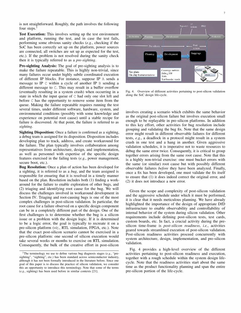
Fig. 4. Overview of different activities pertaining to post-silicon validationalong the SoC design life-cycle.
involves creating a scenario which exhibits the same behavioras the original post-silicon failure but involves execution smallenough to be replayable in pre-silicon platforms. In additionto this key effort, other activities for bug resolution includegrouping and validating the bug fix. Note that the same designerror might result in different observable failures for differenttests, e.g., a deadlock in a protocol might result in a systemcrash in one test and a hang in another. Given aggressivevalidation schedules, it is imperative not to waste resources todebug the same error twice. Consequently, it is critical to grouptogether errors arising from the same root cause. Note that thisis a highly non-trivial exercise: one must bucket errors withthe same (or similar) root cause but with possibly differentobservable failures before they have been analyzed. Finally,once a fix has been developed, one must validate the fix itselfto ensure that (1) it does indeed correct the original error, and(2) it does not introduce a new error.
Given the scope and complexity of post-silicon validationand the aggressive schedule under which it must be performed,it is clear that it needs meticulous planning. We have alreadyhighlighted the importance of the design of appropriate DfDinfrastructure to enable observability and controllability ofinternal behavior of the system during silicon validation. Otherrequirements include defining post-silicon tests, test cards,custom boards, etc. In fact, a crucial activity during the pre-silicon time-frame is post-silicon readiness, i.e., activitiesgeared towards streamlined execution of post-silicon validation.Post-silicon readiness activities proceed concurrently withsystem architecture, design, implementation, and pre-siliconvalidation.
Fig. 4 provides a high-level overview of the differentactivities pertaining to post-silicon readiness and execution,together with a rough schedule within the system design life-cycle. Note that the readiness activities start about the sametime as the product functionality planning and span the entirepre-silicon portion of the life-cycle.

8
A. Test Plans
Test plans constitute arguably the most critical and fun-damental readiness activity for post-silicon validation. Thegoal is to identify the different coverage targets, corner cases,and functionality that need to be tested for the system beingdeployed. Post-silicon test plans are typically more elaboratethan pre-silicon plans, since they often target system-leveluse-cases of the design which cannot be exercised duringpre-silicon validation. Note that test plan development startsconcurrently with design planning. Consequently, when the testplan development starts, a detailed design (or even an elaboratemicroarchitecture for the most part) is unavailable. Initial testplanning correspondingly depends on high-level architecturalspecifications. As the design matures and more and more designfeatures are developed, the test plans undergo refinement toaccount for these features. The plans also need to accountfor the target applications, the new vs. legacy IPs used in thesystem design, etc.
B. On-chip Instrumentation
On-chip instrumentation refers to the DfD features integratedinto the silicon to facilitate post-silicon debug and validation.A key target of the DfD is observability. Modern SoC designsinclude a significant amount of hardware for this purpose, withestimates running to 20% or more in silicon real estate in somecases. Two critical observability features are scan chain [22]and signal tracing [23]. Scan chains enable observability ofthe internal state of the design. Scan chains, of course, arehighly mature architectures originally developed for identifyingmanufacturing defects in the circuit. However, they also providecritical observability during post-silicon validation. Signaltracing, on the other hand, specifically target post-siliconvalidation. The goal is to identify a small set (typically 100s)of internal signals of the design to be observed for each cycleduring silicon execution. To achieve this, the relevant signalsare routed to an observation point, which can be either anoutput pin or a designated section of the memory (referred toas trace buffer). In addition to these two architectures, thereare also instrumentations to transport internal register valuesoff-chip, quickly access large memory arrays, etc. Note thatthese architectures can get highly complex. For example, inrecent SoC designs, data transport mechanisms may re-purposesome of the communication mechanisms already present inthe system, e.g., universal serial bus (USB) port. This requiresa thorough understanding of both the functionality and thevalidation use-cases to ensure that they do not interfere whenusing the same interface. Finally, there is instrumentation toprovide controllability of the execution, e.g., by overriding thesystem configuration, updating microcode on-the-fly duringexecution, etc.
There has recently been significant research on improvingpost-silicon observability through disciplined DfD architecture.Some of the key work in this area has focused on trace signalselection, and we discuss this problem in Section VI. Amongon-chip instrumentation techniques, one of the earliest workis due to Gopalakrishnan and Chou [24]. They use constraintsolving and abstract interpretation to compute state estimates for
memory protocols. Park and Mitra [4] develop an architecturecalled IFRA for disciplined on-chip observability of pipelinedmicroprocessors. Boule et al. [25] present architectures forpost-silicon assertion checkers. Ray and Hunt [7] presentan architecture for on-chip monitor circuits for validation ofspecific concurrent protocols.
C. Debug Software Development
Debug software is another crucial component of post-silicon validation readiness. It includes any software tool andinfrastructure that is necessary to enable running post-silicontests and facilitating debug, triage, or validation of differentcoverage goals. We can categorize debug software roughly intothe following classes.
Instrumented System Software: Post-silicon validation, par-ticularly for hardware logic and compatibility validation,requires running long, complicated tests, identifying complexcorner cases, and root-causing errors excited by subtle hard-ware/software coordination. To achieve this, one typically needsto run an application software stack on the target system.Doing this by executing an application on top of an off-the-shelf operating system is typically difficult. Modern operatingsystems (e.g., Linux, Windows, Android, MacOS, etc.) arehighly optimized for performance and power consumption, andsignificantly complex. To enable debug of underlying hardwareissues one typically needs a highly customized system software,with a reduced set of “bells and whistles” while includinga number of hooks or instrumentations to facilitate debug,observability, and control. For example, one may want to tracethe sequence of branches taken by an application in orderto excite a specific hardware problem. To achieve this, oftenspecialized operating systems are implemented that are targetedfor silicon debug. Such system software may be written bysilicon debug teams from scratch, or by significantly modifyingthe off-the-shelf implementations.
Tracing, Triggers, and Configurations: Some customizedsoftware tools are also developed for controlling, querying,and configuring the internal state of the silicon. In particular,there are tools to query or configure specific hardware registers,setting triggers for tracing, etc. For example, one may wish totrace a specific signal S only when some internal register Rcontains a specific value v. Assuming that both S and R areobservable, one needs software tools to query R and configuresignal tracing to include S when R contains v.
Transport Software: Access software refers to tools thatenable transport of data off-chip from silicon. Data can betransferred off-chip either directly through the pins, or byusing the available ports from the platform (e.g., USB, PCIe,etc.). For example, transporting through the USB port requiresinstrumentation of the USB driver to interpret and route thedebug data while ensuring the USB functionality is not affectedduring normal execution. Note that this can become highlycomplex and subtle, particularly in the presence of other featuresin the SoC such as power management. Power managementmay in fact power down the USB controller when the USBport is not being used by the functional activity of the system.

9
The instrumented driver ensures that debug data is still beingtransported while still facilitating the power-down functionalityof the hardware to be exercised during silicon validation.
Analysis Software: Finally, there are software tools to performanalysis on the transported data. This includes tools to aggregatethe raw signal or trace data into high-level data structures (e.g.,interpreting signal streams from the communication fabric in theSoC as messages or transactions among IPs), comprehendingand visualizing hardware/software coordinations, as well astools to analyze such traced and observed data for furtherhigh-level debug (e.g., to estimate congestion across the com-munication fabric, traffic patterns during internal transactions,power consumption during system execution, etc.).
One critical challenge in developing (and validating) debugsoftware is its tight integration with the target hardware designto be validated. Note that typically software developmentand validation make use of a stable hardware platform,e.g., one develops application software on top of a general-purpose hardware instruction set architecture such as X86 orARM. However, debug software is developed for an under-development target platform often with evolving and changingfeatures (e.g., in response to design or architectural challengesdiscovered late). This makes debug software design a vexingand complex problem in hardware/software co-design and co-validation. Indeed, it is not uncommon in post-silicon validationto root-cause an observed failure to an issue with the debugsoftware rather than the target system. Developing a streamlinedtechnology for debug software development and validation is achallenging area of research.
D. Test Generation and Testing Setup Design
The central component of silicon debug is the set of tests torun. For the validation to be effective, the tests must exposepotential vulnerabilities of the design, and exercise differentcorner cases and configurations. Post-silicon tests can be dividedinto the following two categories.
Focused (Directed) Tests: These are tests carefully crafted byexpert test writers to target specific features of the system (e.g.,multiprocessor and chipset protocols, CPU checks for specificregister configurations, address decoding, power managementfeatures, etc.). Developing such tests involves significant manualeffort. Furthermore, the tests are often extremely long andtargeted, running for several hours on silicon.
Random and Constrained-random Tests: In addition tofocused tests, one exercises system features through randomand constrained-random testing. Examples of such tests includeexecuting a random sequence of system instructions, exercisingconcurrent interleavings, etc. The goal of these tests is toexercise the system in ways not conceived by humans, e.g.,random instruction tests can include 100s of millions of randomseeds generating instruction sequences.
In addition to the tests themselves, their application requiresdevelopment of specialized peripherals, boards, and test cards.This is specifically pertinent for compatibility validation wherethe system needs to be exercised for a large number ofperipheral devices, software versions, and platform features.Section VII describes test generation steps in detail.
E. Towards Standardization of Validation Infrastructure
As evident from the above discussions, post-silicon readinessis a complex and hard problem. To facilitate this, there hasbeen efforts across the industry to standardize the debugand observability architectures. Two such standardizations areARM CoresightTM and Intel R© Platform Analysis Tool. Boththese architectures include a set of hardware IPs (e.g., forcollecting, synchronizing, and time-stamping signal traces andother observability collateral from different design blocks,routing them to output ports and system memory, etc.), andsoftware APIs for configuration, triggering, transport, andanalysis. The specifics of the architectures vary. Coresightarchitecture [26] is instantiated into Macrocells that can interactwith IP functionality through a standard interface. PlatformAnalysis Tool includes a specialized IP called Trace Hub [27]responsible for aggregation and transport of both hardware andsoftware traces, together with APIs that enable direct interactionwith this IP for transport and analysis.
While such standardization assists in streamlining post-siliconreadiness development, it must be emphasized that the currentstate of the art in standardization is rather rudimentary. Forinstance, the software tools to extract trace data for both thearchitectures above are typically APIs for accessing differentinternal design collateral; little assistance is provided to identifythe specific collateral that would be useful or profitable fordebug purposes. It is left to the expertise of the human designerand validator to “hook up” the APIs with the hardware andsoftware content in the target design for achieving validationobjectives.
VI. TRACE SIGNAL SELECTION
In this section, we delve a bit deeper into one aspect ofpost-silicon planning, viz., trace signal selection. As discussedin Section V, trace signals are used to address the observabilitylimitation during post-silicon debug. The basic idea is to tracea set of signals during run time and store in a trace buffer suchthat the traced values can be used during post-silicon debug. It isimportant to note that since I/O speed (using JTAG, for example)is significantly slower than speed of execution (e.g., MHz versusGHz), it is not possible to dump the traced values throughI/O ports during execution. Therefore, internal trace bufferis required. Trace signal selection needs to maintain variousdesign constraints. For example, the trace buffer size directlytranslates to area and power overhead. Moreover, routing theselected signals to the trace buffer may face congestion andother layout related issues. As a result, in a design with millionsof signals, a typical trace buffer traces few hundred signals forfew thousand cycles. For example, a 128× 2048 trace buffercan store 128 signals over 2048 clock cycles. Design overheadconsiderations directly impose two constraints — (i) how toselect a small number of trace signals that can maximize theobservability, and (ii) how to effectively utilize traced valuesfor a small number of cycles to enable meaningful debug.
In post-silicon debug, unknown signal states can be recon-structed from the traced states in two ways - forward andbackward restoration. For example, if one of the inputs of anAND gate is selected as a trace signal and the traced value

10
is ‘0’, we can definitely infer through forward restoration thatthe output of that AND gate should be ‘0’ in that clock cycle.Similarly, if we know the output of an AND gate to be ‘1’ ina specific clock cycle, we can infer using backward restorationthat the inputs of that AND should be all ‘1’s. Of course, inmany scenarios, we need to know values of multiple signals tobe able to restore the values of untraced signals.
Clk
Clk
Clk
Clk
Clk
Clk
Clk
Clk
B
C
D
E
F
H
AG
Fig. 5. An example circuit with 8 flip-flops [28]
One metric used frequently to measure quality of selectedtrace signals is the State Restoration Ratio (SRR), which isbased directly on the idea of reconstructing values of untracedsignals from traced ones. To understand SRR, consider thecircuit shown in Figure 5. The example circuit has 8 flip-flops.Let us assume that the trace buffer width is 2, that is, states oftwo signals can be traced. The approaches of [29] and [30] willselect C and F as trace signals. Table I shows the restoration ofother signals using the traced values of C and F (shaded rowsin the table). For example, if we know C is ‘0’ at clock cycle3, we can infer that both A and B were ‘0’ in the previouscycle (clock cycle 2). Since we know now that A is ‘0’ at clockcycle 2, D should be ‘0’ in the next cycle (clock cycle 3). Thisprocess of forward and backward restoration is continued untilno new values can be restored. The ‘X’s represent those stateswhich cannot be determined. The SRR is then defined as:
RR =# of states restored + # of traced states
number of traced states. (1)
In this example, we have traced 10 states (two signals forfive cycles) and we are able to restore an additional 16 states.Therefore, the restoration ratio is (16 + 10)÷ 10 = 2.6.
TABLE I. RESTORED SIGNALS FROM TRACED ONES ACROSS 5 CYCLES
Signal Cycle 1 Cycle 2 Cycle 3 Cycle 4 Cycle 5
A X 0 X 0 X
B X 0 X 0 X
C 1 1 0 1 0
D X X 0 0 0
E X X 0 0 0
F 0 1 1 0 0
G X 0 0 X 0
H X 0 0 X 0
SRR-based signal selection techniques can be broadly dividedinto three categories. The signal selection techniques in the firstcategory performs structural analysis of the design and selectsthe beneficial signals based on their likelihood in restoringthe unknown (untraced) signals [30], [29], [31], [28]. These
approaches are very fast but they sacrifice the restorability.On the other hand, the simulation based signal selectiontechniques [32] utilize the deterministic nature of the signals inidentifying the most profitable trace signals. This approachprovides superior restoration quality but incurs prohibitivecomputation overhead. The third category of techniques triesto combine the advantages of both approaches utilizing hybrid[33], ILP [34] and machine learning [35], [36] techniques.There are also various approaches that try to take advantage ofboth trace and scan signals to improve post-silicon observability[37], [38].
We should point out that while SRR is widely used todayas a research vehicle in evaluating trace signal quality, weare not aware of any industrial report on application of SRR.This is due to a variety of reasons. For instance, SRR doesnot account for design functionality in signal evaluation. Notethat the same IP may be used in different use cases, and thevalidation requirement (and consequently, the correspondingobservability) depends on the deployment target. Furthermore,SRR does not account for architectural and physical constraintsthat may preclude some signals from being selected, nor doesit account for the fact that there is a significant amount of otherDfD components that may be used in conjunction with tracingto facilitate observability.
To address the above challenges with SRR, other approacheshave been proposed. In particular, there are approaches involv-ing insertion of faults in the design and identifying signals bestfor identifying such faults [39]. Other approaches take a morefunctional view of the design, and attempt to identify signalsbest for a specific functionality. For example, in recent work, aversion of the Google Pagerank algorithm was used for signalselection and showed a more promising coverage of designassertions [40]. Nevertheless, much research remains to be doneto make signal selection more disciplined and systematic.
VII. TEST GENERATION
Post-silicon validation is one stage of the complete verifica-tion cycle which starts with pre-silicon verification. However,both pre- and post-silicon verification cannot achieve theirgoals on their own; pre-silicon, in terms of finding all thebugs before tape-out, and post-silicon, in terms of findingthe bugs that escaped pre-silicon. This creates an increasingneed to bridge the gap between these two domains by sharingmethodologies and technologies and building a bridge allowingeasier integration between the domains. The need for strongconnection between pre- and post-silicon is particularly evidentin test generation, where post-silicon tests must be generatedby making use of pre-silicon collateral and the generationprocedure often span across the two phases.
A. Pre-silicon Stimuli Generation
A pre-silicon stimuli generator has to provide the user withthe ability to specify the desired scenarios in some convenientway, and produce many valid high-quality test-cases accordingto the user’s specification. These scenario specifications - termedtest templates - are written in a language that should enablean easy and accurate way for specifying the scenarios from

11
Fig. 7. Threadmill Vs. Genesys-Pro tool flows
the verification plan. Figure 6 shows an example of a testtemplate that defines a table-walk scenario (on the left) and anexample of a test generated from this template (on the right).The test template is written in the test template language ofGenesys-Pro [41] - IBM’s well established test generation toolfor the functional verification of processors using a softwaresimulator platform. The rest of this section describes Genesys-Pro’s approach to test generation.
The scenario of Figure 6 starts with a Store and then asequence of Loads each followed by a either an Add or aSub instruction. The memory locations accessed by the Loadinstructions are contiguous in memory as seen in the ResourceInitial Values section of the test (addresses 0x100–0x1F0). Thisis managed by a test-template variable addr.
The use of test-templates thus separates the test-templatewriting activity from the generator’s development activity.The language consists of four types of statements: basicinstruction statements, sequencing-control statements, standardprogramming constructs, and constraint statements. Userscombine these statements to compose complex test-templatesthat capture the essence of the targeted scenarios, leaving outunnecessary details. This allows directing the generator to aspecific area, be it a small or a large one.
The generated test-cases must be valid according to theprocessor’s architecture, and satisfy the user’s request specifiedin the template. In addition, they should also be different fromeach other as much as possible. This is done by specifyingthe rules determining the validity of a test-case, as well asthe user requests as constraints. The generator, then, producesa test-case by random sampling of the solution space to theresulting constraints satisfaction problem [42].
The distribution of the generated tests should not be uniform,as verification engineers would like to favor tests that include in-teresting verification events (e.g., register dependency, memorycollisions), especially ones that are extremely unlikely to occurunder uniform distribution. This is done by having knowledgeembedded in the generator, allowing it to bias random decisions
Fig. 8. A unified verification methodology
towards stimuli that causes interesting events [42]. This testingknowledge defines the interesting verification events, includingthe stimuli that trigger them. As the stimuli for some interestingevents depend on the processor’s state, the generator alsoemploys a reference model of the DUV, simulating on it forevery generated instruction. This way the generator maintainsan accurate view of all the architectural resources, taking it intoaccount during generation of interesting events. This schemeis shown in the lower part of Figure 7.
Genesys-Pro has been in use by IBM for over fifteen years.It has proven to be effective in meeting the users requirements,enabling them to write test-templates implementing the coreverification plans of IBM’s complex processors [43].
B. A Unified Verification Methodology
To better integrate post-silicon validation to the overallverification process and improve its synergy with pre-siliconverification, a unified verification methodology is needed thatis fed from the same verification plan source. A key ingredientfor the success of such methodology is providing commonlanguages for the pre- and post-silicon aspects of it in terms oftest specification, progress measure, etc. Figure 8 depicts sucha methodology. This verification methodology leverages threedifferent platforms: simulation, acceleration, and silicon. Themethodology requires three major components: a verificationplan, directable stimuli generators suited to each platform, andfunctional coverage models. Note that important aspects in anyverification methodology, such as checking, are omitted fromthe figure to maintain focus on stimuli generation.
The verification plan includes a long list of line-items, eachtargeting a feature in the DUV that needs to be verified.Each such feature is associated with coverage events that theverification team expects to observe during the verificationprocess and the methods to be used to verify the feature.The verification plan is implemented using random stimuligenerators that produce a large number of test-cases, andcoverage tools that look for the occurrence of events in theverification plan. The random stimuli generators are directedtowards the verification goals by using test-templates. The test-templates allow the generators to focus on areas in the DUVranging from large generic areas, like the floating-point unit, tovery specific areas, like a bypass between stages of the pipeline.Coverage analysis identifies gaps in the implementation of the

12
Test Program Template Test Program
Variable: addr = 0x100 Resource Initial Values:Variable: reg R6=8, R3=-25,..., R17=-16
Bias: register-dependency 100=7, 110=25,..., 1F0=16
Instructions:Instruction: Store R5 → ? 500: Store R5 → FF0
Repeat (addr < 0x200) 504: Load R4 ← 100
Instruction: Load reg ← addr 508: Sub R5 ← R6-R4
Select 50C: Load R4 ← 110
Instruction: Add ? ← reg + ? 510: Add R6 ← R4+R3
Bias: sum-zero :Instruction: Sub ? ← ? - ? 57C: Load R4 ← 1F0
addr = addr + 0x10 580: Add R9 ← R4+R17
Fig. 6. Test template and corresponding test
plan. Its feedback is used to modify test-templates that do notfulfill their goals, and create new ones.
This methodology is extended to post-silicon validation byleveraging the acceleration platform to measure coverage ofpost-silicon tools. To take advantage of the coverage informationcollected by the accelerators and use it in the post-silicon,shortly before first silicon samples come back from the fab,a regression suite of exerciser test-templates is created basedon the coverage achieved on the accelerators. This regressionsuite is then used to continue the verification process on thesilicon platform.
With the unified methodology, each of the line-items in theverification plan is attached to one or more target platformson which it will be verified. These line-items are converted totest-templates in the languages of the generation tools used byeach platform. A key ingredient for the success of the unifiedmethodology is similar operation of the stimuli generators. Inthis sense, designers would like the generators to use the sametest-template language, and when provided with the same test-template, one would like the tools to produce similar (thoughnot identical) test-cases. Of course, the different platformsprovide different opportunities and put different constraints andrequirements on the generation tools, but whenever possible,there are advantages to having similar tools. First, the pre- andpost-silicon teams can share the task of understanding the line-items in the verification plan and planning ways to test them.In addition, the common language allows for easier adaptationof test-templates from one platform to another. For example,when a bug is detected on the silicon platform, narrowing downthe test-template and hitting it on the simulation platform easesthe root-cause analysis effort.
It is important to note that the differences between platformsalso dictate differences in the way test-templates are writtenfor pre- and post-silicon tools. A test-template could be veryspecific and describe a small set of targeted tests or it couldbe more general leaving more room for randomization. Thevalidation engineer writing test-templates for a post-siliconexerciser must bear in mind the fact that the test-template isused to generate a huge number of test-cases and get manyprocessor cycles. To effectively use these test cycles, the test-template must allow for enough interesting variation. A testtemplate that is too specific will quickly “run out of steam”
on silicon and start repeating similar tests. A pre-silicon testtemplate on the other hand would typically be more directed toensure that the targeted scenarios are reached within the fewercycles available on simulation. There are also many efforts inautomated generation of directed tests using formal methods[44], [45], [46], [47], [48].
C. Threadmill
Threadmill was developed in IBM for the purpose of enablingthe unified methodology described in the previous sub-section;namely, to support a verification process guided by a verificationplan by enabling the validation engineers to guide the exerciserthrough test-templates. The high-level tool architecture ofThreadmill is depicted in Figure 7, along with the flow ofGenesys-Pro [49] - the pre-silicon test generator tool describedin sub-section VII-A.
Like Genesys-Pro, the main input to Threadmill is a test-template that specifies the desired scenarios. As describedearlier, the templates used for pre- and post-silicon testshave different characteristics. The test-template language ofThreadmill is very similar to the language of Genesys-Pro butto adhere to the simplicity and generation speed requirements,several constructs that require long generation time, such asevents, are not included in Threadmill’s language. Other inputsto Threadmill are the architectural model and testing knowledgeand the system topology. Again, for simplicity reasons, manytesting knowledge items that are included in Genesys-Promodels are not used by Threadmill.
The Threadmill execution process starts with a builderapplication that runs off-line to create an executable exerciserimage. The role of the builder is to convert the data incorporatedin the test-template and the architectural model into datastructures that are then embedded into the exerciser image.This scheme eliminates the need to access files or databaseswhile the exerciser is running.
The exerciser image is composed of three major components:a thin, OS-like, layer of basic services required for Threadmill’sbare-metal execution; a representation of the test-template,architectural model and system configuration description assimple data structures; and fixed (test-template independent)code that is responsible for exercising. The executable imagecreated by the builder is then loaded onto the silicon platform

13
where the exerciser indefinitely repeats the process of generatinga random test-case based on the test-template, the configurationand the architectural model, executing it, and checking itsresults.
In case of Genesys-Pro, the test generation process is carriedoutside of the simulation environment (say on a dedicatedserver) and only the generated tests are loaded and run on thesimulation platform. Simulation cycles would be too slow toallow generation on simulation. The “off-line” generation on theother hand can afford to spend time on sophisticated generationand checking - for example by using a reference-model asshown in Figure 7 for Genesys-Pro. Threadmill’s test generationcomponent was designed to be simple and fast. Therefore, IBMdesigners opted for a static test generator that does not make useof a reference model. Reference models provide the generatorinformation about the state of the processor before and afterthe generation of each instruction. This information is used forchecking but also to create more interesting events. Reloadingresources, such as registers, can be a partial replacement to thereference model, but this solution potentially interferes withthe generation of the requested scenarios. For data-orientedevents, such as divide-by-zero, a simple yet effective solutionis to reserve registers to hold interesting values. Of course,the generator has to ensure that the reserved registers are notmodified during the test.
Execution of the same test-case multiple times is used as apartial replacement for checking done by the reference model.This is done by comparison of certain resource values such asregisters and part of the memory for consistency in differentexecutions of the test-case. Running the same test-case multipletimes may result in different results even when bugs are notpresent. For example, when several threads write to the samememory location, the final value at this location depends onthe order of the write operations. This requires that certainmechanisms be implemented in the generator to restrict thenumber of unpredictable resources. Although the multi-passcomparison checking technique is limited, it has proven to beeffective when control-path oriented bugs, or bugs that reside inthe intersection of the control- and data-paths, are concerned. Toincrease the probability of exposing such bugs, it is beneficialto introduce some kind of variability into the different executionpasses, while making sure that the variability maintains thepredictability of the compared resources. This can be done, forexample, by changing the machine mode, or changing threadpriorities.
D. Tests Targeting Errors
We now turn to the question: how can we ensure that a testexcites a bug and propagates it to a failure within a reasonabletime? In this subsection we consider the question from theperspective of test generation; in the next subsection the samequestion will be considered from the perspective of observabilityconstraints.
Traditionally, post-silicon tests have sported a long latencybetween when a bug is excited and when its effect is observedas a failure. For instance, consider a memory write to someaddress that writes an incorrect value. The effect of this bug
may not be observed unless the value written is subsequentlyread (maybe several thousands of cycles later) and the errorresulting from this read propagated to cause some observableeffects. Clearly, it is important to reduce the latency of errorobservability, from the point in which the bug is triggered toan observable effect.
There has been significant research in developing effectivepost-silicon tests. In particular, a general technique called“Quick Error Detection” (QED) specifically focuses on reducingthe latency mentioned above [50], [51]. The idea is to transforma test into another one with lower latency between bugexcitation and failure. For instance, for the memory readexample above, a QED test would transform the original testby introducing a memory read immediately after each memorywrite; thus, an error introduced by the write would be excitedimmediately by the corresponding read. Note that doing thisin general requires a comprehensive characterization of errorsin terms of a cause-effect relationship. QED manages it bydefining this relationship for errors in a number of categories. Bycapturing a diversity of error characterizations, it has managedto be successfully adapted for a diversity of post-silicon tests,including those for functional as well as electrical errors.
E. Observability-aware Test Generation
Observability constraints make it difficult to diagnose bugs.In fact, it is also difficult to figure out if a test has executed asexpected, if the result of that test execution activates a signalwhich is not observable. Therefore, it is crucial that the post-silicon tests are observable directly (if it activates one of thetrace signals) or indirectly (values of the activated signal canbe restored using the trace signals). Unfortunately, it would behard to generate observability-aware tests for various reasons.First, the post-silicon test generation and trace signal selectionare typically performed concurrently by different teams duringan industrial SoC development. Moreover, it is difficult toperform automated generation of observability-aware directedtests after the observability architecture has been defined. Thisis due to the fact that such a test generation approach wouldrequire analysis of complex and potentially buggy RTL models.Industrial RTL models consist of millions of lines of code, andtherefore, automated formal analysis of such models exceedsthe capacity limitations of directed test generation tools. Even ifsuch an analysis was possible, the generated test would not beuseful if the RTL models contains functional or design errors- an erroneous model can at best lead to generation of buggytests, which is unlikely to activate the design flaws. Even if itactivates a specific scenario, the accuracy of such a validationmethod becomes questionable.
Recent research efforts [52] provide an alternative mecha-nism to generate observability-aware post-silicon tests usinggolden pre-silicon models. The test generation is performed byanalyzing golden transaction-level models (TLM) instead ofbuggy RTL models. Analysis of TLM model also takes careof scalability issue since a TLM model is significantly simplerthan the respective RTL model. Clearly, this approach requiresa golden TLM model. This work also assumes that both TLMand RTL models have the same input/output interfaces at both

14
Fig. 9. Observability-aware test generation consists of four important steps:construct RTL assertion with observability constraints, map RTL assertion toTLM, generate TLM test, translate TLM to RTL test
SoC and individual component levels. This is reasonable forSoC design since it consists of hardware or software intellectualproperty (IP) blocks with well-defined interfaces.
Figure 9 provides an overview of observability-aware testgeneration for a given RTL assertion. This approach involvesfour important steps: i) defining test targets with observabilityconstraints, ii) mapping test targets from RTL to TLM, iii) testgeneration using TLM model, and iv) translating TLM teststo RTL tests. This work essentially incorporates observabilityconstraints into an RTL assertion to create a new RTL assertion.The modified assertion is then mapped to a TLM property. TheTLM property is used to automatically construct a TLM test.The last step is to convert the generated TLM test to an RTLtest [53]. The generated RTL test is observability-friendly sinceit would not only activate the assertion, but also propagate itseffects to the observability architecture (e.g., trace signals).
VIII. POST-SILICON VALIDATION OF IBM POWER8
In this section, we provide a high-level overview of the post-silicon methodology and technologies put into use for functionalvalidation of POWER8. We describe various factors thatcontributed to this successful bring-up. A detailed discussionon the functional verification of POWER8 and its bring-up canbe found in [54], [55].
A. The POWER8 Chip
POWER8 is the latest IBM chip in the POWER series.Designed for high-end enterprise-class servers, it is one ofthe most complex processors ever created. The POWER8 chipis fabricated with IBM’s 22nm silicon-on-insulator technologyusing copper interconnects and 15 layers of metal. The chip is650mm2 and contains over 5 billion transistors.
Figure 10 depicts a high-level block diagram of the POWER8processor chip. Each processor chip has 12 cores. Each core is
Fig. 10. The POWER8 Processor Chip
capable of 8-way simultaneous-multithreading (SMT) operation,and can issue up to 10 instructions every cycle. The memoryhierarchy includes a per-core L1 cache, a per-core SRAM-based512KB L2 cache, and an eDRAM based shared L3 cache. Inaddition, an off-chip eDRAM L4 cache per memory bufferchip is supported. There are 2 memory controllers on the chipsupporting a sustained bandwidth of up to 230GB per second.The chip also holds a set of hardware accelerators, including acryptographic accelerator and a memory compress/decompressmechanism. Finally, the chip includes a PCIe adapter and bridgeto a bus supporting a coherent connection to an FPGA. TheFPGA is directly accessible to user applications through ahashed table translation.
B. Preparing for the Lab
The bring-up work of POWER8 started way before siliconsamples were ready. The team responsible for preparing thetools and tests for the lab began its work as soon as the keyfeatures of POWER8 were determined at the High Level Design(HLD) stage. The first step in that work was to ensure that thepost-silicon tool teams better understand the new features theyneed to support and the design team understand the validationrequirements and incorporate them into the design.
When sufficient functional stability was achieved, the pre-silicon verification team, together with the exerciser team,started running exerciser shifts on Awan simulation accelerationplatform [56]. This phase, termed Exercisers on Accelerator(EoA), achieved several goals. First, it ensured the qualityof the exercisers software. In addition, it helped the pre-silicon verification of POWER8. In fact, EoA was responsiblefor finding about 1% of the total bugs found in pre-siliconverification. Finally, EoA was used to develop and test theshifts that were later used during the actual bring-up.
To that extent, an important aspect of the EoA work wasthe synthesis of coverage monitors synthesized into the DUTmodel. These coverage monitors were added to the logic

15
model running on the accelerator, but not to the siliconitself, because of area, timing, and power issues. Leveragingacceleration-synthesized coverage monitors allowed the useof a pre-silicon-like coverage-driven methodology for post-silicon test-development [57]. With this approach, the exercisershift developers could validate that a specific shift covers thetargeted functionality. This is done by observing that the relatedcoverage events are hit when the exerciser shift is run on theaccelerator. The acceleration-synthesized coverage monitorsplayed a major role in selecting which shifts to run duringbring-up to best utilize the scarce silicon resources. There arealso recent efforts in post-silicon coverage analysis withoutusing synthesized coverage monitors [58]. A different use ofaccelerators during the bring-up preparation was to prepare thedifferent procedures and tools for the lab team. This includedthe validation of the different steps required to boot the system(Virtual Power-On, or VPO), track the execution of an exerciseras it runs, and dump and format debug data from the embeddedtrace arrays.
C. Triggering Bus — Stimuli Generation
Bare-metal exercisers (an example of which is described inSection VII-C) were the primary vehicle for test-case generationin the POWER8 post-silicon validation. The characteristics ofthe post-silicon platforms create challenges and impose trade-offs that affect the design of these exercisers. While post-siliconplatforms offer a huge number of execution cycles, their lowavailability and high cost calls for maximizing the time spentexecuting test-cases and minimizing overhead. Accordingly, theexerciser team developed a set of exercisers, each capturing adifferent trade-off between generation complexity and checkingcapabilities. Bare-metal exercisers possess a list of attributesthat make them highly suitable for post-silicon validation. Bare-metal exercisers are inherently “self-contained”, meaning thatonce the exerciser shift is loaded onto the platform, be itan accelerator or a silicon one, it can run “forever” with nointeraction with the environment. This significantly reducesthe overhead related to initializing the platform, loading theexerciser, and so on.
Overall, during the POWER8 pre-and post-silicon develop-ment process, the bare-metal exercisers approach proved highlysuccessful, as in the case of other previous processors. Thisapproach is key in IBM’s post-silicon validation strategy. In fact,bugs that were found with OS-based tests or actual softwareare considered escapes from our validation strategy.
In addition to bare-metal exercisers, IBM designers leverageda set of hardware irritators embedded in the design. A hardwareirritator is a piece of logic embedded in the design that cantrigger microarchitectural events at random. The irritatorsare initialized during the processor’s power-on sequence, andrandomly inject events as the processor executes instructions.For example, an irritator can be used to flush the pipeline atrandom, without having the executed instruction stream createthe conditions required for this event.
Irritators are extremely useful in bringing the DUT to some“tough” corners, without creating the stimuli needed to actuallyreach these corners. Furthermore, irritators can mimic large
system behavior. For example, in a single chip system, anirritator can inject a random Translation Lookaside Buffer (TLB)invalidate-entry event as if it were coming from a differentchip.
Different components in the POWER8 chip support nonfunc-tional running modes, introduced for the sake of validation.These modes further assisted the bring-up team in stressingthe design. For example, the POWER8 L2 cache supports amode in which almost every access would trigger a cast-out.By setting the processor to this state, one could aggravate thestress on the L3 cache.
Since hardware irritators and non-functional modes areembedded in the design, and, accordingly, have an overheadin terms of area and power, they must be carefully thought ofand designed as part of the processor.
D. Checking
POWER8 employed two main checking techniques in itspost-silicon validation: checkers embedded in the hardware andsoftware checkers that are part of the bare-metal exercisers.Hardware-based checkers were designed and embedded intothe POWER8 processor. These checkers cover some genericerroneous behavior such as access out of memory, and a timer-based hang checkers for instruction completion.
During the POWER8 post-silicon validation, it was easierto debug failures triggered by hardware-based checkers. Thiswas because when a failure was triggered by such a checker,the DUT was stopped fairly close to the origin of the bug.Accordingly, the debug logic, once configured to trace therelevant component in the design, typically contained valuablehints as to the origin of the bug. Furthermore, some checkersprovide an initial indication when they fire. For example, whenthe access out of memory checker fires, the transaction thattriggered it is captured in the bus’ debug logic and points tothe hardware thread and address that triggered the fail.
Despite their effectiveness, the use of hardware-based check-ers is limited due to their high cost in terms of area and power,and their effect on timing. Therefore, software-based checkerswere also heavily used for failure detection in the POWER8post-silicon validation.
Bare-metal exercisers employ a checking technique calledmulti-pass consistency checking [59]. In this technique, everytest-case is executed several times (passes). The first passis referred to as a reference pass, and the values of certainresources, such as architected registers and some memory, aresaved at the end of the execution of this pass. After followingpasses, the exerciser compares the end-of-pass values withthose of the reference pass. In case an inconsistency is detected,the error is reported and the execution is stopped. The multi-pass consistency checking technique imposes restrictions ontest-generation. For example, write-write collisions betweendifferent threads to the same memory location, where the orderof thread accesses cannot be determined may yield inconsistentresults and are therefore not supported.
Multi-pass consistency failures were very hard to debug. Thisoccurred primarily because the checking flags the error millions,and sometimes billions, of cycles after the error first occurred.
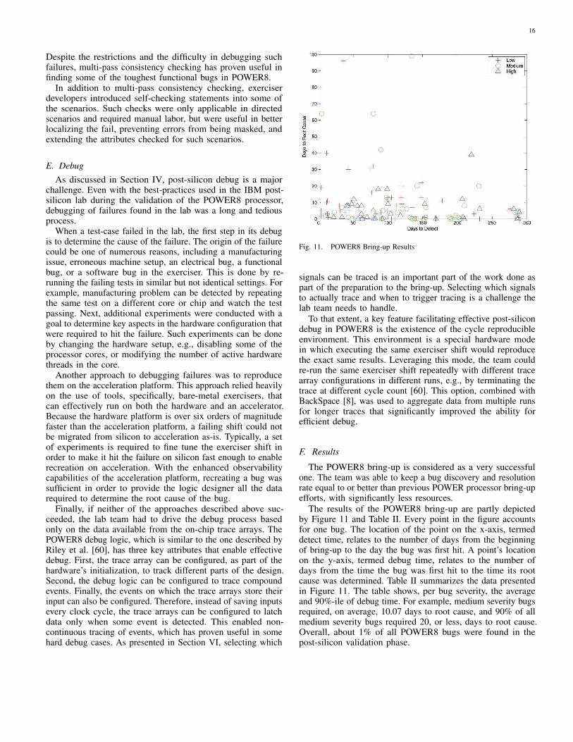
16
Despite the restrictions and the difficulty in debugging suchfailures, multi-pass consistency checking has proven useful infinding some of the toughest functional bugs in POWER8.
In addition to multi-pass consistency checking, exerciserdevelopers introduced self-checking statements into some ofthe scenarios. Such checks were only applicable in directedscenarios and required manual labor, but were useful in betterlocalizing the fail, preventing errors from being masked, andextending the attributes checked for such scenarios.
E. Debug
As discussed in Section IV, post-silicon debug is a majorchallenge. Even with the best-practices used in the IBM post-silicon lab during the validation of the POWER8 processor,debugging of failures found in the lab was a long and tediousprocess.
When a test-case failed in the lab, the first step in its debugis to determine the cause of the failure. The origin of the failurecould be one of numerous reasons, including a manufacturingissue, erroneous machine setup, an electrical bug, a functionalbug, or a software bug in the exerciser. This is done by re-running the failing tests in similar but not identical settings. Forexample, manufacturing problem can be detected by repeatingthe same test on a different core or chip and watch the testpassing. Next, additional experiments were conducted with agoal to determine key aspects in the hardware configuration thatwere required to hit the failure. Such experiments can be doneby changing the hardware setup, e.g., disabling some of theprocessor cores, or modifying the number of active hardwarethreads in the core.
Another approach to debugging failures was to reproducethem on the acceleration platform. This approach relied heavilyon the use of tools, specifically, bare-metal exercisers, thatcan effectively run on both the hardware and an accelerator.Because the hardware platform is over six orders of magnitudefaster than the acceleration platform, a failing shift could notbe migrated from silicon to acceleration as-is. Typically, a setof experiments is required to fine tune the exerciser shift inorder to make it hit the failure on silicon fast enough to enablerecreation on acceleration. With the enhanced observabilitycapabilities of the acceleration platform, recreating a bug wassufficient in order to provide the logic designer all the datarequired to determine the root cause of the bug.
Finally, if neither of the approaches described above suc-ceeded, the lab team had to drive the debug process basedonly on the data available from the on-chip trace arrays. ThePOWER8 debug logic, which is similar to the one described byRiley et al. [60], has three key attributes that enable effectivedebug. First, the trace array can be configured, as part of thehardware’s initialization, to track different parts of the design.Second, the debug logic can be configured to trace compoundevents. Finally, the events on which the trace arrays store theirinput can also be configured. Therefore, instead of saving inputsevery clock cycle, the trace arrays can be configured to latchdata only when some event is detected. This enabled non-continuous tracing of events, which has proven useful in somehard debug cases. As presented in Section VI, selecting which
Fig. 11. POWER8 Bring-up Results
signals can be traced is an important part of the work done aspart of the preparation to the bring-up. Selecting which signalsto actually trace and when to trigger tracing is a challenge thelab team needs to handle.
To that extent, a key feature facilitating effective post-silicondebug in POWER8 is the existence of the cycle reproducibleenvironment. This environment is a special hardware modein which executing the same exerciser shift would reproducethe exact same results. Leveraging this mode, the team couldre-run the same exerciser shift repeatedly with different tracearray configurations in different runs, e.g., by terminating thetrace at different cycle count [60]. This option, combined withBackSpace [8], was used to aggregate data from multiple runsfor longer traces that significantly improved the ability forefficient debug.
F. Results
The POWER8 bring-up is considered as a very successfulone. The team was able to keep a bug discovery and resolutionrate equal to or better than previous POWER processor bring-upefforts, with significantly less resources.
The results of the POWER8 bring-up are partly depictedby Figure 11 and Table II. Every point in the figure accountsfor one bug. The location of the point on the x-axis, termeddetect time, relates to the number of days from the beginningof bring-up to the day the bug was first hit. A point’s locationon the y-axis, termed debug time, relates to the number ofdays from the time the bug was first hit to the time its rootcause was determined. Table II summarizes the data presentedin Figure 11. The table shows, per bug severity, the averageand 90%-ile of debug time. For example, medium severity bugsrequired, on average, 10.07 days to root cause, and 90% of allmedium severity bugs required 20, or less, days to root cause.Overall, about 1% of all POWER8 bugs were found in thepost-silicon validation phase.

17
Average 90%
Low 9.92 22
Medium 10.07 20
High 5.96 12
TABLE II. STATISTICS OF DAYS TO ROOT CAUSE
The bugs are divided into three classes, based on their severity.The severity of the bug was determined based on a combinationof the impact of the bug on the functional behavior of thesystem, the performance cost of working around the bug (ifthat was possible) and the complexity of the fix. The severityof a bug could only be determined after its root cause wasfound and a fix was suggested. Figure 11 shows that the debugtime for high severity bugs is significantly lower, on average,than that of other classes of bugs. This indicates that the labteam effectively speculated the severity of each bug at a veryearly stage. This is attributed to the expertise of the lab teammembers; based on the limited data available, they were ableto infer the real nature of the bug and its expected severitywhen the bug was first detected.
Figure 11 also shows how the rigorous preparations forthe bring-up paid off. Half of all POWER8 post-silicon bugswere found in the first three months of the bring-up. Thisis considered very good result, since during the first twomonths of the bring-up the team had to dedicate a lot oftime to overcoming hardware stability issues and to “screen”the manufactured chips for good functioning ones.
IX. CONCLUSION
We have provided an overview of post-silicon validation anddebug for heterogeneous SoCs. We have described variouschallenges in performing post-silicon validation. We alsosurveyed existing approaches to address these challenges. Theimportance of post-silicon validation has increased steadily overthe years — many studies suggest up to 50% overall cost (time)for post-silicon validation. Considering the dramatic increasein the number of IoT devices in a wide variety of domains,post-silicon validation of SoC designs is expected to remainin the limelight for a long time. Although this paper covereda wide variety of topics related to post-silicon validation anddebug, the materials discussed here form only the tip of theiceberg of this large and exciting domain. Nevertheless, wehope this paper provides a starting point for researchers inunderstanding the industrial practice and research challenges inthis area. There is a significant scope for pushing the researchenvelope above and beyond current limits, and it is crucial thatwe do so to enable development of cost-effective, reliable, andsecure computing systems.
ACKNOWLEDGMENTS
This work was partially supported by the NSF grants(CCF-1218629 and CNS-1441667) and SRC grant (2014-TS-2554). Any opinions, findings, conclusions or recommendationspresented in this article are only those of the authors; and do notnecessarily reflect the views of the National Science Foundationor Semiconductor Research Corporation.
REFERENCES
[1] S. Ray, Y. Jin, and A. Raychowdhury, “The Changing ComputingParadigm with Internet of Things: A Tutorial Introduction,” IEEE Design
& Test of Computers, vol. 33, no. 2, pp. 76–96, 2016.
[2] D. Evans, “The internet of things - how the next evolution of the internetis changing everything,” White Paper. Cisco Internet Business Solutions
Group (IBSG), 2011.
[3] Prabhat Mishra and Nikil Dutt, Functional Verification of Programmable
Embedded Architectures: A Top-Down Approach. Springer, 2005.
[4] Sung-Boem Park, T. Hong and Subhasish Mitra, “Post-silicon buglocalization in processors using instruction footprint recording andanalysis (ifra),” IEEE Transactions on Computer-Aided Design of
Integrated Circuits and Systems (TCAD), vol. 28, no. 10, pp. 1545–1558, 2009.
[5] V. V. Ethiraj and K. Safford, “PSMI Using At-Speed Scan Capture,”2011, U.S. Patent App. PCT/US2011/066-656.
[6] R. Rodrigues and S. Kundu, “Shadow Checker: A Low-Cost HardwareScheme for Online Detection of Faults in Small Memory Structures ofa Microprocessor,” in ITC, 2010.
[7] S. Ray and W. A. Hunt, Jr., “Connecting Pre-Silicon and Post-siliconVerification,” in Proceedings of the 9th International Conference on
Formal Methods in Computer-Aided Design (FMCAD 2009), A. Biereand C. Pixley, Eds. Austin, TX: IEEE Computer Society, Nov. 2009,pp. 160–163.
[8] F. M. De Paula, A. J. Hu, and A. Nahir, “nuTAB-BackSpace: rewriting tonormalize non-determinism in post-silicon debug traces,” in International
Conference on Computer Aided Verification, 2012, pp. 513–531.
[9] Virutech Simics, http://www.simics.net, 2009.
[10] “Prototyping with Virtualizer,” See URL http://www.synop-sys.com/Prototyping/VirtualPrototyping/Pages/virtualizer.aspx.
[11] “Zebu,” See URL http://www.synopsys.com/tools/verification/hardware-verification/emulation/Pages/default.aspx.
[12] “Palladium Z1 Enterprise Emulation System,” See URLwww.cadence.com.
[13] “Veloce2 Emulator,” See URL https://www.mentor.com-/products/fv/emulation-systems/veloce.
[14] R. Rowlette and T. Elies, “Critical Timing Analysis in MicroprocessorsUsing Near-IR Laser-Assisted Device Alteration (LADA),” in Interna-
tional Test Conference, 2003, pp. 264–273.
[15] S. Ram, S. Rusu, U. N. Desai, R. Kim, J. Zhang, and I. Young, “ClockGeneration and Distribution for the First IA-64 Microprocessor,” IEEE
Journal of Solid State Circuits, vol. 35, pp. 1545–1552, 2000.
[16] D. Kaiss and J. Kalechstain, “Post-silicon Timing Diagnosis MadeSimple Using Formal Technology,” in FMCAD, 2014, pp. 131–138.
[17] O. Olivo, S. Ray, J. Bhadra, and V. Vedula, “A Unified Formal Frameworkfor Analyzing Functional and Speed-path Properties,” in Microprocessor
Test and Verification, 2011, pp. 44–45.
[18] X. Guo, R. Dutta, Y. Jin, F. Farahmandi and P. Mishra, “Pre-siliconsecurity verification and validation: A formal perspective,” in Proceedings
of Design Automation Conference (DAC), 2015.
[19] Homebrew Development Wiki, “JTAG-Hack,”http://dev360.wikia.com/wiki/JTAG-Hack.
[20] L. Greenemeier, “iPhone Hacks Annoy AT&T but Are Unlikely toBruise Apple,” Scientific American, 2007.
[21] E. Seligman, T. Schubert, and M. V. A. Kiran Kumar, Formal Verification:
An Essential Toolkit for Modern VLSI Design. Morgan Kaufman, 2015.
[22] M. Abramovici, P. Bradley, K. Dwarkanath, P. Levin, G. Memi, andD. Miller, “A Reconfigurable Design-for-Debug Infrastructure for SoCs,”in Proceedings of the 43rd Design Automation Conference (DAC 2006).ACM/IEEE, 2006, pp. 7–12.
[23] P. Patra, “On the cusp of a validation wall,” IEEE Design & Test of
Computer, vol. 24, no. 2, pp. 193–196, Mar. 2007.

18
[24] G. Gopalakrishnan and C. Chou, “The Post-silicon Verification Problem:Designing Limited Observability Checkers for Shared Memory Proces-sors,” in 5th International Workshop on Designing Correct Circuits
(DCC 2004), M. Sheeran and T. Melham, Eds., Mar. 2004.
[25] M. Boule, J. Chenard, and Z. Zilic, “Adding Debug Enhancements toAssertion Checkers for Hardware Emulation and Silicon Debug,” inInternational Conference on Computer Design. IEEE Computer Society,2006, pp. 294–299.
[26] “CoreSight On-chip Trace & Debug Architecture, www.arm.com.”
[27] “Intel R© Platform Analysis Library,” https://software.intel.com/en-us/intel-platform-analysis-library.
[28] K. Basu and P. Mishra, “Restoration-aware trace signal selection for postsilicon validation,” IEEE Transactions on Very Large Scale Integration
Systems (TVLSI), vol. 21, no. 4, pp. 605–613, 2013.
[29] H. F. Ko and N. Nicolici, “Algorithms for state restoration and trace-signal selection for data acquisition in silicon debug,” IEEE Transactions
on Computer-Aided Design of Integrated Circuits and Systems, vol. 28,no. 2, pp. 285–297, Feb. 2009.
[30] X. Liu and Q. Xu, “Trace signal selection for visibility enhancement inpost-silicon validation,” in Proceedings of the Design Automation and
Test in Europe, 2009.
[31] S. Prabhakar and M. Hsiao, “Using non-trivial logic implications fortrace buffer-based silicon debug,” in Proc. of Asian Test Symposium
(ATS), 2009, pp. 131–136.
[32] D. Chatterjee, C. McCarter, and V. Bertacco, “Simulation-based signalselection for state restoration in silicon debug,” in Proceedings of
International Conference on Computer-Aided Design (ICCAD), 2011,pp. 595–601.
[33] M. Li and A. Davoodi, “A hybrid approach for fast and accurate tracesignal selection for post-silicon debug,” in Design Automation and Test
in Europe (DATE), 2013, pp. 485–490.
[34] K. Rahmani, P. Mishra and S. Ray, “Efficient trace signal selectionusing augmentation and ILP techniques,” in International Symposium
on Quality Electronic Design (ISQED), 2014, pp. 148–155.
[35] ——, “Scalable trace signal selection using machine learning,” in IEEE
International Conference on Computer Design (ICCD), 2013, pp. 384–389.
[36] K. Rahmani, S. Ray and P. Mishra, “Post-silicon trace signal selectionusing machine learning techniques,” IEEE Transactions on Very Large
Scale Integration Systems (TVLSI), 2017.
[37] K. Basu, P. Mishra and P. Patra, “Efficient combination of trace andscan signals for post silicon validation and debug,” in Proceedings of
International Test Conference (ITC), 2001.
[38] K. Rahmani, S. Proch and P. Mishra, “Efficient selection of trace andscan signals for post-silicon debug,” IEEE Transactions on Very Large
Scale Integration Systems (TVLSI), vol. 24, no. 1, pp. 313–323, 2016.
[39] J. Yang and N. Touba, “Automated selection of signals to observe forefficient silicon debug,” in Proc. VLSI Test Symposium, 2009, pp. 79–84.
[40] S. Ma, D. Pal, R. Jiang, S. Ray, and S. Vasudevan, “Can’t See the ForestFor Trees: State Restoration’s Limitations in Post-silicon Trace SignalSelcection,” in ICCAD 2015, 2015, pp. 1–8.
[41] A. Adir, E. Almog, L. Fournier, E. Marcus, M. Rimon, M. Vinov,and A. Ziv, “Genesys-Pro: Innovations in test program generation forfunctional processor verification,” IEEE Design and Test of Computers,vol. 21, no. 2, pp. 84–93, 2004.
[42] Y. Naveh, M. Rimon, I. Jaeger, Y. Katz, M. Vinov, E. Marcus, andG. Shurek, “Constraint-based random stimuli generation for hardwareverification,” in AAAI, 2006.
[43] D. W. Victor, J. M. Ludden, R. D. Peterson, B. S. Nelson, W. K. Sharp,J. K. Hsu, B.-L. Chu, M. L. Behm, R. M. Gott, and A. D. Romonosky,“Functional verification of the POWER5 microprocessor and POWER5multiprocessor systems,” IBM Journal of Research and Development,vol. 49, no. 4, pp. 541–554, 2005.
[44] M. Chen, X. Qin, H. Koo and P. Mishra, System-Level Validation: High-
Level Modeling and Directed Test Generation Techniques. Springer,2012.
[45] X. Qin and P. Mishra, “Directed test generation for validation ofmulticore architectures,” ACM Transactions on Design Automation of
Electronic Systems (TODAES), 2012.
[46] M. Chen and P. Mishra, “Property learning techniques for efficientgeneration of directed tests,” IEEE Transactions on Computers (TC),vol. 60, no. 6, pp. 852–864, 2011.
[47] ——, “Functional test generation using efficient property clustering andlearning techniques,” IEEE Transactions on Computer-Aided Design of
Integrated Circuits and Systems (TCAD), vol. 29(3), pp. 396–404, 2010.
[48] F. Farahmandi and P. Mishra, “Automated test generation for debuggingarithmetic circuits,” in Proc. of Design Automation and Test in Europe
(DATE), 2016.
[49] M. L. Behm, J. M. Ludden, Y. Lichtenstein, M. Rimon, and M. Vinov,“Industrial experience with test generation languages for processorverification,” in DAC, 2004, pp. 36–40.
[50] T. Hong, Y. Li, S. Park, D. Mui, D. Lin, Z. A. Kaleq, N. Hakim,H. Naeimi, S. S. Gardner, and S. Mitra, “QED: Quick Error DetectionTests for Effective Post-silicon Validation,” in ITC, 2010, pp. 154–163.
[51] D. Lin, T. Hong, Y. Li, E. S, S. Kumar, F. Fallah, N. Hakim, D. S.Gardner, and S. Mitra, “Effective Post-Silicon Validation of System-on-Chips Using Quick Error Detection,” IEEE TCAD, vol. 33, no. 10, pp.1573–1590, 2014.
[52] F. Farahmandi, P. Mishra and S. Ray, “Exploiting transaction levelmodels for observability-aware post-silicon test generation,” in Proc. of
Design Automation and Test in Europe (DATE), 2016.
[53] M. Chen and P. Mishra, “Automatic rtl test generation from systemc tlmspecifications,” ACM Transactions on Embedded Computing Systems
(TECS), vol. 11, no. 2, July 2012.
[54] K. D. Schubert, J. M. Ludden, S. Ayub, J. Behrend, B. Brock, F. Copty,S. M. German, O. Hershkovitz, H. Horbach, J. R. Jackson, K. Keuerleber,J. Koesters, L. S. Leitner, G. B. Meil, C. Meissner, R. Morad, A. Nahir,V. Paruthi, R. D. Peterson, R. R. Pratt, M. Rimon, and J. A. Schumann,“Solutions to ibm power8 verification challenges,” IBM Journal of
Research and Development, vol. 59, no. 1, pp. 11:1–11:17, Jan 2015.
[55] A. Nahir, M. Dusanapudi, S. Kapoor, K. Reick, W. Roesner, K. D.Schubert, K. Sharp, and G. Wetli, “Post-silicon validation of the ibmpower8 processor,” in 2014 51st ACM/EDAC/IEEE Design Automation
Conference (DAC), June 2014, pp. 1–6.
[56] J. Darringer, E. Davidson, D. Hathaway, B. Koenemann, M. Lavin,J. Morrell, K. Rahmat, W. Roesner, E. Schanzenbach, G. Tellez,and L. Trevillyan, “EDA in IBM: past, present, and future,” IEEE
Transactions on Computer-Aided Design of Integrated Circuits and
Systems, vol. 19, no. 12, pp. 1476–1497, December 2000.
[57] A. Adir, A. Nahir, A. Ziv, C. Meissner, and J. Schumann, “Reachingcoverage closure in post-silicon validation,” in Proceedings of the 6th
Haifa Verification Conference, ser. LNCS 6504. Springer-Verlag, 2010,pp. 60–74.
[58] F. Farahmandi, R. Morad, A. Ziv, Z. Nevo and P. Mishra, “Cost-effective analysis of post-silicon functional coverage events,” in Design
Automation and Test in Europe (DATE), 2017.
[59] A. Adir, M. Golubev, S. Landa, A. Nahir, G. Shurek, V. Sokhin,and A. Ziv, “Threadmill: a post-silicon exerciser for multi-threadedprocessors,” in Proceedings of the 48th Design Automation Conference,2011, pp. 860–865.
[60] M. Riley, N. Chelstrom, M. Genden, and S. Sawamura, “Debug of theCELL processor: moving the lab into silicon,” in 2006 IEEE International
Test Conference, 2006, pp. 1–9.