Point-to-point Diagram: Bellini-C2, B-C2 (B070/B071), Aficio 2090 ...
15
Click here to load reader
-
Upload
khangminh22 -
Category
Documents
-
view
1 -
download
0
Transcript of Point-to-point Diagram: Bellini-C2, B-C2 (B070/B071), Aficio 2090 ...
1
1
2
2
2
1
3
5
6
1st Paper Feed Sensor
1st Paper End Sensor
1st Tray Lift Sensor
SOL2
1st Pick-up Solenoid
2nd Paper Feed Sensor
2nd Paper End Sensor
2nd Tray Lift Sensor
SOL3
SOL4
SOL5
MC3
MC7
SOL6
MC4
MC8
SOL7
MC5
MC9
M20
32132132121
123456789
1011
1110987654321
CN214-1-2-3-4-5-6-7-8-9
-10-11
32132132121
123456789
1011
1110987654321
CN219-A1-A2-A3-A4-A5-A6-A7-A8-A9
-A10-A11
32132132121
123456789
1011
1110987654321
CN219-B1-B2-B3-B4-B5-B6-B7-B8-B9
-B10-B11
212121
121212
654321
123456
CN215-1-2-3-4-5-6
212121
121212
CN216-A1-A2-A3-A4-A5-A6
212121
121212
CN216-B1-B2-B3-B4-B5-B6
12
21321
1235679
1011121314158
12356791011121314158
321321
CN212-1-2-3-4-5-6-7-8-9
-10-11-12-13
CN213-A1-A2-A3-A4-A5-A6-A7-A8-A9
-A10-A11-A12-A13-A14-A15-B1-B2-B3-B4-B5
1234567891011121314153130292827
123456789
1011121314153130292827
1231231231232112321321321321321321
-B6
-B7
-B8
-B9-B10-B11-B12-B13-B14-B15
26
25
24
2322212019181716
26
25
24
2322212019181716
CN218-A1-A2-A3-A4-A5-A6-A7-A8-A9
-A10-A11-A12
654321654321
CN218-B1-B2-B3-B4-B5
CN218-B6-B7-B8-B9
-B10CN218
-B11-B12
54321
54321
21
12
SOL8
SOL9
M17
M16
MC12
CN207-1-2-3-4-5-6-7-8-9
-10-11-12-13-14-15
151413121110987654321
123456789
101112131415
432121321321321
MC1
M6
12
123123
M8
M7
M10
M9
CN208-A1-A2-A3-A4-A5-A6-A7-A8-A9
-A10
10987654321
12345678910
3213212121
CN208-B1-B2-B3-B4-B5-B6-B7-B8-B9
-B10
10987654321
12345678910
3213212121
2nd Pick-up Solenoid
3rd Paper Feed Sensor
3rd Paper End Sensor
3rd Tray Lift Sensor
3rd Pick-up Solenoid
1st Separation Roller Solenoid
1st Paper Feed Clutch
1st Vertical Transport Clutch
2nd Separation Roller Solenoid
2nd Paper Feed Clutch
2nd Vertical Transport Clutch
Rear Fence Drive Motor
Rear Fence H.P. Sensor
Rear Fence Return Sensor
Left 1st Tray Paper Sensor
Front Side Fence OpenSensor
Front Side Fence CloseSensor
Rear Side Fence OpenSensor
Rear Side Fence CloseSensor
Front Side Fence Solenoid
Rear Side Fence Solenoid
Right 1st Tray PaperSensor
1st Tray Paper Height 4Sensor
1st Tray Paper Height 3Sensor
1st Tray Paper Height 2 Sensor
1st Tray Paper Height 1 Sensor
Lower Limit Sensor
3rd Paper Size Switch
2nd Paper Size Switch
3rd Tray Lift Motor
2nd Tray LIft Motor
Lower Relay Clutch
Toner Bank Motor
Toner Supply Coil Clutch
Toner Overflow Sensor
Toner Collection BottleSensor
Toner Near End Sensor
Upper Toner Bottle Sensor
Upper Bottle Inner CapSensor
Upper Bottle Cap Motor
Upper Toner Bottle Motor
Lower Toner Botle Sensor
Lower Botle Inner CapSensor
Lower Bottle Cap Motor
Lower Toner Bottle Motor
3rd Separation Roller Solenoid
3rd Paper Feed Clutch
3rd Vertical Transport Clutch
CN202-1-2-3-4-5-6-7-8-9
+5V [5]+24V [24]+24V [24]
24V_INT1 [24]24V_ INT2 [24]
CGND [0]AGND [0]
INT-CGND [0]INT-AGND [0]
CN209-1-2
21
CN217-1-2-3-4-5-6-7-8-9-10-11
54321
212121
1212
AB
SOL11
SOL10
M15
M13321
CN201-1-2-3-4-5-6-7-8
CN205-A12-A11-A10-A9-A8-A7-A6-A5-A4-A3-A2-A1-B12-B11-B10-B9-B8-B7-6B-B5-B4-B3-B2-B1
CN613-A1-A2-A3-A4-A5-A6-A7-A8-A9
-A10-A11-A12-B1-B2-B3-B4-B5-B6-B7-B8-B9
-B10-B11-B12
CN206-A15-A14-A13-A12-A11-A10-A9-A8-A7-A6-A5-A4-A3-A2-A1-B15-B14-B13-B12-B11-B10-B9-B8-B7-6B-B5-B4-B3-B2-B1
CN614-A1-A2-A3-A4-A5-A6-A7-A8-A9
-A10-A11-A12-A13-A14-A15-B1-B2-B3-B4-B5-B6-B7-B8-B9
-B10-B11-B12-B13-B14-B15
CN203-3-4-2-1
CN607-1-2-3-4
CN210-1-2-3-4-5-6-7-8-9-10-11-12-13-14
1413121110987654321
CN211-A1-A2-A3-A4-A5-A6-A7-A8-A9-A10-A11
1110987654321
CN211-B1-B2-B3-B4-B5-B6-B7-B8-B9-B10-B11
1110987654321
CN204-1-2-3-4-5-6
123456
[0] CGND[!5][5] +5V[0] CGND["5][5] +5V[0] CGND[!5][5] +5V[24] +24V[!24]
[0] CGND[!5][5] +5V[0] CGND["5][5] +5V[0] CGND[!5][5] +5V[24] +24V[!24]
[0] CGND[!5][5] +5V[0] CGND["5][5] +5V[0] CGND[!5][5] +5V[24] +24V[!24]
[24] +24V[!24][24] +24V[!24][24] +24V[!24]
[24] +24V[!24][24] +24V[!24][24] +24V[!24]
[24] +24V[!24][24] +24V[!24][24] +24V[!24]
[!5] Left Tray Set[!24]+[!24]-[0] CGND["5][5] +5V[0] CGND[0] CGND["5][5] +5V[!5][0] CGND[5] +5V
[!5] Right Tray Set[5] +5V["5][0] CGND[5] +5V["5][0] CGND[5] +5V["5][0] CGND[5] +5V["5][0] CGND[24] +24V[!24][!24][24] +24V[0] CGND["5][5] 5V
["5]
["5]
["5]
[0] CGND["5][5] +5V[0] CGND["5][5] +5V[0] CGND
[0] CGND[!5] Size 5[!5] Size 4[!5] Size 3[!5] Size 2[!5] Size 1[0] CGND[!5] Size 5[!5] Size 4[!5] Size 3[!5] Size 2[!5] Size 1
[0/5] Paper Hight 2[0] CGND[0/5] Paper Hight 1[!24] +[!24] -
[0/5] Paper Hight 2[0] CGND[0/5] Paper Hight 1[!24] +[!24] -
[24] +24V[!24]
[!5] Over Load[!5] On[0] AGND[24] +24V[24] +24V[!24][0] CGND[0/5][5] +5V[5] +5V[!5] Set[0] CGND[5] +5V["5][0] CGND
[0] CGND[!5][5] +5V[0] CGND["5][5] +5V[!24] +[!24] -[24] +24V[!24]
[0] CGND[!5][5] +5V[0] CGND["5][5] +5V[!24] +[!24] -[!24][24] +24V
Over Load [!5]CW/CCW ["5/CW, !5/CCW]
On [!5]CLK
CGND [0]+24V [24]
[!24]+24V [24]
[!24]Up [!24]
Down [!24]
AGND [0]24V_INT [24]
AGND [0]24V_INT [24]
AGDN [0]24V_INT [24]
AGND [0]24V_INT [24]
Lower Relay Clutch [!5]LCT Motor Clock [!5]
LCT Transport Clutch 1 [!5]LCT Transport Clutch 2 [!5]
LCT 1st Paper Feed Clutch [!5]LCT 2nd Paper Feed Clutch [!5]LCT 3rd Paper Feed Clutch [!5]
LCT By-pass Paper Feed Clutch [!5]LCT 1st Grip Clutch [!5]
LCT 2nd Grip Clutch [!5]LCT 3rd Grip Clutch [!5]
LCT By-pass Grip Clutch [!5]LCT 1st Paper Feed Sensor [!5]
LCT 2nd Paper Feed Sensor [!5]LCT 3rd Paper Feed Sensor [!5]
LCT By-pass Paper Feed Sensor [!5]LCT 1st Tray Lift Sensor [!5]
LCT 2nd Tray Lift Sensor [!5]LCT 3rd Tray Lift Sensor [!5]
LCT By-pass Tray Lift Sensor [!5]LCT 1st Paper End Sensor [!5]
LCT 2nd Paper End Sensor [!5]LCT 3rd Paper End Sensor [!5]
LCT By-pass Paper End Sensor [!5]
Paper Feed Motor Clock [0/5]Scan 0 [0/5]Scan 1 [0/5]Scan 2 [0/5]Scan 3 [0/5]
Data [0/5]Clock [0/5]Latch [0/5]O.E. [0/5]
Return 0 [0/5]Return 1 [0/5]Return 2 [0/5]Return 3 [0/5]Return 4 [0/5]Return 5 [0/5]
1st Vertical Transport Clutch [!5]2nd Vertical Transport Clutch [!5]3rd Vertical Transport Clutch [!5]
1st Paper Feed Clutch [!5]2nd Paper Feed Clutch [!5]3rd Paper Feed Clutch [!5]
1st Tray Lift Sensor [!5]2nd Tray Lift Sensor [!5]3rd Tray Lift Sensor [!5]
1st Paper Feed Sensor [!5]2nd Paper Feed Sensor [!5]3rd Paper Feed Sensor [!5]
1st Paper End Clutch ["5]2nd Paper End Clutch ["5]3rd Paper End Clutch ["5]
+24 INT [24]+24 [24]
PGND [0]PGND [0]
LCT Motor Clock [5]S-Data [0/5]
Clock-SClock -L
O.E.CGND [0]
LCT Select A [0/5]LCT Select B [0/5]LCT Select C [0/5]LCT Return 0 [0/5]LCT Return 1 [0/5]LCT Return 2 [0/5]LCT Return 3 [0/5]LCT Return 4 [0/5]
LCT 1st Paper Feed Sensor [!5]LCT 2nd Paper Feed Sensor [!5]LCT 3rd Paper Feed Sensor [!5]
LCT By-pass Paper Feed Sensor [!5]LCT 1st Tray Lift Sensor [!5]
LCT 2nd Tray Lift Sensor [!5]LCT 3rd Tray Lift Sensor [!5]
LCT By-pass Tray Lift Sensor ["5]LCT 1st Paper End Sensor ["5]
LCT 2nd Paper End Sensor ["5]LCT 3rd Paper End Sensor ["5]
LCT By-pass Paper End Sensor [!5]LCT 1st Paper Feed Clutch [!5]
LCT 2nd Paper Feed Clutch [!5]LCT 3rd Paper Feed Clutch [!5]
LCT 1st Py-pass Paper Feed Clutch [!5]LCT 1st Grip Clutch [!5]
LCT 2nd Grip Clutch [!5]LCT 3rd Grip Clutch [!5]
LCT By-pass Grip Clutch [!5]LCT Transport Clutch 1 [!5]LCT Transport Clutch 2 [!5]
+5V [5]GND [5V] [0]
+24V [24]+24 [24]
AGND (24V) [0]AGND (24V) [0]
98765432187654321
CN620
-A1-A2-A3-A4-A5-A6-A7-A8-A9-B1-B2-B3-B4-B5-B6-B7-B8-B9
+24V INT [24]
[!24]
+24V [24][!
24] G
ND
[0][!
5]+5V [5]
GN
D [0]
[!5]
+5V [5]G
ND
[0][!
5][5]
8765432198765432
CN621
-A1-A2-A3-A4-A5-A6-A7-A8-B1-B2-B3-B4-B5-B6-B7-B8
CN616-1-2-3-4
CN615
-A1-A2-A3-A4-A5-A6-A7-A8-A9
-A10-B1-B2-B3-B4-B5-B6-B7-B8-B9
-B10
CN618
-A1-A2-A3-A4-A5-A6-A7-A8-A9
-A10-A11-A12-A13-A14-A15-A16-A17
-B1-B2-B3-B4-B5-B6-B7-B8-B9
-B10-B11-B12-B13-B14-B15-B16-B17
CN601-1-2-3-4-5-6-7-8-9
-10-11-12
CN608-1-2-3-4-5-6
CN619-1-2-3-4
123456
-6-5-4-3-2-1
CN609
-A1-A2-A3-A4-A5-A6-A7-A8-A9
-A10-A11-A12-A13-A14-A15
CN609
-B1-B2-B3-B4-B5-B6-B7-B8-B9
-B10-B11-B12-B13-B14-B15
CN603
-B1-B2-B3-B4-B5-B6-B7-B8-B9
-B10-B11-B12-B13-B14-B15
543217654321543212121
321321
4321
1234
[0] PGNG
24P[0] PG
ND 24P[0] PG
ND 24P[0] PG
ND 24P[24] 24VP[24] 24VP[24] 24VP[24] 24VPN
.C.[24] T24VR
xD (BCU ←
FIN)[0] TG
NDTxD
(BCU ←
FIN)[5] 5V[5] 5V[0] G
ND[0] G
NDN
.C.
[0] PGND 38P
[38] 38V[0] PG
ND 24P[0] PG
ND 24P[0] PG
ND 24P[24] +24VP[24] +24VP[24] +24VP[38] +38V[38] +38V[0] PG
ND 38P[0] PG
ND 38PTxD
(BCU →
ARD
F)[0] TG
NDTxD
(BCU ←
ARD
F)[0] G
ND
[5] 5VTxD
_DEBUGR
xD_DEBUG
[0] GND
[0] GND
[0] GND
[0] GND
DB6_CDIC
DB4_CDIC
DB2_CDIC
DB0_CDIC
[0] GND
[0] GND
[0] GND
AB11_CDICAB9_CDICAB7_CDICAB5_CDICAB3_CDICAB1_CDIC[0] G
NDAB0_CDICAB2_CDICAB4_CDICAB6_CDICAB8_CDICAB10_CDICAB12_CDICXW
R_C
DIC
XRD
_CDICXC
S_CDICD
B1_CDICD
B3_CDICD
B5_CDICD
B7_CDICXIN
T_CDICXSLEEPO
FFXR
ST_CDIC
[12] -12V[12] +12V[5] +5V[38] +38V[24] +24VP[24] +24VP[0] G
ND[0] G
ND[0] G
ND[0] PG
ND
(+38V)[0] PG
ND
(+24V)[0] PG
ND
(+24V)
[!5] R
ight Front Door Close
[0][!
5] Left Front Door Close[0]
[!5] O
ver Load[0:C
CW
, 5: CW
] Direction
[!5] O
n[0: H
igh, 5: Low] Speed[0] G
ND[!
24] Clutch O
nN
.C.[!
5] Over Load
N.C
. (GN
D)[!
5] On
[0: High, 5: Low] Speed
[0] GND
[0] GND
[5] +5V
[!5] O
ver LoadN
.C. (G
ND)
[!5] O
n[0: H
igh, 5: Low] Speed[0] (G
ND)[0] G
ND["
24][0] G
ND[!
"5]
[5] +5[0] G
ND["
24][0] G
ND[!
"5]
[5] +5
[!5] Fusing U
nit Set[0] G
NDTherm
istor[0] G
ND[24] +24V[0] G
ND[0] G
ND[0/5] Fusing Zero Cross[!
24] Power Relay O
n[!
24] Fusing Heater 3[!
24] Fusing Heater 2[!
24] Fusing Heater 1[24] +24V INT[!
24] Heater Relay O
n[24] +24V
+24V [24][!
24]G
ND
[0]["
5][5]
[24][!
24]
Over Load[!
5] G
ND[0]O
nS
peed [0: High, 5: Low] G
ND
[0]
GN
D [0]
Solenoid O
n [!24]
+24V INT [24]
PGN
D [0]PW
MFB C
urrentG
ND
[0]FB Voltage
GN
D [0]
+24V [24] Q
L [!24]
+[!24]
-[!24]
ID Sensor
LED [!5]
+5V [5]D
rum U
nit Set [!5]
GN
D [0]
Potential SensorG
ND
[0]+12V [12]
Drum
Earth [!24]
+24V INT [24]
PGN
D [0]PW
M C
hargeFB C
harge CurrentPW
M G
ridFB G
rid VoltagePW
M Bias
FB Bias VoltageG
ND
[0][-: Low
, +: High]
Exit Unit Set [!
5]G
ND
[0][!
5]+5V [5]+5V [5]
["5]
GN
D [0]
+24V[!
24]+5V [5]
[!5]
GN
D [0]
+5V [5][!
5]G
ND
[0]
+24V [24][!
24]+24V [24]
[!24]
+24V INT [24]
[!24]
+24V INT [24]
[!24]
+24V INT [24]
[!24]
+5V [5]+24V [24]O
n [!24]
Speed [0: High, 5: Low]
+24V [24]O
n [!24]
Speed [0: High, 5: Low]
+24V [24][!
24]O
n [!24]
PGN
D [0]LO
CK+24V [24]
+24V [24]
GN
D [0]
GN
D [0]
Key Counter Set [!
5]Key C
ounter On [!
24]S
canner StartTXD
(BCU →
MCU)
RXD
(BCU → M
CU)+24V [24]
[!24]
+24V [24][!
24]+24V [24]
[!24]
VCN
T+12V [12]
[0 ~ 5]G
ND
[0]+5V [5]
["5]
GN
D [0]
+24V [24]O
n [!24]
Sped [0: High, 5: Low]
Not used
5V [5]G
ND
[0]N
ot usedN
.C. G
ND [0]
CN602
-A1-A2-A3-A4-A5-A6-A7-A8-A9-A10-A11-A12-A13C
N602-B1-B2-B3-B4-B5-B6-B7N
C602-B8-B9-B10-B11-B12
-B13
CN606
-A1-A2-A3-A4-A5-A6-A7-A8-A9-A10-A11-A12-A13-A14-A15-A16-A17-A18-B1-B2-B3-B4-B5-B6-B7-B8-B9-B10-B11-B12
-B13
-B14-B15-B16
-B17
-B18
-B19-B20-A19-A20
CN612
-1-2-3-4-5-6-7-8CN610
-1-2-3-4CN610
-5-6-7-8-9-10-11-12
CN611
-1-2-3-4-5-6-7-8-9-10-11C
N603-A1-A2-A3-A4-A5-A6-A7-A8-A9-A10-A11-A12-A13-A14-A15
CN604
-A1-A2-A3-A4-A5-A6-A7-A8-A9-A10-A11-A12-A13-B1-B2-B3-B4-B5-B6-B7-B8-B9-B10-B11-B12-B13
CN605
-A1-A2-A3-A4-A5-A6-A7-A8-A9-A10-A11-A12-A13-A14-A15-B1-B2-B3-B4-B5-B6-B7-B8-B9-B10-B11-B12-B13-B14-B15
13121110987654321
2121321321321
12345678910111213
765432154321
1234567
2132121
SOL18
MC11
SOL15
MC10
12121231212
M22M21M23
SOL14
SOL12
MC6
SOL13
321
AB
123456789101112131415161718403938373635343332313029
123456789101112131415161718403938373635343332313029
1179513123467179513
1179513123467179513
21212121123321321321321321
12121212321123
282726252423222112345678
12345678
12345678
12345678
23451213151617181920212224
2827262524232221121234567823451213151617181920212224
4321
2121
121212
21
SOL1
M11
1234567891011
321
1234123123
151413121110987654321
2345678910111213141516
123456789101112131415
2345678910111213141516
2112321123321
1212123
M19SOL16
TC1
M32
M37M34
M38
M36M35
SOL17
M30M33
M31
M26M29
213121212143143121321
12412412123 1213121212
65432131313143213214314321
13131312341231241234
M24 M5
MC2M12 M4 M3M18
FE
DC
JI
HG
LCT G
uide Plate Solenoid
LCT R
elay Clutch
Relay Sensor
LCT R
elay Sensor
Registration Sensor
Guide Plate Solenoid
Guide Plate Position Sensor
Upper R
elay Clutch
Relay M
otor
Duplex Transport M
otor 1
Jogger Motor
Duplex Transport M
otor 2
Inverter Guide Solenoid
Reverse R
oller Solenoid
Duplex Inverter G
ate Solenoid
Duplex Transport Sensor 1
Duplex Transport Sensor 2
Duplex Transport Sensor 3
Jogger H.P. Sensor
Duplex Entrance Sensor
Transfer Belt Lift Solenoid
Quenching Lam
pC
harge Corona W
ireC
leaner Motor
ID Sensor
Drum
Potential Sensor
Web M
otor
Web End Sensor
Inverter Gate Solenoid
Fusing Exit Sensor
Exit Sensor
Total Counter
Paper Cooling Pipe Fan M
otor 1D
uplex Entrance Cooling
Fan Motor 1
Duplex Entrance C
oolingFan M
otor 2
Duplex C
ooling Fan Motor
Steam Pem
onal Fan Motor
Exhaust Fan Motor
Polygonal Mirror M
otorC
ooling Fan Motor
Toner Recycling Shutter
Solenoid
Developm
ent Unit C
oolingFan M
otor 1
Developm
ent Unit C
ooling FanM
otor 2Paper C
ooling Pipe Fan Motor 2
Toner Density Sensor
Toner Hopper Sensor
Drum
Cooling Fan M
otor
Duplex Inverter Sensor
Inverter Exit Roller C
lutch
Transfer Power Pack
Charge/G
rid/BiasPow
er Pack
NotU
sed
NotU
sed
ToLCDC
NotU
sed
CD
EF
J HI G
1
3
2
4
1
2
3
4
Circuit Breaker
CN4-1
-2
-3
-4
1
2
3
4
G
Noise Filter
Fusing Unit
T1
T2
2121
138149
Thermostat
+24 [24]G
ND
[0]G
ND
[0]Fusing Zero C
ross [0/5]Pow
er Relay O
n [!24]
Fusing Lamp 3 [!
24]Fusing Lam
p 2 [!24]
Fusing Lamp 1 [!
24]+24V
_INT [24]H
eater Relay O
n [!24]
+24 [24]
[200 or 230][200 or 230]
AC IN [200 or 230]
AC IN [200 or 230]
CN3
-11-10-9-8-7-6-5-4-3-2-1 C
N1-1-2 Main Power
Switch
CN5-1-5-2-6-3-7
CN2-1-7-2-8-3-9-4-10-5-11
153627
153627
CN712-13CN716-1CN716-2CN717-1CN716-3CN712-6CN716-4CN717-9CN716-5
CN701-1-2
[5] +5V[24] +24V[24] +24V[24] +24V-INT 1[24] +24V-INT 2[0] GND (5V)[0] GND (24V)[0] GND (24V)[0] GND (24V)
["299 or 230]["200 or 230]
1212121212
12121212
Optics Heater(Option)
Drum Heater(Option)
Tray Heater 1(Option)
Tray Heater 2(Option)
CN711-3-2-1
CN702-1-3
CN714-6CN714-10CN717-3CN717-11
CN713-2CN713-1CN717-16CN717-8CN712-9CN712-2CN714-5CN715-4
CN712-14CN712-7CN717-15CN717-7
CN712-8CN714-4CN717-6CN712-1CN717-14
CN712-11CN712-12CN712-4CN712-5
12345678
1234
12345
1234
CN732-1-2-3
CN721-1CN721-3
+5VE [5]GND (5VE) [0]
N.C.
PSU-CPSU-C
+12V [12]GND (+12V) [0]
+24V [24]GND (24V) [0]
+38V [38]GDN (38V) [0]GND (24V) [0]
+24V [24]+5V [5]
GND (5V) [0]+12V [12]-12V [12]
+5V [5]GND (5V) [0]
PGND (24V)[0]+24V [24]
+5V [5]+12V [12]+24V [24]
GND (5V) [0]PGND (24V) [0]
+5V [5]+5V [5]
GND (5V) [0]GND (5V) [0]
-12V [12]+12V [12]
+5V [5]+38V [24]
+24VP [24]+24VP [24]
GN
D (-12V) [0]
GN
D (12V) [0]
GN
D (5V) [0]
PGN
D 38P (38V) [0]
PGN
D 24P (24VP) [0]
PGN
D 24P (24VP) [0]
CN
715-3C
N714-3
CN
712-10C
N713-4
CN
717-4C
N717-5
CN
715-1C
N714-9
CN
712-3C
N713-3
CN
717-12C
N717-13
NC
717-2C
N717-10
+5VE [5]+5VE [5]+5VE [5]+5VE [5]+5VE [5]
GND (5VE) [0]GND (5VE) [0]GND (5VE) [0]GND (5VE) [0]GND (5VE) [0]
[5] +5VE[0] GND (5VE)N.C.
CN733-1-2-3-4-5-6-7-8-9-10
+12VE [12]+12VE [12]+12VE [12]
GND (12VE) [0]GND (12VE) [0]GND (12VE) [0]
N.C.SW-TRG
CN734-1-2-3-4-5-6
CN731-1CN731-2
Circuit Breaker Noise Filter
Main Switch
To LDB
To LCDC
To IPU
To MCU
H
N
Right Front D
oorSafety Sw
itch 1Left Front D
oorSafty Sw
itch 1
LeftFrontDoor
SafetySwath 2
RightFrontDoor
SafetySwitch 2
Toner Suction BottleSet Sensor
Paper Feed Motor
Left 1st TrayLock Solenoid
Tandem TrayConnect Solenoid
1st Tray Lift Motor
Toner Supply Pomp M
otor
Toner Supply Pomp M
otorR
otatioin Sensor
Toner Suction Motor
Toner Suction Motor
Rotatioin Sensor
Fusing/Exit Motor
Toner Supply Roller C
lutch
Drum
Motor
Developm
ent Motor
NtoU
sed
To LCT
ARDF
Factory Use only
Key Card (Japan Only)To IPU
AnticondensationHeater
(OPtion)
Fusing Lamp
AC Drive Board
Other
5VE12VE
Energy Save End
AC Line Block Chart
To Mother Board(Printer Controller)
PSU-Engine(PCB-2)
AC Drive Board(PCB 10)
IOB(PCB4)
-1-2-3-4-5-6-7-8-9-10-11-12-13-14-15-16-17-18-19-20-21-22-23-24-25-26-27-28-29-30-31-32-33-34-35-36-37-38-39-40-41-42-43-44-45-46-47-48-49-50
GNDGNDDB3
XCD1DB4
DB11DB5
DB12DB6AB13DB7
DB14GNDAB15AB10GND
XOECRDAB11AB9AB8
AB17AB13AB18AB14AB19
XWECRDGNDN.C.5V5V
AB16AB15AB12AB7AB6AB5AB4AB3AB2AB1AB0DB0DB8DB1DB9DB2
DB10XCD2GNDGND
CN617IC CARD
FINISHER
S46
S45
S47
S48
M14
S39
S41
S42
S43
S44
S40
L5
S7
S5
PP1
S49
S50
S51
S6S8
S52
S9
SW6
SW2
H2
H3
H4
H5
SW1
TS1 TS2L2
L4
L3
TH1
CB1 NF1
SW7 SW3
S53
S17
S23
S20
S18
S24
S21
S19
S25
S22
S26
S27
S37
S28
S29
S30
S31
S38
S36
S35
S34
S33
S32
SW11
SW10
S15
S14
S16
S10
S12
S11
S13
BCU(PCB-1)
PSU-Controller(PCB-3)
654321
123456
654321
123456
1212
1212
-2-1-2-1
[24 → 0/24] A
[24] +24 VINT[24 →
0/24] A[24 →
0/24] B[24] +24 VINT[24 →
0/24] B
B [24 → 0/24]
B [24 → 0/24]
+24 [24]A [0/24]
A [24 → 0/24]
+24 [24]B [24 →
0/24]B [24 →
0/24]A [24 →
0/24]A [24 →
0/24]+24 [24]+24 [24]
B [24 → 0/24]
B [24 → 0/24]
+24 [24]A [24 →
0/24]A [24 →
0/24]+24 [24]
Duplex U
nit Set [!5]
+24V [24][!
24]+24V [24]
[!24]
+24V [24][!
24]+24V [24]
[!24]
GN
D [0]
[!5]
+5V [5]
[!5]
GN
D [0]
[!5]
+5V [5]
[!5]
["5]
[!5]
GN
D [0]
Heater(Options)
PSU
A
B
C
D
E
F
G
1 2 3 4 5 6 7 8 9 10
A
B
C
D
E
F
G
1 2 3 4 5 6 7 8 9 10
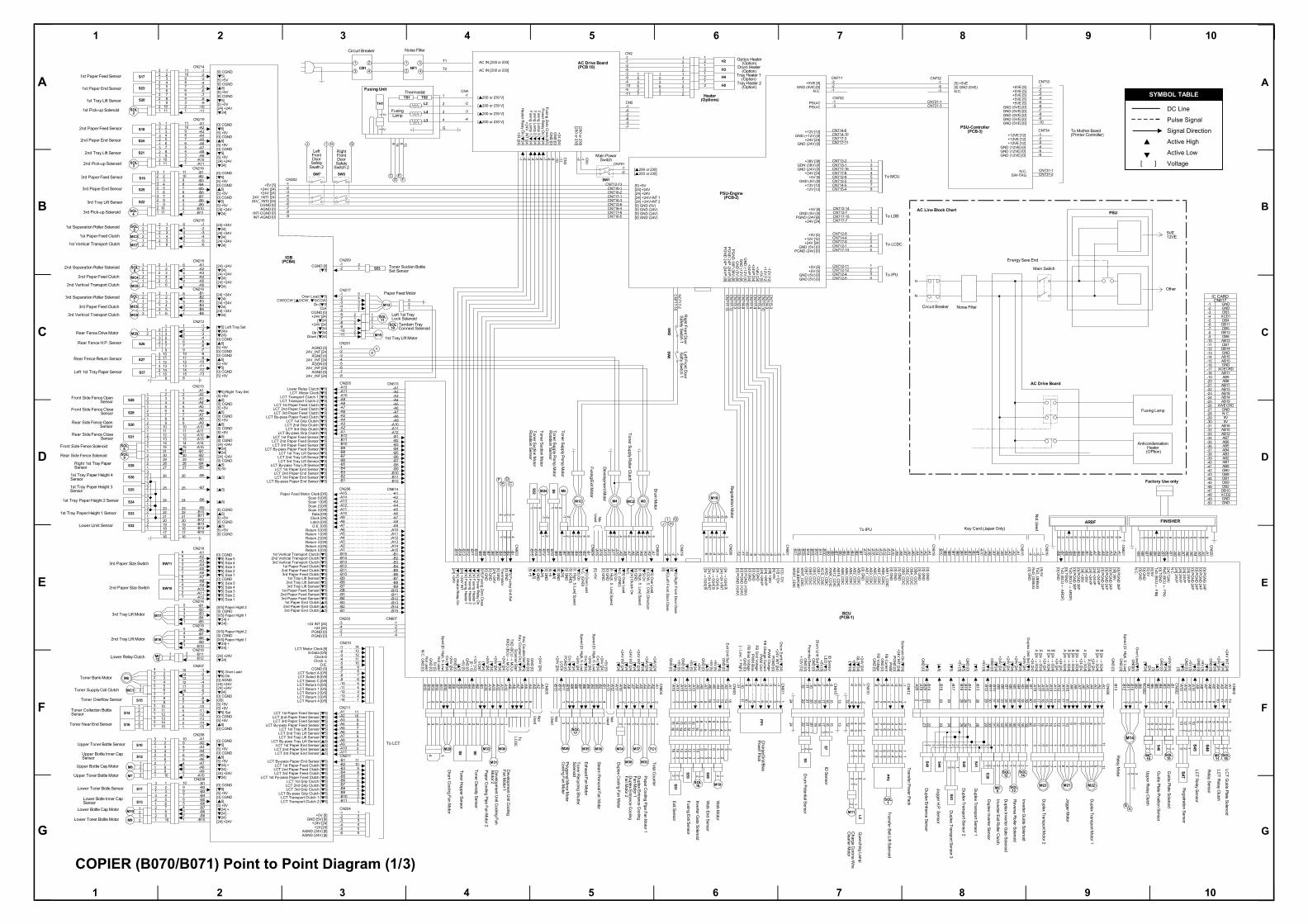
COPIER (B070/B071) Point to Point Diagram (1/3)
FusingLamp
["200 or 230 V]
["200 or 230 V]
["200 or 230 V]
["200 or 230 V]
DC Line
"
!
[ ]
Pulse Signal
Signal Direction
Active High
Voltage
SYMBOL TABLE
Active Low
Not U
sed
Registration M
otor
PP2
CGND [0][!5]
14
[5] +5VE
15 GND 1 GND 15 GND 1 GND14 GND 2 GND 14 GND 2 GND13 TXFCLK+ 3 TXFCLK+ 13 TXLCLK+ 3 TXLCLK+12 TXFCLK- 4 TXFCLK- 12 TXLCLK- 4 TXLCLK-11 GND 5 GND 11 GND 5 GND10 GND 6 GND 10 GND 6 GND9 TXFIN2+ 7 TXFOUT2+ 9 TXLIN2+ 7 TXLOUT2+8 TXFIN2- 8 TXFOUT2- 8 TXLIN2- 8 TXLOUT2-7 GND 9 GND 7 GND 9 GND6 GND 10 GND 6 GND 10 GND5 TXFIN1+ 11 TXFOUT1+ 5 TXLIN1+ 11 TXLOUT1+4 TXFIN1- 12 TXFOUT1- 4 TXLIN1- 12 TXLOUT1-3 GND 13 GND 3 GND 13 GND2 GND 14 GND 2 GND 14 GND1 GND 15 GND 1 GND 15 GND
CN313(LCDC) CN421(SBU) CN315(LCDC) CN422(SBU)
40 GND 1 GND39 SBU_CLK 2 SYCLK38 GND 3 GND37 XSDSCAN 4 XSDSCAN36 XSSCAN 5 XSSCAN35 XSLEAD 6 XSLEAD34 N.C. 7 LAMPGT33 GND 8 GND32 GND 9 GND31 +12V 10 +12V30 +12V 11 +12V29 +12V 12 +12V28 +12V 13 +12V27 GND 14 GND26 GND 15 GND25 SBU_DO 1624 GND 17 GND23 SBU_DI 1822 GND 19 GND21 GND 20 GND20 +5VF 21 +5V19 +5VF 22 +5V18 +5VF 23 +5V17 +5VF 24 +5V16 +5VF 25 +5V15 +5VF 26 +5V14 GND 27 GND13 GND 28 GND12 GND 29 GND11 GND 30 GND10 +5VF 31 +5V(3.3V)9 +5VF 32 +5V(3.3V)8 +5VF 33 +5V(3.3V)7 +5VF 34 +5V(3.3V)6 +5VF 35 +5V(3.3V)5 +5VF 36 +5V(3.3V)4 GND 37 GND3 GND 38 GND2 SBU_CSB 39 XSYCS1 GND 40 GND CN314(LCDC) CN423(SBU)
23 A1922 A14 45 GND21 A18 44 XCAD_SET220 A13 43 D1019 A17 42 D218 A8 41 D917 A9 40 D116 A11 39 D815 XCAD_RD 38 D014 GND 37 +3.3V13 A10 36 A112 D15 35 A211 D14 34 A310 D7 33 A49 D13 32 A58 D6 31 A67 D12 30 A76 D5 29 A125 D11 28 A154 D4 27 A163 XCAD_SET1 26 +5V2 D3 25 A201 GND 24 NC
50 +5VE 100 +5VE49 GND 99 GND48 PWRCTL0 98 PWRCTL147 GND 97 GND46 XPW_SW 96 OPREQ45 GND 95 GND44 OPTXD 94 OPRXD43 GND 93 GND42 OPTCLK 92 OPRCLK41 GND 91 GND40 N.C. 90 N.C.39 GND 89 GND38 GND 88 GND37 GND 87 GND36 GND 86 GND35 AD1 85 AD034 AD3 84 AD233 AD5 83 AD432 AD7 82 AD631 CBE0 81 GND30 AD9 80 AD829 AD11 79 AD1028 AD13 78 AD1227 AD15 77 AD1426 CBE1 76 GND25 XSERR 75 PAR24 XSTOP 74 XPERR23 XTRDY 73 XDEVSEL22 XFRAME 72 XIRDY21 XRST 71 GND20 CBE2 70 GND19 AD17 69 AD1618 AD19 68 AD1817 AD21 67 AD2016 AD23 66 AD2215 CBE3 65 GND14 AD25 64 AD2413 AD27 63 AD2612 AD29 62 AD2811 AD31 61 AD3010 XREQ 60 IDSEL9 GND 59 XGNT8 GND 58 GND7 GND 57 XINT6 GND 56 GND5 GND 55 GND4 GND 54 GND3 PCICLK 53 GND2 XENGRDY 52 N.C.1 GND 51 GND
CN807(RAPI)
PMSTRAT
GND -A1 -A2 -A3 -A4
BCU_A1BCU_A3BCU_A5
GND -A8 -A9-A10-A11
GNDGND
-A5 -A6 -A7
BCU_A7BCU_A9
BCU_D1 -B7 -B8 -B9-B10
BCU_CSBBCU_RDB
BCU_INTB -B3 -B4 -B5 -B6
BCU_D7BCU_D5BCU_D3
GND-A16-A17 -B1 -B2
GNDBCU_RESB
BCU_D2-A12-A13-A14-A15
BCU_D4BCU_D6GND
BCU_SLERB
BCU_D0
BCU_A11
BCU_A4-B15-B16-B17
BCU_A2BCU_A0
-B13-B14
BCU_A10BCU_A8BCU_A6
-B12-B11
BCU_WRBBCU_A12
+5V -2 -3 -4
GNDGND
-1 +5V
-A17-A16-A15-A14-A13
-A11-A10-A9-A8-A7
-A12
-B10-B9-B8-B7-B6
-B4-B3-B2-B1
-B5
-B14-B13-B12-B11
-A1-B17-B16-B15
-A3-A2
-A6-A5-A4
+24V+5VGNDGND
-1-2-3-4
1234
1234
-A1
-B9
-A2
-B8
-A3
-B7
-A4
-B6
-A5
-B5
-A6
-B4
LDD
0PLD
D0N
LDD
1PLD
D1N
LDD
2PLD
D2N
LDD
3PLD
D3N
LDD
4PLD
D4N
LDD
5PLD
D5N
LDD
6PLD
D6N
LDD
7PLD
D7N
GN
D G
ND
-A7
-B3
-A8
-B2
-A9
-B1
-A15
-A14
-A13
-A12
-A11
-A10 -A
9-A
8-A
7-A
6-A
5-A
4
XAPC
3
XAPC
2
XAPC
1
XAPC
0
AS
0
AS
1
AS
2
-A3
-A2
-A1
-B15
-B14
-B13
-B12
-B11
-B10 -B
9-B
8-B
7-B
6-B
5-B
4-B
3-B
2-B
1
A
S3
A
S5
A
S6
A
S7
PM
STR
AT
PMC
LKXS
CR
EAD
Y S
CLK
OU
T
SLO
AD S
DTO
UT
G
ND
A
S4
+24V [24] GND [0]
XSCREADY PMCLK
-1-2-3-4-5
-5-4-3-2-1
[24] 24V[0] GNDPMSTARTXSCREADPMCLK
-B14-B13-B12
[0] GNDOPTXDOPTCLK
[0] GND -B8 -B7 -B6 -B5
OPREQXPW_SW
-B11-B10 -B9
[0] GNDOPRCLK
TXFIN1-
-5 -6 -7 -8
TXLCLK+
TXFCLK-
-1 -2 -3 -4
TXFIN2+TXFIN2-TXFIN1+
SBU_CLK -B4 -B3 -B2 -B1
SBU_DOSBU_DISBU_CSB
TXFCLK+
OPRXD
GND -13 -14 GND
-11 -12
TXLIN2-TXLIN1+TXLIN1-
-10 -9
TXLCLK-TXLIN2+
-A14-A13
[0] GND
-A9 -A8 -A7 -A6
XFOOT_SWGND
-A12-A11-A10
[!5] Red PL_R[!5] Green PL_G
-A1
KEY_UP
-A5 -A4 -A3 -A2
SCANSTRATMCU_RXDMCU_TXD
KEY_SET
[24] +24V
XSSCAN -5 -4 -3
XSLEAD
RXD
-14 -13 -12
XAPS5[5] +5V
-2 -1
TXDGND
XAPS4 -11 -10 -9
[5] +5V[0] GND
[0] GND
-2
-6
[5] +5V -1
-7 XSDSCAN
FAN_TRG
-5-6-7-8-9
-11-12-13-14
-10
-1-2-3-4
-5-6-7-8-9
-11-12-13-14
-10
-1-2-3-4
-A3-A4
-A6-A7-A8-A9
-A5
-B1-B2-B3
-B5-B6-B7-B8
-B4
-8-9-10
-12-13-14-15
-11
-1-2
-4-5-6-7
-3
-7-8-9
-11-12-13-14
-10
-1
-3-4-5-6
-2
-6
-8
-1-2-3
-4-5
-3-4-5
-7-8-9-10
-6
-4-5-6
-1-2
-7
-1-2-3
-4-5
-2-3
-1
OPCLK_CN
-10 -9 -8 -7
[0] GND
AN_X_OUT
-13 -12 -11
AN_X_VCCOPDTOUT_CNOPDTIN_CN
AN_Y_OUT
-2 -1
-4 -3 [12] +12V
[5] +5V[5] +5V
-5 -6
[0] GND[12] +12V
AN_X_GND
-15 -14
AN_Y_GND
RXIN2-
-5 -6 -7 -8
[0] GND
RXCLK+ -2 -3 -4
RXCLK-[5] +5VRXIN2+
[0] GND
RXIN0- -13 -14 [3.3] +3.3V
-11 -12
RXIN1-[0] GNDRXIN0+
-10 -9
[0] GNDRXIN1+
-1
GND [0] TXOUT2-_OP
TXOUT2+_OP +5V [5]
TXCLK-_OP TXCLK+_OP GND [0]
+3.3V [3.3] TXOUT0-_OP
TXOUT0+_OP GND [0]
TXOUT1-_OP TXOUT1+_OP
GND [0]
OP_DO OP_DI
TP_P_X TP_P_Y
AN_TP_X AN_TP_Y TP_G_X
+5V [5] +5V [5]
+12V [12] +12V [12] GND [0] GND [0]
OPCLK
TP_G_Y
AN_Y_VCC
Length 1 [!5] +5V [5]
GND [0]
GND [0] +24V [24]
GND [0] NC
Length 2 [!5] +5V [5]
GND [0] GND [0]
NC
+24V [24] NC NC
KEY_UP +24V [24]
KEY_SET GND [0]
+5V [5] LED_Sleep [!5]
Operation Switch [!5] GND [0]
60FAN [!24]
24V_GND [0] +5V [5]
GND [0] +12V [12]
+24V [24]
LED_Power [!5]
GNDOPRXD
OPRCLKGND
OPTCLKOPTXD
GND
SBU_CSBSBU_DI
SBU_DOSBU_CLK
+5VEXPW_SW
OPREQ
RCLKPP1RBMP2RBPP2RCMP2RCPP2
RCLKMP2RCLKPP2
GNDGND
RBMP1RBPP1RCMP1RCPP1
RCLKMP1
APS5
GND MCU_TXD MCU_RXD
SCANSTRAT
NC NC NC NC
APS4 NC NC
XSLEAD XSSCAN
XSDSCAN
-A1-A2 NC
FAN_TRG
-1-2
-4-5-6
-3
-1-2
-1-2-3
-5-6-7-8
-4
-1-2-3
-2-3-4-5
-1
-4-5-6-7
-3
-1-2
-1-2 M
Width 1
+5V [5] ["5]
GND [0]
PGND [0] +24V [24]
ON ["24]
Width 3Width 2
-12V [12] +12V [12]
+24V [24] PGND [0]
MGND [0] +38V [38]
GND [0] +5V [5]
GND [0] +5V [5]
GND [0]
XLMP_EX
GND [0]XENCSET_GND
XSIZEX XHMG_EX
XSCAN_EX
SC_CW SC_CCW
XENCSET
ENC_A ENC_B
GND [0]
+5V [5]
12
123
4
4512
123
45
23
1
12345
M28
APS4
APS5
2 1
4 3
5
4 3
1
1 2
5
2 1
2 1
3 4
3 2
2 1
4 3
5 1
5 4
2 1
4 3
5
CN
807
CN
618
LDD
0PLD
D0N
LDD
1PLD
D1N
LDD
2PLD
D2N
LDD
3PLD
D3N
LDD
4PLD
D4N
LDD
5PLD
D5N
LDD
6PLD
D6N
LDD
7PLD
D7N
GND
GND
ANID
GND
FAN
ON
LDO
FFXD
ETP0
DR
OPE
NXL
DER
RAP
C7
APC
6AP
C5
APC
4AP
C3
APC
2AP
C1
APC
0AS
0AS
1AS
2AS
3
AS5
AS6
AS7
PMST
RAT
PMC
LKXS
CR
EAD
YSC
LKO
UT
SLO
ADSD
TOU
TG
ND
AS4
-A2
-A4
-A5
-A6
-A7
-A8
-A9
-A10
-A11
-A12
-A13
-A14
-A15
-B1
-B2
-B3
-B4
-B5
-B6
-B7
-B8
-B9
-B10
-B11
-B12
-B13
-B14
-B15
-A1
-B9
-A2
-B8
-A3
-B7
-A4
-B6
-A5
-B5
-A6
-B4
-A7
-B3
-A8
-B2
-A9
-B1
-A1
-A3
15 14 13 12 11 10 9 8 7 6 5 4 3 2 1 15 14 13 12 11 10 9 8 7 6 5 4 3 2 1
M2
CN
402
CN
804
CN
401
M27
FAN
+FA
N-
2 1
["5]
+5V_
SW
XDET
P0[5
] +5V
[0] G
ND
-1 -3 -5 -6 -7
2 1
1 2
3 2 1
CN802
56789
11121314
10
1234
1234
56
1234
5
10 9 8 7 6
4 3 2 1
5
14 13 12 11
2 1 2 1 6
4 3 2 1
5
3
CN302
CN311
CN555
CN559
CN557
CN
315
CN555
CN553
CN
314
CN
313
CN
422
CN
423
CN
421
CN551
CN552
CN560
CN561
CN556
CN305
CN306
CN301
CN309
CN310
CN316
34
678
5
-1-2
1
M25
1 2 3 4 5 6 7 8 9 10 11 12 13 14 15 1 2 3 4 5 6 7 8 9 10 11 12 13 14 15
2
345678
154321
32
12
3
54321
NCNCNC
A
DIN
G
ND
FA
NO
N
LDO
FF X
DET
P0 D
RO
PEN
XLD
ERR
XA
PC7
XA
PC5
XA
PC4
XA
PC6
-B9 NC
-7 2
CN21234
1234
To Mother Board
To BCU
To PSU-Engine
To PSU-Engine
LDB (PCB 9)
LDB
Coo
ling
Fan
Mot
or
Rig
ht F
ront
Doo
r Saf
ety
Switc
h 3
Left
Fron
t Doo
r Saf
ety
Switc
h 3
Lase
rSy
nchr
oniza
tion
Det
ecto
r Boa
rdPC
B 20
SW9
SW8
SW4
SW5
Rig
ht F
ront
Doo
r Saf
ety
Switc
h 4
Left
Fron
t Doo
r Saf
ety
Switc
h 4
Polygonal MirrorMotor Control
PCB 8
IPU (PCB 16)
LCDC (PCB 15)
Option Pannel(PCB 11)
SBU (PCB 5)
To PSU
S1
S2
Scanner Home Position Sensor
Original Width Sensors
Exposure LampLamp Regulator
PCB 7 L1
Factory Use
Scanner Motor
E
To PSU Engine
To Key Counter
Optics Cooling Fan Motor
OperationSwitch
(PCB 12)
SBU Cooling Fan Motor
S3
S4Original Length Sensor 2
Original Length Sensor 1
PolygonalMirrorMotor
To BCU
A
B
C
D
E
F
G
1 2 3 4 5 6 7 8 9 10
A
B
C
D
E
F
G
1 2 3 4 5 6 7 8 9 10
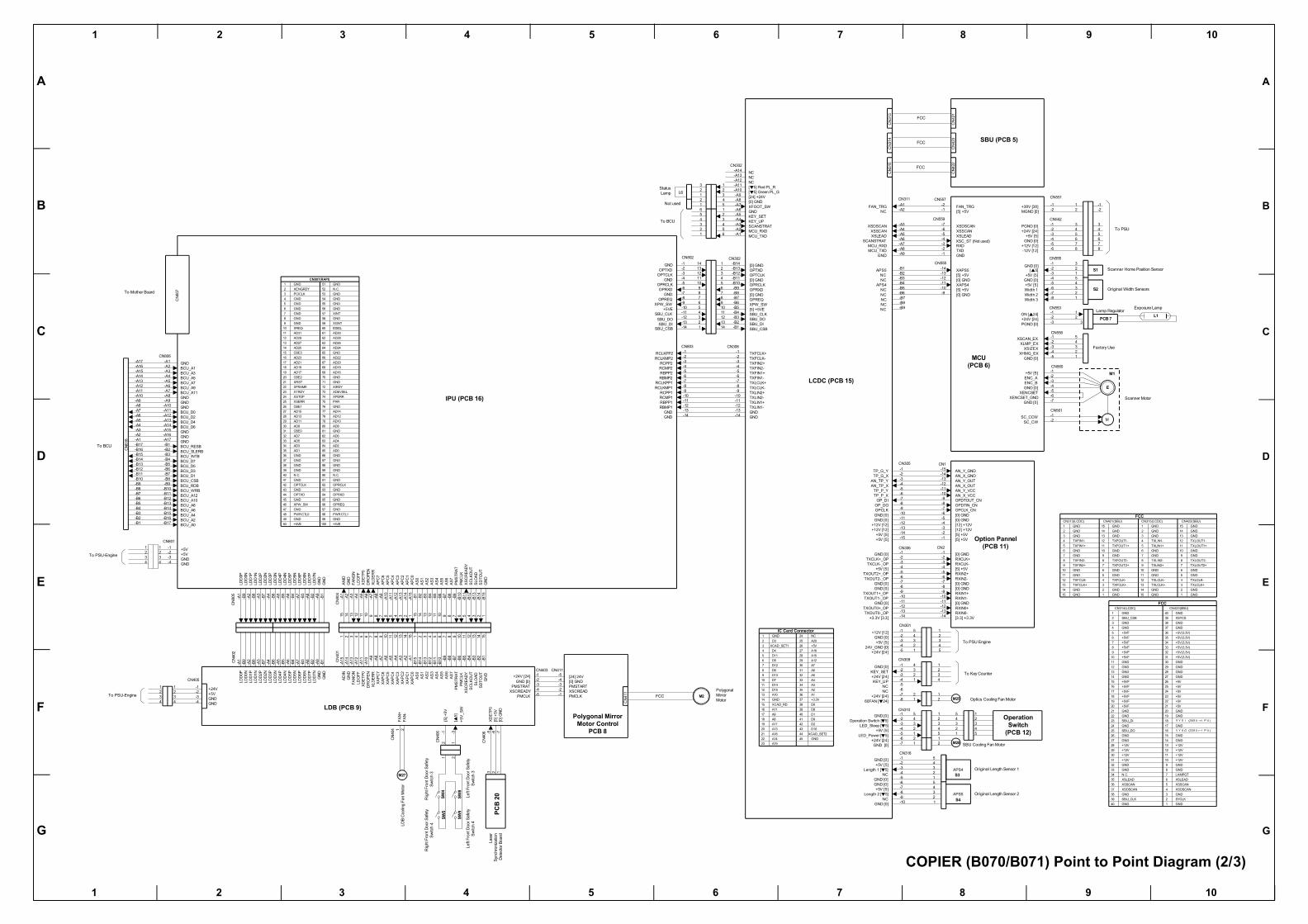
COPIER (B070/B071) Point to Point Diagram (2/3)
IC Card Connector
FCC
FCC
MCU(PCB 6)
XSC_ST (Not used)
L6StatusLamp
Not used
FCC
FCC
FCC
FCC
CN806
CN801
CN
404
CN
406
CN
406
[5] +
5V
CN403 CN411
CN
411
CN803 CN308
CN302
M1
CN1
CN405
CN
805
SD2_DT(2) 2 SD_CMD(2) 3 4 5 6 GND 7 8
SD_WP(2)#
9SD_CD(2)#10
11
1
12
GND3VAUXSDCLK2
SD2_DT(0)
GND
SD2_DT(1)SD2_DT(2)
SD1_DT(3) 2 SD_CMD(1) 3 4 5 6 GND 7 8
SD_WP(1)#
9SD_CD(1)#10
11
1
12
GND3VAUXSDCLK1
SD1_DT(0)
GND
SD1_DT(1)SD1_DT(2)
VCC12SENCE
GND
2 +
GND 2 VCC12 3
1
SENCE
VREF 2 VREF 3 4 5 6 7 8 91011
1
12
MDT(0)
1213
15161718
14
1920
2627282930
232425
202122
40
33343536
3839
37
3132
40414243
45464748
44
4950
GNDGND
MDT(4)MDT(1)MDT(5)VCC2.5VCC2.5
MDT(2)
GNDGNDMDT(6)
DQS_SR(0)DM_SR(0)
MDT(3)MDT(7)MDT(8)MDT(12)VCC2.5VCC2.5MDT(9)MDT(13)DQS_SR(1)DM_SR(1)
GNDGND
MDT(10)MDT(14)MDT(11)MDT(15)VCC2.5VCC2.5CLKOTH(1)
CLKOTL(1)VCC2.5
GNDGNDGNDMDT(16)MDT(20)MDT(17)MDT(21)VCC2.5VCC2.5DQS_SR(2)DM_SR(2)MDT(18)MDT(22)
GNDGND
MDT(19)MDT(23)MDT(24)MDT(28)VCC2.5VCC2.5
54555657
515253
64656667
60616263
5859
80818283
90919293
86878889
8485
76777879
72737475
68697071
96979899
9495
101102103104105106107108109
112113114115116117118119120121
110111
133134135136137
140141142143144145146147148149
138139
126127128
131132
129130
122123124125
150100
MDT(25)MDT(29)DQS_SR(3)DM_SR(3)
GNDGND
MDT(26)MDT(30)MDT(27)MDT(31)VCC2.5VCC2.5MECC_SR(0)MECC_SR(4)MECC_SR(1)MECC_SR(5)
GNDGND
DQS_SR(8)DM_SR(8)MECC_SR(2)MECC_SR(6)VCC2.5VCC2.5MECC_SR(3)MECC_SR(7)
NCNC
GNDGND
GNDCLKOTH(0)
CLKOTL(0)VCC2.5VCC2.5VCC2.5CKEA_SR#CKEA_SR#
NCA13:NC
MAA_SR(12)MAA_SR(11)
151152153154155156157158159
162163164165166167168169170171
160161
183184185186187
190191192193194195196197198199
188189
176177178
181182
179180
172173174175
200
MAA_SR(9)MAA_SR(8)
GNDGND
MAA_SR(7)MAA_SR(6)MAA_SR(5)MAA_SR(4)
VCC2.5VCC2.5MAA_SR(10)MAA_SR(14)MAA_SR(13)RASA_SR#
MAA_SR(3)MAA_SR(2)MAA_SR(1)MAA_SR(0)
WEA_SR#
CS_SR(0)#CS_SR(1)#NCNC
GNDGND
MDT(32)MDT(36)MDT(33)MDT(37)VCC2.5VCC2.5DQS_SR(4)DM_SR(4)MDT(34)MDT(38)
GNDGND
MDT(35)MDT(39)MDT(40)MDT(44)VCC2.5VCC2.5MDT(41)MDT(45)DQS_SR(5)DM_SR(5)
GNDGND
CASA_SR#
MDT(42)MDT(46)MDT(43)MDT(47)VCC2.5VCC2.5VCC2.5
GNDCLKOTL(2)
GNDCLKOTH(2)
GNDMDT(48)MDT(52)MDT(49)MDT(53)VCC2.5VCC2.5DQS_SR(6)DM_SR(6)MDT(50)MDT(54)
GNDGND
MDT(51)MDT(55)MDT(56)MDT(60)VCC2.5VCC2.5MDT(57)MDT(61)DQS_SR(7)DM_SR(7)
GNDGND
MDT(58)MDT(62)MDT(59)MDT(63)VCC2.5VCC2.5SMBUSDSA0SMBUSCSA1VCC2.5SA2
NCNC
32
4567891011
1
121213
1516
14
191817
20
2627282930
232425
2122
40
33343536
3839
37
3132
414243
45464748
44
4950
54555657
515253
60
5859
64656667
616263
686970
80
76777879
72737475
71
818283
868788
8485
GNDINTC#GND
GND
GND
GND
GND
GND
GND
AD(31)
RESERVED
CLKRUN
AD(30)AD(29)AD(28)
AD(26)GNDAD(25)AD(24)
AD(27)
PCIRST1#
PCICLK(3)
GNT(1)#
REQ(1)#
PCI_PME#
C_BE(3)GND
GND
GND
GND
GND
GND
GND
GND
GND
GND
AD(22)
AD(21)AD(20)AD(19)
AD(18)AD(17)AD(16)
AD(15)AD(14)
AD(13)AD(12)AD(11)
AD(10)AD(9)AD(8)
AD(7)AD(6)AD(5)AD(4)AD(3)AD(2)
AD(1)
AD(0)
VCC3.3
VCC3.3
VCC3.3
VCC3.3
VCC3.3
VCC3.3
VCC5
VCC5
RESERVED
IDSELAD(23)
C_BE(2)FRAME#IRDY#
TRDY#DEVSEL#STOP#
PERR#SERR#PAR
C_BE(1)
C_BE(0)
RESERVED
RESERVED
RESERVED
RESERVED
RESERVED3VAUXRESERVED
2 1
2627282930
232425
3 4 5 6 7 8 910111213
15161718
14
19202122
40
33343536
3839
37
3132
414243
45464748
44
49505152
65
58596061
6364
62
5657
666768
70717273
69
74757677
53
5554
88899091
93949596
92
979899
81828384
8687
85
787980
101102103104
100
105106107108109
112113114115116117118119120121
110111
122123124
133134135136137
140141142143144145146147148149
138139
126127128
131132
129130
125
150151152153154155156
SD0_DTOUT1SD0_DTOUT0SD0_DTOUT3SD0_DTOUT2GNDGNDSDCLK0SD0_CMDOUTGND
SD0_CMDOUTOEGND
GND
GNDGND
GND
GNDGND
GNDGND
GNDGND
GND
GNDGND
GND
GND
GND
GND
GND
GND
GND
GND
GNDGND
GND
GNDGND
GND
GND
GND
GNDGND
GNDGNDGNDGND
SD0_CMDINSD0_WP#SD0_DTOUTOESD0_DTIN3SD0_CD#SMBUSC
SMBUSCSD0_DTIN2PWRGD_EXTSD0_DTIN1OPMCLKOMPTCLK
GNDOPMLEDOPMTXDOPMRXDSD0_DTIN0OPMRREQ#PEACE_TXDPEACE_RXD
CSS_RXDOPMRST#
CSS_CTSCSS_TXDCSS_RTS
USBP0USBN0
EDGE1#EDGE2#
CSS_WUP#USBOC0#
PWRC0PWRC1#PCI_PME#WUP_PWRS W#
NCPCIRST0#INTA#
AGP_GNT#AGP_PIPE#
AGP_REQ#AGP_ST(1)
AGP_ST(0)AGP_ST(2)
AGP_RBF#NC
AGP_AD(30)AGP_AD(31)AGP_AD(28)AGP_AD(29)AGP_AD(26)AGP_AD(24)AGP_AD(27)AGP_AD(25)
AGP_TPDET#A_CBE(3)#
AGP_AD(22)AG_ADS(1)#
AG_ADS(1)AGP_AD(20)
AGP_AD(18)AGP_AD(21)AGP_AD(16)AGP_AD(23)AGP_AD(17)AGP_AD(19)
AGP_IRDY#AGP_FRAME#GNDAGP_DEVSEL#NC
AGP_STOP#VREF4X_INAGP_TRDY#GNDAGP_PARA_CBE(2)#
AGP_AD(13)A_CBE(1)#AGP_AD(11)AGP_SERR#
AGP_AD(14)
AGP_AD(15)AG_ADS(0)
AG_ADS(0)#
AGP_AD(10)A_CBE(0)#AGP_AD(12)
AGP_AD(7)AGP_AD(9)AGP_AD(8)AGP_AD(4)
AGP_AD(2)AGP_AD(5)AGP_AD(0)AGP_AD(6)
AGP_AD(1)
AGP_AD(3)AGPCLK1
5VAUX12VAUX5VAUX12VAUX5VAUX5VAUXVCC_AGP
3.3VAUX
VCC3.3VCC3.3
2 1
3 4 5 6 7 8 910
GNDGNDGNDGNDGNDGND
5VAUX5VAUX5VAUX5VAUX
2 1
3 4 5 6
12VAUX12VAUX12VAUXGNDGNDGND
2 1 XSW_TRG
90/105
CN140
2 1
2627282930
232425
3 4 5 6 7 8 910111213
15161718
14
19202122
40
33343536
3839
37
3132
414243
45464748
44
49505152
65
58596061
6364
62
5657
666768
70717273
69
74757677
53
5554
787980
888990
81828384
8687
85
91
93949596
92
979899
101102103104
100
105106107108109
112113114115116117118119120121
110111
122123124
133134135136137
140141142143144
138139
126127128
131132
129130
125
2 +
GND
MDQ0GND
MDQ32MDQ1MDQ33MDQ2MDQ34MDQ3MDQ35VCC3VCC3MDQ4MDQ36MDQ5MDQ37MDQ6MDQ38MDQ7MDQ39GNDGNDDQM0DQM4DQM1DQM5VCC3.3VCC3.3MA0MA3MA1MA4MA2MA5GNDGNDMDQ8MDQ40MDQ9MDQ41MDQ10MDQ42MDQ11MDQ43VCC3VCC3MDQ12MDQ44
MDQ13MDQ45MDQ14MDQ46MDQ15MDQ47GNDGNDNCNCNCNCCLK1CKE2VCC3VCC3RAS#CAS#RWE#CKE1CS1#MA12CS2#GNDNCCLK2GNDGNDNCNCNCNCVCC3VCC3MDQ16MDQ48MDQ17MDQ49MDQ18MDQ50MDQ19MDQ51GNDGNDMDQ20MDQ52MDQ21MDQ53
MDQ22MDQ54MDQ23MDQ55VCC3VCC3MA6MA7MA8BA0GNDGNDMA9BA1MA10MA11VCC3VCC3MDQ2DQM6MDQ3DQM7GNDGNDMDQ24MDQ56MDQ25MDQ57MDQ26MDQ58MDQ27MDQ59VCC3VCC3MDQ28MDQ60MDQ29MDQ61MDQ30MDQ62MDQ31
GNDGNDSDASCLVCC3VCC3
MDQ63
2 3 4 5 6 7 8 91011
1
1213
15161718
14
1920
32333435
37383940
36
262728293031
232425
2122
IDE1RST#GNDIDE1DB7IDE1DB8IDE1DB6IDE1DB9IDE1DB5IDE1DB10IDE1DB4IDE1DB11
IDE1DB13IDE1DB1IDE1DB14IDE1DB0IDE1DB15
IDE1DB3IDE1DB12IDE1DB2
GNDKEYPIN
GND
GND
GND
GND
GND
IDE1IORDYCSELIDE1DACK#
IDE1CS0#IDE1CS1#DASP
IDE1DRQ
IDE1IOW#
IDE1IOR#
IDE1INTRESERVEDIDE1AD1PDIAG#IDE1AD0IDE1AD2
3 G
ND
2 3 4 5 6 7 8 91011
1
1213
15161718
14
1920
32333435
37383940
36
262728293031
232425
2122
IDE2RST#GNDIDE2DB7IDE2DB8IDE2DB6IDE2DB9IDE2DB5IDE2DB10IDE2DB4IDE2DB11
IDE2DB13IDE2DB1IDE2DB14IDE2DB0IDE2DB15
IDE2DB3IDE2DB12IDE2DB2
GNDKEYPIN
GND
GND
GND
GND
GND
IDE2IORDYCSELIDE2DACK#
IDE2CS0#IDE2CS1#DASP
IDE2DRQ
IDE2IOW#
IDE2IOR#
IDE2INTRESERVEDIDE2AD1PDIAG#IDE2AD0IDE2AD2
2 1
3 4
VCC12GNDGNDVCC5
2 1
3 4 5 6
5VAUXCSSRXDCSSTXDGNDCSSCTSCSSRST#
1 +
2 1
3 4 5 6
5VAUX5VAUXPETXDPERXDGNDGND
2 G
ND
2 3 4 5 6 7 8 91011
1
121213
15161718
14
1920
2627282930
232425
202122
40
33343536
3839
37
3132
40414243
45464748
44
4950
54555657
515253
64656667
60616263
5859
80818283
90919293
86878889
8485
76777879
72737475
68697071
96979899
9495
100
GND
GNDGNDGNDGNDGNDGNDREQ1#AD31AD29AD27AD25C_BE3AD23AD21AD19AD17C_BE2
ENGRDY#CLK1
TRDY#STOP#SERR#C_BE1AD15AD13
FRAME#RST#
AD11AD9C_BE0AD7AD5AD3AD1GNDGNDGNDGNDNCGNDOPTCLKGNDOPTXDGND
GND
GND
GND
GNDGNDGNDGND
GND
GND
GNDGND
GND
GND
GNDGNDGND
GND
GND
GND
GND
GND
PW_SW#
PWRCTL0#
5VAUX
NC
INT1#
GNT1#IDSELAD30AD28AD26AD24
AD20AD18AD16
AD22
IRDY#DEVSEL#PERR#PAR
AD12AD10AD8
AD14
AD6
AD2AD0
AD4
GND
NC
5VAUX
PWRCTL1#
OPREQ
OPRXD
OPRCLK
2 3 4 5 6 7 8 91011
1
121213
15161718
14
1920
2627282930
232425
202122
40
33343536
3839
37
3132
40414243
45464748
44
4950
54555657
515253
64656667
60616263
5859
80818283
90919293
86878889
8485
76777879
72737475
68697071
96979899
9495
100
RESERVEDRESERVEDRESERVEDRESERVEDRESERVEDRESERVED
RESERVEDAD0
AD2AD1AD4AD6AD8C_BE0AD15AD10AD14AD13GNDGNDPARC_BE1STOP#PERR#IRDY#TRDY#AD16C_BE2AD19AD18AD22AD21C_BE3IDSEL_SL2AD26AD25AD30AD28PME#GNDGNDGNDCLKRUNRST#
GNDREQ_SL2#
PCLK_SL2#GNT_SL2#INTA_SL2#NC
VCC53VAUXVCC3VCC5VCC3VCC3VCC3VCC3
VCC3AD3
AD7AD5AD9GND
GND
GND
GNDGND
GND
GND
GND
GND
GND
GND
GND
GND
GNDGND
GNDGNDGND
GND
NC
AD12
AD15
SERR#
DEVSEL#
FRAME#
AD17
AD20
AD23
AD24IDSEL_SL1AD27
AD31AD29
PCLK_SL1GNT_SL1#INTA_SL1#
REQ_SL1#
CN134
2 3 4 5 6 7 8 91011
1
121213
15161718
14
1920
2627282930
232425
202122
40
33343536
3839
37
3132
40414243
45464748
44
4950
54555657
515253
60
5859
64656667
616263
686970
80
76777879
72737475
71
818283
868788
8485
GNDINTA_SL1#GND
GND
GND
GND
GND
GND
GND
AD31
INTB_SL1#
CLKRUN
AD30AD29AD28
AD26GNDAD25AD24
AD27
RST#
PCLK_SL1
GNT_SL1#
REQ_SL1#
PME#
C_BE3GND
GND
GND
GND
GND
GND
GND
GND
GND
GND
AD22
AD21AD20AD19
AD18AD17AD16
AD15AD14
AD13AD12AD11
AD10AD9AD8
AD7AD6AD5AD4AD3AD2
AD1
AD0
VCC3
VCC3
VCC3
VCC3
VCC3
VCC3
VCC5
VCC5
RESERVED
IDSEL_SL1AD23
C_BE2FRAME#IRDY#
TRDY#DEVSEL#STOP#
PERR#SERRPAR
C_BE1
C_BE0
RESERVED
RESERVED
RESERVED
RESERVED
RESERVED3VAUXRESERVED
CN151
2 3 4 5 6 7 8 91011
1
121213
15161718
14
1920
2627282930
232425
202122
40
33343536
3839
37
3132
40414243
45464748
44
4950
54555657
515253
60
5859
64656667
616263
686970
80
76777879
72737475
71
818283
868788
8485
GNDINTA_SL2#GND
GND
GND
GND
GND
GND
GND
AD31
INTB_SL2#
CLKRUN
AD30AD29AD28
AD26GNDAD25AD24
AD27
RST#
PCLK_SL2
GNT_SL2#
REQ_SL2#
PME#
C_BE3GND
GND
GND
GND
GND
GND
GND
GND
GND
GND
AD22
AD21AD20AD19
AD18AD17AD16
AD15AD14
AD13AD12AD11
AD10AD9AD8
AD7AD6AD5AD4AD3AD2
AD1
AD0
VCC3
VCC3
VCC3
VCC3
VCC3
VCC3
VCC5
VCC5
RESERVED
IDSEL_SL2AD23
C_BE2FRAME#IRDY#
TRDY#DEVSEL#STOP#
PERR#SERRPAR
C_BE1
C_BE0
RESERVED
RESERVED
RESERVED
RESERVED
RESERVED3VAUXRESERVED
234567891011
1
1213
15161718
14
1920
2627282930
232425
2122
40
33343536
3839
37
3132
414243
45464748
44
4950
54555657
515253
60
5859
64656667
616263
686970
80
76777879
72737475
71
818283
868788
8485
GNDINTD#GND
GND
GND
GND
GND
GND
GND
AD(31)
RESERVED
CLKRUN
AD(30)AD(29)AD(28)
AD(26)GNDAD(25)AD(24)
AD(27)
PCIRST1#
PCICLK(5)
GNT(2)#
REQ(2)#
PCI_PME#
C_BE(3)GND
GND
GND
GND
GND
GND
GND
GND
GND
GND
AD(22)
AD(21)AD(20)AD(19)
AD(18)AD(17)AD(16)
AD(15)AD(14)
AD(13)AD(12)AD(11)
AD(10)AD(9)AD(8)
AD(7)AD(6)AD(5)AD(4)AD(3)AD(2)
AD(1)
AD(0)
VCC3.3
VCC3.3
VCC3.3
VCC3.3
VCC3.3
VCC3.3
VCC5
VCC5
RESERVED
IDSELAD(23)
C_BE(2)FRAME#IRDY#
TRDY#DEVSEL#STOP#
PERR#SERR#PAR
C_BE(1)
C_BE(0)
RESERVED
RESERVED
RESERVED
RESERVED
RESERVED3VAUXRESERVED
2 3 4 5 6 7 8 91011
1
121213
15161718
14
1920
2627282930
232425
202122
40
33343536
3839
37
3132
40414243
45464748
44
4950
54555657
515253
60
5859
64656667
616263
686970
80
76777879
72737475
71
818283
868788
8485
GNDINTC#GND
GND
GND
GND
GND
GND
GND
AD(31)
RESERVED
CLKRUN
AD(30)AD(29)AD(28)
AD(26)GNDAD(25)AD(24)
AD(27)
PCIRST2#
PCICLK(2)
GNT(3)#
REQ(3)#
PCI_PME#
C_BE(3)GND
GND
GND
GND
GND
GND
GND
GND
GND
GND
AD(22)
AD(21)AD(20)AD(19)
AD(18)AD(17)AD(16)
AD(15)AD(14)
AD(13)AD(12)AD(11)
AD(10)AD(9)AD(8)
AD(7)AD(6)AD(5)AD(4)AD(3)AD(2)
AD(1)
AD(0)
VCC3.3
VCC3.3
VCC3.3
VCC3.3
VCC3.3
VCC3.3
VCC5
VCC5
RESERVED
IDSELAD(23)
C_BE(2)FRAME#IRDY#
TRDY#DEVSEL#STOP#
PERR#SERR#PAR
C_BE(1)
C_BE(0)
RESERVED
RESERVED
RESERVED
RESERVED
RESERVED3VAUXRESERVED
2 3 4 5 6 7 8 91011
1
121213
15161718
14
1920
2627282930
232425
202122
40
33343536
3839
37
3132
40414243
45464748
44
4950
54555657
515253
60
5859
64656667
616263
686970
80
76777879
72737475
71
818283
868788
8485
GNDINTD#GND
GND
GND
GND
GND
GND
GND
AD(31)
RESERVED
CLKRUN
AD(30)AD(29)AD(28)
AD(26)GNDAD(25)AD(24)
AD(27)
PCIRST2#
PCICLK(1)
GNT(4)#
REQ(4)#
PCI_PME#
C_BE(3)GND
GND
GND
GND
GND
GND
GND
GND
GND
GND
AD(22)
AD(21)AD(20)AD(19)
AD(18)AD(17)AD(16)
AD(15)AD(14)
AD(13)AD(12)AD(11)
AD(10)AD(9)AD(8)
AD(7)AD(6)AD(5)AD(4)AD(3)AD(2)
AD(1)
AD(0)
VCC3.3
VCC3.3
VCC3.3
VCC3.3
VCC3.3
VCC3.3
VCC5
VCC5
RESERVED
IDSELAD(23)
C_BE(2)FRAME#IRDY#
TRDY#DEVSEL#STOP#
PERR#SERR#PAR
C_BE(1)
C_BE(0)
RESERVED
RESERVED
RESERVED
RESERVED
RESERVED3VAUXRESERVED
CN101
(N
.C.)
(N.C.)
RAPI OPTION
(PIE
CE)
PCI OPTION
CN102
(CN
111)
3 G
ND
CN113
CN
160
CN114
CN131
CN
133
CN
147
CN807
CN132
CN150
CN134 CN149
CN143CN144
4 5V
HD
D3
GN
D2
GN
D1
12VH
DD
4 5V
HD
D3
GN
D2
GN
D1
12VH
DD
CN734CN733 CN001CN404CN731
K7_CORE 2 1
2627282930
232425
3 4 5 6 7 8 910111213
15161718
14
19202122
5657585960
535455
40414243
45464748
44
49505152
33343536
3839
37
3132K7_CORE
K7_COREK7_CORE
K7_COREK7_COREK7_COREK7_CORE
K7_CORE
K7_COREK7_COREK7_COREK7_CORE
K7_COREK7_COREK7_COREK7_CORE
K7_CORE
K7_COREK7_COREK7_COREK7_CORE
K7_COREK7_CORE
K7_COREK7_COREK7_COREK7_CORE
K7_COREK7_CORE
GNDGNDGNDGND
GNDCOREFB#
COREFBGND
VID(0)GNDGND
GNDGND
GNDGND
GNDGNDGNDGNDVCC12VCC12VCC12VCC12VCC12VCC12
RUN/SS
VID(1)VID(2)
VID(3)VID(4)
CPU CORE I/FPin# Signal Name Pin# Signal Name
VREF 2 VREF 3 4 5 6 7 8 91011
1
12
MDT(0)
1213
15161718
14
1920
2627282930
232425
202122
40
33343536
3839
37
3132
40414243
45464748
44
4950
GNDGND
MDT(4)MDT(1)MDT(5)VCC2.5VCC2.5
MDT(2)
GNDGNDMDT(6)
DQS_SR(0)DM_SR(0)
MDT(3)MDT(7)MDT(8)MDT(12)VCC2.5VCC2.5MDT(9)MDT(13)DQS_SR(1)DM_SR(1)
GNDGND
MDT(10)MDT(14)MDT(11)MDT(15)VCC2.5VCC2.5CLKOTH(4)
CLKOTL(4)VCC2.5
GNDGNDGNDMDT(16)MDT(20)MDT(17)MDT(21)VCC2.5VCC2.5DQS_SR(2)DM_SR(2)MDT(18)MDT(22)
GNDGND
MDT(19)MDT(23)MDT(24)MDT(28)VCC2.5VCC2.5
54555657
515253
64656667
60616263
5859
80818283
90919293
86878889
8485
76777879
72737475
68697071
96979899
9495
101102103104105106107108109
112113114115116117118119120121
110111
133134135136137
140141142143144145146147148149
138139
126127128
131132
129130
122123124125
150100
MDT(25)MDT(29)DQS_SR(3)DM_SR(3)
GNDGND
MDT(26)MDT(30)MDT(27)MDT(31)VCC2.5VCC2.5MECC_SR(0)MECC_SR(4)MECC_SR(1)MECC_SR(5)
GNDGND
DQS_SR(8)DM_SR(8)MECC_SR(2)MECC_SR(6)VCC2.5VCC2.5MECC_SR(3)MECC_SR(7)
NCNC
GNDGND
GNDCLKOTH(3)
CLKOTL(3)VCC2.5VCC2.5VCC2.5CKEB_SR#CKEB_SR#
NCA13:NC
MAB_SR(12)MAB_SR(11)
151152153154155156157158159
162163164165166167168169170171
160161
183184185186187
190191192193194195196197198199
188189
176177178
181182
179180
172173174175
200
MAB_SR(9)MAB_SR(8)
GNDGND
MAB_SR(7)MAB_SR(6)MAB_SR(5)MAB_SR(4)
VCC2.5VCC2.5MAB_SR(10)MAB_SR(14)MAB_SR(13)RASB_SR#
MAB_SR(3)MAB_SR(2)MAB_SR(1)MAB_SR(0)
WEB_SR#
CS_SR(2)#CS_SR(3)#NCNC
GNDGND
MDT(32)MDT(36)MDT(33)MDT(37)VCC2.5VCC2.5DQS_SR(4)DM_SR(4)MDT(34)MDT(38)
GNDGND
MDT(35)MDT(39)MDT(40)MDT(44)VCC2.5VCC2.5MDT(41)MDT(45)DQS_SR(5)DM_SR(5)
GNDGND
CASB_SR#
MDT(42)MDT(46)MDT(43)MDT(47)VCC2.5VCC2.5VCC2.5
GNDCLKOTL(5)
GNDCLKOTH(5)
GNDMDT(48)MDT(52)MDT(49)MDT(53)VCC2.5VCC2.5DQS_SR(6)DM_SR(6)MDT(50)MDT(54)
GNDGND
MDT(51)MDT(55)MDT(56)MDT(60)VCC2.5VCC2.5MDT(57)MDT(61)DQS_SR(7)DM_SR(7)
GNDGND
MDT(58)MDT(62)MDT(59)MDT(63)VCC2.5VCC2.5SMBUSDSA0SMBUSCSA1VCC2.5SA2
NCNC
Pin# Signal Name DDR-SDRAM DIMM I/FPin# Signal Name Pin# Signal Name Pin# Signal Name
CN101
1 SI
GN
AL
CONTROLLER-MOTHER I/FPin# Signal Name Pin# Signal Name
1 SI
GN
AL
Pin# Signal Name
Pin# Signal Name DDR-SDRAM DIMM I/FPin# Signal Name Pin# Signal Name Pin# Signal Name
CN102PCI OPTION I/F
Pin A# Signal Name Pin B# Signal Name
CN103PCI OPTION I/F
Pin A# Signal Name Pin B# Signal Name
CN105
SDRAM I/FPin# Signal Name Pin#
ENGINE I/FCN132
RAPI OPTION I/FPin# Signal Name Pin# Signal Name
Pin A# Signal Name Pin B#
Pin#
Signal Name
A
B
C
D
E
F
G
1 2 3 4 5 6 7 8 9 10
A
B
C
D
E
F
G
1 2 3 4 5 6 7 8 9 10
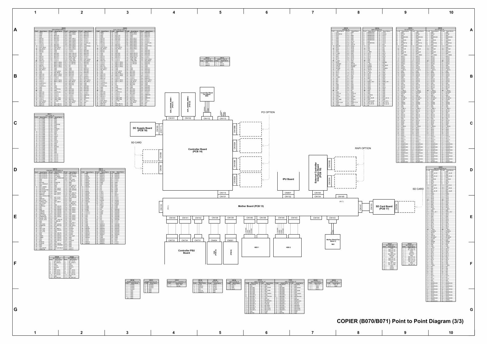
COPIER (B070/B071) Point to Point Diagram (3/3)
CN111
CN114 CN113
CN109 CN108SD CARD I/F SD CARD I/F
Pin# Signal Name Pin# Signal Name
Signal NamePin#POWER SUPPLY I/F
CN141
Signal NamePin#POWER SUPPLY I/F
CN141
Signal NamePin#POWER SUPPL Y CONTROL I/F
CN138 CN139CSS I/F PEACE I/F
Signal NamePin# Signal NamePin#
CN146HDD POWER I/F
Signal NamePin#
CN135HDD CONTROL I/F
Signal NamePin# Signal NamePin#
CN36HDD CONTROL I/F
Signal NamePin# Signal NamePin#
CN145HDD POWER I/F
Signal NamePin#1234
VCC 12GNDGND
VCC 5
CN143CASE FAN I/F
12
VCC 12GND
Pin# Signal Name
CN112 CN113CPU FAN I/F AMD761 FAN I/F
Signal Name Pin# Signal Name
2 3
1
Pin# Signal Name Pin# Signal Name
CN147 CN154SD CARD I/F SD CARD I/F
Pin# Signal Name Pin# Signal Name123456789
101112131415
GNDSD0_DT (2)SD0_DT (3)
GNDSD_SMD (0)
SDCLK0GND
SD0_DT (0)SD0_DT (0)
GNDSD_WP (0)#SD_CD (0)#
GND3VAUX3VAUX
123456789
101112
SD0_DT (3)SD_CMD (0)
GND3VAUX
SDCLK0GND
SD0_DT (0)SD0_DT (1)SD0_ DT (2)SD_CD (0)
GNDSD_WP (0)
Controller Board(PCB 14)
Controller BoardFan Motor
M39
Controller PSUBoard C
SS(P
CB 2
3)
HDD 1 HDD 2
Mother Board (PCB 13)
Mother Board FanMotor 2
M41
SD Card Board(PCB 17)C
N15
3
CN143CN144CN136CN146CN139CN141CN140 CN142 CN138
CN112
IPU Board
Exte
rnal
Con
trolle
rIn
terf
ace
Boar
d(P
CB
19)
Signal Name Pin# Signal Name
RAPI EXTENSION I/F
SD CARD
DC Supply Board(PCB 18)
DD
R_S
DRA
M_D
IMM
1(P
CB 2
1)
DD
R_S
DRA
M_D
IMM
2(P
CB 2
2)
CN
108
CN
109
CN
103A
CN
103B
CN
105A
CN
105B
CN
151A
CN
151B
CN
154
SD CARD
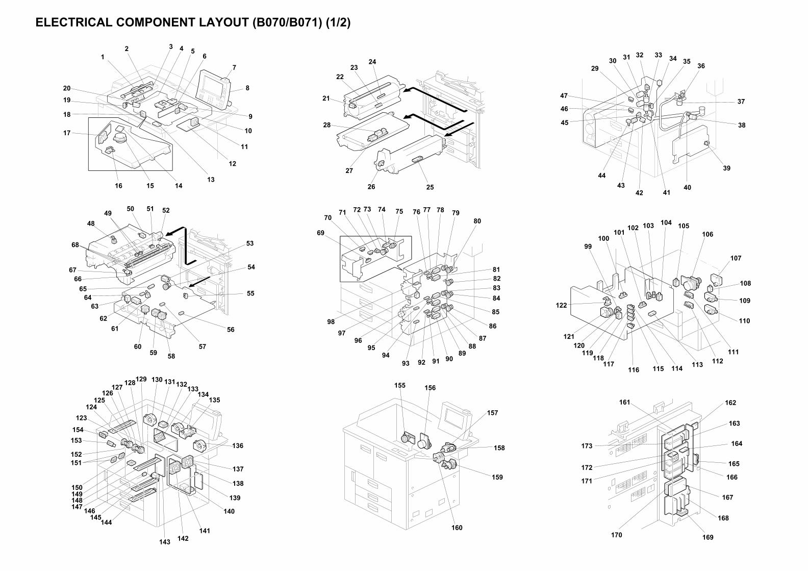
ELECTRICAL COMPONENT LAYOUT (B070/B071) (1/2)
16
17
18
1920
12 3 4 5
67
8
9
10
11
12
131415
2423
22
21
27
26 25
2930
47
46
45
4443
42 4140
39
38
37
3635333231 34
99100
101 102 103 104 105106
107
108
109
110
111112113114115116
117118
119120
121
122
173
161 162
163
164
165
166
167
168
169170
171
172
155 156
157
158
159
160
69
7071 72 73 74 75 76 77 78 79
80
81828384
85
86
8788
8990919293
9495
9697
98
4849 50 51
53
54
55
6766
6564
63
6261
6059 58
57
56
68
52
28
123124
125126
127 128129 130 131132133134
135
136
137
139
140
141142143
144145
146147148149
151152
153154
150 138

ELECTRICAL COMPONENT LAYOUT (B070/B071) (2/2)
Symbol Index No. Description P to P Page Motors
M1 1 Scanner C9 ~ D9 2/3 M2 15 Polygonal Mirror F6 2/3 M3 156 Drum D5 1/3 M4 157 Development D5 1/3 M5 37 Toner Supply Pump D5 1/3 M6 41 Toner Bank F1 1/3 M7 33 Upper Toner Bottle G1 1/3 M8 31 Upper Bottle Cap F1 1/3 M9 47 Lower Toner Bottle G1 1/3
M10 30 Lower Bottle Cap G1 1/3 M11 21 Charge Corona Wire Cleaner G7 1/3 M12 155 Fusing/Exit D5 1/3 M13 106 Paper Feed C3 1/3 M14 159 Relay F9 1/3 M15 107 1st Tray Lift C3 1/3 M16 109 2nd Tray Lift E1 1/3 M17 110 3rd Tray Lift E1 1/3 M18 160 Registration D6 1/3 M19 67 Web G6 1/3 M20 121 Rear Fence Drive C1 1/3 M21 60 Jogger G9 1/3 M22 59 Duplex Transport 1 G9 1/3 M23 58 Duplex Transport 2 G9 1/3 M24 38 Toner Suction D5 1/3 M25 11 Optics Cooling Fan F8 2/3
M26 18 Polygonal Mirror Motor Cooling Fan F5 1/3
M28 10 SBU Cooling Fan F8 2/3 M29 136 Drum Cooling Fan F4 1/3 M30 142 Development Unit Cooling Fan 1 F4 1/3 M31 137 Development Unit Cooling Fan 2 F4 1/3 M32 133 Paper Cooling Pipe Fan 1 F5 1/3 M33 132 Paper Cooling Pipe Fan 2 F4 1/3 M34 149 Duplex Cooling Fan F5 1/3 M35 134 Exhaust Fan F5 1/3 M36 130 Steam Removal Fan F5 1/3 M37 151 Duplex Entrance Cooling Fan 1 F5 1/3 M38 154 Duplex Entrance Cooling Fan 2 F5 1/3 M39 171 Controller Board Fan B5 3/3 M40 169 Mother Board Fan 1 F7 3/3 M42 140 PSU Cooling Fan 1 - - M43 141 PSU Cooling Fan 2 - -
Symbol Index No. Description P to P Page Sensors
S1 19 Scanner HP C9 2/3 S2 4 Original Width C9 2/3 S3 5 Original Length 1 F8 2/3 S4 9 Original Length 2 G8 2/3 S5 24 Drum Potential F7 1/3 S6 25 Toner Density (TD) F4 1/3 S7 23 Image Density (ID) F7 1/3 S8 26 Toner Hopper F4 1/3
S9 36 Toner Supply Pump Motor Rotation D5 1/3
S10 29 Upper Toner Bottle F1 1/3 S11 46 Lower Toner Bottle G1 1/3 S12 32 Upper Bottle Inner Cap F1 1/3 S13 35 Lower Bottle Inner Cap G1 1/3 S14 44 Toner Collection Bottle F1 1/3 S15 45 Toner Overflow F1 1/3 S16 42 Toner Near End F1 1/3 S17 76 1st Paper Feed A1 1/3 S18 96 2nd Paper Feed A1 1/3 S19 92 3rd Paper Feed B1 1/3 S20 77 1st Tray Lift A1 1/3 S21 94 2nd Tray Lift B1 1/3 S22 91 3rd Tray Lift B1 1/3 S23 98 1st Paper End A1 1/3 S24 95 2nd Paper End A1 1/3 S25 93 3rd Paper End B1 1/3 S26 100 Rear Fence HP C1 1/3 S27 101 Rear Fence Return C1 1/3 S28 120 Front Side Fence Open D1 1/3 S29 99 Front Side Fence Closed D1 1/3 S30 103 Rear Side Fence Open D1 1/3 S31 102 Rear Side Fence Closed D1 1/3 S32 116 Lower Limit D1 1/3 S33 114 1st Tray Paper Height 1 D1 1/3 S34 118 1st Tray Paper Height 2 D1 1/3 S35 115 1st Tray Paper Height 3 D1 1/3 S36 117 1st Tray Paper Height 4 D1 1/3 S37 122 Left 1st Tray Paper C1 1/3 S38 113 Right 1st Tray Paper D1 1/3 S39 61 Duplex Inverter F8 1/3 S40 65 Duplex Entrance F8 1/3 S41 64 Duplex Transport 1 F8 1/3 S42 57 Duplex Transport 2 F8 1/3 S43 56 Duplex Transport 3 G8 1/3 S44 55 Jogger HP F8 1/3 S45 71 LCT Relay F10 1/3 S46 69 Relay F10 1/3 S47 70 Registration G10 1/3 S48 72 Guide Plate Position F10 1/3 S49 66 Web End G6 1/3 S50 51 Fusing Exit G6 1/3 S51 48 Exit G6 1/3 S52 40 Toner Suction Motor Rotation D5 1/3 S53 39 Toner Suction Bottle Set B3 1/3
Symbol Index No. Description P to P Page PCBs
PCB1 131 BCU D4,F4 ~ E10,F10 1/3
PCB2 138 PSU-Engine B6 1/3 PCB3 168 PSU-Controller A8 ~ B8 1/3
PCB4 139 IOB A2,A3 ~ G2,G3 1/3
PCB5 6 SBU A8 ~ B8 2/3 PCB6 20 MCU B8 ~ D8 2/3 PCB7 3 Lamp Regulator C9 2/3
PCB8 14 Polygonal Mirror Motor Control Board F5 2/3
PCB9 17 LDB F2 ~ F4 2/3 PCB10 143 AC Drive Board A5 1/3 PCB11 8 Operation Panel D8 ~ E8 2/3 PCB12 13 Operation Switch Board F8 2/3 PCB13 163 Mother Board E4 ~ E8 3/3
PCB14 166 Controller Board C4,C5 ~ D4,D5 3/3
PCB15 12 LCDC A7 ~ G7 2/3
PCB16 161 IPU B2,B6 ~ E2,E6 2/3
PCB17 162 SD Card Board E8 ~ E9 3/3 PCB18 172 DC Supply Board C3 3/3
PCB19 173 External Controller Interface Board D7 3/3
PCB20 16 Laser Synchronization Detector Board G4 2/3
PCB21 164 DDR � SDRAM-DIMM 1 C4 3/3 PCB22 167 DDR � SDRAM-DIMM 2 C4 3/3 PCB23 165 CSS Board F5 3/3
Symbol Index No. Description P to P Page Lamps
L1 2 Exposure Lamp C10 1/3 L2 68 Fusing Lamp 1 A4 1/3 L3 68 Fusing Lamp 2 A4 1/3 L4 68 Fusing Lamp 3 A4 1/3 L5 22 Quenching Lamp G7 1/3 L6 7 Status Lamp B6 2/3
Symbol Index No. Description P to P Page Power Packs
PP1 135 CGB (Charge, Grid, Bias) F6 1/3 PP2 28 Transfer G7 1/3
Symbol Index No. Description P to P Page Others
CB1 147 Circuit Breaker A4 1/3
H2 123 Optics Anti-condensation Heater (option) A6 1/3
H3 148 Drum Anti-condensation Heater (option) A6 1/3
H4 145 Tray Anti-Condensation Heater 1 (option) A6 1/3
H5 144 Tray Anti-Condensation Heater 2 (option) A6 1/3
HDD 1 167 HDD 1 E6 3/3 HDD 2 170 HDD 2 E6 3/3 NF1 146 Noise Filter A4 1/3 TC1 153 Total Counter F5 1/3 TH1 52 Fusing Thermistor A4 1/3 TS1 49 Thermostat 1 A4 1/3 TS2 49 Thermostat 2 A4 1/3
Symbol Index No. Description P to P page Switches
SW1 154 Main Power B5 1/3 SW2 127 Right Front Door Safety 1 C6 1/3 SW3 150 Right Front Door Safety 2 B3 1/3 SW4 128 Right Front Door Safety 3 G4 2/3 SW5 129 Right Front Door Safety 4 G4 2/3 SW6 124 Left Front Door Safety 1 C6 1/3 SW7 152 Left Front Door Safety 2 B3 1/3 SW8 125 Left Front Door Safety 3 G4 2/3 SW9 126 Left Front Door Safety 4 G4 2/3
SW10 111 2nd Tray Paper Size E2 1/3 SW11 112 3rd Tray Paper Size E2 1/3
Symbol Index No. Description P to P Page Solenoids
SOL1 27 Transfer Belt Lift G7 1/3 SOL2 78 1st Pick-up A1 1/3 SOL3 85 2nd Pick-up B1 1/3 SOL4 89 3rd Pick-up B1 1/3 SOL5 81 1st Separation Roller B1 1/3 SOL6 88 2nd Separation Roller B1 1/3 SOL7 90 3rd Separation Roller C1 1/3 SOL8 119 Front Side Fence D1 1/3 SOL9 104 Rear Side Fence D1 1/3 SOL10 108 Tandem Tray Connect C3 1/3 SOL11 105 Left 1st Tray Lock C3 1/3 SOL12 63 Duplex Inverter Gate G8 1/3 SOL13 62 Reverse Roller G8 1/3 SOL14 53 Inverter Guide Plate G8 1/3 SOL15 74 Guide Plate F10 1/3 SOL16 50 Inverter Gate G6 1/3 SOL17 34 Toner Recycling Shutter F5 1/3 SOL18 97 LCT Guide Plate F10 1/3
Symbol Index No. Description P to P Page Magnetic Clutches
MC1 43 Toner Supply Coil F1 1/3 MC2 158 Toner Supply Roller D5 1/3 MC3 79 1st Paper Feed B1 1/3 MC4 83 2nd Paper Feed C1 1/3 MC5 87 3rd Paper Feed C1 1/3 MC6 54 Inverter Exit Roller G8 1/3 MC7 80 1st Vertical Transport B1 1/3 MC8 84 2nd Vertical Transport C1 1/3 MC9 86 3rd Vertical Transport C1 1/3
MC10 73 Upper Relay F9 1/3 MC11 75 LCT Relay F10 1/3 MC12 82 Lower Relay F1 1/3

CN553
1 2 3 4 5 6 7 8 9 10
Vcc
(+5V
) [5]
CG
ND
[0]
Vaa
(+24
V) [2
4]Va
a (+
24V)
[24]
AGN
D [0
]AG
ND
[0]
1st P
aper
Fee
d Se
nsor
[!5]
2nd
Pape
r Fee
d Se
nsor
[!5]
3rd
Pape
r Fee
d Se
nsor
[!5]
By-p
ass
Feed
Sen
sor [!
5]1s
t Tra
y Li
ft Se
nsor
[!5]
2nd
Tray
Lift
Sen
sor [!
5]3r
d Tr
ay L
ift S
enso
r [!
5]By
-pas
s Tr
ay L
ift S
enso
r [!
5]1s
t Pap
er E
nd S
enso
r [!
5]2n
d Pa
per E
nd S
enso
r [!
5]3r
d Pa
per E
nd S
enso
r [!
5]By
-pas
s Pa
per F
eed
Sens
or [!
5]1s
t Pap
er F
eed
Clu
tch
[!5]
2nd
Pape
r Fee
d C
lutc
h [!
5]3r
d Pa
per F
eed
Clu
tch
[!5]
By-p
ass
Pape
r Fee
d C
lutc
h [!
5]1s
t Grip
Clu
tch
[!5]
2nd
Grip
Clu
tch
[!5]
3rd
Grip
Clu
tch
[!5]
By-p
ass
Grip
Clu
tch
[!5]
Tran
spor
t Clu
tch
1 [!
5]Tr
ansp
ort C
lutc
h 2
[!5]
LCT
Mot
or C
lock
[0/5
]S-
DAT
AC
LK-S
CLK
-L OE
CG
ND
[0]
Sele
ct A
[0/5
]Se
lect
B [0
/5]
Sele
ct C
[0/5
]R
etur
n 0
[0/5
]R
etur
n 1
[0/5
]R
etur
n 2
[0/5
]R
etur
n 3
[0/5
]R
etur
n 4
[0/5
]
[24]
Vaa
.sw
(+24
V)
[24]
Vaa
.sw
(+24
V)
[0] A
GN
D[0
] AG
ND
[5] V
cc (+
5V)
[0] C
GN
D[!
5] O
n[5
: CW
/0: C
CW
] Dire
ctio
n[!
5] R
otat
e[0
/5] C
LK
["24
] Dow
n["
24] u
p
["24
] Dow
n["
24] U
p
["24
] Dow
n["
24] U
p
[24]
Vaa
(+24
)[!
24]
[0] C
GN
D["
5][5
] Vcc
(+5V
)[0
] CG
ND
["5]
[5] V
cc (+
5V)
[0] C
GN
D["
5][5
] Vcc
(+5V
)[0
] CG
ND
["5]
[5] V
cc (+
5V)
[0] C
GN
D["
5][5
] Vcc
(+5V
)[0
] CG
ND
["5]
[5] V
cc (+
5V)
[0] C
GN
D["
5][5
] Vcc
(+5V
)[0
] CG
ND
["5]
[5] V
cc (+
5V)
[0] C
GN
D["
5][5
] Vcc
(+5V
)[0
] CG
ND
["5]
[5] V
cc (+
5V)
[0] C
GN
D["
5][5
] Vcc
(+5V
)[0
] CG
ND
["5]
[5] V
cc (+
5V)
NC [0] C
GN
D[!
5][5
] Vcc
(+5V
)["
5] D
oor S
afet
y[0
] CG
ND
[24]
Vaa
(+24
V)
["24
] Vcc
(+5V
)[!
5][!
5][0
] CG
ND
[!5]
[!5]
[!5]
[0] C
GN
D[!
5][!
5][!
5][0
] CG
ND
[!5]
NC [24]
Vaa
(+24
V)
[!24
][2
4] V
aa (+
24V
)[!
24]
[24]
Vaa
(+24
V)
[!24
][2
4] V
aa (+
24V
)[!
24]
[24]
Vaa
(+24
V)
[!24
][2
4] V
aa (+
24V
)[!
24]
[24]
Vaa
(+24
V)
[!24
][2
4] V
aa (+
24V
)[!
24]
[24]
Vaa
(+24
V)
[!24
]N
.C.
[0] C
GN
D[!
5][5
] Vcc
(+5V
)[0
] CG
ND
["5]
[5] V
cc (+
5V)
[0] C
GN
D["
5][5
] Vcc
(+5V
)[2
4] V
aa (+
24V
)[!
24]
[0] C
GN
D[!
5][5
] Vcc
(+5V
)[0
] CG
ND
["5]
[5] V
cc (+
5V)
[0] C
GN
D["
5][5
] Vcc
(+5V
)[2
4] V
aa (+
24V
)[!
24]
[0] C
GN
D[!
5][5
] Vcc
(+5V
)[0
] CG
ND
["5]
[5] V
cc (+
5V)
[0] C
GN
D["
5][5
] Vcc
(+5V
)[2
4] V
aa (+
24V
)[!
24]
N.C
.
N.C
.C
GN
D [0
]By
-pas
s Tr
ay S
et [!
5]By
-pas
s Tr
ay O
pen
["5]
Tray
Lift
Sw
itch[!
5]By
-pas
s Tr
ay O
pen
["5]
Anod
e [5
]By
-pas
s Tr
ay L
ift M
otor
Up
["24
]By
-pas
s Tr
ay L
ift M
otor
Dow
n ["
24]
By-p
ass
Pape
r Hei
ght S
enso
r 2 ["
5]By
-pas
s Pa
per H
eigh
t Sen
sor 1
["5]
By-p
ass
Low
er L
imit
Sens
or ["
5]Pa
per L
engt
h Sw
itch
[!5]
By-p
ass
Pape
r Siz
e Sw
itch
4 [!
5]By
-pas
s Pa
per S
ize
Switc
h 3
[!5]
By-p
ass
Pape
r Siz
e Sw
itch
2 [!
5]By
-pas
s Pa
per S
ize
Switc
h 1
[!5]
By-p
ass
Pape
r End
Sen
sor [!
5]
By-p
ass
Grip
Clu
tch
[!24
]By
-pas
s Pa
per F
eed
Clu
tch
[!24
]Tr
ansp
ort C
lutc
h 2
[!24
]By
-pas
s Se
para
tion
Rol
ler C
lutc
h [!
24]
By-p
ass
Tray
Lift
Sen
sor ["
5]By
-pas
s Pa
per F
eed
Sesn
or [!
5]C
LK[5
/0]
Rot
ate
[!5]
Dire
ctio
n [5
: CW
/0: C
CW
]O
n [!
5]
Vcc
(+5V
) [5]
CG
ND
[0]
Vaa
(+24
V) [2
4]AG
ND
[0]
M1
CN
500-
1-2 -3 -4 -5 -6
LCT
Mot
or
CN555
M2
1st L
ift M
otor
2nd
Lift
Mot
or
3rd
Lift
Mot
or
MC8
MC1
CN598 CN588 CN578 CN568 CN599 CN589 CN579 CN569 CN600 CN590 CN580 CN570
1 2 1 2 1 2 2 1 3 2 1 3 2 1
Trns
port
Clu
tch
1st P
aper
Hei
ght
Sens
or 1
1st P
aper
Hei
ght
Sens
or 2
1st P
aper
Hei
ght
Sens
or 3
1st P
aper
Hei
ght
Sens
or 4
2nd
Pape
r Hei
ght
Sens
or 1
2nd
Pape
r Hei
ght
Sens
or 2
2nd
Pape
r Hei
ght
Sens
or 3
2nd
Pape
r Hei
ght
Sens
or 4
3rd
Pape
r Hei
ght
Sesn
or1
3rd
Pape
r Hei
ght
Sesn
or 2
3rd
Pape
r Hei
ght
Sesn
or 3
3rd
Pape
r Hei
ght
Sesn
or 4
CN
503-
1 -2 -3 -4 -5 -6 -7 -8 -9 -10
CN
505-
6 -5 -4 -3 -2 -1
CN
506-
1 2
CN
507-
1 -2 -3 -4 -5 -6 -7 -8 -9 -10
-11
-12
CN
508-
1 -2 -3 -4 -5 -6 -7 -8 -9 -10
-11
-12
CN
509-
1 -2 -3 -4 -5 -6 -7 -8 -9 -10
-11
-12
-13
CN560
3 2 1
CN
510-
1 -2 -3Ex
it Se
nsor
T4 T3 T1 T2
CN
511-
1 -2C
N51
2-1 -2
Fron
t Doo
r Saf
ety
Switc
h
CN574 CN584 CN594
4 3 2 1 4 3 2 14 3 2 1
NC
513-
1 -2 -3 -4 -5 -6 -7 -8 -9 -10
-11
-12
-13
1st P
aper
Siz
e Sw
itch
2nd
Pape
r Siz
e Sw
itch
3rd
Pape
r Siz
e Sw
itch
CN564CN801
CN574CN801
CN584CN801
1st S
epar
atio
n R
olle
r Sol
enoi
d
3rd
Pape
r Fee
d C
lutc
h
SOL1
2nd
Sepa
ratio
n R
olle
rSo
leno
id
SOL2
3rd
Sepa
reat
ion
Rol
ler
Sole
noid
SOL3 MC7MC6
1st P
aper
Fee
d C
lutc
h
MC2
2nd
Pape
r Fee
d C
lutc
h
MC4
1st G
rip C
lutc
h
MC3 MC5
2nd
Grip
Clu
tch
3rd
Grip
Clu
tch
CN
514-
1 -2 -3 -4 -5 -6C
N51
8-1 -2 -3 -4 -5 -6
CN
519-
1 -2 -3 -4 -5 -6 -7
1 2 3 4 5 6 1 2 3 4 5 6 1 2 3 4 5 6
6 5 4 3 2 1 6 5 4 3 2 1 6 5 4 3 2 1
2 1
CN565CN809
CN575 CN585CN809 CN809
1st P
ick-
up S
olen
oid
SOL4
CN543
1st P
aper
Fee
d S
enso
r
CN544
1st P
aper
End
Sen
sor
CN545
1st L
ift S
enso
r
2nd
Pick
-up
Sole
noid
SOL5
CN543
2nd
Pape
r Fee
d S
enso
r
CN544
2nd
Pape
r End
Sen
sor
CN545
2nd
Lift
Sens
or
3rd
Pick
-up
Sole
noid
SOL6
CN543
3rd
Pape
r Fee
d S
enso
r
CN544
3rd
Pape
r End
Sen
sor
CN545
3rd
LIft
Sens
or
2 13 2 1
1 2 3 4 5 6 7 8 9 10 11 1 2 3 4 5 6 7 8 9 10 11 1 2 3 4 5 6 7 8 9 10 11
11 10 9 8 7 6 5 4 3 2 1 11 10 9 8 7 6 5 4 3 2 1 11 10 9 8 7 6 5 4 3 2 1
CN
515-
1 -2 -3 -4 -5 -6 -7 -8 -9 -10
-11
CN
520-
1 -2 -3 -4 -5 -6 -7 -8 -9 -10
-11
CN
521-
1 -2 -3 -4 -5 -6 -7 -8 -9 -10
-11
-12
CG
ND
[0]
[!5]
Vcc
(+5V
) [5]
CG
ND
[0]
["5]
Vcc
(+5V
) [5]
Vaa
(+24
V) [2
4] [!
24]
CG
ND
[0]
["5]
Vcc
(+5V
) [5]
Indi
cato
r [!
5] [5]
CG
ND
[0]
[!5]
CG
ND
[0]
[!5]
Vcc
(+5V
) [5]
Pape
r Siz
e Sw
itch
1 [!
5]Pa
per S
ize
Switc
h 2
[!5]
Pape
r Siz
e Sw
itch
3 [!
5]Pa
per S
ize
Switc
h 4
[!5]
CG
ND
[0]
CG
ND
[0]
[!5]
Vcc
(+5V
) [5]
Vaa
(+24
V) [2
4]Va
a (+
24V)
[24]
AGN
D [0
]AG
ND
[0]
Vcc
(+5V
) [5]
CG
ND
[0]
Rot
ate
[!5]
CW
/CC
W [5
FC
W/0
FC
CW
]O
n [!
5]C
LK [0
/5]
CG
ND
[0]
["5]
Vcc
(+5V
) [5]
CG
ND
[0]
["5]
Vcc
(+5V
) [5]
Dow
n (C
CW
) ["
24]
Up
(CW
) ["
24]
Vaa
(+24
V) [2
4][!
24]
Vaa
(+24
V) [2
4][!
24]
Vaa
(+24
V) [2
4][!
24]
CN750
M5
CN754CN761
CN762 CN763
3 2 1 4 3 2 1
1 2 3 4 5 6 7
7 6 5 4 3 2 1
MC9 MC10
CN751 CN752
CN
703-
1-2 -3 -4 -5 -6 -7 -8 -9 -1
0
1 2 3 4 5 6 7 8 9 10
SOL7
CN
704-
1-2 C
N70
5-1
-2 CN
706-
1-2 C
N70
7-1
-2 -3 -4 -5 -6 -7 -8 -9 -10
-11
-12
-13
-14
-15
CN755 CN757CN756
3 2 1 3 2 1
CN758 CN759
SW6
S27
S28
S29
S26
S23
S24
S25 M6
CN
708-
1-2 -3 -4 -5 -6 -7 -8 -9 -1
0-1
1C
N70
9-1
-2 -3 -4 -5 -6
5 4 3 2 13 2 1 3 2 1 3 2 1 3 2 1C
N71
0-1
-22 1
Tray
Mot
or
Tran
spor
t Clu
tch
Pape
r Fee
d C
lutc
h
Grip
Clu
tch
Pape
r Fee
d Se
nsor
Tray
Lift
Sen
sor
Pick
-up
Sole
noid
Low
er L
imit
Sens
or
Tray
Lift
Sw
itch
Pape
r End
Sen
sor
Pape
r Wid
th S
witc
h
Pape
r Len
gth
Sens
or
Pape
r Hei
ght S
enso
r 1
Tray
Lift
Mot
or
Pape
r Hei
ght S
enso
r 2
1 2 3 4 5 6 7 8 9 10 11 12 13 14 15 16 17 181 2 3 4 5 6 7 8 9 10 11 12 13 14
1 2 3 4 5 6 7 8 9 10 11 12 13 14 1 2 3 4 5 6 7 8 9 10 11 12 13 14 15 16 17 18
CN720 CN721
CN722 CN723
CN724 CN725
CN726 CN727
CN730CN740 CN741
CN731CN743CN733
CN742CN732
CN
700-
1 -2 -3 -4
1 2 3 4
1 2 3 4
CN
530-
1-2 -3 -4
CN
701-
B5 -B4
-B3
-B2
-B1
-A5
-A4
-A3
-A2
-A1
1 2 3 4 5 6 7 8 9 10
10 9 8 7 6 5 4 3 2 1
1 2 3 4 5 1 2 3 4 5 6
1 2 3 4 5 1 2 3 4 5 6
CN
531-
B5-B
4-B
3-B
2-B
1-A
5-A
4-A
3-A
2-A
1
2 1
1 2 3 4 5 6 7 8 9 1 2 3 4 5 6 7 8 9 10
1 2 3 4 5 6 7 8 9 101 2 3 4 5 6 7 8 9
CN
532-
B9-B
8-B
7-B
6-B
5-B
4-B
3-B
2-B
1-A
9-A
8-A
7-A
6-A
5-A
4-A
3-A
2-A
1
CN
702-
B9 -B8
-B7
-B6
-B5
-B4
-B3
-B2
-B1
-A9
-A8
-A7
-A6
-A5
-A4
-A3
-A2
-A1
1 2 3 4 5 6 1 2 3 4 5 6 7 8 91 22 1 6 5 4 3 2 1 9 8 7 6 5 4 3 2 1
S22
S21
S20
S19
S18
S17
S16
S15
S14
SW4
SW3
SW2
S13
S12
S11
S10
S9S8S7S6S5S4S3S2S1
CN
204-
1 -2 -3 -4 -5 -6C
N21
1-A1 -A
2-A
3-A
4-A
5-A
6-A
7-A
8-A
9-A
10-A
11C
N21
1-B1 -B
2-B
3-B
4-B
5-B
6-B
7-B
8-B
9-B
10-B
11C
N21
0-1 -2 -3 -4 -5 -6 -7 -8 -9 -10
-11
-12
-13
-14
CN
501-
11-1
0-9 -8 -7 -6 -5 -4 -3 -2 -1 C
N51
7-11
-10
-9 -8 -7 -6 -5 -4 -3 -2 -1 CN
502-
14-1
3-1
2-1
1-1
0-9 -8 -7 -6 -5 -4 -3 -2 -1
GND PSUIOB (IBO)
GND
CN
2-1 -2
1 2 1 2
Copier
By-pass Tray(Option)
LCT
Ant
i-con
dens
atio
n H
eate
r (O
ptio
n)
CN565
M3
CN575
M4
CN556 CN840 CN841CN842CN840 CN841CN842CN840 CN841CN842 CN846 CN846 CN846
CN745CN744
CN530CN540
CN753 CN760
SW1
SW5
By-
pass
Tra
y Bo
ard
(PC
B2)
LCT
Con
trol
Boa
rd(P
CB
1)
A
B
C
D
E
F
G
1 2 3 4 5 6 7 8 9 10
A
B
C
D
E
F
G
1 2 3 4 5 6 7 8 9 10
LCT (B511)/By-pass Tray (B512) Point to Point Diagram
3 2 1 3 2 1 3 2 1 3 2 1 3 2 1 3 2 1 3 2 1 3 2 1 3 2 1 3 2 1 2 1 2 1 2 1 2 1 2 1 2 1 2 1 2 1 3 2 1 3 2 1 2 13 2 1 3 2 1 3 2 1 2 13 2 1 3 2 1 3 2 1
H1 H2
DC Line
"
!
[ ]
Pulse SignalSignalDirectionActive High
Voltage
SYMBOL TABLE
Active Low

ELECTRICAL COMPONENT LAYOUT LCT(B511)/BY-PASS TRAY (B512)
1 23 4
5 67
89
1011
1213
1415
16
18
1920
21
222324252627
28
29
3031323334353637
3940
41 4243 44
17
38
45
4647
48 49 50 5152
53
54
55
5758
5960
56
Symbol Index No. Description P to P
Motors M1 18 LCT G2 M2 9 1st Lift G2 M3 16 2nd Lift G2 M4 22 3rd Lift G3 M5 52 Tray (By-pass Tray) A7 M6 56 Tray Lift (By-pass Tray) A10
Sensors
S1 3 1st Paper Height 1 G3 S2 4 1st Paper Height 2 G3 S3 5 1st Paper Height 3 G3 S4 6 1st Paper Height 4 G4 S5 11 2nd Paper Height 1 G4 S6 12 2nd Paper Height 2 G4 S7 14 2nd Paper Height 3 G4 S8 33 2nd Paper Height 4 G4 S9 17 3rd Paper Height 1 G5 S10 19 3rd Paper Height 2 G5 S11 24 3rd Paper Height 3 G5 S12 23 3rd Paper Height 4 G5 S13 37 Exit G5 S14 40 1st Paper Feed G8 S15 41 1st Paper End G8 S16 42 1st Lift G8 S17 35 2nd Paper Feed G9 S18 34 2nd Paper End G9 S19 38 2nd Lift G9 S20 28 3rd Paper Feed G9 S21 27 3rd Paper End G9 S22 30 3rd Lift G10 S23 45 Paper Feed (By-pass Tray) B8 S24 47 Tray Lift (By-pass Tray) B8 S25 59 Lower Limit (By-pass Tray) B8 S26 46 Paper End (By-pass Tray) B9 S27 57 Paper Length (By-pass Tray) B9 S28 53 Paper Height 1 (By-pass Tray) B9 S29 54 Paper Height 2 (By-pass Tray) B9
Symbol Index No. Description P to P
Switches SW1 29 Front Door Safety G5 ~ G6 SW2 7 1st Paper Size G6 SW3 13 2nd Paper Size G6 SW4 21 3rd Paper Size G6 SW5 60 Tray Lift (By-pass Tray) B8 SW6 58 Paper Width (By-pass Tray) B9
Magnetic Clutches
MC1 15 Transport G3 MC2 2 1st Paper Feed G7 MC3 1 1st Grip G7 MC4 10 2nd Paper Feed G7 MC5 8 2nd Grip G7 MC6 25 3rd Paper Feed G8 MC7 32 3rd Grip G8 MC8 49 Transport (By-pass Tray) G7 MC9 51 Paper Feed (By-pass Tray) G7 MC10 50 Grip (By-pass Tray) A8
Solenoids
SOL1 44 1st Separation Roller G7 SOL2 36 2nd Separation Roller G7 SOL3 26 3rd Separation Roller G7 SOL4 43 1st Pick-up G8 SOL5 39 2nd Pick-up G9 SOL6 31 3rd Pick-up G10 SOL7 48 Pick-up (By-pass Tray) A8
PCBs
PCB1 20 LCT Control E2 ~ E10 PCB2 55 By-pass Tray C5 ~ C10
Heaters
H1 - Anti-condensation Heater 1 C5 H2 - Anti-condensation Heater 2 C5

���������������
������������
��
�� ������
��������
������������������� �����
������ �������
��!
�����!
!
�����������
"#$�����"��$������� �� �����"�$���"#$�����"��$��%&�� �����"�$�������"��$�����'��%&�� �����"#$�����"�$���"��$� ��(����%&�"#$�����"�$���
���������
��
�!�����
�����'�)�� �&������� �����&*
��(���)�� �&�������������&*
+,�
+,�
-,�##!�./���
�0/1�0/1
�0/1�0/1
��
��
��
������2��
��
���##��������
�3�2
��
��������������
����
����
��������
����
45���!
���#���������
�3
��
��
�
���##
��(���������(��������
�����!
!
����'����6������
�����!
!
7&'�������
�����!
!�����
�%&�������
�����!
!�����
������� 8�����
�����
�����
7&'��4���������!
�����!
!�����
)�99���:�� �����3
�����!
!�����
��(���;�<�;�������
2
�����!
!�����
��(���4����&������
�#
�����!
!�����
:��*�+��=����������
�����!
!�����
��&*�������������
�����!
!�����
,�>������6,&'��������
-,�##!�./���
�0/1�0/1
��
��
��� 7����� 7 �,�������
����������
��� 7����� ��
����
:��*���4����������3
�����!
!�����
:��*�������������2
�����!
!�����
�������������������#
�����
�����
����!����������
����3�2�3�!�
�
=��8�������(���������
�!
-((������6,&'��������&* +,�
��
��
-((������6,&'������
��
-,�##!�./���
�0/1�0/1
��
��
������� 8)�� �&������� �����&*
+,�
-,�##!�./���
�0/1�0/1
��
��
7&'���&;&�9 �����
����!������
��(��������� � �����
����������
����'����6�%&�� �����
�����������
�%&�� ������������
����
������ �� ������������
����
7&'��4���������� �����
��&*����������&�&��� �����
����3������
����2������
:��*�����=�������� �����
:��*������������� �����
����#������
.�������
�����������
��������������,&'�
�����������
-((������6,&;&�� �����
-((������6:���� �����
�����������
�����������
-((������6���(����&97�� �����
,�>������6���(����&97�� �������
����3������
����2������
,�>������6:���� �����
�����������
,�>������6�� �*��
����'����6:���� �����
�����������
����������
��� 7���((��:���� �����
���������
����
��� 7����� �����
���������
����
,�>������6���(����&97�� �������
����#������
)�99���:�� ������ �����
��(�������� �����
����#������
�����������
��(�������6��(��� �����
�����������
/�
���������
-,��3��./��#�0/1�0/1
��������
��3��2
/� -,�##!�./��# �0/1�0/1 ��
�������������
��
���������������
��!�3�2
��#
�����������������!�3�2
�
���#�������������!�3�2
�����#������������������������������
���#�������������!
���#������������!
���#!������������!�3�2
�����#������������������������
������������!
���#3�3
���#2������������!
����#������������!
����������!
�������
�����������������!
�����������������!
�3�2
�����������#
��������
��
�!�����
�3�2
��#
������!��
��
�����
������3��
��
�����
������2��
��
�!�����
�3�2
�����#
������#��
��
����
���������
��
�����
���������
��
�����
���������
��
�!�����
�3�2
�����������#
�����������������!�3�2
��#���������������
����������������
��������
����#�����������
����2����
����3����
����!��������
��������
�
!
��
32
���
�2
���#�������
�!�3
��
���
�2
���#�������
�!
��
����
���#��3�!�
����
��
����
���#��!���
��
��
���#�
����
�� ��
��!
���
������3�!�
��������
��
��
�������������
��(����4����&�� �����
�����������
���������
��
,�>������6:���� �����
����!������
����3������
�����#��
�
��
��������
������������
���������������
��!�3�2
��#������������
����2����������
����#�2�3�!�����������
����!��
���&�&��&�94�����������&*
+,�
-,��3��./��#
/�
/�
/�
-((���,&;&�� >&� 7�?,�>������6@
���������������,&;&�� >&� 7
-((���,&;&�� >&� 7�?-((������6@
-((������6(�(��� ����� �2
���#������
�#������
����
��!�3
���������
��
����2������
!32
��
���
�!
� �� �� �
� � �� �� �� � �
� �� �� �
� 2� 3� !� � � �! �3 �2 �
� � �� �� �� � �
���
� �� �� �
���
�� �� �� �� ��
� �� �� �� �� �
2 �3 �! � �� �� � !� 3� 2
� �� �� �� �� �
2 �3 �! � �� �� � !� 3
2
� �� �� �
� 3� !� � �� � �! �3 �
� ��� ��� ��� ��� �� �#! 23 32 !
�# �� ��� ��� ��� ��� �
� !� � �� �� � �! �
��
���
���
�0/1�0/1
���#����
�0/1�0/1
��������
��������
�
�
�
�
�
!
3
2
�#
��
��
��
��
�
�!
�3
�2
�#
"#$�����"��$� 7&'���&;&�9"�$���"#$�����"��$� 7&'��4����������"�$�������"#$�����"��$���&*�����&�&��"�$���
"#$�����"��$�:��*�����=��������"�$���"#$�����"��$�:��*�������������"�$���
"#$�����"��$��������������������"�$���"#$�����"��$����������������-((���,&;&�"�$���
"#$�����"��$�-((������6����&�&����"�$���"#$�����"��$�-((������6����&�&����"�$�����������"�$���"��$�����'����6�:���"#$�����
"��$����� /"���$�-((������6�,&'�"�$���"��$�-((������6���(�����&97�"#$�����"#$�����"��$�-((������6���(��"�$���
"#$�����"��$�,�>������6���(��"�$���
��������
"#$�����"��$�,�>������6���(�����&97���"�$���"#$�����"��$�,�>������6�(�(�����&97���"�$���
"#$�����"��$�,�>������6�:���"�$���"#$�����"#��������#A�$�,�>������6��� �*��"�$���
"�$���"��$���((���������"#$�����"#$�����"��$������ �����"�$�������"#$�����"#$�����"��$���� 7�-�&������ �&��"��$���� 7�-�&������ �&��"��$���� 7�-�&������ �&��"��$���� 7�-�&������ �&��"#$�����"#$�����
"��$����� /"���$���� 7����� 7"��$�,�"��$��+�"��$����� /"#$�����"#$�����
"���$�������7��9������"��$����� /"��$�������7��9�� >&� 7"#$�����
���� /�"��$����'�)�� �&��������"���$
���� /�"��$ ��(���)�� �&��������"���$
���� /�"��$���&�&��&�9� �����&*�"���$
���� /�"��$������� 8�)�� �&�����9���"���$
,�>������6�-((���,&;&��"��$,�>������6�-((���,&;&���"���$
,�>������6�-((���,&;&��"��$,�>������6�-((���,&;&���"���$
,�>������6�,&'��������"���$,�>������6�,&'��������"���$
-((������6�,&;&��"��$-((������6�,&;&���"���$
-((������6�,&'��������"���$-((������6�,&'��������"���$
�����"#$����
��(������� �&���"��$���"�$
4�.�B�"��$
��(���������C��"���$ ��(���������C��"���$
��(�����������"#$ ��(�����������"#$
:��"#$:��"#$
�����"#$���"�$
��(����4����&���"��$
����"#$����
��(������� �&���"��$���"#$
4�.�B�"��$
��(���������C��"���$ ��(���������C��"���$
��(�����������"#$ ��(�����������"#$
:��"#$:��"#$
�����"#$���"�$
��(����4����&���"��$
:��*���4��������+�"��$:��*���4��������+�"��$
����:��*���4�����������.�"�����#A��$:��*���4�����������.�"�����#A��$:��*���4�����������=�"�����#A��$:��*���4�����������=�"�����#A��$
����:��*���������������+�"��$:��*���������������+�"��$
����:��*��������������.�"�����#A��$:��*��������������.�"�����#A��$:��*��������������=�"�����#A��$:��*��������������=�"�����#A��$
���������������������+�"��$��������������������.�"�����#A��$��������������������.�"�����#A��$��������������������=�"�����#A��$��������������������=�"�����#A��$
���������������������+"��$
,�>������6���&�&�� �������
=��8�����%&� �����
��
�
�!
��
��
�3
�����"#$���"�$���"�$�������4��
����"�$�����"#$
����"��$����"��$����"��$����"��$�����"#$�����"#$�����"#$�����"#$
����
���"�$ ��(����4����&���"��$
�4�B�"��$ ��(������� �&���"��$
�����"#$ ��(�����������"#$ ��(�����������"#$
��(���������C�"���$ ��(���������C�"���$
=��8�������(���������
�����"#$ ��(����4����&��� ������"��$
���"�$
������ ��������+�"��$������ ��������+�"��$
���������� �������.�"�����#A��$������ �������.�"�����#A��$������ �������=�"�����#A��$������ �������=�"�����#A��$
���� ��(���������(����������+�"��$ ��(���������(����������+�"��$
���� ��(���������(���������.�"�����#A��$ ��(���������(���������.�"�����#A��$ ��(���������(���������=�"�����#A��$ ��(���������(���������=�"�����#A��$
����'����6�������+�"��$����'����6�������+�"��$
��������'����6������.�"�����#A��$����'����6������.�"�����#A��$����'����6������=�"�����#A��$����'����6������=�"�����#A��$
7&'��������+�"��$ 7&'��������+�"��$
���� 7&'�������.�"�����#A��$ 7&'�������.�"�����#A��$ 7&'�������=�"�����#A��$ 7&'�������=�"�����#A��$
�%&��������+�"��$�%&��������+�"��$
�����%&�������.�"�����#A��$�%&�������.�"�����#A��$�%&�������=�"�����#A��$�%&�������=�"�����#A��$
����������� 8�������+�"��$
������� 8������.�"�����#A��$������� 8������.�"�����#A��$������� 8������=�"�����#A��$������� 8������=�"�����#A��$
������� 8�������+�"��$
���� 7&'��4������������+�"��$ 7&'��4������������+�"��$
���� 7&'��4�����������.�"�����#A��$ 7&'��4�����������.�"�����#A��$ 7&'��4�����������=�"�����#A��$ 7&'��4�����������=�"�����#A��$
)�99���:�� ��������+�"��$)�99���:�� ��������+�"��$
����)�99���:�� �������.�"�����#A��$)�99���:�� �������.�"�����#A��$)�99���:�� �������=�"�����#A��$)�99���:�� �������=�"�����#A��$
��(�����<�;����������+�"��$ ��(�����<�;����������+�"��$
���� ��(�����<�;���������.�"�����#A��$ ��(�����<�;���������.�"�����#A��$ ��(�����<�;���������=�"�����#A��$ ��(�����<�;���������=�"�����#A��$
��(����4����&���������+�"��$ ��(����4����&���������+�"��$
���� ��(����4����&��������.�"�����#A��$ ��(����4����&��������.�"�����#A��$ ��(����4����&��������=�"�����#A��$ ��(����4����&��������=�"�����#A��$
:��*�����=����������+�"��$:��*�����=����������+�"��$
����:��*�����=���������.�"�����#A��$:��*�����=���������.�"�����#A��$:��*�����=���������=�"�����#A��$:��*�����=���������=�"�����#A��$
��&*��������������+�"��$��&*��������������+�"��$
������&*�������������.�"�����#A��$��&*�������������.�"�����#A��$��&*�������������=�"�����#A��$��&*�������������=�"�����#A��$
������"#$�����"#$
���"�$���"�$4���������
����"�$
��������"��$����"��$����"��$����"��$�����"#$�����"#$�����"#$�����"#$
"#$�����"��$�)�99���:��*������ ���"�$���"#$�����"��$� ��(��������� ��"�$���"#$�����"��$� ��(�������6�(�(��� ��"�$���
"��$����"���$����� /
"�$���"��$�,�>������6�(��&�&��� ����"#$�����"�$���"��$�,�>������6����&�&��� ����"#$�����"#$�����"��$�=��8�����%&�� ��"�$���
���#
#���#
����#
����#
����#
����#
����#
���#
!���#
3���#
2����
#����
�
���#
���#
����#
����#
!���#
�����
����#
#���#
�
����
�����
�����
����
�����
�����
�����
�����
2
���#
2����
2����
�����
�
����
�����
�����
����#
�
��&*��������,&;&�� >&� 7
����
3
���#
3
�� �������������
�����
�����
�����
��������������,&�������� &9��� &9�����&�� �&��. �&<���&97. �&<��,�>�����9�
�
����
!����
��
��"�����$
��� 7���������
,�>������6(�(��� �����
������������ !
����� >&� 7
����������"#$#��%�&����'���#$�������#$��(#�)%��

3000-SHEET FINISHER (B468) ELECTRICAL COMPONENT LAYOUT
B468V007.WMF
B468V002.WMF B468V003.WMF B468V006.WMF
Symbol Index No. Description P to P Motors
M1 40 Entrance Motor J2 M2 38 Stapler Transport Motor J2 M3 45 Proof Tray Motor J3 M4 46 Shift Drive Motor J3 M5 29 Exit Motor J3 M6 39 Pre-Stack Motor J4 M7 30 Shift Roller Motor J4 M8 55 Jogger Motor J5 M9 57 Stapler Movement Motor J5
M10 58 Stapler Rotation Motor J5 M11 54 Feed Out Belt Motor J6 M12 5 Guide Plate Motor J6 M14 47 Lower Tray Lift Motor G2 M15 27 Upper Tray Lift Motor G2 M16 48 Booklet Stapler Motor 1* G3 M17 50 Booklet Stapler Motor 2* G3 M18 51 Folder Roller Motor* G4 M19 53 Folder Plate Motor* G4 M20 21 Pressure Plate Motor* G4 M21 44 Punch Motor A7
Sensors
S1 8 Finisher Entrance Sensor A1 S2 2 Exit Sensor A1 S3 7 Proof Tray Exit Sensor A1 S4 11 Stapler Entrance Sensor A2 S5 1 Shift Timing Sensor A2 S6 31 Shift Roller HP Sensor A2
Symbol Index No. Description P to P
S7 4 Guide Plate Position Sensor A2
S8 62 Feed Out Belt HP Sensor A3 S9 52 Folder Plate HP Sensor* A3
S10 18 Pressure Plate HP Sensor A3
S11 22 Pressure Plate Lift Sensor* A3
S12 12 Upper Tray Limit Sensor A4 S13 32 Upper Tray Full Sensor A4 S14 6 Proof Tray Full Sensor A4 S15 60 Stapler Rotation Sensor J2
S16 13 Upper Tray Paper Height Sensor* A5
S17 15 Paper Height Sensor 1* (Lower Tray) A5
S18 24 Paper Height Sensor 2* (Lower Tray) A5
S19 35 Lower Tray Full Sensor (Saddle Stitch Mode) A5
S20 48 Lower Tray Encoder A6 S21 9 Punch Hopper Full Sensor A6 S22 42 Punch HP Sensor A6
S23 23 Lower Tray Full Sensor (Sort/Shift mode) E6
S24 26 Lower Tray Position Sensor E6
S25 56 Jogger Fence HP Sensor E5 S26 59 Stapler HP Sensor E5 S27 61 Stapler Tray Paper Sensor E5 S28 17 Booklet Exit Sensor E6
Symbol Index No. Description P to P S29 25 Upper Tray Paper Sensor* B5 S30 20 Lower Tray Paper Sensor* B5
Switches
SW1 10 Door Switch F5
SW2 16 Upper Limit Switch (Lower Tray) E1
SW3 19 Pressure Plate Limit Switch* E1
SW4 28 Upper Limit Switch* (Upper Tray) E2
SW5 3 Guide Plate Limit Switch E2
Solenoids
SOL1 41 Proof Junction Gate Solenoid G1
SOL2 33 Stapler Junction Gate Solenoid G1
SOL3 34 Pre-Stack Junction Gate Solenoid G1
SOL4 37 Positioning Roller Solenoid E1 SOL5 14 Upper Tray Lift Solenoid * A4
Magnetic Clutches
CL1 43 Punch Clutch A6
PCBs PCB1 36 Main Board D, H
52
53
54
55
56
57
58 59
60
61
62
49
50 51
3
4
5
1
2
6
7
8
9
10
11
17
16
15
14
18
19
20
21
22
23
24
1213
25 26
27
28
29
30
31
32
33
34
35
41
42
43
44
45 46
47
40
39
38
37
36
48

1
2
3
4
5
6
7
A B C D E F G H I J
1
2
3
4
5
6
7
A B C D E F G H I J
SOL5
[0] GND[!5][5] +5V
["5][0] GND[5] +5V
[5] +5V["5][0] GND
[0] GND["5][5] +5V
[0] GND["5][5] +5V
[0] GND["5][5] +5V
[0] GND["5][5] +5V
SOL1
M4
M5
Shift Tray UpperLimit SwitchSW1
SOL2
SOL3
M6
SOL4
M7
M8
M9
M10
M11
M12
M13
M14
Lower TransportMotor
Upper Tray JunctionGate Solenoid
Shift Motor
Stapler JunctionGate Solenoid
Pre-Stack JunctionGate Solenoid
Positioning RollerMotor
Pre-Stack PaperStopper Solenoid
Stacking Roller DrugMotor
Stacking RolloerMotor
Jogger Motor
Stack Feed-Out BeltMotor
Stack Plate-CenterMotor
Stapler Motor
Stack Plate-FrontMotor
Stack Plate-RearMotor
CN126-1-2-3-4-5-6-7-8-9
-10
CN
243
1234567
7654321
Stapler RotationMotor
CN
244 1
2
2
1Stapler ReturnSolenoid
CN127-1
-2
CN128-1-2-3-4-5-6-7
Stapler Hammer
T5 T6
CN129-1-2-3-4-5-6-7-8-9
-10-11-12
S28CN600-12
-11-10-9-8-7-6-5-4-3-2-1
S29
Punch WasteHopper Sensor
Punch HPSensor 1
M17 Punch Motor
S30CN246-3
-2-1
Punch HPSensor 2
CN620-1-2-3
-4-5-6
CN245-3-2-1
CN246-3-2-1
CN620-1-2-3-4-5-6-7
Punch Unit
Stapler
Punch
4321
1234
CN130-12
-3
CN113-1-2-3-4 C
N32
0C
N32
2
CN620-4-3-2-1
Emergency Stop Switch(SW3)
CN114-1-2-3-4-5-6-7-8-9
-10-11-12
CN131-1-2-3-4-5-6-7-8-9
-10-11-12-13
13121110987654321
123456789
10111213
CN700-13-12-11-10-9-8-7-6-5-4-3-2-1
CN720-1-2-3
-4-5-6
S31
S32
CN249-3-2-1
CN250-3-2-1
7654321
1234567
CN
251
CN710-1-2-3-4-5-6-7-8-9
-10-11-12-13-14-15
CN
252
7654321
1234567
M19 Shift JoggerMotor
M20 Shift Jogger LiftMotor
Shift Jogger LiftHP Sensor
CN
3061
23
321
CN
3071
23
321
CN
3081
23
321
CN
3091
23
321
CN
310
123
456
789
987
654
321
CN
311
123
456789
10
1098
7654321
CN
3121
23
321
CN
3131
23
321
CN
314
123
456
654
321
CN
3151
23
321
CN
227
1234567
7654321
CN
3151
2
2
1
CN
3151
2
2
1
CN105-1-2-3
-4-5-6
-7-8-9
CN106-1-2-3
-4-5-6
-7-8-9
-10-11-12
CN107-1-2-3
-4-5-6
-7-8-9
CN108-1-2-3
-4-5-6-7-8-9
-10
CN109-1-2-3
-4-5-6-7-8-9
-10
CN110-1-2-3
-4-5-6-7-8-9
-10
CN112-1-2-3
-4-5-6-7-8-9
-10
-11-12-13
CN111-1-2-3
-4-5-6
-7-8-9
CN115-1-2-3-4-5-6-7-8-9
-10-11-12
-13
S1
S2
S3
S4
S5
S6
S7
S9
S10
S11
S12
S13
S14
S15
S16
S17
S18
S19
S20
S21
S22
S23
S24
S25
S26
S27
CN200-3-2-1
CN201-3-2-1
CN202-3-2-1
CN203-3-2-1
CN204-3-2-1
CN205-3-2-1
CN206-3-2-1
CN208-3-2-1
CN209-3-2-1
CN210-3-2-1
CN211-3-2-1
CN212-3-2-1
CN213-3-2-1
CN214-3-2-1
CN215-3-2-1
CN216-3-2-1
CN217-3-2-1
CN218-3-2-1
CN219-3-2-1
CN220-3-2-1
CN221-3-2-1
CN222-3-2-1
CN223-3-2-1
CN224-3-2-1
CN225-3-2-1
CN226-3-2-1
M1
M2
M3
Shift Tray ExitMotor
Shift Tray LiftMotor
Exit Guide Motor
Shift Lower Limit-Large Paper Sensor
Shift Tray LowerLimit 2 Sensor
Shift Tray LowerLimit 3 Sensor
Shift Tray PaperHeight Sensor
Stacking Roller H.P.
Shift Tray Half-TurnSensor
Pre-Stack TrayPaper Sensor
Stapler TrayEntrance Sensor
Positioning RollerHP Sensor
Stack Feed-Out BeltHP Sensor
Stapler Tray PaperSensor
Jogger HP Sensor
Stack Plate-CenterHP Sensor
Stack Plate-Front HPSensor
Stack Plate-Rear HPSensor
Stapler HP Sensor
Stapler Rotation HPSensor
Stapler ReturnSensor
Staple WasteHopper Sensor
Entrance Sensor
Upper Tray ExitSensor
Upper Tray LimitSensor
Shift Tray ExitSensor
Exit Guide OpenSensor
Shift Paper HeightSensor
Stapling PaperHeight Sensor
CN116-1-2-3-4-5-6-7
CN117-1
-2
-3-4-5
CN120-1-2-3-4-5-6-7
CN133-1
-2
CN118-1
-2
-3
-4
CN119-1
-2
CN121-1-2-3-4-5-6-7-8-9
-10-11-12-13-14-15
CN122-1-2-3-4-5-6-7-8-9
-10-11-12-13-14-15
CN124-1-2-3-4-5-6-7
CN125-1-2-3-4-5-6-7-8
CN122-1-2-3-4-5-6-7-8-9
-10-11-12-13-14-15
CN
316 1
2
2
1
CN
317 1
23
321
CN
318
123456789
101112131415
151413121110987654321
CN
231 1
2
2
1
CN
230 1
2
2
1
T1
T2
CN
232 1
2
2
1
CN
235
1234567
7654321
CN
236
1234567
7654321
CN
237
1234567
7654321
CN
238
1234567
7654321
CN
239
1234567
7654321
CN
240
1234567
7654321
CN
241
1234567
7654321
CN
242
1234567
7654321
M15
M16CN318-1
-2
CN319-7-6-5-4-3-2-1
Shift Jogger HPSensor
GND [0][!5]
+5V [5]
GND [0][!5]
+5V [5]
Jogger
Jogger Unit
CN
248
123456789
101112
121110987654321
M18 Upper TransportMotor
Front DoorSafety Switch SW2
T3
T4
CN104-1
-2
CN103-1-2-3-4-5-6-7-8
CN102-1-2-3-4-5-6-7-8-9
T5 T6
CN304-7-6-5-4-3-2-1
CN305-8-7-6-5-4-3-2-1
CN303
[0] GND[!5][5] +5V
[0] GND[!5][5] +5V
[0] GND[!5][5] +5V
[0] GND[!5][5] +5V
[0] GND["5][5] +5VN.C.[0] GND["5][5] +5V
[0] GND[!5][5] +5V
[0] GND[!5][5] +5VN.C.[0] GND[!5][5] +5V
["5][0] GND[5] +5V
[0] GND[!5][5] +5VN.C.[0] GND[!5][5] +5V
[0] GND[!5][5] +5V
[0] GND[!5][5] +5V
[0] GND[!5][5] +5V
[0] GND[!5][5] +5V
[0] GND[!5][5] +5VN.C.[0] GND[!5][5] +5V
[0] GND[!5][5] +5V
["24]
+24V SW [24]
+24V [24]N.C.
["24]
COM [24]COM [24]
N.C.A [24 → 0/24]A [24 → 0/24]B [24 → 0/24]B [24 → 0/24]
+24V SW [24]
["24]
+24V SW [24]
["24]
+24V SW [24]
["24]
COM [24]COM [24]
N.C.A [24 → 0/24]A [24 → 0/24]B [24 → 0/24]B [24 → 0/24]
+24V SW [24]
["24]
COM [24]COM [24]
N.C.A [24 → 0/24]A [24 → 0/24]B [24 → 0/24]B [24 → 0/24]
N.C.COM [24]COM [24]
N.C.A [24 → 0/24]A [24 → 0/24]B [24 → 0/24]B [24 → 0/24]
COM [24]COM [24]
N.C.A [24 → 0/24]A [24 → 0/24]B [24 → 0/24]B [24 → 0/24]
N.C.COM [24]COM [24]
N.C.A [24 → 0/24]A [24 → 0/24]B [24 → 0/24]B [24 → 0/24]
COM [24]COM [24]
N.C.A [24 → 0/24]A [24 → 0/24]B [24 → 0/24]B [24 → 0/24]
N.C.COM [24]COM [24]
N.C.A [24 → 0/24]A [24 → 0/24]B [24 → 0/24]B [24 → 0/24]
COM [24]COM [24]
N.C.A [24 → 0/24]A [24 → 0/24]B [24 → 0/24]B [24 → 0/24]
COM [24]COM [24]
N.C.A [24 → 0/24]A [24 → 0/24]B [24 → 0/24]B [24 → 0/24]
N.C.
GND [0]+5V [5]+5V [5]
TXD [0/5]N.C.
RXD [0/5]N.C.N.C.
N.C.+24V [24]+24V [24]+24V [24]
GND [0]GND [0]GND [0]GND [0]
N.C.
[24] COM[24] COMN.C.[24 → 0/24] A[24 → 0/24] A[24 → 0/24] B[24 → 0/24] BN.C.[!24] +24V
[!24] +24VN.C.[24] +24V SW
["5]
[0] GND[5] +5V[5] +5V[0/5] TXDN.C.[0/5] RXDN.C.
N.C.[24] +24V[24] +24V[24] +24V[0] GND[0] GND[0] GND[0] GND
+ [!24]
� ["24]
GND [0]S-RDY ["5]
Cartridge Sensor ["5]Staple End ["5]
GND [0]Hammer HP ["5]
+5V [5]
+24V SW [24]GND [0]+5V [5]
GND [0]Clock [0/5]
Drection [0]ON ["5]
Type1Type2
HP Scanner [!5]Installed ["5]
Hopper Sensor ["5]
GND [0]["5]
+5V [5]
COM [24]COM [24]
N.C.A [24 → 0/24]A [24 → 0/24]B [24 → 0/24]B [24 → 0/24]
N.C.+24V SW [24]
["24]
GND [0]["5]["5]
GND [0]
+24V SW [24+24V SW [24]
GND [0]GND [0]
Speed [0/5]N.C.N.C.
Clock [0/5]Direction [5]
ON ["5]GND [0]
5V [5]
+24V SW [24]GND [0]+5V [5]
GND [0]Stapler Jogger Motor Clock [0/5]
Jogger Motor Direction ["5]Jogger Motor ON [!5]
Lift Motor Clock [0/5]Lift Motor Dirction ["5]
Lift Motor ON [!5]Jogger Motor HP ["5]
Lift Motor HP ["5]["5]
+5V [5][!5]
GND [0]
GND [0]["5]
+5V [5]
COM [24]COM [24]
N.C.A [24 → 0/24]A [24 → 0/24]B [24 → 0/24]B [24 → 0/24]
COM [24]COM [24]
N.C.A [24 → 0/24]A [24 → 0/24]B [24 → 0/24]B [24 → 0/24]
N.C.COM [24]COM [24]
N.C.A [24 → 0/24]A [24 → 0/24]B [24 → 0/24]B [24 → 0/24]
3000-SHEET FINISHER (B478) POINT TO POINT DIAGRAM
SYMBOL TABLE
Signal DirectionActive HighActive LowVoltage[ ]
!
"
Pulse SignalDC Line
Main Board

3000-SHEET FINISHER (B478) ELECTRICAL COMPONENT LAYOUT
13
1
234
56
78
9
10
11 12
34
40
39
383736
35
14
15
1617
1819
202122
23
2425
2627
28
293031
32
41
42
43
44
4546
474849
50
51
52
53 54
33
Motors M1 50 Shift Tray Exit Motor A7 M2 40 Shift Tray Lift Motor A7 M3 52 Exit Guide Motor A7 M4 4 Lower Transport Motor F1 M5 37 Shift Motor F1 M6 5 Positioning Roller Motor F3 M7 48 Stacking Roller Drug Motor F3 M8 49 Stacking Roller Motor F3 M9 15 Jogger Motor F4
M10 14 Stack Feed-Out Belt Motor F4 M11 18 Stack Plate-Center Motor F5 M12 31 Stapler Motor F5 M13 21 Stack Plate-Front Motor F5 M14 17 Stack Plate-Rear Motor F6 M15 29 Stapler Rotation Motor I1 M16 24 Stapler Hammer Motor I2 M17 - Punch Motor I3 M18 1 Upper Transport Motor I4 M19 - Shift Jogger Motor J6 M20 - Shift Jogger Lift Motor J6
Solenoids
SOL1 13 Upper Tray Junction Gate Solenoid F2
SOL2 12 Stapler Junction Gate Solenoid F2
SOL3 2 Pre-Stack Junction Gate Solenoid F2
SOL4 6 Pre-Stack Paper Stopper Solenoid F3
SOL5 22 Stapler Return Solenoid I2 Switches
SW1 46 Shift Tray Upper Limit Switch F2 SW2 34 Front Door Safety Switch E6 SW3 43 Emergency Stop Switch I4
PCBs PCB 3 Main Board -
Symbol Index No. Description P to P Sensors
S1 11 Entrance Sensor A1 S2 41 Upper Tray Exit Sensor A1 S3 42 Upper Tray Limit Sensor A1 S4 44 Shift Tray Exit Sensor A2 S5 53 Exit Guide Open Sensor A2 S6 54 Shift Paper Height Sensor A2 S7 51 Stapling Paper Height Sensor A2
S9 38 Shift Lower Limit - Large Paper Sensor A3
S10 36 Shift Lower Limit 2 Sensor A3 S11 35 Shift Lower Limit 3 Sensor A3 S12 45 Shift Tray Paper Height Sensor A3 S13 47 Stacking Roller HP A3 S14 39 Shift Tray Half-Turn Sensor A4 S15 10 Pre-Stack Tray Paper Sensor A4 S16 9 Stapler Tray Entrance Sensor A4 S17 8 Positioning Roller HP Sensor A4 S18 30 Stack Feed-Out Belt HP Sensor A4 S19 32 Stapler Tray Paper Sensor A5 S20 33 Jogger HP Sensor A5 S21 19 Stack Plate-Center HP Sensor A5 S22 20 Stack Plate-Front HP Sensor A5 S23 16 Stack Plate-Rear HP Sensor A5 S24 28 Stapler HP Sensor A6 S25 26 Stapler Rotation HP Sensor A6 S26 27 Stapler Return Sensor A6 S27 7 Staple Waste Hopper Sensor A6 S28 - Punch Waste Hopper Sensor I3 S29 - Punch HP Sensor 1 I3 S30 - Punch HP Sensor 2 I3 S31 - Shift Jogger HP Sensor J5 S32 - Shift Jogger Lift HP Sensor J5
CN300
S9
S10
S11
S12
CN106-1-2-3
-4-5-6
-7-8-9
-10-11-12
-13-14-15
Paper LengthSensor 1
Paper WidthSensor 3
Paper WidthSensor 2
Paper WidthSensor 1
Paper SetSensor
CN
304
CN213-3-2-1
CN214-3-2-1
CN215-3-2-1
CN216-3-2-1
CN217-4-3-2-1
CN100-1-2-3-4-5-6-7-8
CN200-7-6-5-4-3-2-1
COVER INTERPOSER TRAY (B470) POINT TO POINT DIAGRAM
N.C.[0] GND2[5][N.C.]RXDZESMTXD [5] VE
GND2 [0][!5]
[5]
GND2 [0]["5]
[5]N.C.
GND2 [0]["5]
[5]
GND2 [0]["5]
[5]
CN107-1-2-3
-4-5-6-7-8-9
-10
-11-12-13
BA C D E F G H I J
BA C D E F G H I J
1
2
3
4
5
6
7
1
2
3
4
5
6
7
123
45678910
111213
131211
10987654
321
CN101-1-2-3-4-5-6-7-8-9
CN201-8-7-6-5-4-3-2-1
N.C.[24][24][24][24][0] GND1[0] GND1[0] GND1[0] GND1
Feed Motor
Bottom PlateMotor
Relay Motor
TransportMotor
S3
Cover SetSensor
S4
S5
S6
S7
S8
CN
301
CN
302
CN
303
S1
S2Bottom PlatePosition Sensor
Near EndSensor
Feed Sensor
Bottom PlateH.P. Sensor
Pull-out Sensor
Guide PlateSet Sensor
Exit Sensor
CN105-1-2-3
-4-5-6
-7-8-9
[0] GND2["5][5]
[0] GND2["5][5]
["5][0] GND2[5]
[0] GND2[!5][5]
[0] GND2["5][5]
[0] GND2[!5][5]
[0] GND2["5][5]
[0] GND2["5][5]
CN207-3-2-1
CN208-3-2-1
CN209-3-2-1
CN210-3-2-1
CN211-3-2-1
CN212-3-2-1
CN205-3-2-1
CN206-3-2-1
321
654
321
321
123
123
456
123
CN
306
654
321
123
456
CN108-1-2-3-4
-5-6-7-8
-9-10-11-12
S13
S14
S15
CN
305
1234
5678
9101112
1211109
8765
4321
CN218-4-3-2-1
CN219-4-3-2-1
Paper LengthSensor 2
Paper LengthSensor 3
M1
M3
M4
M2
CN102-1-2-3-4-5-6-7
-8-9
-10-11-12-13-14
CN103-1-2-3-4-5-6
CN104-1-2-3-4-5-6-7
CN
202
39
15711
CN
203
CN
204
123456
654321
39
15711
PCB1Main Board
[5]["5]
GND2 [0]EXGND [0]
[5]["5]
GND2 [0]EXGND [0]
[5]["5]
GND2 [0]EXGND [0]
[24][24]
GND1 [0]A [24 → 0/24]A [24 → 0/24]B [24 → 0/24]B [24 → 0/24]
[24]A [24 → 0/24]A [24 → 0/24]B [24 → 0/24]B [24 → 0/24]
[24]
[24][24]
GND1 [0]A [24 → 0/24]A [24 → 0/24]B [24 → 0/24]B [24 → 0/24]
[24][24]
GND1 [0]A [24 → 0/24]A [24 → 0/24]B [24 → 0/24]B [24 → 0/24]
SYMBOL TABLE
Signal DirectionActive HighActive LowVoltage[ ]
"
!
Pulse SignalDC Line

COVER INTERPOSER TRAY (B470) ELECTRICAL COMPONENT LAYOUT
Symbol Index No. Description P to P Motors
M1 9 Feed I2 M2 10 Transport I2-I3 M3 7 Bottom Plate I3 M4 15 Relay I4
Sensors
S1 8 Cover Set B5 S2 20 Bottom Plate Position B5 S3 11 Near End B5 S4 18 Feed B6 S5 12 Bottom Plate HP B6 S6 17 Pull-out B6 S7 13 Guide Plate Set B6-B7 S8 16 Exit B7 S9 19 Paper Set I5
S10 3 Paper Width 1 I5 S11 2 Paper Width 2 I5 S12 1 Paper Width 3 I6 S13 6 Paper Length 1 I6 S14 5 Paper Length 2 I6 S15 4 Paper Length 3 I7
PCBs
PCB1 14 Main E2-E7
B470V002.WMF
1 2
3 4
5 6 7 8
9 10
11
12
13
14
15
16
17 18
19
20

PCB2
S3-2
-3
-4
Copier
Feed-in Motor
-5
-6
CN100-1
CN101-2
-3
-4
-5
-9
-6
-7
-8
CN108-1
-2
CN215-3
-1
CN107-1
-2
CN219-4
-2
-1
-3
-4
-7
-8
[24] +24V
[24] +24V
[24] +24V
[38] +38V
[0] GND (24V)
[0] GND
TXD
RXD
[0] GND
[s38] +
[0/5] A
[0/5] B
[s38] -
[5] +5V
[0] GND
-3M2
Transport Motor
CN108-3
-4
CN216-3
-1
CN107-5
-6
CN220-4
-2
-1
-7
-8
-3M3
Feed-out Motor
CN108-5
-6
CN217-2
-1
CN108-7
-8
CN218-1
-4 -9
-3
M4
Pick-up Motor
CN109-1
-2
-5
-6
-7
M1-4
Bottom PlateMotor
CN110-1
-2
-4
-5
-6
M5-3
-2
CN111-1
MC1
-2
CN112-1SOL
1
-2
CN113-1SOL
2
Feed-in Clutch
Exit GateSolenoid
Inverter GateSolenoid
-2
-3
CN114-1
-2
-2
CN510-3
DF Indicator
CN102-1
-2
-3
S4
CN102-4
-5
-6
S12
CN102-7
-8
-9
S8
CN102-10
-11
-12
S7
CN103-1
-2
-3
S5
CN103-4
-5
-6
S6
CN103-7
-8
-9
S15
CN103-10
-11
-12
S9
CN104-1
-2
-3
S10
CN104-4
-5
-6
S11
CN104-7
-8
-9
S13
CN105-1
-2
-3
S14
CN105-4
-5
-6
S16
CN105-7
-8
-9
S2
CN106-1
-2
-3
S1
CN106-4
-5
-6
Original SetSensor
Bottom Plate HPSensor
Original LengthSensor
RegistrationSensor
Entrance Sensor
Bottom PlatePosition Sensor
Pick-up RollerHP Sensor
Feed CoverSensor
Original Width 1Sensor
Original Width 2Sensor
Original Width 3Sensor
Exit Sensor
Inverter Sensor
Exit CoverSensor
DF PositionSensor
APS StartSensor
[s38] +
[0/5] A
[0/5] B
[s38] -
[5] +5V
[0] GND
[s38] +
[0/5] A
[s38] -
[5] +5V
[0] GND
CN560-7
-6
-2
-1
-4
-3
[24] +24V
[24] +24V
[24 0/24] A
[24 0/24] /A
[24 0/24] B
[24 0/24] /B
[24] +24V
[24 0/24] A
[24 0/24] /A
[24 0/24] B
[24 0/24] /B
-1
CN204-2[24] +24V
[t24]
[24] +24V
[t24]
[24] +24V
[t24]
[24] +24V
[t24] READY
[t24] SADF
CN212-6
-5
-4
CN590-3
-2
-1
GND [0]
[t5]
+5V [5]
GND [0]
[t5]
+5V [5]
CN212-3
-2
-1
CN600-3
-2
-1
GND [0]
[0/5]
+5V [5]
CN221-3
-2
-1
CN213-1
-2
-3
CN309-3
-2
-1
CN214-3
-2
-1
CN200-3
-2
-1
CN201-3
-2
-1
CN610-3
-2
-1
CN300-3
-2
-1
CN301-3
-2
-1
GND [0]
[t5]
+5V [5]
GND [0]
[t5]
+5V [5]
GND [0]
[s5]
+5V [5]
CN211-9
-8
-7
CN211-6
-5
-4
CN211-3
-2
-1
CN207-3
-2
-1
CN208-9
-8
-7
CN208-6
-5
-4
CN202-3
-2
-1
CN203-3
-2
-1
CN620-3
-2
-1
CN630-3
-2
-1
CN640-3
-2
-1
CN302-3
-2
-1
CN303-3
-2
-1
CN304-3
-2
-1
CN650-3
-2
-1
CN660-3
-2
-1
GND [0]
[s5]
+5V [5]
GND [0]
[s5]
+5V [5]
GND [0]
[t5]
+5V [5]
GND [0]
[t5]
+5V [5]
GND [0]
[t5]
+5V [5]
GND [0]
[t5]
+5V [5]
GND [0]
[t5]
+5V [5]
GND [0]
[s5]
+5V [5]
GND [0]
[t5]
+5V [5]
GND [0]
[s5]
+5V [5]
POINT TO POINT DIAGRAM (ADF: B301)
DF Main Board
1 2 3 4 5 6 7
1 2 3 4 5 6 7
A
B
C
D
E
F
G
H
I
J
A
B
C
D
E
F
G
H
I
J
PCB1DC LinePulse SignalSignal Direction
Voltage
Active HighActive Low
SYMBOL TABLE
st[ ]
[0] GND (24V)
[0] GND (24V)
[0] GND (38V)
[0] GND (38V)
[0] GND (38V)
[38] +38V
[38] +38V
[24] +24V

ELECTRICAL COMPONENT LAYOUT (ADF: B301)
Symbol Index No. Description P to P
Motors M1 3 Pick-up F1 M2 8 Feed-in D1 M3 9 Transport E1 M4 14 Feed-out F1 M5 7 Bottom plate G1
Sensors
S1 12 APS Start I6 S2 13 DF Position H6 S3 19 Original Set A6 S4 20 Bottom Plate HP B6 S5 4 Bottom Plate Position D6 S6 2 Pick-up Roller HP D6 S7 26 Entrance C7 S8 21 Registration C6 S9 22 Original Width 1 E6
S10 23 Original Width 2 F6 S11 24 Original Width 3 F6 S12 25 Original Length B6 S13 18 Exit G6 S14 17 Inverter G6 S15 5 Feed Cover E6 S16 15 Exit Cover H6
Solenoids
SOL1 16 Exit Gate H1 SOL2 11 Inverter Gate I1
Symbol Index No. Description P to P Magnetic Clutches
MC1 1 Feed-in H1
PCBs PCB1 10 DF Main J4 PCB2 6 DF Indicator I1
PCB1 10 DF Main J4 PCB2 6 DF Indicator I1
B301S108.WMF
3
14
45
6 7
8 9
10 11 12 13
15 16
17 18 19
20 21
2223
24
25 26
12