PIC Training System Manual Rev. 1
47
1 PIC Training System Manual Rev. 1 Department of Engineering Technology Electrical Engineering Technology Old Dominion University Norfolk, VA 23529 January 09 , 2012 Introduction This is a revision (Rev1) of the PIC Training system that was a NSF CCLI funded project to address the hands-on distance learning needs in microprocessor/ microcontroller related courses with a research team designing a low cost training system with supporting instructional materials to assist the teaching of these concepts. Individual laboratory activities are being developed to reinforce student learning and skill development in programming concepts. This basic system format eventually will support an array of technology courses. This project involves two community colleges, Blue Ridge Community College (BRCC), VA, Tidewater Community College (TCC), VA, and a four-year university, Old Dominion University (ODU), VA, in a collaborative research team to design and develop a specific PIC microcontroller training system with customized designed software and curriculum materials to support related engineering technology courses. The functions of the hardware and software cover different areas of engineering technology courses and majors to maximize the use of the system. Special thanks to Ms. Carol Popovich, University Program Director at Microchip Inc., who has supported all the Microchip products used in this system. Training System Operations Overview These training system operations are classified in hardware and software categories. Hardware: There many elements such as LED drivers, DIP switch inputs, 7- segment connections & drivers, Max232 configurations, DAC connection, EEPROM connections, 2.4 GHZ MRF24J40MA RF module, SPI interface, LCD connections, 3*4 keypad pins pull up, DB25 Parallel port I/O buffered interface connections, optical isolator connections, power FET configurations, and 8 bit SPDT hardware switch debounce are already done on the PCB (Printed Circuit Board). Users are only
-
Upload
khangminh22 -
Category
Documents
-
view
4 -
download
0
Transcript of PIC Training System Manual Rev. 1

1
PIC Training System Manual Rev. 1
Department of Engineering Technology Electrical Engineering Technology
Old Dominion University Norfolk, VA 23529
January 09 , 2012
Introduction
This is a revision (Rev1) of the PIC Training system that was a NSF CCLI funded project to address the hands-on distance learning needs in microprocessor/ microcontroller related courses with a research team designing a low cost training system with supporting instructional materials to assist the teaching of these concepts. Individual laboratory activities are being developed to reinforce student learning and skill development in programming concepts. This basic system format eventually will support an array of technology courses. This project involves two community colleges, Blue Ridge Community College (BRCC), VA, Tidewater Community College (TCC), VA, and a four-year university, Old Dominion University (ODU), VA, in a collaborative research team to design and develop a specific PIC microcontroller training system with customized designed software and curriculum materials to support related engineering technology courses. The functions of the hardware and software cover different areas of engineering technology courses and majors to maximize the use of the system.
Special thanks to Ms. Carol Popovich, University Program Director at Microchip Inc., who has supported all the Microchip products used in this system.
Training System Operations Overview These training system operations are classified in hardware and software categories. Hardware: There many elements such as LED drivers, DIP switch inputs, 7- segment connections & drivers, Max232 configurations, DAC connection, EEPROM connections, 2.4 GHZ MRF24J40MA RF module, SPI interface, LCD connections, 3*4 keypad pins pull up, DB25 Parallel port I/O buffered interface connections, optical isolator connections, power FET configurations, and 8 bit SPDT hardware switch debounce are already done on the PCB (Printed Circuit Board). Users are only
2
required to use proper interface between the PIC microcontroller pins and available modules on board to do the desired experimentations. The hardware operations and pin description is detailed in the “Hardware Operation” section. The physical orientation of all the connectors on the PCB are exactly the same as presented in the following graphic symbols. Software: There are two kinds of software that can run on this training system. The “PICKIT2” that is downloadable from www.microchip.com/pickit2 runs on a PC USB port and its operations are detailed in the first part of “Software Operation” section. The other software is “ICPROG” that is downloadable from www.ic-prog.com/index1.htm runs on a PC DB25 parallel port. The operation is also introduced in the second part of “Software Operation” section. PCI MCU Programming mode vs. Operation mode: This PIC Training System is capable to program and re-program the PIC MCU that stays in the 40 Pin ZIF socket and running user’s operation software without relocating the MCU. Here are the ways of exchange between these programming and operation modes: Programming: 1. Place the MCU (notch mark placed against to the top, see Page #5) properly in the 40Pin ZIF socket and lock it with the arm down. 2. Set the package selection switches (S1), also see S1 switch on Page #7.
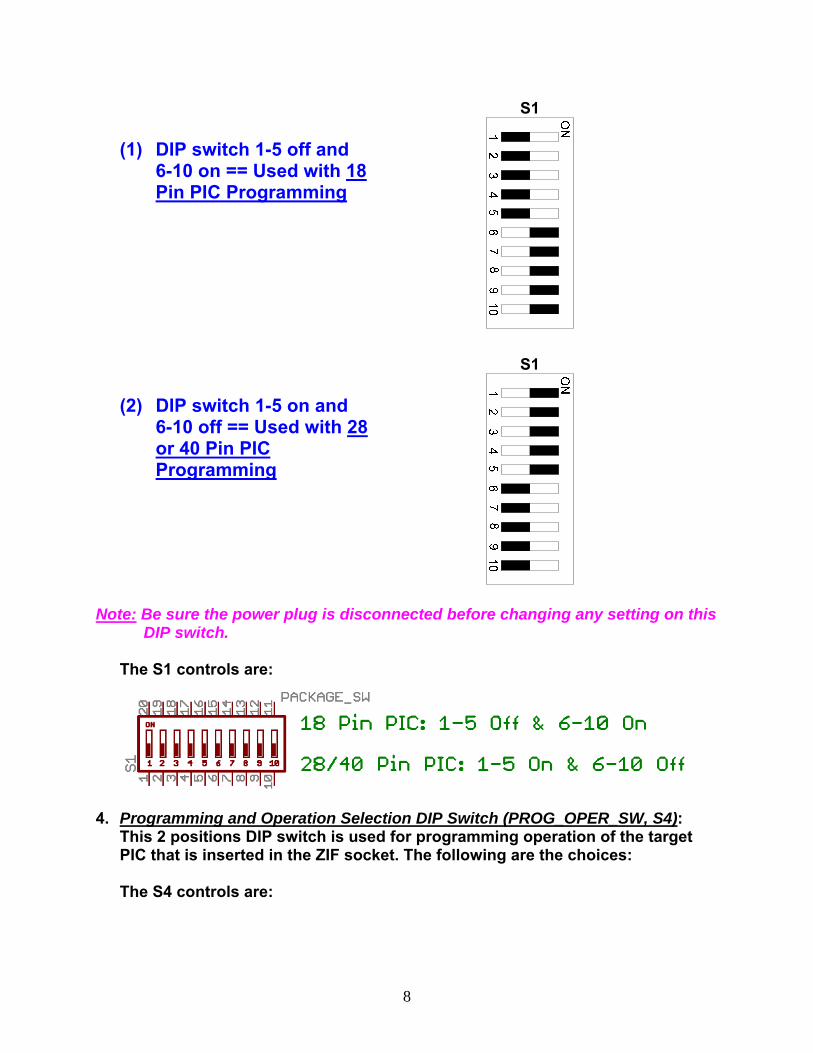
(1) DIP switch 1-5 off and 6-10 on == Used with 18 Pin PIC
S1
3
(2) DIP switch 1-5 on and 6-10 off == Used with 28 or 40 Pin PIC
S1
3. Set the S4 switch properly for target MCU in programming/re-programming operation mode, see S4 switch on Page # 6. (1) SW1 off & SW2 on == Use with 18 Pin PIC Programming
ON
12
PROG_ OPER_SW
S4
(2) SW1 on & SW2 off == Use with 28 or 40 Pin PIC Programming
ON
12
PROG_ OPER_SW
S4
4. Connect USB cable to USB connector X1. 5. Connect the power to J1 power jack. 6. Run PICKT2 or MPLAB software

4
7. The software should recognize the target MCU in the 40Pin ZIF socket. 8. From here you can Import the .HEX file then click Write to program the MCU. Normal Operation: 1. Set S1 and S4 on/off for normal/evaluation operation as following: SW1 on & SW2 on == Use with all 18, 28, or 40 Pin PIC Normal Operations
S1
ON
12
PROG_ OPER_SW
S4
2. Simple press the S2 (for 18 pin PIC) or S3 (for 28 or 40 pin PIC) reset switch, the MCU should boot and running the loaded source code (your .HEX file). Re-programming: 1. Leave S1 package selection switches unchanged and set S4 for different PIC programming settings as:
(1) SW1 off & SW2 on == Use with 18 Pin PIC Programming (2) SW1 on & SW2 off == Use with 28 or 40 Pin PIC Programming
2. Under PICKIT2 “Tools” manual, select “Check Communication”. This should stop the operation mode of the MCU and force it in programming mode. The software should recognize the target MCU in the ZIF socket. 3. If is not successful, press and hold the RESET switch (S2 for 18 Pin PIC or S3 for 28 or 40 Pin PIC) do it again, then the PICKIT2 should recognize the target MCU. 4. If the target MCU still can NOT be recognized, check/do the following: (1) Make sure your application interfaces are not pulled the RB6 and RB7 I/O pins down. (2) If they are, then your choices are (a) Press and hold the RESET switch (S2 for 18 Pin PIC or S3 for 28 or 40 Pin PIC), then click the “Check Communication” make sure the target MCU is recognized by the software, the re-program the MCU in following step #5, after it is done, then power down reconnect the RB6 and RB7 interfaces, then power up. The system should run with your new .HEX file, ignore a signal if it says “Verification Failed”. (b) Power down the system, disconnect the RB6 and RB7 interfaces, power up then click the “Check Communication” make sure the target MCU is recognized by the software, the re-program the MCU in following step #5,
5
after it is done, then power down reconnect the RB6 and RB interfaces, then power up. The system should run with your new .HEX file, ignore a signal if it says “Verification Failed”. (c) Power down the system, disconnect the OSC1 and OSC2 resonator interface between SV4 and MCU oscillator pins, power up the system, then click the “Check Communication” make sure the target MCU is recognized by the software, the re-program the MCU in following step #5, after it is done, then power down reconnect the OSC1 and OSC2 interfaces, then power up. The system should run with your new .HEX file, ignore a signal if it says “Verification Failed”. 5. Press and hold the RESET switch (S2 for 18 Pin PIC or S3 for 28 or 40 Pin PIC), under the main manual “File”, select “Import Hex”, choose the proper .HEX file then click on “Write” to re-program the target MCU. At this point you may encounter a verification fail, but the .HEX should be already programmed and the MCU should start running with your new code. Ignore a signal if it says “Verification Failed”.

6
Hardware Operation The PCB layout of all the electronic components is presented as following:
7
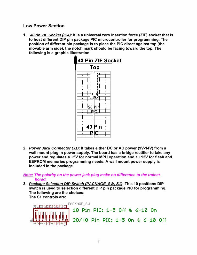
Low Power Section 1. 40Pin ZIF Socket (IC4): It is a universal zero insertion force (ZIF) socket that is
to host different DIP pin package PIC microcontroller for programming. The position of different pin package is to place the PIC direct against top (the movable arm side), the notch mark should be facing toward the top. The following is a graphic illustration:
2. Power Jack Connector (J1): It takes either DC or AC power (9V-14V) from a wall mount plug in power supply. The board has a bridge rectifier to take any power and regulates a +5V for normal MPU operation and a +12V for flash and EEPROM memories programming needs. A wall mount power supply is included in the package.
Note: The polarity on the power jack plug make no difference to the trainer borad. 3. Package Selection DIP Switch (PACKAGE_SW, S1): This 10 positions DIP
switch is used to selection different DIP pin package PIC for programming. The following are the choices:
The S1 controls are:
8
(1) DIP switch 1-5 off and
6-10 on == Used with 18 Pin PIC Programming
S1
(2) DIP switch 1-5 on and 6-10 off == Used with 28 or 40 Pin PIC Programming
S1
Note: Be sure the power plug is disconnected before changing any setting on this DIP switch. The S1 controls are:
4. Programming and Operation Selection DIP Switch (PROG_OPER_SW, S4):
This 2 positions DIP switch is used for programming operation of the target PIC that is inserted in the ZIF socket. The following are the choices:
The S4 controls are:

9
(1) SW1 off & SW2 on == Use with 18 Pin PIC Programming
ON
12
PROG_ OPER_SW
S4
(2) SW1 on & SW2 off == Use with 28 or 40 Pin PIC Programming
ON
12
PROG_ OPER_SW
S4
Normal Operation: Set S1 and S4 on/off as following:
S1
ON
12
PROG_ OPER_SW
S4
Note: The power should be disconnected before changing any of the switches.

10
5. RESET Switch or 18 Pin PIC (S2): This the MCLR pin connection to the 18 pin PIC for any system RESET needs. The circuit is configured as:
6. RESET Switch or 28 or 40 Pin PIC (S3): This the MCLR pin connection to the 18 pin PIC for any system RESET needs. The circuit is configured as:
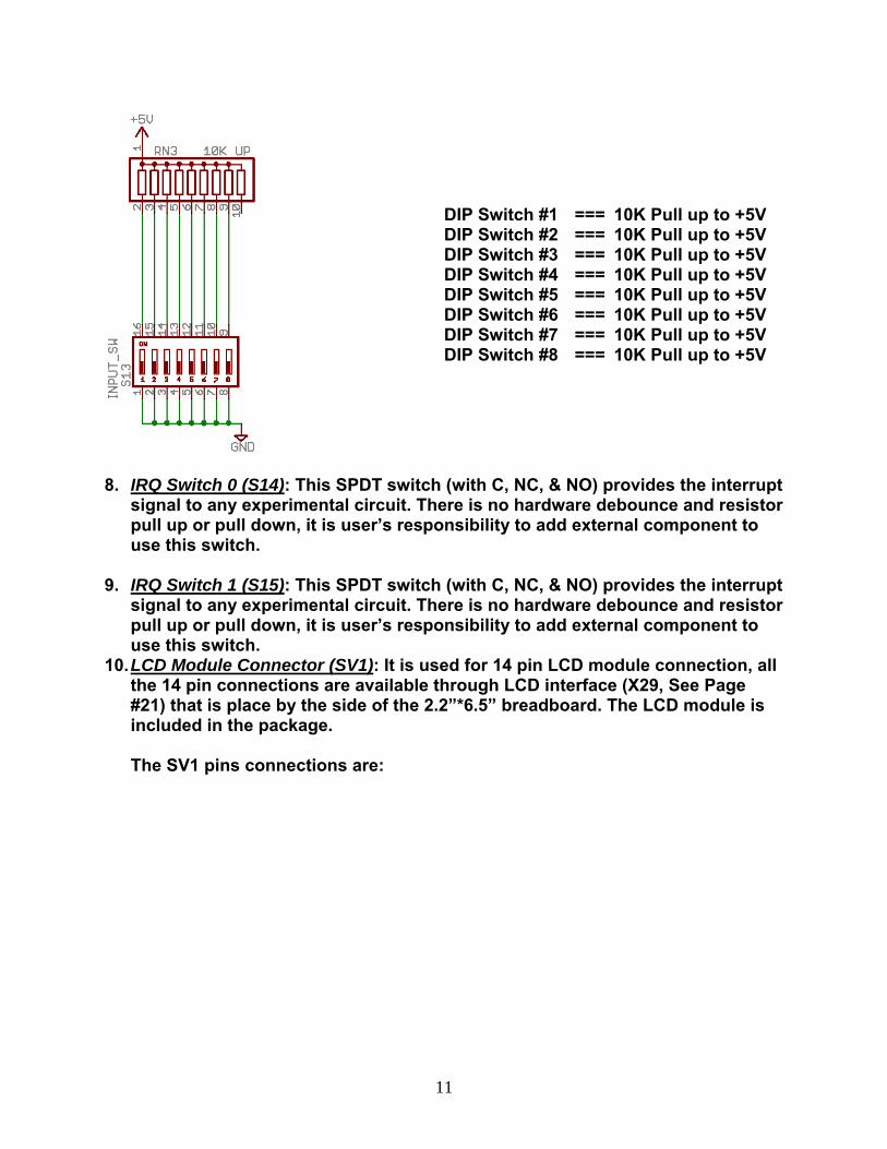
7. 8 Positions DIP Digital Input Switch (S13): This provides 8 bits input to any
experimental circuit. The S13 pin connections are:
11
DIP Switch #1 === 10K Pull up to +5V DIP Switch #2 === 10K Pull up to +5V DIP Switch #3 === 10K Pull up to +5V DIP Switch #4 === 10K Pull up to +5V DIP Switch #5 === 10K Pull up to +5V DIP Switch #6 === 10K Pull up to +5V DIP Switch #7 === 10K Pull up to +5V DIP Switch #8 === 10K Pull up to +5V
8. IRQ Switch 0 (S14): This SPDT switch (with C, NC, & NO) provides the interrupt
signal to any experimental circuit. There is no hardware debounce and resistor pull up or pull down, it is user’s responsibility to add external component to use this switch.
9. IRQ Switch 1 (S15): This SPDT switch (with C, NC, & NO) provides the interrupt
signal to any experimental circuit. There is no hardware debounce and resistor pull up or pull down, it is user’s responsibility to add external component to use this switch.
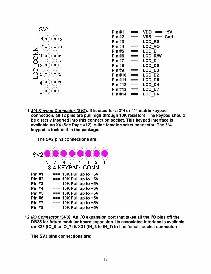
10. LCD Module Connector (SV1): It is used for 14 pin LCD module connection, all the 14 pin connections are available through LCD interface (X29, See Page #21) that is place by the side of the 2.2”*6.5” breadboard. The LCD module is included in the package.
The SV1 pins connections are:
12
Pin #1 === VDD === +5V Pin #2 === VSS === Gnd Pin #3 === LCD_RS Pin #4 === LCD_VO Pin #5 === LCD_E Pin #6 === LCD_R/W Pin #7 === LCD_D1 Pin #8 === LCD_D0 Pin #9 === LCD_D3 Pin #10 === LCD_D2 Pin #11 === LCD_D5 Pin #12 === LCD_D4 Pin #13 === LCD_D7 Pin #14 === LCD_D6
11. 3*4 Keypad Connector (SV2): It is used for a 3*4 or 4*4 matrix keypad connection, all 12 pins are pull high through 10K resistors. The keypad should be directly inserted into this connection socket. This keypad interface is available on X4 (See Page #12) in-line female socket connector. The 3*4 keypad is included in the package.
The SV2 pins connections are:
Pin #1 === 10K Pull up to +5V Pin #2 === 10K Pull up to +5V Pin #3 === 10K Pull up to +5V Pin #4 === 10K Pull up to +5V Pin #5 === 10K Pull up to +5V Pin #6 === 10K Pull up to +5V Pin #7 === 10K Pull up to +5V Pin #8 === 10K Pull up to +5V 12. I/O Connector (SV3): An I/O expansion port that takes all the I/O pins off the
DB25 for future modular board expansion. Its associated interface is available on X38 (IO_0 to IO_7) & X31 (IN_3 to IN_7) in-line female socket connectors.
The SV3 pins connections are:

13
Pin #1 === IO_0 Pin #2 === IO_1 Pin #3 === IO_2 Pin #4 === IO_3 Pin #5 === IO_4 Pin #6 === IO_5 Pin #7 === IO_6
Pin #8 === IO_7 Pin #9 === IN_3 Pin #10 === IN_5 Pin #11 === IN_6 Pin #12 === IN_7 Pin #13 === Gnd Pin #14 === +5V
13. Resonator Interface Connector (SV4): This is an interface for those MCUs (PIC16F84A, PIC16F877A) that need external clock signal to be built with experimental circuit on the 2.2”*6.5” breadboard. The center Gnd pin already wired to the system Gnd trace. The SV4 pins connections are:
Pin #1 === OSC1 === Resonator Pin 1 Pin #2 === Gnd === Resonator Center Pin Pin #3 === OSC2 === Resonator Pin 2
14. MRF24J40MA 2.4 GHz Module Sockets (SV5 & SV6): This a combination of SV5 & SV6 sockets for MRF24J40MA module connection. There is only one orientation of the module that is its antenna has to point out of the PIC Trainer board. The available interface connector is on X36 (See Page #24) This is an actual picture of this MRF24JMA, 2.4 GHz module and its associated

14
interface pins:
The associated circuit is:
15. PIC18F2550 on a 18 Pin Narrow Socket (IC1): This is a resident PIC that is used for communication to a PC via an USB port. It is supposed to be on the socket all the time. Do NOT remove this PIC for any other purpose.
16. Red LED (LED2): It is an indication of the present of the power source. Any
time the wall mount power plug into the power jack, this RED LED will light. 17. Yellow LED (LED1): It is an indication of the USB communication. When it
flashes that indicates the communications processes are either in identifying the type of the PIC, programming a HEX file to the PIC, reading the flash/EEPROM off the PIC, verifying the content of the flash/EEPROM of the PIC, or erasing the content of the PIC.
18. LM7805 Regulator (IC2): This is a +5V power regulator and it can provide +5V
power up to 1A. If the max 1A power is need constantly, a heat sink should be mounted to this TO222 package.
19. LM7812 Regulator (IC3): This is a +12V power regulator and it can provide
+12V power up to 1A. If the max 1A power is need constantly, a heat sink should be mounted to this TO222 package.
Note: Any operation should not cause these LM7805& LM7812 to be hot. If the
15
temperature is hot at these devices, the power jack should be disconnecting immediately and check for any short circuit. During the normal operation this LM7805 & LM7812 should only be warm and touchable by a finger. 20. USB Connector (X1): It is an USB type B female receptacle connector that is
used for regular USB communication to a PC. An USB cable with Type A-B connector is included in the package.
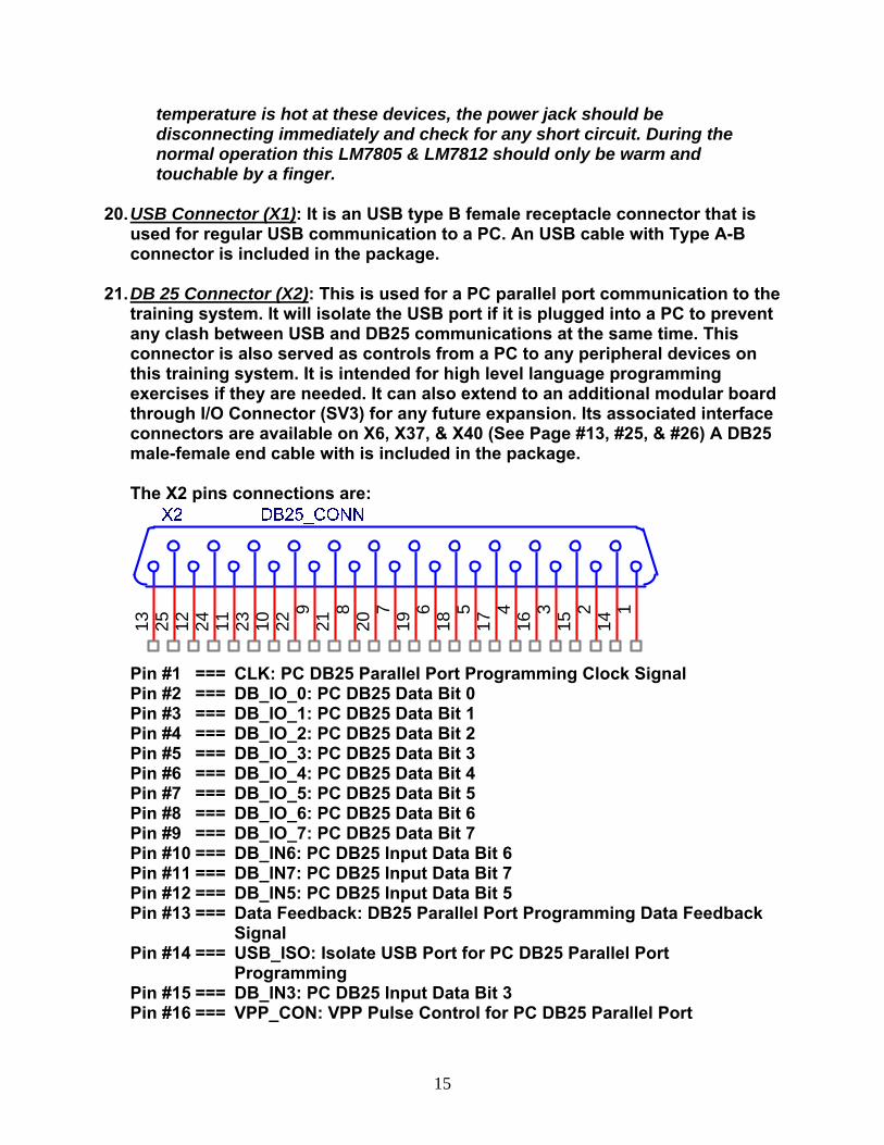
21. DB 25 Connector (X2): This is used for a PC parallel port communication to the
training system. It will isolate the USB port if it is plugged into a PC to prevent any clash between USB and DB25 communications at the same time. This connector is also served as controls from a PC to any peripheral devices on this training system. It is intended for high level language programming exercises if they are needed. It can also extend to an additional modular board through I/O Connector (SV3) for any future expansion. Its associated interface connectors are available on X6, X37, & X40 (See Page #13, #25, & #26) A DB25 male-female end cable with is included in the package.
The X2 pins connections are:
13 25 12 24 11 23 10 229
218
207
196
185
174
163
152
141
Pin #1 === CLK: PC DB25 Parallel Port Programming Clock Signal Pin #2 === DB_IO_0: PC DB25 Data Bit 0 Pin #3 === DB_IO_1: PC DB25 Data Bit 1 Pin #4 === DB_IO_2: PC DB25 Data Bit 2 Pin #5 === DB_IO_3: PC DB25 Data Bit 3 Pin #6 === DB_IO_4: PC DB25 Data Bit 4 Pin #7 === DB_IO_5: PC DB25 Data Bit 5 Pin #8 === DB_IO_6: PC DB25 Data Bit 6 Pin #9 === DB_IO_7: PC DB25 Data Bit 7 Pin #10 === DB_IN6: PC DB25 Input Data Bit 6 Pin #11 === DB_IN7: PC DB25 Input Data Bit 7 Pin #12 === DB_IN5: PC DB25 Input Data Bit 5 Pin #13 === Data Feedback: DB25 Parallel Port Programming Data Feedback Signal Pin #14 === USB_ISO: Isolate USB Port for PC DB25 Parallel Port Programming Pin #15 === DB_IN3: PC DB25 Input Data Bit 3 Pin #16 === VPP_CON: VPP Pulse Control for PC DB25 Parallel Port
16
Programming Pin #17 === DAT: PC DB25 Parallel Port Programming Data Signal Pin #18 – Pin#25: Gnd Its associated IN interfaces are available on X6 (DB_IO_0 to DB_IO_7) & X40
(DB_IN3 to DB_IN7) and Buffered OUT interfaces are on X37 (BUF_IO_0 to BUF_IO_7) in-line female socket connectors.
22. USB Connector (X3): It is another USB type B female receptacle connector that
is used for experimental USB communication to a PC or any other device. The interface connection of +D, -D, Gnd are already set up to the USB port pins on a PIC18F2550 that should be inserted in the ZIF socket.
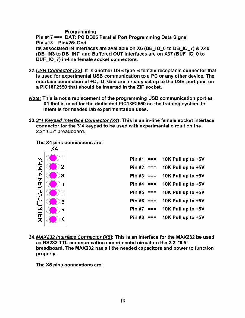
Note: This is not a replacement of the programming USB communication port as X1 that is used for the dedicated PIC18F2550 on the training system. Its intent is for needed lab experimentation uses. 23. 3*4 Keypad Interface Connector (X4): This is an in-line female socket interface
connector for the 3*4 keypad to be used with experimental circuit on the 2.2”*6.5” breadboard.
The X4 pins connections are:
Pin #1 === 10K Pull up to +5V
Pin #2 === 10K Pull up to +5V
Pin #3 === 10K Pull up to +5V
Pin #4 === 10K Pull up to +5V
Pin #5 === 10K Pull up to +5V
Pin #6 === 10K Pull up to +5V
Pin #7 === 10K Pull up to +5V
Pin #8 === 10K Pull up to +5V
24. MAX232 Interface Connector (X5): This is an interface for the MAX232 be used
as RS232-TTL communication experimental circuit on the 2.2”*6.5” breadboard. The MAX232 has all the needed capacitors and power to function properly.
The X5 pins connections are:
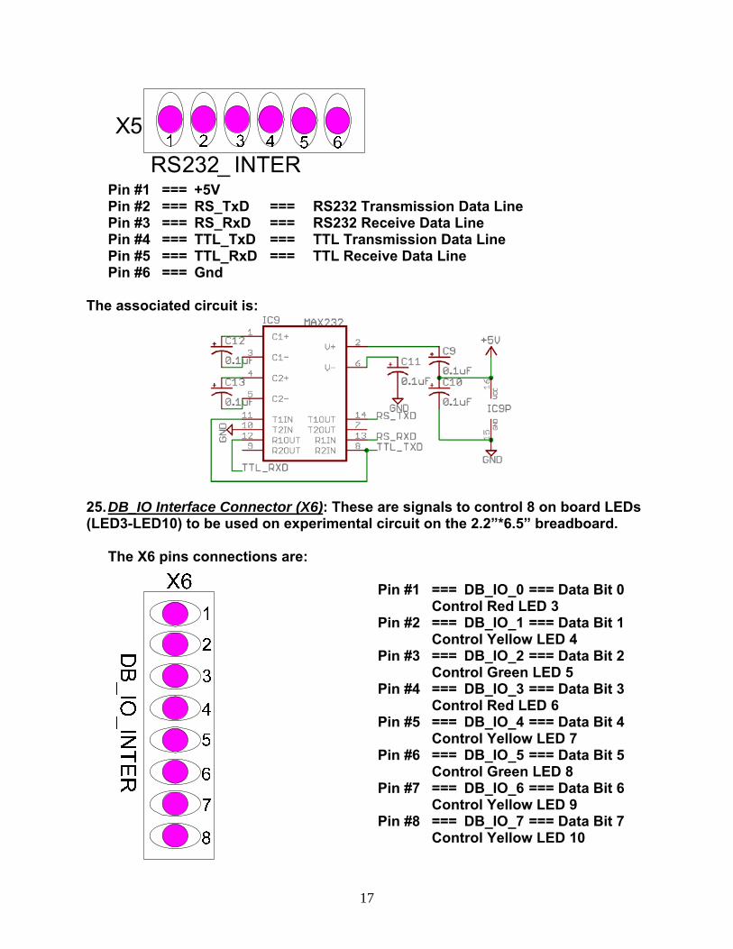
17
Pin #1 === +5V Pin #2 === RS_TxD === RS232 Transmission Data Line Pin #3 === RS_RxD === RS232 Receive Data Line Pin #4 === TTL_TxD === TTL Transmission Data Line Pin #5 === TTL_RxD === TTL Receive Data Line Pin #6 === Gnd The associated circuit is:
25. DB_IO Interface Connector (X6): These are signals to control 8 on board LEDs (LED3-LED10) to be used on experimental circuit on the 2.2”*6.5” breadboard. The X6 pins connections are:
Pin #1 === DB_IO_0 === Data Bit 0 Control Red LED 3 Pin #2 === DB_IO_1 === Data Bit 1 Control Yellow LED 4 Pin #3 === DB_IO_2 === Data Bit 2 Control Green LED 5 Pin #4 === DB_IO_3 === Data Bit 3 Control Red LED 6 Pin #5 === DB_IO_4 === Data Bit 4 Control Yellow LED 7 Pin #6 === DB_IO_5 === Data Bit 5 Control Green LED 8 Pin #7 === DB_IO_6 === Data Bit 6 Control Yellow LED 9 Pin #8 === DB_IO_7 === Data Bit 7 Control Yellow LED 10

18
It associated circuit is:
……. 26. OPAMP Interface Connector (X7): This is an interface for MCP6024 that is a
general Operational Amplifier to be built with experimental circuit on the 2.2”*6.5” breadboard. This MCP6014 has four OPAmps in one package for any conditional circuit to be used.
The X7 pins connections are:
Pin #1 === OPA0_OUT === OPAmp #0 Output Pin #2 === OPA0- === OPAmp #0 - Input Pin #3 === OPA0+ === OPAmp #0+ Input Pin #4 === OPA1+ === OPAmp #1 + Input Pin #5 === OPA1- === OPAmp #1 - Input Pin #6 === OPA1_OUT === OPAmp #1 Output Pin #7 === OPA2+ === OPAmp #2 + Input Pin #8 === OPA2- === OPAmp #2 - Input Pin #9 === OPA2_OUT === OPAmp #2 Output Pin #10 === OPA3+ === OPAmp #3 + Input Pin #11 === OPA3- === OPAmp #3 - Input Pin #12 === OPA3_OUT === OPAmp #3 Output
19
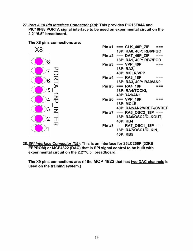
27. Port A 18 Pin Interface Connector (X8): This provides PIC16F84A and PIC16F88 PORTA signal interface to be used on experimental circuit on the 2.2”*6.5” breadboard.
The X8 pins connections are:
Pin #1 === CLK_40P_ZIF === 18P: RA0, 40P: RB6/PGC Pin #2 === DAT_40P_ZIF === 18P: RA1, 40P: RB7/PGD Pin #3 === VPP_40P === 18P: RA2, 40P: MCLR/VPP Pin #4 === RA3_18P === 18P: RA3, 40P: RA0/AN0 Pin #5 === RA4_18P === 18P: RA4/TOCKI, 40P:RA1/AN1 Pin #6 === VPP_18P === 18P: MCLR, 40P: RA2/AN2/VREF-/CVREF Pin #7 === RA6_OSC2_18P === 18P: RA6/OSC2/CLKOUT, 40P: RB4 Pin #8 === RA7_OSC1_18P === 18P: RA7/OSC1/CLKIN, 40P: RB5
28. SPI Interface Connector (X9): This is an interface for 25LC256P (32KB
EEPROM) or MCP4822 (DAC) that is SPI signal control to be built with experimental circuit on the 2.2”*6.5” breadboard.
The X9 pins connections are: (If the MCP 4822 that has two DAC channels is
used on the training system.)
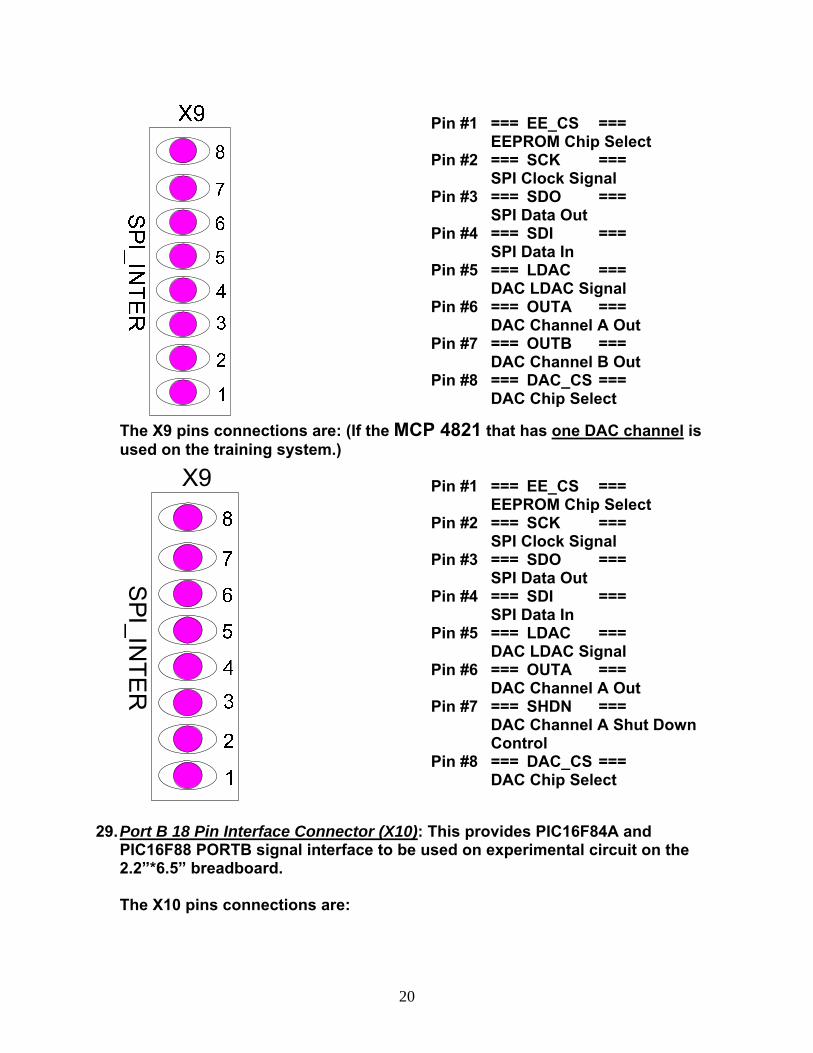
20
Pin #1 === EE_CS === EEPROM Chip Select Pin #2 === SCK === SPI Clock Signal Pin #3 === SDO === SPI Data Out Pin #4 === SDI === SPI Data In Pin #5 === LDAC === DAC LDAC Signal Pin #6 === OUTA === DAC Channel A Out Pin #7 === OUTB === DAC Channel B Out Pin #8 === DAC_CS === DAC Chip Select
The X9 pins connections are: (If the MCP 4821 that has one DAC channel is used on the training system.)
Pin #1 === EE_CS === EEPROM Chip Select Pin #2 === SCK === SPI Clock Signal Pin #3 === SDO === SPI Data Out Pin #4 === SDI === SPI Data In Pin #5 === LDAC === DAC LDAC Signal Pin #6 === OUTA === DAC Channel A Out Pin #7 === SHDN === DAC Channel A Shut Down Control Pin #8 === DAC_CS === DAC Chip Select
29. Port B 18 Pin Interface Connector (X10): This provides PIC16F84A and
PIC16F88 PORTB signal interface to be used on experimental circuit on the 2.2”*6.5” breadboard.
The X10 pins connections are:
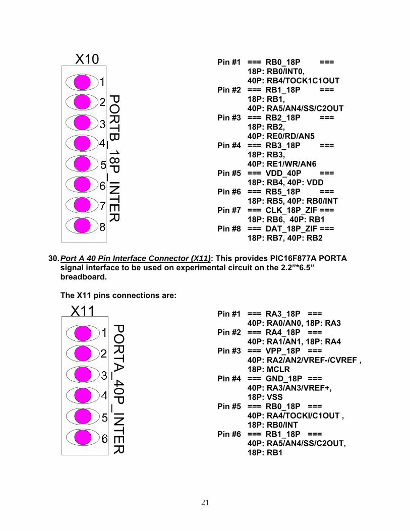
21
Pin #1 === RB0_18P === 18P: RB0/INT0, 40P: RB4/TOCK1C1OUT Pin #2 === RB1_18P === 18P: RB1, 40P: RA5/AN4/SS/C2OUT Pin #3 === RB2_18P === 18P: RB2, 40P: RE0/RD/AN5 Pin #4 === RB3_18P === 18P: RB3, 40P: RE1/WR/AN6 Pin #5 === VDD_40P === 18P: RB4, 40P: VDD Pin #6 === RB5_18P === 18P: RB5, 40P: RB0/INT Pin #7 === CLK_18P_ZIF === 18P: RB6, 40P: RB1 Pin #8 === DAT_18P_ZIF === 18P: RB7, 40P: RB2
30. Port A 40 Pin Interface Connector (X11): This provides PIC16F877A PORTA
signal interface to be used on experimental circuit on the 2.2”*6.5” breadboard.
The X11 pins connections are:
Pin #1 === RA3_18P === 40P: RA0/AN0, 18P: RA3 Pin #2 === RA4_18P === 40P: RA1/AN1, 18P: RA4 Pin #3 === VPP_18P === 40P: RA2/AN2/VREF-/CVREF , 18P: MCLR Pin #4 === GND_18P === 40P: RA3/AN3/VREF+, 18P: VSS Pin #5 === RB0_18P === 40P: RA4/TOCKI/C1OUT , 18P: RB0/INT Pin #6 === RB1_18P === 40P: RA5/AN4/SS/C2OUT, 18P: RB1
22
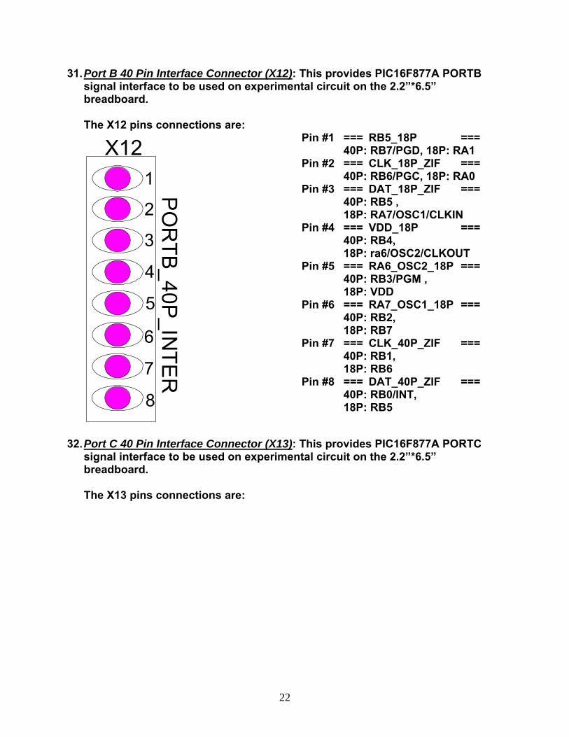
31. Port B 40 Pin Interface Connector (X12): This provides PIC16F877A PORTB signal interface to be used on experimental circuit on the 2.2”*6.5” breadboard.
The X12 pins connections are:
Pin #1 === RB5_18P === 40P: RB7/PGD, 18P: RA1 Pin #2 === CLK_18P_ZIF === 40P: RB6/PGC, 18P: RA0 Pin #3 === DAT_18P_ZIF === 40P: RB5 , 18P: RA7/OSC1/CLKIN Pin #4 === VDD_18P === 40P: RB4, 18P: ra6/OSC2/CLKOUT Pin #5 === RA6_OSC2_18P === 40P: RB3/PGM , 18P: VDD Pin #6 === RA7_OSC1_18P === 40P: RB2, 18P: RB7 Pin #7 === CLK_40P_ZIF === 40P: RB1, 18P: RB6 Pin #8 === DAT_40P_ZIF === 40P: RB0/INT, 18P: RB5
32. Port C 40 Pin Interface Connector (X13): This provides PIC16F877A PORTC
signal interface to be used on experimental circuit on the 2.2”*6.5” breadboard.
The X13 pins connections are:

23
Pin #1 === RC0_40P === 40P: RC0/T1OSO/T1CKI Pin #2 === RC1_40P === 40P: RC1/T1OSI/CCP2 Pin #3 === RC2_40P === 40P: RC2/CCP1 Pin #4 === RC3_40P === 40P: RC3/SCK/SCL Pin #5 === RC4_40P === 40P: RC4/SDI/SDA Pin #6 === RC5_40P === 40P: RC5/SDO Pin #7 === RC6_40P === 40P: RC6/TX/CK Pin #8 === RC7_40P === 40P: RC7/RX/DT
33. Port D 40 Pin Interface Connector (X14): This provides PIC16F877A PORTD
signal interface to be used on experimental circuit on the 2.2”*6.5” breadboard.
The X14 pins connections are:
PO
RT
D_4
0P
_INT
ER
Pin #1 === RD0_40P === 40P: RD0/PSP0 Pin #2 === RD1_40P === 40P: RD1/PSP1 Pin #3 === RD2_40P === 40P: RD2PSP2 Pin #4 === RD3_40P === 40P: RD3/PSP3 Pin #5 === USB_D- === 40P: RD4/PSP4, 28P: USB D- Pin #6 === USB_D+ === 40P: RD5/PSP5, 28P: USB D+ Pin #7 === RD6_40P === 40P: RD6/PSP6 Pin #8 === RD7_40P === 40P: RD7/PSP7
34. Port E 40 Pin Interface Connector (X15): This provides PIC16F877A PORTE
signal interface to be used on experimental circuit on the 2.2”*6.5” breadboard.

24
The X15 pins connections are:
Pin #1 === RB2_18P === 40P: RE0/RD/AN5 Pin #2 === RB3_18P === 40P: RE1/WR/AN6 Pin #3 === RE2_40P === 40P: RE2/CS/AN7 Pin #4 === OSC1_40P === 40P: OS1I/CLKI Pin #5 === OSC2_40P === 40P: OSC2/CLKO 35. DC Power Source (X27): This +5V power source that is on two terminal block
posts (one for +5V the other for Gnd) for providing power source to any experimental circuit on the 2.2”*6.5” breadboard.
The X27 pins connections are:
Pin 1 & Pin 2 === +5V Pin 3 & Pin 4 === Gnd
36. Debounced Switches Connector (X28): This is an interface debounced SPDT switches of S5-S12 to be used with experimental circuit on the 2.2”*6.5” breadboard.
The X28 pins connections are:
Pin #1 == DB_SW0 == Controlled by S5 Pin #2 == DB_SW1 == Controlled by S6 Pin #3 == DB_SW2 == Controlled by S7 Pin #4 == DB_SW3 == Controlled by S8 Pin #5 == DB_SW4 == Controlled by S9 Pin #6 == DB_SW5 == Controlled by S10 Pin #7 == DB_SW6 == Controlled by S11 Pin #8 == DB_SW7 == Controlled by S12

25
The associated circuit of these 8 hardware debounced switches are:
37. LCD Interface Connector (X29): This is an interface for the LCD to be used with
experimental circuit on the 2.2”*6.5” breadboard. The X29 pins connections are:
Pin #1 === LCD_D0 (LCD Pin #7)
Pin #2 === LCD_D1 (LCD Pin #8)
Pin #3 === LCD_D2 (LCD Pin #9)
Pin #4 === LCD_D3 (LCD Pin #10)
Pin #5 === LCD_D4 (LCD Pin #11)
Pin #6 === LCD_D5 (LCD Pin #12)
Pin #7 === LCD_D6 (LCD Pin #13)
Pin #8 === LCD_D7 (LCD Pin #14)
Pin #9 === LCD_RS (LCD Pin #4)
Pin #10 === LCD_E (LCD Pin #6)
Pin #11 === LCD_R/W (LCD Pin #5)
Pin #12 === LCD_VO (LCD Pin #3) Note: LCD Pin #1, Vss, is Grounded and LCD Pin #2, Vdd is Powered by +5V on the board.
38. Potentiometer 1 Interface Connector (X30): These are signals from 10K Ω Trim
Potentiometer 1 connector for any adjustable voltage signal that can be interfaced to experimental circuit on the 2.2”*6.5” breadboard.

26
The X30 pins connections are:
Pin #1 === One end of the 10K Ω Pot Pin #2 === Center wiper of the Pot 1 Pin #3 === The other end of the 10K Ω Pot
39. IN Interface Connector (X31): These are input signals going to DB25 input pins that can be interfaced to experimental circuit on the 2.2”*6.5” breadboard.
The X31 pins connections are:
Pin #1 === +5V
Pin #2 === IN_3
Pin #3 === IN_5
Pin #4 === IN_6
Pin #5 === IN_7
Pin #6 === Gnd
The associate circuits of these input pins are presented in item #48. 40. 8 Positions DIP Digital Input Switch Interface Connector(X32): This is an interface for the 8 bit DIP switch to be used as inputs for experimental circuit on the 2.2”*6.5” breadboard. The X32 pins connections are:
Pin #1 === DIP Switch #1 Down = Gnd/Lo, Up = +5V/Hi Pin #2 === DIP Switch #2 Down = Gnd/Lo, Up = +5V/Hi Pin #3 === DIP Switch #3 Down = Gnd/Lo, Up = +5V/Hi

27
Pin #4 === DIP Switch #4 Down = Gnd/Lo, Up = +5V/Hi Pin #5 === DIP Switch #5 Down = Gnd/Lo, Up = +5V/Hi Pin #6 === DIP Switch #6 Down = Gnd/Lo, Up = +5V/Hi Pin #7 === DIP Switch #7 Down = Gnd/Lo, Up = +5V/Hi Pin #8 === DIP Switch #8 Down = Gnd/Lo, Up = +5V/Hi 41. 7 Segment Interface Connector (X33): This is an interface for data signal to all
4 of the 7 segment display experimental circuit on the 2.2”*6.5” breadboard. To activate one of the four 7 segment, a proper activation signal on the driver connector should be high.
The X33 pins connections are:
Pin #1 === Segment a thru 220Ω Current Limit, Output Lo to Turn on
Pin #2 === Segment b through 220Ω Current Limit, Output Lo to Turn on
Pin #3 === Segment c through 220Ω Current Limit, Output Lo to Turn on
Pin #4 === Segment d through 220Ω Current Limit, Output Lo to Turn on
Pin #5 === Segment e through 220Ω Current Limit, Output Lo to Turn on
Pin #6 === Segment f through 220Ω Current Limit, Output Lo to Turn on
Pin #7 === Segment g through 220Ω Current Limit, Output Lo to Turn on
Pin #8 === Segment dp through 220Ω Current Limit, Output Lo to Turn on
42. 7 Segment Driver Interface Connector (X34): This is a driver signal interface to
activate one of the four 7 segment display experimental circuit on the 2.2”*6.5” breadboard.
The X34 pins connections are:

28
Pin #1 === Segment #0 On/Off Control, Output Lo to Turn on Pin #2 === Segment #1 On/Off Control, Output Lo to Turn on Pin #3 === Segment #2 On/Off Control, Output Lo to Turn on Pin #4 === Segment #3 On/Off Control, Output Lo to Turn on
43. IRQ Switch 0 Interface Connector (X35): This is an interface for the SPDT switch to be used as inputs for interrupt experimental circuit on the 2.2”*6.5” breadboard. The first 3 connections belong to IRQ Switch 0.
44. IRQ Switch 1 Interface Connector (X35): This is an interface for the SPDT
switch to be used as inputs for interrupt experimental circuit on the 2.2”*6.5” breadboard. The second 3 connections belong to IRQ Switch 1.
The X35 pins connections are:
Pin #1 === IRQ_SW0 C (Common) Pin #2 === IRQ_SW0 NO (Normal Open) Pin #3 === IRQ_SW0 NC (Normal Close) Pin #4 === IRQ_SW1 C (Common) Pin #5 === IRQ_SW1 NO (Normal Open) Pin #6 === IRQ_SW1 NC (Normal Close) 45. 2.4 GHz Module Interface Connector (X36): This is a standard SPI interface for
2.4GHz, MRF24J40MA Module interface for wireless communication on the 2.2”*6.5” breadboard.
The X36 pins connections are:
Pin #1 === RF_RESET Pin #2 === RF_WAKE

29
Pin #3 === RF_INT Pin #4 === SDO Pin #5 === SCK Pin #6 === CLKOUT Pin #7 === RF_CS Pin #8 === SDI The associate circuits of these input/SPI interfaces are presented in item #14. 45. DB_BUF_IO Interface Connector (X37): These are buffered signals from DB25,
DB_IO to any 8 bit IO control interface that can be used on experimental circuit on the 2.2”*6.5” breadboard.
The X37 pins connections are:
Pin #1 === BUF_IO_0 Pin #2 === BUF_IO_1
Pin #3 === BUF_IO_2 Pin #4 === BUF_IO_3 Pin #5 === BUF_IO_4 Pin #6 === BUF_IO_5 Pin #7 === BUF_IO_6 Pin #8 === BUF_IO_7
The associated circuits from DB_IO to BUF_IO signal are:
…… 46. IO Interface Connector (X38): These are signals from DB25, DB_IO to any 8 bit
IO control interface that can be used on experimental circuit on the 2.2”*6.5” breadboard. See Item #45 for relation between DB_IO & BUF_IO.
The X38 pins connections are:
Pin #1 === IO_0 Pin #2 === IO_1

30
Pin #3 === IO_2 Pin #4 === IO_3 Pin #5 === IO_4 Pin #6 === IO_5 Pin #7 === IO_6 Pin #8 === IO_7 47. Potentiometer 2 Interface Connector (X39): These are signals from 10K Ω Trim
Potentiometer 2 connector for any adjustable voltage signal that can be interfaced to experimental circuit on the 2.2”*6.5” breadboard.
The X39 pins connections are:
Pin #1 === One end of the 10K Ω Pot Pin #2 === Center wiper of the Pot 1 Pin #3 === The other end of the 10K Ω Pot
48. Buffered Input Interface Connector (X40): These are buffered input signals that are intended for DB25 input purpose that can be interfaced to experimental circuit on the 2.2”*6.5” breadboard.
The X40 pins connections are:
Pin #1 === DB_IN3 Pin #2 === DB_IN5 Pin #3 === DB_IN6 Pin #4 === DB_IN7 Note: DB_IN7 is inversed
The associated relationship between input and buffered input pins are:
...

31
49. Switches 5-12 (S5, S6, S7, S8, S9, S10, S11, S12): These are 8 hardware debounced SPDT switches to be used in experimental circuit on the 2.2”*6.5” breadboard.
50. LED 23-30 (Green LED23, LED24, LED25, LED26, LED27, LED28, LED29,
LED3): These are indication LEDs for signal the action on the hardware debounced switches 5-12.
51. LED 3-10 (Red LED3, Green LED4, Yellow LED5, Red LED6, Green LED7,
Yellow LED8, Yellow LED9, Yellow LED10): These are indication LEDs for signal output logics on DB_IO_0, DB_IO_1, DB_IO_2, DB_IO_3, DB_IO_4, DB_IO_5, DB_IO_6, DB_IO_7.
52. LED 31-34 (Yellow LED31, Yellow LED32, Yellow LED33, Yellow LED34): These are indication LEDs for input logic signals on IN_3, IN_5, IN_6, & IN_7.

32
High Power Section All the high power components are isolated from the low power side (there is no common ground between the low and high power components) and positioned at right side of the PCB and all the interface connectors are terminal blocks for low gauge wire high current connection flow. The graphic symbols representations are the same as they placed on the PCB. 1. The Power FET 0 Connector (X16): The IRF530 power FET 0 is activated by
IO_0 logic Hi, if it is activated the OUT_0 pin will be connected to OUT_0_GND pin. This will allow high power on/off control to power ground terminal.
The X16 pins connections are:
Pin #1 === VCC === Motor Power Pin #2 === OUT_0 ===
Power FET 0 Drain, Connected to OUT_0_GND If Activated
Pin #3 === OUT_0_GND === Motor Power GND
2. The Power FET 1 Connector (X17): The IRF530 power FET 1 is activated by IO_1 logic Hi, if it is activated the OUT_1 pin will be connected to OUT_1_GND pin. This will allow high power on/off control to power ground terminal. The X17 pins connections are:
Pin #1 === VCC === Motor Power Pin #2 === OUT_1 ===
Power FET 1 Drain, Connected to OUT_1_GND If Activated
Pin #3 === OUT_1_GND === Motor Power GND
3. The Power FET 2 Connector (X18): The IRF530 power FET 2 is activated by IO_2 logic Hi, if it is activated the OUT_2 pin will be connected to OUT_2_GND pin. This will allow high power on/off control to power ground terminal.
The X18 pins connections are:
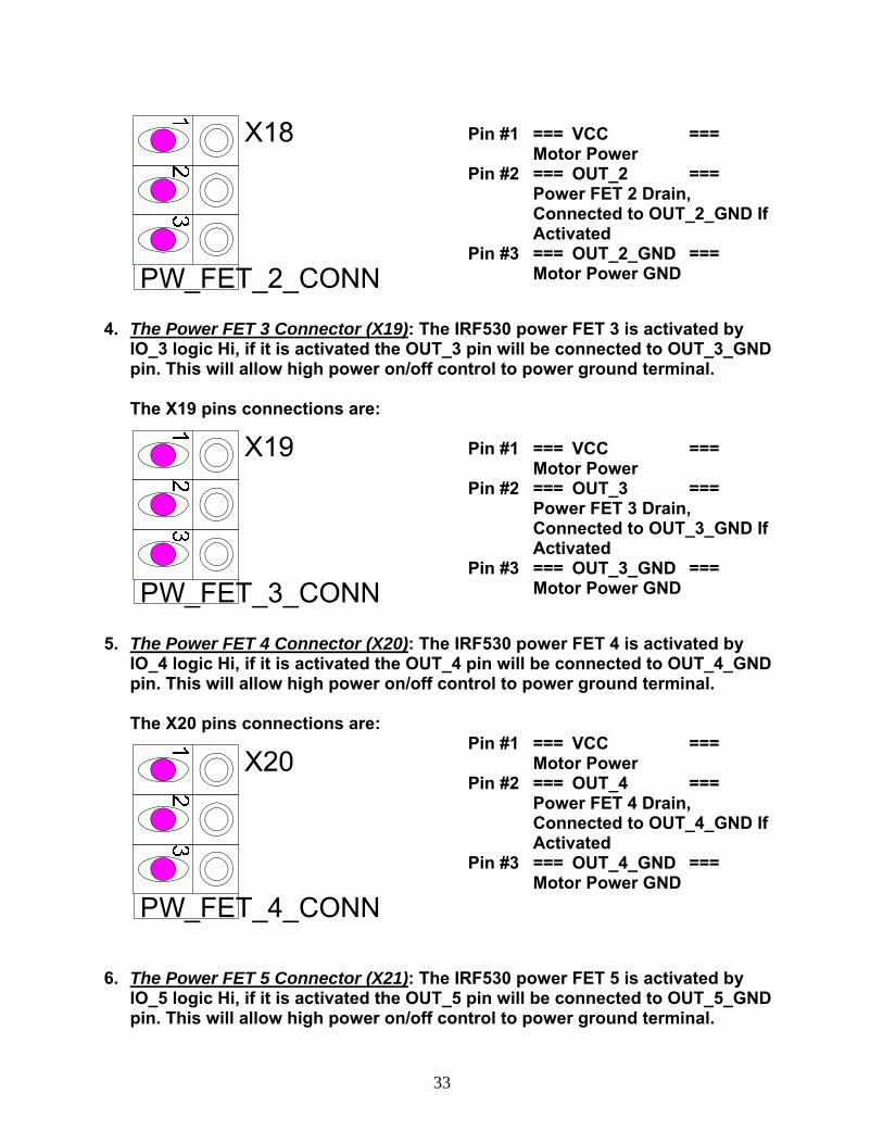
33
Pin #1 === VCC === Motor Power Pin #2 === OUT_2 ===
Power FET 2 Drain, Connected to OUT_2_GND If Activated
Pin #3 === OUT_2_GND === Motor Power GND
4. The Power FET 3 Connector (X19): The IRF530 power FET 3 is activated by
IO_3 logic Hi, if it is activated the OUT_3 pin will be connected to OUT_3_GND pin. This will allow high power on/off control to power ground terminal.
The X19 pins connections are:
Pin #1 === VCC === Motor Power Pin #2 === OUT_3 ===
Power FET 3 Drain, Connected to OUT_3_GND If Activated
Pin #3 === OUT_3_GND === Motor Power GND
5. The Power FET 4 Connector (X20): The IRF530 power FET 4 is activated by
IO_4 logic Hi, if it is activated the OUT_4 pin will be connected to OUT_4_GND pin. This will allow high power on/off control to power ground terminal.
The X20 pins connections are:
Pin #1 === VCC === Motor Power Pin #2 === OUT_4 ===
Power FET 4 Drain, Connected to OUT_4_GND If Activated
Pin #3 === OUT_4_GND === Motor Power GND
6. The Power FET 5 Connector (X21): The IRF530 power FET 5 is activated by IO_5 logic Hi, if it is activated the OUT_5 pin will be connected to OUT_5_GND pin. This will allow high power on/off control to power ground terminal.

34
The X21 pins connections are:
Pin #1 === VCC === Motor Power Pin #2 === OUT_5 ===
Power FET 5 Drain, Connected to OUT_5_GND If Activated
Pin #3 === OUT_5_GND === Motor Power GND
7. The Power FET 6 Connector (X22): The IRF530 power FET 6 is activated by
IO_6 logic Hi, if it is activated the OUT_6 pin will be connected to OUT_6_GND pin. This will allow high power on/off control to power ground terminal.
The X22 pins connections are:
Pin #1 === VCC === Motor Power Pin #2 === OUT_6 ===
Power FET 6 Drain, Connected to OUT_6_GND If Activated
Pin #3 === OUT_6_GND === Motor Power GND
8. The Power FET 7 Connector (X23): The IRF530 power FET 7 is activated by IO_7 logic Hi, if it is activated the OUT_7 pin will be connected to OUT_7_GND pin. This will allow high power on/off control to power ground terminal. The X23 pins connections are:
Pin #1 === VCC === Motor Power Pin #2 === OUT_7 ===
Power FET 7 Drain, Connected to OUT_7_GND If Activated
Pin #3 === OUT_7_GND === Motor Power GND

35
9. The Motor Power/High Power Connector (X24): This is the terminals for high power inputs to be use for motor controls. This ground is the same as system +5V ground. To isolate the power ground, wires should be connected directly to power FET ground.
The X24 pins connections are:
Pin #1 === VCC Pin #2 === GND
10. H-Bridge 1 Connector (X25): This is H-Bridge #1 connector for applications with IRF530 controls on high power Unipolar stepper motor or DC motor directions. The X25 pins connections are:
Pin #1 === HB1_1 Pin #2 === HB1_2
The associate circuit of this X25 connector is:
Note: IRF530/Q3 is activated via IO_0 logic pin 1 in X38 interface connector. IRF530/Q4 is activated via IO_1 logic pin 2 in X38 interface connector. IRF530/Q5 is activated via IO_2 logic pin 3 in X38 interface connector. IRF530/Q6 is activated via IO_3 logic pin 4 in X38 interface connector. All the logic signals are isolated through optical isolator between MCU and motor power signals.

36
Users need to connect proper wires on terminal blocks (X16, X17, X18, & X19) to make the H-Bridge #1, the followings are the suggested connections and their associated circuits stated in item #11.
(1) VCC (motor power, any Pin #1 on X16, X17, X18 or X19) to OUT_0 (Pin #2 on X16) & OUT_1 (Pin #2 on X17)
(2) OUT_0_GND (Pin #3 on X16) & OUT_2 (Pin #2 on X18) & HB1_1 (Pin #1 on X25)
(3) OUT_1_GND (Pin #3 on X17) & OUT_3 (Pin #2 on X19) & HB1_2 (Pin #2 on X25)
(4) OUT_2_GND (Pin #3 on X18) & OUT_3_GND (Pin #3 on X19) to Motor Power GND (Pin #2 on X24)
(5) HB1_1 (Pin #1 on X25) & HB1_2 (Pin #2 on X25) to Motor Terminals. Activate IO_0 and IO_3 to and disable IO_1 and IO_2 to drive DC motor in one direction. Activate I1_0 and IO_2 to and disable IO_0 and IO_3 to drive DC motor in the other direction. Note: In this configuration, never active both IRF530/Q3 (IO_0) & IRF530/Q5 (IO_2) and/or both IRF530/Q4 (IO_1) & IRF530/Q6 (IO_3) at the same time. This will cause a direct short of VCC to GND. 11. The Equivalent H-Bridge (HB1) Circuit with IO and IRF530: The equivalent H-
Bridge 1 circuit connections that described in item #10 are presented as: (Note: the IO_0, IO_1, IO_2, IO_3 are not directly connected (they go through the optical isolator) to the gates of the associate IRFs)
12. LED11/Green & LED12/Yellow: These are current direction flow indicators for H-Bridge #1 control applications. 13. H-Bridge 2 Connector (X26): This is H-Bridge #2 connector for applications with IRF530 controls on high power Unipolar stepper motor or DC motor directions.
37
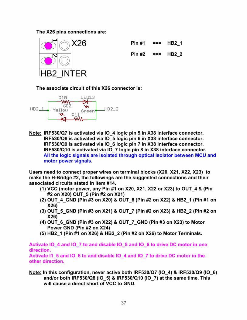
The X26 pins connections are:
12
Pin #1 === HB2_1 Pin #2 === HB2_2
The associate circuit of this X26 connector is:
Note: IRF530/Q7 is activated via IO_4 logic pin 5 in X38 interface connector. IRF530/Q8 is activated via IO_5 logic pin 6 in X38 interface connector. IRF530/Q9 is activated via IO_6 logic pin 7 in X38 interface connector. IRF530/Q10 is activated via IO_7 logic pin 8 in X38 interface connector. All the logic signals are isolated through optical isolator between MCU and motor power signals. Users need to connect proper wires on terminal blocks (X20, X21, X22, X23) to make the H-Bridge #2, the followings are the suggested connections and their associated circuits stated in item #14.
(1) VCC (motor power, any Pin #1 on X20, X21, X22 or X23) to OUT_4 & (Pin #2 on X20) OUT_5 (Pin #2 on X21)
(2) OUT_4_GND (Pin #3 on X20) & OUT_6 (Pin #2 on X22) & HB2_1 (Pin #1 on X26)
(3) OUT_5_GND (Pin #3 on X21) & OUT_7 (Pin #2 on X23) & HB2_2 (Pin #2 on X26)
(4) OUT_6_GND (Pin #3 on X22) & OUT_7_GND (Pin #3 on X23) to Motor Power GND (Pin #2 on X24)
(5) HB2_1 (Pin #1 on X26) & HB2_2 (Pin #2 on X26) to Motor Terminals. Activate IO_4 and IO_7 to and disable IO_5 and IO_6 to drive DC motor in one direction. Activate I1_5 and IO_6 to and disable IO_4 and IO_7 to drive DC motor in the other direction. Note: In this configuration, never active both IRF530/Q7 (IO_4) & IRF530/Q9 (IO_6) and/or both IRF530/Q8 (IO_5) & IRF530/Q10 (IO_7) at the same time. This will cause a direct short of VCC to GND.
38
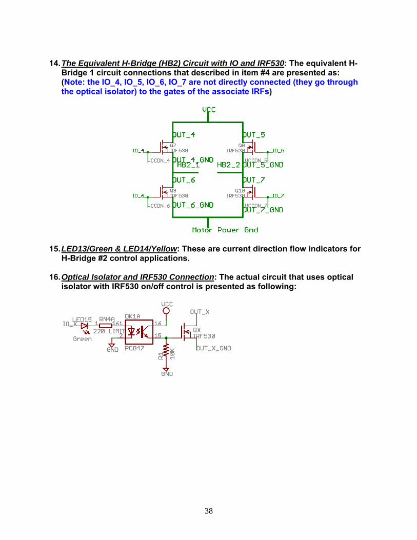
14. The Equivalent H-Bridge (HB2) Circuit with IO and IRF530: The equivalent H-
Bridge 1 circuit connections that described in item #4 are presented as: (Note: the IO_4, IO_5, IO_6, IO_7 are not directly connected (they go through
the optical isolator) to the gates of the associate IRFs)
15. LED13/Green & LED14/Yellow: These are current direction flow indicators for H-Bridge #2 control applications. 16. Optical Isolator and IRF530 Connection: The actual circuit that uses optical
isolator with IRF530 on/off control is presented as following:

39
Software Operations: PICKIT2 PIC Programming Download the PICKIT2 2.40V: This software is available www.microchip.com/pickit2 After the installation and execute the software, you should be able to see a menu screen like this: 1. Device: It is an indication of what type of PIC family member is currently in the
ZIF socket. 2. Configuration: It indicates what configuration word is in your source code
setting. 3. Status Bar: It indicates the communication status. 4. Read: It reads the content of the PIC flash and EEPROM.
40
5. Write: It writes the source code (.HEX file) to the PIC flash memory. 6. Verify: It verifies the content of the PIC with the buffer memory in a PC. 7. Erase: It erase the content of flash and EEPROM memory from the PIC. 8. Blank Check: It checks the content of flash and EEPROM memory for blank. 9. Program Memory: It indicates the flash memory content of the PIC or the PC
buffer memory. 10. EEPROM Memory: It indicates the EEPROM memory content of the PIC or the
PC buffer memory. 11. File Menu - Import Hex: Load the .HEX into the PC buffer memory. This has to
be done before any programming of a PIC can proceed. 12. File Menu - Export Hex: Wire the PC buffer memory to a file on the PC. This
enables you to upload the flash memory content of the PIC to a PC and make it a .HEX file.
13. Device Family Menu: This allows you to choose different PIC family member
for programming purpose. 14. Programmer Menu: This is the same as Read, Write, Verify, Erase, Blank
Check as describe before. 15. Tools Menu– Check Communication: This allows you to check the USB
communication between the programmer board and a PC connection. Note: There are features in the PICKIT2 software that is related to Microchip hardware but not usable in this ODU programmer. NOT every function in the PICKIT2 software is implemented in this programmer hardware design.
41
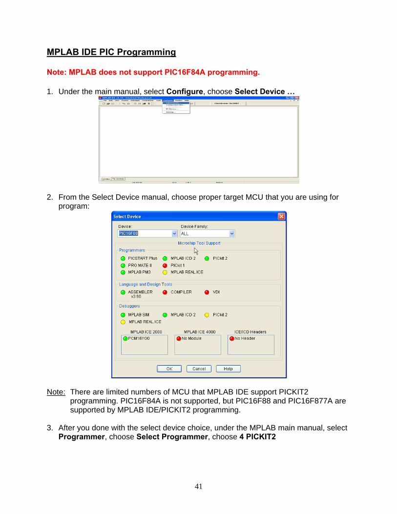
MPLAB IDE PIC Programming Note: MPLAB does not support PIC16F84A programming. 1. Under the main manual, select Configure, choose Select Device …
2. From the Select Device manual, choose proper target MCU that you are using for program:
Note: There are limited numbers of MCU that MPLAB IDE support PICKIT2 programming. PIC16F84A is not supported, but PIC16F88 and PIC16F877A are supported by MPLAB IDE/PICKIT2 programming. 3. After you done with the select device choice, under the MPLAB main manual, select Programmer, choose Select Programmer, choose 4 PICKIT2

42
4. After you choose the PICKIT2, the software will start the communication with the PIC Training System, if everything goes well, you should see this:
5. If you have the .HEX file ready, you can start programming the target MCU with MPLAB, under the main manual, select File, choose Import…
43
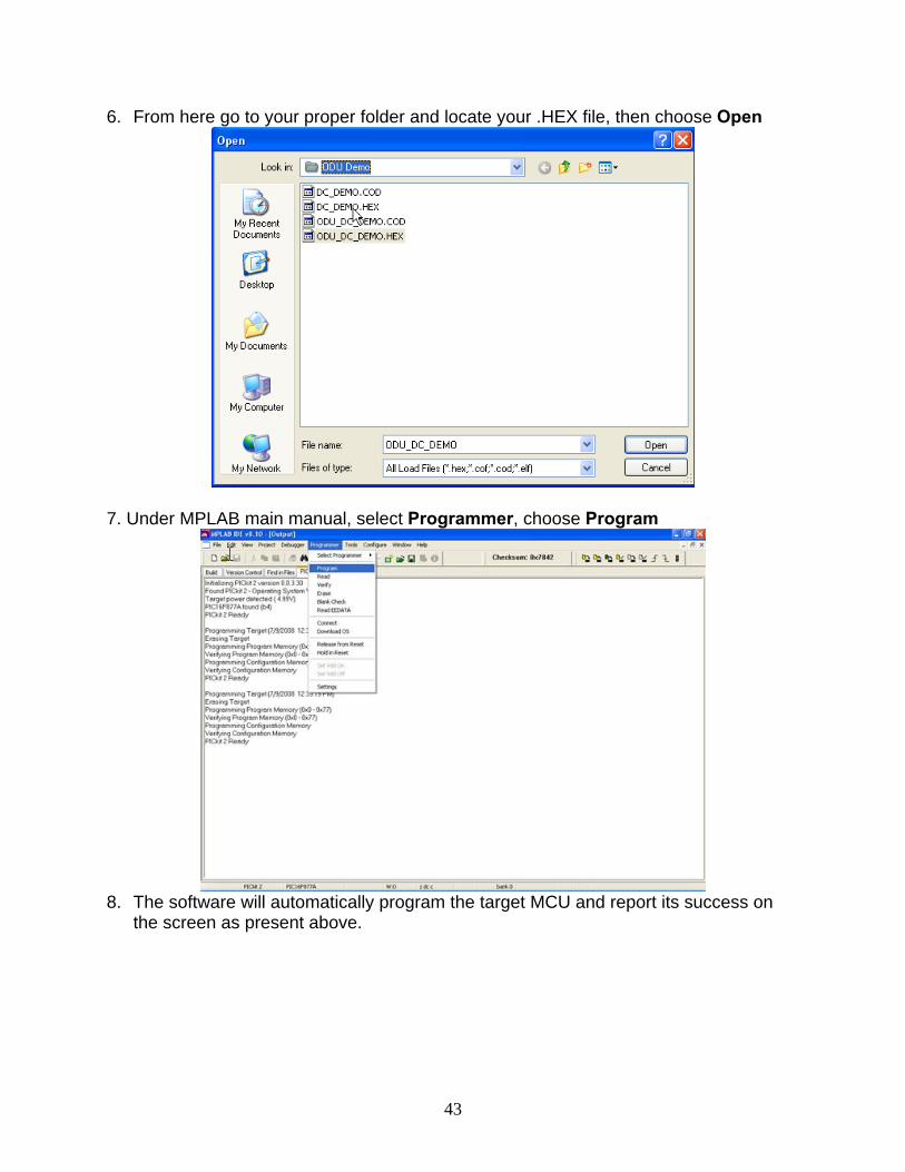
6. From here go to your proper folder and locate your .HEX file, then choose Open
7. Under MPLAB main manual, select Programmer, choose Program
8. The software will automatically program the target MCU and report its success on the screen as present above.

44
ICPROG PIC Programming Download icprog that is available from www.ic-prog.com Part I: (Try this one first, if doesn’t work, then try Part II) 1. Run downloaded icprog software. It is an exe file. 2. All hardware changes and driver installation will be made in the settings menu. Settings >> Device Select the proper PIC CPU that you are going to program with Settings >> Hardware Select Programmer: ElCheapo Programmer Port: LPT1 IO Delay: 12 Interface: Direct I/O Communication: Invert Data In Settings >> Options Select Misc: Process Priority: Normal Check Enable NT/2000/XP Driver: This will load the driver and follow the instruction From here you should be able to operate the IC-PROG software freely. Note: If you have different files, then follow Part II Part II: (You need icprog.exe, loaddrv.exe, giveio.sys, and giveio.cmd files) Download files from www.ic-prog.com: icprog.exe, giveio.sys, loaddrv.exe or make sure a zipped file has all four files in it. Note: If you have trouble in getting these files, bring your flash drive in my office during my office hours. Software installation: 1. Create a folder on your hard drive named ICPROG or any folder name of your choice. 2. Extract the zip file to the ICPROG folder or any folder name of your choice. Note: If you are using Windows NT/2000/XP you need go through Step #3 to install
45
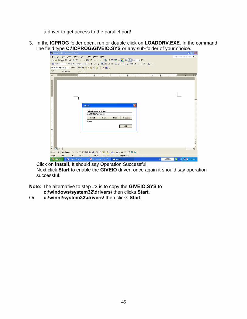
a driver to get access to the parallel port! 3. In the ICPROG folder open, run or double click on LOADDRV.EXE. In the command line field type C:\ICPROG\GIVEIO.SYS or any sub-folder of your choice.
Click on Install, It should say Operation Successful. Next click Start to enable the GIVEIO driver; once again it should say operation successful. Note: The alternative to step #3 is to copy the GIVEIO.SYS to c:\windows\system32\drivers\ then clicks Start. Or c:\winnt\system32\drivers\ then clicks Start.

46
Now you are ready to start the program. 4. In the ICPROG folder open, run, or double click ICPROG.EXE (It may be easier to create a shortcut on your desktop. Highlight ICPROG.EXE, right click then choose create shortcut, then copy it to main screen. Note: When you open the program it will probably give you a couple of errors. Right now, just ignore them for now they will be fixed momentarily. Software Configuration: Setup software to work with ODU PIC Programmer/ElCheapo Note: All hardware changes will be made in the settings menu. Settings >> Hardware (1) Select El Cheapo Programmer from the programmer menu. (2) Set I/O delay to 12 (3) Select Direct I/O on the interface menu. (4) Ensure Invert Data In is checked and that all others are unchecked. Click OK Note: At this point it may throw up some more error messages, continue to ignore them. Settings >> Options (1) On the Programming tab ensure verify after programming is checked and verify during programming is not.

47
(2) On the Misc. tab ensure enable NT/2000/XP driver is checked. Click OK Note: It will tell you it has to restart the program. Click OK, the program will close and then reopen. Once it reopens there should be no more error messages. Operation of This ICPROG Software: The software is now setup to use with all three of the chips: 16F84A, 16F877, 16F877A, and 16F88 (this needs ICPROGR version 1.05D). There are a big list of the PIC families are programmable through this software with ODU PIC programmer. Programming a chip 1, Select Chip from drop down menu. 2. File >> Open >> Select Files of type: IHX8files >> Open filename.HEX file. 3. Click program button or Select Program All from the command menu. Reading from a chip 1. Select chip from menu. 2. Click Read All button or select Read All from command menu. Note: The Configuration Word set up can be done through the menu selections on the right side of the screen. Note! Note!! 1. If you have problem to get the ICPROG software to work properly, try this: Under ICPROG menu, select Command, select Program Config, select Yes. 2. If you still have trouble in running ICPROG, try use LOADDRV.EXE to remove the GIVEIO.SYS drive then reboot your computer, then re-install the driver again. 3. There are skepticism about the compatibilities issues between ICPROG and Window XP SP2 system. Most of the incompatible issues were caused by different protection software such as virus scan, Window pop up blocker, firewall, software upgrade, setup, etc. that prevents ICPROG from gaining access of parallel port. I have used the ICPROG with Window XP SP2 and faced no problem! The BIOS set up in your computer should be: Parallel Port LPT1, Address = 378, Mode = EPP, IRQ = 7, Disable any MIDI