
PHYTER Extreme Temperature Single Port 10/100 Mb/s Ethernet ...
93
DP83848-EP PHYTER™ MILITARY TEMPERATURE SINGLE PORT 10/100 MB/S ETHERNET PHYSICAL LAYER TRANSCEIVER Data Manual PRODUCTION DATA information is current as of publication date. Products conform to specifications per the terms of the Texas Instruments standard warranty. Production processing does not necessarily include testing of all parameters. Literature Number: SLLSEC6D September 2012 – Revised June 2013
-
Upload
khangminh22 -
Category
Documents
-
view
2 -
download
0
Transcript of PHYTER Extreme Temperature Single Port 10/100 Mb/s Ethernet ...

DP83848-EPPHYTER™ MILITARY TEMPERATURE SINGLE PORT10/100 MB/S ETHERNET PHYSICAL LAYERTRANSCEIVER
Data Manual
PRODUCTION DATA information is current as of publication date.Products conform to specifications per the terms of the TexasInstruments standard warranty. Production processing does notnecessarily include testing of all parameters.
Literature Number: SLLSEC6D
September 2012–Revised June 2013

DP83848-EP
www.ti.com SLLSEC6D –SEPTEMBER 2012–REVISED JUNE 2013
Contents1 INTRODUCTION .................................................................................................................. 7
1.1 Features ...................................................................................................................... 71.2 Applications .................................................................................................................. 71.3 Supports Defense, Aerospace, and Medical Applications ............................................................. 71.4 Typical System Diagram ................................................................................................... 8
2 OVERVIEW ......................................................................................................................... 92.1 Description ................................................................................................................... 92.2 Ordering Information ........................................................................................................ 92.3 Device Information ........................................................................................................ 102.4 Terminal Descriptions ..................................................................................................... 12
3 ELECTRICAL SPECIFICATIONS .......................................................................................... 173.1 Absolute Maximum Ratings .............................................................................................. 173.2 Recommended Operating Conditions .................................................................................. 173.3 Thermal Information ....................................................................................................... 173.4 DC Specifications .......................................................................................................... 18
3.4.1 Electrical Characteristics ...................................................................................... 183.5 AC Specifications .......................................................................................................... 19
3.5.1 Power Up Timing ............................................................................................... 193.5.2 Reset Timing .................................................................................................... 203.5.3 MII Serial Management Timing ............................................................................... 213.5.4 100 Mb/s MII Transmit Timing ................................................................................ 213.5.5 100 Mb/s MII Receive Timing ................................................................................. 223.5.6 100BASE-TX Transmit Packet Latency Timing ............................................................. 223.5.7 100BASE-TX Transmit Packet Deassertion Timing ........................................................ 233.5.8 100BASE-TX Transmit Timing (tR/F & Jitter) ................................................................ 243.5.9 100BASE-TX Receive Packet Latency Timing ............................................................. 253.5.10 100BASE-TX Receive Packet Deassertion Timing ........................................................ 253.5.11 10 Mb/s MII Transmit Timing .................................................................................. 263.5.12 10 Mb/s MII Receive Timing .................................................................................. 263.5.13 10 Mb/s Serial Mode Transmit Timing ....................................................................... 273.5.14 10 Mb/s Serial Mode Receive Timing ........................................................................ 273.5.15 10BASE-T Transmit Timing (Start of Packet) ............................................................... 283.5.16 10BASE-T Transmit Timing (End of Packet) ................................................................ 283.5.17 10BASE-T Receive Timing (Start of Packet) ............................................................... 293.5.18 10BASE-T Receive Timing (End of Packet) ................................................................ 293.5.19 10 Mb/s Heartbeat Timing ..................................................................................... 303.5.20 10 Mb/s Jabber Timing ........................................................................................ 303.5.21 10BASE-T Normal Link Pulse Timing ........................................................................ 303.5.22 Auto-Negotiation Fast Link Pulse (FLP) Timing ............................................................ 313.5.23 100BASE-TX Signal Detect Timing .......................................................................... 313.5.24 100 Mb/s Internal Loopback Timing .......................................................................... 323.5.25 10 Mb/s Internal Loopback Timing ........................................................................... 333.5.26 RMII Transmit Timing .......................................................................................... 343.5.27 RMII Receive Timing ........................................................................................... 353.5.28 Isolation Timing ................................................................................................. 363.5.29 25 MHz_OUT Timing ........................................................................................... 36
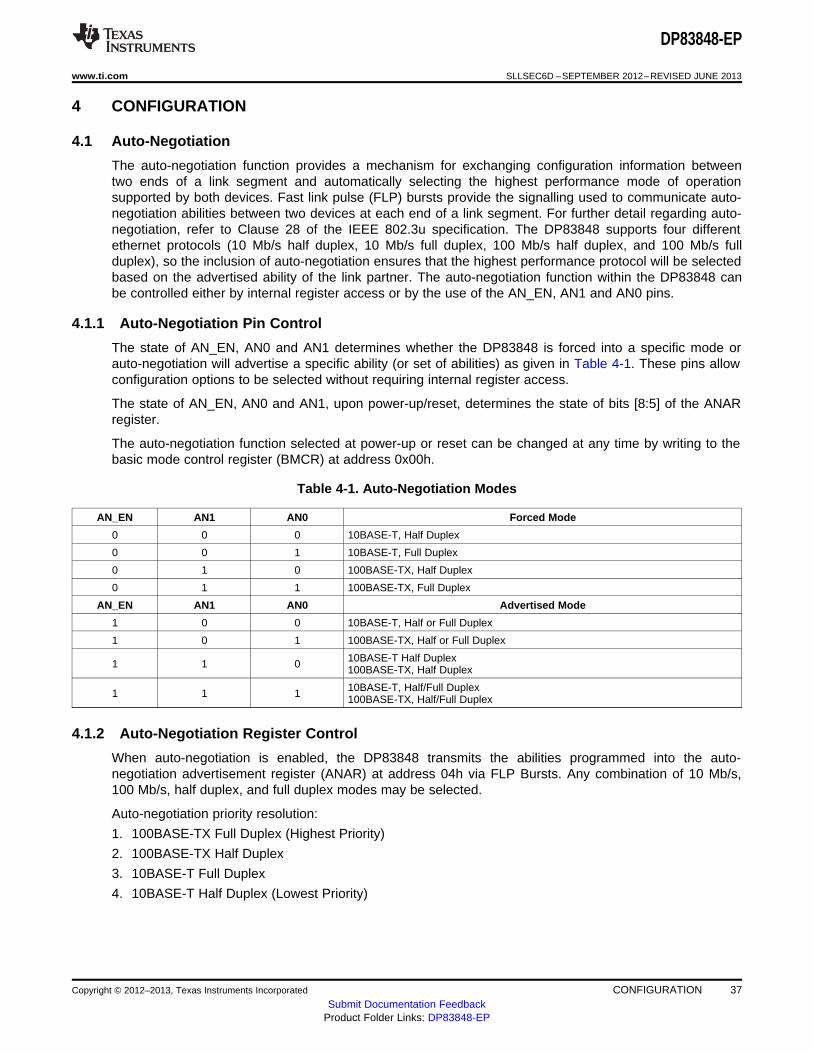
4 CONFIGURATION .............................................................................................................. 374.1 Auto-Negotiation ........................................................................................................... 37
4.1.1 Auto-Negotiation Pin Control .................................................................................. 374.1.2 Auto-Negotiation Register Control ............................................................................ 374.1.3 Auto-Negotiation Parallel Detection .......................................................................... 38
2 Contents Copyright © 2012–2013, Texas Instruments Incorporated

DP83848-EP
www.ti.com SLLSEC6D –SEPTEMBER 2012–REVISED JUNE 2013
4.1.4 Auto-Negotiation Restart ...................................................................................... 384.1.5 Enabling Auto-Negotiation via Software ..................................................................... 394.1.6 Auto-Negotiation Complete Time ............................................................................. 39
4.2 Auto-MDIX .................................................................................................................. 394.3 PHY Address ............................................................................................................... 39
4.3.1 MII Isolate Mode ................................................................................................ 404.4 LED Interface .............................................................................................................. 40
4.4.1 LEDs ............................................................................................................. 414.4.2 LED Direct Control ............................................................................................. 42
4.5 Half Duplex vs Full Duplex ............................................................................................... 424.6 Internal Loopback ......................................................................................................... 424.7 BIST ......................................................................................................................... 43
5 FUNCTIONAL DESCRIPTION ............................................................................................... 445.1 MII Interface ................................................................................................................ 44
5.1.1 Nibble-Wide MII Data Interface ............................................................................... 445.1.2 Collision Detect ................................................................................................. 445.1.3 Carrier Sense ................................................................................................... 45
5.2 Reduced MII Interface .................................................................................................... 455.3 10 Mb Serial Network Interface (SNI) .................................................................................. 465.4 802.3u MII Serial Management Interface ............................................................................... 46
5.4.1 Serial Management Register Access ........................................................................ 465.4.2 Serial Management Access Protocol ........................................................................ 465.4.3 Serial Management Preamble Suppression ................................................................ 47
6 ARCHITECTURE ................................................................................................................ 486.1 100BASE-TX Transmitter ................................................................................................ 48
6.1.1 Code-Group Encoding and Injection ......................................................................... 496.1.2 Scrambler ........................................................................................................ 506.1.3 NRZ to NRZI Encoder .......................................................................................... 506.1.4 Binary to MLT-3 Convertor .................................................................................... 50
6.2 100BASE-TX Receiver ................................................................................................... 506.2.1 Analog Front End ............................................................................................... 516.2.2 Digital Signal Processor ....................................................................................... 51
6.2.2.1 Digital Adaptive Equalization and Gain Control ................................................ 526.2.2.2 Base Line Wander Compensation ............................................................... 53
6.2.3 Signal Detect .................................................................................................... 536.2.4 MLT-3 to NRZI Decoder ....................................................................................... 536.2.5 NRZI to NRZ .................................................................................................... 536.2.6 Serial to Parallel ................................................................................................ 546.2.7 Descrambler ..................................................................................................... 546.2.8 Code-Group Alignment ........................................................................................ 546.2.9 4B/5B Decoder .................................................................................................. 546.2.10 100BASE-TX Link Integrity Monitor .......................................................................... 546.2.11 Bad SSD Detection ............................................................................................. 55
6.3 10BASE-T Transceiver Module .......................................................................................... 556.3.1 Operational Modes ............................................................................................. 55
6.3.1.1 Half Duplex Mode .................................................................................. 556.3.1.2 Full Duplex Mode .................................................................................. 55
6.3.2 Smart Squelch .................................................................................................. 556.3.3 Collision Detection and SQE .................................................................................. 566.3.4 Carrier Sense ................................................................................................... 566.3.5 Normal Link Pulse Detection/Generation .................................................................... 566.3.6 Jabber Function ................................................................................................. 566.3.7 Automatic Link Polarity Detection and Correction .......................................................... 57
Copyright © 2012–2013, Texas Instruments Incorporated Contents 3
DP83848-EP
SLLSEC6D –SEPTEMBER 2012–REVISED JUNE 2013 www.ti.com
6.3.8 Transmit and Receive Filtering ............................................................................... 576.3.9 Transmitter ...................................................................................................... 576.3.10 Receiver ......................................................................................................... 57
7 DESIGN GUIDELINES ......................................................................................................... 587.1 TPI Network Circuit ........................................................................................................ 587.2 ESD Protection ............................................................................................................ 587.3 Clock In (X1) Requirements .............................................................................................. 58
7.3.1 Oscillator ......................................................................................................... 587.3.2 Crystal ............................................................................................................ 59
7.4 Power Feedback Circuit .................................................................................................. 607.5 Power Down and Interrupt ............................................................................................... 60
7.5.1 Power Down Control Mode .................................................................................... 607.5.2 Interrupt Mechanisms .......................................................................................... 60
7.6 Energy Detect Mode ...................................................................................................... 617.7 Thermal Vias Recommendation ......................................................................................... 61
8 RESET OPERATION ........................................................................................................... 638.1 Hardware Reset ........................................................................................................... 638.2 Software Reset ............................................................................................................ 63
9 REGISTER BLOCK ............................................................................................................. 649.1 ................................................................................................................................ 649.2 Register Definition ......................................................................................................... 68
9.2.1 Basic Mode Control Register (BMCR) ....................................................................... 689.2.2 Basic Mode Status Register (BMSR) ........................................................................ 699.2.3 PHY Identifier Register #1 (PHYIDR1) ...................................................................... 709.2.4 PHY Identifier Register #2 (PHYIDR2) ...................................................................... 709.2.5 Auto-Negotiation Advertisement Register (ANAR) ......................................................... 719.2.6 Auto-Negotiation Link Partner Ability Register (ANLPAR) (BASE Page) ............................... 729.2.7 Auto-Negotiation Link Partner Ability Register (ANLPAR) (Next Page) ................................. 729.2.8 Auto-Negotiate Expansion Register (ANER) ................................................................ 739.2.9 Auto-Negotiation Next Page Transmit Register (ANNPTR) ............................................... 74
9.3 Extended Registers ....................................................................................................... 749.3.1 PHY Status Register (PHYSTS) .............................................................................. 749.3.2 MII Interrupt Control Register (MICR) ........................................................................ 769.3.3 MII Interrupt Status and Miscellaneous Control Register (MISR) ........................................ 779.3.4 False Carrier Sense Counter Register (FCSCR) ........................................................... 789.3.5 Receiver Error Counter Register (RECR) ................................................................... 789.3.6 100 Mb/s PCS Configuration and Status Register (PCSR) ............................................... 789.3.7 RMII and Bypass Register (RBR) ............................................................................ 799.3.8 LED Direct Control Register (LEDCR) ....................................................................... 809.3.9 PHY Control Register (PHYCR) .............................................................................. 809.3.10 10Base-T Status/Control Register (10BTSCR) ............................................................. 829.3.11 CD Test and BIST Extensions Register (CDCTRL1) ...................................................... 839.3.12 Energy Detect Control (EDCR) ............................................................................... 83
4 Contents Copyright © 2012–2013, Texas Instruments Incorporated

DP83848-EP
www.ti.com SLLSEC6D –SEPTEMBER 2012–REVISED JUNE 2013
List of Figures2-1 Device Block Diagram ........................................................................................................... 10
3-1 DP83848-EP Operating Life Derating Chart.................................................................................. 19
3-2 Power Up Timing ................................................................................................................. 19
3-3 Reset Timing ...................................................................................................................... 20
3-4 MII Serial Management Timing ................................................................................................. 21
3-5 100 Mb/s MII Transmit Timing .................................................................................................. 21
3-6 100 Mb/s MII Receive Timing................................................................................................... 22
3-7 100BASE-TX Transmit Packet Latency Timing .............................................................................. 22
3-8 100BASE-TX Transmit Packet Deassertion Timing ......................................................................... 23
3-9 100BASE-TX Transmit Timing (tR/F & Jitter) .................................................................................. 24
3-10 100BASE-TX Receive Packet Latency Timing ............................................................................... 25
3-11 100BASE-TX Receive Packet Deassertion Timing .......................................................................... 25
3-12 10 Mb/s MII Transmit Timing ................................................................................................... 26
3-13 10 Mb/s MII Receive Timing .................................................................................................... 26
3-14 10 Mb/s Serial Mode Transmit Timing......................................................................................... 27
3-15 10 Mb/s Serial Mode Receive Timing ......................................................................................... 27
3-16 10BASE-T Transmit Timing (Start of Packet) ................................................................................ 28
3-17 10BASE-T Transmit Timing (End of Packet) ................................................................................. 28
3-18 10BASE-T Receive Timing (Start of Packet) ................................................................................. 29
3-19 10BASE-T Receive Timing (End of Packet) .................................................................................. 29
3-20 10 Mb/s Heartbeat Timing....................................................................................................... 30
3-21 10 Mb/s Jabber Timing .......................................................................................................... 30
3-22 10BASE-T Normal Link Pulse Timing ......................................................................................... 30
3-23 Auto-Negotiation Fast Link Pulse (FLP) Timing .............................................................................. 31
3-24 100BASE-TX Signal Detect Timing ............................................................................................ 31
3-25 100 Mb/s Internal Loopback Timing ........................................................................................... 32
3-26 10 Mb/s Internal Loopback Timing ............................................................................................. 33
3-27 RMII Transmit Timing ............................................................................................................ 34
3-28 RMII Receive Timing............................................................................................................. 35
3-29 Isolation Timing ................................................................................................................... 36
3-30 25 MHz_OUT Timing ............................................................................................................ 36
4-1 PHYAD Strapping Example ..................................................................................................... 40
4-2 AN Strapping and LED Loading Example..................................................................................... 42
5-1 Typical MDC/MDIO Read Operation........................................................................................... 47
5-2 Typical MDC/MDIO Write Operation........................................................................................... 47
6-1 100BASE-TX Transmit Block Diagram ........................................................................................ 48
6-2 100BASE-TX Receive Block Diagram......................................................................................... 51
6-3 EIA/TIA Attenuation vs. Frequency for 0, 50, 100, 130 and 150 meters of CAT 5 cable............................... 53
6-4 100BASE-TX BLW Event ....................................................................................................... 53
6-5 10BASE-T Twisted Pair Smart Squelch Operation .......................................................................... 56
7-1 10/100 Mb/s Twisted Pair Interface ............................................................................................ 58
7-2 Crystal Oscillator Circuit ......................................................................................................... 59
7-3 Power Feedback Connection ................................................................................................... 60
7-4 Top View, Thermal Vias for GNDPAD, Pin 49 ............................................................................... 62
Copyright © 2012–2013, Texas Instruments Incorporated List of Figures 5

DP83848-EP
SLLSEC6D –SEPTEMBER 2012–REVISED JUNE 2013 www.ti.com
List of Tables2-1 Serial Management Interface ................................................................................................... 12
2-2 MAC Data Interface .............................................................................................................. 12
2-3 Clock Interface.................................................................................................................... 13
2-4 LED Interface ..................................................................................................................... 14
2-5 JTAG Interface.................................................................................................................... 14
2-6 Reset and Power Down ......................................................................................................... 14
2-7 Strap Options ..................................................................................................................... 15
2-8 10 Mb/s and 100 Mb/s PMD Interface......................................................................................... 16
2-9 Special Connections ............................................................................................................. 16
2-10 Power Supply Pins ............................................................................................................... 16
4-1 Auto-Negotiation Modes......................................................................................................... 37
4-2 PHY Address Mapping .......................................................................................................... 39
4-3 LED Mode Select................................................................................................................. 41
5-1 Supported Packet Sizes at ±50ppm and ±100ppm for Each Clock ....................................................... 45
5-2 Typical MDIO Frame Format ................................................................................................... 47
6-1 4B5B Code-Group Encoding or Decoding .................................................................................... 49
7-1 25 MHz Oscillator Specification ................................................................................................ 59
7-2 50 MHz Oscillator Specification ................................................................................................ 59
7-3 25 MHz Crystal Specification ................................................................................................... 60
9-1 Register Map...................................................................................................................... 64
9-2 Register Table .................................................................................................................... 65
9-3 Basic Mode Control Register (BMCR), Address 0x00....................................................................... 68
9-4 Basic Mode Status Register (BMSR), Address 0x01........................................................................ 69
9-5 PHY Identifier Register #1 (PHYIDR1), Address 0x02 ...................................................................... 70
9-6 PHY Identifier Register #2 (PHYIDR2), Address 0x03 ...................................................................... 70
9-7 Negotiation Advertisement Register (ANAR), Address 0x04 ............................................................... 71
9-8 Auto-Negotiation Link Partner Ability Register (ANLPAR) (BASE Page), Address 0x05 ............................... 72
9-9 Auto-Negotiation Link Partner Ability Register (ANLPAR) (Next Page), Address 0x05................................. 72
9-10 Auto-Negotiate Expansion Register (ANER), Address 0x06 ............................................................... 73
9-11 Auto-Negotiation Next Page Transmit Register (ANNPTR), Address 0x07 .............................................. 74
9-12 PHY Status Register (PHYSTS), Address 0x10 ............................................................................. 74
9-13 MII Interrupt Control Register (MICR), Address 0x11 ....................................................................... 76
9-14 MII Interrupt Status and Miscellaneous Control Register (MISR), Address 0x12........................................ 77
9-15 False Carrier Sense Counter Register (FCSCR), Address 0x14 .......................................................... 78
9-16 Receiver Error Counter Register (RECR), Address 0x15................................................................... 78
9-17 100 Mb/s PCS Configuration and Status Register (PCSR), Address 0x16............................................... 78
9-18 RMII and Bypass Register (RBR), Addresses 0x17 ......................................................................... 79
9-19 LED Direct Control Register (LEDCR), Address 0x18 ...................................................................... 80
9-20 PHY Control Register (PHYCR), Address 0x19.............................................................................. 80
9-21 10Base-T Status/Control Register (10BTSCR), Address 0x1A ............................................................ 82
9-22 CD Test and BIST Extensions Register (CDCTRL1), Address 0x1B ..................................................... 83
9-23 Energy Detect Control (EDCR), Address 0x1D .............................................................................. 83
6 List of Tables Copyright © 2012–2013, Texas Instruments Incorporated

DP83848-EP
www.ti.com SLLSEC6D –SEPTEMBER 2012–REVISED JUNE 2013
PHYTER™ MILITARY TEMPERATURE SINGLE PORT 10/100 MB/S ETHERNET PHYSICALLAYER TRANSCEIVERCheck for Samples: DP83848-EP
1 INTRODUCTION
1.1 Features12• Low-Power 3.3-V, 0.18-μm CMOS Technology• Low Power Consumption < 270 mW Typical• 3.3-V MAC Interface• Auto-MDIX for 10/100 Mb/s• Energy Detection Mode• 25-MHz Clock Out• SNI Interface (Configurable)• RMII Rev. 1.2 Interface (Configurable)• MII Serial Management Interface (MDC and MDIO)• IEEE 802.3u MII• IEEE 802.3u Auto-Negotiation and Parallel Detection• IEEE 802.3u ENDEC, 10BASE-T Transceivers and Filters• IEEE 802.3u PCS, 100BASE-TX Transceivers and Filters• IEEE 1149.1 JTAG• Integrated ANSI X3.263 Compliant TP-PMD Physical Sublayer with Adaptive Equalization and Baseline
Wander Compensation• Error-Free Operation up to 150 meters• Programmable LED Support Link, 10 /100 Mb/s Mode, Activity, and Collision Detect• Single Register Access for Complete PHY Status• 10/100 Mb/s Packet BIST (Built in Self Test)• Lead Free 48-Pin PQFP Package (7mm) x (7mm)
1.2 Applications• Automotive and Transportation• Industrial Controls and Factory Automation• General Embedded Applications
1.3 Supports Defense, Aerospace, and Medical Applications• Controlled Baseline• One Assembly and Test Site• One Fabrication Site• Military Temperature Range (-55°C to 125°C)• Extended Product Life Cycle• Extended Product-Change Notification• Product Traceability
1
Please be aware that an important notice concerning availability, standard warranty, and use in critical applications ofTexas Instruments semiconductor products and disclaimers thereto appears at the end of this data sheet.
2PHYTER is a trademark of Texas Instruments.
PRODUCTION DATA information is current as of publication date. Products conform to Copyright © 2012–2013, Texas Instruments Incorporatedspecifications per the terms of the Texas Instruments standard warranty. Productionprocessing does not necessarily include testing of all parameters.

MPU/CPU
Media
Access C
ontr
olle
r
MII/RMII/SNI
Magnetics
RJ-4
5
DP83848
10/100 MB/S
10Base-Tor
100Base-T
StatusLEDs
25-MHZClock
Source
Typical Application
DP83848-EP
SLLSEC6D –SEPTEMBER 2012–REVISED JUNE 2013 www.ti.com
1.4 Typical System Diagram
8 INTRODUCTION Copyright © 2012–2013, Texas Instruments Incorporated
Submit Documentation FeedbackProduct Folder Links: DP83848-EP

DP83848-EP
www.ti.com SLLSEC6D –SEPTEMBER 2012–REVISED JUNE 2013
2 OVERVIEW
2.1 Description
The number of applications requiring ethernet connectivity continues to increase. Along with this increasedmarket demand is a change in application requirements. The DP83848 was designed to allow ethernetconnectivity in the harshest environments. Our device meets IEEE 802.3u standards over a militarytemperature range of -55°C to 125°C. This device is ideally suited for harsh environments for examplewireless remote base stations, automotive, transportation and industrial control applications.
The DP83848 is a highly reliable, feature rich robust device which includes enhanced ESD protection, MIIand RMII for maximum flexibility in MPU selection all in a 48 pin PQFP package.
The DP83848 features integrated sublayers to support both 10BASE-T and 100BASE-TX Ethernetprotocols, which ensures compatibility and interoperability with all other standards based Ethernetsolutions.
2.2 Ordering Information (1)
TA PACKAGE ORDERABLE PART NUMBER TOP-SIDE MARKING VID NUMBER
DP83848MPHPREP Tape and Reel, 1000 V62/12615-01XE–55°C to PQFP-PHP DP83848EP125°C DP83848MPHPEP Tray, 1250 V62/12615-01XE-R
(1) For the most current package and ordering information, see the Package Option Addendum at the end of this document, or see the TIwebsite at www.ti.com.
Copyright © 2012–2013, Texas Instruments Incorporated OVERVIEW 9Submit Documentation Feedback
Product Folder Links: DP83848-EP
TX
_C
LK
TX
D[3
:0]
TX
_E
N
MD
IO
MD
C
CO
L
CR
S/C
RS
_D
V
RX
_E
R
RX
_D
V
RX
D[3
:0]
RX
_C
LK
RX_DATARX_CLK
REFERENCE CLOCKTD± RD± LEDs
MII/RMII/SNI Interfaces
Auto-MDIX
DAC ADC
JTAG
MII/RMII/SNI
SerialManagement
TX_DATA TX_CLK
10Base-T and100Base-TX
10Base-T and100Base-TX
TransmitBlock
ReceiveBlock
MIRegisters
Auto-NegotiationState Machine
ClockGeneration
BoundaryScan
LEDDrivers
DP83848-EP
SLLSEC6D –SEPTEMBER 2012–REVISED JUNE 2013 www.ti.com
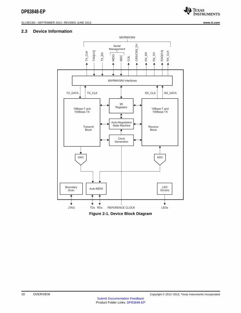
2.3 Device Information
Figure 2-1. Device Block Diagram
10 OVERVIEW Copyright © 2012–2013, Texas Instruments Incorporated
Submit Documentation FeedbackProduct Folder Links: DP83848-EP
DG
ND
IOG
ND
X1
X2
IOV
DD
33
MD
C
MD
IO
RE
SE
T_N
LE
D_L
INK
/AN
0
LE
D_
SP
EE
D/A
N1
LE
D_A
CT
/CO
L/A
N_E
N
25M
Hz_O
UT
RBIAS
PFBOUT
AVDD33
RESERVED
RESERVED
AGND
PFBIN1
TD +
TD –
AGND
RD +
RD –
TX
_C
LK
TX
_E
N
TX
D_0
TX
D_1
TX
D_2
TX
D_
3/S
NI_
MO
DE
PW
R_D
OW
N/I
NT
TC
K
TD
O
TM
S
TR
ST
TD
I
1 2 3 4 5 6 7 8 9 10
11
38
39
40
41
42
43
44
45
46
47
48
35
34
33
32 31
30
29
28
27
26
25
23
22
21
20
19
18
17
16
15
14
13
PFBIN2
RX_CLK
RX_DV/MII_MODE
CRS/CRS_DV/LED_CFG
RX_ER/MDIX_EN
COL/PHYAD0
RXD_0/PHYAD1
RXD_1/PHYAD2
RXD_2/PHYAD3
RXD_3/PHYAD4
IOGND
IOVDD33
2437
36
12
Thermal Pad
DP83848-EP
www.ti.com SLLSEC6D –SEPTEMBER 2012–REVISED JUNE 2013
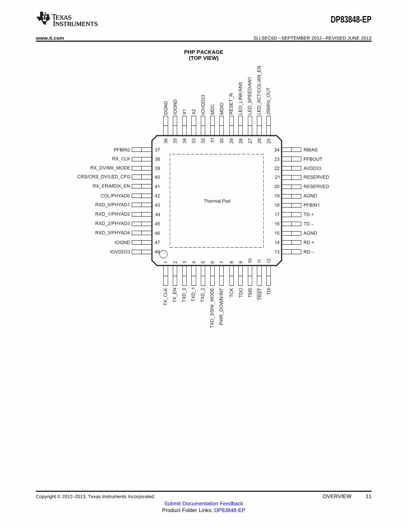
PHP PACKAGE(TOP VIEW)
Copyright © 2012–2013, Texas Instruments Incorporated OVERVIEW 11Submit Documentation Feedback
Product Folder Links: DP83848-EP

DP83848-EP
SLLSEC6D –SEPTEMBER 2012–REVISED JUNE 2013 www.ti.com
2.4 Terminal Descriptions
All DP83848 signal pins are I/O cells regardless of the particular use. The definitions below define thefunctionality of the I/O cells for each pin.
Type: I - Input
Type: O - Output
Type: I/O - Input/Output
Type OD - Open Drain
Type: PD, PU - Internal Pulldown/Pullup
Type: S - Strapping Pin (All strap pins have weak internal pull-ups or pull-downs. If the default strap valueis needed to be changed then an external 2.2 kΩ resistor should be used.)
Table 2-1. Serial Management Interface
TERMINALI/O DESCRIPTION
NAME NO.
MANAGEMENT DATA CLOCK: Synchronous clock to the MDIO management data input/output serial interfaceMDC 31 I which may be asynchronous to transmit and receive clocks. The maximum clock rate is 25 MHz with no minimum
clock rate.
MANAGEMENT DATA I/O: Bi-directional management instruction/ data signal that may be sourced by the stationMDIO 30 I/O management entity or the PHY. This pin requires a 1.5 kΩ pullup resistor.
Table 2-2. MAC Data Interface
TERMINALI/O DESCRIPTION
NAME NO.
MII TRANSMIT CLOCK: 25 MHz Transmit clock output in 100 Mb/s mode or 2.5 MHz in 10 Mb/s mode derivedfrom the 25 MHz reference clock.
Unused in RMII mode. The device uses the X1 reference clock input as the 50 MHz reference for both transmitTX_CLK 1 O and receive.
SNI TRANSMIT CLOCK: 10 MHz Transmit clock output in 10 Mb SNI mode. The MAC should source TX_ENand TXD_0 using this clock.
MII TRANSMIT ENABLE: Active high input indicates the presence of valid data inputs on TXD[3:0].
TX_EN 2 I, PD RMII TRANSMIT ENABLE: Active high input indicates the presence of valid data on TXD[1:0].
SNI TRANSMIT ENABLE: Active high input indicates the presence of valid data on TXD_0.
MII TRANSMIT DATA: Transmit data MII input pins, TXD[3:0], that accept data synchronous to the TX_CLKTXD_0 3 I (2.5 MHz in 10 Mb/s mode or 25 MHz in 100 Mb/s mode).
RMII TRANSMIT DATA: Transmit data RMII input pins, TXD[1:0], that accept data synchronous to the 50 MHzTXD_1 4 reference clock.
TXD_2 5 SNI TRANSMIT DATA: Transmit data SNI input pin, TXD_0, that accept data synchronous to the TX_CLK(10 MHz in 10 Mb/s SNI mode).
TXD_3 6 S, I, PD
MII RECEIVE CLOCK: Provides the 25 MHz recovered receive clocks for 100 Mb/s mode and 2.5 MHz for10 Mb/s mode.
RX_CLK 38 O Unused in RMII mode. The device uses the X1 reference clock input as the 50 MHz reference for both transmitand receive.
SNI RECEIVE CLOCK: Provides the 10 MHz recovered receive clocks for 10 Mb/s SNI mode.
MII RECEIVE DATA VALID: Asserted high to indicate that valid data is present on the corresponding RXD[3:0].MII mode by default with internal pulldown.
RX_DV 39 S, O, PD RMII Synchronous Receive Data Valid: This signal provides the RMII Receive Data Valid indicationindependent of Carrier Sense.
This pin is not used in SNI mode.
12 OVERVIEW Copyright © 2012–2013, Texas Instruments Incorporated
Submit Documentation FeedbackProduct Folder Links: DP83848-EP
DP83848-EP
www.ti.com SLLSEC6D –SEPTEMBER 2012–REVISED JUNE 2013
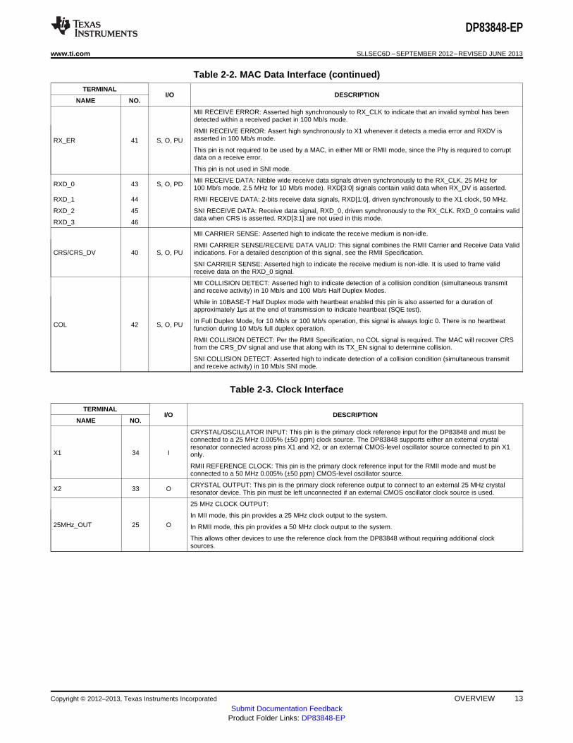
Table 2-2. MAC Data Interface (continued)TERMINAL
I/O DESCRIPTIONNAME NO.
MII RECEIVE ERROR: Asserted high synchronously to RX_CLK to indicate that an invalid symbol has beendetected within a received packet in 100 Mb/s mode.
RMII RECEIVE ERROR: Assert high synchronously to X1 whenever it detects a media error and RXDV isasserted in 100 Mb/s mode.RX_ER 41 S, O, PUThis pin is not required to be used by a MAC, in either MII or RMII mode, since the Phy is required to corruptdata on a receive error.
This pin is not used in SNI mode.
MII RECEIVE DATA: Nibble wide receive data signals driven synchronously to the RX_CLK, 25 MHz forRXD_0 43 S, O, PD 100 Mb/s mode, 2.5 MHz for 10 Mb/s mode). RXD[3:0] signals contain valid data when RX_DV is asserted.
RXD_1 44 RMII RECEIVE DATA: 2-bits receive data signals, RXD[1:0], driven synchronously to the X1 clock, 50 MHz.
RXD_2 45 SNI RECEIVE DATA: Receive data signal, RXD_0, driven synchronously to the RX_CLK. RXD_0 contains validdata when CRS is asserted. RXD[3:1] are not used in this mode.
RXD_3 46
MII CARRIER SENSE: Asserted high to indicate the receive medium is non-idle.
RMII CARRIER SENSE/RECEIVE DATA VALID: This signal combines the RMII Carrier and Receive Data ValidCRS/CRS_DV 40 S, O, PU indications. For a detailed description of this signal, see the RMII Specification.
SNI CARRIER SENSE: Asserted high to indicate the receive medium is non-idle. It is used to frame validreceive data on the RXD_0 signal.
MII COLLISION DETECT: Asserted high to indicate detection of a collision condition (simultaneous transmitand receive activity) in 10 Mb/s and 100 Mb/s Half Duplex Modes.
While in 10BASE-T Half Duplex mode with heartbeat enabled this pin is also asserted for a duration ofapproximately 1μs at the end of transmission to indicate heartbeat (SQE test).
In Full Duplex Mode, for 10 Mb/s or 100 Mb/s operation, this signal is always logic 0. There is no heartbeatCOL 42 S, O, PU function during 10 Mb/s full duplex operation.
RMII COLLISION DETECT: Per the RMII Specification, no COL signal is required. The MAC will recover CRSfrom the CRS_DV signal and use that along with its TX_EN signal to determine collision.
SNI COLLISION DETECT: Asserted high to indicate detection of a collision condition (simultaneous transmitand receive activity) in 10 Mb/s SNI mode.
Table 2-3. Clock Interface
TERMINALI/O DESCRIPTION
NAME NO.
CRYSTAL/OSCILLATOR INPUT: This pin is the primary clock reference input for the DP83848 and must beconnected to a 25 MHz 0.005% (±50 ppm) clock source. The DP83848 supports either an external crystalresonator connected across pins X1 and X2, or an external CMOS-level oscillator source connected to pin X1
X1 34 I only.
RMII REFERENCE CLOCK: This pin is the primary clock reference input for the RMII mode and must beconnected to a 50 MHz 0.005% (±50 ppm) CMOS-level oscillator source.
CRYSTAL OUTPUT: This pin is the primary clock reference output to connect to an external 25 MHz crystalX2 33 O resonator device. This pin must be left unconnected if an external CMOS oscillator clock source is used.
25 MHz CLOCK OUTPUT:
In MII mode, this pin provides a 25 MHz clock output to the system.25MHz_OUT 25 O In RMII mode, this pin provides a 50 MHz clock output to the system.
This allows other devices to use the reference clock from the DP83848 without requiring additional clocksources.
Copyright © 2012–2013, Texas Instruments Incorporated OVERVIEW 13Submit Documentation Feedback
Product Folder Links: DP83848-EP

DP83848-EP
SLLSEC6D –SEPTEMBER 2012–REVISED JUNE 2013 www.ti.com
Table 2-4. LED Interface
TERMINALI/O DESCRIPTION
NAME NO.
LINK LED: In Mode 1, this pin indicates the status of the LINK. The LED will be ON when Link is good.LED_LINK 28 S, O, PU LINK/ACT LED: In Mode 2 and Mode 3, this pin indicates transmit and receive activity in addition to the status of
the Link. The LED will be ON when Link is good. It will blink when the transmitter or receiver is active.
SPEED LED: The LED is ON when device is in 100 Mb/s and OFF when in 10 Mb/s. Functionality of this LED isLED_SPEED 27 S, O, PU independent of mode selected.
ACTIVITY LED: In Mode 1, this pin is the Activity LED which is ON when activity is present on either Transmit orReceive.
LED_ACT/COL 26 S, O, PUCOLLISION/DUPLEX LED: In Mode 2, this pin by default indicates Collision detection. For Mode 3, this LEDoutput may be programmed to indicate Full-duplex status instead of Collision.
Table 2-5. JTAG Interface
TERMINALI/O DESCRIPTION
NAME No.
TCK 8 I, PU TEST CLOCK: This pin has a weak internal pullup
TDI 12 I, PU TEST DATA INPUT: This pin has a weak internal pullup
TDO 9 O TEST OUTPUT
TMS 10 I, PU TEST MODE SELECT: This pin has a weak internal pullup
TRST# 11 I, PU TEST RESET: Active low asynchronous test reset. This pin has a weak internal pullup.
Table 2-6. Reset and Power Down
TERMINALI/O DESCRIPTION
NAME NO.
RESET: Active Low input that initializes or re-initializes the DP83848. Asserting this pin low for at least 1 μs willRESET_N 29 I, PU force a reset process to occur. All internal registers will re-initialize to their default states as specified for each bit
in the Register Block section. All strap options are re-initialized as well.
The default function of this pin is POWER DOWN.
POWER DOWN: The pin is an active low input in this mode and should be asserted low to put the device in aPower Down mode.
PWR_DOWN/INT 7 I, OD, PUINTERRUPT: The pin is an open drain output in this mode and will be asserted low when an interrupt conditionoccurs. Although the pin has a weak internal pull-up, some applications may require an external pull-up resister.Register access is required for the pin to be used as an interrupt mechanism. See Section 7.5.2 for more detailson the interrupt mechanisms.
14 OVERVIEW Copyright © 2012–2013, Texas Instruments Incorporated
Submit Documentation FeedbackProduct Folder Links: DP83848-EP
DP83848-EP
www.ti.com SLLSEC6D –SEPTEMBER 2012–REVISED JUNE 2013
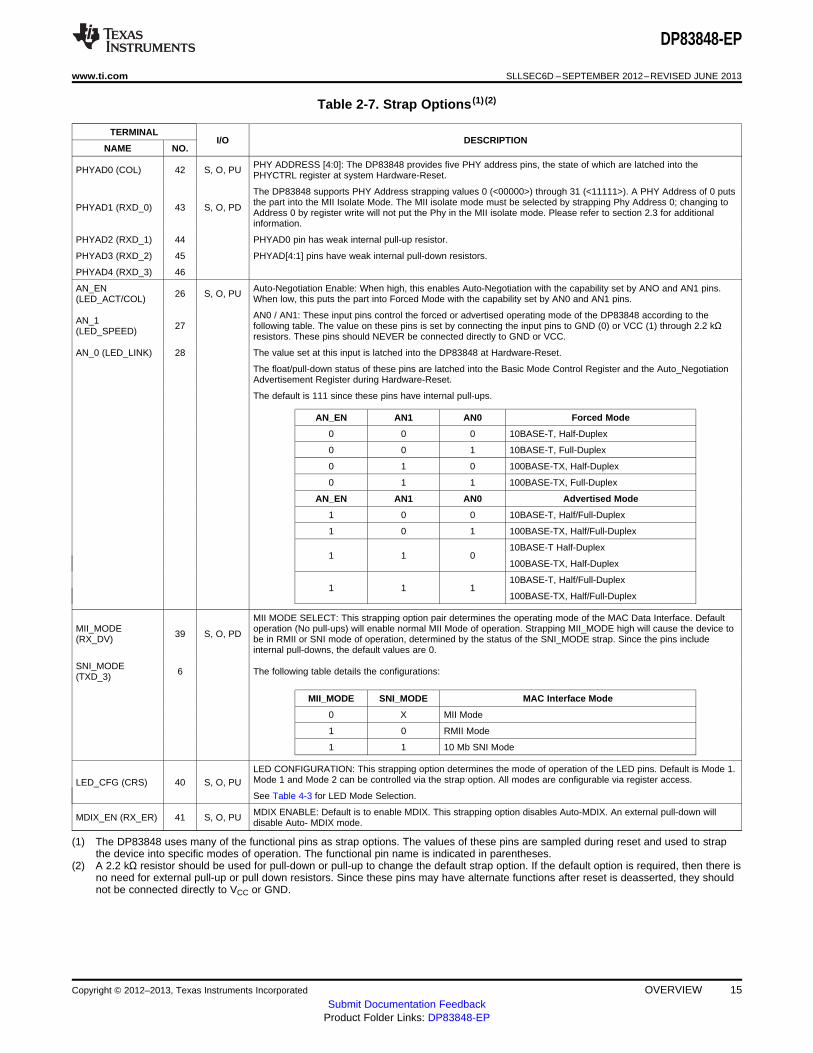
Table 2-7. Strap Options (1) (2)
TERMINALI/O DESCRIPTION
NAME NO.
PHY ADDRESS [4:0]: The DP83848 provides five PHY address pins, the state of which are latched into thePHYAD0 (COL) 42 S, O, PU PHYCTRL register at system Hardware-Reset.
The DP83848 supports PHY Address strapping values 0 (<00000>) through 31 (<11111>). A PHY Address of 0 putsthe part into the MII Isolate Mode. The MII isolate mode must be selected by strapping Phy Address 0; changing toPHYAD1 (RXD_0) 43 S, O, PD Address 0 by register write will not put the Phy in the MII isolate mode. Please refer to section 2.3 for additionalinformation.
PHYAD2 (RXD_1) 44 PHYAD0 pin has weak internal pull-up resistor.
PHYAD3 (RXD_2) 45 PHYAD[4:1] pins have weak internal pull-down resistors.
PHYAD4 (RXD_3) 46
AN_EN Auto-Negotiation Enable: When high, this enables Auto-Negotiation with the capability set by ANO and AN1 pins.26 S, O, PU(LED_ACT/COL) When low, this puts the part into Forced Mode with the capability set by AN0 and AN1 pins.
AN0 / AN1: These input pins control the forced or advertised operating mode of the DP83848 according to theAN_1 27 following table. The value on these pins is set by connecting the input pins to GND (0) or VCC (1) through 2.2 kΩ(LED_SPEED) resistors. These pins should NEVER be connected directly to GND or VCC.
AN_0 (LED_LINK) 28 The value set at this input is latched into the DP83848 at Hardware-Reset.
The float/pull-down status of these pins are latched into the Basic Mode Control Register and the Auto_NegotiationAdvertisement Register during Hardware-Reset.
The default is 111 since these pins have internal pull-ups.
AN_EN AN1 AN0 Forced Mode
0 0 0 10BASE-T, Half-Duplex
0 0 1 10BASE-T, Full-Duplex
0 1 0 100BASE-TX, Half-Duplex
0 1 1 100BASE-TX, Full-Duplex
AN_EN AN1 AN0 Advertised Mode
1 0 0 10BASE-T, Half/Full-Duplex
1 0 1 100BASE-TX, Half/Full-Duplex
10BASE-T Half-Duplex1 1 0
100BASE-TX, Half-Duplex
10BASE-T, Half/Full-Duplex1 1 1
100BASE-TX, Half/Full-Duplex
MII MODE SELECT: This strapping option pair determines the operating mode of the MAC Data Interface. DefaultMII_MODE operation (No pull-ups) will enable normal MII Mode of operation. Strapping MII_MODE high will cause the device to39 S, O, PD(RX_DV) be in RMII or SNI mode of operation, determined by the status of the SNI_MODE strap. Since the pins include
internal pull-downs, the default values are 0.
SNI_MODE 6 The following table details the configurations:(TXD_3)
MII_MODE SNI_MODE MAC Interface Mode
0 X MII Mode
1 0 RMII Mode
1 1 10 Mb SNI Mode
LED CONFIGURATION: This strapping option determines the mode of operation of the LED pins. Default is Mode 1.Mode 1 and Mode 2 can be controlled via the strap option. All modes are configurable via register access.LED_CFG (CRS) 40 S, O, PUSee Table 4-3 for LED Mode Selection.
MDIX ENABLE: Default is to enable MDIX. This strapping option disables Auto-MDIX. An external pull-down willMDIX_EN (RX_ER) 41 S, O, PU disable Auto- MDIX mode.
(1) The DP83848 uses many of the functional pins as strap options. The values of these pins are sampled during reset and used to strapthe device into specific modes of operation. The functional pin name is indicated in parentheses.
(2) A 2.2 kΩ resistor should be used for pull-down or pull-up to change the default strap option. If the default option is required, then there isno need for external pull-up or pull down resistors. Since these pins may have alternate functions after reset is deasserted, they shouldnot be connected directly to VCC or GND.
Copyright © 2012–2013, Texas Instruments Incorporated OVERVIEW 15Submit Documentation Feedback
Product Folder Links: DP83848-EP

DP83848-EP
SLLSEC6D –SEPTEMBER 2012–REVISED JUNE 2013 www.ti.com
Table 2-8. 10 Mb/s and 100 Mb/s PMD Interface
TERMINALI/O DESCRIPTION
NAME NO.
Differential common driver transmit output (PMD Output Pair). These differential outputs are automaticallyconfigured to either 10BASE-T or 100BASE-TX signaling.
TD-, TD+ 16, 17 I/O In Auto-MDIX mode of operation, this pair can be used as the Receive Input pair.
These pins require 3.3V bias for operation.
Differential receive input (PMD Input Pair). These differential inputs are automatically configured to accept either100BASE-TX or 10BASE-T signaling.
RD-, RD+ 13, 14 I/O In Auto-MDIX mode of operation, this pair can be used as the Transmit Output pair.
These pins require 3.3V bias for operation.
Table 2-9. Special Connections
TERMINALI/O DESCRIPTION
NAME NO.
RBIAS 24 I Bias Resistor Connection. A 4.87 kΩ 1% resistor should be connected from RBIAS to GND.
Power Feedback Output. Parallel caps, 10μ F (Tantalum preferred) and 0.1μF, should be placed close to thePFBOUT 23 O PFBOUT. Connect this pin to PFBIN1 (pin 18) and PFBIN2 (pin 37). See Section 5.4 for proper placement pin.
Power Feedback Input. These pins are fed with power from PFBOUT pin. A small capacitor of 0.1μF should bePFBIN1 18 I connected close to each pin.
PFBIN2 37 Note: Do not supply power to these pins other than from PFBOUT.
RESERVED 20, 21 I/O RESERVED: These pins must be pulled-up through 2.2 kΩ resistors to AVDD33 supply.
Table 2-10. Power Supply Pins
TERMINALDESCRIPTION
NAME NO.
IOVDD33 32, 48 I/O 3.3V Supply
IOGND 35, 47 I/O Ground
DGND 36 Digital Ground
AVDD33 22 Analog 3.3V Supply
AGND 15, 19 Analog Ground
GNDPAD Thermal Pad
16 OVERVIEW Copyright © 2012–2013, Texas Instruments Incorporated
Submit Documentation FeedbackProduct Folder Links: DP83848-EP

DP83848-EP
www.ti.com SLLSEC6D –SEPTEMBER 2012–REVISED JUNE 2013
3 ELECTRICAL SPECIFICATIONS
3.1 Absolute Maximum Ratingsover operating free-air temperature range (unless otherwise noted)
VALUE UNIT
VCC Supply voltage -0.5 to 4.2 V
VIN DC input voltage -0.5 to VCC + 0.5 V
VOUT DC output voltage -0.5 to VCC + 0.5 V
TSTG Storage temperature -65 to 150 °C
TJ Operating junction temperature -55 to 150 °C
TL Lead temperature (soldering, 10 seconds) 260 °C
ESD rating (RZAP = 1.5 kΩ, CZAP = 100 pF) 4 kV
3.2 Recommended Operating Conditions (1)
over operating free-air temperature range (unless otherwise noted)
MIN NOM MAX UNIT
VCC Supply voltage 3 3.6 V
TA Operating free-air temperature (2) -55 125 °C
PD Power dissipation 267 mW
(1) Absolute maximum ratings are those values beyond which the safety of the device cannot be guaranteed. They are not meant to implythat the device should be operated at these limits.
(2) Provided that Thermal Pad is soldered down.
3.3 Thermal InformationDP83848
THERMAL METRIC PHP UNITS
48 PINS
θJA Junction-to-ambient thermal resistance (1) 35.74
θJCtop Junction-to-case (top) thermal resistance (2) 21.8
θJB Junction-to-board thermal resistance (3) 19.5°C/W
ψJT Junction-to-top characterization parameter (4) 1.2
ψJB Junction-to-board characterization parameter (5) 19.4
θJCbot Junction-to-case (bottom) thermal resistance (6) 3.2
(1) The junction-to-ambient thermal resistance under natural convection is obtained in a simulation on a JEDEC-standard, high-K board, asspecified in JESD51-7, in an environment described in JESD51-2a.
(2) The junction-to-case (top) thermal resistance is obtained by simulating a cold plate test on the package top. No specific JEDEC-standard test exists, but a close description can be found in the ANSI SEMI standard G30-88.
(3) The junction-to-board thermal resistance is obtained by simulating in an environment with a ring cold plate fixture to control the PCBtemperature, as described in JESD51-8.
(4) The junction-to-top characterization parameter, ψJT, estimates the junction temperature of a device in a real system and is extractedfrom the simulation data for obtaining θJA, using a procedure described in JESD51-2a (sections 6 and 7).
(5) The junction-to-board characterization parameter, ψJB, estimates the junction temperature of a device in a real system and is extractedfrom the simulation data for obtaining θJA , using a procedure described in JESD51-2a (sections 6 and 7).
(6) The junction-to-case (bottom) thermal resistance is obtained by simulating a cold plate test on the exposed (power) pad. No specificJEDEC standard test exists, but a close description can be found in the ANSI SEMI standard G30-88.Spacer
Copyright © 2012–2013, Texas Instruments Incorporated ELECTRICAL SPECIFICATIONS 17Submit Documentation Feedback
Product Folder Links: DP83848-EP

1000.00
10000.00
100000.00
1000000.00
80 90 100 110 120 130 140 150 160
Esti
mate
d L
ife (
Ho
urs
)
Continuous TJ (°C)
DP83848-EP
SLLSEC6D –SEPTEMBER 2012–REVISED JUNE 2013 www.ti.com
3.4 DC Specifications
3.4.1 Electrical Characteristicsover operating free-air temperature range (unless otherwise noted)
PARAMETER TEST CONDITIONS MIN TYP MAX UNIT
VIH Input High Voltage Nominal VCC 2 V
VIL Input Low Voltage 0.8 V
IIH Input High Current VIN = VCC 10 µA
IIL Input Low Current VIN = GND 10 µA
VOL Output Low Voltage IOL = 4 mA 0.4 V
VOH Output High Voltage IOH = -4 mA VCC - 0.5 V
VOUT = VCCIOZ TRI-STATE Leakage ±10 µAVOUT = GND
VTPTD_100 100M Transmit Voltage 0.89 1 1.15 V
VTPTDsym 100M Transmit Voltage Symmetry ±2 %
VTPTD_10 10M Transmit Voltage 2.17 2.5 2.8 V
CIN1 CMOS Input Capacitance 5 pF
COUT1 CMOS Output Capacitance 5 pF
100BASE-TX Signal detect turnonSDTHon 1000 mV diff pk-pkthreshold
100BASE-TX Signal detect turnoffSDTHoff 200 mV diff pk-pkthreshold
VTH1 10BASE-T Receive Threshold 585 mV
Idd100 100BASE-TX (Full Duplex) 81 mA
Idd10 10BASE-T (Full Duplex) 92 mA
Idd Power Down Mode 14 mA
(1) See datasheet for absolute maximum and minimum recommended operating conditions.(2) Silicon operating life design goal is 10 years at 105°C junction temperature (does not include package interconnect life).(3) Enhanced plastic product disclaimer applies.
Figure 3-1. DP83848-EP Operating Life Derating Chart
18 ELECTRICAL SPECIFICATIONS Copyright © 2012–2013, Texas Instruments Incorporated
Submit Documentation FeedbackProduct Folder Links: DP83848-EP
T2.1.1
32 clocks
T2.1.2
T2.1.3
InputOutput
VCC
X1 clock
HardwareRESET_N
MDC
Latch-in of hardwareconfiguration pins
Dual function pinsbecome enabled as outputs
DP83848-EP
www.ti.com SLLSEC6D –SEPTEMBER 2012–REVISED JUNE 2013
3.5 AC Specifications
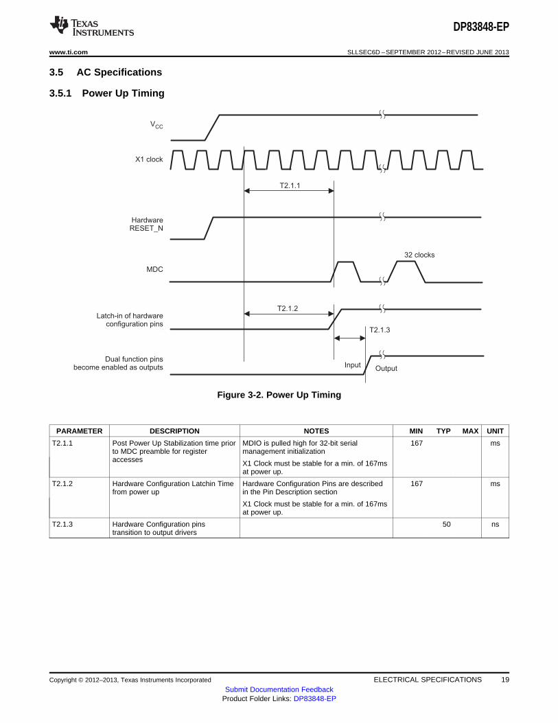
3.5.1 Power Up Timing
Figure 3-2. Power Up Timing
xxxPARAMETER DESCRIPTION NOTES MIN TYP MAX UNIT
T2.1.1 Post Power Up Stabilization time prior MDIO is pulled high for 32-bit serial 167 msto MDC preamble for register management initializationaccesses X1 Clock must be stable for a min. of 167ms
at power up.
T2.1.2 Hardware Configuration Latchin Time Hardware Configuration Pins are described 167 msfrom power up in the Pin Description section
X1 Clock must be stable for a min. of 167msat power up.
T2.1.3 Hardware Configuration pins 50 nstransition to output drivers
Copyright © 2012–2013, Texas Instruments Incorporated ELECTRICAL SPECIFICATIONS 19Submit Documentation Feedback
Product Folder Links: DP83848-EP

T2.2.4
T2.2.1
32 clocks
T2.2.2
T2.2.3
InputOutput
VCC
X1 clock
HardwareRESET_N
MDC
Latch-in of hardwareconfiguration pins
Dual function pinsbecome enabled as outputs
DP83848-EP
SLLSEC6D –SEPTEMBER 2012–REVISED JUNE 2013 www.ti.com
3.5.2 Reset Timing
Figure 3-3. Reset Timing
xxxPARAMETER DESCRIPTION NOTES (1) MIN TYP MAX UNIT
T2.2.1 Post RESET Stabilization time prior to MDIO is pulled high for 32-bit serial 3 µsMDC preamble for register accesses management initialization
T2.2.2 Hardware Configuration Latchin Time Hardware Configuration Pins are described 3 µsfrom the Deassertion of RESET (either in the Pin Description sectionsoft or hard)
T2.2.3 Hardware Configuration pins transition 50 nsto output drivers
T2.2.4 RESET pulse width X1 Clock must be stable for at min. of 1µs 1 µsduring RESET pulse low time
(1) It is important to choose pull-up and/or pull-down resistors for each of the hardware configuration pins that provide fast RC timeconstants in order to latch-in the proper value prior to the pin transitioning to an output driver.
20 ELECTRICAL SPECIFICATIONS Copyright © 2012–2013, Texas Instruments Incorporated
Submit Documentation FeedbackProduct Folder Links: DP83848-EP

TX_CLK
TXD[3:0]TX_EN Valid data
T2.4.1 T2.4.1
T2.4.2 T2.4.3
MDC
MDC
MDIO (output)
MDIO (input) Valid data
T2.3.1
T2.3.4
T2.3.2 T2.3.3
DP83848-EP
www.ti.com SLLSEC6D –SEPTEMBER 2012–REVISED JUNE 2013
3.5.3 MII Serial Management Timing
Figure 3-4. MII Serial Management Timing
xxxPARAMETER DESCRIPTION NOTES MIN TYP MAX UNIT
T2.3.1 MDC to MDIO (Output) Delay Time 0 30 ns
T2.3.2 MDIO (Input) to MDC Setup Time 10 ns
T2.3.3 MDIO (Input) to MDC Hold Time 10 ns
T2.3.4 MDC Frequency 2.5 25 MHz
3.5.4 100 Mb/s MII Transmit Timing
Figure 3-5. 100 Mb/s MII Transmit Timing
xxxPARAMETER DESCRIPTION NOTES MIN TYP MAX UNIT
T2.4.1 TX_CLK High/Low Time 100 Mb/s Normal mode 16 20 24 ns
T2.4.2 TXD[3:0], TX_EN Data Setup to 100 Mb/s Normal mode 9.70 nsTX_CLK
T2.4.3 TXD[3:0], TX_EN Data Hold from 100 Mb/s Normal mode 0 nsTX_CLK
Copyright © 2012–2013, Texas Instruments Incorporated ELECTRICAL SPECIFICATIONS 21Submit Documentation Feedback
Product Folder Links: DP83848-EP

TX_CLK
TX_EN
TXD
PMD output pair (J/K)
T2.6.1
IDLE DATA
RX_CLK
RXD[3:0]
RX_DVRX_ER
Valid data
T2.5.2
T2.5.1 T2.5.1
DP83848-EP
SLLSEC6D –SEPTEMBER 2012–REVISED JUNE 2013 www.ti.com
3.5.5 100 Mb/s MII Receive Timing
Figure 3-6. 100 Mb/s MII Receive Timing
xxxPARAMETER DESCRIPTION NOTES MIN TYP MAX UNIT
T2.5.1 RX_CLK High/Low Time 100 Mb/s Normal mode 16 20 24 ns
T2.5.2 RX_CLK to RXD[3:0], RX_DV, 100 Mb/s Normal mode 10 30 nsRX_ER Delay
3.5.6 100BASE-TX Transmit Packet Latency Timing
Figure 3-7. 100BASE-TX Transmit Packet Latency Timing
xxxPARAMETER DESCRIPTION NOTES (1) MIN TYP MAX UNIT
T2.6.1 TX_CLK to PMD Output Pair 100 Mb/s Normal mode 6 bitsLatency
(1) For Normal mode, latency is determined by measuring the time from the first rising edge of TX_CLK occurring after the assertion ofTX_EN to the first bit of the “J” code group as output from the PMD Output Pair. 1 bit time = 10 ns in 100 Mb/s mode.
22 ELECTRICAL SPECIFICATIONS Copyright © 2012–2013, Texas Instruments Incorporated
Submit Documentation FeedbackProduct Folder Links: DP83848-EP
TX_CLK
TX_EN
TXD
PMD output pair (T/R)
T2.7.1
IDLEDATA
DP83848-EP
www.ti.com SLLSEC6D –SEPTEMBER 2012–REVISED JUNE 2013
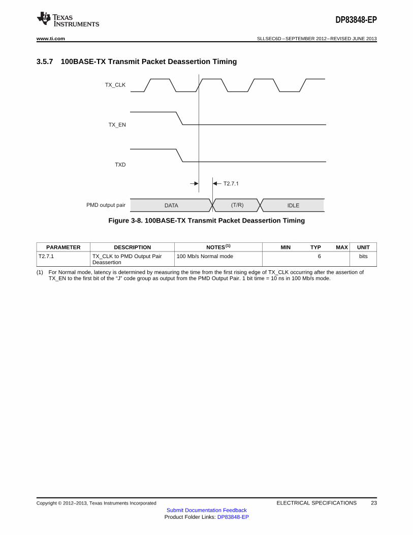
3.5.7 100BASE-TX Transmit Packet Deassertion Timing
Figure 3-8. 100BASE-TX Transmit Packet Deassertion Timing
xxxPARAMETER DESCRIPTION NOTES (1) MIN TYP MAX UNIT
T2.7.1 TX_CLK to PMD Output Pair 100 Mb/s Normal mode 6 bitsDeassertion
(1) For Normal mode, latency is determined by measuring the time from the first rising edge of TX_CLK occurring after the assertion ofTX_EN to the first bit of the “J” code group as output from the PMD Output Pair. 1 bit time = 10 ns in 100 Mb/s mode.
Copyright © 2012–2013, Texas Instruments Incorporated ELECTRICAL SPECIFICATIONS 23Submit Documentation Feedback
Product Folder Links: DP83848-EP

PMD output pair
T2.8.1
T2.8.1T2.8.1
T2.8.1
+1 rise
+1 fall
–1 fall –1 rise
eye pattern
T2.8.2
T2.8.2
90%
10%
10%
90%
PMD output pair
DP83848-EP
SLLSEC6D –SEPTEMBER 2012–REVISED JUNE 2013 www.ti.com
3.5.8 100BASE-TX Transmit Timing (tR/F & Jitter)
Figure 3-9. 100BASE-TX Transmit Timing (tR/F & Jitter)
xxxPARAMETER DESCRIPTION NOTES (1) (2) MIN TYP MAX UNIT
T2.8.1 100 Mb/s PMD Output Pair tR and tF 2.6 4 5.5 ns
100 Mb/s tR and tF Mismatch 500 ps
T2.8.2 (3) 100 Mb/s PMD Output Pair Transmit 1.4 nsJitter
(1) Normal Mismatch is the difference between the maximum and minimum of all rise and fall times.(2) Rise and fall times taken at 10% and 90% of the +1 or -1 amplitude.(3) Specified from -40°C to 125°C.
24 ELECTRICAL SPECIFICATIONS Copyright © 2012–2013, Texas Instruments Incorporated
Submit Documentation FeedbackProduct Folder Links: DP83848-EP

(T/R) IDLEDATAPMD input pair
CRS
T2.10.1
(J/K)IDLE DATAPMD input pair
CRS
RXD[3:0]RX_DVRX_ER
T2.9.1
T2.9.2
DP83848-EP
www.ti.com SLLSEC6D –SEPTEMBER 2012–REVISED JUNE 2013
3.5.9 100BASE-TX Receive Packet Latency Timing
Figure 3-10. 100BASE-TX Receive Packet Latency Timing
xxxPARAMETER DESCRIPTION (1) NOTES (2) (3) MIN TYP MAX UNIT
T2.9.1 Carrier Sense ON Delay 100 Mb/s Normal mode 20 bits
T2.9.2 Receive Data Latency 100 Mb/s Normal mode 24 bits
(1) Carrier Sense On Delay is determined by measuring the time from the first bit of the “J” code group to the assertion of Carrier Sense.(2) 1 bit time = 10 ns in 100 Mb/s mode.(3) PMD Input Pair voltage amplitude is greater than the Signal Detect Turn-On Threshold Value.
3.5.10 100BASE-TX Receive Packet Deassertion Timing
Figure 3-11. 100BASE-TX Receive Packet Deassertion Timing
xxxPARAMETER DESCRIPTION NOTES (1) (2) MIN TYP MAX UNIT
T2.10.1 Carrier Sense OFF Delay 100 Mb/s Normal mode 24 bits
(1) Carrier Sense Off Delay is determined by measuring the time from the first bit of the “T” code group to the deassertion of Carrier Sense.(2) 1 bit time = 10 ns in 100 Mb/s mode
Copyright © 2012–2013, Texas Instruments Incorporated ELECTRICAL SPECIFICATIONS 25Submit Documentation Feedback
Product Folder Links: DP83848-EP

RX_CLK
RXD[3:0]
RX_DVValid data
T2.12.2T2.12.3
T2.12.1 T2.12.1
TX_CLK
TXD[3:0]TX_EN Valid data
T2.11.1 T2.11.1
T2.11.2 T211.3
DP83848-EP
SLLSEC6D –SEPTEMBER 2012–REVISED JUNE 2013 www.ti.com
3.5.11 10 Mb/s MII Transmit Timing
Figure 3-12. 10 Mb/s MII Transmit Timing
xxxPARAMETER DESCRIPTION NOTES (1) MIN TYP MAX UNIT
T2.11.1 TX_CLK High/Low Time 10 Mb/s MII mode 190 200 210 ns
T2.11.2 TXD[3:0], TX_EN Data Setup to 10 Mb/s MII mode 24.70 nsTX_CLK fall
T2.11.3 TXD[3:0], TX_EN Data Hold from 10 Mb/s MII mode 0 nsTX_CLK rise
(1) An attached Mac should drive the transmit signals using the positive edge of TX_CLK. As shown above, the MII signals are sampled onthe falling edge of TX_CLK.
3.5.12 10 Mb/s MII Receive Timing
Figure 3-13. 10 Mb/s MII Receive Timing
xxxPARAMETER DESCRIPTION NOTES (1) MIN TYP MAX UNIT
T2.12.1 RX_CLK High/Low Time 160 200 240 ns
T2.12.2 RX_CLK to RXD[3:0], RX_DV 10 Mb/s MII mode 100 nsDelay
T2.12.3 RX_CLK rising edge delay from 10 Mb/s MII mode 100 nsRXD[3:0], RX_DV Valid
(1) RX_CLK may be held low for a longer period of time during transition between reference and recovered clocks. Minimum high and lowtimes will not be violated.
26 ELECTRICAL SPECIFICATIONS Copyright © 2012–2013, Texas Instruments Incorporated
Submit Documentation FeedbackProduct Folder Links: DP83848-EP

RX_CLK
RXD[0]
RX_DVValid data
T2.14.2
T2.14.1 T2.14.1
TX_CLK
TXD[0]TX_EN Valid data
T2.13.1 T2.13.2
T2.13.3 T2.13.4
DP83848-EP
www.ti.com SLLSEC6D –SEPTEMBER 2012–REVISED JUNE 2013
3.5.13 10 Mb/s Serial Mode Transmit Timing
Figure 3-14. 10 Mb/s Serial Mode Transmit Timing
xxxPARAMETER DESCRIPTION NOTES MIN TYP MAX UNIT
T2.13.1 TX_CLK High Time 10 Mb/s Serial mode 20 25 30 ns
T2.13.2 TX_CLK Low Time 10 Mb/s Serial mode 70 75 80 ns
T2.13.3 TXD_0, TX_EN Data Setup to 10 Mb/s Serial mode 24.70 nsTX_CLK rise
T2.13.4 TXD_0, TX_EN Data Hold from 10 Mb/s Serial mode 0 nsTX_CLK rise
3.5.14 10 Mb/s Serial Mode Receive Timing
Figure 3-15. 10 Mb/s Serial Mode Receive Timing
xxxPARAMETER DESCRIPTION NOTES (1) MIN TYP MAX UNIT
T2.14.1 RX_CLK High/Low Time 35 50 65 ns
T2.14.2 RX_CLK fall to RXD_0, RX_DV 10 Mb/s Serial mode -10 10 nsDelay
(1) RX_CLK may be held high for a longer period of time during transition between reference and recovered clocks. Minimum high and lowtimes will not be violated.
Copyright © 2012–2013, Texas Instruments Incorporated ELECTRICAL SPECIFICATIONS 27Submit Documentation Feedback
Product Folder Links: DP83848-EP

TX_CLK
TX_EN
PWD output pair
PMD output pair
0 0 T2.16.1
T2.16.2
1 1
TX_CLK
TX_EN
TXD
PMD output pair
T2.15.2
T2.15.1
DP83848-EP
SLLSEC6D –SEPTEMBER 2012–REVISED JUNE 2013 www.ti.com
3.5.15 10BASE-T Transmit Timing (Start of Packet)
Figure 3-16. 10BASE-T Transmit Timing (Start of Packet)
xxxPARAMETER DESCRIPTION NOTES MIN TYP MAX UNIT
T2.15.1 Transmit Output Delay from the 10 Mb/s MII mode 3.5 bitsFalling Edge of TX_CLK
T2.15.2 Transmit Output Delay from the 10 Mb/s Serial mode 3.5 bitsRising Edge of TX_CLK
3.5.16 10BASE-T Transmit Timing (End of Packet)
Figure 3-17. 10BASE-T Transmit Timing (End of Packet)
xxxPARAMETER DESCRIPTION NOTES MIN TYP MAX UNIT
T2.16.1 End of Packet High Time (with ‘0’ 250 300 nsending bit)
T2.16.2 End of Packet High Time (with ‘1’ 250 300 nsending bit)
28 ELECTRICAL SPECIFICATIONS Copyright © 2012–2013, Texas Instruments Incorporated
Submit Documentation FeedbackProduct Folder Links: DP83848-EP

1 0 1
PMD input pair
RX_CLK
CRS
IDLE
T2.18.1
First SFD bit decoded
1 0 1 0 1 0 101011
TPRD±
CRS
T2.17.1
T2.17.2
0000
T2.17.3
Preamble SFD Data
RX_CLK
RX_DV
RXD[3:0]
DP83848-EP
www.ti.com SLLSEC6D –SEPTEMBER 2012–REVISED JUNE 2013
3.5.17 10BASE-T Receive Timing (Start of Packet)
Figure 3-18. 10BASE-T Receive Timing (Start of Packet)
xxxPARAMETER DESCRIPTION NOTES (1) (2) MIN TYP MAX UNIT
T2.17.1 Carrier Sense Turn On Delay (PMD 630 1000 nsInput Pair to CRS)
T2.17.2 RX_DV Latency 10 bits
T2.17.3 Receive Data Latency Measurement shown from SFD 8 bits
(1) 10BASE-T RX_DV Latency is measured from first bit of preamble on the wire to the assertion of RX_DV(2) 1 bit time = 100 ns in 10 Mb/s mode.
3.5.18 10BASE-T Receive Timing (End of Packet)
Figure 3-19. 10BASE-T Receive Timing (End of Packet)
xxxPARAMETER DESCRIPTION NOTES MIN TYP MAX UNIT
T2.18.1 Carrier Sense Turn Off Delay 1 µs
Copyright © 2012–2013, Texas Instruments Incorporated ELECTRICAL SPECIFICATIONS 29Submit Documentation Feedback
Product Folder Links: DP83848-EP

Normal link pulses
T2.21.1
T2.21.2
TXE
PMD output pair
COL
T2.20.1T2.20.2
TX_CLK
TX_EN
COL
T2.19.1 T2.19.2
DP83848-EP
SLLSEC6D –SEPTEMBER 2012–REVISED JUNE 2013 www.ti.com
3.5.19 10 Mb/s Heartbeat Timing
Figure 3-20. 10 Mb/s Heartbeat Timing
xxxPARAMETER DESCRIPTION NOTES MIN TYP MAX UNIT
T2.19.1 CD Heartbeat Delay All 10 Mb/s modes 1200 ns
T2.19.2 CD Heartbeat Duration All 10 Mb/s modes 1000 ns
3.5.20 10 Mb/s Jabber Timing
Figure 3-21. 10 Mb/s Jabber Timing
xxxPARAMETER DESCRIPTION NOTES MIN TYP MAX UNIT
T2.20.1 Jabber Activation Time 85 ms
T2.20.2 Jabber Deactivation Time 500 ms
3.5.21 10BASE-T Normal Link Pulse Timing
Figure 3-22. 10BASE-T Normal Link Pulse Timing
xxxPARAMETER DESCRIPTION NOTES (1) MIN TYP MAX UNIT
T2.21.1 Pulse Width 100 ns
T2.21.2 Pulse Period 16 ms
(1) These specifications represent transmit timings.
30 ELECTRICAL SPECIFICATIONS Copyright © 2012–2013, Texas Instruments Incorporated
Submit Documentation FeedbackProduct Folder Links: DP83848-EP

SD+ internal
PMD Input Pair
T2.23.1T2.23.2
Fast link pulses
T2.22.1
T2.22.3
T2.22.2
T2.22.1
T2.22.5
T2.22.4
clockpulse
clockpulse
datapulse
FLP burst FLP burst
DP83848-EP
www.ti.com SLLSEC6D –SEPTEMBER 2012–REVISED JUNE 2013
3.5.22 Auto-Negotiation Fast Link Pulse (FLP) Timing
Figure 3-23. Auto-Negotiation Fast Link Pulse (FLP) Timing
xxxPARAMETER DESCRIPTION NOTES MIN TYP MAX UNIT
T2.22.1 Clock, Data Pulse Width 100 ns
T2.22.2 Clock Pulse to Clock Pulse Period 125 μs
T2.22.3 Clock Pulse to Data Pulse Period Data = 1 62 μs
T2.22.4 Burst Width 2 ms
T2.22.5 FLP Burst to FLP Burst Period 16 ms
3.5.23 100BASE-TX Signal Detect Timing
Figure 3-24. 100BASE-TX Signal Detect Timing
xxxPARAMETER DESCRIPTION NOTES (1) MIN TYP MAX UNIT
T2.23.1 SD Internal Turn-on Time 1 ms
T2.23.2 SD Internal Turn-off Time 350 µs
(1) The signal amplitude on PMD Input Pair must be TP-PMD compliant.
Copyright © 2012–2013, Texas Instruments Incorporated ELECTRICAL SPECIFICATIONS 31Submit Documentation Feedback
Product Folder Links: DP83848-EP
TX_CLK
TX_EN
TXD[3:0]
CRS
RX_CLK
RXD[3:0]
RX_DV
T2.24.1
DP83848-EP
SLLSEC6D –SEPTEMBER 2012–REVISED JUNE 2013 www.ti.com
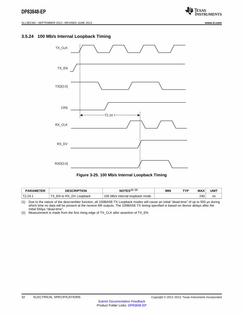
3.5.24 100 Mb/s Internal Loopback Timing
Figure 3-25. 100 Mb/s Internal Loopback Timing
xxxPARAMETER DESCRIPTION NOTES (1) (2) MIN TYP MAX UNIT
T2.24.1 TX_EN to RX_DV Loopback 100 Mb/s internal loopback mode 240 ns
(1) Due to the nature of the descrambler function, all 100BASE-TX Loopback modes will cause an initial “dead-time” of up to 550 μs duringwhich time no data will be present at the receive MII outputs. The 100BASE-TX timing specified is based on device delays after theinitial 550μs “dead-time”.
(2) Measurement is made from the first rising edge of TX_CLK after assertion of TX_EN.
32 ELECTRICAL SPECIFICATIONS Copyright © 2012–2013, Texas Instruments Incorporated
Submit Documentation FeedbackProduct Folder Links: DP83848-EP

TX_CLK
TX_EN
TXD[3:0]
CRS
RX_CLK
RXD[3:0]
RX_DV
T2.25.1
DP83848-EP
www.ti.com SLLSEC6D –SEPTEMBER 2012–REVISED JUNE 2013
3.5.25 10 Mb/s Internal Loopback Timing
Figure 3-26. 10 Mb/s Internal Loopback Timing
xxxPARAMETER DESCRIPTION NOTES (1) MIN TYP MAX UNIT
T2.25.1 TX_EN to RX_DV Loopback 10 Mb/s internal loopback mode 2 µs
(1) Measurement is made from the first rising edge of TX_CLK after assertion of TX_EN.
Copyright © 2012–2013, Texas Instruments Incorporated ELECTRICAL SPECIFICATIONS 33Submit Documentation Feedback
Product Folder Links: DP83848-EP
X1
TXD[1:0]TX_EN Valid data
PMD output pair Symbol
T2.26.1
T2.26.4
T2.26.2 T2.26.3
DP83848-EP
SLLSEC6D –SEPTEMBER 2012–REVISED JUNE 2013 www.ti.com
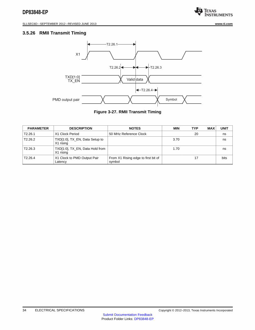
3.5.26 RMII Transmit Timing
Figure 3-27. RMII Transmit Timing
xxxPARAMETER DESCRIPTION NOTES MIN TYP MAX UNIT
T2.26.1 X1 Clock Period 50 MHz Reference Clock 20 ns
T2.26.2 TXD[1:0], TX_EN, Data Setup to 3.70 nsX1 rising
T2.26.3 TXD[1:0], TX_EN, Data Hold from 1.70 nsX1 rising
T2.26.4 X1 Clock to PMD Output Pair From X1 Rising edge to first bit of 17 bitsLatency symbol
34 ELECTRICAL SPECIFICATIONS Copyright © 2012–2013, Texas Instruments Incorporated
Submit Documentation FeedbackProduct Folder Links: DP83848-EP

CRS_DV
X1
RXD[1:0]
RX_ER
T2.27.2
T2.27.1
T2.27.2
PMD Input Pair
T2.27.3
T2.27.5
RX_DV
T2.27.2 T2.27.2
IDLE (J/K) Data (TR) Data
T2.27.4
DP83848-EP
www.ti.com SLLSEC6D –SEPTEMBER 2012–REVISED JUNE 2013
3.5.27 RMII Receive Timing
Figure 3-28. RMII Receive Timing
xxxPARAMETER DESCRIPTION NOTES (1) (2) (3) MIN TYP MAX UNIT
T2.27.1 X1 Clock Period 50 MHz Reference Clock 20 ns
T2.27.2 RXD[1:0], CRS_DV, RX_DV and 2 14 nsRX_ER output delay from X1 rising
T2.27.3 CRS ON delay From JK symbol on PMD 18.5 bitsReceive Pair to initial assertionof CRS_DV
T2.27.4 CRS OFF delay From TR symbol on PMD 27 bitsReceive Pair to initialdeassertion of CRS_DV
T2.27.5 RXD[1:0] and RX_ER latency From symbol on Receive Pair. 38 bitsElasticity buffer set to defaultvalue (01).
(1) Per the RMII Specification, output delays assume a 25pF load.(2) CRS_DV is asserted asynchronously in order to minimize latency of control signals through the why. CRS_DV may toggle
synchronously at the end of the packet to indicate CRS deassertion.(3) RX_DV is synchronous to X1. While not part of the RMII specification, this signal is provided to simplify recovery of receive data.
Copyright © 2012–2013, Texas Instruments Incorporated ELECTRICAL SPECIFICATIONS 35Submit Documentation Feedback
Product Folder Links: DP83848-EP

X1
25 MHz_OUT
T2.29.2
T2.29.1T2.29.1
Clear bit 10 of BMCR(return to normal operation
from Isolate mode)
Hardware or Software Reset
(with PHYAD 00000)¹
MODE
T2.28.1
T2.28.2
ISOLATE NORMAL
DP83848-EP
SLLSEC6D –SEPTEMBER 2012–REVISED JUNE 2013 www.ti.com
3.5.28 Isolation Timing
Figure 3-29. Isolation Timing
xxxPARAMETER DESCRIPTION NOTES MIN TYP MAX UNIT
T2.28.1 From software clear of bit 10 in the 100 µsBMCR register to the transition fromIsolate to Normal Mode
T2.28.2 From Deassertion of S/W or H/W Reset 500 µsto transition from Isolate to Normalmode
3.5.29 25 MHz_OUT Timing
Figure 3-30. 25 MHz_OUT Timing
xxxPARAMETER DESCRIPTION NOTES (1) MIN TYP MAX UNIT
MII mode 20T2.29.1 25 MHz_OUT High/Low Time ns
RMII mode 10
T2.29.2 25 MHz_OUT propagation delay Relative to X1 8 ns
(1) 25 MHz_OUT characteristics are dependent upon the X1 input characteristics.
36 ELECTRICAL SPECIFICATIONS Copyright © 2012–2013, Texas Instruments Incorporated
Submit Documentation FeedbackProduct Folder Links: DP83848-EP
DP83848-EP
www.ti.com SLLSEC6D –SEPTEMBER 2012–REVISED JUNE 2013
4 CONFIGURATION
4.1 Auto-Negotiation
The auto-negotiation function provides a mechanism for exchanging configuration information betweentwo ends of a link segment and automatically selecting the highest performance mode of operationsupported by both devices. Fast link pulse (FLP) bursts provide the signalling used to communicate auto-negotiation abilities between two devices at each end of a link segment. For further detail regarding auto-negotiation, refer to Clause 28 of the IEEE 802.3u specification. The DP83848 supports four differentethernet protocols (10 Mb/s half duplex, 10 Mb/s full duplex, 100 Mb/s half duplex, and 100 Mb/s fullduplex), so the inclusion of auto-negotiation ensures that the highest performance protocol will be selectedbased on the advertised ability of the link partner. The auto-negotiation function within the DP83848 canbe controlled either by internal register access or by the use of the AN_EN, AN1 and AN0 pins.
4.1.1 Auto-Negotiation Pin Control
The state of AN_EN, AN0 and AN1 determines whether the DP83848 is forced into a specific mode orauto-negotiation will advertise a specific ability (or set of abilities) as given in Table 4-1. These pins allowconfiguration options to be selected without requiring internal register access.
The state of AN_EN, AN0 and AN1, upon power-up/reset, determines the state of bits [8:5] of the ANARregister.
The auto-negotiation function selected at power-up or reset can be changed at any time by writing to thebasic mode control register (BMCR) at address 0x00h.
Table 4-1. Auto-Negotiation Modes
AN_EN AN1 AN0 Forced Mode
0 0 0 10BASE-T, Half Duplex
0 0 1 10BASE-T, Full Duplex
0 1 0 100BASE-TX, Half Duplex
0 1 1 100BASE-TX, Full Duplex
AN_EN AN1 AN0 Advertised Mode
1 0 0 10BASE-T, Half or Full Duplex
1 0 1 100BASE-TX, Half or Full Duplex
10BASE-T Half Duplex1 1 0 100BASE-TX, Half Duplex
10BASE-T, Half/Full Duplex1 1 1 100BASE-TX, Half/Full Duplex
4.1.2 Auto-Negotiation Register Control
When auto-negotiation is enabled, the DP83848 transmits the abilities programmed into the auto-negotiation advertisement register (ANAR) at address 04h via FLP Bursts. Any combination of 10 Mb/s,100 Mb/s, half duplex, and full duplex modes may be selected.
Auto-negotiation priority resolution:
1. 100BASE-TX Full Duplex (Highest Priority)
2. 100BASE-TX Half Duplex
3. 10BASE-T Full Duplex
4. 10BASE-T Half Duplex (Lowest Priority)
Copyright © 2012–2013, Texas Instruments Incorporated CONFIGURATION 37Submit Documentation Feedback
Product Folder Links: DP83848-EP

DP83848-EP
SLLSEC6D –SEPTEMBER 2012–REVISED JUNE 2013 www.ti.com
The basic mode control register (BMCR) at address 00h provides control for enabling, disabling, andrestarting the auto-negotiation process. When auto-negotiation is disabled, the speed selection bit in theBMCR controls switching between 10 Mb/s or 100 Mb/s operation, and the duplex mode bit controlsswitching between full duplex operation and half duplex operation. The speed selection and duplex modebits have no effect on the mode of operation when the auto-negotiation enable bit is set.
The link speed can be examined through the PHY status register (PHYSTS) at address 10h after a Link isachieved.
The BMSR indicates the set of available abilities for technology types, auto-negotiation ability, andextended register capability. These bits are permanently set to indicate the full functionality of theDP83848 (only the 100BASE-T4 bit is not set since the DP83848 does not support that function).
The BMSR also provides status on:• Whether or not auto-negotiation is complete• Whether or not the Link Partner is advertising that a remote fault has occurred• Whether or not valid link has been established• Support for management frame preamble suppression
The ANAR indicates the auto-negotiation abilities to be advertised by the DP83848. All available abilitiesare transmitted by default, but any ability can be suppressed by writing to the ANAR. Updating the ANARto suppress an ability is one way for a management agent to change (restrict) the technology that is used.
The auto-negotiation link partner ability register (ANLPAR) at address 05h is used to receive the base linkcode word as well as all next page code words during the negotiation. Furthermore, the ANLPAR will beupdated to either 0081h or 0021h for parallel detection to either 100 Mb/s or 10 Mb/s respectively.
The auto-negotiation expansion register (ANER) indicates additional auto-negotiation status. The ANERprovides status on:• Whether or not a parallel detect fault has occurred• Whether or not the link partner supports the next page function• Whether or not the DP83848 supports the next page function• Whether or not the current page being exchanged by auto-negotiation has been received• Whether or not the link partner supports auto negotiation
4.1.3 Auto-Negotiation Parallel Detection
The DP83848 supports the parallel detection function as defined in the IEEE 802.3u specification. Paralleldetection requires both the 10 Mb/s and 100 Mb/s receivers to monitor the receive signal and report linkstatus to the auto-negotiation function. Auto-negotiation uses this information to configure the correcttechnology in the event that the link partner does not support auto-negotiation but is transmitting linksignals that the 100BASE-TX or 10BASET PMAs recognize as valid link signals.
If the DP83848 completes auto-negotiation as a result of parallel detection, bits 5 and 7 within theANLPAR register will be set to reflect the mode of operation present in the link partner. Note that bits 4:0of the ANLPAR will also be set to 00001 based on a successful parallel detection to indicate a valid 802.3selector field. Software may determine that negotiation completed via parallel detection by reading a zeroin the link partner auto-negotiation able bit once the auto-negotiation complete bit is set. If configured forparallel detect mode and any condition other than a single good link occurs then the parallel detect faultbit will be set.
4.1.4 Auto-Negotiation Restart
Once auto-negotiation has completed, it may be restarted at any time by setting bit 9 (restart auto-negotiation) of the BMCR to one. If the mode configured by a successful auto-negotiation loses a validlink, then the auto-negotiation process will resume and attempt to determine the configuration for the link.This function ensures that a valid configuration is maintained if the cable becomes disconnected.
38 CONFIGURATION Copyright © 2012–2013, Texas Instruments Incorporated
Submit Documentation FeedbackProduct Folder Links: DP83848-EP

DP83848-EP
www.ti.com SLLSEC6D –SEPTEMBER 2012–REVISED JUNE 2013
A renegotiation request from any entity, such as a management agent, will cause the DP83848 to halt anytransmit data and link pulse activity until the break_link_timer expires (~1500 ms). Consequently, the linkpartner will go into link fail and normal auto-negotiation resumes. The DP83848 will resume auto-negotiation after the break_link_timer has expired by issuing FLP bursts.
4.1.5 Enabling Auto-Negotiation via Software
It is important to note that if the DP83848 has been initialized upon power-up as a non-auto-negotiatingdevice (forced technology), and it is then required that auto-negotiation or re-auto-negotiation be initiatedvia software, bit 12 (auto-negotiation enable) of the BMCR must first be cleared and then set for any auto-negotiation function to take effect.
4.1.6 Auto-Negotiation Complete Time
Parallel detection and auto-negotiation take approximately 2-3 seconds to complete. In addition, auto-negotiation with next page should take approximately 2-3 seconds to complete, depending on the numberof next pages sent.
Refer to Clause 28 of the IEEE 802.3u standard for a full description of the individual timers related toauto-negotiation.
4.2 Auto-MDIX
When enabled, this function utilizes auto-negotiation to determine the proper configuration for transmissionand reception of data and subsequently selects the appropriate MDI pair for MDI/MDIX operation. Thefunction uses a random seed to control switching of the crossover circuitry. This implementation complieswith the corresponding IEEE 802.3 auto-negotiation and crossover specifications.
Auto-MDIX is enabled by default and can be configured via strap or via PHYCR (0x19h) register, bits[15:14].
Neither auto-negotiation nor auto-MDIX is required to be enabled in forcing crossover of the MDI pairs.Forced crossover can be achieved through the FORCE_MDIX bit, bit 14 of PHYCR (0x19h) register.
NOTEAuto-MDIX will not work in a forced mode of operation.
4.3 PHY Address
The 5 PHY address inputs pins are shared with the RXD[3:0] pins and COL pin as shown below.
Table 4-2. PHY Address Mapping
PIN NUMBER PHYAD FUNCTION RXD FUNCTION
42 PHYAD0 COL
43 PHYAD1 RXD_0
44 PHYAD2 RXD_1
45 PHYAD3 RXD_2
46 PHYAD4 RXD_3
Copyright © 2012–2013, Texas Instruments Incorporated CONFIGURATION 39Submit Documentation Feedback
Product Folder Links: DP83848-EP

CO
L
RX
D_0
RX
D_1
RX
D_
2
RX
D_
3
VCC
2.2
kΩ
PHYAD0 = 1PHYAD1 = 1PHYAD2 = 0PHYAD3 = 0PHYAD4 = 0
DP83848-EP
SLLSEC6D –SEPTEMBER 2012–REVISED JUNE 2013 www.ti.com
The DP83848 can be set to respond to any of 32 possible PHY addresses via strap pins. The informationis latched into the PHYCR (address 19h, bits [4:0]) at device power-up and hardware reset. The PHYaddress pins are shared with the RXD and COL pins. Each DP83848 or port sharing an MDIO bus in asystem must have a unique physical address.
The DP83848 supports PHY address strapping values 0 (<00000>) through 31 (<11111>). Strapping PHYaddress 0 puts the part into isolate mode. It should also be noted that selecting PHY address 0 via anMDIO write to PHYCR will not put the device in isolate mode.
For further detail relating to the latch-in timing requirements of the PHY address pins, as well as the otherhardware configuration pins, refer to the Reset summary in Section 8.
Since the PHYAD[0] pin has weak internal pull-up resistor and PHYAD[4:1] pins have weak internal pull-down resistors, the default setting for the PHY address is 00001 (01h).
Refer to Figure 4-1 for an example of a PHYAD connection to external components. In this example, thePHYAD strapping results in address 00011 (03h).
Figure 4-1. PHYAD Strapping Example
4.3.1 MII Isolate Mode
The DP83848 can be put into MII isolate mode by writing to bit 10 of the BMCR register or by strapping inphysical address 0. It should be noted that selecting physical address 0 via an MDIO write to PHYCR willnot put the device in the MII isolate mode.
When in the MII isolate mode, the DP83848 does not respond to packet data present at TXD[3:0], TX_ENinputs and presents a high impedance on the TX_CLK, RX_CLK, RX_DV, RX_ER, RXD[3:0], COL, andCRS outputs. When in Isolate mode, the DP83848 will continue to respond to all managementtransactions.
While in Isolate mode, the PMD output pair will not transmit packet data but will continue to source100BASE-TX scrambled idles or 10BASE-T normal link pulses.
The DP83848 can auto-negotiate or parallel detect to a specific technology depending on the receivesignal at the PMD input pair. A valid link can be established for the receiver even when the DP83848 is inIsolate mode.
4.4 LED Interface
The DP83848 supports three configurable light emitting diode (LED) pins. The device supports three LEDconfigurations: Link, Speed, Activity and Collision. Functions are multiplexed among the LEDs. ThePHYCR for the LEDs can also be selected through address 19h, bits [6:5].
40 CONFIGURATION Copyright © 2012–2013, Texas Instruments Incorporated
Submit Documentation FeedbackProduct Folder Links: DP83848-EP

DP83848-EP
www.ti.com SLLSEC6D –SEPTEMBER 2012–REVISED JUNE 2013
Table 4-3. LED Mode Select
LED_CFG[0]LED_CGF[1]MODE (BIT 5) LED_LINK LED_SPEED LED_ACT/COL(BIT 6) or (PIN 40)
ON for Good Link ON in 100 Mb/s ON for Activity1 don't care 1 OFF for No Link OFF in 10 Mb/s OFF for No Activity
ON for Good Link ON in 100 Mb/s ON for Collision2 0 0 BLINK for Activity OFF in 10 Mb/s OFF for No Collision
ON for Good Link ON in 100 Mb/s ON for Full Duplex3 1 0 BLINK for Activity OFF in 10 Mb/s OFF for Half Duplex
The LED_LINK pin in Mode 1 indicates the link status of the port. In 100BASE-T mode, link is establishedas a result of input receive amplitude compliant with the TPPMD specifications which will result in internalgeneration of signal detect. A 10 Mb/s Link is established as a result of the reception of at least sevenconsecutive normal link pulses or the reception of a valid 10BASE-T packet. This will cause the assertionof LED_LINK. LED_LINK will deassert in accordance with the Link Loss Timer as specified in the IEEE802.3 specification.
The LED_LINK pin in Mode 1 will be OFF when no LINK is present.
The LED_LINK pin in Mode 2 and Mode 3 will be ON to indicate Link is good and BLINK to indicateactivity is present on either transmit or receive activity.
The LED_SPEED pin indicates 10 or 100 Mb/s data rate of the port. The standard CMOS driver goes highwhen operating in 100 Mb/s operation. The functionality of this LED is independent of mode selected.
The LED_ACT/COL pin in Mode 1 indicates the presence of either transmit or receive activity. The LEDwill be ON for Activity and OFF for No Activity. In Mode 2, this pin indicates the Collision status of the port.The LED will be ON for Collision and OFF for No Collision.
The LED_ACT/COL pin in Mode 3 indicates the presence of duplex status for 10 Mb/s or 100 Mb/soperation. The LED will be ON for full duplex and OFF for half duplex.
In 10 Mb/s half duplex mode, the collision LED is based on the COL signal.
Since these LED pins are also used as strap options, the polarity of the LED is dependent on whether thepin is pulled up or down.
4.4.1 LEDs
Since the auto-negotiation (AN) strap options share the LED output pins, the external componentsrequired for strapping and LED usage must be considered in order to avoid contention.
Specifically, when the LED outputs are used to drive LEDs directly, the active state of each output driver isdependent on the logic level sampled by the corresponding AN input upon power-up/reset. For example, ifa given AN input is resistively pulled low then the corresponding output will be configured as an activehigh driver. Conversely, if a given AN input is resistively pulled high, then the corresponding output will beconfigured as an active low driver.
Refer to Figure 4-2 for an example of AN connections to external components. In this example, the ANstrapping results in auto-negotiation with 10/100 half or full duplex advertised.
The adaptive nature of the LED outputs helps to simplify potential implementation issues of these dualpurpose pins.
Copyright © 2012–2013, Texas Instruments Incorporated CONFIGURATION 41Submit Documentation Feedback
Product Folder Links: DP83848-EP

LE
D_
LIN
K
LE
D_
SP
EE
D
LE
D_A
CT
/CO
L
VCC
2.2
kΩ
110
Ω
110
Ω2.2
kΩ
110
Ω
AN0 = 1AN1 = 1AN_EN = 1
2.2
kΩ
DP83848-EP
SLLSEC6D –SEPTEMBER 2012–REVISED JUNE 2013 www.ti.com
Figure 4-2. AN Strapping and LED Loading Example
4.4.2 LED Direct Control
The DP83848 provides another option to directly control any or all LED outputs through the LED directcontrol register (LEDCR), address 18h. The register does not provide read access to LEDs.
4.5 Half Duplex vs Full Duplex
The DP83848 supports both half and full duplex operation at both 10 Mb/s and 100 Mb/s speeds.
Half duplex relies on the CSMA/CD protocol to handle collisions and network access. In half duplex mode,CRS responds to both transmit and receive activity in order to maintain compliance with the IEEE 802.3specification.
Since the DP83848 is designed to support simultaneous transmit and receive activity it is capable ofsupporting fullduplex switched applications with a throughput of up to 200 Mb/s per port when operating in100BASE-TX mode. Because the CSMA/CD protocol does not apply to fullduplex operation, the DP83848disables its own internal collision sensing and reporting functions and modifies the behavior of carriersense (CRS) such that it indicates only receive activity. This allows a full duplex capable MAC to operateproperly.
All modes of operation (100BASE-TX and 10BASE-T) can run either half duplex or full duplex.Additionally, other than CRS and collision reporting, all remaining MII signaling remains the sameregardless of the selected duplex mode.
It is important to understand that while auto-negotiation with the use of fast link pulse code words caninterpret and configure to full duplex operation, parallel detection can not recognize the difference betweenfull and half duplex from a fixed 10 Mb/s or 100 Mb/s link partner over twisted pair. As specified in the802.3u specification, if a far-end link partner is configured to a forced full duplex 100BASE-TX ability, theparallel detection state machine in the partner would be unable to detect the full duplex capability of thefar-end link partner. This link segment would negotiate to a half duplex 100BASE-TX configuration (samescenario for 10 Mb/s).
4.6 Internal Loopback
The DP83848 includes a loopback test mode for facilitating system diagnostics. The loopback mode isselected through bit 14 (loopback) of the BMCR. Writing 1 to this bit enables MII transmit data to be routedto the MII receive outputs. Loopback status may be checked in bit 3 of PHYSTS. While in Loopback modethe data will not be transmitted onto the media. To ensure that the desired operating mode is maintained,Auto-Negotiation should be disabled before selecting the loopback mode.
42 CONFIGURATION Copyright © 2012–2013, Texas Instruments Incorporated
Submit Documentation FeedbackProduct Folder Links: DP83848-EP
DP83848-EP
www.ti.com SLLSEC6D –SEPTEMBER 2012–REVISED JUNE 2013
4.7 BIST
The DP83848 incorporates an internal built-in self test (BIST) circuit to accommodate in-circuit testing ordiagnostics. The BIST circuit can be utilized to test the integrity of the transmit and receive data paths.BIST testing can be performed with the part in the internal loopback mode or externally looped back usinga loopback cable fixture.
The BIST is implemented with independent transmit and receive paths, with the transmit block generatinga continuous stream of a pseudo random sequence. The user can select a 9 bit or 15 bit pseudo randomsequence from the PSR_15 bit in the PHYCR. The received data is compared to the generated pseudo-random data by the BIST linear feedback shift register (LFSR) to determine the BIST pass or fail status.
The pass or fail status of the BIST is stored in the BIST status bit in the PHYCR register. The status bitdefaults to 0 (BIST fail) and will transition on a successful comparison. If an error (mis-compare) occurs,the status bit is latched and is cleared upon a subsequent write to the Start/Stop bit.
For transmit VOD testing, the packet BIST continuous mode can be used to allow continuous datatransmission, setting BIST_CONT_MODE, bit 5, of CDCTRL1 (0x1Bh).
The number of BIST errors can be monitored through the BIST error count in the CDCTRL1 (0x1Bh), bits[15:8].
Copyright © 2012–2013, Texas Instruments Incorporated CONFIGURATION 43Submit Documentation Feedback
Product Folder Links: DP83848-EP
DP83848-EP
SLLSEC6D –SEPTEMBER 2012–REVISED JUNE 2013 www.ti.com
5 FUNCTIONAL DESCRIPTION
The DP83848 supports several modes of operation using the MII interface pins. The options are defined inthe following sections and include:• MII mode• RMII mode• 10 Mb serial network interface (SNI)
The modes of operation can be selected by strap options or register control. For RMII mode, it is requiredto use the strap option, since it requires a 50 MHz clock instead of the normal 25 MHz.
In each of these modes, the IEEE 802.3 serial management interface is operational for deviceconfiguration and status. The serial management interface of the MII allows for the configuration andcontrol of multiple PHY devices, gathering of status, error information, and the determination of the typeand capabilities of the attached PHY(s).
5.1 MII Interface
The DP83848 incorporates the media independent interface (MII) as specified in Clause 22 of the IEEE802.3u standard. This interface may be used to connect PHY devices to a MAC in 10/100 Mb/s systems.This section describes the nibble wide MII data interface.
The nibble wide MII data interface consists of a receive bus and a transmit bus each with control signalsto facilitate data transfer between the PHY and the upper layer (MAC).
5.1.1 Nibble-Wide MII Data Interface
Clause 22 of the IEEE 802.3u specification defines the media independent Interface. This interfaceincludes a dedicated receive bus and a dedicated transmit bus. These two data buses, along with variouscontrol and status signals, allow for the simultaneous exchange of data between the DP83848 and theupper layer agent (MAC).
The receive interface consists of a nibble wide data bus RXD[3:0], a receive error signal RX_ER, a receivedata valid flag RX_DV, and a receive clock RX_CLK for synchronous transfer of the data. The receiveclock operates at either 2.5 MHz to support 10 Mb/s operation modes or at 25 MHz to support 100 Mb/soperational modes.
The transmit interface consists of a nibble wide data bus TXD[3:0], a transmit enable control signalTX_EN, and a transmit clock TX_CLK which runs at either 2.5 MHz or 25 MHz.
Additionally, the MII includes the carrier sense signal CRS, as well as a collision detect signal COL. TheCRS signal asserts to indicate the reception of data from the network or as a function of transmit data inhalf duplex mode. The COL signal asserts as an indication of a collision which can occur during halfduplex operation when both a transmit and receive operation occur simultaneously.
5.1.2 Collision Detect
For half duplex, a 10BASE-T or 100BASE-TX collision is detected when the receive and transmit channelsare active simultaneously. Collisions are reported by the COL signal on the MII.
If the DP83848 is transmitting in 10 Mb/s mode when a collision is detected, the collision is not reporteduntil seven bits have been received while in the collision state. This prevents a collision being reportedincorrectly due to noise on the network. The COL signal remains set for the duration of the collision.
If a collision occurs during a receive operation, it is immediately reported by the COL signal.
When heartbeat is enabled (only applicable to 10 Mb/s operation), approximately 1μs after thetransmission of each packet, a signal quality error (SQE) signal of approximately 10 bit times is generated(internally) to indicate successful transmission. SQE is reported as a pulse on the COL signal of the MII.
44 FUNCTIONAL DESCRIPTION Copyright © 2012–2013, Texas Instruments Incorporated
Submit Documentation FeedbackProduct Folder Links: DP83848-EP
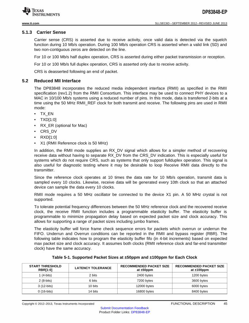
DP83848-EP
www.ti.com SLLSEC6D –SEPTEMBER 2012–REVISED JUNE 2013
5.1.3 Carrier Sense
Carrier sense (CRS) is asserted due to receive activity, once valid data is detected via the squelchfunction during 10 Mb/s operation. During 100 Mb/s operation CRS is asserted when a valid link (SD) andtwo non-contiguous zeros are detected on the line.
For 10 or 100 Mb/s half duplex operation, CRS is asserted during either packet transmission or reception.
For 10 or 100 Mb/s full duplex operation, CRS is asserted only due to receive activity.
CRS is deasserted following an end of packet.
5.2 Reduced MII Interface
The DP83848 incorporates the reduced media independent interface (RMII) as specified in the RMIIspecification (rev1.2) from the RMII Consortium. This interface may be used to connect PHY devices to aMAC in 10/100 Mb/s systems using a reduced number of pins. In this mode, data is transferred 2-bits at atime using the 50 MHz RMII_REF clock for both transmit and receive. The following pins are used in RMIImode:• TX_EN• TXD[1:0]• RX_ER (optional for Mac)• CRS_DV• RXD[1:0]• X1 (RMII Reference clock is 50 MHz)
In addition, the RMII mode supplies an RX_DV signal which allows for a simpler method of recoveringreceive data without having to separate RX_DV from the CRS_DV indication. This is especially useful forsystems which do not require CRS, such as systems that only support fullduplex operation. This signal isalso useful for diagnostic testing where it may be desirable to loop Receive RMII data directly to thetransmitter.
Since the reference clock operates at 10 times the data rate for 10 Mb/s operation, transmit data issampled every 10 clocks. Likewise, receive data will be generated every 10th clock so that an attacheddevice can sample the data every 10 clocks.
RMII mode requires a 50 MHz oscillator be connected to the device X1 pin. A 50 MHz crystal is notsupported.
To tolerate potential frequency differences between the 50 MHz reference clock and the recovered receiveclock, the receive RMII function includes a programmable elasticity buffer. The elasticity buffer isprogrammable to minimize propagation delay based on expected packet size and clock accuracy. Thisallows for supporting a range of packet sizes including jumbo frames.
The elasticity buffer will force frame check sequence errors for packets which overrun or underrun theFIFO. Underrun and Overrun conditions can be reported in the RMII and bypass register (RBR). Thefollowing table indicates how to program the elasticity buffer fifo (in 4-bit increments) based on expectedmax packet size and clock accuracy. It assumes both clocks (RMII reference clock and far-end transmitterclock) have the same accuracy.
Table 5-1. Supported Packet Sizes at ±50ppm and ±100ppm for Each Clock
START THRESHOLD RECOMMENDED PACKET SIZE RECOMMENDED PACKET SIZELATENCY TOLERANCERBR[1:0] at ±50ppm at ±100ppm
1 (4-bits) 2 bits 2400 bytes 1200 bytes
2 (8-bits) 6 bits 7200 bytes 3600 bytes
3 (12-bits) 10 bits 12000 bytes 6000 bytes
0 (16-bits) 14 bits 16800 bytes 8400 bytes
Copyright © 2012–2013, Texas Instruments Incorporated FUNCTIONAL DESCRIPTION 45Submit Documentation Feedback
Product Folder Links: DP83848-EP

DP83848-EP
SLLSEC6D –SEPTEMBER 2012–REVISED JUNE 2013 www.ti.com
5.3 10 Mb Serial Network Interface (SNI)
The DP83848 incorporates a 10 Mb serial network interface (SNI) which allows a simple serial datainterface for 10 Mb only devices. This is also referred to as a 7-wire interface. While there is no definedstandard for this interface, it is based on early 10 Mb physical layer devices. Data is clocked serially at10 MHz using separate transmit and receive paths. The following pins are used in SNI mode:• TX_CLK• TX_EN• TXD[0]• RX_CLK• RXD[0]• CRS• COL
5.4 802.3u MII Serial Management Interface
5.4.1 Serial Management Register Access
The serial management MII specification defines a set of thirty-two 16-bit status and control registers thatare accessible through the management interface pins MDC and MDIO. The DP83848 implements all therequired MII registers as well as several optional registers. A description of the serial management accessprotocol follows.
5.4.2 Serial Management Access Protocol
The serial control interface consists of two pins, management data clock (MDC) and management datainput/output (MDIO). MDC has a maximum clock rate of 25 MHz and no minimum rate. The MDIO line isbi-directional and may be shared by up to 32 devices. The MDIO frame format is shown below inTable 5-2.
The MDIO pin requires a pull-up resistor (1.5 kΩ) which, during IDLE and turnaround, will pull MDIO high.In order to initialize the MDIO interface, the station management entity sends a sequence of 32 contiguouslogic ones on MDIO to provide the DP83848 with a sequence that can be used to establishsynchronization. This preamble may be generated either by driving MDIO high for 32 consecutive MDCclock cycles, or by simply allowing the MDIO pull-up resistor to pull the MDIO pin high during which time32 MDC clock cycles are provided. In addition 32 MDC clock cycles should be used to re-sync the deviceif an invalid start, opcode, or turnaround bit is detected.
The DP83848 waits until it has received this preamble sequence before responding to any othertransaction. Once the DP83848 serial management port has been initialized no further preamblesequencing is required until after a power-on/reset, invalid start, invalid opcode, or invalid turnaround bithas occurred.
The start code is indicated by a <01> pattern. This assures the MDIO line transitions from the default idleline state.
Turnaround is defined as an idle bit time inserted between the register address field and the data field. Toavoid contention during a read transaction, no device shall actively drive the MDIO signal during the firstbit of turnaround. The addressed DP83848 drives the MDIO with a zero for the second bit of turnaroundand follows this with the required data. Figure 5-1 shows the timing relationship between MDC and theMDIO as driven or received by the station (STA) and the DP83848 (PHY) for a typical register readaccess.
For write transactions, the station management entity writes data to the addressed DP83848 thuseliminating the requirement for MDIO turnaround. The turnaround time is filled by the management entityby inserting <10>. Figure 5-2 shows the timing relationship for a typical MII register write access.
46 FUNCTIONAL DESCRIPTION Copyright © 2012–2013, Texas Instruments Incorporated
Submit Documentation FeedbackProduct Folder Links: DP83848-EP

MDC
MDIO(STA)
Idle StartOpcode(Write)
PHY Address(PHYAD = 0Ch)
Register Address(00h = BMCR)
TA Register Data Idle
z
z 0 1 0 1 0 1 1 10 0 0 0 0 0 0 0 0 0 0 0 0 0 0 0 0 0 0 0 0 0 0 0
z
z
MDC
MDIO(STA)
Idle StartOpcode(Read)
PHY Address(PHYAD = 0Ch)
Register Address(00h = BMCR)
TA Register Data
z
MDIO(PHY)
z
z
Idle
z
z
z z0 1 01 0 1 1 0 0 0 0 0 0 0 0 0 0 0 0 01 1 1 0 0 0 0 0 0 0 0
DP83848-EP
www.ti.com SLLSEC6D –SEPTEMBER 2012–REVISED JUNE 2013
Table 5-2. Typical MDIO Frame Format
MII MANAGEMENT SERIAL <idle><start><op code><device addr><reg addr><turnaround><data><idle>PROTOCOL
Read Operation <idle><01><10><AAAAA><RRRRR><Z0><xxxx xxxx xxxx xxxx><idle>
Write Operation <idle><01><01><AAAAA><RRRRR><10><xxxx xxxx xxxx xxxx><idle>
Figure 5-1. Typical MDC/MDIO Read Operation
Figure 5-2. Typical MDC/MDIO Write Operation
5.4.3 Serial Management Preamble Suppression
The DP83848 supports a preamble suppression mode as indicated by a one in bit 6 of the basic modestatus register (BMSR, address 01h.) If the station management entity (i.e. MAC or other managementcontroller) determines that all PHYs in the system support preamble suppression by returning a one in thisbit, then the station management entity need not generate preamble for each management transaction.
The DP83848 requires a single initialization sequence of 32 bits of preamble following hardware/softwarereset.
This requirement is generally met by the mandatory pull-up resistor on MDIO in conjunction with acontinuous MDC, or the management access made to determine whether preamble suppression issupported.
While the DP83848 requires an initial preamble sequence of 32 bits for management initialization, it doesnot require a full 32-bit sequence between each subsequent transaction. A minimum of one idle bitbetween management transactions is required as specified in the IEEE 802.3u specification.
Copyright © 2012–2013, Texas Instruments Incorporated FUNCTIONAL DESCRIPTION 47Submit Documentation Feedback
Product Folder Links: DP83848-EP

Scrambler
PMD OUTPUT PAIR
TX_CLK
125-MHZ Clock
BP_SCR MUX
MLT[1:0]
Divide by 54B5B Code
Croup Encoder
5B Parallelto Serial
NRZ to NRZIEncoder
Binary to MLT-3 /Common Driver
100Base-TXLoopback
TXD[3:0] /TX_EN
DP83848-EP
SLLSEC6D –SEPTEMBER 2012–REVISED JUNE 2013 www.ti.com
6 ARCHITECTURE
6.1 100BASE-TX Transmitter
The 100BASE-TX transmitter consists of several functional blocks which convert synchronous 4-bit nibbledata, as provided by the MII, to a scrambled MLT-3 125 Mb/s serial data stream. Because the 100BASE-TX TP-PMD is integrated, the differential output pins, PMD output pair, can be directly routed to themagnetics.
The block diagram in Figure 6-1 provides an overview of each functional block within the 100BASE-TXtransmit section.
The transmitter section consists of the following functional blocks:• Code-group encoder and injection block• Scrambler block (bypass option)• NRZ to NRZI encoder block• Binary to MLT-3 converter or common driver
The bypass option for the functional blocks within the 100BASE-TX transmitter provides flexibility forapplications where data conversion is not always required. The DP83848 implements the 100BASE-TXtransmit state machine diagram as specified in the IEEE 802.3u Standard, Clause 24.
Figure 6-1. 100BASE-TX Transmit Block Diagram
48 ARCHITECTURE Copyright © 2012–2013, Texas Instruments Incorporated
Submit Documentation FeedbackProduct Folder Links: DP83848-EP
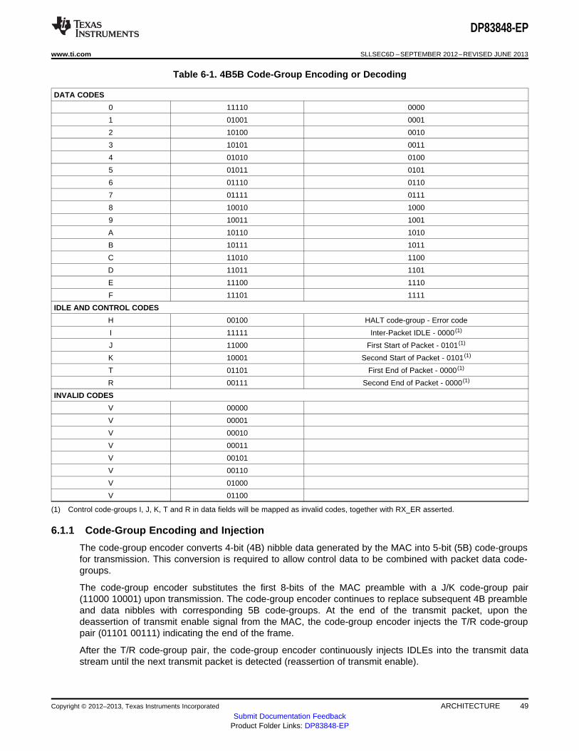
DP83848-EP
www.ti.com SLLSEC6D –SEPTEMBER 2012–REVISED JUNE 2013
Table 6-1. 4B5B Code-Group Encoding or Decoding
DATA CODES
0 11110 0000
1 01001 0001
2 10100 0010
3 10101 0011
4 01010 0100
5 01011 0101
6 01110 0110
7 01111 0111
8 10010 1000
9 10011 1001
A 10110 1010
B 10111 1011
C 11010 1100
D 11011 1101
E 11100 1110
F 11101 1111
IDLE AND CONTROL CODES
H 00100 HALT code-group - Error code
I 11111 Inter-Packet IDLE - 0000 (1)
J 11000 First Start of Packet - 0101 (1)
K 10001 Second Start of Packet - 0101 (1)
T 01101 First End of Packet - 0000 (1)
R 00111 Second End of Packet - 0000 (1)
INVALID CODES
V 00000
V 00001
V 00010
V 00011
V 00101
V 00110
V 01000
V 01100
(1) Control code-groups I, J, K, T and R in data fields will be mapped as invalid codes, together with RX_ER asserted.
6.1.1 Code-Group Encoding and Injection
The code-group encoder converts 4-bit (4B) nibble data generated by the MAC into 5-bit (5B) code-groupsfor transmission. This conversion is required to allow control data to be combined with packet data code-groups.
The code-group encoder substitutes the first 8-bits of the MAC preamble with a J/K code-group pair(11000 10001) upon transmission. The code-group encoder continues to replace subsequent 4B preambleand data nibbles with corresponding 5B code-groups. At the end of the transmit packet, upon thedeassertion of transmit enable signal from the MAC, the code-group encoder injects the T/R code-grouppair (01101 00111) indicating the end of the frame.
After the T/R code-group pair, the code-group encoder continuously injects IDLEs into the transmit datastream until the next transmit packet is detected (reassertion of transmit enable).
Copyright © 2012–2013, Texas Instruments Incorporated ARCHITECTURE 49Submit Documentation Feedback
Product Folder Links: DP83848-EP

DP83848-EP
SLLSEC6D –SEPTEMBER 2012–REVISED JUNE 2013 www.ti.com
6.1.2 Scrambler
The scrambler is required to control the radiated emissions at the media connector and on the twisted paircable (for 100BASE-TX applications). By scrambling the data, the total energy launched onto the cable israndomly distributed over a wide frequency range. Without the scrambler, energy levels at the PMD andon the cable could peak beyond FCC limitations at frequencies related to repeating 5B sequences (i.e.,continuous transmission of IDLEs).
The scrambler is configured as a closed loop linear feedback shift register (LFSR) with an 11-bitpolynomial. The output of the closed loop LFSR is X-ORd with the serial NRZ data from the code-groupencoder. The result is a scrambled data stream with sufficient randomization to decrease radiatedemissions at certain frequencies by as much as 20 dB. The DP83848 uses the PHY_ID (pins PHYAD[4:0]) to set a unique seed value.
6.1.3 NRZ to NRZI Encoder
After the transmit data stream has been serialized and scrambled, the data must be NRZI encoded inorder to comply with the TP-PMD standard for 100BASE-TX transmission over Category-5 Unshieldedtwisted pair cable.
6.1.4 Binary to MLT-3 Convertor
The binary to MLT-3 conversion is accomplished by converting the serial binary data stream output fromthe NRZI encoder into two binary data streams with alternately phased logic one events. These two binarystreams are then fed to the twisted pair output driver which converts the voltage to current and alternatelydrives either side of the transmit transformer primary winding, resulting in a MLT-3 signal.
The 100BASE-TX MLT-3 signal sourced by the PMD output pair common driver is slew rate controlled.This should be considered when selecting AC coupling magnetics to ensure TP-PMD standard complianttransition times (3 ns < Tr < 5 ns).
The 100BASE-TX transmit TP-PMD function within the DP83848 is capable of sourcing only MLT-3encoded data. Binary output from the PMD output pair is not possible in 100 Mb/s mode.
6.2 100BASE-TX Receiver
The 100BASE-TX receiver consists of several functional blocks which convert the scrambled MLT-3 125Mb/s serial data stream to synchronous 4-bit nibble data that is provided to the MII. Because the100BASE-TX TP-PMD is integrated, the differential input pins, RD±, can be directly routed from the ACcoupling magnetics.
See Figure 6-2 for a block diagram of the 100BASE-TX receive function. This provides an overview ofeach functional block within the 100BASE-TX receive section.
The receive section consists of the following functional blocks:• Analog front end• Digital signal processor• Signal detect• MLT-3 to binary decoder• NRZI to NRZ decoder• Serial to parallel• Descrambler• Code group alignment• 4B/5B decoder• Link integrity monitor• Bad SSD detection
50 ARCHITECTURE Copyright © 2012–2013, Texas Instruments Incorporated
Submit Documentation FeedbackProduct Folder Links: DP83848-EP

4B/5B Decoder
RX_CLK RXD[3:0] / RX_ERRX_DV/CRS
Serial to Parallel
Code GroupAlignment
Descrambler
NRZI-to-NRZDecoder
MLT-3 to BinaryDecoder
RX_DATAValid SSD
Detect
DigitalSignal
Processor
AnalogFrontEnd
LinkIntegrityMonitor
Signal Detect
RD ±
DP83848-EP
www.ti.com SLLSEC6D –SEPTEMBER 2012–REVISED JUNE 2013
6.2.1 Analog Front End
In addition to the digital equalization and gain control, the DP83848 includes analog equalization and gaincontrol in the analog front end. The analog equalization reduces the amount of digital equalizationrequired in the DSP.
6.2.2 Digital Signal Processor
The digital signal processor includes adaptive equalization with gain control and base line wandercompensation.
Figure 6-2. 100BASE-TX Receive Block Diagram
Copyright © 2012–2013, Texas Instruments Incorporated ARCHITECTURE 51Submit Documentation Feedback
Product Folder Links: DP83848-EP

Attenuation versus Frequency
Frequency (MHz)
Attenuation (
dB
)
30
25
20
15
10
5
00 20 40 60 80 100 120
35
150m
130m
100m
50m
0m
DP83848-EP
SLLSEC6D –SEPTEMBER 2012–REVISED JUNE 2013 www.ti.com
6.2.2.1 Digital Adaptive Equalization and Gain Control
When transmitting data at high speeds over copper twisted pair cable, frequency dependent attenuationbecomes a concern. In high-speed twisted pair signalling, the frequency content of the transmitted signalcan vary greatly during normal operation based primarily on the randomness of the scrambled datastream. This variation in signal attenuation caused by frequency variations must be compensated toensure the integrity of the transmission.
In order to ensure quality transmission when employing MLT-3 encoding, the compensation must be ableto adapt to various cable lengths and cable types depending on the installed environment. The selection oflong cable lengths for a given implementation, requires significant compensation which will over-compensate for shorter, less attenuating lengths. Conversely, the selection of short or intermediate cablelengths requiring less compensation will cause serious under-compensation for longer length cables. Thecompensation or equalization must be adaptive to ensure proper conditioning of the received signalindependent of the cable length.
The DP83848 utilizes an extremely robust equalization scheme referred as ‘digital adaptive equalization’.
The digital equalizer removes inter symbol interference (ISI) from the receive data stream by continuouslyadapting to provide a filter with the inverse frequency response of the channel. Equalization is combinedwith an adaptive gain control stage. This enables the receive 'eye pattern' to be opened sufficiently toallow very reliable data recovery.
The curves given in Figure 6-3 illustrate attenuation at certain frequencies for given cable lengths. This isderived from the worst case frequency vs. attenuation figures as specified in the EIA/TIA Bulletin TSB-36.These curves indicate the significant variations in signal attenuation that must be compensated for by thereceive adaptive equalization circuit.
Figure 6-3. EIA/TIA Attenuation vs. Frequency for 0, 50, 100, 130 and 150 meters of CAT 5 cable
52 ARCHITECTURE Copyright © 2012–2013, Texas Instruments Incorporated
Submit Documentation FeedbackProduct Folder Links: DP83848-EP

DP83848-EP
www.ti.com SLLSEC6D –SEPTEMBER 2012–REVISED JUNE 2013
6.2.2.2 Base Line Wander Compensation
Figure 6-4. 100BASE-TX BLW Event
The DP83848 is completely ANSI TP-PMD compliant and includes base line wander (BLW)compensation. The BLW compensation block can successfully recover the TPPMD defined “killer” pattern.
BLW can generally be defined as the change in the average DC content, relatively short period over time,of an AC coupled digital transmission over a given transmission medium. (i.e., copper wire).
BLW results from the interaction between the low frequency components of a transmitted bit stream andthe frequency response of the AC coupling components within the transmission system. If the lowfrequency content of the digital bit stream goes below the low frequency pole of the AC couplingtransformers then the droop characteristics of the transformers will dominate resulting in potentiallyserious BLW.
The digital oscilloscope plot provided in Figure 6-4 illustrates the severity of the BLW event that cantheoretically be generated during 100BASE-TX packet transmission. This event consists of approximately800 mV of DC offset for a period of 120 μs. Left uncompensated, events such as this can cause packetloss.
6.2.3 Signal Detect
The signal detect function of the DP83848 is incorporated to meet the specifications mandated by theANSI FDDI TP-PMD Standard as well as the IEEE 802.3 100BASE-TX Standard for both voltagethresholds and timing parameters.
Note that the reception of normal 10BASE-T link pulses and fast link pulses per IEEE 802.3u auto-negotiation by the 100BASE-TX receiver do not cause the DP83848 to assert signal detect.
6.2.4 MLT-3 to NRZI Decoder
The DP83848 decodes the MLT-3 information from the Digital Adaptive Equalizer block to binary NRZIdata.
6.2.5 NRZI to NRZ
In a typical application, the NRZI to NRZ decoder is required in order to present NRZ formatted data to thedescrambler.
Copyright © 2012–2013, Texas Instruments Incorporated ARCHITECTURE 53Submit Documentation Feedback
Product Folder Links: DP83848-EP

DP83848-EP
SLLSEC6D –SEPTEMBER 2012–REVISED JUNE 2013 www.ti.com
6.2.6 Serial to Parallel
The 100BASE-TX receiver includes a serial to parallel converter which supplies 5-bit wide data symbols tothe PCS Rx state machine.
6.2.7 Descrambler
A serial descrambler is used to de-scramble the received NRZ data. The descrambler has to generate anidentical data scrambling sequence (N) in order to recover the original unscrambled data (UD) from thescrambled data (SD) as represented in the equations:SD = (UD ⊕ N) (1)UD = (SD ⊕ N) (2)
Synchronization of the descrambler to the original scrambling sequence (N) is achieved based on theknowledge that the incoming scrambled data stream consists of scrambled IDLE data. After thedescrambler has recognized 12 consecutive IDLE code-groups, where an unscrambled IDLE code-groupin 5B NRZ is equal to five consecutive ones (11111), it will synchronize to the receive data stream andgenerate unscrambled data in the form of unaligned 5B code-groups.
In order to maintain synchronization, the descrambler must continuously monitor the validity of theunscrambled data that it generates. To ensure this, a line state monitor and a hold timer are used toconstantly monitor the synchronization status. Upon synchronization of the descrambler the hold timerstarts a 722 μs countdown. Upon detection of sufficient IDLE code-groups (58 bit times) within the 722 μsperiod, the hold timer will reset and begin a new countdown. This monitoring operation will continueindefinitely given a properly operating network connection with good signal integrity. If the line statemonitor does not recognize sufficient unscrambled IDLE code-groups within the 722 μs period, the entiredescrambler will be forced out of the current state of synchronization and reset in order to reacquiresynchronization.
6.2.8 Code-Group Alignment
The code-group alignment module operates on unaligned 5-bit data from the descrambler (or, if thedescrambler is bypassed, directly from the NRZI/NRZ decoder) and converts it into 5B code-group data (5bits). Code-group alignment occurs after the J/K code-group pair is detected. Once the J/K code-grouppair (11000 10001) is detected, subsequent data is aligned on a fixed boundary.
6.2.9 4B/5B Decoder
The code-group decoder functions as a look up table that translates incoming 5B code-groups into 4Bnibbles. The code-group decoder first detects the J/K code-group pair preceded by IDLE code-groups andreplaces the J/K with MAC preamble. Specifically, the J/K 10-bit code-group pair is replaced by the nibblepair (0101 0101). All subsequent 5B code-groups are converted to the corresponding 4B nibbles for theduration of the entire packet. This conversion ceases upon the detection of the T/R code-group pairdenoting the end of stream delimiter (ESD) or with the reception of a minimum of two IDLE code-groups.
6.2.10 100BASE-TX Link Integrity Monitor
The 100 Base TX Link monitor ensures that a valid and stable link is established before enabling both thetransmit and receive PCS layer.
Signal detect must be valid for 395 µs to allow the link monitor to enter the link up state, and enable thetransmit and receive functions.
54 ARCHITECTURE Copyright © 2012–2013, Texas Instruments Incorporated
Submit Documentation FeedbackProduct Folder Links: DP83848-EP
DP83848-EP
www.ti.com SLLSEC6D –SEPTEMBER 2012–REVISED JUNE 2013
6.2.11 Bad SSD Detection
A bad start of stream delimiter (Bad SSD) is any transition from consecutive idle code-groups to non-idlecode-groups which is not prefixed by the code-group pair /J/K.
If this condition is detected, the DP83848 will assert RX_ER and present RXD[3:0] = 1110 to the MII forthe cycles that correspond to received 5B code-groups until at least two IDLE code groups are detected.In addition, the false carrier sense counter register (FCSCR) will be incremented by one.
Once at least two IDLE code groups are detected, RX_ER and CRS become de-asserted.
6.3 10BASE-T Transceiver Module
The 10BASE-T transceiver module is IEEE 802.3 compliant. It includes the receiver, transmitter, collision,heartbeat, loopback, jabber, and link integrity functions, as defined in the standard. An external filter is notrequired on the 10BASE-T interface since this is integrated inside the DP83848. This section focuses onthe general 10BASET system level operation.
6.3.1 Operational Modes
6.3.1.1 Half Duplex Mode
In half duplex mode the DP83848 functions as a standard IEEE 802.3 10BASE-T transceiver supportingthe CSMA/CD protocol.
6.3.1.2 Full Duplex Mode
In full duplex mode the DP83848 is capable of simultaneously transmitting and receiving without assertingthe collision signal. The DP83848's 10 Mb/s ENDEC is designed to encode and decode simultaneously.
6.3.2 Smart Squelch
The smart squelch is responsible for determining when valid data is present on the differential receiveinputs. The DP83848 implements an intelligent receive squelch to ensure that impulse noise on thereceive inputs will not be mistaken for a valid signal. Smart squelch operation is independent of the10BASE-T operational mode.
The squelch circuitry employs a combination of amplitude and timing measurements (as specified in theIEEE 802.3 10BSE-T standard) to determine the validity of data on the twisted pair inputs (refer toFigure 6-5).
The signal at the start of a packet is checked by the smart squelch and any pulses not exceeding thesquelch level (either positive or negative, depending upon polarity) will be rejected. Once this first squelchlevel is overcome correctly, the opposite squelch level must then be exceeded within 150 ns. Finally thesignal must again exceed the original squelch level within a 150 ns to ensure that the input waveform willnot be rejected. This checking procedure results in the loss of typically three preamble bits at thebeginning of each packet.
Only after all these conditions have been satisfied will a control signal be generated to indicate to theremainder of the circuitry that valid data is present. At this time, the smart squelch circuitry is reset.
Valid data is considered to be present until the squelch level has not been generated for a time longerthan 150 ns, indicating the end of packet. Once good data has been detected, the squelch levels arereduced to minimize the effect of noise causing premature end of packet detection.
Copyright © 2012–2013, Texas Instruments Incorporated ARCHITECTURE 55Submit Documentation Feedback
Product Folder Links: DP83848-EP

<150 ns <150 ns >150 ns
Start of packet End of packet
VSQ+
VSQ+(reduced)
VSQ–(reduced)
VSQ–
DP83848-EP
SLLSEC6D –SEPTEMBER 2012–REVISED JUNE 2013 www.ti.com
Figure 6-5. 10BASE-T Twisted Pair Smart Squelch Operation
6.3.3 Collision Detection and SQE
When in half duplex, a 10BASE-T collision is detected when the receive and transmit channels are activesimultaneously. Collisions are reported by the COL signal on the MII. Collisions are also reported when ajabber condition is detected.
The COL signal remains set for the duration of the collision. If the PHY is receiving when a collision isdetected it is reported immediately (through the COL pin).
When heartbeat is enabled, approximately 1 μs after the transmission of each packet, a signal qualityerror (SQE) signal of approximately 10-bit times is generated to indicate successful transmission. SQE isreported as a pulse on the COL signal of the MII.
The SQE test is inhibited when the PHY is set in full duplex mode. SQE can also be inhibited by settingthe HEARTBEAT_DIS bit in the 10BTSCR register.
6.3.4 Carrier Sense
Carrier sense (CRS) may be asserted due to receive activity once valid data is detected via the squelchfunction.
For 10 Mb/s half Dduplex operation, CRS is asserted during either packet transmission or reception.
For 10 Mb/s full duplex operation, CRS is asserted only during receive activity.
CRS is deasserted following an end of packet.
6.3.5 Normal Link Pulse Detection/Generation
The link pulse generator produces pulses as defined in the IEEE 802.3 10BASE-T standard. Each linkpulse is nominally 100 ns in duration and transmitted every 16 ms in the absence of transmit data.
Link pulses are used to check the integrity of the connection with the remote end. If valid link pulses arenot received, the link detector disables the 10BASE-T twisted pair transmitter, receiver and collisiondetection functions.
When the link integrity function is disabled (FORCE_LINK_10 of the 10BTSCR register), a good link isforced and the 10BASE-T transceiver will operate regardless of the presence of link pulses.
6.3.6 Jabber Function
The jabber function monitors the DP83848's output and disables the transmitter if it attempts to transmit apacket of longer than legal size. A jabber timer monitors the transmitter and disables the transmission ifthe transmitter is active for approximately 85 ms.
56 ARCHITECTURE Copyright © 2012–2013, Texas Instruments Incorporated
Submit Documentation FeedbackProduct Folder Links: DP83848-EP

DP83848-EP
www.ti.com SLLSEC6D –SEPTEMBER 2012–REVISED JUNE 2013
Once disabled by the Jabber function, the transmitter stays disabled for the entire time that the ENDECmodule's internal transmit enable is asserted. This signal has to be deasserted for approximately 500 ms(the “unjab” time) before the Jabber function re-enables the transmit outputs.
The Jabber function is only relevant in 10BASE-T mode.
6.3.7 Automatic Link Polarity Detection and Correction
The DP83848's 10BASE-T transceiver module incorporates an automatic link polarity detection circuit.When three consecutive inverted link pulses are received, bad polarity is reported.
A polarity reversal can be caused by a wiring error at either end of the cable, usually at the maindistribution frame (MDF) or patch panel in the wiring closet.
The bad polarity condition is latched in the 10BTSCR register. The DP83848's 10BASE-T transceivermodule corrects for this error internally and will continue to decode received data correctly. This eliminatesthe need to correct the wiring error immediately.
6.3.8 Transmit and Receive Filtering
External 10BASE-T filters are not required when using the DP83848, as the required signal conditioning isintegrated into the device.
Only isolation transformers and impedance matching resistors are required for the 10BASE-T transmit andreceive interface. The internal transmit filtering ensures that all the harmonics in the transmit signal areattenuated by at least 30 dB.
6.3.9 Transmitter
The encoder begins operation when the transmit enable input (TX_EN) goes high and converts NRZ datato preemphasized Manchester data for the transceiver. For the duration of TX_EN, the serialized transmitdata (TXD) is encoded for the transmit-driver pair (PMD Output Pair). TXD must be valid on the risingedge of transmit clock (TX_CLK). Transmission ends when TX_EN deasserts. The last transition is alwayspositive; it occurs at the center of the bit cell if the last bit is a one, or at the end of the bit cell if the last bitis a zero.
6.3.10 Receiver
The decoder detects the end of a frame when no additional mid-bit transitions are detected. Within oneand a half bit times after the last bit, carrier sense is de-asserted. Receive clock stays active for five morebit times after CRS goes low, to guarantee the receive timings of the controller.
Copyright © 2012–2013, Texas Instruments Incorporated ARCHITECTURE 57Submit Documentation Feedback
Product Folder Links: DP83848-EP
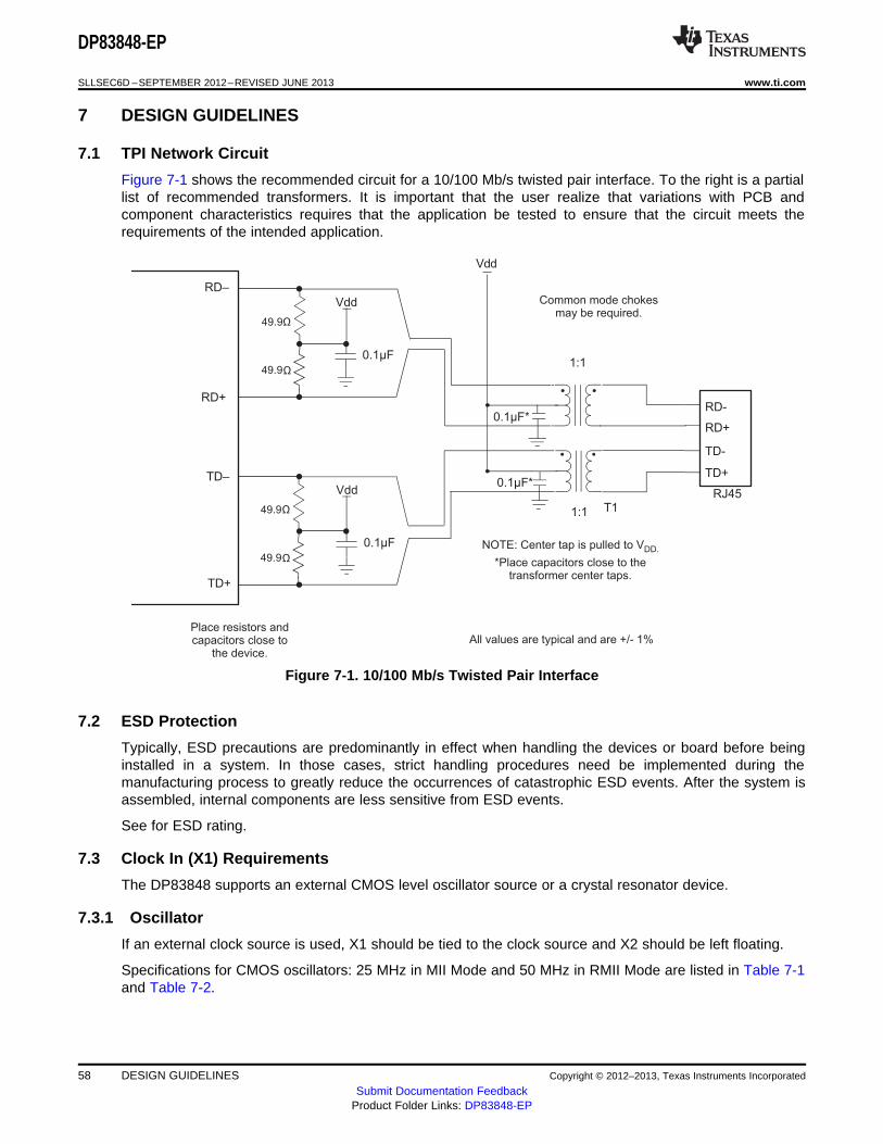
RJ45
RD–
RD+
TD–
TD+
RD-
RD+
TD-
TD+
1:1
0.1μF*
T1
1:1
49.9Ω
49.9Ω
0.1μF*
Vdd
NOTE: Center tap is pulled to VDD.
0.1µF
All values are typical and are +/- 1%
Vdd
49.9Ω
49.9Ω
0.1µF
Vdd
*Place capacitors close to thetransformer center taps.
Place resistors andcapacitors close to
the device.
Common mode chokesmay be required.
DP83848-EP
SLLSEC6D –SEPTEMBER 2012–REVISED JUNE 2013 www.ti.com
7 DESIGN GUIDELINES
7.1 TPI Network Circuit
Figure 7-1 shows the recommended circuit for a 10/100 Mb/s twisted pair interface. To the right is a partiallist of recommended transformers. It is important that the user realize that variations with PCB andcomponent characteristics requires that the application be tested to ensure that the circuit meets therequirements of the intended application.
Figure 7-1. 10/100 Mb/s Twisted Pair Interface
7.2 ESD Protection
Typically, ESD precautions are predominantly in effect when handling the devices or board before beinginstalled in a system. In those cases, strict handling procedures need be implemented during themanufacturing process to greatly reduce the occurrences of catastrophic ESD events. After the system isassembled, internal components are less sensitive from ESD events.
See for ESD rating.
7.3 Clock In (X1) Requirements
The DP83848 supports an external CMOS level oscillator source or a crystal resonator device.
7.3.1 Oscillator
If an external clock source is used, X1 should be tied to the clock source and X2 should be left floating.
Specifications for CMOS oscillators: 25 MHz in MII Mode and 50 MHz in RMII Mode are listed in Table 7-1and Table 7-2.
58 DESIGN GUIDELINES Copyright © 2012–2013, Texas Instruments Incorporated
Submit Documentation FeedbackProduct Folder Links: DP83848-EP
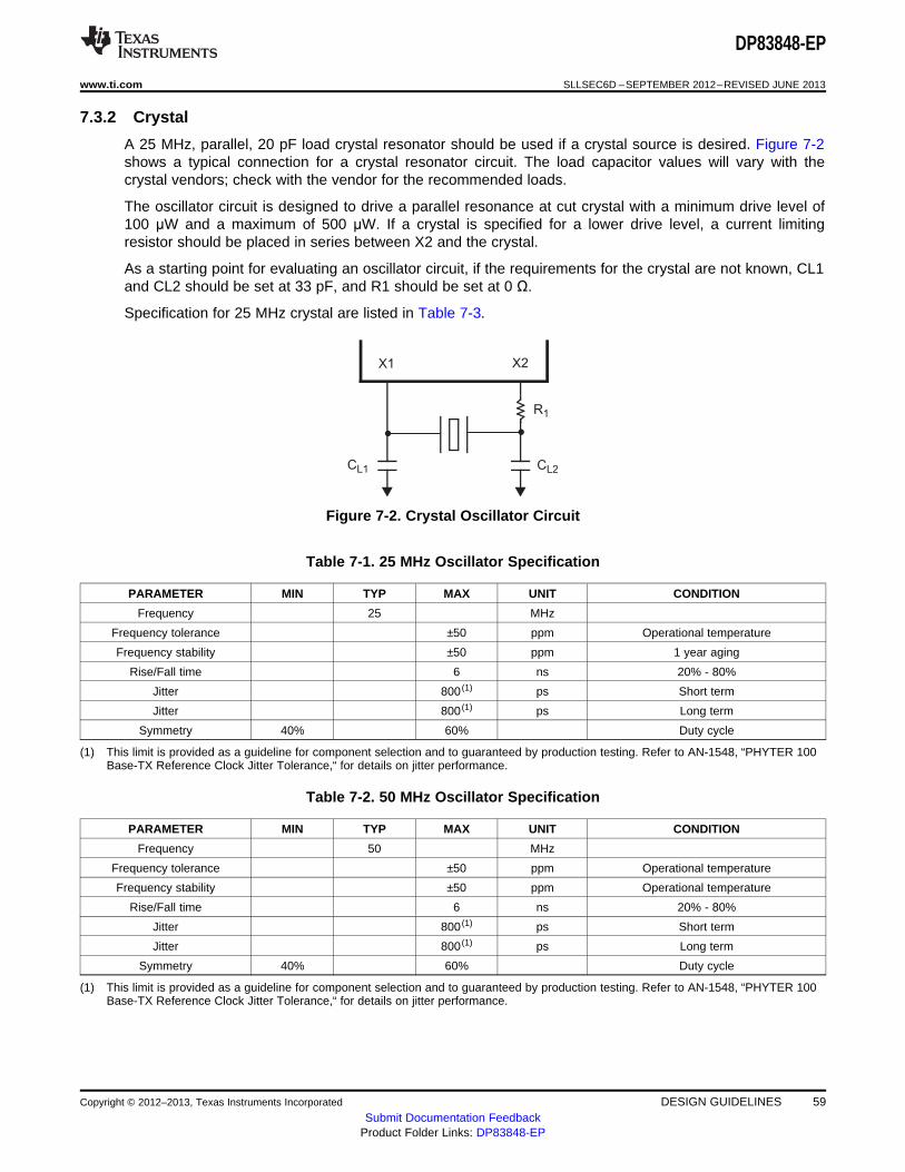
X1 X2
CL2CL1
R1
DP83848-EP
www.ti.com SLLSEC6D –SEPTEMBER 2012–REVISED JUNE 2013
7.3.2 Crystal
A 25 MHz, parallel, 20 pF load crystal resonator should be used if a crystal source is desired. Figure 7-2shows a typical connection for a crystal resonator circuit. The load capacitor values will vary with thecrystal vendors; check with the vendor for the recommended loads.
The oscillator circuit is designed to drive a parallel resonance at cut crystal with a minimum drive level of100 μW and a maximum of 500 μW. If a crystal is specified for a lower drive level, a current limitingresistor should be placed in series between X2 and the crystal.
As a starting point for evaluating an oscillator circuit, if the requirements for the crystal are not known, CL1and CL2 should be set at 33 pF, and R1 should be set at 0 Ω.
Specification for 25 MHz crystal are listed in Table 7-3.
Figure 7-2. Crystal Oscillator Circuit
Table 7-1. 25 MHz Oscillator Specification
PARAMETER MIN TYP MAX UNIT CONDITION
Frequency 25 MHz
Frequency tolerance ±50 ppm Operational temperature
Frequency stability ±50 ppm 1 year aging
Rise/Fall time 6 ns 20% - 80%
Jitter 800 (1) ps Short term
Jitter 800 (1) ps Long term
Symmetry 40% 60% Duty cycle
(1) This limit is provided as a guideline for component selection and to guaranteed by production testing. Refer to AN-1548, “PHYTER 100Base-TX Reference Clock Jitter Tolerance,“ for details on jitter performance.
Table 7-2. 50 MHz Oscillator Specification
PARAMETER MIN TYP MAX UNIT CONDITION
Frequency 50 MHz
Frequency tolerance ±50 ppm Operational temperature
Frequency stability ±50 ppm Operational temperature
Rise/Fall time 6 ns 20% - 80%
Jitter 800 (1) ps Short term
Jitter 800 (1) ps Long term
Symmetry 40% 60% Duty cycle
(1) This limit is provided as a guideline for component selection and to guaranteed by production testing. Refer to AN-1548, “PHYTER 100Base-TX Reference Clock Jitter Tolerance,“ for details on jitter performance.
Copyright © 2012–2013, Texas Instruments Incorporated DESIGN GUIDELINES 59Submit Documentation Feedback
Product Folder Links: DP83848-EP
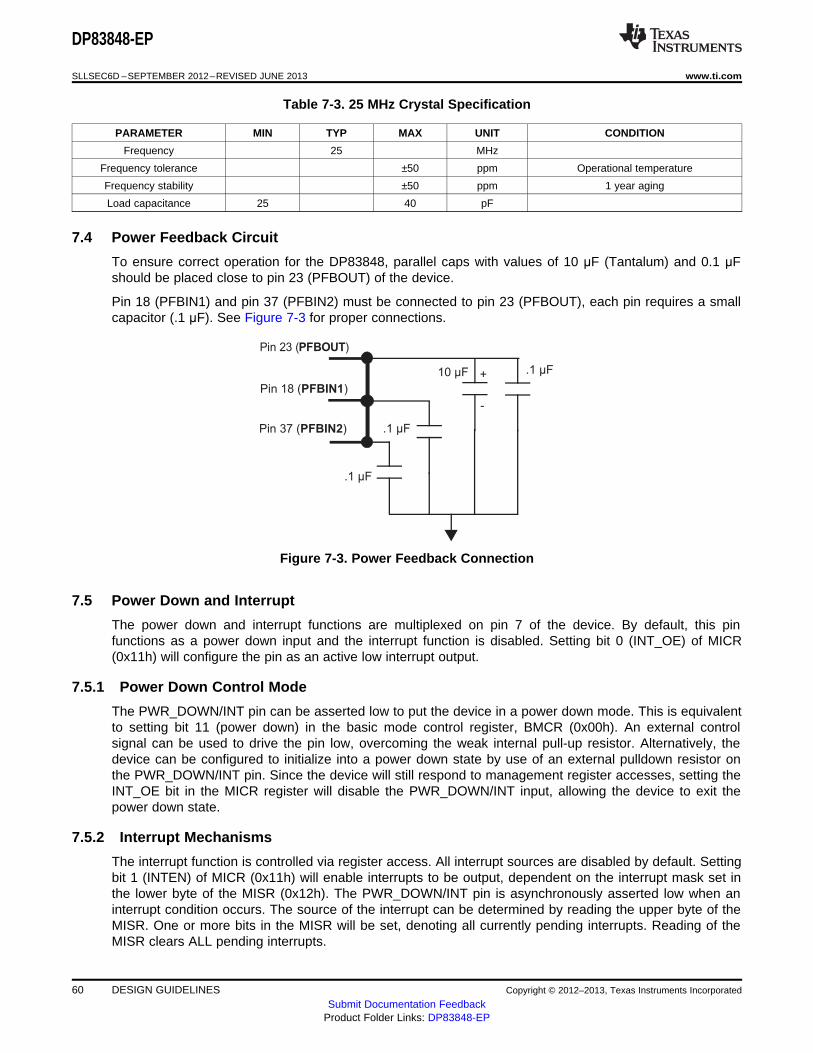
.1 µF10 µF
Pin 23 (PFBOUT)
.1 µF
.1 µF
Pin 18 (PFBIN1)
Pin 37 (PFBIN2)
+
-
DP83848-EP
SLLSEC6D –SEPTEMBER 2012–REVISED JUNE 2013 www.ti.com
Table 7-3. 25 MHz Crystal Specification
PARAMETER MIN TYP MAX UNIT CONDITION
Frequency 25 MHz
Frequency tolerance ±50 ppm Operational temperature
Frequency stability ±50 ppm 1 year aging
Load capacitance 25 40 pF
7.4 Power Feedback Circuit
To ensure correct operation for the DP83848, parallel caps with values of 10 μF (Tantalum) and 0.1 μFshould be placed close to pin 23 (PFBOUT) of the device.
Pin 18 (PFBIN1) and pin 37 (PFBIN2) must be connected to pin 23 (PFBOUT), each pin requires a smallcapacitor (.1 μF). See Figure 7-3 for proper connections.
Figure 7-3. Power Feedback Connection
7.5 Power Down and Interrupt
The power down and interrupt functions are multiplexed on pin 7 of the device. By default, this pinfunctions as a power down input and the interrupt function is disabled. Setting bit 0 (INT_OE) of MICR(0x11h) will configure the pin as an active low interrupt output.
7.5.1 Power Down Control Mode
The PWR_DOWN/INT pin can be asserted low to put the device in a power down mode. This is equivalentto setting bit 11 (power down) in the basic mode control register, BMCR (0x00h). An external controlsignal can be used to drive the pin low, overcoming the weak internal pull-up resistor. Alternatively, thedevice can be configured to initialize into a power down state by use of an external pulldown resistor onthe PWR_DOWN/INT pin. Since the device will still respond to management register accesses, setting theINT_OE bit in the MICR register will disable the PWR_DOWN/INT input, allowing the device to exit thepower down state.
7.5.2 Interrupt Mechanisms
The interrupt function is controlled via register access. All interrupt sources are disabled by default. Settingbit 1 (INTEN) of MICR (0x11h) will enable interrupts to be output, dependent on the interrupt mask set inthe lower byte of the MISR (0x12h). The PWR_DOWN/INT pin is asynchronously asserted low when aninterrupt condition occurs. The source of the interrupt can be determined by reading the upper byte of theMISR. One or more bits in the MISR will be set, denoting all currently pending interrupts. Reading of theMISR clears ALL pending interrupts.
60 DESIGN GUIDELINES Copyright © 2012–2013, Texas Instruments Incorporated
Submit Documentation FeedbackProduct Folder Links: DP83848-EP

DP83848-EP
www.ti.com SLLSEC6D –SEPTEMBER 2012–REVISED JUNE 2013
Example: To generate an interrupt on a change of link status or on a change of energy detect power state,the steps would be:• Write 0003h to MICR to set INTEN and INT_OE• Write 0060h to MISR to set ED_INT_EN and LINK_INT_EN• Monitor PWR_DOWN/INT pin
When PWR_DOWN/INT pin asserts low, user would read the MISR register to see if the ED_INT orLINK_INT bits are set, i.e. which source caused the interrupt. After reading the MISR, the interrupt bitsshould clear and the PWR_DOWN/INT pin will deassert.
7.6 Energy Detect Mode
When energy detect is enabled and there is no activity on the cable, the DP83848 will remain in a lowpower mode while monitoring the transmission line. Activity on the line will cause the DP83848 to gothrough a normal power up sequence. Regardless of cable activity, the DP83848 will occasionally wakeup the transmitter to put ED pulses on the line, but will otherwise draw as little power as possible. Energydetect functionality is controlled via register energy detect control (EDCR), address 0x1Dh.
7.7 Thermal Vias Recommendation
The following thermal via guidelines apply to GNDPAD, pin 49:
1. Thermal via size = 0.2 mm
2. Recommend 4 vias
3. Vias have a center to center separation of 2 mm
Adherence to this guideline is required to achieve the intended operating temperature range of the device.
Figure 7-4 illustrates an example layout.
Figure 7-4. Top View, Thermal Vias for GNDPAD, Pin 49
Copyright © 2012–2013, Texas Instruments Incorporated DESIGN GUIDELINES 61Submit Documentation Feedback
Product Folder Links: DP83848-EP

DP83848-EP
SLLSEC6D –SEPTEMBER 2012–REVISED JUNE 2013 www.ti.com
62 DESIGN GUIDELINES Copyright © 2012–2013, Texas Instruments Incorporated
Submit Documentation FeedbackProduct Folder Links: DP83848-EP

DP83848-EP
www.ti.com SLLSEC6D –SEPTEMBER 2012–REVISED JUNE 2013
8 RESET OPERATION
The DP83848 includes an internal power-on reset (POR) function and does not need to be explicitly resetfor normal operation after power up. If required during normal operation, the device can be reset by ahardware or software reset.
8.1 Hardware Reset
A hardware reset is accomplished by applying a low pulse (TTL level), with a duration of at least 1 μs, tothe RESET_N. This will reset the device such that all registers will be reinitialized to default values and thehardware configuration values will be re-latched into the device (similar to the power-up/reset operation).
8.2 Software Reset
A software reset is accomplished by setting the reset bit (bit 15) of the basic mode control register(BMCR). The period from the point in time when the reset bit is set to the point in time when softwarereset has concluded is approximately 1 μs.
The software reset will reset the device such that all registers will be reset to default values and thehardware configuration values will be maintained. Software driver code must wait 3 μs following a softwarereset before allowing further serial MII operations with the DP83848.
Copyright © 2012–2013, Texas Instruments Incorporated RESET OPERATION 63Submit Documentation Feedback
Product Folder Links: DP83848-EP

DP83848-EP
SLLSEC6D –SEPTEMBER 2012–REVISED JUNE 2013 www.ti.com
9 REGISTER BLOCK
9.1 Table 9-1. Register Map
OFFSETACCESS TAG DESCRIPTION
HEX DECIMAL
00h 0 RW BMCR Basic Mode Control Register
01h 1 RO BMSR Basic Mode Status Register
02h 2 RO PHYIDR1 PHY Identifier Register #1
03h 3 RO PHYIDR2 PHY Identifier Register #2
04h 4 RW ANAR Auto-Negotiation Advertisement Register
Auto-Negotiation Link Partner Ability Register (Base05h 5 RW ANLPAR Page)
Auto-Negotiation Link Partner Ability Register (Next05h 5 RW ANLPARNP Page)
06h 6 RW ANER Auto-Negotiation Expansion Register
07h 7 RW ANNPTR Auto-Negotiation Next Page TX
08h-Fh 15-Aug RW RESERVED RESERVED
EXTENDED REGISTERS
10h 16 RO PHYSTS PHY Status Register
11h 17 RW MICR MII Interrupt Control Register
12h 18 RO MISR MII Interrupt Status Register
13h 19 RW RESERVED RESERVED
14h 20 RO FCSCR False Carrier Sense Counter Register
15h 21 RO RECR Receive Error Counter Register
16h 22 RW PCSR PCS Sub-Layer Configuration and Status Register
17h 23 RW RBR RMII and Bypass Register
18h 24 RW LEDCR LED Direct Control Register
19h 25 RW PHYCR PHY Control Register
1Ah 26 RW 10BTSCR 10Base-T Status/Control Register
CD Test Control Register and BIST Extensions1Bh 27 RW CDCTRL1 Register
1Ch 28 RW RESERVED RESERVED
1Dh 29 RW EDCR Energy Detect Control Register
1Eh-1Fh 30-31 RW RESERVED RESERVED
64 REGISTER BLOCK Copyright © 2012–2013, Texas Instruments Incorporated
Submit Documentation FeedbackProduct Folder Links: DP83848-EP

DP83848-EP
www.ti.com SLLSEC6D –SEPTEMBER 2012–REVISED JUNE 2013
Table 9-2. Register Table
REGISTER ADDRESS TAG BIT 15 BIT 14 BIT 13 BIT 12 BIT 11 BIT 10 BIT 9 BIT 8 BIT 7 BIT 6 BIT 5 BIT 4 BIT 3 BIT 2 BIT 1 BIT0NAME
Basic Mode Auto- RestartLoop- Speed Power Duplex Collision Re- Re- Re- Re- Re- Re- Re-Control 00h BMCR Reset Neg Isolate Auto-back Selection Down Mode Test served served served served served served servedRegister Enable Neg
MF Pre- Auto- Extend-Basic Mode Auto-100Base 100Base 100Base 10Base- 10Base- Re- Re- Re- Re- amble Neg Remote Link Jabber edStatus 01h BMSR Neg-T4 -TX FDX -TX HDX T FDX T HDX served served served served Sup- Com- Fault Status Detect Capa-Register Abilitypress plete bility
PHY PHYIDR OUI OUI OUI OUI OUI OUI OUI OUI OUI OUI OUI OUI OUI OUI OUI OUIIdentifier 02h 1 MSB MSB MSB MSB MSB MSB MSB MSB MSB MSB MSB MSB MSB MSB MSB MSBRegister 1
PHY PHYIDR VNDR_ VNDR_ VNDR_ VNDR_ VNDR_ VNDR_ MDL_ MDL_ MDL_ MDL_Identifier 03h OUI LSB OUI LSB OUI LSB OUI LSB OUI LSB OUI LSB2 MDL MDL MDL MDL MDL MDL REV REV REV REVRegister 2
Auto-Negotiation Next Re- Remote Re- ASM_ Protocol Protocol Protocol Protocol ProtocolAdvertise- 04h ANAR PAUSE T4 TX_FD TX 10_FD 10Page Ind served Fault served DIR Selection Selection Selection Selection Selectionment
Register
Auto-NegotiationLink Partner Next Remote Re- ASM_ Protocol Protocol Protocol Protocol Protocol05h ANLPAR ACK PAUSE T4 TX_FD TX 10_FD 10Ability Page Ind Fault served DIR Selection Selection Selection Selection Selection
Register(Base Page)
Auto-Negotiation Mes-Link Partner AN- Next05h ACK sage ACK2 Toggle Code Code Code Code Code Code Code Code Code Code CodeAbility LPARNP Page Ind PageRegister Next
Page
Auto-Negotiation Re- Re- Re- Re- Re- Re- Re- Re- Re- Re- Re- LP_NP_ NP_ PAGE_ LP_AN_06h ANER PDFExpansion served served served served served served served served served served served ABLE ABLE RX ABLE
Register
Auto-Negotiation Next Re- Message07h ANNPTR ACK2 TOG_TX CODE CODE CODE CODE CODE CODE CODE CODE CODE CODE CODENext Page Page Ind served PageTX Register
Re- Re- Re- Re- Re- Re- Re- Re- Re- Re- Re- Re- Re- Re- Re- Re- Re-Reserved 08-0fh served served served served served served served served served served served served served served served served served
Copyright © 2012–2013, Texas Instruments Incorporated REGISTER BLOCK 65Submit Documentation Feedback
Product Folder Links: DP83848-EP

DP83848-EP
SLLSEC6D –SEPTEMBER 2012–REVISED JUNE 2013 www.ti.com
Table 9-2. Register Table (continued)REGISTER ADDRESS TAG BIT 15 BIT 14 BIT 13 BIT 12 BIT 11 BIT 10 BIT 9 BIT 8 BIT 7 BIT 6 BIT 5 BIT 4 BIT 3 BIT 2 BIT 1 BIT0NAME
EXTENDED REGISTERS
Auto-False Loop-PHY Status Re- MDI-X Rx Err Polarity Signal Descram Page MII Inter- Remote Jabber Neg Duplex Speed Link10h PHYSTS Carrier backRegister served mode Latch Status Detect Lock Receive rupt Fault Detect Com- Status Status StatusSense Statusplete
MII Interrupt Re- Re- Re- Re- Re- Re- Re- Re- Re- Re- Re- Re- Re-Control 11h MICR TINT INTEN INT_OEserved served served served served served served served served served served served servedRegister
MII InterruptStatus and Re- LINK_ SPD_ DUP_ ANC_ FHF_ RHF_ Re- UNMSK UNMSK UNMSK UNMSK UNMSK UNMSK UNMSK12h MISR ED_INTMisc. Control served INT INT INT INT INT INT served _ ED _ LINK _ JAB _ RF _ ANC _ FHF _ RHFRegister
Re- Re- Re- Re- Re- Re- Re- Re- Re- Re- Re- Re- Re- Re- Re- Re- Re-Reserved 13h served served served served served served served served served served served served served served served served served
False CarrierSense Re- Re- Re- Re- Re- Re- Re- Re-14h FCSCR FCSCNT FCSCNT FCSCNT FCSCNT FCSCNT FCSCNT FCSCNT FCSCNTCounter served served served served served served served served
Register
Receive Re- Re- Re- Re- Re- Re- Re- Re- RXER- RXER- RXER- RXER- RXER- RXER- RXER- RXER-Error Counter 15h RECR served served served served served served served served CNT CNT CNT CNT CNT CNT CNT CNTRegister
PCS Sub-Layer DESCRAMConfigura- Re- Re- Re- BYP_4B Re- SD_FOR SD_ DESC_ Re- FORCE_ Re- Re- NRZI_ SCRAM16h PCSR TQ_EN _tion and served served served 5B served CE_PMA OPTION TIME served 100_OK served served BYPASS _BYPASSStatus BYPASS
Register
RMII and Re- Re- Re- Re- Re- Re- Re- Re- Re- Re- RMII_ RMII_ RX_OVF RX_UNF RX_RD_ RX_RD_Bypass 17h RBR served served served served served served served served served served MODE REV1_0 _STS _STS PTR[1] PTR[0]Register
LED Direct Re- Re- Re- Re- Re- Re- Re- Re- Re- Re- DRV_SP DRV_LN DRV_ACControl 18h LEDCR SPDLED LNKLED ACTLEDserved served served served served served served served served served DLED KLED TLEDRegister
BP_PHY Control MDIX_E FORCE_ PAUSE_ PAUSE_ BIST_ BIST_ LED_ LED_ PHY PHY PHY PHY PHY19h PHYCR BIST_fe PSR_15 STRE-Register N MDIX RX TX STATUS START CNFG[1] CNFG[0] ADDR ADDR ADDR ADDR ADDRTCH
10Base-T REJECT LOOPBAStatus/ 10BT_S 10BT_S ERROR ERROR SQUE- SQUE- SQUE- FORC_ Re- POLARI- Re- Re- HEART_ JABBER1Ah 100 CK_10_ LP_DISControl ERIAL ERIAL RANGE RANGE LCH LCH LCH LINK_10 served TY served served DIS _DISBASE T DISRegister
CD TestControl and BIST_ BIST_ BIST_ BIST_ BIST_ BIST_ BIST_ BIST_ BIST_ 10Meg_CDCTRL Re- Re- CDPattE Re- CDPatt- CDPatt-BIST 1Bh ERROR ERROR ERROR ERROR ERROR ERROR ERROR ERROR CONT_ Patt_1 served served N_10 served Sel SelExtensions _COUNT _COUNT _COUNT _COUNT _COUNT _COUNT _COUNT _COUNT MODE Gap
Register
Re- Re- Re- Re- Re- Re- Re- Re- Re- Re- Re- Re- Re- Re- Re- Re- Re-Reserved 1Ch served served served served served served served served served served served served served served served served served
66 REGISTER BLOCK Copyright © 2012–2013, Texas Instruments Incorporated
Submit Documentation FeedbackProduct Folder Links: DP83848-EP

DP83848-EP
www.ti.com SLLSEC6D –SEPTEMBER 2012–REVISED JUNE 2013
Table 9-2. Register Table (continued)REGISTER ADDRESS TAG BIT 15 BIT 14 BIT 13 BIT 12 BIT 11 BIT 10 BIT 9 BIT 8 BIT 7 BIT 6 BIT 5 BIT 4 BIT 3 BIT 2 BIT 1 BIT0NAME
Energy ED_ ED_ ED_ ED_ ED_ ED_ ED_ ED_ ED_Detect ED_ ED_ERR ED_ERR ED_ERR ED_ERR ED_ERR1Dh EDCR ED_EN AUTO_ AUTO_ BURST_ PWR_ DATA_ DATA_ DATA_ DATA_ DATA_Control MAN _MET _COUNT _COUNT _COUNT _COUNTUP DOWN DIS STATE MET COUNT COUNT COUNT COUNTRegister
Re- Re- Re- Re- Re- Re- Re- Re- Re- Re- Re- Re- Re- Re- Re- Re- Re-Reserved 1Eh-1Fh served served served served served served served served served served served served served served served served served
Copyright © 2012–2013, Texas Instruments Incorporated REGISTER BLOCK 67Submit Documentation Feedback
Product Folder Links: DP83848-EP
DP83848-EP
SLLSEC6D –SEPTEMBER 2012–REVISED JUNE 2013 www.ti.com
9.2 Register Definition
In the register definitions under the ‘Default’ heading, the following definitions hold true:• RW = Read Write access• SC = Register sets on event occurrence and Self-Clears when event ends• RW/SC = Read Write access/Self Clearing bit• RO = Read Only access• COR = Clear on Read• RO/COR = Read Only, Clear on Read• RO/P = Read Only, Permanently set to a default value• LL = Latched Low and held until read, based upon the occurrence of the corresponding event• LH = Latched High and held until read, based upon the occurrence of the corresponding event
9.2.1 Basic Mode Control Register (BMCR)
Table 9-3. Basic Mode Control Register (BMCR), Address 0x00
BIT BIT NAME DEFAULT DESCRIPTION
Reset:
1 = Initiate software Reset/Reset in Process15 Reset 0, RW/SC 0 = Normal operation
This bit, which is self-clearing, returns a value of one until the resetprocess is complete. The configuration is re-strapped.
Loopback:
1 = Loopback enabled
0 = Normal operation
The loopback function enables MII transmit data to be routed to the MII14 Loopback 0, RWreceive data path.
Setting this bit may cause the descrambler to lose synchronization andproduce a 500 μs “dead time” before any valid data will appear at the MIIreceive outputs.
Speed Select:
When auto-negotiation is disabled writing to this bit allows the port speedto be selected.13 Speed Selection Strap, RW1 = 100 Mb/s
0 = 10 Mb/s
Auto-Negotiation Enable:
Strap controls initial value at reset
1 = Auto-Negotiation Enabled - bits 8 and 13 of this register are ignored12 Auto-Negotiation Enable Strap, RWwhen this bit is set.
0 = Auto-Negotiation Disabled - bits 8 and 13 determine the port speedand duplex mode.
Power Down:
1 = Power down
0 = Normal opeation.11 Power Down 0, RW
Setting this bit powers down the PHY. Only the register block is enabledduring a power down condition. This bit is OR’d with the input from thePWR_DOWN/INT pin. When the active low PWR_DOWN/INT pin isasserted, this bit will be set.
Isolate:
1 = Isolates the Port from the MII with the exception of the serial man-10 Isolate 0, RW agement.
0 = Normal operation
68 REGISTER BLOCK Copyright © 2012–2013, Texas Instruments Incorporated
Submit Documentation FeedbackProduct Folder Links: DP83848-EP

DP83848-EP
www.ti.com SLLSEC6D –SEPTEMBER 2012–REVISED JUNE 2013
Table 9-3. Basic Mode Control Register (BMCR), Address 0x00 (continued)
BIT BIT NAME DEFAULT DESCRIPTION
Restart Auto-Negotiation:
1 = Restart Auto-Negotiation. Re-initiates the Auto-Negotiation pro- cess.If Auto-Negotiation is disabled (bit 12 = 0), this bit is ignored. This bit is
9 Restart Auto- Negotiation 0, RW/SC self-clearing and will return a value of 1 until Auto-Negotiation is initiated,whereupon it will self-clear. Operation of the Auto-Negotiation process isnot affected by the management entity clearing this bit.
0 = Normal operation
Duplex Mode:
When auto-negotiation is disabled writing to this bit allows the portDuplex capability to be selected.8 Duplex Mode Strap, RW1 = Full Duplex operation
0 = Half Duplex operatio.
Collision Test:
1 = Collision test enabled
0 = Normal operation7 Collision Test 0, RWWhen set, this bit will cause the COL signal to be asserted in responseto the assertion of TX_EN within 512-bit times. The COL signal will bede-asserted within 4-bit times in response to the de-assertion of TX_EN.
6:00 RESERVED 0, RO RESERVED: Write ignored, read as 0
9.2.2 Basic Mode Status Register (BMSR)
Table 9-4. Basic Mode Status Register (BMSR), Address 0x01
BIT BIT NAME DEFAULT DESCRIPTION
100BASE-T4 Capable:15 100BASE-T4 0, RO/P
0 = Device not able to perform 100BASE-T4 mode
100BASE-TX Full Duplex Capable:14 100BASE-T Full Duplex 1, RO/P
1 = Device able to perform 100BASE-TX in full duplex mode
100BASE-TX Half Duplex Capable:13 100BASE-T Half Duplex 1, RO/P
1 = Device able to perform 100BASE-TX in half duplex mode
10BASE-T Full Duplex Capable:12 10BASE-T Full Duplex 1, RO/P
1 = Device able to perform 10BASE-T in full duplex mode
10BASE-T Half Duplex Capable:11 10BASE-T Half Duplex 1, RO/P
1 = Device able to perform 10BASE-T in half duplex mode
10:07 RESERVED 0, RO RESERVED: Write as 0, read as 0
Preamble suppression Capable:
1 = Device able to perform management transaction with preamble6 MF Preamble Suppression 1, RO/P suppressed, 32-bits of preamble needed only once after reset, invalid
opcode or invalid turnaround.
0 = Normal management operation
Auto-Negotiation Complete:
5 Auto-Negotiation Com- plete 0, RO 1 = Auto-Negotiation process complete
0 = Auto-Negotiation process not complete
Remote Fault:
1 = Remote Fault condition detected (cleared on read or by reset). Fault4 Remote Fault 0, RO/LH criteria: Far End Fault Indication or notification from Link Partner of
Remote Fault.
0 = No remote fault condition detected
Copyright © 2012–2013, Texas Instruments Incorporated REGISTER BLOCK 69Submit Documentation Feedback
Product Folder Links: DP83848-EP

DP83848-EP
SLLSEC6D –SEPTEMBER 2012–REVISED JUNE 2013 www.ti.com
Table 9-4. Basic Mode Status Register (BMSR), Address 0x01 (continued)
BIT BIT NAME DEFAULT DESCRIPTION
Auto Negotiation Ability:
3 Auto-Negotiation Ability 1, RO/P 1 = Device is able to perform Auto-Negotiation
0 = Device is not able to perform Auto-Negotiation
Link Status:
1 = Valid link established (for either 10 or 100 Mb/s operation)
0 = Link not established2 Link Status 0, RO/LL
The criteria for link validity is implementation specific. The occurrence ofa link failure condition will causes the Link Status bit to clear. Oncecleared, this bit may only be set by establishing a good link condition anda read via the management interface.
Jabber Detect: This bit only has meaning in 10 Mb/s mode
1 = Jabber condition detected
0 = No Jabber1 Jabber Detect 0, RO/LHThis bit is implemented with a latching function, such that the occurrenceof a jabber condition causes it to set until it is cleared by a read to thisregister by the management interface or by a reset.
Extended Capability:
0 Extended Capability 1, RO/P 1 = Extended register capabilities
0 = Basic register set capabilities only
9.2.3 PHY Identifier Register #1 (PHYIDR1)
The PHY Identifier Registers #1 and #2 together form a unique identifier for the DP83848. The Identifierconsists of a concatenation of the Organizationally Unique Identifier (OUI), the vendor's model numberand the model revision number. A PHY may return a value of zero in each of the 32 bits of the PHYIdentifier if desired. The PHY Identifier is intended to support network management. National's IEEEassigned OUI is 080017h.
Table 9-5. PHY Identifier Register #1 (PHYIDR1), Address 0x02
BIT BIT NAME DEFAULT DESCRIPTION
OUI Most Significant Bits: Bits 3 to 18 of the OUI (080017h) are stored<0010 0000 0000 0000>,15:0 OUI_MSB in bits 15 to 0 of this register. The most significant two bits of the OUIRO/P are ignored (the IEEE standard refers to these as bits 1 and 2).
9.2.4 PHY Identifier Register #2 (PHYIDR2)
Table 9-6. PHY Identifier Register #2 (PHYIDR2), Address 0x03
BIT BIT NAME DEFAULT DESCRIPTION
OUI Least Significant Bits:15:10 OUI_LSB <0101 11>, RO/P Bits 19 to 24 of the OUI (080017h) are mapped from bits 15 to 10 of
this register respectively.
Vendor Model Number:9:4 VNDR_MDL <00 1001 >, RO/P The six bits of vendor model number are mapped from bits 9 to 4
(most significant bit to bit 9).
Model Revision Number:
Four bits of the vendor model revision number are mapped from bits 33:0 MDL_REV <0000>, RO/Pto 0 (most significant bit to bit 3). This field will be incremented for allmajor device changes.
70 REGISTER BLOCK Copyright © 2012–2013, Texas Instruments Incorporated
Submit Documentation FeedbackProduct Folder Links: DP83848-EP
DP83848-EP
www.ti.com SLLSEC6D –SEPTEMBER 2012–REVISED JUNE 2013
9.2.5 Auto-Negotiation Advertisement Register (ANAR)
This register contains the advertised abilities of this device as they will be transmitted to its link partnerduring Auto-Negotiation.
Table 9-7. Negotiation Advertisement Register (ANAR), Address 0x04
BIT BIT NAME DEFAULT DESCRIPTION
Next Page Indication:
15 NP 0, RW 0 = Next Page Transfer not desired
1 = Next Page Transfer desired
14 RESERVED 0, RO/P RESERVED by IEEE: Writes ignored, Read as 0
Remote Fault:
13 RF 0, RW 1 = Advertises that this device has detected a Remote Fault
0 = No Remote Fault detected
12 RESERVED 0, RW RESERVED for Future IEEE use: Write as 0, Read as 0
Asymmetric PAUSE Support for Full Duplex Links:
The ASM_DIR bit indicates that asymmetric PAUSE is supported.
Encoding and resolution of PAUSE bits is defined in IEEE 802.3Annex 28B, Tables 28B-2 and 28B-3, respectively. Pause resolution
11 ASM_DIR 0, RW status is reported in PHYCR[13:12].
1 = Advertise that the DTE (MAC) has implemented both the optionalMAC control sublayer and the pause function as specified in clause 31and annex 31B of 802.3u.
0 = No MAC based full duplex flow control
PAUSE Support for Full Duplex Links:
The PAUSE bit indicates that the device is capable of providing thesymmetric PAUSE functions as defined in Annex 31B.
Encoding and resolution of PAUSE bits is defined in IEEE 802.3Annex 28B, Tables 28B-2 and 28B-3, respectively. Pause resolution10 PAUSE 0, RW status is reported in PHYCR[13:12].
1 = Advertise that the DTE (MAC) has implemented both the optionalMAC control sublayer and the pause function as specified in clause 31and annex 31B of 802.3u.
0= No MAC based full duplex flow control
100BASE-T4 Support:
9 T4 0, RO/P 1 = 100BASE-T4 is supported by the local device
0 = 100BASE-T4 not supported
100BASE-TX Full Duplex Support:
8 TX_FD Strap, RW 1 = 100BASE-TX Full Duplex is supported by the local device
0 = 100BASE-TX Full Duplex not supported
100BASE-TX Support:
7 TX Strap, RW 1 = 100BASE-TX is supported by the local device
0 = 100BASE-TX not supported
10BASE-T Full Duplex Support:
6 10_FD Strap, RW 1 = 10BASE-T Full Duplex is supported by the local device
0 = 10BASE-T Full Duplex not supported
10BASE-T Support:
5 10 Strap, RW 1 = 10BASE-T is supported by the local device
0 = 10BASE-T not supported
Protocol Selection Bits:4:0 Selector <00001>, RW These bits contain the binary encoded protocol selector supported by
this port. <00001> indicates that this device supports IEEE 802.3u.
Copyright © 2012–2013, Texas Instruments Incorporated REGISTER BLOCK 71Submit Documentation Feedback
Product Folder Links: DP83848-EP
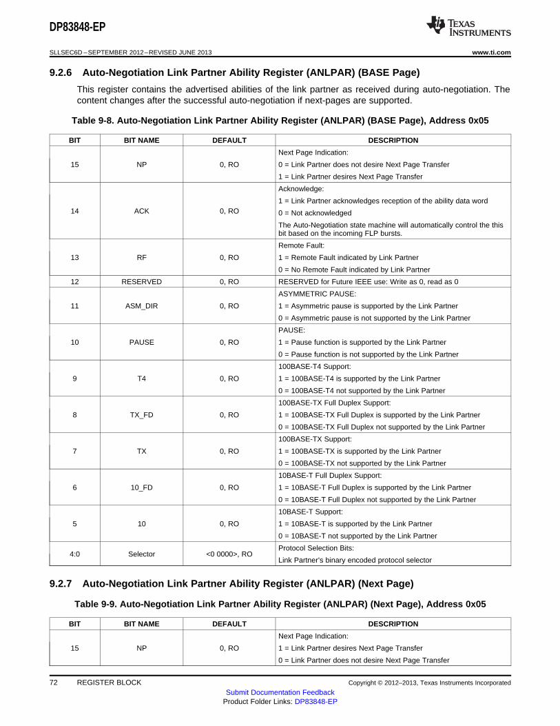
DP83848-EP
SLLSEC6D –SEPTEMBER 2012–REVISED JUNE 2013 www.ti.com
9.2.6 Auto-Negotiation Link Partner Ability Register (ANLPAR) (BASE Page)
This register contains the advertised abilities of the link partner as received during auto-negotiation. Thecontent changes after the successful auto-negotiation if next-pages are supported.
Table 9-8. Auto-Negotiation Link Partner Ability Register (ANLPAR) (BASE Page), Address 0x05
BIT BIT NAME DEFAULT DESCRIPTION
Next Page Indication:
15 NP 0, RO 0 = Link Partner does not desire Next Page Transfer
1 = Link Partner desires Next Page Transfer
Acknowledge:
1 = Link Partner acknowledges reception of the ability data word14 ACK 0, RO 0 = Not acknowledged
The Auto-Negotiation state machine will automatically control the thisbit based on the incoming FLP bursts.
Remote Fault:
13 RF 0, RO 1 = Remote Fault indicated by Link Partner
0 = No Remote Fault indicated by Link Partner
12 RESERVED 0, RO RESERVED for Future IEEE use: Write as 0, read as 0
ASYMMETRIC PAUSE:
11 ASM_DIR 0, RO 1 = Asymmetric pause is supported by the Link Partner
0 = Asymmetric pause is not supported by the Link Partner
PAUSE:
10 PAUSE 0, RO 1 = Pause function is supported by the Link Partner
0 = Pause function is not supported by the Link Partner
100BASE-T4 Support:
9 T4 0, RO 1 = 100BASE-T4 is supported by the Link Partner
0 = 100BASE-T4 not supported by the Link Partner
100BASE-TX Full Duplex Support:
8 TX_FD 0, RO 1 = 100BASE-TX Full Duplex is supported by the Link Partner
0 = 100BASE-TX Full Duplex not supported by the Link Partner
100BASE-TX Support:
7 TX 0, RO 1 = 100BASE-TX is supported by the Link Partner
0 = 100BASE-TX not supported by the Link Partner
10BASE-T Full Duplex Support:
6 10_FD 0, RO 1 = 10BASE-T Full Duplex is supported by the Link Partner
0 = 10BASE-T Full Duplex not supported by the Link Partner
10BASE-T Support:
5 10 0, RO 1 = 10BASE-T is supported by the Link Partner
0 = 10BASE-T not supported by the Link Partner
Protocol Selection Bits:4:0 Selector <0 0000>, RO
Link Partner’s binary encoded protocol selector
9.2.7 Auto-Negotiation Link Partner Ability Register (ANLPAR) (Next Page)
Table 9-9. Auto-Negotiation Link Partner Ability Register (ANLPAR) (Next Page), Address 0x05
BIT BIT NAME DEFAULT DESCRIPTION
Next Page Indication:
15 NP 0, RO 1 = Link Partner desires Next Page Transfer
0 = Link Partner does not desire Next Page Transfer
72 REGISTER BLOCK Copyright © 2012–2013, Texas Instruments Incorporated
Submit Documentation FeedbackProduct Folder Links: DP83848-EP
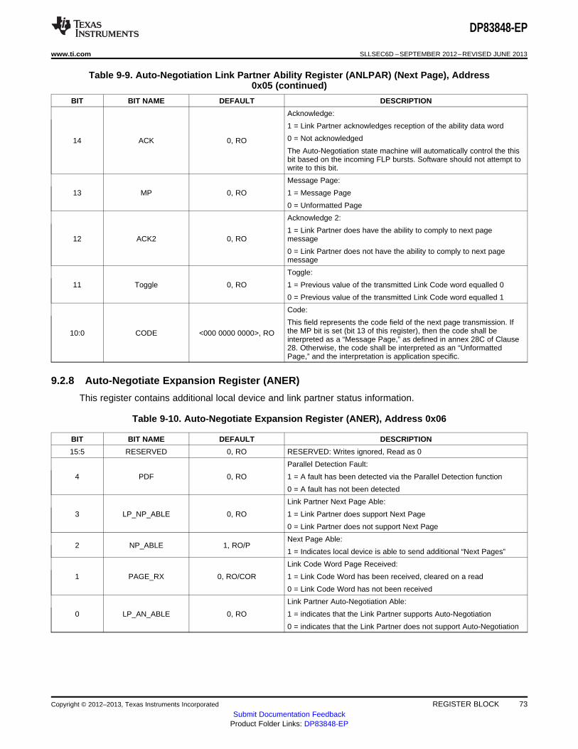
DP83848-EP
www.ti.com SLLSEC6D –SEPTEMBER 2012–REVISED JUNE 2013
Table 9-9. Auto-Negotiation Link Partner Ability Register (ANLPAR) (Next Page), Address0x05 (continued)
BIT BIT NAME DEFAULT DESCRIPTION
Acknowledge:
1 = Link Partner acknowledges reception of the ability data word
0 = Not acknowledged14 ACK 0, ROThe Auto-Negotiation state machine will automatically control the thisbit based on the incoming FLP bursts. Software should not attempt towrite to this bit.
Message Page:
13 MP 0, RO 1 = Message Page
0 = Unformatted Page
Acknowledge 2:
1 = Link Partner does have the ability to comply to next page12 ACK2 0, RO message
0 = Link Partner does not have the ability to comply to next pagemessage
Toggle:
11 Toggle 0, RO 1 = Previous value of the transmitted Link Code word equalled 0
0 = Previous value of the transmitted Link Code word equalled 1
Code:
This field represents the code field of the next page transmission. Ifthe MP bit is set (bit 13 of this register), then the code shall be10:0 CODE <000 0000 0000>, ROinterpreted as a “Message Page,” as defined in annex 28C of Clause28. Otherwise, the code shall be interpreted as an “UnformattedPage,” and the interpretation is application specific.
9.2.8 Auto-Negotiate Expansion Register (ANER)
This register contains additional local device and link partner status information.
Table 9-10. Auto-Negotiate Expansion Register (ANER), Address 0x06
BIT BIT NAME DEFAULT DESCRIPTION
15:5 RESERVED 0, RO RESERVED: Writes ignored, Read as 0
Parallel Detection Fault:
4 PDF 0, RO 1 = A fault has been detected via the Parallel Detection function
0 = A fault has not been detected
Link Partner Next Page Able:
3 LP_NP_ABLE 0, RO 1 = Link Partner does support Next Page
0 = Link Partner does not support Next Page
Next Page Able:2 NP_ABLE 1, RO/P
1 = Indicates local device is able to send additional “Next Pages”
Link Code Word Page Received:
1 PAGE_RX 0, RO/COR 1 = Link Code Word has been received, cleared on a read
0 = Link Code Word has not been received
Link Partner Auto-Negotiation Able:
0 LP_AN_ABLE 0, RO 1 = indicates that the Link Partner supports Auto-Negotiation
0 = indicates that the Link Partner does not support Auto-Negotiation
Copyright © 2012–2013, Texas Instruments Incorporated REGISTER BLOCK 73Submit Documentation Feedback
Product Folder Links: DP83848-EP

DP83848-EP
SLLSEC6D –SEPTEMBER 2012–REVISED JUNE 2013 www.ti.com
9.2.9 Auto-Negotiation Next Page Transmit Register (ANNPTR)
This register contains the next page information sent by this device to its link partner during auto-negotiation.
Table 9-11. Auto-Negotiation Next Page Transmit Register (ANNPTR), Address 0x07
BIT BIT NAME DEFAULT DESCRIPTION
Next Page Indication:
15 NP 0, RW 0 = No other Next Page Transfer desired
1 = Another Next Page desired
14 RESERVED 0, RO RESERVED: Writes ignored, read as 0
Message Page:
13 MP 1, RW 1 = Message Page
0 = Unformatted Page
Acknowledge2:
1 = Will comply with message12 ACK2 0, RW 0 = Cannot comply with message
Acknowledge2 is used by the next page function to indicate that LocalDevice has the ability to comply with the message received.
Toggle:
1 = Value of toggle bit in previously transmitted Link Code Word was 0
0 = Value of toggle bit in previously transmitted Link Code Word was 111 TOG_TX 0, RO
Toggle is used by the Arbitration function within Auto-Negotiation toensure synchronization with the Link Partner during Next Pageexchange. This bit shall always take the opposite value of the Togglebit in the previously exchanged Link Code Word.
This field represents the code field of the next page transmission. If theMP bit is set (bit 13 of this register), then the code shall be interpretedas a "Message Page”, as defined in annex 28C of IEEE 802.3u.Otherwise, the code shall be interpreted as an "Unformatted Page”, and10:0 CODE <000 0000 0001>, RWthe interpretation is application specific.
The default value of the CODE represents a Null Page as defined inAnnex 28C of IEEE 802.3u.
9.3 Extended Registers
9.3.1 PHY Status Register (PHYSTS)
This register provides a single location within the register set for quick access to commonly accessedinformation.
Table 9-12. PHY Status Register (PHYSTS), Address 0x10
BIT BIT NAME DEFAULT DESCRIPTION
15 RESERVED 0, RO RESERVED: Write ignored, read as 0
MDI-X mode as reported by the Auto-Negotiation logic:
This bit will be affected by the settings of the MDIX_EN andFORCE_MDIX bits in the PHYCR register. When MDIX is enabled,but not forced, this bit will update dynamically as the Auto-MDIXalgorithm swaps between MDI and MDI-X configurations.
14 MDI-X Mode 0, RO1 = MDI pairs swapped
(Receive on TPTD pair, Transmit on TPRD pair)
0 = MDI pairs normal
(Receive on TRD pair, Transmit on TPTD pair)
74 REGISTER BLOCK Copyright © 2012–2013, Texas Instruments Incorporated
Submit Documentation FeedbackProduct Folder Links: DP83848-EP
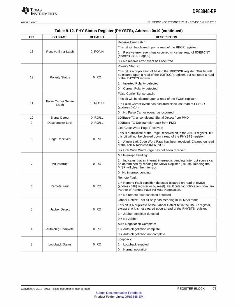
DP83848-EP
www.ti.com SLLSEC6D –SEPTEMBER 2012–REVISED JUNE 2013
Table 9-12. PHY Status Register (PHYSTS), Address 0x10 (continued)
BIT BIT NAME DEFAULT DESCRIPTION
Receive Error Latch:
This bit will be cleared upon a read of the RECR register.13 Receive Error Latch 0, RO/LH 1 = Receive error event has occurred since last read of RXERCNT
(address 0x15, Page 0)
0 = No receive error event has occurred
Polarity Status:
This bit is a duplication of bit 4 in the 10BTSCR register. This bit willbe cleared upon a read of the 10BTSCR register, but not upon a read
12 Polarity Status 0, RO of the PHYSTS register.
1 = Inverted Polarity detected
0 = Correct Polarity detected
False Carrier Sense Latch:
This bit will be cleared upon a read of the FCSR register.False Carrier Sense11 0, RO/LH 1 = False Carrier event has occurred since last read of FCSCRLatch
(address 0x14)
0 = No False Carrier event has occurred
10 Signal Detect 0, RO/LL 100Base-TX unconditional Signal Detect from PMD
9 Descrambler Lock 0, RO/LL 100Base-TX Descrambler Lock from PMD
Link Code Word Page Received:
This is a duplicate of the Page Received bit in the ANER register, butthis bit will not be cleared upon a read of the PHYSTS register.
8 Page Received 0, RO1 = A new Link Code Word Page has been received. Cleared on readof the ANER (address 0x06, bit 1)
0 = Link Code Word Page has not been received
MII Interrupt Pending:
1 = Indicates that an internal interrupt is pending. Interrupt source can7 MII Interrupt 0, RO be determined by reading the MISR Register (0x12h). Reading the
MISR will clear the Interrupt.
0= No interrupt pending
Remote Fault:
1 = Remote Fault condition detected (cleared on read of BMSR6 Remote Fault 0, RO (address 01h) register or by reset). Fault criteria: notification from Link
Partner of Remote Fault via Auto-Negotiation.
0 = No remote fault condition detected
Jabber Detect: This bit only has meaning in 10 Mb/s mode
This bit is a duplicate of the Jabber Detect bit in the BMSR register,except that it is not cleared upon a read of the PHYSTS register.5 Jabber Detect 0, RO1 = Jabber condition detected
0 = No Jabber
Auto-Negotiation Complete:
4 Auto-Neg Complete 0, RO 1 = Auto-Negotiation complete
0 = Auto-Negotiation not complete
Loopback:
3 Loopback Status 0, RO 1 = Loopback enabled
0 = Normal operation
Copyright © 2012–2013, Texas Instruments Incorporated REGISTER BLOCK 75Submit Documentation Feedback
Product Folder Links: DP83848-EP

DP83848-EP
SLLSEC6D –SEPTEMBER 2012–REVISED JUNE 2013 www.ti.com
Table 9-12. PHY Status Register (PHYSTS), Address 0x10 (continued)
BIT BIT NAME DEFAULT DESCRIPTION
Duplex:
This bit indicates duplex status and is determined from Auto-Negotiation or Forced Modes.
1 = Full duplex mode2 Duplex Status 0, RO0 = Half duplex mode
Note: This bit is only valid if Auto-Negotiation is enabled and completeand there is a valid link or if Auto-Negotiation is disabled and there isa valid link.
Speed10:
This bit indicates the status of the speed and is determined from Auto-Negotiation or Forced Modes.
1 = 10 Mb/s mode1 Speed Status 0, RO0 = 100 Mb/s mode
Note: This bit is only valid if Auto-Negotiation is enabled and completeand there is a valid link or if Auto-Negotiation is disabled and there isa valid link.
Link Status:
This bit is a duplicate of the Link Status bit in the BMSR register,except that it will not be cleared upon a read of the PHYSTS register.0 Link Status 0, RO1 = Valid link established (for either 10 or 100 Mb/s operation)
0 = Link not established
9.3.2 MII Interrupt Control Register (MICR)
This register implements the MII interrupt PHY specific control register. Sources for interrupt generationinclude: energy detect state change, link state change, speed status change, duplex status change, auto-negotiation complete or any of the counters becoming half-full. The individual interrupt events must beenabled by setting bits in the MII interrupt status and event control register (MISR).
Table 9-13. MII Interrupt Control Register (MICR), Address 0x11
BIT BIT NAME DEFAULT DESCRIPTION
15:3 RESERVED 0, RO Reserved: Write ignored, Read as 0
Test Interrupt:
Forces the PHY to generate an interrupt to facilitate interrupt testing.Interrupts will continue to be generated as long as this bit remains set.2 TINT 0, RW1 = Generate an interrupt
0 = Do not generate interrupt
Interrupt Enable:
Enable interrupt dependent on the event enables in the MISR register.1 INTEN 0, RW
1 = Enable event based interrupts
0 = Disable event based interrupts
Interrupt Output Enable:
Enable interrupt events to signal via the PWR_DOWN/INT pin byconfiguring the PWR_DOWN/INT pin as an output.0 INT_OE 0, RW1 = PWR_DOWN/INT is an Interrupt Output
0 = PWR_DOWN/INT is a Power Down Input
76 REGISTER BLOCK Copyright © 2012–2013, Texas Instruments Incorporated
Submit Documentation FeedbackProduct Folder Links: DP83848-EP

DP83848-EP
www.ti.com SLLSEC6D –SEPTEMBER 2012–REVISED JUNE 2013
9.3.3 MII Interrupt Status and Miscellaneous Control Register (MISR)
This register contains event status and enables for the interrupt function. If an event has occurred sincethe last read of this register, the corresponding status bit will be set. If the corresponding enable bit in theregister is set, an interrupt will be generated if the event occurs. The MICR register controls must also beset to allow interrupts. The status indications in this register will be set even if the interrupt is not enabled.
Table 9-14. MII Interrupt Status and Miscellaneous Control Register (MISR), Address 0x12
BIT BIT NAME DEFAULT DESCRIPTION
15 RESERVED 0, RO RESERVED: Writes ignored, Read as 0
Energy Detect interrupt:
1 = Energy detect interrupt is pending and is cleared by the current14 ED_INT 0, RO/COR read
0 = No energy detect interrupt pending
Change of Link Status interrupt:
1 = Change of link status interrupt is pending and is cleared by the13 LINK_INT 0, RO/COR current read
0 = No change of link status interrupt pending
Change of speed status interrupt:
1 = Speed status change interrupt is pending and is cleared by the12 SPD_INT 0, RO/COR current read
0 = No speed status change interrupt pending
Change of duplex status interrupt:
1 = Duplex status change interrupt is pending and is cleared by the11 DUP_INT 0, RO/COR current read
0 = No duplex status change interrupt pending
Auto-Negotiation Complete interrupt:
1 = Auto-negotiation complete interrupt is pending and is cleared by10 ANC_INT 0, RO/COR the current read
0 = No Auto-negotiation complete interrupt pending
False Carrier Counter half-full interrupt:
1 = False carrier counter half-full interrupt is pending and is cleared by9 FHF_INT 0, RO/COR the current read
0 = No false carrier counter half-full interrupt pending
Receive Error Counter half-full interrupt:
1 = Receive error counter half-full interrupt is pending and is cleared8 RHF_INT 0, RO/COR by the current read
0 = No receive error carrier counter half-full interrupt pending
7 RESERVED 0, RO RESERVED: Writes ignored, Read as 0
6 ED_INT_EN 0, RW Enable Interrupt on energy detect event
5 LINK_INT_EN 0, RW Enable Interrupt on change of link status
4 SPD_INT_EN 0, RW Enable Interrupt on change of speed status
3 DUP_INT_EN 0, RW Enable Interrupt on change of duplex status
2 ANC_INT_EN 0, RW Enable Interrupt on Auto-negotiation complete event
1 FHF_INT_EN 0, RW Enable Interrupt on False Carrier Counter Register half-full event
0 RHF_INT_EN 0, RW Enable Interrupt on Receive Error Counter Register half-full event
Copyright © 2012–2013, Texas Instruments Incorporated REGISTER BLOCK 77Submit Documentation Feedback
Product Folder Links: DP83848-EP
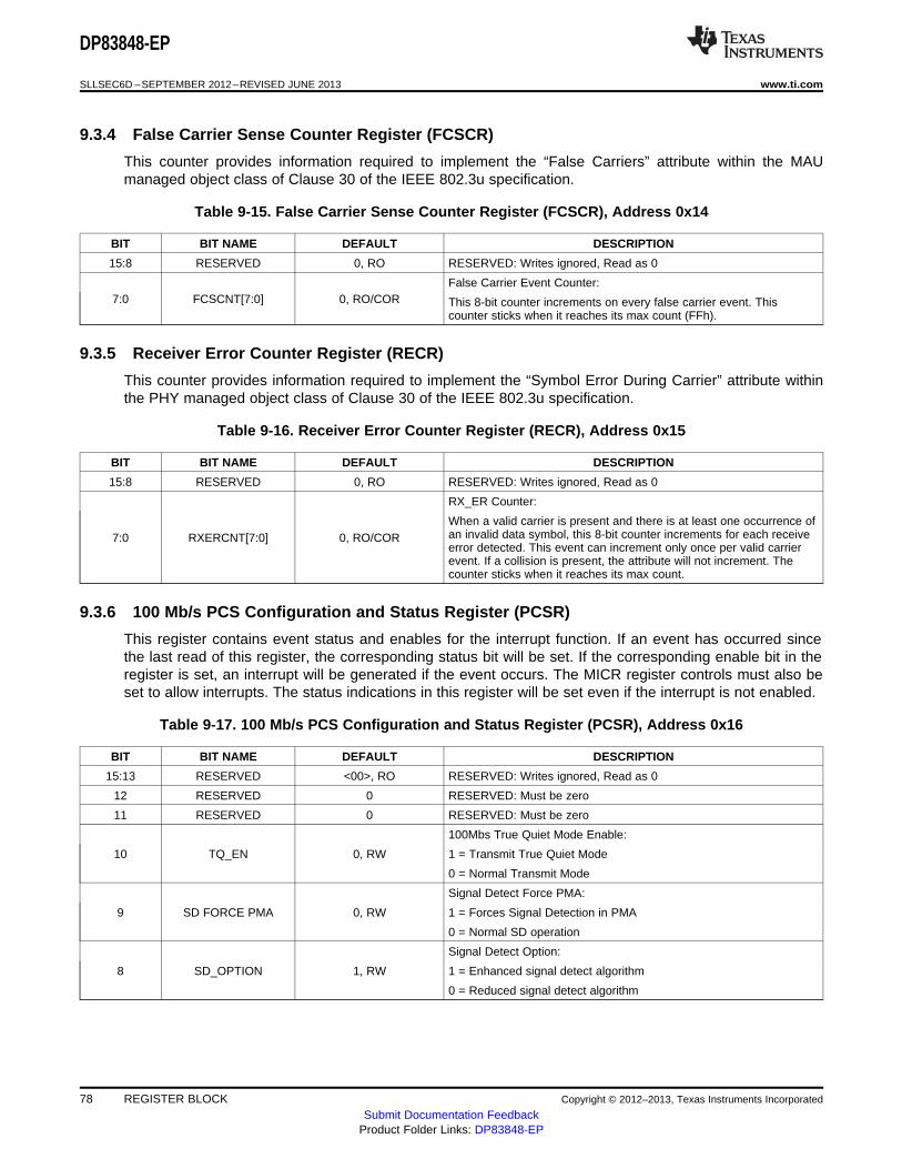
DP83848-EP
SLLSEC6D –SEPTEMBER 2012–REVISED JUNE 2013 www.ti.com
9.3.4 False Carrier Sense Counter Register (FCSCR)
This counter provides information required to implement the “False Carriers” attribute within the MAUmanaged object class of Clause 30 of the IEEE 802.3u specification.
Table 9-15. False Carrier Sense Counter Register (FCSCR), Address 0x14
BIT BIT NAME DEFAULT DESCRIPTION
15:8 RESERVED 0, RO RESERVED: Writes ignored, Read as 0
False Carrier Event Counter:7:0 FCSCNT[7:0] 0, RO/COR This 8-bit counter increments on every false carrier event. This
counter sticks when it reaches its max count (FFh).
9.3.5 Receiver Error Counter Register (RECR)
This counter provides information required to implement the “Symbol Error During Carrier” attribute withinthe PHY managed object class of Clause 30 of the IEEE 802.3u specification.
Table 9-16. Receiver Error Counter Register (RECR), Address 0x15
BIT BIT NAME DEFAULT DESCRIPTION
15:8 RESERVED 0, RO RESERVED: Writes ignored, Read as 0
RX_ER Counter:
When a valid carrier is present and there is at least one occurrence ofan invalid data symbol, this 8-bit counter increments for each receive7:0 RXERCNT[7:0] 0, RO/CORerror detected. This event can increment only once per valid carrierevent. If a collision is present, the attribute will not increment. Thecounter sticks when it reaches its max count.
9.3.6 100 Mb/s PCS Configuration and Status Register (PCSR)
This register contains event status and enables for the interrupt function. If an event has occurred sincethe last read of this register, the corresponding status bit will be set. If the corresponding enable bit in theregister is set, an interrupt will be generated if the event occurs. The MICR register controls must also beset to allow interrupts. The status indications in this register will be set even if the interrupt is not enabled.
Table 9-17. 100 Mb/s PCS Configuration and Status Register (PCSR), Address 0x16
BIT BIT NAME DEFAULT DESCRIPTION
15:13 RESERVED <00>, RO RESERVED: Writes ignored, Read as 0
12 RESERVED 0 RESERVED: Must be zero
11 RESERVED 0 RESERVED: Must be zero
100Mbs True Quiet Mode Enable:
10 TQ_EN 0, RW 1 = Transmit True Quiet Mode
0 = Normal Transmit Mode
Signal Detect Force PMA:
9 SD FORCE PMA 0, RW 1 = Forces Signal Detection in PMA
0 = Normal SD operation
Signal Detect Option:
8 SD_OPTION 1, RW 1 = Enhanced signal detect algorithm
0 = Reduced signal detect algorithm
78 REGISTER BLOCK Copyright © 2012–2013, Texas Instruments Incorporated
Submit Documentation FeedbackProduct Folder Links: DP83848-EP
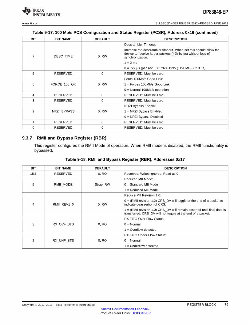
DP83848-EP
www.ti.com SLLSEC6D –SEPTEMBER 2012–REVISED JUNE 2013
Table 9-17. 100 Mb/s PCS Configuration and Status Register (PCSR), Address 0x16 (continued)
BIT BIT NAME DEFAULT DESCRIPTION
Descrambler Timeout:
Increase the descrambler timeout. When set this should allow thedevice to receive larger packets (>9k bytes) without loss of
7 DESC_TIME 0, RW synchronization.
1 = 2 ms
0 = 722 µs (per ANSI X3.263: 1995 (TP-PMD) 7.2.3.3e)
6 RESERVED 0 RESERVED: Must be zero
Force 100Mb/s Good Link:
5 FORCE_100_OK 0, RW 1 = Forces 100Mb/s Good Link
0 = Normal 100Mb/s operation
4 RESERVED 0 RESERVED: Must be zero
3 RESERVED 0 RESERVED: Must be zero
NRZI Bypass Enable:
2 NRZI_BYPASS 0, RW 1 = NRZI Bypass Enabled
0 = NRZI Bypass Disabled
1 RESERVED 0 RESERVED: Must be zero
0 RESERVED 0 RESERVED: Must be zero
9.3.7 RMII and Bypass Register (RBR)
This register configures the RMII Mode of operation. When RMII mode is disabled, the RMII functionality isbypassed.
Table 9-18. RMII and Bypass Register (RBR), Addresses 0x17
BIT BIT NAME DEFAULT DESCRIPTION
15:6 RESERVED 0, RO Reserved: Writes ignored, Read as 0
Reduced MII Mode:
5 RMII_MODE Strap, RW 0 = Standard MII Mode
1 = Reduced MII Mode
Reduce MII Revision 1.0:
0 = (RMII revision 1.2) CRS_DV will toggle at the end of a packet to4 RMII_REV1_0 0, RW indicate deassertion of CRS.
1 = (RMII revision 1.0) CRS_DV will remain asserted until final data istransferred. CRS_DV will not toggle at the end of a packet.
RX FIFO Over Flow Status:
3 RX_OVF_STS 0, RO 0 = Normal
1 = Overflow detected
RX FIFO Under Flow Status:
2 RX_UNF_STS 0, RO 0 = Normal
1 = Underflow detected
Copyright © 2012–2013, Texas Instruments Incorporated REGISTER BLOCK 79Submit Documentation Feedback
Product Folder Links: DP83848-EP
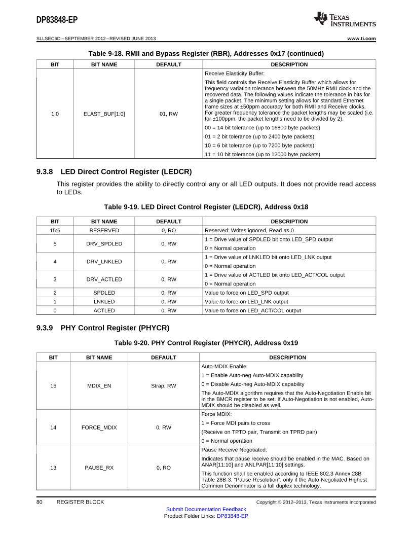
DP83848-EP
SLLSEC6D –SEPTEMBER 2012–REVISED JUNE 2013 www.ti.com
Table 9-18. RMII and Bypass Register (RBR), Addresses 0x17 (continued)
BIT BIT NAME DEFAULT DESCRIPTION
Receive Elasticity Buffer:
This field controls the Receive Elasticity Buffer which allows forfrequency variation tolerance between the 50MHz RMII clock and therecovered data. The following values indicate the tolerance in bits fora single packet. The minimum setting allows for standard Ethernetframe sizes at ±50ppm accuracy for both RMII and Receive clocks.For greater frequency tolerance the packet lengths may be scaled (i.e.1:0 ELAST_BUF[1:0] 01, RWfor ±100ppm, the packet lengths need to be divided by 2).
00 = 14 bit tolerance (up to 16800 byte packets)
01 = 2 bit tolerance (up to 2400 byte packets)
10 = 6 bit tolerance (up to 7200 byte packets)
11 = 10 bit tolerance (up to 12000 byte packets)
9.3.8 LED Direct Control Register (LEDCR)
This register provides the ability to directly control any or all LED outputs. It does not provide read accessto LEDs.
Table 9-19. LED Direct Control Register (LEDCR), Address 0x18
BIT BIT NAME DEFAULT DESCRIPTION
15:6 RESERVED 0, RO Reserved: Writes ignored, Read as 0
1 = Drive value of SPDLED bit onto LED_SPD output5 DRV_SPDLED 0, RW
0 = Normal operation
1 = Drive value of LNKLED bit onto LED_LNK output4 DRV_LNKLED 0, RW
0 = Normal operation
1 = Drive value of ACTLED bit onto LED_ACT/COL output3 DRV_ACTLED 0, RW
0 = Normal operation
2 SPDLED 0, RW Value to force on LED_SPD output
1 LNKLED 0, RW Value to force on LED_LNK output
0 ACTLED 0, RW Value to force on LED_ACT/COL output
9.3.9 PHY Control Register (PHYCR)
Table 9-20. PHY Control Register (PHYCR), Address 0x19
BIT BIT NAME DEFAULT DESCRIPTION
Auto-MDIX Enable:
1 = Enable Auto-neg Auto-MDIX capability
0 = Disable Auto-neg Auto-MDIX capability15 MDIX_EN Strap, RWThe Auto-MDIX algorithm requires that the Auto-Negotiation Enable bitin the BMCR register to be set. If Auto-Negotiation is not enabled, Auto-MDIX should be disabled as well.
Force MDIX:
1 = Force MDI pairs to cross14 FORCE_MDIX 0, RW
(Receive on TPTD pair, Transmit on TPRD pair)
0 = Normal operation
Pause Receive Negotiated:
Indicates that pause receive should be enabled in the MAC. Based onANAR[11:10] and ANLPAR[11:10] settings.13 PAUSE_RX 0, ROThis function shall be enabled according to IEEE 802.3 Annex 28BTable 28B-3, “Pause Resolution”, only if the Auto-Negotiated HighestCommon Denominator is a full duplex technology.
80 REGISTER BLOCK Copyright © 2012–2013, Texas Instruments Incorporated
Submit Documentation FeedbackProduct Folder Links: DP83848-EP
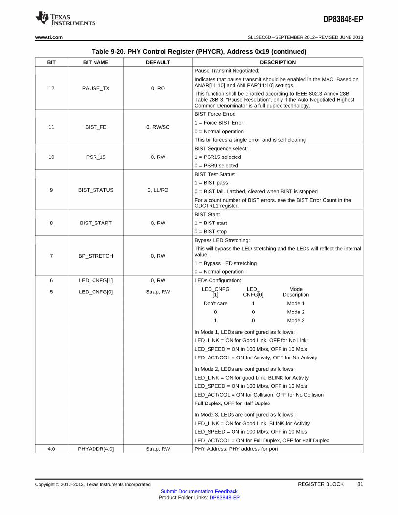
DP83848-EP
www.ti.com SLLSEC6D –SEPTEMBER 2012–REVISED JUNE 2013
Table 9-20. PHY Control Register (PHYCR), Address 0x19 (continued)
BIT BIT NAME DEFAULT DESCRIPTION
Pause Transmit Negotiated:
Indicates that pause transmit should be enabled in the MAC. Based onANAR[11:10] and ANLPAR[11:10] settings.12 PAUSE_TX 0, ROThis function shall be enabled according to IEEE 802.3 Annex 28BTable 28B-3, “Pause Resolution”, only if the Auto-Negotiated HighestCommon Denominator is a full duplex technology.
BIST Force Error:
1 = Force BIST Error11 BIST_FE 0, RW/SC
0 = Normal operation
This bit forces a single error, and is self clearing
BIST Sequence select:
10 PSR_15 0, RW 1 = PSR15 selected
0 = PSR9 selected
BIST Test Status:
1 = BIST pass9 BIST_STATUS 0, LL/RO 0 = BIST fail. Latched, cleared when BIST is stopped
For a count number of BIST errors, see the BIST Error Count in theCDCTRL1 register.
BIST Start:
8 BIST_START 0, RW 1 = BIST start
0 = BIST stop
Bypass LED Stretching:
This will bypass the LED stretching and the LEDs will reflect the internalvalue.7 BP_STRETCH 0, RW1 = Bypass LED stretching
0 = Normal operation
6 LED_CNFG[1] 0, RW LEDs Configuration:
LED_CNFG LED_ Mode5 LED_CNFG[0] Strap, RW [1] CNFG[0] Description
Don’t care 1 Mode 1
0 0 Mode 2
1 0 Mode 3
In Mode 1, LEDs are configured as follows:
LED_LINK = ON for Good Link, OFF for No Link
LED_SPEED = ON in 100 Mb/s, OFF in 10 Mb/s
LED_ACT/COL = ON for Activity, OFF for No Activity
In Mode 2, LEDs are configured as follows:
LED_LINK = ON for good Link, BLINK for Activity
LED_SPEED = ON in 100 Mb/s, OFF in 10 Mb/s
LED_ACT/COL = ON for Collision, OFF for No Collision
Full Duplex, OFF for Half Duplex
In Mode 3, LEDs are configured as follows:
LED_LINK = ON for Good Link, BLINK for Activity
LED_SPEED = ON in 100 Mb/s, OFF in 10 Mb/s
LED_ACT/COL = ON for Full Duplex, OFF for Half Duplex
4:0 PHYADDR[4:0] Strap, RW PHY Address: PHY address for port
Copyright © 2012–2013, Texas Instruments Incorporated REGISTER BLOCK 81Submit Documentation Feedback
Product Folder Links: DP83848-EP

DP83848-EP
SLLSEC6D –SEPTEMBER 2012–REVISED JUNE 2013 www.ti.com
9.3.10 10Base-T Status/Control Register (10BTSCR)
Table 9-21. 10Base-T Status/Control Register (10BTSCR), Address 0x1A
BIT BIT NAME DEFAULT DESCRIPTION
10Base-T Serial Mode (SNI):
1 = Enables 10Base-T Serial Mode
0 = Normal Operation15 10BT_SERIAL Strap, RWPlaces 10 Mb/s transmit and receive functions in Serial NetworkInterface (SNI) Mode of operation. Has no effect on 100 Mb/soperation.
14:12 RESERVED 0, RW RESERVED: Must be zero
Squelch Configuration:
11:9 SQUELCH 100, RW Used to set the Squelch ‘ON’ threshold for the receiver
Default Squelch ON is 330mV peak
In half-duplex mode, default 10BASE-T operation loops Transmit datato the Receive data in addition to transmitting the data on the physicalmedium. This is for consistency with earlier 10BASE2 and 10BASE5
8 LOOPBACK_10_D IS 0, RW implementations which used a shared medium. Setting this bitdisables the loopback function.
This bit does not affect loopback due to setting BMCR[14].
Normal Link Pulse Disable:
7 LP_DIS 0, RW 1 = Transmission of NLPs is disabled
0 = Transmission of NLPs is enabled
Force 10Mb Good Link:
6 FORCE_LINK_10 0, RW 1 = Forced Good 10Mb Link
0 = Normal Link Status
5 RESERVED 0, RW RESERVED: Must be zero
10Mb Polarity Status:
This bit is a duplication of bit 12 in the PHYSTS register. Both bits willbe cleared upon a read of 10BTSCR register, but not upon a read of
4 POLARITY RO/LH the PHYSTS register.
1 = Inverted Polarity detected
0 = Correct Polarity detected
3 RESERVED 0, RW RESERVED: Must be zero
2 RESERVED 1, RW RESERVED: Must be zero
Heartbeat Disable: This bit only has influence in half-duplex 10Mbmode.
1 = Heartbeat function disabled1 HEARTBEAT_DIS 0, RW
0 = Heartbeat function enabled
When the device is operating at 100Mb or configured for full duplexoperation, this bit will be ignored - the heartbeat function is disabled.
Jabber Disable:
Applicable only in 10BASE-T.0 JABBER_DIS 0, RW
1 = Jabber function disabled
0 = Jabber function enabled
82 REGISTER BLOCK Copyright © 2012–2013, Texas Instruments Incorporated
Submit Documentation FeedbackProduct Folder Links: DP83848-EP
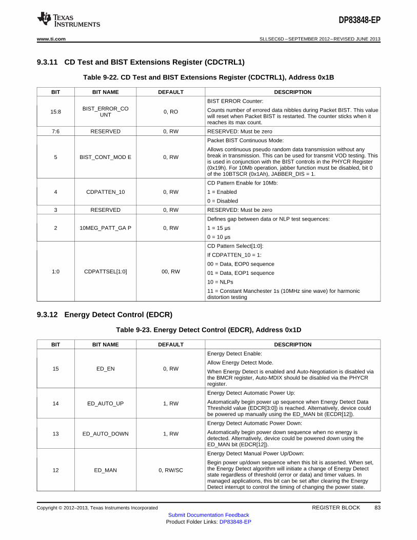
DP83848-EP
www.ti.com SLLSEC6D –SEPTEMBER 2012–REVISED JUNE 2013
9.3.11 CD Test and BIST Extensions Register (CDCTRL1)
Table 9-22. CD Test and BIST Extensions Register (CDCTRL1), Address 0x1B
BIT BIT NAME DEFAULT DESCRIPTION
BIST ERROR Counter:BIST_ERROR_CO Counts number of errored data nibbles during Packet BIST. This value15:8 0, ROUNT will reset when Packet BIST is restarted. The counter sticks when it
reaches its max count.
7:6 RESERVED 0, RW RESERVED: Must be zero
Packet BIST Continuous Mode:
Allows continuous pseudo random data transmission without anybreak in transmission. This can be used for transmit VOD testing. This5 BIST_CONT_MOD E 0, RWis used in conjunction with the BIST controls in the PHYCR Register(0x19h). For 10Mb operation, jabber function must be disabled, bit 0of the 10BTSCR (0x1Ah), JABBER_DIS = 1.
CD Pattern Enable for 10Mb:
4 CDPATTEN_10 0, RW 1 = Enabled
0 = Disabled
3 RESERVED 0, RW RESERVED: Must be zero
Defines gap between data or NLP test sequences:
2 10MEG_PATT_GA P 0, RW 1 = 15 μs
0 = 10 μs
CD Pattern Select[1:0]:
If CDPATTEN_10 = 1:
00 = Data, EOP0 sequence1:0 CDPATTSEL[1:0] 00, RW 01 = Data, EOP1 sequence
10 = NLPs
11 = Constant Manchester 1s (10MHz sine wave) for harmonicdistortion testing
9.3.12 Energy Detect Control (EDCR)
Table 9-23. Energy Detect Control (EDCR), Address 0x1D
BIT BIT NAME DEFAULT DESCRIPTION
Energy Detect Enable:
Allow Energy Detect Mode.15 ED_EN 0, RW When Energy Detect is enabled and Auto-Negotiation is disabled via
the BMCR register, Auto-MDIX should be disabled via the PHYCRregister.
Energy Detect Automatic Power Up:
Automatically begin power up sequence when Energy Detect Data14 ED_AUTO_UP 1, RWThreshold value (EDCR[3:0]) is reached. Alternatively, device couldbe powered up manually using the ED_MAN bit (ECDR[12]).
Energy Detect Automatic Power Down:
Automatically begin power down sequence when no energy is13 ED_AUTO_DOWN 1, RWdetected. Alternatively, device could be powered down using theED_MAN bit (EDCR[12]).
Energy Detect Manual Power Up/Down:
Begin power up/down sequence when this bit is asserted. When set,the Energy Detect algorithm will initiate a change of Energy Detect12 ED_MAN 0, RW/SCstate regardless of threshold (error or data) and timer values. Inmanaged applications, this bit can be set after clearing the EnergyDetect interrupt to control the timing of changing the power state.
Copyright © 2012–2013, Texas Instruments Incorporated REGISTER BLOCK 83Submit Documentation Feedback
Product Folder Links: DP83848-EP
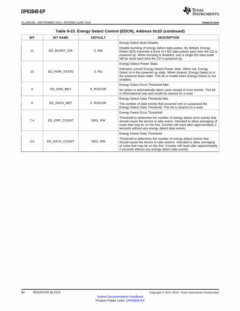
DP83848-EP
SLLSEC6D –SEPTEMBER 2012–REVISED JUNE 2013 www.ti.com
Table 9-23. Energy Detect Control (EDCR), Address 0x1D (continued)
BIT BIT NAME DEFAULT DESCRIPTION
Energy Detect Bust Disable:
Disable bursting of energy detect data pulses. By default, Energy11 ED_BURST_DIS 0, RW Detect (ED) transmits a burst of 4 ED data pulses each time the CD is
powered up. When bursting is disabled, only a single ED data pulsewill be send each time the CD is powered up.
Energy Detect Power State:
Indicates current Energy Detect Power state. When set, Energy10 ED_PWR_STATE 0, RO Detect is in the powered up state. When cleared, Energy Detect is in
the powered down state. This bit is invalid when Energy Detect is notenabled.
Energy Detect Error Threshold Met:9 ED_ERR_MET 0, RO/COR No action is automatically taken upon receipt of error events. This bit
is informational only and would be cleared on a read.
Energy Detect Data Threshold Met:8 ED_DATA_MET 0, RO/COR The number of data events that occurred met or surpassed the
Energy Detect Data Threshold. This bit is cleared on a read.
Energy Detect Error Threshold:
Threshold to determine the number of energy detect error events that7:4 ED_ERR_COUNT 0001, RW should cause the device to take action. Intended to allow averaging of
noise that may be on the line. Counter will reset after approximately 2seconds without any energy detect data events.
Energy Detect Data Threshold:
Threshold to determine the number of energy detect events that3:0 ED_DATA_COUNT 0001, RW should cause the device to take actions. Intended to allow averaging
of noise that may be on the line. Counter will reset after approximately2 seconds without any energy detect data events.
84 REGISTER BLOCK Copyright © 2012–2013, Texas Instruments Incorporated
Submit Documentation FeedbackProduct Folder Links: DP83848-EP
PACKAGE OPTION ADDENDUM
www.ti.com 3-May-2013
Addendum-Page 1
PACKAGING INFORMATION
Orderable Device Status(1)
Package Type PackageDrawing
Pins PackageQty
Eco Plan(2)
Lead/Ball Finish MSL Peak Temp(3)
Op Temp (°C) Top-Side Markings(4)
Samples
DP83848MPHPEP ACTIVE HTQFP PHP 48 250 Green (RoHS& no Sb/Br)
CU NIPDAU Level-4-260C-72 HR -55 to 125 DP83848EP
DP83848MPHPREP ACTIVE HTQFP PHP 48 1000 Green (RoHS& no Sb/Br)
CU NIPDAU Level-4-260C-72 HR -55 to 125 DP83848EP
V62/12615-01XE ACTIVE HTQFP PHP 48 1000 Green (RoHS& no Sb/Br)
CU NIPDAU Level-4-260C-72 HR -55 to 125 DP83848EP
V62/12615-01XE-R ACTIVE HTQFP PHP 48 250 Green (RoHS& no Sb/Br)
CU NIPDAU Level-4-260C-72 HR -55 to 125 DP83848EP
(1) The marketing status values are defined as follows:ACTIVE: Product device recommended for new designs.LIFEBUY: TI has announced that the device will be discontinued, and a lifetime-buy period is in effect.NRND: Not recommended for new designs. Device is in production to support existing customers, but TI does not recommend using this part in a new design.PREVIEW: Device has been announced but is not in production. Samples may or may not be available.OBSOLETE: TI has discontinued the production of the device.
(2) Eco Plan - The planned eco-friendly classification: Pb-Free (RoHS), Pb-Free (RoHS Exempt), or Green (RoHS & no Sb/Br) - please check http://www.ti.com/productcontent for the latest availabilityinformation and additional product content details.TBD: The Pb-Free/Green conversion plan has not been defined.Pb-Free (RoHS): TI's terms "Lead-Free" or "Pb-Free" mean semiconductor products that are compatible with the current RoHS requirements for all 6 substances, including the requirement thatlead not exceed 0.1% by weight in homogeneous materials. Where designed to be soldered at high temperatures, TI Pb-Free products are suitable for use in specified lead-free processes.Pb-Free (RoHS Exempt): This component has a RoHS exemption for either 1) lead-based flip-chip solder bumps used between the die and package, or 2) lead-based die adhesive used betweenthe die and leadframe. The component is otherwise considered Pb-Free (RoHS compatible) as defined above.Green (RoHS & no Sb/Br): TI defines "Green" to mean Pb-Free (RoHS compatible), and free of Bromine (Br) and Antimony (Sb) based flame retardants (Br or Sb do not exceed 0.1% by weightin homogeneous material)
(3) MSL, Peak Temp. -- The Moisture Sensitivity Level rating according to the JEDEC industry standard classifications, and peak solder temperature.
(4) Multiple Top-Side Markings will be inside parentheses. Only one Top-Side Marking contained in parentheses and separated by a "~" will appear on a device. If a line is indented then it is acontinuation of the previous line and the two combined represent the entire Top-Side Marking for that device.
Important Information and Disclaimer:The information provided on this page represents TI's knowledge and belief as of the date that it is provided. TI bases its knowledge and belief on informationprovided by third parties, and makes no representation or warranty as to the accuracy of such information. Efforts are underway to better integrate information from third parties. TI has taken andcontinues to take reasonable steps to provide representative and accurate information but may not have conducted destructive testing or chemical analysis on incoming materials and chemicals.TI and TI suppliers consider certain information to be proprietary, and thus CAS numbers and other limited information may not be available for release.
In no event shall TI's liability arising out of such information exceed the total purchase price of the TI part(s) at issue in this document sold by TI to Customer on an annual basis.

PACKAGE OPTION ADDENDUM
www.ti.com 3-May-2013
Addendum-Page 2

TAPE AND REEL INFORMATION
*All dimensions are nominal
Device PackageType
PackageDrawing
Pins SPQ ReelDiameter
(mm)
ReelWidth
W1 (mm)
A0(mm)
B0(mm)
K0(mm)
P1(mm)
W(mm)
Pin1Quadrant
DP83848MPHPREP HTQFP PHP 48 1000 330.0 16.4 9.3 9.3 2.2 12.0 16.0 Q2
PACKAGE MATERIALS INFORMATION
www.ti.com 13-Jul-2013
Pack Materials-Page 1

*All dimensions are nominal
Device Package Type Package Drawing Pins SPQ Length (mm) Width (mm) Height (mm)
DP83848MPHPREP HTQFP PHP 48 1000 367.0 367.0 38.0
PACKAGE MATERIALS INFORMATION
www.ti.com 13-Jul-2013
Pack Materials-Page 2


IMPORTANT NOTICE
Texas Instruments Incorporated and its subsidiaries (TI) reserve the right to make corrections, enhancements, improvements and otherchanges to its semiconductor products and services per JESD46, latest issue, and to discontinue any product or service per JESD48, latestissue. Buyers should obtain the latest relevant information before placing orders and should verify that such information is current andcomplete. All semiconductor products (also referred to herein as “components”) are sold subject to TI’s terms and conditions of salesupplied at the time of order acknowledgment.
TI warrants performance of its components to the specifications applicable at the time of sale, in accordance with the warranty in TI’s termsand conditions of sale of semiconductor products. Testing and other quality control techniques are used to the extent TI deems necessaryto support this warranty. Except where mandated by applicable law, testing of all parameters of each component is not necessarilyperformed.
TI assumes no liability for applications assistance or the design of Buyers’ products. Buyers are responsible for their products andapplications using TI components. To minimize the risks associated with Buyers’ products and applications, Buyers should provideadequate design and operating safeguards.
TI does not warrant or represent that any license, either express or implied, is granted under any patent right, copyright, mask work right, orother intellectual property right relating to any combination, machine, or process in which TI components or services are used. Informationpublished by TI regarding third-party products or services does not constitute a license to use such products or services or a warranty orendorsement thereof. Use of such information may require a license from a third party under the patents or other intellectual property of thethird party, or a license from TI under the patents or other intellectual property of TI.
Reproduction of significant portions of TI information in TI data books or data sheets is permissible only if reproduction is without alterationand is accompanied by all associated warranties, conditions, limitations, and notices. TI is not responsible or liable for such altereddocumentation. Information of third parties may be subject to additional restrictions.
Resale of TI components or services with statements different from or beyond the parameters stated by TI for that component or servicevoids all express and any implied warranties for the associated TI component or service and is an unfair and deceptive business practice.TI is not responsible or liable for any such statements.
Buyer acknowledges and agrees that it is solely responsible for compliance with all legal, regulatory and safety-related requirementsconcerning its products, and any use of TI components in its applications, notwithstanding any applications-related information or supportthat may be provided by TI. Buyer represents and agrees that it has all the necessary expertise to create and implement safeguards whichanticipate dangerous consequences of failures, monitor failures and their consequences, lessen the likelihood of failures that might causeharm and take appropriate remedial actions. Buyer will fully indemnify TI and its representatives against any damages arising out of the useof any TI components in safety-critical applications.
In some cases, TI components may be promoted specifically to facilitate safety-related applications. With such components, TI’s goal is tohelp enable customers to design and create their own end-product solutions that meet applicable functional safety standards andrequirements. Nonetheless, such components are subject to these terms.
No TI components are authorized for use in FDA Class III (or similar life-critical medical equipment) unless authorized officers of the partieshave executed a special agreement specifically governing such use.
Only those TI components which TI has specifically designated as military grade or “enhanced plastic” are designed and intended for use inmilitary/aerospace applications or environments. Buyer acknowledges and agrees that any military or aerospace use of TI componentswhich have not been so designated is solely at the Buyer's risk, and that Buyer is solely responsible for compliance with all legal andregulatory requirements in connection with such use.
TI has specifically designated certain components as meeting ISO/TS16949 requirements, mainly for automotive use. In any case of use ofnon-designated products, TI will not be responsible for any failure to meet ISO/TS16949.
Products Applications
Audio www.ti.com/audio Automotive and Transportation www.ti.com/automotive
Amplifiers amplifier.ti.com Communications and Telecom www.ti.com/communications
Data Converters dataconverter.ti.com Computers and Peripherals www.ti.com/computers
DLP® Products www.dlp.com Consumer Electronics www.ti.com/consumer-apps
DSP dsp.ti.com Energy and Lighting www.ti.com/energy
Clocks and Timers www.ti.com/clocks Industrial www.ti.com/industrial
Interface interface.ti.com Medical www.ti.com/medical
Logic logic.ti.com Security www.ti.com/security
Power Mgmt power.ti.com Space, Avionics and Defense www.ti.com/space-avionics-defense
Microcontrollers microcontroller.ti.com Video and Imaging www.ti.com/video
RFID www.ti-rfid.com
OMAP Applications Processors www.ti.com/omap TI E2E Community e2e.ti.com
Wireless Connectivity www.ti.com/wirelessconnectivity
Mailing Address: Texas Instruments, Post Office Box 655303, Dallas, Texas 75265Copyright © 2013, Texas Instruments Incorporated

Mouser Electronics
Authorized Distributor
Click to View Pricing, Inventory, Delivery & Lifecycle Information: Texas Instruments:
DP83848MPHPREP DP83848MPHPEP V62/12615-01XE V62/12615-01XE-R