Physical design issues for very large ATM switching systems
12
IEEE JOURNAL ON SELECTED AREAS IN COMMUNICATIONS, VOL. 9, NO. 8, OCTOBER 1991 1227 Physical Design Issues for Very Large ATM Switching Systems Thomas C. Banwell, Member, IEEE, RenCe C. Estes, Sarry F. Habiby, Member, IEEE, Gary A. Hayward, Thomas K. Helstem, Gail R. Lalk, Member, ZEEE, Derek D. Mahoney, Donald K. Wilson, Member, IEEE, and Kenneth C. Young, Jr., Senior Member, IEEE Abstract-Widespread deployment of broadband services may increase the switching capacity requirements of central office switching systems to 1 Tb/s or more. To support this two-to- three-orders-of-magnitude increase in throughput and the ac- companying increase in complexity, new physical design alter- natives that provide rich, high-speed connectivity, excellent thermal management charactei-istics, and high reliability will be needed. In this paper, we examine the physical design issues associated with terabit /second switching systems, particularly with regard to the customer access portion of the switch. We determine the physical design requirements in the areas of backplane interconnections, integrated circuit packaging, and circuit board technology. We also identify areas where existing or near-future physical design technologies are inadequate to meet the requirements of this application. Finally, we consider system-level consequences of our physical model such as power and reliability. I. INTRODUCTION HE anticipated widespread deployment of optical T fiber-based broadband networks and services will cre- ate the need for central office switching systems whose capacity and complexity are much greater than today’s local digital switches. We assume that these broadband switches will have to be scalable to serve the same num- ber of customers (- 100 000 lines maximum) as current switches. Subscriber access to these switches will be at the SONET OC-3 (155.52 Mb/s) or OC-12 (622.08 Mb/s) rate. Therefore, the total bandwidth at the cus- tomer interface to a large switch could be 10 Tb/s or more and, even with a 10: 1 concentration ratio between the customer interface and the core switch fabric, the switch throughput could be 1 Tb/s or more. The interface band- width and fabric throughput are factors of 200 or more greater than existing switches. Further, the call process- ing capabilities of such a switch will have to be more so- phisticated to handle the variety of services and increased calling rates that we can expect with broadband networks. Manuscript received January 1991; revised May 7, 1991. This paper was presented in part at the IEEE Global Telecommunications Conference, San Diego, CA, December 2-5, 1990. T. C. Banwell, R. C. Estes, G. R. Lalk, D. K. Wilson, andK. C. Young, Jr. are with Bellcore, Morristown, NJ 07950. S. F. Habiby, G. A. Hayward, T. K. Helstem, and D. D. Mahoney are with Bellcore, Red Bank, NJ 07701. IEEE Log Number 9101969. SONETIATM SONETI Fabric Module Fig. 1. Next-generation switch (NGS) functional architecture Many of the optical and electrical components neces- sary to realize a large ATM switch have been demon- strated, either individually or integrated into relatively small (< 100 lines) switch prototypes. Whether this hard- ware can be scaled to provide switches with 1 Tb/s or more of throughput will be decided, in large part, by the capabilities of interconnection and packaging technology. This is true both because these technologies will deter- mine if the performance of individual components can be maintained when many of them are integrated into a com- plex system and also because these technologies will be important elements in the economics of large ATM switches. We have performed an analysis of a broadband ATM switch with terabit /second throughput to quantify its interconnection and packaging technology require- ments, and to suggest areas where additional research would lead to system advantages. This analysis also pro- vides a framework within which we assess some system- level consequences of very large ATM switches. The customer interface to such a large ATM switching system will, as in current-generation switches, dominate the switch in terms of size, power consumption, and cost. Therefore, our analysis consists of a “paper” design of a customer interface from which we identify some of the important physical design issues. Although the analysis is 0733-87 16/91 / 1000- 1227$01 .OO 0 199 1 IEEE
Transcript of Physical design issues for very large ATM switching systems
IEEE JOURNAL ON SELECTED AREAS IN COMMUNICATIONS, VOL. 9, NO. 8, OCTOBER 1991 1227
Physical Design Issues for Very Large ATM Switching Systems
Thomas C. Banwell, Member, IEEE, RenCe C . Estes, Sarry F . Habiby, Member, IEEE, Gary A . Hayward, Thomas K. Helstem, Gail R. Lalk, Member, ZEEE, Derek D. Mahoney, Donald K. Wilson, Member, IEEE,
and Kenneth C. Young, Jr . , Senior Member, IEEE
Abstract-Widespread deployment of broadband services may increase the switching capacity requirements of central office switching systems to 1 Tb/s or more. To support this two-to- three-orders-of-magnitude increase in throughput and the ac- companying increase in complexity, new physical design alter- natives that provide rich, high-speed connectivity, excellent thermal management charactei-istics, and high reliability will be needed. In this paper, we examine the physical design issues associated with terabit /second switching systems, particularly with regard to the customer access portion of the switch. We determine the physical design requirements in the areas of backplane interconnections, integrated circuit packaging, and circuit board technology. We also identify areas where existing or near-future physical design technologies are inadequate to meet the requirements of this application. Finally, we consider system-level consequences of our physical model such as power and reliability.
I. INTRODUCTION
HE anticipated widespread deployment of optical T fiber-based broadband networks and services will cre- ate the need for central office switching systems whose capacity and complexity are much greater than today’s local digital switches. We assume that these broadband switches will have to be scalable to serve the same num- ber of customers ( - 100 000 lines maximum) as current switches. Subscriber access to these switches will be at the SONET OC-3 (155.52 Mb/s) or OC-12 (622.08 Mb/s) rate. Therefore, the total bandwidth at the cus- tomer interface to a large switch could be 10 Tb/s or more and, even with a 10: 1 concentration ratio between the customer interface and the core switch fabric, the switch throughput could be 1 Tb/s or more. The interface band- width and fabric throughput are factors of 200 or more greater than existing switches. Further, the call process- ing capabilities of such a switch will have to be more so- phisticated to handle the variety of services and increased calling rates that we can expect with broadband networks.
Manuscript received January 1991; revised May 7, 1991. This paper was presented in part at the IEEE Global Telecommunications Conference, San Diego, CA, December 2-5, 1990.
T. C. Banwell, R. C. Estes, G. R. Lalk, D. K . Wilson, andK. C. Young, Jr. are with Bellcore, Morristown, NJ 07950. S. F. Habiby, G. A . Hayward, T. K . Helstem, and D. D. Mahoney are
with Bellcore, Red Bank, NJ 07701. IEEE Log Number 9101969.
SONETIATM
SONETI Fabric Module
Fig. 1 . Next-generation switch (NGS) functional architecture
Many of the optical and electrical components neces- sary to realize a large ATM switch have been demon- strated, either individually or integrated into relatively small (< 100 lines) switch prototypes. Whether this hard- ware can be scaled to provide switches with 1 Tb/s or more of throughput will be decided, in large part, by the capabilities of interconnection and packaging technology. This is true both because these technologies will deter- mine if the performance of individual components can be maintained when many of them are integrated into a com- plex system and also because these technologies will be important elements in the economics of large ATM switches. We have performed an analysis of a broadband ATM switch with terabit /second throughput to quantify its interconnection and packaging technology require- ments, and to suggest areas where additional research would lead to system advantages. This analysis also pro- vides a framework within which we assess some system- level consequences of very large ATM switches.
The customer interface to such a large ATM switching system will, as in current-generation switches, dominate the switch in terms of size, power consumption, and cost. Therefore, our analysis consists of a “paper” design of a customer interface from which we identify some of the important physical design issues. Although the analysis is
0733-87 16/91 / 1000- 1227$01 .OO 0 199 1 IEEE
1228 IEEE JOURNAL ON SELECTED AREAS IN COMMUNICATIONS, VOL. 9. NO. 8. OCTOBER 1991
specific to the customer interface, many of the same is- sues will be encountered in other parts of the switch, par- ticularly in the core switching fabric.
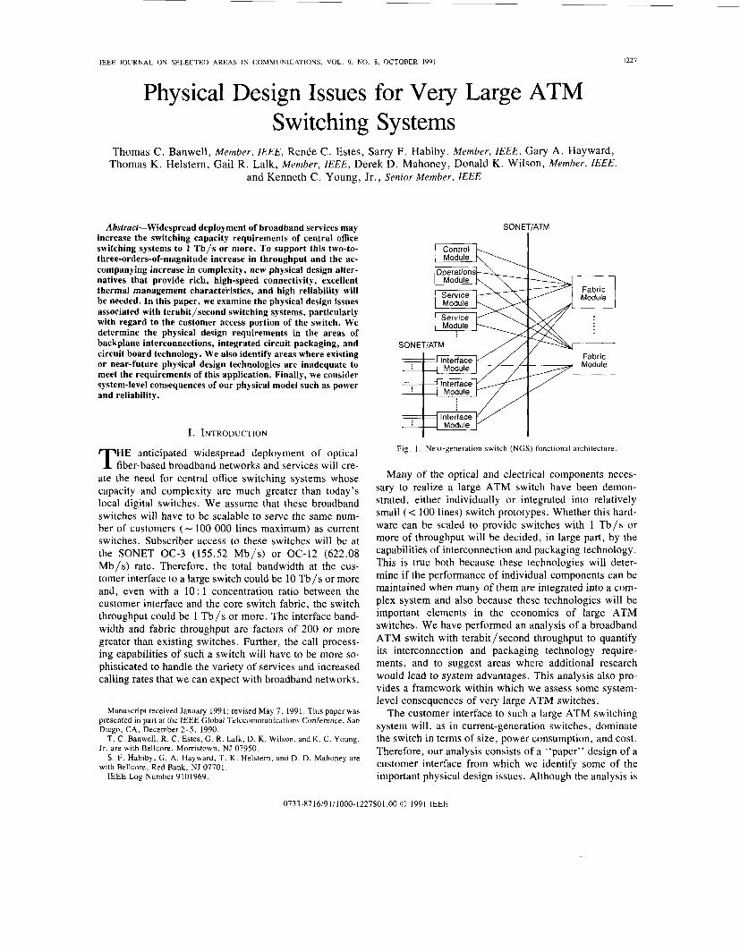
The framework architecture on which the physical de- sign analysis is based is the Bellcore next generation switch (NGS) functional architecture [l]. The NGS ar- chitecture is a modular architecture in which the interface, control, operations, and switching functions are separated into individual modules that together provide a high- speed, large-throughput switching system. A block dia- gram of the basic components is shown in Fig. l . Cus- tomer signaling and traffic are received and transmitted through the interface modules (IM), and are switched through the fabric modules (FM) for service capabilities defined under the instruction of the control, operations, and service modules (CM, OM, and SM, respectively). As shown in Fig. 1, open interfaces using SONETIATM are used to interconnect the modules of the NGS.
11. INTERFACE MODULE MODEL To quantify the physical design issues associated with
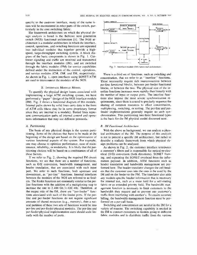
implementing a large ATM switching system, we have performed a “paper” design of the NGS interface module (IM). Fig. 2 shows a functional diagram of this module. Internal paths shown by solid lines carry data in the form of ATM cells (these may be in some proprietary format since they are internal to a module). Dotted lines repre- sent communication paths of internal control and opera- tions information that may use different protocols.
A . Partitioning The basis of any physical design is the system parti-
tioning. Some of the choices that have to be made at the beginning of the design are based on the optimization of various functional aspects of the system. For example, one may choose to optimize performance, ease of main- tenance, reliability, or modularity. It is likely that the par- titioning choices will be based on a combination of all of these factors.
If we refer to Fig. 2, showing the required IM circuit functions, we see that there are a number of functions, such as O/E conversion, bandwidth management, and header translation, that are associated with each input port. We refer to such functions, both upstream and downstream, as ‘ ‘per-line’’ functions. Internal interfaces between the modules of the NGS are referred to as feed- ers. The feeder functions are essentially similar to the per- line functions with the addition of a multiplexing step to increase the rate to 2.488 Gb/s (OC-48). Therefore, at the output side of the IM, there are “per-feeder’’ func- tions associated with each of the feeder ports. If the per- line and per-feeder functions do not require significant amounts of shared resources (e.g., memory), then a nat- ural partition of these two sets of functions would be into per-line and per-feeder physical modules. The per-line and per-feeder physical implementation sizes should scale lin- early with the number of ports.
Customer Interface Y1
Feeder lntelfam -- - Y1
* c
Internal Routing a
COnCentralion Cunomer Interface YN
XM Bandwidth Management
Header Translation a -
A-- 4
Fig. 2. Interface module (IM) functional architecture
There is a third set of functions, such as switching and concentration, that we refer to as “interline” functions. These necessarily require rich interconnection between per-line functional blocks, between per-feeder functional blocks, or between the two. The physical size of the in- terline functions increases more rapidly than linearly with the number of input or output ports. The interline func- tions also impose the most severe synchronization re- quirements, since there is a need to precisely sequence the sharing of common resources to effect concentration, multiplexing, switching, or sorting. The per-line and per- feeder implementations generally require no such syn- chronization. This partitioning into three functional types is the basis for the IM physical model discussed next.
B. IM Functional Architecture With the above as background, we can analyze a phys-
ical architecture of the IM. The purpose of this analysis is not to present a specific IM architecture, but rather to describe a realistic framework from which physical de- sign problems can be analyzed.
As shown in Fig. 2, the customer interface terminates a customer’s fibers and is responsible for optical-to-elec- trical (O/E) conversion (both directions), SONET fram- ing, and separating the SONET overhead from the infor- mation payload. In addition, ATM functions such as header translation and bandwidth management are per- formed here. The header translator changes the cell head- ers that the customer uses into the ones to be used by the IM and on the feeder to the FM. The translator also adds any module-specific header information that is necessary for internal use, such as a route field for a self-routing fabric or an extended priority field. The bandwidth man- agement function is necessary to limit customers to the bandwidth they request and to prevent one customer’s traffic from interfering with another’s. To ensure accurate billing, the bandwidth management function must be per- formed on a per-call basis.
Switching and concentration are needed in the IM for a variety of reasons. The switching capability is needed in the IM to connect customers to feeders going to different fabric modules and to distribute traffic from the various
BANWELL er al.: VERY LARGE ATM SWITCHING SYSTEMS 1229
r 1
-: 16 -SONET
TolFrom SONET Interline
cilities among many customers. For an initial residential 15’ Mbis Processing Functions
feeders to the customers. Concentration is necessary to share the relatively expensive FM ports and network fa-
-E::::- 16: l SONET+ Demux
Framer 1
- Timing nput Header system, an overall concentration ratio of approximately *Recovery k L e r M P r o c e s s o r H FIFO k 1 5 5 ~ b i s
10: 1 seems reasonable. The IM control and operations functions shown in the figure are needed to interface with the NGS control module and operations module as well as to perform any local control and operations functions.
Line Card 1 Controller H ~ e m o ~ l
Fig. 3 . Block diagram of per-line functions.
-: 49 -Buffer::::- 64 Buffer SONET-
Framer
C. Implementation of IM Functions
16:l SONET+ Demux
155 Mbls
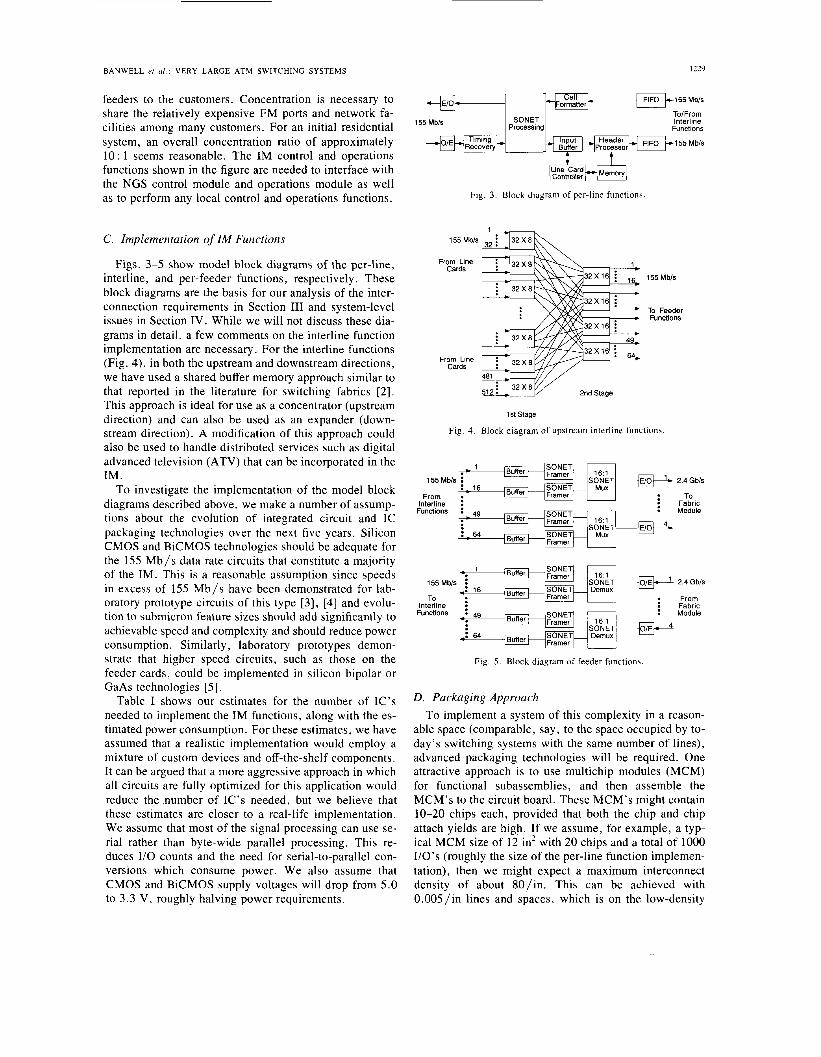
From Line Cards Figs. 3-5 show model block diagrams of the per-line,
interline, and per-feeder functions, respectively. These 155 Mbls
block diagrams are the basis for our analysis of the inter- connection requirements in Section I11 and system-level issues in Section IV. While we will not discuss these dia- grams in detail, a few comments on the interline function implementation are necessary. For the interline functions
we have used a shared buffer memory approach similar to that reported in the literature for switching fabrics [ 2 ] . This approach is ideal for use as a concentrator (upstream direction) and can also be used as an expander (down- stream direction). A modification of this approach could also be used to handle distributed services such as digital
To Feeder Functions
From Line Cards (Fig. 4), in both the upstream and downstream directions,
1 st Stage
Fig. 4. Block diagram of upstream interline functions.
advanced television (ATV) that can be incorporated in the IM.
To investigate the implementation of the model block diagrams described above, we make a number of assump- tions about the evolution of integrated circuit and IC packaging technologies over the next five years. Silicon CMOS and BiCMOS technologies should be adequate for the 155 Mb/s data rate circuits that constitute a majority of the IM. This is a reasonable assumption since speeds in excess of 155 Mb/s have been demonstrated for lab- oratory prototype circuits of this type [3], [4] and evolu- tion to submicron feature sizes should add significantly to achievable speed and complexity and should reduce power consumption. Similarly, laboratory prototypes demon- strate that higher speed circuits, such as those on the feeder cards, could be implemented in silicon bipolar or GaAs technologies [ 5 ] .
Table I shows our estimates for the number of IC’s needed to implement the IM functions, along with the es- timated power consumption. For these estimates, we have assumed that a realistic implementation would employ a mixture of custom devices and off-the-shelf components. It can be argued that a more aggressive approach in which all circuits are fully optimized for this application would reduce the number of IC’s needed, but we believe that these estimates are closer to a real-life implementation. We assume that most of the signal processing can use se- rial rather than byte-wide parallel processing. This re- duces I/O counts and the need for serial-to-parallel con- versions which consume power. We also assume that CMOS and BiCMOS supply voltages will drop from 5.0 to 3.3 V, roughly halving power requirements.
155 Mbls
From Interline Functions
155 MbiS
To Interline
Functions
2.4 Gbis
To Fabric Module
2.4 Gbls
From Fabric Module
-U
Fig. 5 . Block diagram of feeder functions.
D. Packaging Approach To implement a system of this complexity in a reason-
able space (comparable, say, to the space occupied by to- day’s switching systems with the same number of lines), advanced packaging technologies will be required. One attractive approach is to use multichip modules (MCM) for functional subassemblies, and then assemble the MCM’s to the circuit board. These MCM’s might contain 10-20 chips each, provided that both the chip and chip attach yields are high. If we assume, for example, a typ- ical MCM size of 12 in2 with 20 chips and a total of 1000 I/O’s (roughly the size of the per-line function implemen- tation), then we might expect a maximum interconnect density of about 80/in. This can be achieved with 0.005/in lines and spaces, which is on the low-density
1230 IEEE JOURNAL ON SELECTED AREAS IN COMMUNICATIONS, VOL. 9, NO. 8. OCTOBER 1991
PASSIVE BACKPLANE UPSTREAM DATA FLOW I Ad&-
TABLE I CHIP A N D POWER ESTIMATES FOR MODEL IM
Full Capacity Power
(W) Chips IiO’S Function
Line functions (per line) EiO OIE SONET framing Local memory Header translation and address
processing Input buffer Cell formatter FIFO’s and line drivers
Line functions total (5 12 required) Upstream interline functions
Switching chips Control chips
Upstream interline functions total
Downstream interline functions (20 required)
Switching chips Control chips
Downstream interline functions
Feeded functions (per feeder) total (20 required)
EiO O/E Buffer SONET framing Multiplexidemultiplex Local memory Header processing and control Cell formatter Common control
Feeder functions totals (4 required)
1 I 1
1-4 1
20 40 72 20 84
0.25 0.50 0.60 1 .oo 0.70
I. ‘ LINE LARDS / \\ LINE CARDS FEEDERCARDS
INTERLINE CARDS
1 4 2
- 15
32 60 60
400
0.50 2.00 1.20
-7.0 Fig. 6. Conventional backplane architecture for an interface module.
10 3
- 13
2000 750 - 2800
20 6
- 26 TABLE I1
CIRCUIT CARD REQUIREMENTS FOR MODEL IM
Configuration
Card Type Conventional 2-D Orthogonal 3-D 12 6
- 18
6 3
-9
1200 750
- 2000 Line Card 16 in deep X 32 in high 16 cards required 32 OC-3 terminations/
16 in deep x 32 in high 6 cards required:
4 upstream 2 downstream
16 in deep x 32 in high 2 cards required 2 OC-48 terminations/
16 in deep x 32 in high
card Interline Card
Feeder Card
card Additional Cards
functions) Interface Module
(Common control 2 cards required
16 in deep X 32 in high x 20 in wide
26 cards total 512 OC-3 terminations
12 in deep X 16 in high 64 cards required 8 OC-3 terminations/
4 in deep X 22 in wide 24 cards required:
I6 upstream 8 downstream
12 in deep X 32 in high 4 cards required I OC-48 termination/
4 in deep X 22 in wide I O cards required
16 in deep X 32 in high x 22 in wide
102 cards total 512 OC-3 terminations
card
card
30 50
640 640 320 320
1350 1000 300
,4700
2 .5 2.5
16 16 20 16 12 32 18 - 135
L 2
32 16 4
16-32 16 16 18
- 130
end of the rapidly evolving MCM technology. Should much higher I/O counts per chip (> 100) be required, smaller linewidths and more advanced MCM technology would be necessary.
111. PHYSICAL DESIGN ANALYSIS To develop an understanding of the physical require-
ments of a broadband IM, it is useful to consider the ad- vantages and limitations of a conventional “card-in-back- plane” design approach. In the next section, we discuss the partitioning issues and physical design implications of using conventional circuit boards and backplanes to build a large-capacity , high-speed IM.
the conventional backplane approach and a three-dimen- sional implementation discussed in the next section. There are two different interconnection architectures we will analyze for the backplane-point-to-point and bus archi- tectures. A point-to-point architecture has single fan-out interconnections between pairs of cards, while a bus ar- chitecture interconnects all cards with a full fan-out com- mon bus. Actual implementations might use a mixed point-to-point/bus configuration where, for example, sig- nal leads are implemented point-to-point, while control leads share a common bus. Analysis of the bus approach is useful because it allows comparison to some commer- cially available backplane technologies, For the point-to- point approach, we assumed serial interconnection at ap- proximately the line rate (155.52 Mb/s) while, for the bus approach, we assume a byte-wide bus with each sig- nal trace running at 19.4 Mb/s . Multiple parallel buses are required to provide the necessary bandwidth.
Table I11 lists some of the physical design parameters resulting from each of the conventional backplane ap- proaches discussed above. These parameters include the
A . Conventional Backplane Traditionally, the physical implementation of an IM
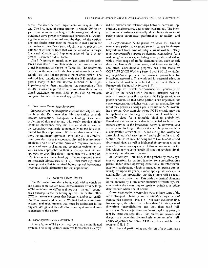
would use a densely interconnected backplane to couple the various IM functions together as shown in Fig. 6. Line cards, with fiber inputs for a number of customers, would be interconnected through the backplane to interline func- tion cards. These interline function cards would also con- nect to the feeder cards which contain the output fiber feeder lines. It is important to analyze the interconnection limits imposed by such a passive backplane structure.
Table I1 summarizes the circuit card requirements, based on the implementation discussed above, for both
BANWELL er al.: VERY LARGE ATM SWITCHING SYSTEMS 1231
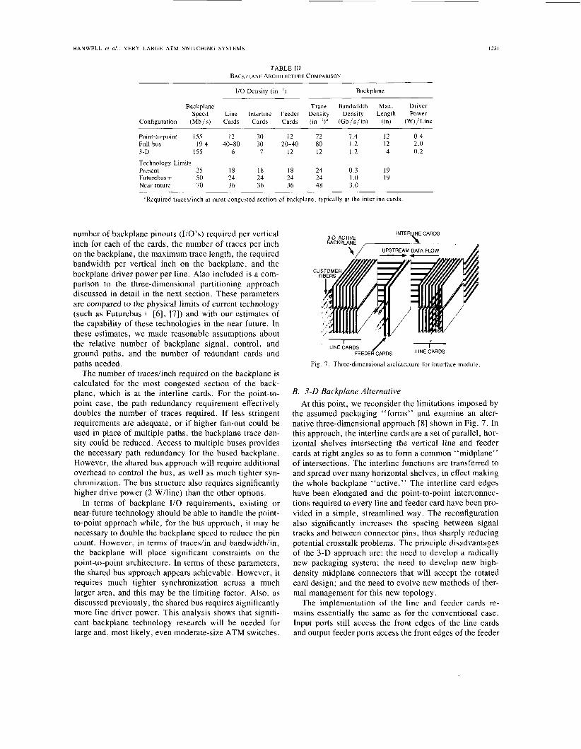
TABLE Ill BACKPLANE ARCHITECTURE COMPARISON
Backplane Speed
Configuration (Mb/s)
Point-to-point 155 Full bus 19.4 3-D 155
Technology Limits Present 25 Futurebusf 50 Near future 70
110 Density (in-’) Backplane
Trace Bandwidth Max. Driver Line Interline Feeder Density Density Length Power
Cards Cards Cards ( in- ’ )” (Gb/s/in) (in) (W)/Line
12 30 12 72 7.4 12 0.4 40-80 30 20-40 80 1.2 12 2.0
6 7 12 12 1.2 4 0.2
18 18 18 24 0 .3 19 24 24 24 24 1 .o 19 36 36 36 48 3.0
~ ~~~ ~
“Required tracesiinch at most congested section of backplane, typically at the interline cards
number of backplane pinouts (I/O’s) required per vertical inch for each of the cards, the number of traces per inch on the backplane, the maximum trace length, the required bandwidth per vertical inch on the backplane, and the backplane driver power per line. Also included is a com- parison to the three-dimensional partitioning approach discussed in detail in the next section. These parameters are compared to the physical limits of current technology (such as Futurebus+ [ 6 ] , [7]) and with our estimates of the capability of these technologies in the near future. In these estimates, we made reasonable assumptions about the relative number of backplane signal, control, and ground paths, and the number of redundant cards and paths needed.
The number of tracedinch required on the backplane is calculated for the most congested section of the back- plane, which is at the interline cards. For the point-to- point case, the path redundancy requirement effectively doubles the number of traces required. If less stringent requirements are adequate, or if higher fan-out could be used in place of multiple paths, the backplane trace den- sity could be reduced. Access to multiple buses provides the necessary path redundancy for the bused backplane. However, the shared bus approach will require additional overhead to control the bus, as well as much tighter syn- chronization. The bus structure also requires significantly higher drive power (2 W/line) than the other options.
In terms of backplane U0 requirements, existing or near-future technology should be able to handle the point- to-point approach while, for the bus approach, it may be necessary to double the backplane speed to reduce the pin count. However, in terms of tracedin and bandwidth/in, the backplane will place significant constraints on the point-to-point architecture. In terms of these parameters, the shared bus approach appears achievable. However, it requires much tighter synchronization across a much larger area, and this may be the limiting factor. Also, as discussed previously, the shared bus requires significantly more line driver power. This analysis shows that signifi- cant backplane technology research will be needed for large and, most likely, even moderate-size ATM switches.
INTERLINE CARDS I 3-D ACTIVE
BACKPLANE UPSTREAM DATA FLOW
C
I FEEDERCARDS LINE CARDS
Fig. 7. Three-dimensional architecture for interface module
B. 3 - 0 Backplane Alternative At this point, we reconsider the limitations imposed by
the assumed packaging “forms” and examine an alter- native three-dimensional approach [8] shown in Fig. 7. In this approach, the interline cards are a set of parallel, hor- izontal shelves intersecting the vertical line and feeder cards at right angles so as to form a common “midplane” of intersections. The interline functions are transferred to and spread over many horizontal shelves, in effect making the whole backplane “active. ” The interline card edges have been elongated and the point-to-point interconnec- tions required to every line and feeder card have been pro- vided in a simple, streamlined way. The reconfiguration also significantly increases the spacing between signal tracks and between connector pins, thus sharply reducing potential crosstalk problems. The principle disadvantages of the 3-D approach are: the need to develop a radically new packaging system; the need to develop new high- density midplane connectors that will accept the rotated card design; and the need to evolve new methods of ther- mal management for this new topology.
The implementation of the line and feeder cards re- mains essentially the same as for the conventional case. Input ports still access the front edges of the line cards and output feeder ports access the front edges of the feeder
1232 IEEE JOURNAL ON SELECTED AREAS IN COMMUNICATIONS. VOL. 9, NO. 8. OCTOBER 1991
cards. The interline card implementation is quite differ- ent. The first stage of concentration is rotated 90” to or- ganize and minimize the length of the wiring and, thereby, minimize drive power for interstage connections. Assum- ing the same enclosure volume, the depth of the vertical line and feeder cards must be reduced to make room for the horizontal interline cards, which, in turn, reduces the number of customer lines that can be served on a single line card. Circuit card implementation of the 3-D ap- proach is summarized in Table 11.
The 3-D approach greatly alleviates some of the prob- lems encountered in implementations that use a conven- tional backplane, as shown in Table 111. The bandwidth per inch is the same as for the bus architecture but signif- icantly less than for the point-to-point architecture. The reduced lead lengths possible with the 3-D architecture permit many of the I/O interconnections to be high- impedance rather than transmission-line connections. This results in lower required drive power than the conven- tional backplane options. EM1 might also be reduced compared to the conventional approaches.
C. Backplane Technology Summagi Our analysis of the backplane interconnectivity require-
ments in the IM shows that this application severely stresses conventional backplane technology. Continued evolution of this technology will surely provide higher levels of interconnectivity, but it is not at all certain that the technology can scale economically to the levels re- quired for this application. We have also shown that a more revolutionary approach, involving a 3-D architec- ture, provides richer interconnectivity and is more power efficient. The 3-D structure, however, requires the devel- opment of new packaging and connector technology, as well as new approaches to thermal management. A third approach to providing richer interconnectivity , using op- tical interconnection technology, is being explored in sev- eral research laboratories [9]-[ 121. Even more significant development effort is required before optical backplanes become a viable alternative for this application.
IV. SYSTEM-LEVEL ISSUES The IM model provides a framework within which we
can assess some system-level consequences of very large ATM switches. At different times our “system” bound- aries encompass the switching system, the central office (CO) or remote enclosure that houses it, and occasionally the entire broadband network. We first look at some basic system-level requirements that must be addressed in the physical design and then develop some system-level con- sequences of the design.
A . Basic System-Level Parameters A very large ATM switch will be a very complicated
system. The complications manifest themselves as a myr-
iad of tradeoffs and relationships between hardware, op- erations, maintenance, and control constraints. The inter- actions and constraints generally affect three categories of basic system parameters: performance, reliability, and cost.
1) Performance: ATM packet switches will have to meet many performance requirements that are fundamen- tally different from those of today’s circuit switches. They must economically support on-demand connections for a wide range of services, including voice, data, and video, with a wide range of traffic characteristics, such as call duration, bandwidth, burstiness, and tolerance to delay and error. Considerable progress has been made by CCITT SG XVIII Working Party 6 and T l Q l . 3 on defin- ing appropriate primary performance parameters for broadband networks. This work and its potential effect on a broadband switch is reflected in a recent Bellcore Framework Technical Advisory [ 131.
The required switch performance will generally be driven by the service with the most stringent require- ments. In some cases this service is POTS (plain old tele- phone service), so that some performance objectives for current-generation switches (e.g., system availability cri- teria) may persist as design goals for future ATM switch- ing systems. One example where POTS criteria may not be applicable is blocking. Current circuit switches are normally sized for a tolerable blocking probability. Broadcast entertainment video is expected to be an im- portant service in the broadband network, however, and virtually no blocking of this service will be permissible in a competitive environment. Since sizing the switch for zero blocking of all services will probably not be cost ef- fective, the switch must be designed to handle nonblocked distributed video as well as high availability point-to-point services. Some consequences of this requirement on the IM, which may have to handle all types of services simul- taneously, are discussed below.
2) Reliability: Reliability is the probability that a sys- tem will perform its required function for a prescribed time period under stated operating conditions. In telecommu- nications equipment, which is intended to operate contin- uously for up to 40 years, a more appropriate measure is availability, the probability that the system will be ready for use at any given time. This adds the critical elements of maintainability to the other elements of reliability, en- compassing the mean time to repair or switch to a redun- dant module when a fault occurs.
Current-generation electronic switches have some of the most stringent reliability and availability objectives of commercial systems [14], [15]. For each customer line, for example, the objective is less than 28 min/year of downtime (unavailability) and less than 0.13 fail- ures/year. Since objectives are determined to a great ex- tent by technical feasibility-and electronic devices and designs are becoming increasingly more reliable-reli- ability objectives for future ATM switches could be even tougher [16], [17].
The physical partitioning and design of a system has a
BANWELL et al.: VERY LARGE ATM SWITCHING SYSTEMS 1233
direct relation to its availability. Consider, for example, the IM line cards. A first-order reliability analysis shows that line availability could be almost doubled by provid- ing one redundant (or ‘‘protection” ) line-circuit for every eight customers, i.e., one per line card in our model IM[ 181. Even one redundant line-circuit per 500 lines (one per IM) could substantially increase availability [ 161. A second factor that determines line availability is the num- ber of lines that are terminated on each card. The eight lines per card assumed for the 3-D configuration was a compromise between the probability of card unavailabil- ity from per-line component failures and the probability of blocking because of an inadequate number of intercon- nection paths to the interline cards. From an operational standpoint, a number of considerations could lead to a reduction of this number; these considerations have had a strong influence on the design of commercial line cards [19]. Such reductions would alter some partitioning as- sumptions and change the proposed physical implemen- tation. However, we do not believe that they would rad- ically alter the physical design consequences from this analysis.
The human factors design of the switch is also critical to system availability. In current-generation switches, a large fraction (almost 42%) of downtime is caused by pro- cedural (human) errors [20]. This suggests that the avail- ability of future ATM switches will be significantly af- fected by their maintainability, including such factors as accessibility for inspection, repair and upgrade, simple fault location and testing procedures, and protection of functional elements during repair. In the potentially multivendor environment of an ATM switch, standard- ization of the human interfaces will also be an important factor.
Cost: The third basic system parameter is cost, which includes not only the first EF&I (engineered, furnished, and installed) cost, but also the lifetime operating cost of the system. The EF&I cost is directly related to the per- formance and reliability that is built into the system. For example, the 1 : 8 line redundancy discussed above dou- bles line availability but increases the initial cost of the line cards by at least 1/8. Further, the MCM packaging technologies discussed in Section I1 will probably be more expensive initially but can provide greater packaging den- sities (and thus higher speeds) and better system avail- ability because their modularity simplifies maintenance and repair.
In addition to the EF&I first cost of the system, the physical design affects other cost factors of the system. One of the most significant of these is energy cost. We show in the next section that the power requirements of very large ATM switches could be substantially larger than those of today’s digital switches. One metric for quantifying the cost impact of power is the capital worth of a watt (CWOW) [21], [22]. The CWOW is the present worth of all costs associated with providing one watt of power continuously over a system’s lifetime; it includes both the direct energy cost of the watt and the capital and
energy costs of all the equipment necessary to supply the watt. (For example, the capital costs include the batteries, air-conditioning, and power-processing equipment in the central office.) Assuming a 30-year system lifetime, a lOC/kW * h energy cost, a 4 % energy inflation rate, a 12% cost of capital, and a 34% federal income tax, the CWOW at the output of a CO battery plant is $19.48 per watt.
B. System-Level Consequences of the IM Model Three major system-level issues were identified during
the IM model design and are discussed below. The first is its substantial power consumption, which could have a critical impact on the total system reliability, perfor- mance, and cost. The second issue relates to protocol and software constraints on optimization of the IM, which cannot be divorced from its physical design. Finally, there are several power-efficient broadcast service delivery op- tions which may not readily integrate into the digital en- vironment of the IM.
I) Power: Power consumption affects all three of the basic system parameters. Power-induced temperature variations can affect both information delay and transfer accuracy. Interruption in power delivery is a major cause of system unavailability, while power-induced tempera- ture gradations and variations reduce component and module reliability. Finally, the costs of purchasing and conditioning power and removing the waste heat contrib- ute significantly to the lifecycle cost of the switch.
The impact of power on very large ATM switches can be estimated from the power requirements of the IM model. These requirements are summarized in Table IV for the different IM subsystems under three traffic condi- tions. The first traffic condition (0% utilization) defines the minimum power usage of the IM. For this condition, when there is little activity on the switch, only those cir- cuits required to maintain SONET conformance at the in- terfaces are active; these circuits include the 155 Mb/s and 2.4 Gb/s framing and optoelectronic functions and some clock and control circuits. The second traffic con- dition (full capacity) is an estimate of the normal busy hour usage; for this condition, only 10% of the customers lines are effectively utilized and the IM power consump- tion is about 2500 W. The final traffic condition assumes an IM architecture that supports digital advanced televi- sion (ATV) distribution on a dedicated interline card. We assume that two additional downstream interline cards and one additional feeder card will be required to provide this service and that it would consume an additional 1500 W per IM over the full-capacity condition.
The extrapolation of the IM power requirements to an IM equipment frame and a 64 000-line CO are also shown in Table IV. As a comparison, consider a typical current- generation digital switch [23], which has several types of interface units. The two extremes of these interface units are the line and digital-trunk modules. A line module can typically terminate about 600 analog lines, requires ap-
1234 IEEE JOURNAL ON SELECTED AREAS I N COMMUNICATIONS, VOL. 9. NO. 8. OCTOBER 1991
TABLE IV POWER ESTIMATES FOR MODEL 1M
0% Full Digital Utilization Capacity ATV
Per subscriber power (W) Board power (W)
Line card Upstream interline card Downstream interline card Feeder card”
IM power (W) Frame power (W) CO power (kW) Frame power density (W /ft2)
1.2
8 I 2
18 620
1200 80
115
5
16 26 36
I80 2500 5000
305 450
8
36 26 36
4000 8000 500 140
I no
Each feeder card includes one stage of the upstream and downstream interline functions.
proximately half a frame of space, and dissipates about 800 W at an 8 CCS traffic load (equivalent to about 9 Mb/s throughput or approximately 22 % utilization). A digital trunk module, on the other hand, may terminate up to 20 T1 trunks (about 31 Mb/s throughput), requires one equipment frame, and dissipates about 1000 W. Since one SONET OC-3 line of the IM carries almost 17 times the traffic of a line module and 5 times that of a trunk module yet dissipates less than 8 W, the model IM would clearly be very power efficient on a “per-bit’’ basis.
On a per-office basis, however, the power requirement of the ATM switching system could be significantly larger than that of current switches. If we assume that the ratio of IM to total switch power will be similar to that of the current-generation switch (about 4 to 7), the total power requirement for the ATM switch may be between 0.5 and 0.9 MW-depending on the penetration of digital ATV. Since current-generation switches with the same number of lines consume less than 100 kW, it is evident that power will be a critical issue in the design of large ATM switches.
Some of the effects of this potential power increase on the switch, the CO, and the network of the future include the following.
Thermal Management: New technologies will be needed to manage the potential tenfold increase in power dissipation. (Chip temperatures over 300°C could result if natural-air-convection cooling, the major cooling tech- nique used in U.S. central offices today, were used in the IM model.) These techniques will alter the philosophy and strategies of central office and remote environmental con- trol.
Space: The additional space required for providing, conditioning, and removing the extra power will be a con- cern, particularly in remote sites, where 4-8 times the space required to provide normal IM functions may be required to provide battery backup.
Reliability: Hardware reliability depends both on the absolute temperature and on temperature stability. Trade- offs between the development of sturdier hardware, better thermal management schemes,and reductions and/or real- location of availability may be required.
Cost: The 30-year lifecycle cost of purchasing, con- ditioning, and dissipating this power (and the cost of the space to house these functions) could be between 10 and 17 million dollars (using the $19.48 CWOW).
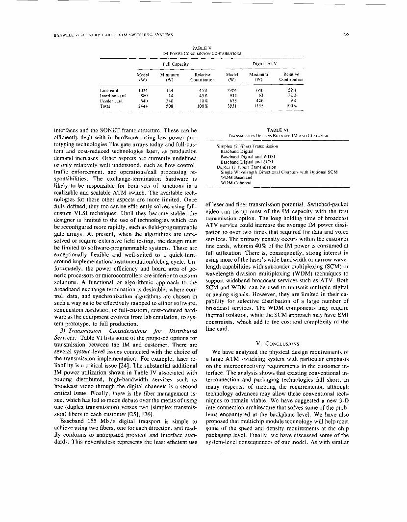
2) System Optimization Considerations: The IM power consumption given in Table IV can be divided into two main categories: the power required by the gates, etc., through which a cell actually passes (intrinsic routing) and that required to configure the gates for call processing functions (control and OA&M). The first category defines the minimum power required to get data into and out of the IM and to transfer it from input to output via fixed paths. The model used to calculate the demands for in- trinsic routing is described in the Appendix, and includes the power expended in moving data through the optoelec- tronic interfaces, the SONET/ATM-cell assembly/disas- sembly process, and a fixed path within the interline cards. This minimum routing power is compared in Table V with the estimated IM model power consumption for the full- capacity and digital ATV conditions. The relative contri- bution of each function to the net difference is also re- ported. For example, the relative contribution of the line cards at full capacity is (1024 - 154)/(2444 - 508) = 0.45.
The feeder cards perform minor cell routing functions, as reflected by the small 9-10% contribution to the dif- ference. Most of the interline card power dissipation re- sults from cell buffering and the control of ATM-cell rout- ing; however, their overall contribution reflects the me- dium size of these boards. The primary penalty for route diversity on the interline card will be associated with soft- ware control, rather than power dissipation. The numer- ous line cards dissipate most of the power associated with cell processing, especially when broadcast services are distributed digitally. Much of the power dissipation of the switch is not intrinsic and can be attributed to accommo- dating uncertainty in the system. Each operation per- formed to accommodate uncertainty, such as cell buffer- ing or route selection, costs energy. Table V shows that this accounts for 71-79% of the total power expended by the IM, and consequentially there is substantial opportu- nity for optimization.
There are additional penalties for other uncertainties. The power costs and limitations examined in this study are associated primarily with hardware and reflect, there- fore, anticipated evolutions in electronics and packaging technologies. The IM will not be built using conventional routing architectures and technology, however-power requirements, for one thing, would not be acceptable. Significant optimization must occur. This optimization also extends to the software required to manage the basic operation of the IM, including functions such as call set- up and tear-down, resource allocation, performance mon- itoring, special function implementation, and billing. The complexity of the software to manage the IM will increase with the degree of route diversity provided.
Many aspects of the broadband exchange termination are well defined, such as the use of OC-3 or OC-12 optical
BANWELL er al.. VERY LARGE ATM SWITCHING SYSTEMS 1235
TABLE V IM POWER CONSUMPTION CONTRIBUTIONS
Full Capacity Digital ATV
Model Minimum Relative Model Minimum Relative Contribution (W) (W) Contribution (W) (W)
Line card 1024 154 45 % 2304 646 59 % Interline card 880 14 45 % 952 63 32 ’% Feeder card 540 340 10% 615 426 9% Total 2444 508 100% 393 1 1 I35 100%
interfaces and the SONET frame structure. These can be efficiently dealt with in hardware, using low-power pro- totyping technologies like gate arrays today and full-cus- tom and cost-reduced technologies later, as production demand increases. Other aspects are currently undefined or only relatively well understood, such as flow control, traffic enforcement, and operations/call processing re- sponsibilities. The exchange-termination hardware is likely to be responsible for both sets of functions in a realizable and scalable ATM switch. The available tech- nologies for these other aspects are more limited. Once fully defined, they too can be efficiently solved using full- custom VLSI techniques. Until they become stable, the designer is limited to the use of technologies which can be reconfigured more rapidly, such as field-programmable gate arrays. At present, when the algorithms are unre- solved or require extensive field testing, the design must be limited to software-programmable systems. These are exceptionally flexible and well-suited to a quick-turn- around implementation/instrmentation/debug cycle. Un- fortunately, the power efficiency and board area of ge- neric processors or microcontrollers are inferior to custom solutions. A functional or algorithmic approach to the broadband exchange termination is desirable, where con- trol, data, and synchronization algorithms are chosen in such a way as to be effectively mapped to either software, semicustom hardware, or full-custom, cost-reduced hard- ware as the equipment evolves from lab emulation, to sys- tem prototype, to full production.
3) Transmission Considerations for Distributed Services: Table VI lists some of the proposed options for transmission between the IM and customer. There are several system-level issues connected with the choice of the transmission implementation. For example, laser re- liability is a critical issue [24]. The substantial additional IM power utilization shown in Table IV associated with routing distributed, high-bandwidth services such as broadcast video through the digital channels is a second critical issue. Finally, there is the fiber management is- sue, which has led to much debate over the merits of using one (duplex transmission) versus two (simplex transmis- sion) fibers to each customer [25], [26].
Baseband 155 Mb/s digital transport is simple to achieve using two fibers, one for each direction, and read- ily conforms to anticipated protocol and interface stan- dards. This nevertheless represents the least efficient use
TABLE VI TRANSMISSION OPTIONS BETWEEN 1M A N D CUSTOMER
Simplex (2 Fiber) Transmission Baseband Digital Baseband Digital and WDM Baseband Digital and SCM
Duplex (1 Fiber) Transmission Single Wavelength Directional Couplers with Optional SCM WDM Baseband WDM Coherent
of laser and fiber transmission potential. Switched-packet video can tie up most of the IM capacity with the first transmission option. The long holding time of broadcast ATV service could increase the average IM power dissi- pation to over two times that required for data and voice services. The primary penalty occurs within the customer line cards, wherein 40% of the IM power is consumed at full utilization. There is, consequently, strong interest in using more of the laser’s wide bandwidth or narrow wave- length capabilities with subcarrier multiplexing (SCM) or wavelength division multiplexing (WDM) techniques to support wideband broadcast services such as ATV. Both SCM and WDM can be used to transmit multiple digital or analog signals. However, they are limited in their ca- pability for selective distribution of a large number of broadcast services. The WDM components may require thermal isolation, while the SCM approach may have EM1 constraints, which add to the cost and complexity of the line card.
V. CONCLUSIONS We have analyzed the physical design requirements of
a large ATM switching system with particular emphasis on the interconnectivity requirements in the customer in- terface. The analysis shows that existing conventional in- terconnection and packaging technologies fall short, in many respects, of meeting the requirements, although technology advances may allow these conventional tech- niques to remain viable. We have suggested a new 3-D interconnection architecture that solves some of the prob- lems encountered at the backplane level. We have also proposed that multichip module technology will help meet some of the speed and density requirements at the chip packaging level. Finally, we have discussed some of the system-level consequences of our model. As with similar
1236 IEEE JOURNAL ON SELECTED AREAS IN COMMUNICATIONS. VOL. 9. NO. 8. OCTOBER 1991
UPSTREAM Receiver Framer Formatter SONET MUX
0.5W 0.3W 0.5W I-50cm-I 2.66W
Transmitter Framer Formatter 0.3W 0.3W 0.5W
SONET Demux 2.66W Interline
DOWNSTREAM
(a)
Pad Gates $Er Pad
PPi% 2.0 pF + 2.5pF + 1.7pF t 2.OpF = 8.2pF
Interline Chip Model
(b) Fig. 8. Intrinsic routing power model
large, complex systems, physical design will play a key role in determining the feasibility of terabit/second- throughput ATM switching systems.
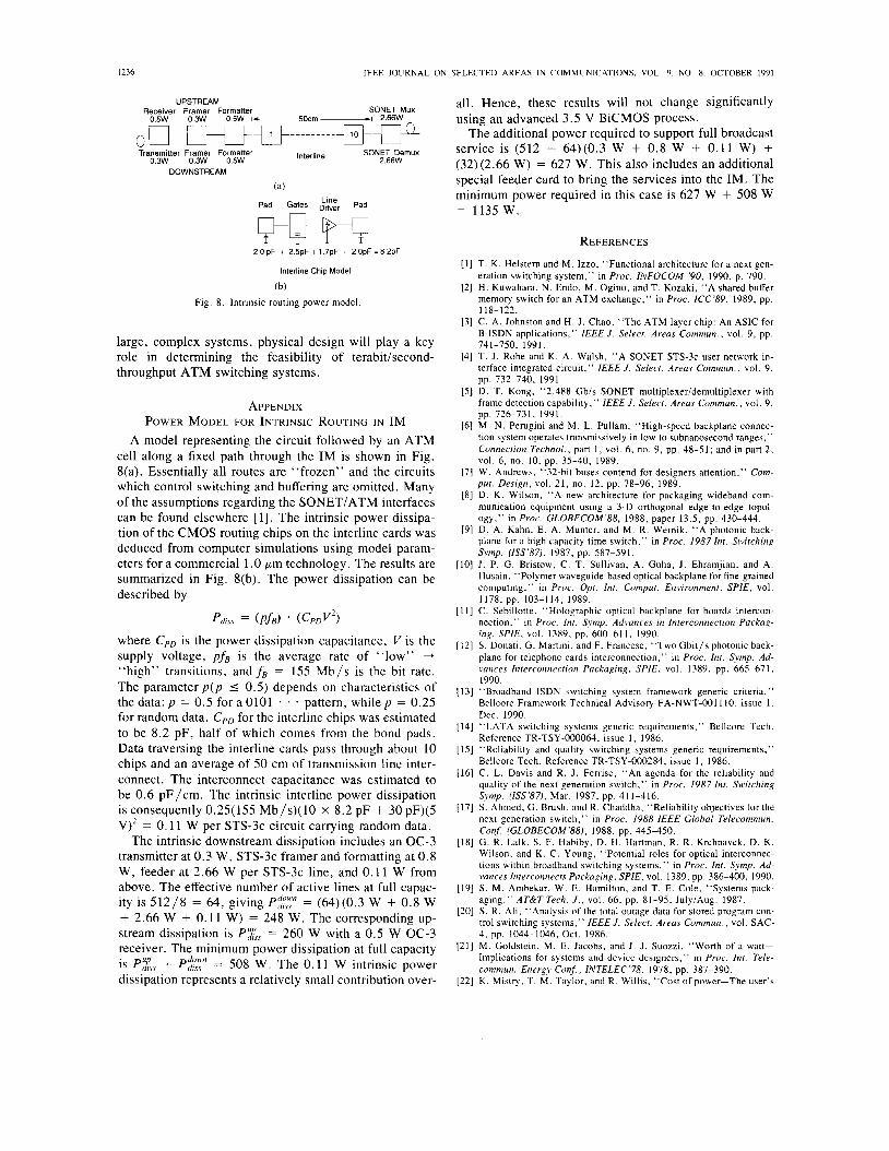
APPENDIX POWER MODEL FOR INTRINSIC ROUTING I N IM
A model representing the circuit followed by an ATM cell along a fixed path through the IM is shown in Fig. 8(a). Essentially all routes are “frozen” and the circuits which control switching and buffering are omitted. Many of the assumptions regarding the SONETIATM interfaces can be found elsewhere [ l ] . The intrinsic power dissipa- tion of the CMOS routing chips on the interline cards was deduced from computer simulations using model param- eters for a commercial 1 .O pm technology. The results are summarized in Fig. 8(b). The power dissipation can be described by
p d u , = ( P f B ) ( c P D v 2 )
where C,, is the power dissipation capacitance, I/ is the supply voltage, pfB is the average rate of “low” +
“high” transitions, andfB = 155 Mb/s is the bit rate. The parameter p ( p I 0.5) depends on characteristics of the data: p = 0.5 for a 0101 * * * pattern, while p = 0.25 for random data. C,, for the interline chips was estimated to be 8.2 pF, half of which comes from the bond pads. Data traversing the interline cards pass through about 10 chips and an average of 50 cm of transmission line inter- connect. The interconnect capacitance was estimated to be 0.6 pF/cm. The intrinsic interline power dissipation is consequently 0.25(155 Mb/s)( 10 x 8.2 pF + 30 pF)(5 V)2 = 0.11 W per STS-3c circuit carrying random data.
The intrinsic downstream dissipation includes an OC-3 transmitter at 0 .3 W, STS-3c framer and formatting at 0.8 W, feeder at 2.66 W per STS-3c line, and 0.11 W from above. The effective number of active lines at full capac- ity is 512/8 = 64, giving Pi::“ = (64)(0.3 W + 0.8 W + 2.66 W + 0.11 W) = 248 W. The corresponding up- stream dissipation is P X , = 260 W with a 0.5 W OC-3 receiver. The minimum power dissipation at full capacity is Ps:,, + Pi:“ = 508 W. The 0.11 W intrinsic power dissipation represents a relatively small contribution over-
all. Hence, these results will not change significantly using an advanced 3.5 V BiCMOS process.
The additional power required to support full broadcast service is (512 - 64)(0.3 W + 0.8 W + 0.11 W) + (32)(2.66 W) = 627 W. This also includes an additional special feeder card to bring the services into the IM. The minimum power required in this case is 627 W + 508 W = 1135 W.
REFERENCES
[I ] T. K. Helstern and M. Izzo, “Functional architecture for a next gen- eration switching system,” in Proc. INFOCOM ’90, 1990, p. 790.
121 H. Kuwahara, N. Endo, M. Ogino, and T. Kozaki, “A shared buffer memory switch for an ATM exchange,” in Proc. ICC’89, 1989, pp.
[3] C. A. Johnston and H. J . Chao, “The ATM layer chip: An ASIC for B-ISDN applications,” IEEE J . Select. Areas Commun., vol. 9, pp. 741-750, 1991.
[4] T . J . Robe and K. A. Walsh, “A SONET STS-3c user network in- terface integrated circuit,” IEEE J . Select. Areas Commun., vol. 9 ,
[5] D. T. Kong, “2.488 Gbis SONET multiplexeridemultiplexer with frame detection capability,” IEEE J . Select. Areas Commun., vol. 9 , pp. 726-731, 1991.
[6] M. N. Perugini and M. L. Pullam, “High-speed backplane connec- tion system operates transmissively in low to subnanosecond ranges,” Connection Technol., part I , vol. 6, no. 9 , pp. 48-51; and in part 2, vol. 6, no. IO, pp. 35-40, 1989.
[71 W. Andrews, “32-bit buses contend for designers attention,” Com- pur. Design, vol. 21, no. 12, pp, 78-96, 1989.
[SI D. K. Wilson, “A new architecture for packaging wideband com- munication equipment using a 3-D orthogonal edge-to-edge topol- ogy,” in Proc. GLOBECOM’88, 1988, paper 13.5, pp. 430-444.
[9] D. A. Kahn, E. A. Munter, and M. R. Wernik, “A photonic back- plane for a high capacity time switch,” in Proc. 1987Inr. Swirching Symp. (ISS’87). 1987, pp. 587-591.
IO] J . P. G. Bristow, C. T . Sullivan, A. Guha. J . Ehramjian, and A. Husain, “Polymer waveguide-based optical backplane for fine-grained computing,” in Proc. Opt. Int. Comput. Environment, SPIE, vol.
I11 C. Sebillotte, “Holographic optical backplane for boards intercon- nection,” in Proc. Int. Synp. Advances in Inrerconnection Packag- ing, SPIE, vol. 1389, pp. 600-611, 1990.
121 S . Donati, G. Martini, and F. Francese. “Two Gbit/s photonic back- plane for telephone cards interconnection,” in Proc. Int. Symp. Ad- vances Interconnection Packaging, SPIE, vol. 1389, pp. 665-671, 1990.
[ 131 “Broadband ISDN switching system framework generic criteria,” Bellcore Framework Technical Advisory FA-NWT-0011 I O . issue 1 , Dec. 1990.
[ 141 “LATA switching systems generic requirements,” Bellcore Tech. Reference TR-TSY-000064. issue 1 , 1986.
[ 151 “Reliability and quality switching systems generic requirements.” Bellcore Tech. Reference TR-TSY-000284, issue I , 1986.
[16] C. L. Davis and R. J . Ferrise, “An agenda for the reliability and quality of the next generation switch,” in Proc. 1987Int. Switching Symp. (ISS’87) , Mar. 1987, pp. 411-416.
[17] S. Ahmed, G. Brush. and R. Chaddha, “Reliability objectives for the next generation switch,” in Proc. 1988 IEEE Global Telecommun. Con6 (GLOBECOM’88), 1988, pp. 445-450.
[I81 G. R. Lalk, S . F. Habiby, D. H. Hartman, R. R. Krchnavek, D. K. Wilson, and K. C. Young, “Potential roles for optical interconnec- tions within broadband switching systems,” in Proc. Int. Symp. Ad- vances Interconnects Packaging, SPIE, vol. 1389, pp. 386-400, 1990.
[19] S . M. Ambekar, W. E. Hamilton, and T. E. Cole, “Systems pack- aging,” AT&T Tech. J . , vol. 66, pp. 81-95, July/Aug. 1987.
[20] S. R. Ali, “Analysis of the total outage data for stored program con- trol switching systems,’’ IEEE J . Selecr. Areas Commun., vol. SAC-
[21] M. Goldstein, M. E. Jacobs, and J . J . Suozzi, “Worth of a watt- Implications for systems and device designers,” in Proc. Int. Tele- commun. Energy Conf , INTELEC’78, 1978, pp. 387-390.
[22] K. Mistry. T . M. Taylor, and R. Willis, “Cost of power-The user’s
118-122.
pp. 732-740, I99 I .
1178, pp. 103-1 14, 1989.
4, pp. 1044-1046, Oct. 1986.
BANWELL er al.: VERY LARGE ATM SWITCHING SYSTEMS 1237
perspective.” in Proc. Fiber Subscriber Loop ConForum ‘89. 1989, pp. D5.9-D5.14., also in Fiber Inr. Oprics. vol. 9 , issue 3, 1991.
[23] “DMS-100 family of digital switches,” Northern Telecom Telesis, Special Issue, vol. 4, 1980.
1241 M. Fukuda, “Laser and LED reliability update,” J . LightwuL3e Tech- nol.. vol. 6 , pp. 1488-1495, 1988.
[25] L. J . Baskerville, “Two fibers or one?,” J . Lightwave Technol., vol.
[26] “Generic requirements and objectives for fiber in the loop systems,” Bellcore Tech. Advisory TA-NWT-000909. issue 1 , Dec. 1990.
7, pp. 1733-1740, 1989.
He has authored or C I
patents.
Thomas C. Banwell (M’90) received the M.S. degree in electrical engineering and the Ph.D. de- gree in applied physics from the California Insti- tute of Technology, Pasedena. in 1980 and 1986, respectively. His thesis work was on atomic trans- port.
Since 1986 he has been a Member of the Tech- nical Staff at Bellcore, Morristown. NJ. He is en- gaged in the study of performance limitations in low-powerihigh-speed circuits for fiber-optic tele- communications and data processing applications.
muthored :nore than 20 technical papers and has two
Renee C. Estes received the B S M E. and M S M.E degrees from New Mexico State Uni- versity, La\ Cruces, and the Ph D degree in me- chanical engineering from Columbia University, New York, NY
She has worked in the areas of thermal control and energy systems at Bell Laboratories. Singer Corporate Research and Development Labs. and Lockheed Electronics Company Since 1984 she has been with Bellcore, Morristown, NJ. where she is currently a Member of Technical Staff in
the Energy Systems Technology Research Group.
Sarry F. Habiby (M’88) received the B S degree from Oklahoma State University, Stillwater. i n
1980, and the M S and Ph D degrees from The Ohio State University. Columbus. in 1982 and 1986, respectively, all in electrical engineering
He was a Research Assistdnt in opticdl com- puting at the Electro Science Laboratory, Ohio State University, from 1980 to 1986 In 1986 he joined Bellcore, Red Bank, NJ. and has contrib- uted in the fields of optical interconnects, optical facility and protection switching, video transmis-
sion systems, next generation switch functional architectures, and broad- band switch physical design He is currently working on optical intercon- nect applications using programmable 2-D source and modulator arrays
Dr Habiby is a member of the Optical Society of America
Gary A. Hayward was born in Whittier. CA, in 1953. He received the B.S. degree in physics from the California Institute of Technology, Pasedena. in 1975. and the Ph.D. degree in applied physics from Stanford University, Stanford. CA, in 1980.
From 1980 to 1984 he worked at TRW on sev- eral high-speed optical communications and pro- cessing systems, and in 1984 he joined Bellcore, Red Bank, NJ. to take part in their broadband switching research. He is currently District Man- - ager of the Broadband Connection Management Group.
Thomas K. Helstern received the B S M E de- gree from The Cooper Union, New York, NY, in
1982. and the M S degree in operations research from Columbia University. New York, NY. in 1984
In 1982 he joined Bell Laboratories where he worked on network switching economics. In 1984 he moved to Bellcore, Red Bank, NJ. where he has worked on various aspects of broadband switching including video teleconferencing. Bell- core‘\ Next Generation Switch project. and
broadband ISDN standards. He is currently working on generic require- ments for broadband switching systems
Gail R . Lalk (S’84-S‘85-M’85-M’86-M‘87) re- ceived the B.S. and M.S. degrees in electrical en- gineering from Washington University, St. Louis, MO, in 1986 aqd 1987. respectively.
In 1987 she joined the Interconnection Tech- nology Research District at Bellcore. Morristown, NJ. Her main topic of research has been the in- vestigation of the feasibility of board-level optical interconnections in high-speed systems. Her present research interests lie in identifying appli- . . .
cations for optical interconnections in telecom- munications switching systems.
Ms. Lalk is a member of Sigma Xi and Tau Beta Pi. She is the 1990- 1991 Vice-Chair of the IEEE Communications Society Technical Com- mittee on Interconnections within High-speed Digital Systems.
core. Red Bank. NJ. opment pertaining t electronics.
\1
0
Derek D. Mahoney received the B.S. degree in mechanical engineering from Howard University, Washington, DC. and the S.M. degree in aero- nautics and astronautics from the Massachusetts Institute of Technology, Cambridge, in 1978 and 1980, respectively.
From 1980 lo 1983 he worked for the Bell Tele- phone Laboratories, Inc., North Andover, MA, where he was mainly concerned with the thermal management of microelectronic components, sub- systems. and systems. In 1984, he joined Bell-
ihere he has been involved in research and devel- the interconnect and packaging of high-speed
Donald K. Wilson (M’64-M’79) received the B.S. and M.S. degrees in physics from the Penn- sylvania State University. University Park. in 1950 and 1951, respectively, and the Ph.D. de- gree in physics from Rutgers University, New Brunswick. NJ. in 1963.
He was with AT&T Bell Laboratories from 1951 to 1981, where he worked in the areas of semi- conductor device development, fundamental properties of semiconductor materials. radiation effects on materials and devices. and analysis of
interconnection networks in telecommunications systems. Since joining Bellcore. Morristown, NJ. in 1984. he has been developing packaging and interconnection concepts and designs for high-speed telecommunications systems. He has also been continuing his long-term effort in characterizing and developing a generic discipline for the roles of physical interconnec- tions across the whole range of telecommunications equipment and net- works.
Dr. Wilson is a member of Phi Beta Kappa and Sigma Xi. He has been active for many years in a number of profesaional activities with the IEEE, APS, and with local professional sounding board networks. His work with these groups has spanned the range from technical to career-centered.
IEEE JOURNAL ON SELECTED AREAS IN COMMUNICATIONS. VOL. 9. NO. 8, OCTOBER 1991 1238
Kenneth C. Young, Jr. (M’87-SM’89) received the B S degree (cum laude) from St. Joseph’s College, Philadelphia, PA, in 1972 and the M S and Ph.D. degrees in 1973 and 1978 from the University of Pennsylvania, Philadelphia, all in
physics. From 1978 through 1983 he was a Member of
the Technical Staff at Bell Telephone Laborato- ries, Whippany, NJ, involved in systems engi- neering projects for central office cross-connects and digital loop carrier systems From 1980
through 1983 he was also an Adjunct Assistant Professor of Physics at the County College of Moms. Since I984 he has been District Manager of the
Interconnection and Access Technology Research Group at Bellcore. Mor- ristown, NJ His group is responsible for research into high-speed electrical and optical interconnections, OEIC design for optical interconnect and telecommunications applications, SONET/ATM subsystem prototypes, and novel packaging approaches for high-speed electrical and optoelectronic circuits. He has also lead team studies of physical design altemat~ves for large-capacity broadband switches He has more than 20 research publi- cations
Dr. Young is a member of the American Physical Society, Sigma Pi Sigma, and the Optical Society of America