Moldova - Digitally signed by Cojocaru Vladimir Date - MTender
Upload
khangminh22Category
view
1download
0
SBOS289A − NOVEMBER 2003 − REVISED DECEMBER 2003
Digitally Controlled Microphone Preamplifier
PGA2500
FEATURES Fully Differential Input-to-Output Architecture Digitally Controlled Gain Using Serial Port
Interface:− Gain Range: 10dB through 65dB, 1dB per
step− Unity (0dB) Gain Setting via Serial Port or
Dedicated Control Pin Dynamic Performance:
− Equivalent Input Noise with Z S = 150Ω andGain = 30dB: −128dBu
− Total Harmonic Distortion plus Noise(THD+N) with Gain = 30dB: 0.0004%
Zero Crossing Detection Minimizes AudibleArtifacts when Gain Switching
Integrated DC Servo Minimizes Output OffsetVoltage
Common-Mode Servo Improves CMRR Four-Wire Serial Control Port Interface:
− Simple Interface to Microprocessor orDSP Serial Ports
− Supports Daisy-Chaining of MultiplePGA2500 Devices
Dedicated Input Pin for Selecting Unity Gain Overload Output Pin Provides Clipping
Indication Four General-Purpose Digital Output Pins Requires ±5V Power Supplies Available in an SSOP-28 Package
APPLICATIONS Microphone Preamplifiers and Mixers
Digital Mixers and Recorders
DESCRIPTIONThe PGA2500 is a digitally controlled, analog microphonepreamplifier designed for use as a front end for high-performance audio analog-to-digital converters (ADCs). ThePGA2500 features include low noise, wide dynamic range,and a differential signal path. An on-chip DC servo loop isemployed to minimize DC offset, while a common-modeservo function may be used to enhance common-moderejection.
The PGA2500 features a gain range of 10dB through 65dB(1dB/step), along with a unity gain setting. The wide gainrange allows the PGA2500 to be used with a variety ofmicrophones. Gain settings and internal functions areprogrammed using a 16-bit control word, which is loadedusing a simple serial port interface. A serial data output pinprovides support for daisy-chained connection of multiplePGA2500 devices. Four programmable digital outputs areprovided for controlling the external switching of input pads,phantom power, high pass filters, and polarity reversalfunctions. The PGA2500 requires both +5V and −5V powersupplies and is available in a small SSOP-28 package.
All trademarks are the property of their respective owners.
! !
www.ti.com
Copyright 2003, Texas Instruments Incorporated
Please be aware that an important notice concerning availability, standard warranty, and use in critical applications of Texas Instrumentssemiconductor products and disclaimers thereto appears at the end of this data sheet.

"#$%%
SBOS289A − NOVEMBER 2003 − REVISED DECEMBER 2003
www.ti.com
2
ABSOLUTE MAXIMUM RATINGSOver operating free-air temperature range unless otherwise noted(1)
PGA2500 UNIT
Supply Voltage, VA+ +5.5 V
Supply Voltage, VA− −5.5 V
Supply Voltage, VD− −5.5 V
Voltage Difference, VA− to VD− Less than 300 mV
Analog input voltage (VA−) −0.3 to (VA+) +0.3 V
Digital input voltage −0.3 to (VA+) + 0.3 V
Operating Temperature Range −40 to +85 °C
Storage Temperature Range −60 to +150 °C(1) Stresses above these ratings may cause permanent damage.
Exposure to absolute maximum conditions for extended periodsmay degrade device reliability. These are stress ratings only, andfunctional operation of the device at these or any other conditionsbeyond those specified is not implied.
This integrated circuit can be damaged by ESD. TexasInstruments recommends that all integrated circuits behandled with appropriate precautions. Failure to observe
proper handling and installation procedures can cause damage.
ESD damage can range from subtle performance degradation tocomplete device failure. Precision integrated circuits may be moresusceptible to damage because very small parametric changes couldcause the device not to meet its published specifications.
ORDERING INFORMATION
PRODUCT PACKAGE-LEADPACKAGE
DESIGNATOR(1)
SPECIFIEDTEMPERATURE
RANGE
PACKAGEMARKING
ORDERINGNUMBER
TRANSPORTMEDIA, QUANTITY
PGA2500IDB Rails, 48PGA2500 SSOP-28 DB −40°C to +85°C PGA2500I
PGA2500IDB Rails, 48PGA2500 SSOP-28 DB −40°C to +85°C PGA2500I
PGA2500IDBR Tape and Reel, 1000PGA2500 SSOP-28 DB −40 C to +85 C PGA2500I
PGA2500IDBR Tape and Reel, 1000(1) For the most current specifications and package information, refer to our web site at www.ti.com.

"#$%%
SBOS289A − NOVEMBER 2003 − REVISED DECEMBER 2003
www.ti.com
3
ELECTRICAL CHARACTERISTICS All parameters specified with TA = +25°C, VA+ = +5V, VA− = −5V, VD− = −5V, and VCOMIN = 0V, unless otherwise noted.
PARAMETER TEST CONDITIONSPGA2500
UNITPARAMETER TEST CONDITIONSMIN TYP MAX
UNIT
DC CharacteristicsStep Size Gain = 10dB through 65dB 1 dB
Gain Error All Gain Settings 0.5 dB
AC Characteristics
THD+N with fIN = 1kHzGain = 0dB, VOUT = 3.5VRMS, VCOMIN = 0VGain = 30dB, VOUT = 3.5VRMS, VCOMIN = 0V
−114−108
−108−102
dBdB
Analog InputMaximum Input Voltage Gain = 0dB VA− +1.5 VA+ −2.0 VInput Resistance
Per Input PinDifferential
46009200
ΩΩ
Analog Output
Output Voltage Range VCOMIN = 0V, RL = 600Ω VA− +0.9 VA+ −0.9 VOutput Offset Voltage DC Servo On, Any Gain ±0.04 ±1 mVInput Referred Offset DC Servo Off, Gain = 30dB ±1 mVOutput Resistive Loading 600 ΩLoad Capacitance Stability 100 pF
Short Circuit Current 10-second duration 100 mA
Digital CharacteristicsHigh-Level Input Voltage, VIH +2.0 VA+ VLow-Level Input Voltage, VIL −0.3 0.8 VHigh-Level Output Voltage, VOH IO = 200µA (VA+) − 1.0 VLow-Level Output Voltage, VOL IO = −3.2mA 0.4 V
Input Leakage Current, IIN 2 10 µA
Switching CharacteristicsSerial Clock (SCLK) Frequency fSCLK 0 6.25 MHzSerial Clock (SCLK) Pulse Width Low tPH 80 ns
Serial Clock (SCLK) Pulse Width High tPL 80 ns
Input T iming
SDI Setup Time tSDS 20 ns
SDI Hold Time tSDH 20 nsCS Falling to SCLK Rising tCSCR 90 ns
SCLK Falling to CS Rising tCFCS 35 ns
Output T iming
CS Low to SDO Active tCSO 35 ns
SCLK Falling to SDO Data Valid tCFDO 60 nsCS High to SDO High Impedance tCSZ 100 ns
Power Supply
Operating Voltage
VA+ +4.75 +5 +5.25 VVA− −4.75 −5 −5.25 V
VD− −4.75 −5 −5.25 V
Quiescent Current
IA+ VA+ = +5V 30 40 mAIA− VA− = −5V 30 40 mA
ID− VD− = −5V 1 2 mA

"#$%%
SBOS289A − NOVEMBER 2003 − REVISED DECEMBER 2003
www.ti.com
4
PIN CONFIGURATION
PGA2500
1
2
3
4
5
28
27
26
25
24
AGND
VIN+
VIN−
VCOMIN
CS11
GPO1
GPO2
GPO3
GPO4
OVR
6
7
8
9
10
11
12
13
14
23
22
21
20
19
18
17
16
15
CS12
CS21
CS22
VA−
VA+
VA+
VOUT+
VOUT−
VA−
DGND
DCEN
0dB
ZCEN
SDI
CS
SCLK
SDO
VD−
PIN DESCRIPTIONS
PIN NUMBER NAME DESCRIPTION
1 GPO1 General-Purpose CMOS Logic Output
2 GPO2 General-Purpose CMOS Logic Output
3 GPO3 General-Purpose CMOS Logic Output
4 GPO4 General-Purpose CMOS Logic Output
5 OVR Over Range Output (Active High)
6 DGND Digital Ground
7 DCEN DC Servo Enable (Active Low)
8 0dB Unity Gain Enable (Active High)
9 ZCEN Zero Crossing Detector Enable (Active High)
10 SDI Serial Data Input
11 CS Chip Select Input (Active Low)
12 SCLK Serial Data Clock Input
13 SDO Serial Data Output
14 VD− −5V Digital Supply
15 VA− −5V Analog Supply
16 VOUT− Analog Output, Inverting
17 VOUT+ Analog Output, Non-Inverting
18 VA+ +5V Analog Supply
19 VA+ +5V Analog Supply
20 VA− −5V Analog Supply
21 CS22 DC Servo Capacitor #2, Terminal 2
22 CS21 DC Servo Capacitor #2, Terminal 1
23 CS12 DC Servo Capacitor #1, Terminal 2
24 CS11 DC Servo Capacitor #1, Terminal 1
25 VCOMIN Common Mode Voltage Input, 0V to +2.5V
26 VIN− Analog Input, Inverting
27 VIN+ Analog Input, Noninverting
28 AGND Analog Ground

"#$%%
SBOS289A − NOVEMBER 2003 − REVISED DECEMBER 2003
www.ti.com
5
TYPICAL CHARACTERISTICS
All specifications at TA = +25°C, VA+ = +5V, VA− = −5V, VD− = −5V, and VCOMIN = 0V, unless otherwise noted.
EQUIVALENT INPUT NOISE (E.I.N.) AS A FUNCTION OF GAIN(with Z = 0Ω)
10 15 20 25 30 35 40 45 50 55 60 65
Gain (dB)
E.I.
N.(
dBu)
−100−102−104−106−108−110−112−114−116−118−120−122−124−126−128−130−132−134−136
THD+N vs GAIN(with 4.0 VRMS Output and Z = 40Ω)
10 15 20 25 30 35 40 45 50 55 60 65
Gain (dB)
TH
D+N
(%)
0.01
0.001
0.0001
THD+N vs FREQUENCY(RS = 40Ω, RL = 600Ω, VCOMIN = 0V, BW = 22Hz to 22kHz)
20 100 1k 10k 20k
Frequency (Hz)
TH
D+
NR
atio
(%)
0.1
0.01
0.001
0.0001
VOUT = 4.0Vrms Differentialfor Gains = 10, 20, 30, 40, 50, and 60dBVOUT = 3.5Vrms Differential for Gain = 0dB
60dB50dB
40dB
30dB
0dB 20dB
10dB
EQUIVALENT INPUT NOISE (E.I.N.) AS A FUNCTION OF GAIN(with Z = 150Ω)
10 15 20 25 30 35 40 45 50 55 60 65
Gain (dB)
E.I.
N.(
dBu)
−100−102−104−106−108−110−112−114−116−118−120−122−124−126−128−130
THD+N AND NOISE vs GAIN(0dB = 4VRMS)
10 15 20 25 30 35 40 45 50 55 60 65
Gain Set (dB)
TH
D+
Na
ndN
oise
(dB
)−80
−85
−90
−95
−100
−105
−110
−115
−120
−125
−130
THD+Nwith Z = 40Ω
Noisewith Z = 0Ω
THD+N vs FREQUENCY(RS = 40Ω, RL = 600Ω, VCOMIN = +2.5V, BW = 22Hz to 22kHz)
20 100 1k 10k 20k
Frequency (Hz)
TH
D+
NR
atio
(%)
0.1
0.01
0.001
0.0001
VOUT = 2.0Vrms Differentialfor Gains = 10, 20, 30, 40, 50, and 60dBVOUT = 1.0Vrms Differential for Gain = 0dB
60dB
50dB 40dB
10dB
20dB30dB0dB

"#$%%
SBOS289A − NOVEMBER 2003 − REVISED DECEMBER 2003
www.ti.com
6
TYPICAL CHARACTERISTICS (continued)
All specifications at TA = +25°C, VA+ = +5V, VA− = −5V, VD− = −5V, and VCOMIN = 0V, unless otherwise noted.
THD+N vs FREQUENCY(RS = 40Ω, RL = 600Ω, VCOMIN = +2.5V, BW = 22Hz to 22kHz)
20 100 1k 10k 20k
Frequency (Hz)
TH
D+
NR
atio
(%)
0.1
0.01
0.001
0.0001
VOUT = 1.0Vrms Differential for All Gain Settings
60dB
50dB
40dB30dB
0dB20dB
10dB
BANDWIDTH vs GAIN
10 15 20 25 30 35 40 45 50 55 60 65
Gain (dB)
Ban
dwid
th(M
Hz)
7
6
5
4
3
2
1
0
THD+N vs OUTPUT AMPLITUDE
0.3 0.30 3.00 6.00
Output Amplitude (Vrms)
TH
D+N
(%)
0.1
0.01
0.001
0.0003
Gain = 30dBf = 1kHzVCOMIN = 0VRS = 40ΩRL = 600Ω

"#$%%
SBOS289A − NOVEMBER 2003 − REVISED DECEMBER 2003
www.ti.com
7
OVERVIEWThe PGA2500 is a digitally controlled microphonepreamplifier integrated circuit designed for amplifying theoutput of dynamic and condenser microphones anddriving high performance audio analog-to-digitalconverters (ADCs). A functional block diagram of thePGA2500 is shown in Figure 1.
The analog input to the preamplifier is provideddifferentially at the VIN+ and VIN− inputs (pins 27 and 26,respectively). The programmable gain amplifier can beprogrammed to either pass through the signal at unity gain,or apply 10dB to 65dB of gain to the input signal. The gainof the amplifier is adjustable over the full 10dB to 65dBrange in 1dB steps. The differential output of the PGA2500is made available at VOUT+ and VOUT− (pins 17 and 16,respectively). Gain is controlled using a serial portinterface.
The four-wire serial port interface is used to program thePGA2500 gain and support functions. A 16-bit controlword is utilized to program these functions (see Figure 2,page 9). A serial data output pin provides support fordaisy-chaining multiple PGA2500 devices on a singleserial interface bus (see Figure 4, page 10).
The differential analog output of the PGA2500 isconstantly monitored by a DC servo amplifier loop. Thepurpose of the servo loop is to minimize the DC offsetvoltage present at the analog outputs by feeding back anerror signal to the input stage of the programmable gainamplifier. The error signal is then used to correct the offset.The DC servo may be disabled by driving the DCEN input(pin 7) high or setting the DC bit in the serial control wordto 1. Normally, the DCEN pin is connected to DGND toenable the DC servo, while the DC bit is set to 0.
SERIALPORT and
LOGICCONTROL
CS1 and CS2 are external DC servo integrator capacitors,and are connected across the CS11/CS12 and CS21/CS22 pins, respectively.
CS
SCLK
SDI
SDO
OVR
VCOMIN
VOUT+
VOUT−
VD−
DCEN
0dB
ZCEN
GPO1
GPO2
GPO3
GPO4
PGA
DCServo
CS1
CS2
DGND
VIN+
VIN−
AGND
VA+
VA−
VA+
VA−
Gain Range
0dB or
+10dB to +65dB
1dB per step
Figure 1. PGA2500 Functional Block Diagram

"#$%%
SBOS289A − NOVEMBER 2003 − REVISED DECEMBER 2003
www.ti.com
8
Two external capacitors are required for the DC servofunction, with one capacitor connected between CS11 andCS12 (pins 24 and 23), and the second capacitor connectedbetween CS21 and CS22 (pins 22 and 21). Capacitor valuesup to 4.7µF may be utilized. However, larger valuedcapacitors will result in longer settling times for the DCservo loop. A value of 1µF is recommended for use in mostmicrophone preamplifier applications.
The PGA2500 includes a common-mode servo function.This function is enabled and disabled using the CM bit inthe serial control word; see Figure 2. When enabled, theservo provides common-mode negative feedback at theinput differential pair, resulting in very low common-modeinput impedance. The differential input impedance is notaffected by this feedback. This function is useful when thesource is floating, or has a high common-mode outputimpedance. In this case, the only connection between thesource and the ground will be through the PGA2500preamplifier input resistance.
In this case, input common-mode parasitic current isdetermined by high output impedance of the source, not byinput impedance of the amplifier. Therefore, inputcommon-mode interference can be reduced by loweringthe common-mode input impedance while at the sametime not increasing the input common-mode current.Increasing common-mode current degrades common-mode rejection. Using the common-mode servo, overallcommon-mode rejection can be improved by suppressinglow and medium frequency common-mode interference.
The common-mode servo function is designed to operatewith a total common-mode input capacitance (includingthe microphone cable capacitance) of up to 10nF. Beyondthis limit, stable servo operation is not ensured.
The common-mode voltage control input, named VCOMIN(pin 25), allows the PGA2500 output and input to be DC-biased to a common-mode voltage between 0 and +2.5V.This allows for a DC-coupled interface between thePGA2500 preamplifier output and the inputs of commonsingle-supply audio ADCs.
A dedicated 0dB input (pin 8) is provided so that the gainof the PGA2500 may be forced to unity without using theserial port interface. The 0dB input overrides gain settingsmade through the serial port. While the 0dB input is active(forced high), the serial port register may be updated ordata may passed through the serial interface to otherPGA2500 devices in daisy-chain configuration. However,any changes made in the gain will not take effect until the0dB input is driven low.
The zero crossing control input, named ZCEN (pin 9), isprovided for enabling and disabling the internal zerocrossing detector function. Forcing the ZCEN input highenables the function. Zero crossing detection is used toforce gain changes on zero crossings of the analog inputsignal. This limits the glitch energy associated with
switching gain, thereby minimizing audible artifacts at thepreamplifier output. Since zero crossing detection can addsome delay when performing gain changes (up to 16msmaximum for a detector timeout event), there may becases where the user may wish to disable the function.Forcing the ZCEN input low disables zero crossingdetection, with gain changes occurring immediately whenprogrammed.
An overflow indicator output, OVR, is provided at pin 5.The OVR pin is an active high, CMOS-logic-level output.The overflow output is forced high when the preamplifieroutput voltage exceeds one of two preset thresholds. Thethreshold is programmed through the serial port interfaceusing the OL bit. If OL = 0, then the threshold is set to5.1VRMS differential, which is approximately −1dB belowthe specified output voltage range. If OL = 1, then thethreshold is set to 4.0VRMS differential, which isapproximately −3dB below the specified output voltagerange.
The PGA2500 includes four programmable digital outputs,named GPO1 through GPO4 (pins 1 through 4,respectively), which are controlled via the serial portinterface. All four pins are CMOS-logic-level outputs.These pins may be used to control relay drivers orswitches used for external preamplifier functions,including input pads, filtering, polarity reversal, or phantompower.
ANALOG INPUTS AND OUTPUTSAn analog signal is input differentially across the VIN+ (pin27) and VIN− (pin 26) inputs. The input voltage range andinput impedance are provided in the ElectricalCharacteristics table. The Applications Informationsection of this datasheet provides additional detailsregarding typical input circuit considerations wheninterfacing the PGA2500 to a microphone input.
Both VIN+ and VIN− are biased at approximately 0.65Vbelow the common-mode input voltage, supplied atVCOMIN (pin 25). The use of AC-coupling capacitors (seeFigure 7, page 12) is highly recommended for the analoginputs of the PGA2500. If DC-coupling is required for agiven application, the user must take this offset intoaccount.
It is recommended that a small capacitor be connectedfrom each analog input pin to analog ground. Values of atleast 50pF are recommended. See Figure 7 (page 12) forlarger capacitors being used for EMI filtering which willsatisfy this requirement.
The analog output is presented differentially across VOUT+(pin 17) and VOUT− (pin 16). The output voltage range isprovided in the Electrical Characteristics table. The analogoutput is designed to drive a 600Ω differential load whilemeeting the published THD+N specifications and typicalperformance curves.

"#$%%
SBOS289A − NOVEMBER 2003 − REVISED DECEMBER 2003
www.ti.com
9
SERIAL PORT OPERATION
The serial port interface for the PGA2500 is comprised offour wires: CS (pin 11), SCLK (pin 12), SDI (pin 10), andSDO (pin 13). Figure 2 illustrates the serial port protocol,while Figure 3 and the Electrical Characteristics tableprovide detailed timing parameters for the port.
The CS input functions as the chip select and word latchclock for the serial port. The CS input must be low in orderto clock data into and out of the serial port. The controlword is latched on a low-to-high transition of the CS input.The serial port ignores the SCLK and SDI inputs when CSis high, and the SDO output is set to a high impedancestate while CS is high.
The SCLK input is used to clock serial data into the SDI pinand out of the SDO pin. The SDI pin functions as the serialdata input, and is used to write the serial port register. TheSDO pin is the shift register serial output, and is used foreither register read-back or for daisy-chaining multiplePGA2500 devices. Data on SDI is sampled on the risingedge of SCLK, while data is clocked out of SDO on thefalling edge of SCLK.
When the 0dB input (pin 8) is forced high, the gain set bythe serial port register will be overridden. The serial portregister may be updated while the 0dB input is forced high,but the programmed gain will not take effect until the 0dBinput is forced low.
SCLK
DC CM 0 OL D4 D3 D2 D1 0 0 G5 G4 G3 G2 G1 G0 Data IgnoredData Ignored
DC CM 0 OL D4 D3 D2 D1 0 0 G5 G4 G3 G2 G1 G0 High ImpedanceHigh Impedance
CS
SDI
SDO
DC Servo Enable(Active Low)
CM Servo Enable(Active High)
Overload Indicator Bit(0 = 5.1VRMS, 1 = 4.0VRMS)
Data for GPO4
Data for GPO3
Data for GPO2
Data for GPO1
Preamplifier Gainwhere N = G[5:0]DEC
For N = 0Gain = 0dB
For N = 1 to 56Gain (dB) = 9 + N
For N = 57 to 63Gain (dB) = 65
Figure 2. Serial Port Protocol
SCLK
SDI
SDO
tCSO
MSB
MSB
tCFDO
tCSCR
tSDS
tSDH
tCFCS
tCSZ
CS
Figure 3. Serial Port Timing Requirements
"#$%%
SBOS289A − NOVEMBER 2003 − REVISED DECEMBER 2003
www.ti.com
10
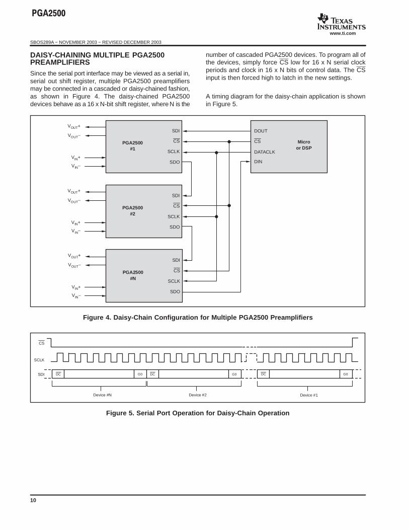
DAISY-CHAINING MULTIPLE PGA2500PREAMPLIFIERSSince the serial port interface may be viewed as a serial in,serial out shift register, multiple PGA2500 preamplifiersmay be connected in a cascaded or daisy-chained fashion,as shown in Figure 4. The daisy-chained PGA2500devices behave as a 16 x N-bit shift register, where N is the
number of cascaded PGA2500 devices. To program all ofthe devices, simply force CS low for 16 x N serial clockperiods and clock in 16 x N bits of control data. The CSinput is then forced high to latch in the new settings.
A timing diagram for the daisy-chain application is shownin Figure 5.
CS
SCLK
SDI
SDO
VOUT+
VOUT−
VIN+
VIN−
PGA2500#1
CS
SCLK
SDI
SDO
VOUT+
VOUT−
VIN+
VIN−
PGA2500#2
CS
SCLK
SDI
SDO
VOUT+
VOUT−
VIN+
VIN−
PGA2500#N
CS
DATACLK
DOUT
DIN
Microor DSP
Figure 4. Daisy-Chain Configuration for Multiple PGA2500 Preamplifiers
SCLK
CS
SDI DC G0DC G0DC
Device #1Device #2Device #N
G0
Figure 5. Serial Port Operation for Daisy-Chain Operation

"#$%%
SBOS289A − NOVEMBER 2003 − REVISED DECEMBER 2003
www.ti.com
11
APPLICATION INFORMATIONThis section provides practical information for designingthe PGA2500 into end applications.
BASIC CIRCUIT CONFIGURATIONA typical applications circuit, without the input and outputcircuitry, is shown in Figure 6. Power-supply bypass andDC servo capacitors are shown with recommendedvalues. All capacitors should be placed as close aspossible to the PGA2500 package to limit inductive noisecoupling. Surface-mount capacitors are recommended(X7R ceramic for the 0.1µF and 1µF capacitors, and lowESR tantalum for the 4.7µF capacitors).
The PGA2500 can be placed on a split ground plane, withthe package located over the split. However, there must bea low impedance connection between the analog anddigital grounds at a common return point.
The DC common-mode input, VCOMIN (pin 25), can beconnected to analog ground or a DC voltage (such as thereference or common voltage output of an audio ADC).When biasing this input to a DC voltage, keep in mind thatboth the analog output and input pins are level-shifted bythe value of the bias voltage.
GPO1
GPO2
GPO3
GPO4
OVR
1
2
3
4
5
PGA2500
ToRelay Drivers,
Switches, or Indicators
AGND28
DGND6
To/FromMPU, MCU,
DSP, or Logic
DCEN
0dB
ZCEN
SDI
CS
SCLK
VOUT+
VOUT−
10
11
12
VD−14
VA−15
ToAnalog OutputCircuit
17
16
VIN+
VIN−
FromAnalog InputCircuit To
OptionalCommon−ModeVoltage0Ω(1)
27
26
SDO13
7
8
9
CS21
CS22
22
21
10Ω
0.1µF
VA−
VA−
200.1µF
0.1µF
+4.7µF
+4.7µF
VA−19
0.1µF
1µF
CS11
CS12
24
23
1µF
VA−
VA+
180.1µF
+4.7µF
VCOMIN25
= Analog Ground
= Digital Ground
0.1µF(1)
NOTE: (1) Install a 0Ω shunt or jumper only when connecting VCOMINto analog ground. Install a 0.1µF ceramic capacitor (X7R type) onlywhen connecting VCOMIN to a DC common−mode voltage source.
Connect Digital and Analog Grounds atone common return point in the circuit.
Figure 6. Basic Circuit Configuration for the PGA2500
"#$%%
SBOS289A − NOVEMBER 2003 − REVISED DECEMBER 2003
www.ti.com
12
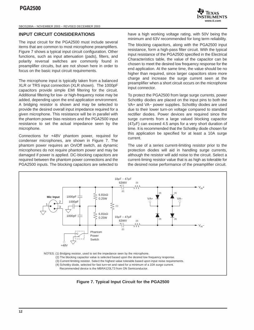
INPUT CIRCUIT CONSIDERATIONS
The input circuit for the PGA2500 must include severalitems that are common to most microphone preamplifiers.Figure 7 shows a typical input circuit configuration. Otherfunctions, such as input attenuation (pads), filters, andpolarity reversal switches are commonly found inpreamplifier circuits, but are not shown here in order tofocus on the basic input circuit requirements.
The microphone input is typically taken from a balancedXLR or TRS input connection (XLR shown). The 1000pFcapacitors provide simple EMI filtering for the circuit.Additional filtering for low- or high-frequency noise may beadded, depending upon the end application environment.A bridging resistor is shown and may be selected toprovide the desired overall input impedance required for agiven microphone. This resistance will be in parallel withthe phantom power bias resistors and the PGA2500 inputresistance to set the actual impedance seen by themicrophone.
Connections for +48V phantom power, required forcondenser microphones, are shown in Figure 7. Thephantom power requires an On/Off switch, as dynamicmicrophones do not require phantom power and may bedamaged if power is applied. DC-blocking capacitors arerequired between the phantom power connections and thePGA2500 inputs. The blocking capacitors are selected to
have a high working voltage rating, with 50V being theminimum and 63V recommended for long term reliability.
The blocking capacitors, along with the PGA2500 inputresistance, form a high-pass filter circuit. With the typicalinput resistance of the PGA2500 specified in the ElectricalCharacteristics table, the value of the capacitor can bechosen to meet the desired low frequency response for theend application. At the same time, the value should be nohigher than required, since larger capacitors store morecharge and increase the surge current seen at thepreamplifier when a short circuit occurs on the microphoneinput connector.
To protect the PGA2500 from large surge currents, powerSchottky diodes are placed on the input pins to both theVA+ and VA− power supplies. Schottky diodes are useddue to their lower turn-on voltage compared to standardrectifier diodes. Power devices are required since thesurge currents from a large valued blocking capacitor(47µF) can exceed 4.5 amps for a very short duration oftime. It is recommended that the Schottky diode chosen forthis application be specified for at least a 10A surgecurrent.
The use of a series current-limiting resistor prior to theprotection diodes will aid in handling surge currents,although the resistor will add noise to the circuit. Select acurrent-liming resistor value that is as high as tolerable forthe desired noise performance of the preamplifier circuit.
(3)
6.81kΩ0.25W
(4) (4)
(4) (4)
(3)
10µF − 47µF63WV+
+
10µF − 47µF63WV
1
Mic Input
2
3
1000pF
1000pF
1000pF
6.81kΩ0.25W
PhantomPowerSwitch
+48V
(1)
(2)
(2)
VA+ VA−
VIN+
VIN−
NOTES: (1) Bridging resistor, used to set the impedance seen by the microphone.(2) The blocking capacitor value is selected based upon the desired low frequency response.(3) Current−limiting resistor. Select the highest value tolerable based upon input noise requirements.(4) Schottky diode, selected for fast turn−on and rated for a minimum of a 10A surge current.
Recommended device is the MBRA120LT3 from ON Semiconductor.
Figure 7. Typical Input Circuit for the PGA2500
"#$%%
SBOS289A − NOVEMBER 2003 − REVISED DECEMBER 2003
www.ti.com
13
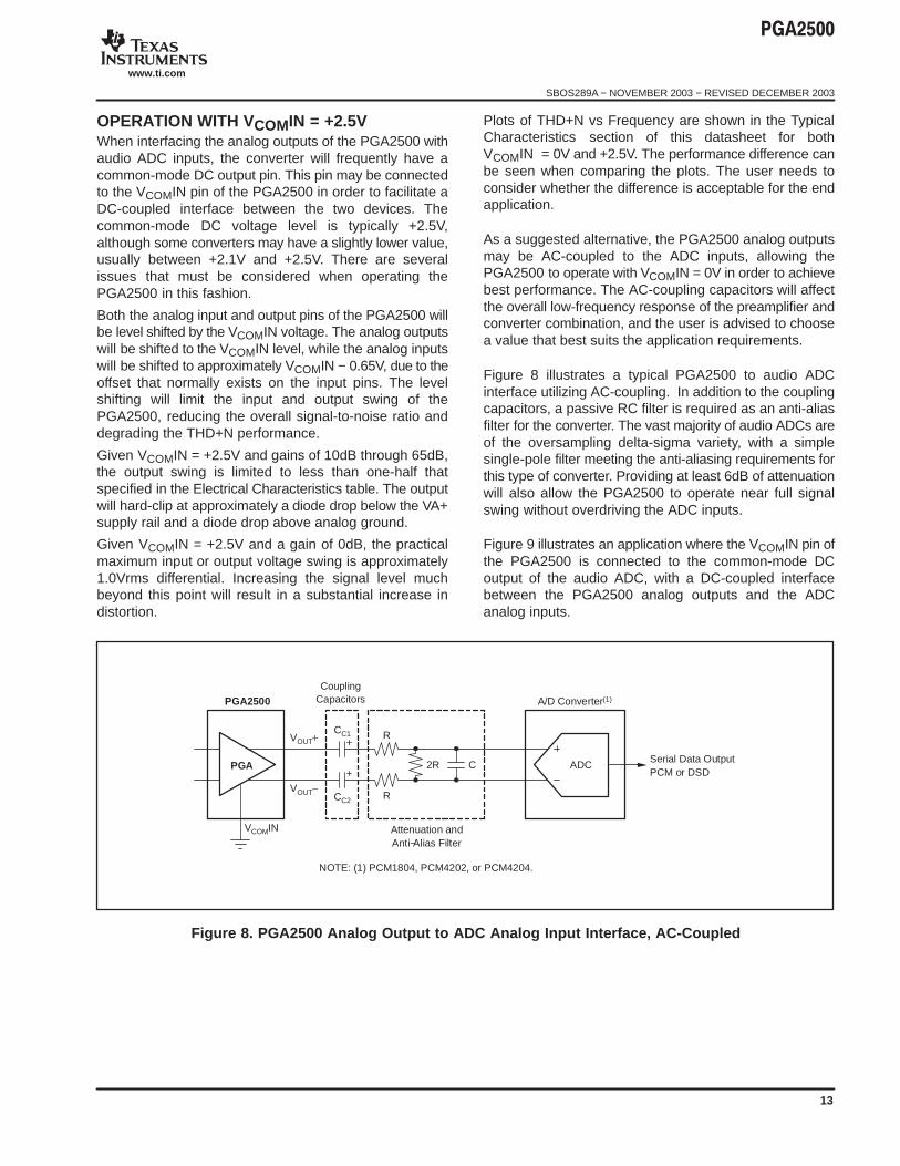
OPERATION WITH VCOMIN = +2.5VWhen interfacing the analog outputs of the PGA2500 withaudio ADC inputs, the converter will frequently have acommon-mode DC output pin. This pin may be connectedto the VCOMIN pin of the PGA2500 in order to facilitate aDC-coupled interface between the two devices. Thecommon-mode DC voltage level is typically +2.5V,although some converters may have a slightly lower value,usually between +2.1V and +2.5V. There are severalissues that must be considered when operating thePGA2500 in this fashion.
Both the analog input and output pins of the PGA2500 willbe level shifted by the VCOMIN voltage. The analog outputswill be shifted to the VCOMIN level, while the analog inputswill be shifted to approximately VCOMIN − 0.65V, due to theoffset that normally exists on the input pins. The levelshifting will limit the input and output swing of thePGA2500, reducing the overall signal-to-noise ratio anddegrading the THD+N performance.
Given VCOMIN = +2.5V and gains of 10dB through 65dB,the output swing is limited to less than one-half thatspecified in the Electrical Characteristics table. The outputwill hard-clip at approximately a diode drop below the VA+supply rail and a diode drop above analog ground.
Given VCOMIN = +2.5V and a gain of 0dB, the practicalmaximum input or output voltage swing is approximately1.0Vrms differential. Increasing the signal level muchbeyond this point will result in a substantial increase indistortion.
Plots of THD+N vs Frequency are shown in the TypicalCharacteristics section of this datasheet for bothVCOMIN = 0V and +2.5V. The performance difference canbe seen when comparing the plots. The user needs toconsider whether the difference is acceptable for the endapplication.
As a suggested alternative, the PGA2500 analog outputsmay be AC-coupled to the ADC inputs, allowing thePGA2500 to operate with VCOMIN = 0V in order to achievebest performance. The AC-coupling capacitors will affectthe overall low-frequency response of the preamplifier andconverter combination, and the user is advised to choosea value that best suits the application requirements.
Figure 8 illustrates a typical PGA2500 to audio ADCinterface utilizing AC-coupling. In addition to the couplingcapacitors, a passive RC filter is required as an anti-aliasfilter for the converter. The vast majority of audio ADCs areof the oversampling delta-sigma variety, with a simplesingle-pole filter meeting the anti-aliasing requirements forthis type of converter. Providing at least 6dB of attenuationwill also allow the PGA2500 to operate near full signalswing without overdriving the ADC inputs.
Figure 9 illustrates an application where the VCOMIN pin ofthe PGA2500 is connected to the common-mode DCoutput of the audio ADC, with a DC-coupled interfacebetween the PGA2500 analog outputs and the ADCanalog inputs.
R
R
2R CPGA
PGA2500
CC1
CC2
VOUT+
VOUT−
VCOMIN
ADC
A/D Converter(1)
+
+Serial Data OutputPCM or DSD
CouplingCapacitors
Attenuation andAnti−Alias Filter
NOTE: (1) PCM1804, PCM4202, or PCM4204.
Figure 8. PGA2500 Analog Output to ADC Analog Input Interface, AC-Coupled

"#$%%
SBOS289A − NOVEMBER 2003 − REVISED DECEMBER 2003
www.ti.com
14
R
R
C
0.1µF
PGA
PGA2500
VOUT+
VOUT−
VCOMIN VCOM Output
ADC
A/D Converter(1)
Serial Data OutputPCM or DSD
Anti−Alias Filter
NOTE: (1) PCM1804, PCM4202, or PCM4204.
Figure 9. PGA2500 Analog Output to ADC Analog Input Interface, DC-Coupled
PACKAGE OPTION ADDENDUM
www.ti.com 10-Dec-2020
Addendum-Page 1
PACKAGING INFORMATION
Orderable Device Status(1)
Package Type PackageDrawing
Pins PackageQty
Eco Plan(2)
Lead finish/Ball material
(6)
MSL Peak Temp(3)
Op Temp (°C) Device Marking(4/5)
Samples
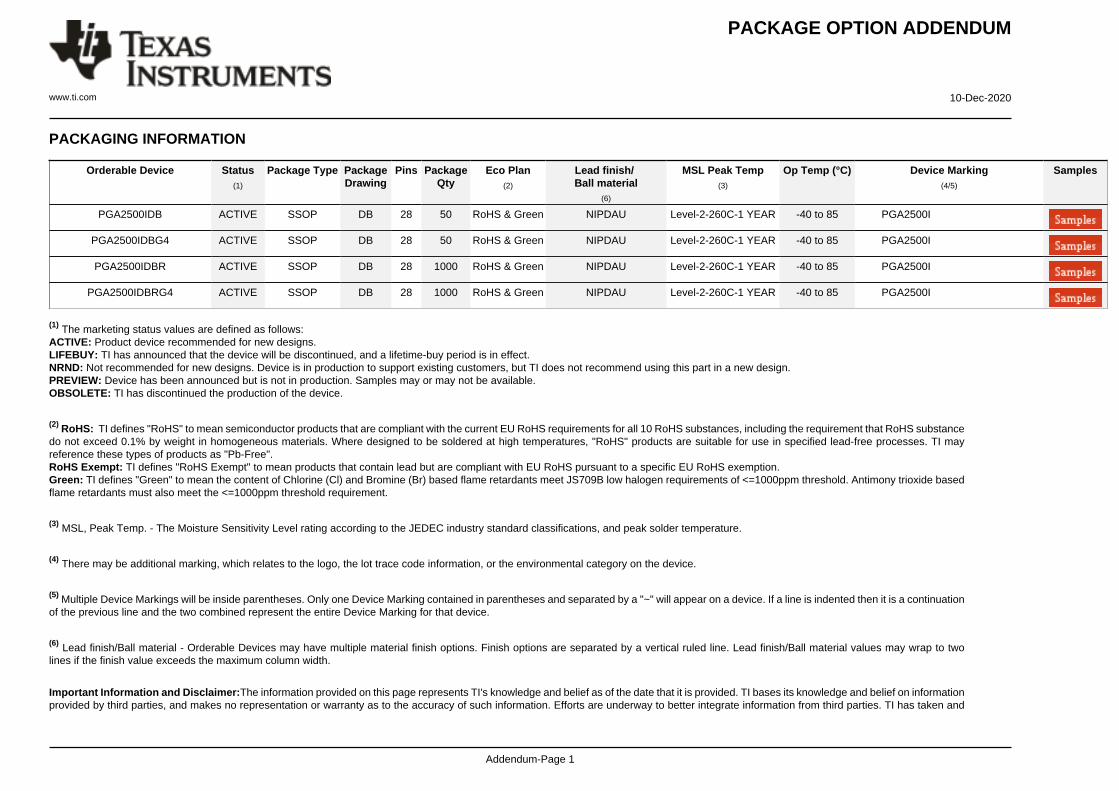
PGA2500IDB ACTIVE SSOP DB 28 50 RoHS & Green NIPDAU Level-2-260C-1 YEAR -40 to 85 PGA2500I
PGA2500IDBG4 ACTIVE SSOP DB 28 50 RoHS & Green NIPDAU Level-2-260C-1 YEAR -40 to 85 PGA2500I
PGA2500IDBR ACTIVE SSOP DB 28 1000 RoHS & Green NIPDAU Level-2-260C-1 YEAR -40 to 85 PGA2500I
PGA2500IDBRG4 ACTIVE SSOP DB 28 1000 RoHS & Green NIPDAU Level-2-260C-1 YEAR -40 to 85 PGA2500I
(1) The marketing status values are defined as follows:ACTIVE: Product device recommended for new designs.LIFEBUY: TI has announced that the device will be discontinued, and a lifetime-buy period is in effect.NRND: Not recommended for new designs. Device is in production to support existing customers, but TI does not recommend using this part in a new design.PREVIEW: Device has been announced but is not in production. Samples may or may not be available.OBSOLETE: TI has discontinued the production of the device.
(2) RoHS: TI defines "RoHS" to mean semiconductor products that are compliant with the current EU RoHS requirements for all 10 RoHS substances, including the requirement that RoHS substancedo not exceed 0.1% by weight in homogeneous materials. Where designed to be soldered at high temperatures, "RoHS" products are suitable for use in specified lead-free processes. TI mayreference these types of products as "Pb-Free".RoHS Exempt: TI defines "RoHS Exempt" to mean products that contain lead but are compliant with EU RoHS pursuant to a specific EU RoHS exemption.Green: TI defines "Green" to mean the content of Chlorine (Cl) and Bromine (Br) based flame retardants meet JS709B low halogen requirements of <=1000ppm threshold. Antimony trioxide basedflame retardants must also meet the <=1000ppm threshold requirement.
(3) MSL, Peak Temp. - The Moisture Sensitivity Level rating according to the JEDEC industry standard classifications, and peak solder temperature.
(4) There may be additional marking, which relates to the logo, the lot trace code information, or the environmental category on the device.
(5) Multiple Device Markings will be inside parentheses. Only one Device Marking contained in parentheses and separated by a "~" will appear on a device. If a line is indented then it is a continuationof the previous line and the two combined represent the entire Device Marking for that device.
(6) Lead finish/Ball material - Orderable Devices may have multiple material finish options. Finish options are separated by a vertical ruled line. Lead finish/Ball material values may wrap to twolines if the finish value exceeds the maximum column width.
Important Information and Disclaimer:The information provided on this page represents TI's knowledge and belief as of the date that it is provided. TI bases its knowledge and belief on informationprovided by third parties, and makes no representation or warranty as to the accuracy of such information. Efforts are underway to better integrate information from third parties. TI has taken and

PACKAGE OPTION ADDENDUM
www.ti.com 10-Dec-2020
Addendum-Page 2
continues to take reasonable steps to provide representative and accurate information but may not have conducted destructive testing or chemical analysis on incoming materials and chemicals.TI and TI suppliers consider certain information to be proprietary, and thus CAS numbers and other limited information may not be available for release.
In no event shall TI's liability arising out of such information exceed the total purchase price of the TI part(s) at issue in this document sold by TI to Customer on an annual basis.

PACKAGE MATERIALS INFORMATION
www.ti.com 3-Jun-2022
TAPE AND REEL INFORMATION
Reel Width (W1)
REEL DIMENSIONS
A0B0K0W
Dimension designed to accommodate the component lengthDimension designed to accommodate the component thicknessOverall width of the carrier tapePitch between successive cavity centers
Dimension designed to accommodate the component width
TAPE DIMENSIONS
K0 P1
B0 W
A0Cavity
QUADRANT ASSIGNMENTS FOR PIN 1 ORIENTATION IN TAPE
Pocket Quadrants
Sprocket Holes
Q1 Q1Q2 Q2
Q3 Q3Q4 Q4 User Direction of Feed
P1
ReelDiameter
*All dimensions are nominal
Device PackageType
PackageDrawing
Pins SPQ ReelDiameter
(mm)
ReelWidth
W1 (mm)
A0(mm)
B0(mm)
K0(mm)
P1(mm)
W(mm)
Pin1Quadrant
PGA2500IDBR SSOP DB 28 1000 330.0 16.4 8.2 10.5 2.5 12.0 16.0 Q1
Pack Materials-Page 1

PACKAGE MATERIALS INFORMATION
www.ti.com 3-Jun-2022
TAPE AND REEL BOX DIMENSIONS
Width (mm)
W L
H
*All dimensions are nominal
Device Package Type Package Drawing Pins SPQ Length (mm) Width (mm) Height (mm)
PGA2500IDBR SSOP DB 28 1000 356.0 356.0 35.0
Pack Materials-Page 2

PACKAGE MATERIALS INFORMATION
www.ti.com 3-Jun-2022
TUBE
L - Tube lengthT - Tube height
W - Tube width
B - Alignment groove width *All dimensions are nominal
Device Package Name Package Type Pins SPQ L (mm) W (mm) T (µm) B (mm)
PGA2500IDB DB SSOP 28 50 530 10.5 4000 4.1
PGA2500IDBG4 DB SSOP 28 50 530 10.5 4000 4.1
Pack Materials-Page 3

www.ti.com
PACKAGE OUTLINE
C
26X 0.65
2X8.45
28X 0.380.22
8.27.4 TYP
SEATINGPLANE
0.05 MIN
0.25GAGE PLANE
0 -8
2 MAX
B 5.65.0
NOTE 4
A
10.59.9
NOTE 3
0.950.55
(0.15) TYP
SSOP - 2 mm max heightDB0028ASMALL OUTLINE PACKAGE
4214853/B 03/2018
1
1415
28
0.15 C A B
PIN 1 INDEX AREA
SEE DETAIL A
0.1 C
NOTES: 1. All linear dimensions are in millimeters. Any dimensions in parenthesis are for reference only. Dimensioning and tolerancing per ASME Y14.5M. 2. This drawing is subject to change without notice. 3. This dimension does not include mold flash, protrusions, or gate burrs. Mold flash, protrusions, or gate burrs shall not exceed 0.15 mm per side. 4. This dimension does not include interlead flash. Interlead flash shall not exceed 0.25 mm per side.5. Reference JEDEC registration MO-150.
A 15DETAIL ATYPICAL
SCALE 1.500

www.ti.com
EXAMPLE BOARD LAYOUT
0.07 MAXALL AROUND
0.07 MINALL AROUND
28X (1.85)
28X (0.45)
26X (0.65)
(7)
(R0.05) TYP
SSOP - 2 mm max heightDB0028ASMALL OUTLINE PACKAGE
4214853/B 03/2018
NOTES: (continued) 6. Publication IPC-7351 may have alternate designs. 7. Solder mask tolerances between and around signal pads can vary based on board fabrication site.
LAND PATTERN EXAMPLEEXPOSED METAL SHOWN
SCALE: 10X
SYMM
SYMM
1
14 15
28
15.000
METALSOLDER MASKOPENING
METAL UNDERSOLDER MASK
SOLDER MASKOPENING
EXPOSED METALEXPOSED METAL
SOLDER MASK DETAILS
NON-SOLDER MASKDEFINED
(PREFERRED)
SOLDER MASKDEFINED

www.ti.com
EXAMPLE STENCIL DESIGN
28X (1.85)
28X (0.45)
26X (0.65)
(7)
(R0.05) TYP
SSOP - 2 mm max heightDB0028ASMALL OUTLINE PACKAGE
4214853/B 03/2018
NOTES: (continued) 8. Laser cutting apertures with trapezoidal walls and rounded corners may offer better paste release. IPC-7525 may have alternate design recommendations. 9. Board assembly site may have different recommendations for stencil design.
SOLDER PASTE EXAMPLEBASED ON 0.125 mm THICK STENCIL
SCALE: 10X
SYMM
SYMM
1
14 15
28

IMPORTANT NOTICE AND DISCLAIMERTI PROVIDES TECHNICAL AND RELIABILITY DATA (INCLUDING DATA SHEETS), DESIGN RESOURCES (INCLUDING REFERENCE DESIGNS), APPLICATION OR OTHER DESIGN ADVICE, WEB TOOLS, SAFETY INFORMATION, AND OTHER RESOURCES “AS IS” AND WITH ALL FAULTS, AND DISCLAIMS ALL WARRANTIES, EXPRESS AND IMPLIED, INCLUDING WITHOUT LIMITATION ANY IMPLIED WARRANTIES OF MERCHANTABILITY, FITNESS FOR A PARTICULAR PURPOSE OR NON-INFRINGEMENT OF THIRD PARTY INTELLECTUAL PROPERTY RIGHTS.These resources are intended for skilled developers designing with TI products. You are solely responsible for (1) selecting the appropriate TI products for your application, (2) designing, validating and testing your application, and (3) ensuring your application meets applicable standards, and any other safety, security, regulatory or other requirements.These resources are subject to change without notice. TI grants you permission to use these resources only for development of an application that uses the TI products described in the resource. Other reproduction and display of these resources is prohibited. No license is granted to any other TI intellectual property right or to any third party intellectual property right. TI disclaims responsibility for, and you will fully indemnify TI and its representatives against, any claims, damages, costs, losses, and liabilities arising out of your use of these resources.TI’s products are provided subject to TI’s Terms of Sale or other applicable terms available either on ti.com or provided in conjunction with such TI products. TI’s provision of these resources does not expand or otherwise alter TI’s applicable warranties or warranty disclaimers for TI products.TI objects to and rejects any additional or different terms you may have proposed. IMPORTANT NOTICE
Mailing Address: Texas Instruments, Post Office Box 655303, Dallas, Texas 75265Copyright © 2022, Texas Instruments Incorporated
Copyright © 2022 FDOKUMEN