Performance and Analysis of Voltage Scaled Repeaters for ...
6
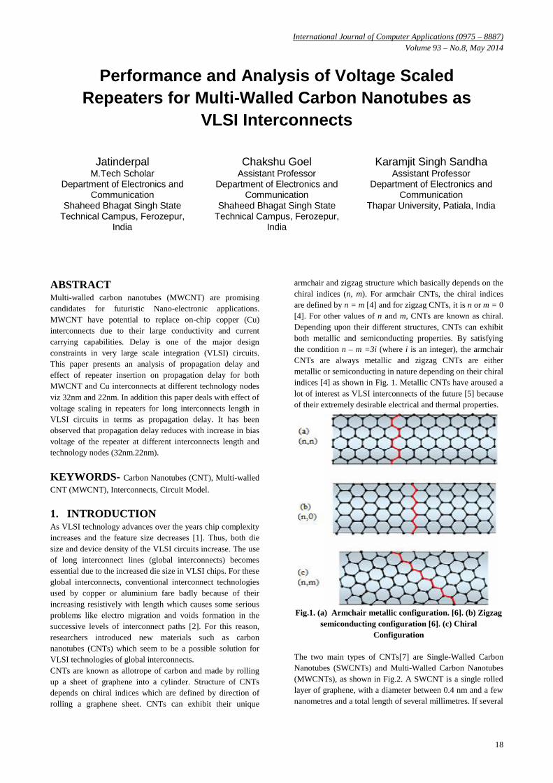
International Journal of Computer Applications (0975 – 8887) Volume 93 – No.8, May 2014 18 Performance and Analysis of Voltage Scaled Repeaters for Multi-Walled Carbon Nanotubes as VLSI Interconnects Jatinderpal M.Tech Scholar Department of Electronics and Communication Shaheed Bhagat Singh State Technical Campus, Ferozepur, India Chakshu Goel Assistant Professor Department of Electronics and Communication Shaheed Bhagat Singh State Technical Campus, Ferozepur, India Karamjit Singh Sandha Assistant Professor Department of Electronics and Communication Thapar University, Patiala, India ABSTRACT Multi-walled carbon nanotubes (MWCNT) are promising candidates for futuristic Nano-electronic applications. MWCNT have potential to replace on-chip copper (Cu) interconnects due to their large conductivity and current carrying capabilities. Delay is one of the major design constraints in very large scale integration (VLSI) circuits. This paper presents an analysis of propagation delay and effect of repeater insertion on propagation delay for both MWCNT and Cu interconnects at different technology nodes viz 32nm and 22nm. In addition this paper deals with effect of voltage scaling in repeaters for long interconnects length in VLSI circuits in terms as propagation delay. It has been observed that propagation delay reduces with increase in bias voltage of the repeater at different interconnects length and technology nodes (32nm.22nm). KEYWORDS- Carbon Nanotubes (CNT), Multi-walled CNT (MWCNT), Interconnects, Circuit Model. 1. INTRODUCTION As VLSI technology advances over the years chip complexity increases and the feature size decreases [1]. Thus, both die size and device density of the VLSI circuits increase. The use of long interconnect lines (global interconnects) becomes essential due to the increased die size in VLSI chips. For these global interconnects, conventional interconnect technologies used by copper or aluminium fare badly because of their increasing resistively with length which causes some serious problems like electro migration and voids formation in the successive levels of interconnect paths [2]. For this reason, researchers introduced new materials such as carbon nanotubes (CNTs) which seem to be a possible solution for VLSI technologies of global interconnects. CNTs are known as allotrope of carbon and made by rolling up a sheet of graphene into a cylinder. Structure of CNTs depends on chiral indices which are defined by direction of rolling a graphene sheet. CNTs can exhibit their unique armchair and zigzag structure which basically depends on the chiral indices (n, m). For armchair CNTs, the chiral indices are defined by n = m [4] and for zigzag CNTs, it is n or m = 0 [4]. For other values of n and m, CNTs are known as chiral. Depending upon their different structures, CNTs can exhibit both metallic and semiconducting properties. By satisfying the condition n – m =3i (where i is an integer), the armchair CNTs are always metallic and zigzag CNTs are either metallic or semiconducting in nature depending on their chiral indices [4] as shown in Fig. 1. Metallic CNTs have aroused a lot of interest as VLSI interconnects of the future [5] because of their extremely desirable electrical and thermal properties. Fig.1. (a) Armchair metallic configuration. [6]. (b) Zigzag semiconducting configuration [6]. (c) Chiral Configuration The two main types of CNTs[7] are Single-Walled Carbon Nanotubes (SWCNTs) and Multi-Walled Carbon Nanotubes (MWCNTs), as shown in Fig.2. A SWCNT is a single rolled layer of graphene, with a diameter between 0.4 nm and a few nanometres and a total length of several millimetres. If several
-
Upload
khangminh22 -
Category
Documents
-
view
1 -
download
0
Transcript of Performance and Analysis of Voltage Scaled Repeaters for ...
International Journal of Computer Applications (0975 – 8887)
Volume 93 – No.8, May 2014
18
Performance and Analysis of Voltage Scaled
Repeaters for Multi-Walled Carbon Nanotubes as
VLSI Interconnects
Jatinderpal M.Tech Scholar
Department of Electronics and Communication
Shaheed Bhagat Singh State Technical Campus, Ferozepur,
India
Chakshu Goel Assistant Professor
Department of Electronics and Communication
Shaheed Bhagat Singh State Technical Campus, Ferozepur,
India
Karamjit Singh Sandha Assistant Professor
Department of Electronics and Communication
Thapar University, Patiala, India
ABSTRACT Multi-walled carbon nanotubes (MWCNT) are promising
candidates for futuristic Nano-electronic applications.
MWCNT have potential to replace on-chip copper (Cu)
interconnects due to their large conductivity and current
carrying capabilities. Delay is one of the major design
constraints in very large scale integration (VLSI) circuits.
This paper presents an analysis of propagation delay and
effect of repeater insertion on propagation delay for both
MWCNT and Cu interconnects at different technology nodes
viz 32nm and 22nm. In addition this paper deals with effect of
voltage scaling in repeaters for long interconnects length in
VLSI circuits in terms as propagation delay. It has been
observed that propagation delay reduces with increase in bias
voltage of the repeater at different interconnects length and
technology nodes (32nm.22nm).
KEYWORDS- Carbon Nanotubes (CNT), Multi-walled
CNT (MWCNT), Interconnects, Circuit Model.
1. INTRODUCTION As VLSI technology advances over the years chip complexity
increases and the feature size decreases [1]. Thus, both die
size and device density of the VLSI circuits increase. The use
of long interconnect lines (global interconnects) becomes
essential due to the increased die size in VLSI chips. For these
global interconnects, conventional interconnect technologies
used by copper or aluminium fare badly because of their
increasing resistively with length which causes some serious
problems like electro migration and voids formation in the
successive levels of interconnect paths [2]. For this reason,
researchers introduced new materials such as carbon
nanotubes (CNTs) which seem to be a possible solution for
VLSI technologies of global interconnects.
CNTs are known as allotrope of carbon and made by rolling
up a sheet of graphene into a cylinder. Structure of CNTs
depends on chiral indices which are defined by direction of
rolling a graphene sheet. CNTs can exhibit their unique
armchair and zigzag structure which basically depends on the
chiral indices (n, m). For armchair CNTs, the chiral indices
are defined by n = m [4] and for zigzag CNTs, it is n or m = 0
[4]. For other values of n and m, CNTs are known as chiral.
Depending upon their different structures, CNTs can exhibit
both metallic and semiconducting properties. By satisfying
the condition n – m =3i (where i is an integer), the armchair
CNTs are always metallic and zigzag CNTs are either
metallic or semiconducting in nature depending on their chiral
indices [4] as shown in Fig. 1. Metallic CNTs have aroused a
lot of interest as VLSI interconnects of the future [5] because
of their extremely desirable electrical and thermal properties.
Fig.1. (a) Armchair metallic configuration. [6]. (b) Zigzag
semiconducting configuration [6]. (c) Chiral
Configuration
The two main types of CNTs[7] are Single-Walled Carbon
Nanotubes (SWCNTs) and Multi-Walled Carbon Nanotubes
(MWCNTs), as shown in Fig.2. A SWCNT is a single rolled
layer of graphene, with a diameter between 0.4 nm and a few
nanometres and a total length of several millimetres. If several
International Journal of Computer Applications (0975 – 8887)
Volume 93 – No.8, May 2014
19
SWCNTs with varying diameter are nested concentrically
inside one another, the resulting structure is called a multi-
walled carbon nanotube (MWCNT).[5]
Fig. 2. Structure of a single layer of graphite (graphene)
(left), single-walled
carbon nanotube (SWCNT) as a rolled-up graphene sheet
(middle) and a multi-walled nanotube with three concentric
shells (right).
This paper is organized as follows. The following Section 2
presents a discussion for a Cu interconnect and describes the
models used for evaluating interconnect performance. Section
3 describes the equivalent circuit model for a MWCNT that is
useful in the performance analysis of MWCNT interconnects
and discusses existing work in the literature that compare
MWCNT interconnects with copper. Section 4 analyses the
impact of the repeaters on the performance of interconnects.
Section 5 analyzes the impact of the voltage scaled repeater
on the performance in terms of delay of interconnects. The
results of the analysis of MWCNT and Cu interconnects are
compared Section 6 and the lessons learned are summarized
in Section 7.
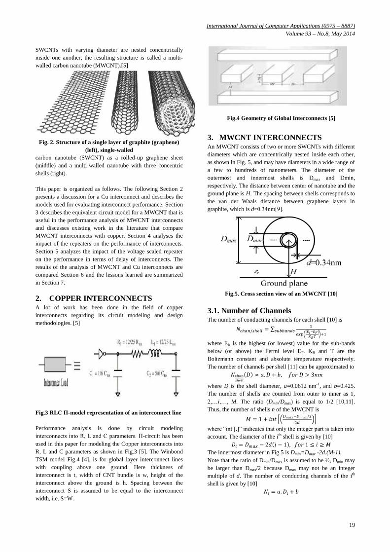
2. COPPER INTERCONNECTS A lot of work has been done in the field of copper
interconnects regarding its circuit modeling and design
methodologies. [5]
Fig.3 RLC Π-model representation of an interconnect line
Performance analysis is done by circuit modeling
interconnects into R, L and C parameters. Π-circuit has been
used in this paper for modeling the Copper interconnects into
R, L and C parameters as shown in Fig.3 [5]. The Winbond
TSM model Fig.4 [4], is for global layer interconnect lines
with coupling above one ground. Here thickness of
interconnect is t, width of CNT bundle is w, height of the
interconnect above the ground is h. Spacing between the
interconnect S is assumed to be equal to the interconnect
width, i.e. S=W.
Fig.4 Geometry of Global Interconnects [5]
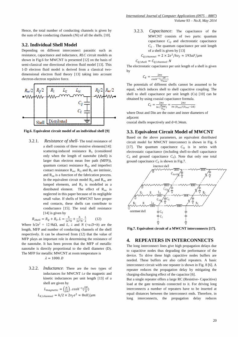
3. MWCNT INTERCONNECTS An MWCNT consists of two or more SWCNTs with different
diameters which are concentrically nested inside each other,
as shown in Fig. 5, and may have diameters in a wide range of
a few to hundreds of nanometers. The diameter of the
outermost and innermost shells is Dmax and Dmin,
respectively. The distance between center of nanotube and the
ground plane is H. The spacing between shells corresponds to
the van der Waals distance between graphene layers in
graphite, which is d≈0.34nm[9].
Fig.5. Cross section view of an MWCNT [10]
3.1. Number of Channels The number of conducting channels for each shell [10] is
where Ei, is the highest (or lowest) value for the sub-bands
below (or above) the Fermi level EF. KB and T are the
Boltzmann constant and absolute temperature respectively.
The number of channels per shell [11] can be approximated to
where D is the shell diameter, a=0.0612 nm-1, and b=0.425.
The number of shells are counted from outer to inner as 1,
2,…i,…, M. The ratio (Dmin/Dmax) is equal to 1/2 [10,11].
Thus, the number of shells n of the MWCNT is
where “int [.]” indicates that only the integer part is taken into
account. The diameter of the ith shell is given by [10]
The innermost diameter in Fig.5 is Dmin=Dmax -2d.(M-1).
Note that the ratio of Dmin/Dmax is assumed to be ½, Dmin may
be larger than Dmax/2 because Dmax may not be an integer
multiple of d. The number of conducting channels of the ith
shell is given by [10]
International Journal of Computer Applications (0975 – 8887)
Volume 93 – No.8, May 2014
20
Hence, the total number of conducting channels is given by
the sum of the conducting channels (Ni) of all the shells. [10].
3.2. Individual Shell Model Depending on different interconnect parasitic such as
resistance, capacitance and inductance, RLC circuit models as
shown in Fig.6 for MWCNT is presented [12] on the basis of
semi-classical one directional electron fluid model [13]. This
1-D electron fluid model is derived from a classical two-
dimensional electron fluid theory [13] taking into account
electron-electron repulsive force.
Fig.6. Equivalent circuit model of an individual shell [9]
3.2.1. Resistance of shell- The total resistance of
a shell consists of three resistive elements[14]:
scattering-induced resistance RS (considered
only when the length of nanotube (shell) is
larger than electron mean free path (MFP)),
quantum contact resistance RQ, and imperfect
contact resistance Rmc. RQ and RS are intrinsic,
and Rmc is a function of the fabrication process.
In the equivalent circuit model RQ and Rmc are
lumped elements, and RS is modelled as a
distributed element. The effect of Rmc is
neglected in this paper because of its negligible
small value. If shells of MWCNT have proper
end contacts, these shells can contribute to
conductance [15]. The total shell resistance
[14] is given by
(12)
Where h/2e2 = 12.9kΩ, and L, λ and N (=a.D+b) are the
length, MFP and number of conducting channels of the shell
respectively. It can be observed from (12) that the value of
MFP plays an important role in determining the resistance of
the nanotube. It has been proven that the MFP of metallic
nanotube is directly proportional to the shell diameter (D).
The MFP for metallic MWCNT at room temperature is
3.2.2. Inductance: There are the two types of
inductances for MWCNT i.e the magnetic and
kinetic inductances per unit length [13] of a
shell are given by
3.2.3. Capacitance: The capacitance of the
MWCNT consists of two parts: quantum
capacitance CQ and electrostatic capacitance
CE . The quantum capacitance per unit length
of a shell is given by [13]
The electrostatic capacitance per unit length of a shell is given
by
The potentials of different shells cannot be assumed to be
equal, which induces shell to shell capacitive coupling. The
shell to shell capacitance per unit length (Cs) [10] can be
obtained by using coaxial capacitance formula.
where Dout and Din are the outer and inner diameters of
adjacent
coaxial shells respectively and d=0.34nm.
3.3. Equivalent Circuit Model of MWCNT Based on the above parameters, an equivalent distributed
circuit model for MWCNT interconnect is shown in Fig. 6
[17]. The quantum capacitance CQ is in series with
electrostatic capacitance (including shell-to-shell capacitance
CS and ground capacitance CE). Note that only one total
ground capacitance CE is shown in Fig.7.
Fig.7. Equivalent circuit of a MWCNT interconnects [17].
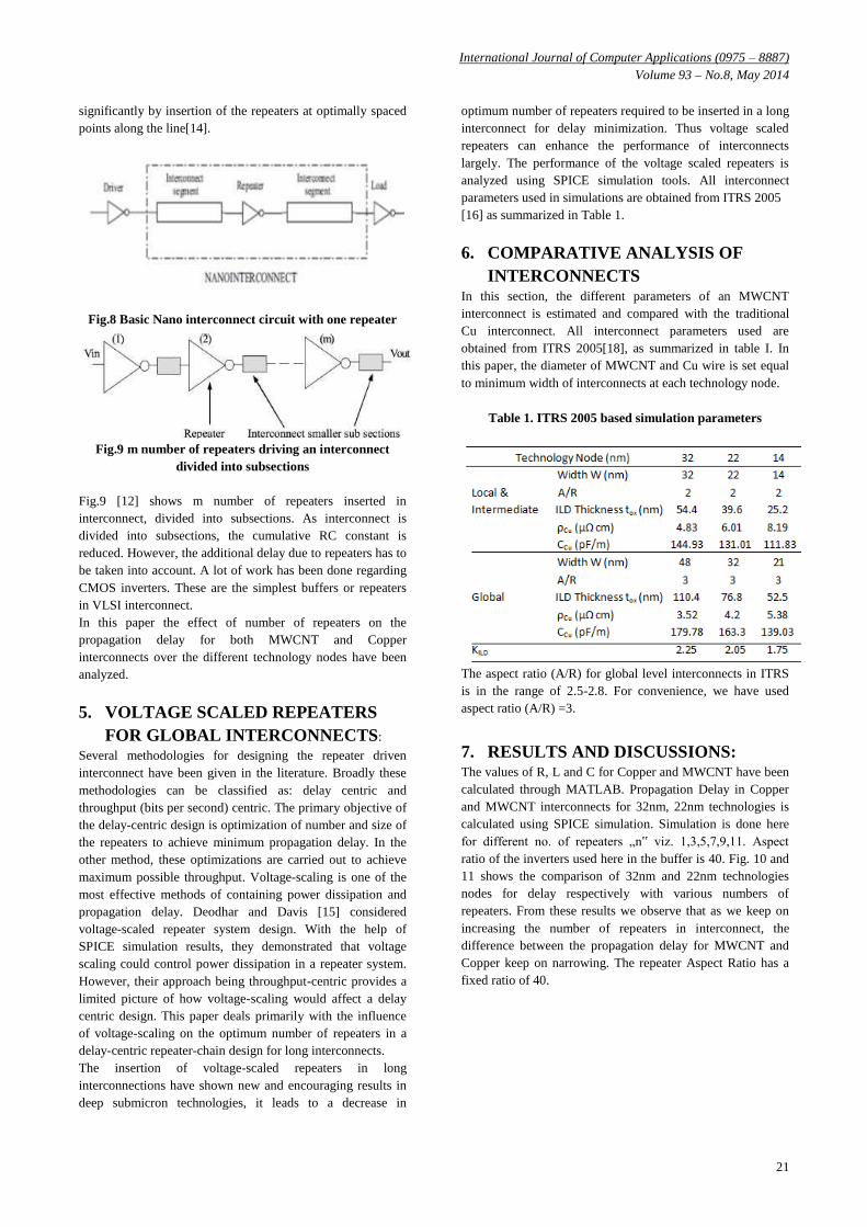
4. REPEATERS IN INTERCONNECTS The long interconnect lines give high propagation delays due
to capacitive nodes thus degrading the performance of the
device. To drive these high capacitive nodes buffers are
needed. These buffers are also called repeaters. A basic
interconnect circuit with one repeater is shown in Fig. 8 [6]. A
repeater reduces the propagation delay by mitigating the
charging-discharging effect of the capacitor [6].
But a single repeater offers a large RC (Resistive- Capacitive)
load at the gate terminals connected to it. For driving long
interconnects a number of repeaters have to be inserted at
equal distances between the interconnect ends. Therefore, in
long interconnects, the propagation delay reduces
International Journal of Computer Applications (0975 – 8887)
Volume 93 – No.8, May 2014
21
significantly by insertion of the repeaters at optimally spaced
points along the line[14].
Fig.8 Basic Nano interconnect circuit with one repeater
Fig.9 m number of repeaters driving an interconnect
divided into subsections
Fig.9 [12] shows m number of repeaters inserted in
interconnect, divided into subsections. As interconnect is
divided into subsections, the cumulative RC constant is
reduced. However, the additional delay due to repeaters has to
be taken into account. A lot of work has been done regarding
CMOS inverters. These are the simplest buffers or repeaters
in VLSI interconnect.
In this paper the effect of number of repeaters on the
propagation delay for both MWCNT and Copper
interconnects over the different technology nodes have been
analyzed.
5. VOLTAGE SCALED REPEATERS
FOR GLOBAL INTERCONNECTS: Several methodologies for designing the repeater driven
interconnect have been given in the literature. Broadly these
methodologies can be classified as: delay centric and
throughput (bits per second) centric. The primary objective of
the delay-centric design is optimization of number and size of
the repeaters to achieve minimum propagation delay. In the
other method, these optimizations are carried out to achieve
maximum possible throughput. Voltage-scaling is one of the
most effective methods of containing power dissipation and
propagation delay. Deodhar and Davis [15] considered
voltage-scaled repeater system design. With the help of
SPICE simulation results, they demonstrated that voltage
scaling could control power dissipation in a repeater system.
However, their approach being throughput-centric provides a
limited picture of how voltage-scaling would affect a delay
centric design. This paper deals primarily with the influence
of voltage-scaling on the optimum number of repeaters in a
delay-centric repeater-chain design for long interconnects.
The insertion of voltage-scaled repeaters in long
interconnections have shown new and encouraging results in
deep submicron technologies, it leads to a decrease in
optimum number of repeaters required to be inserted in a long
interconnect for delay minimization. Thus voltage scaled
repeaters can enhance the performance of interconnects
largely. The performance of the voltage scaled repeaters is
analyzed using SPICE simulation tools. All interconnect
parameters used in simulations are obtained from ITRS 2005
[16] as summarized in Table 1.
6. COMPARATIVE ANALYSIS OF
INTERCONNECTS
In this section, the different parameters of an MWCNT
interconnect is estimated and compared with the traditional
Cu interconnect. All interconnect parameters used are
obtained from ITRS 2005[18], as summarized in table I. In
this paper, the diameter of MWCNT and Cu wire is set equal
to minimum width of interconnects at each technology node.
Table 1. ITRS 2005 based simulation parameters
The aspect ratio (A/R) for global level interconnects in ITRS
is in the range of 2.5-2.8. For convenience, we have used
aspect ratio (A/R) =3.
7. RESULTS AND DISCUSSIONS: The values of R, L and C for Copper and MWCNT have been
calculated through MATLAB. Propagation Delay in Copper
and MWCNT interconnects for 32nm, 22nm technologies is
calculated using SPICE simulation. Simulation is done here
for different no. of repeaters „n‟ viz. 1,3,5,7,9,11. Aspect
ratio of the inverters used here in the buffer is 40. Fig. 10 and
11 shows the comparison of 32nm and 22nm technologies
nodes for delay respectively with various numbers of
repeaters. From these results we observe that as we keep on
increasing the number of repeaters in interconnect, the
difference between the propagation delay for MWCNT and
Copper keep on narrowing. The repeater Aspect Ratio has a
fixed ratio of 40.

International Journal of Computer Applications (0975 – 8887)
Volume 93 – No.8, May 2014
22
Fig.10. Comparison of delay between CNT and Copper for
32nm technology
Fig.11. Comparison of delay between CNT and Copper for
22 nm technology
From fig.12 and 13 gives the SPICE simulated results in
terms of propagation delay for Copper and MWCNT
Interconnects respectively for 32nm and 22nm technology
nodes. It can be observed from these graphs that propagation
delay reduces with voltage scaling for the same number of
repeaters inserted in interconnects for both copper and
MWCNT. This trend can be observed for both 32nm and
22nm technologies. Thus use of voltage scaling with optimum
number of repeaters can enhance the performance of the VLSI
circuits.
Fig.12 Variation of delay with voltage for Copper (32nm)
Fig.13. Variation of delay with voltage for CNT (22nm)
8. CONCLUSION This paper shows the applicability of MWCNTs as an
interconnect candidate in future design of integrated circuit. A
comprehensive equivalent distributed circuit model of
MWCNT and copper has been presented. The delay
performance of MWCNT and copper interconnects have been
compared for various number of repeaters. MWCNT
interconnects shows significant improvement in performance
as compared to copper interconnects due to low resistivity.
Optimum delay can be achieved with the use of voltage scaled
repeaters. It has been observed from results that propagation
delay reduces with voltage scaling for same number of
repeaters and lower delay can be achieved with less number
of repeaters at high voltage as compared to more number of
repeaters at less voltage.
9. REFERENCES
[1]. Mayank Kumar Rai, Sankar Sarkar, “Carbon Nano
Tube as VLSI Interconnect”, Electronic Properties of
Carbon Nanotubes,intech,2011
[2]. Steinhogl, W., Schindler, G., Steinlesberger, G.,
Traving, M., Engelhardt, M.: ‘Comprehensive study
of the resistivity of copper wires with lateral
dimensions of 100 nm and smaller’, J. Appl. Phys.,
2005.
[3]. Naeemi et al. “Performance comparison between
carbon nanotube and copper interconnects for giga
scale integration (GSI)”, Electron Device letters, vol.
26, No. 2, pp. 84-86, 2005 .
[4]. H. Li, C. Xu, N. Srivastava and K. Banerjee, “Carbon
Nanomaterials for Next-Generation Interconnects and
Passives: Physics, Status and
Prospects,” IEEE Trans. Electron Devices, vol. 56,
no. 9, pp. 1799-1821, Sep. 2009.
[5]. K. Banerjee and N. Srivastava, “Are carbon nanotubes
the future of VLSI interconnections?,” in Proc. Des.
Autom. Conf., 2006, pp. 809–814.
[6]. Rajeevan Chandel, S. Sarkar., Repeater insertion in
global interconnects in VLSI circuits, Emerald Group
Publishing Limited, Microelectronics International,
2005.
0.5
1
1.5
2
2.5
3
3.5
2 7 12
De
lay
(ns)
No. of Repeaters
Copper
CNT

International Journal of Computer Applications (0975 – 8887)
Volume 93 – No.8, May 2014
23
[7]. N. Srivastava, H. Li, F. Kreupl, and K. Banerjee, “On
the applicability of single-walled carbon nanotubes as
VLSI interconnects,” IEEE Trans. Nanotechnol., vol.
8, no. 4, pp. 542–559, Jul. 2009.
[8]. Tarun Parihar, Abhilasha Sharma, “A comparative
study of Mixed CNT bundle with Copper for VLSI
Interconnect at 32nm”, International Journal of
Engineering Trends and Technology (IJETT), April
2013.
[9]. H. J. Li, W. G. Lu, J. J. Li, X. D. Bai and C. Z. Gu,
"Multichannel ballistic transport in multiwall carbon
nanotubes," Phys. Rev. Lett., vol. 95, p. 86601, 19
August 2005.
[10]. H. Li, W. Y. Yin, K. Banerjee, and J. F. Mao, “Circuit
modelling and performance analysis of multi-walled
carbon nanotube interconnects,” IEEE Trans. Electron
Devices, vol. 55, no. 6, 2008.
[11]. A. Naeemi and J. D. Meindl, “Compact physical
models for multiwall carbon-nanotube interconnects,”
IEEE Electron Device Lett., vol. 27, no. 5, pp. 338–
340, May 2006.
[12]. Y. Xu and A. Srivastava, “A Model of Multi-Walled
Carbon Nanotube Interconnects,” Proc 52nd IEEE Int.
Midwest Sym. Cir. and Sys, 2009.
[13]. P. J. Burke, “Lüttinger Liquid Theory as a Model of
the Gigahertz Electrical Properties of Carbon
Nanotubes,” IEEE Trans. Nanotechnology, vol. 1, no.
3, pp. 129-144, Sep. 2002.
[14]. V.V. Deodhar, et al., “Voltage-scaling and repeater
insertion for highthroughput low-power
interconnects”, Proc. ISCAS’03 5, pp. v-349–352,
2003
[15]. Iman Madadi, Hossein Aghababa, and Behjat
Forouzandeh, “Multi-Walled Carbon NanoTube
Impedance”, IEEE International Conference, 2010.
[16]. P. G. Collins and P. Avouris, “Multishell conduction
in multiwalled carbon nanotubes,” Appl. Phys. A,
Solids Surf., vol. 74, no. 3, pp. 29–332, Mar. 2002.
[17]. Ashok Srivastav, Yao Xu, Ashwani K. Sharma
“Carbon nanotubes for next generation very large
scale integration interconnects”, journal of
nanophotonics, vo. No. 4,041690, May 2010.
[18]. M. Gholipour, N. Masoumi: “Efficient inclusive
analytical model for delay estimation of multi-walled
carbon nanotube interconnects” IET Circuits Devices
Syst., 2012.
[19]. Manoj Kumar Majumder, Nisarg D. Pandya, B. K.
Kaushik, and S. K. Manhas “Analysis of MWCNT
and Bundled SWCNT Interconnects: Impact on
Crosstalk and Area”, Electron Device Letters,
IEEE,2012
[20]. J. F. Xu, H. Li, W. Y. Yin, J. F. Mao, and L. W. Li,
“Extraction of three-dimensional interconnects using
element-by-element finite element method and
preconditioned conjugate gradient technique,” IEICE
Trans. Electron., vol. E90C, no. 1, pp. 179–188, Jan.
2007.
IJCATM : www.ijcaonline.org