Perfect Scaling of the Electronic Structure Problem on a SIMD Architecture
18
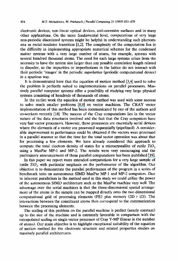
EISEVIER Parallel Computing 21(1995) 853-870 PARALLEL COMPUTING Practical aspects and experiences Perfect scaling of the electronic structure problem on a SIMD architecture Marek T. Michalewicz a,*, Mark Priebatsch b a Division of Information Technology, Commonwealth Scientific ana’ Industrial Research Organization, 723 Swanston Street Carlton, Victoria 3053, Australia b MasPar Computer Corporation, Sydney, Australia; present address: Silicon Graphics, 446 Victoria Road, Gladesville, NS W 211I, Australia Received 4 March 1994;revised 2 November 1994 Abstract We report on benchmark tests of computations of the total electronic density of states of a micro-crystallite of rutile TiO, on MasPar MP-1 and MasPar MP-2 autonomous SIMD computers. The 3D spatial arrangement of atoms corresponds to the two dimensional computational grid of processing elements (PE) plus memory (2D + 1D) while the interac- tions between the constituent atoms correspond to the communication between the PEs. The largest sample we study consists of 491,520 atoms and its size is 41.5 X 41.5 X 1Snm. Mathematically, the problem is equzuknt to solving an n X n eigenvalue problem, where n N 2,5OO,UOO. The program is scalable in the number of atoms, so that the time required to run it is nearly independent of the size of the system in x and y directions (2D PE mesh) and is step-wise linear in z direction (memory axis). The total CPU time for the largest sample on a MasPar MP-2 computer with 16,384 processing elements is m 2.1 hour. Keyworak SIMD, Electronic structure; Benchmark; MasPar 1. Introduction The determination of the electronic structure of systems such as disordered transition metal oxides, amorphous semiconductors or liquid metals is an impor- tant and complex computational problem. It is hoped that the results of such computations will prove immensely valuable in designing new materials for use in * Corresponding author. Email: [email protected] 0167-8191/95/$09.50 0 1995 Elsevier Science B.V. All rights reserved SSDI 0167-8191(94)00097-2
-
Upload
independent -
Category
Documents
-
view
1 -
download
0
Transcript of Perfect Scaling of the Electronic Structure Problem on a SIMD Architecture
EISEVIER Parallel Computing 21(1995) 853-870
PARALLEL COMPUTING
Practical aspects and experiences
Perfect scaling of the electronic structure problem on a SIMD architecture
Marek T. Michalewicz a, * , Mark Priebatsch b
a Division of Information Technology, Commonwealth Scientific ana’ Industrial Research Organization, 723 Swanston Street Carlton, Victoria 3053, Australia
b MasPar Computer Corporation, Sydney, Australia; present address: Silicon Graphics, 446 Victoria Road, Gladesville, NS W 211 I, Australia
Received 4 March 1994; revised 2 November 1994
Abstract
We report on benchmark tests of computations of the total electronic density of states of a micro-crystallite of rutile TiO, on MasPar MP-1 and MasPar MP-2 autonomous SIMD computers. The 3D spatial arrangement of atoms corresponds to the two dimensional computational grid of processing elements (PE) plus memory (2D + 1D) while the interac- tions between the constituent atoms correspond to the communication between the PEs. The largest sample we study consists of 491,520 atoms and its size is 41.5 X 41.5 X 1Snm. Mathematically, the problem is equzuknt to solving an n X n eigenvalue problem, where n N 2,5OO,UOO. The program is scalable in the number of atoms, so that the time required to run it is nearly independent of the size of the system in x and y directions (2D PE mesh) and is step-wise linear in z direction (memory axis). The total CPU time for the largest sample on a MasPar MP-2 computer with 16,384 processing elements is m 2.1 hour.
Keyworak SIMD, Electronic structure; Benchmark; MasPar
1. Introduction
The determination of the electronic structure of systems such as disordered transition metal oxides, amorphous semiconductors or liquid metals is an impor- tant and complex computational problem. It is hoped that the results of such computations will prove immensely valuable in designing new materials for use in
* Corresponding author. Email: [email protected]
0167-8191/95/$09.50 0 1995 Elsevier Science B.V. All rights reserved SSDI 0167-8191(94)00097-2
854 M. T. Michalewicz, M. Priebatsch /Parallel Computing 21 (1995) 853-870
electronic devices, non-linear optical devices, anti-corrosive surfaces and in many other applications. On the more fundamental level, computations of very large non-periodic disordered systems might be helpful in understanding such phenom- ena as metal-insulator transition [1,2]. The complexity of the computation lies in the difficulty in implementing appropriate numerical schemes for the condensed matter systems with a very large number of atoms, for example, systems with several hundred thousand atoms. The need for such large systems arises from the necessity to have the system size larger than any possible correlation length related to disorder, so the impurities or imperfections in the lattice do not interact with their periodic ‘images’ in the periodic superlattice (periodic computational device) in a spurious way.
It is demonstrated here that the equation of motion method [3,4] used to solve the problem is perfectly suited to implementations on parallel processors. Mas- sively parallel computer systems offer a possibility of studying very large physical systems consisting of hundreds of thousands of atoms.
In the earlier work the equation of motion method was used with some success to solve much smaller problems [8,9] on vector machines. The CRAY vector implementation of this method has been communicated by one of the authors and co-workers recently [181. The success of the Cray computations lies in the vector nature of the data structures involved and the fact that the Cray computers have very fast vector processors. However, these processors are essentially serial devices where the elements of a vector are processed sequentially (pipelined). A consider- able improvement in performance could be obtained if the vectors were processed in a parallel manner so that the time for the total vector operation was about that for processing a few elements. We have already considered this approach to compute the total electron density of states for a microcrystallite of r-utile TiO,
using a MasPar MP-1 and MP-2. The results were very encouraging and the preliminary announcement of these parallel computations has been published [19].
In this paper we report more extended computations for a very large sample of rutile TiO, with particular emphasis on the performance of the algorithm. Our objective is to demonstrate the parallel performance of the program in a series of benchmark tests on autonomous SIMD MasPar MP-1 and MP-2 computers. Due to inherent parallelism in the method used in this study we could utilize the power of the autonomous SIMD architecture such as the MasPar machine very well. The advantage over the serial machines is that the three-dimensional spatial arrange- ment of the atoms in the sample can be mapped directly onto the two dimensional computational grid of processing elements (PE) plus memory (2D + ID). The interactions between the constituent atoms then correspond to the communication between the processing elements.
The scaling of this problem on the parallel machine is perfect (nearly constant) up to the size of the machine and is extremely favorable in comparison with the extrapolated scaling on single vector processor of Cray Y-MP (linear in the number of atoms). Our main objective is to highlight exceptional suitability of the equation of motion method for the electronic structure and related properties studies on massively parallel architectures.

M.T. Michalewicz, M. Priebatsch /Parallel Computing 21 (1995) 853-870 855
We need to stress that the computation of properties of the samples with disorder was outside of the scope of this report. However, our studies indicate that the scaling will be very similar (i.e. constant) for point defects and extended surface defects. The point defects will be described by different diagonal matrix elements, which are assigned in one of the preliminary subroutines - this does not influence the running time at all, but the screened electrostatic interaction of the ions with the vacancy will modify the diagonal elements. This modification of diagonal matrix elements was implemented in our program, but is not shown in presented results. The vacancy model we use is given by a Yukawa potential with a soft core [9], and is exponentially decreasing function of inter-ionic distance. Hence only limited number of neighbour sites (PE’s) will be affected by presence of a vacancy The extended surface defects are taken care of by the software masks which ‘switch off atoms from the sample. This does not affect the running time either. We will report on the computations of properties of disordered samples and samples with surface corrugations in a separate communication.
We identify the equation of motion algorithm as one belonging to the class of ‘embarrassingly parallel’ algorithms. The problem it solves is one of the ‘Grand Challenge’ problems.
The paper is organized in the following way: The next section summarizes the physics and the mathematical model underlying the equation of motion method. Next, we describe the SIMD architecture of the MasPar computer, with special emphasis on the communication and the locality of the data. In Section 4 we describe the fine grain parallelism which was implemented in our program and demonstrate the mapping between the atoms and processing elements of the computational mesh. Finally in Section 5 we present the results of parallel performance test runs for different sub-meshes of the PE array, different number of memory layers and FFT steps. We close the paper with conclusions and suggestions for further extension of this work.
2. Electronic structure of disordered systems: mathematical model
2.1 Primer
In solving the purely electronic problem in condensed matter state, physicists often resort to the Born-Oppenheimer model, which treats the atomic cores as the entities fixed in space, so their degrees of freedom do not contribute to the expression for the energy of the outer shell electrons. The energy in quantum mechanics description is expressed by the Hamiltonian operator which takes into account all important contributions arising from the dynamics of outer shell electrons. The Hamiltonian operator acts on the states of the system represented formally by the vectors spanning the Hilbert space. The eigen-values of the Hamiltonian give the allowed energies of the physical system, i.e. in this case the electronic levels in a disordered solid. The group of materials we are interested in such as insulators or semiconductors are reasonably well described by a model
856 M. T. Michalewicz, M. Priebatsch /Parallel Computing 21 (1995) 853-870
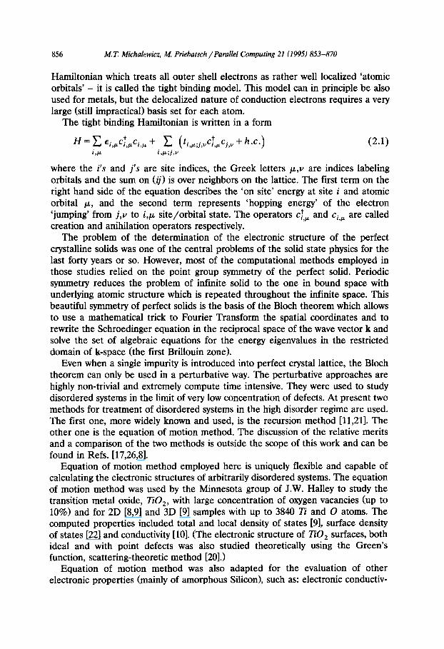
Hamiltonian which treats all outer shell electrons as rather well localized ‘atomic orbitals’ - it is called the tight binding model. This model can in principle be also used for metals, but the delocalized nature of conduction electrons requires a very large (still impractical) basis set for each atom.
The tight binding Hamiltonian is written in a form
lfZ = C Ei,p.Ci,pci,fi + C ( 'i,g;j,vCf,gcj,v + h.c*) (2.1) i9l.L I,cL;J,Y
where the i’s and i’s are site indices, the Greek letters P,V are indices labeling orbitals and the sum on (ij> is over neighbors on the lattice. The first term on the right hand side of the equation describes the ‘on site’ energy at site i and atomic orbital p, and the second term represents ‘hopping energy’ of the electron ‘jumping’ from i,v to i,p site/orbital state. The operators ~1,~ and ci,+ are called creation and anihilation operators respectively.
The problem of the determination of the electronic structure of the perfect crystalline solids was one of the central problems of the solid state physics for the last forty years or so. However, most of the computational methods employed in those studies relied on the point group symmetry of the perfect solid. Periodic symmetry reduces the problem of infinite solid to the one in bound space with underlying atomic structure which is repeated throughout the infinite space. This beautiful symmetry of perfect solids is the basis of the Bloch theorem which allows to use a mathematical trick to Fourier Transform the spatial coordinates and to rewrite the Schroedinger equation in the reciprocal space of the wave vector k and solve the set of algebraic equations for the energy eigenvalues in the restricted domain of k-space (the first Brillouin zone).
Even when a single impurity is introduced into perfect crystal lattice, the Bloch theorem can only be used in a perturbative way. The perturbative approaches are highly non-trivial and extremely compute time intensive. They were used to study disordered systems in the limit of very low concentration of defects. At present two methods for treatment of disordered systems in the high disorder regime are used. The first one, more widely known and used, is the recursion method [11,211. The other one is the equation of motion method. The discussion of the relative merits and a comparison of the two methods is outside the scope of this work and can be found in Refs. [17,26,8].
Equation of motion method employed here is uniquely flexible and capable of calculating the electronic structures of arbitrarily disordered systems. The equation of motion method was used by the Minnesota group of J.W. Halley to study the transition metal oxide, TiO,, with large concentration of oxygen vacancies (up to 10%) and for 2D [8,9] and 3D [9] samples with up to 3840 Ti and 0 atoms. The computed properties included total and local density of states [91, surface density of states [22] and conductivity [lo]. (The electronic structure of TiO, surfaces, both ideal and with point defects was also studied theoretically using the Green’s function, scattering-theoretic method [201.)
Equation of motion method was also adapted for the evaluation of other electronic properties (mainly of amorphous Silicon), such as: electronic conductiv-
M. i? Michakwicz, M. Priebatsch /Parallel Computing 21 (1995) 853-870 857
ity via Kubo formula [161, localization [251, spectral functions 1121, interband linear [27] and non-linear [28] optical properties, electronic structure and conductivity [13], the Hall coefficient 1141, the electronic structure of hydrogenated a-Si [151 and the effective mass of electron and hole in amorphous silicon [29].
2.2. Equation of motion method
The equation of motion method is intuitively very simple. All computations are performed in the direct space. The method effectively computes all the eigenvalues of a sparse square matrix (Schroedinger equation) without resorting to a direct diagonalization. It was shown that this method is well suited for disordered systems with impurities with long range impurity potential [23].
The equation of motion method for the system with many orbitals per site was described in detail in [9,18]. We refer to these papers. In this section we briefly summarize important formal results which form the basis of equation of motion method.
The density of states N,(w) associated with the orbitals of type p is given by:
N,(w)=CCI(nli,~)l’S(o-~~) (2.2) n i
where (n I are the eigenstates of the tight-binding problem in the (disordered) lattice and the I i,p) is the tight-binding state localized on site i and of the orbital
type k It can be shown that the above expression can be represented as
NJ 0) = - iIrn[ /c e-‘~i+&( t )ei’“‘dt ] i
(2.3)
where I;&) = ~,vaj,vGi,p;j,v(t) is the amplitude of Green’s function.
We define the Green’s function in a standard way: Gi,g;j,v(t) = -i@(t)({ci,,(t), c~,(O)l). The time evolution of the quantum system is governed by the equation of motion
ihaFi,Jat = C Hi,p;j,v$i,v (2.4)
j,r
with the initial condition FJO) = -iai,p Physical systems such as insulators or wide gap semiconductors can be described
by the tight binding Hamiltonian, Eq. (2.1). In order to compute the total electronic density of states (for the orbital of type
CL) we set for the coefficients in expression for Fi,p to be: ai,+ = e’“i*c; with random 4i,fi; O < 4i,, ’ 2r*
The connection of physics and massively parallel architecture is contained in Eq. (2.4) and especially Eq. (2.1). The values of hopping integrals ti,p;j,v are communicated between the neighbouring PEs. More details can be found in [8,9,18,191.
858 M. T. Michalewicz, M. Priebatsch /Parallel Computing 21 (I 995) 853-870
3. MasPar autonomous SIMD architecture
MasPar Computer Corporation has designed and implemented a high perfor- mance massively parallel computing system, based on the autonomous SIMD (Single Instruction Multiple Data) paradigm. This is the base system that ran the computations described in this paper. We describe the hardware, the code and architecture usage in some detail below.
The MasPar MP-1 and MP-2 are autonomous SIMD systems. They consist of an Array Control Unit, Processor Array, processor elements, processor memory, X-Net Mesh, Multistage Crossbar Interconnect, an I/O subsystem and a UNIX front end. The Array Control Unit fetches and decodes MP-l/MP-2 instructions, computes addresses and scalar data values, issues control signals to the Processing Element (PE) Array and monitors the PE Array’s status. The Processor Array contains 1024 to 16384 processing elements with associated memory ranging from 16Mbytes to 1Gbyte. Each processing element has an associated local memory ranging from 16Kbytes to 64Kbytes. The processing elements are interconnected via the X-Net Mesh and the Global Router. The X-Net interconnect directly connects each PE with its 8 nearest neighbours in a two-dimensional mesh. The aggregate X-Net communication rate in a 16K PE system exceeds 20 gigabytes per second. The global router allows any PE to communicate with any other PE in the Processor Array. A 16K PE system has an aggregate router communication bandwidth in excess of 1.3 gigabytes per second. The full description of the MasPar architecture can be obtained from references [5,6].
The basic concept for getting the best performance out of these types of systems is to keep as high a percentage as possible of the processing elements (PEs) active for as high a percentage of the runtime as possible. This was achieved by the type of data layout and computational model used. The model allowed for discrete data to be kept on each PE, use of the X-Net only for communications and the duplication of the computation on each PE. This model was ideal for the MasPar architecture, as the only bounding factor for performance and size of the problem was directly related to number of processing elements. The number of processing elements govern available memory for storing the atoms and associated array of neighbourhood interactions as well as the total compute power of the system.
The complexity of the implementation was made simple by the computational model that was designed. In this model each PE contains N, layers of TiO, and an array of interaction values (off-diagonal Hamiltonian matrix elements). The com- putation on each PE is the same, so that for every clock cycle the same instruction on each PE is executed, hence there are no inactive PEs and thus the utilisation percentage during the majority of the computation can be thought of as being close to 100%. Because the size of the problem directly depends on the size of the computing system, that is the number of processing elements and the amount of memory with each PE, the code was benchmarked on systems ranging from an MPllOlD (1K PE 64K memory MP-1) through to an MP2216 (16K PE 64K memory MP-2) for the same number of atoms of r-utile TiO, (iVPE per PE). The benchmarks were run for different number of layers (N,) in memory. Initially N,
M. T. Michalewicz, M. Priebatsch /Parallel Computing 21 (1995) 853-870 859
was set to N, = 2 and was increased in steps of 2 until on a 16K 64K/PE MasPar system the maximum number of layers implemented before memory was exhausted was N, = 10. Hence the maximum size of the rutile sample that could be computed was (N& x N,,,, X N,) = 12g2 X 3 X 10 = 491,520. NMp is the maximum size of MasPar computational array of PEs in one dimension. This total number could be easily increased using the same methodology with more memory per processor, though the time for computation would increase linearly given constant memory access speeds over larger memory. Needless to say computation time would decrease with faster processors or more processors or a combination of larger memory faster processors and/or a larger number of processors.
The good performance achieved was also aided by the fact that communications between processing elements were kept to a minimum by implementing ‘neighbourhood interaction arrays’ (arrays that held common data and information about the interaction between the particular atom and the neighbour atom on the nearest and the second nearest neighbour PEs), and by using only the X-net for PE to PE communications. The drawback, in memory usage and thus lower number of atoms in total that could be modeled, of duplicating an array on every PE instead of using the X-net to pass the data around, or the ACU to broadcast a common data item, was evaluated as being inconsequential compared to the amount of communications that would have been necessary to provide each PE with the correct information as and when required, and the performance hit that this would have caused.
4. Parallel implementation
On massively parallel computers the local environment of each particular processing element and its communication topology defines the physical neigh- bourhood of each atom. We used this fact in coding the interactions between the neighbouring atoms, expressed by the sum over (i,j) in Eq. (2.1). In the vector CRAY version of the program a list of neighbours interacting with each atom was maintained in a look-up table [18]. This introduced a restriction on the vectoriza- tion of the program, although on the CRAY computers it was vectorized using the vectorizing gather-scatter operations. In programming terms, instead of look-up tables used in CRAY vector version of our program [19], we use appropriately defined CSHIFT operations in Fortran90. The computation of the time evolution expressed by Eq. (2.2) is the most time consuming, taking nearly 88% of the total CPU time of the vector version of the program.
Rutile structure of TiO, poses some interesting problems for the mapping of atoms on PE array. The model of the rutile tight-binding Hamiltonian we use in our study, originally proposed by Vos [24] is non-trivial. It is characterized by the following features: 6) the sample is three dimensional; (ii) the rutile structure consists of tetragonal unit cell with two Ti and four 0
atoms. The titanium atoms occupy the positions (O,O,O) and (3, i, 3) whereas
860 M.T. Michalewicz, M. Priebatsch /Parallel Computing 21 (1995) 853-870
L_ oxygens are at the positions f (x, x, 0), and f ($ + x, 2 x, $), where
x = 0.306 f 0.001 [7]. Each Ti cation forms a ‘dumbell’ shape with two
neighbouring 0 anions. The ‘dumbell’ attached to the Ti in the centre of the unit cell is rotated by 90” with respect to the eight ‘dumbells’ attached to the Ti atoms at the corners of the unit cell. This rotation complicates the mapping somewhat;
(iii) there are up to five atomic orbitals at each atom, i.e. five 3d orbitals for each Ti and one 2s and three 2p orbitals for each 0 atom;
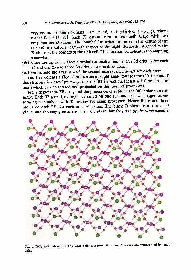
(iv) we include the nearest and the second-nearest neighbours for each atom. Fig. 1 represents a slice of t-utile seen at slight angle towards the (001) plane. If
this structure is viewed precisely from the [OOl] direction, then it will form a square mesh which can be rotated and projected on the mesh of processors.
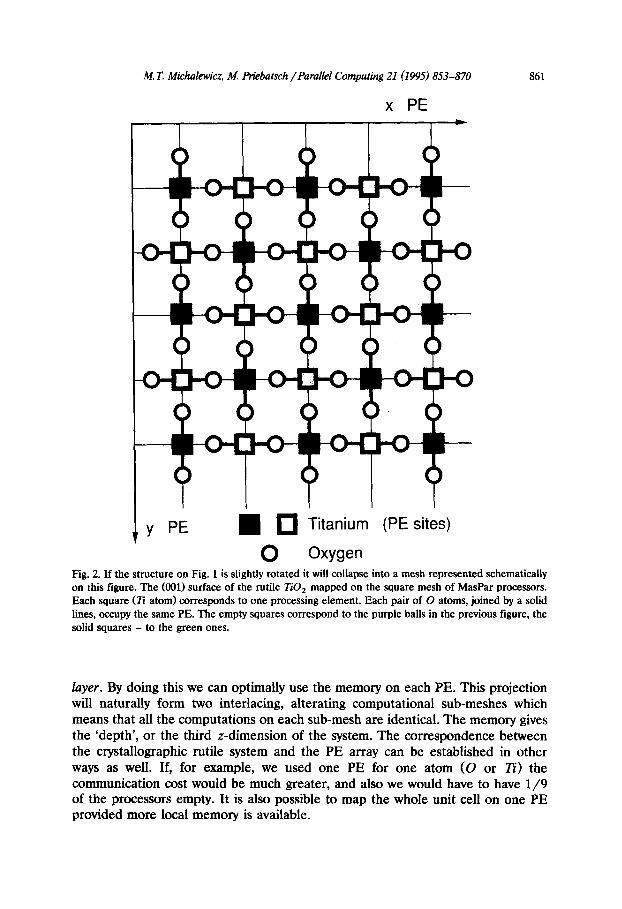
Fig. 2 depicts the PE array and the projection of t-utile in the (001) plane on this array. Each Ti atom (square) is centered on one PE, and the two oxygen atoms forming a ‘dumbell’ with Ti occupy the same processor. Hence there are three atoms on each PE, for each unit cell plane. The black Ti sites are in the z = 0 plane, and the empty ones are in z = 0.5 plane, but they occupy the same memory
Fig. 1. Tio2 rutile structure. The large balls represent Ti atoms, . 0 atoms are represented by small
balls.
M. T. Michalewicz, M. Priebatsch /Parallel Computing 21 (1995) 853-870
x PE
Y PE n o Titanium (PE sites)
0 Oxygen Fig. 2. If the structure on Fig. 1 is slightly rotated it will collapse into a mesh represented schematically on this figure. The (001) surface of the rutile TiU, mapped on the square mesh of MasPar processors. Each square (Ti atom) corresponds to one processing element. Each pair of 0 atoms, joined by a solid lines, occupy the same PE. The empty squares correspond to the purple balls in the previous figure, the solid squares - to the green ones.
layer. By doing this we can optimally use the memory on each PE. This projection will naturally form two interlacing, alterating computational sub-meshes which means that all the computations on each sub-mesh are identical. The memory gives the ‘depth’, or the third z-dimension of the system. The correspondence between the crystallographic rutile system and the PE array can be established in other ways as well. If, for example, we used one PE for one atom (0 or Ti) the communication cost would be much greater, and also we would have to have l/9 of the processors empty. It is also possible to map the whole unit cell on one PE provided more local memory is available.
862 M.T. Michalewicz, M. Priebatsch /Parallel Computing 21 (1995) 853-870
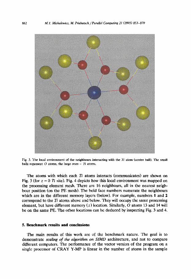
Fig. 3. The local environment of the neighbours interacting with the Ti atom (center ball). The small balls represent 0 atoms, the large ones - Ti atoms.
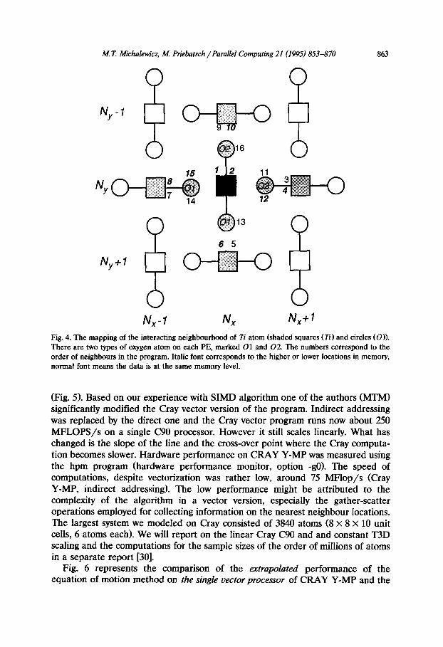
The atoms with which each Ti atoms interacts (communicates) are shown on Fig. 3 (for z = 0 Ti site). Fig. 4 depicts how this local environment was mapped on the processing element mesh. There are 16 neighbours, all in the nearest neigh- bour position (on the PE mesh). The bold face numbers numerate the neighbours which are in the different memory layers (below). For example, numbers 1 and 2 correspond to the Ti atoms above and below. They will occupy the same processing element, but have different memory (z> location. Similarly, 0 atoms 13 and 14 will be on the same PE. The other locations can be deduced by inspecting Fig. 3 and 4.
5. Benchmark results and conclusions
The main results of this work are of the benchmark nature. The goal is to demonstrate scaling of the algotithm on SIMD architecture, and not to compare different computers. The performance of the vector version of the program on a single processor of CRAY Y-MP is linear in the number of atoms in the sample
M. T. Michalewicz, M. Priebatsch /Parallel Computing 21 (1995) 853-870 863
NY+1
Nx N,+l Fig. 4. The mapping of the interacting neighbourhood of Tz’ atom (shaded squares (Ti) and circles (0)). There are two types of oxygen atom on each PE, marked 01 and 02. The numbers correspond to the order of neighbours in the program. Italic font corresponds to the higher or lower locations in memory, normal font means the data is at the same memory level.
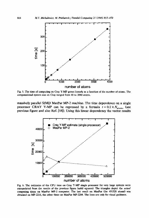
(Fig. 5). Based on our experience with SIMD algorithm one of the authors (MTM) significantly modified the Cray vector version of the program. Indirect addressing was replaced by the direct one and the Cray vector program runs now about 250 MFLOPS/s on a single C90 processor. However it still scales linearly. What has changed is the slope of the line and the cross-over point where the Cray cornputa- tion becomes slower. Hardware performance on CRAY Y-MP was measured using the hpm program (hardware performance monitor, option -go). The speed of computations, despite vectorization was rather low, around 75 MFlop/s (Cray Y-MP, indirect addressing). The low performance might be attributed to the complexity of the algorithm in a vector version, especially the gather-scatter operations employed for collecting information on the nearest neighbour locations. The largest system we modeled on Cray consisted of 3840 atoms (8 x 8 x 10 unit cells, 6 atoms each). We will report on the linear Cray C90 and and constant T3D scaling and the computations for the sample sizes of the order of millions of atoms in a separate report [30].
Fig. 6 represents the comparison of the extrapolated performance of the equation of motion method on the singZe vector processor of CRAY Y-MP and the
864 M. T. Michalewicz, M. Priebatsch /Parallel Computing 21 (1995) 853-870
number of atoms Fig. 5. The time of computing on Cray Y-MP grows linearly as a function of the number of atoms. The computational system size on Cray ranged from 48 to 3840 atoms.
massively parallel SIMD MasPar MP-2 machine. The time dependence on a single processor CRAY Y-MP can be expressed by a formula t = 0.1 x N,,,,, (see previous figure and also Ref. [18]). Using this linear dependency the vector results
40~o~ * Cray Y-MP estimate (single processor) J
.,.. A
I I I I I J
0 1oOooo 2ooooo 3ooooo 400000 5ooooo
number of atoms Fig. 6. The estimates of the CPU time on Cray Y-MP single processor for very large systems were extrapolated from the results of the previous figure (solid squares). The triangles depict the actual computing times on MasPar MP-2 computer. The last result on MasPar (for 491520 atoms) was obtained on MP-2216, the other three on MasPar MP-2204. The lines are only for visual guidance.
M. T. Michalavicz, M. Priebatsch /Parallel Computing 21 (1995) 853-870 865
were extrapolated for the samples of up to 491,520 atoms. They are represented as black squares on Fig. 6. The MasPar MP-2 results represented by triangles correspond to actual computations for 32 X 32 X 2, 64 X 64 X 2, 128 X 128 x 2 and 128 X 128 x 10 samples (x,y-mesh of PE array X memory ‘cells’; each holding three atoms). On MasPar computers we used 1Gbyte memory: all local memory on all the processors for the 491,520 atoms run. The size of TiO, sample studied on MasPar machines was up to 128 times bigger than the largest sample studied by us on single processor of CRAY Y-MP vector supercomputer. It would take nearly 14 hours CPU time to compute the electronic density of states for the sample this large on a single processor of CRAY Y-MP. The cross-over point for better parallel performance is reached for the samples of 125,000 atoms. It is seen that the scaling of parallel performance is nearly perfect: the time of computation remains nearly constant (in fact it even drops down) as the sample size grows. The lines are drawn for the eye guidance only. The last two points were computed using newer version of the FORTRAN compiler, hence the apparent appearance of the decreasing time. The last point was obtained on MasPar MP-2216, all others on MasPar MP-2204.
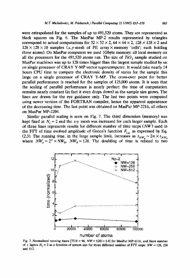
Similar parallel scaling is seen on Fig. 7. The third dimension (memory) was kept fixed at N, = 2 and the x-y mesh was increased for each larger sample. Each of three lines represents results for different number of time steps (NW) used in the FFT of time evolved amplitude of Green’s function Fi,cL as expressed by Eq. (2.3). The running time, in the large sample limit, increases as t,w, N 2n X fNwO
where NW,, = 2” x NW,, NW, = 128. The doubling of time is related to two
I I I 1
12- Nz=2
_ r....~..“.’ .,... AL.. . . . . . . .._.. -.- NW=128
‘.,. .,.,.,_, u NW=256 - 10 ‘,I
.‘...,_ ‘.,. .,.,.,., x NW=512-
5 4 / .,..., Y., %..,
.i? 8- . .‘I.,.,
Y.,.,
-i+ K
E - b 6- c
l I I I I
0 20000 40000 60000 80000 100000
number of atoms Fig. 7. Normalised running times [ T(N = 96, NW = 128) = 1.01 for MasPar MP-1116, and fiied number of z layers N, = 2 as a function of system size for three different number of FFT steps: NW = 128,256 and 512.

866 M. T. Michalewicz, M. Priebatsch /Parallel Computing 21 (199.5) 853-870
Fig. 8. Normalised running time for different slab shapes (with fixed N, = 2) vs. number of FFT steps.
1’1’1 * 1’1’ 1'1.1'
12- 1 - ,,,’
10 - + 4x4x2
-0. 16x16~2 + 32x32~2
N 8- w 64x64~2
.- -a-- 128x128~2
b 6- c
I. I * I I I I 1.1. I. I1 100 150 200 250 300 350 400 450 500 550
FFT steps
computational sub-meshes, and this in turn is related to limited amount of memory on each PE.
The same results are also represented on Fig. 8 in a slightly different way. Here the normalized running time is a function of the number of FFT time steps. Each line represents a physical system of fixed size (computational sub-mesh).
The normalized time as a function of the number of memory layers (N,) is plotted on Fig. 9. The plot indicates that the run-time is a step-wise linear function of the memory layer, i.e. increasing linearly every two layers (corresponding to
MasPar MP-1, NW=51 2, 128xl28xNz
2.5. ? - %- ’
”
z2.0. ,,*’
>’ E /’ ‘s .:’ s1.5.
g b /* /L____/’
‘7 .o . *________****‘-
2 4 N62
8 IO
Fig. 9. Normalised running time vs. number of memory layers N,. The computations were performed on MasPar MP-1116 with NW = 512.
M. T. Michalewicz, M. Priebatsch /Parallel Computing 21 (1995) 853-870 867
t I I I I I
0 5000 10000 15000 20000 25000
number of atoms Fig. 10. Normal&d running time vs. number of atoms for MP-1116 and MP-2216 MasPar computers. The number of memory layers was kept fuced at N, = 10 and the FFT was taken for NW= 512.
‘thickness’ of the sample in z dimension or c crystallographic axis). We would have to run the program for samples with N, > 10 to confirm such scaling. At present we can not run such tests due to limited local memory on each PE.
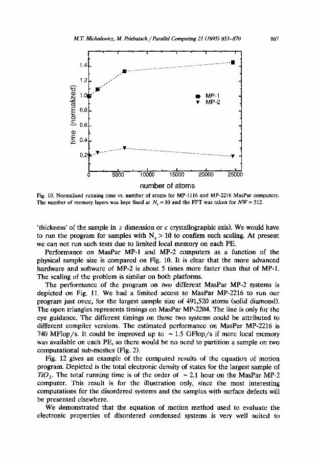
Performance on MasPar MP-1 and MP-2 computers as a function of the physical sample size is compared on Fig. 10. It is clear that the more advanced hardware and software of MP-2 is about 5 times more faster than that of MP-1. The scaling of the problem is similar on both platforms.
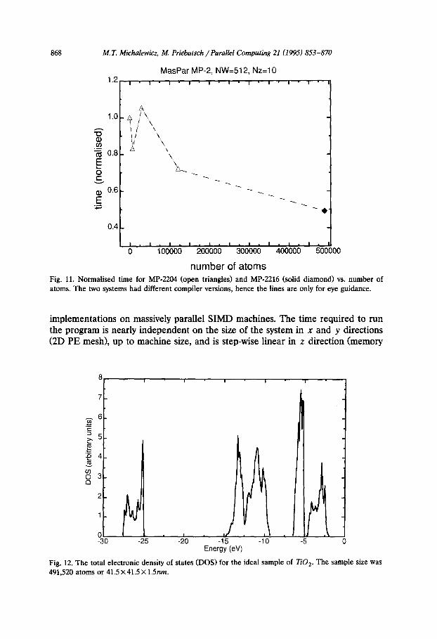
The performance of the program on &vo different MasPar MP-2 systems is depicted on Fig. 11. We had a limited access to MasPar MP-2216 to run our program just once, for the largest sample size of 491,520 atoms (solid diamond). The open triangles represents timings on MasPar MP-2204. The line is only for the eye guidance. The different timings on those two systems could be attributed to different compiler versions. The estimated performance on MasPar MP-2216 is 740 MFlop/s. It could be improved up to N 1.5 GFlop/s if more local memory was available on each PE, so there would be no need to partition a sample on two computational sub-meshes (Fig. 2).
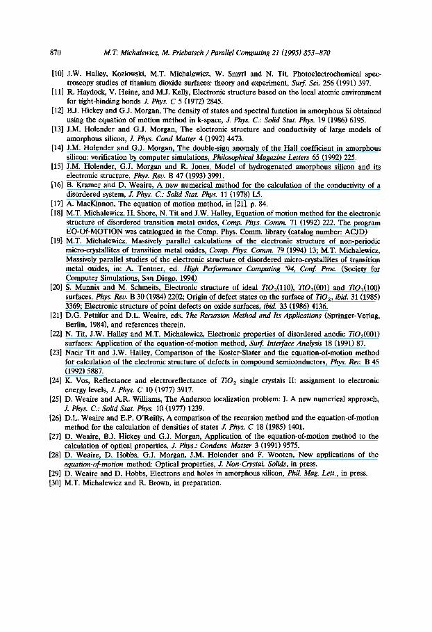
Fig. 12 gives an example of the computed results of the equation of motion program. Depicted is the total electronic density of states for the largest sample of TiO,. The total running time is of the order of N 2.1 hour on the MasPar MP-2 computer. This result is for the illustration only, since the most interesting computations for the disordered systems and the samples with surface defects will be presented elsewhere.
We demonstrated that the equation of motion method used to evaluate the electronic properties of disordered condensed systems is very well suited to
868 M. T. Micbalewicz, M. Priebatsch /Parallel Computing 21 (1995) 853-870
MasPar MP-2, NW=51 2, Nz=lO 1.2 , . , . , . , . , , , . , . , . , . , , c
0.4 -
I. I .I .,., .I .I .I. I .I, I 0 100000 200000 300000 400000 500000
number of atoms Fig. 11. Normalised time for MP-2204 (open triangles) and MP-2216 (solid diamond) vs. number of atoms. The two systems had different compiler versions, hence the lines are only for eye guidance.
implementations on massively parallel SIMD machines. The time required to run the program is nearly independent on the size of the system in x and y directions (2D PE mesh), up to machine size, and is step-wise linear in t direction (memory
a
-20 -15 -10 Energy (eV)
Fig. 12. The total electronic density of states (DOS) for the ideal sample of TiOl. The sample size was 491,520 atoms or 41.5 x41.5X 1.5nm.

M. T MichaLwicz, M. Priebatsch /Parallel Computing 21 (1995) 853-870 869
axis). The program described in this paper can be used to compute the electronic properties for the samples with cleaved surfaces of different Miller indices, modeling the shape of the microcrystallite in a stone-cutter fashion. The extended surface defects and fabricated features such as stepped surfaces, superlattices, modulated superlattices or doped samples can now be investigated by methods described here. All these features can be programmed as software masks which switch-off atoms (PEs) outside the bounds of a sample. We are now working towards applying methods described here to computations of the linear and non-linear transport properties in disordered systems and implementing the pro- gram on MIMD T3D massively parallel Cray system.
Acknowledgments
MTM wishes to thank Dr. I.D. Mathieson, P.G. Whiting, S. McClenahan and S. Pickering for discussions and hints on parallel programming. The program de- scribed in this paper was developed on the MasPar MP-1 computer at the Ormond Supercomputer Facility which is a joint facility of The University of Melbourne and The Royal Melbourne Institute of Technology and on the MasPar MP-2204 at Monash University, Melbourne. The CRAY part of this project was computed on CSIRO Supercomputing Facility CRAY Y-MP4/364 (at the time of writing Y-MP4/464) in Melbourne. I am very grateful to Kelly Pickard from MasPar Corporation for running my program on MasPar MP-2216 in Sunnyvale. I wish to thank Dr Anneliese Palmer of Biosym Technologies, Inc., Sydney, for her help in producing Fig. 1 and 4 using Biosym Technologies’ Solids Builder and Solids Adjuster.
References
[l] N.F. Mott, Metal-Znsulator Transitions (Taylor & Francis, London, 1990). [2] J.M. Holender and G.J. Morgan, Electron localization in models of hydrogenated amorphous
silicon and pure amorphous silicon, Moa’elling and Simulation in Mat. Sci. and Eng. 2 (1) (1994). [3] R. Alben, M. Blume, H. Krakauer and L. Schwartz, Exact results for a three-dimensional alloy
with site diagonal disorder: comparison with the coherent potential approximation, Phys. Reu. B 12, (1975) 4090.
[4] D. Beeman and R. Alben, Vibrational properties of elemental amorphous semiconductors, Advances in Phys. 26 (1977) 339.
[5] T. Blank, The MasPar MP-1 architecture, in: IEEE Computer Society Press Reprint - Spring COMPCON 90.
161 The design of the MasPar MP-2: A cost effective massively parallel computer, MasPar Computer Corporation.
[7] F.A. Grant, Properties of rutile (titanium dioxide), Reu. Mod. Phys. 31 (1959) 646. [8] J.W. Halley and H. Shore, Equation-of-motion method for the study of defects in insulators:
Application to a simple model of TiO, Phys. Reu. B 36 (1987) 6640. [9] J.W. Halley, M.T. Michalewicz and N. Tit, Electronic structure of multiple vacancies in rutile DO,
by the equation-of-motion method, Phys. Reu. B 41 (1990) 10165.
870 M. T Michalewicz, M. Priebatsch /Parallel Computing 21 (1995) 853-870
[lo] J.W. Halley, Kozlowski, M.T. Michalewicz, W. Smyrl and N. Tit, Photoelectrochemical spec- troscopy studies of titanium dioxide surfaces: theory and experiment, Surf: Sci. 256 (1991) 397.
[ll] R. Haydock, V. Heine, and M.J. Kelly, Electronic structure based on the local atomic environment for tight-binding bonds J. Phys. C 5 (1972) 2845.
[12] B.J. Hickey and G.J. Morgan, The density of states and spectral function in amorphous Si obtained using the equation of motion method in k-space, J. Phys. C.: Solid Stat. Phys. 19 (1986) 6195.
[13] J.M. Holender and G.J. Morgan, The electronic structure and conductivity of large models of amorphous silicon, J. Phys. Cond Matter 4 (1992) 4473.
[14] J.M. Holender and G.J. Morgan, The double-sign anomaly of the Hall coefficient in amorphous silicon: verification by computer simulations, Philosophical Magazine Letters 65 (1992) 225.
[15] J.M. Holender, G.J. Morgan and R. Jones, Model of hydrogenated amorphous silicon and its electronic structure, Phys. Rev. B 47 (1993) 3991.
[16] B. Kramer and D. Weaire, A new numerical method for the calculation of the conductivity of a disordered system, J. Phys. C.: Solid Stat. Phys. 11 (1978) L5.
[17] A. MacKinnon, The equation of motion method, in [21], p. 84. [18] M.T. Michalewicz, H. Shore, N. Tit and J.W. Halley, Equation of motion method for the electronic
structure of disordered transition metal oxides, Comp. Phys. Comm. 71 (1992) 222. The program EQ-Of-MOTION was catalogued in the Comp. Phys. Comm. library (catalog number: ACJD)
[19] M.T. Michalewicz, Massively parallel calculations of the electronic structure of non-periodic micro-crystallites of transition metal oxides, Comp. Phys. Comm. 79 (1994) 13; M.T. Michalewicz, Massively parallel studies of the electronic structure of disordered micro-ctystallites of transition metal oxides, in: A. Tentner, ed. High Performance Computing ‘94, Conf Proc. (Society for Computer Simulations, San Diego, 1994)
[20] S. Munnix and M. Schmeits, Electronic structure of ideal 7X&(110), TiO,(OOl) and TiO,(lOO) surfaces, Phys. Rev. B 30 (1984) 2202; Origin of defect states on the surface of TiO,, ibid. 31(1985) 3369; Electronic structure of point defects on oxide surfaces, ibid. 33 (1986) 4136.
[21] D.G. Pettifor and D.L. Weaire, eds. The Recursion Method and Its Applications (Springer-Verlag, Berlin, 1984), and references therein.
[22] N. Tit, J.W. Halley and M.T. Michalewicz, Electronic properties of disordered anodic TiO,(OOl) surfaces: Application of the equation-of-motion method, Surf. Interface Analysis 18 (1991) 87.
[23] Nacir Tit and J.W. Halley, Comparison of the Koster-Slater and the equation-of-motion method for calculation of the electronic structure of defects in compound semiconductors, Phys. Rev. B 45 (1992) 5887.
[24] K. Vos, Reflectance and electroreflectance of TiOz single crystals II: assignment to electronic energy levels, J. Phys. C 10 (1977) 3917.
[25] D. Weaire and A.R. Williams, The Anderson localization problem: I. A new numerical approach, .I. Phys. C.: Solid Stat. Phys. 10 (1977) 1239.
[26] D.L. Weaire and E.P. O’Reilly, A comparison of the recursion method and the equation-of-motion method for the calculation of densities of states J. Phys. C 18 (1985) 1401.
[27] D. Weaire, B.J. Hickey and G.J. Morgan, Application of the equation-of-motion method to the calculation of optical properties, J. Phys.: Condens. Matter 3 (1991) 9575.
[28] D. Weaire, D. Hobbs, G.J. Morgan, J.M. Holender and F. Wooten, New applications of the equation-of-motion method: Optical properties, J. Non-Crystal. Solids, in press.
[29] D. Weaire and D. Hobbs, Electrons and holes in amorphous silicon, Phil. Mag. Lett., in press. [30] M.T. Michalewicz and R. Brown, in preparation.