PCB007 Magazine, August 2019
120
AUGUST 2019 I PCB007 MAGAZINE 1
-
Upload
khangminh22 -
Category
Documents
-
view
0 -
download
0
Transcript of PCB007 Magazine, August 2019

AUGUST 2019 I PCB007 MAGAZINE 1
AUGUST 2019
better products through improved chemistry

Registered members of my I-Connect007 have 24/7 access to our ever-growing library of eBooks, which now includes a wide range of topics from DFM to Complex PCBs.
EEnrich your mind and expand your knowledge! Download these popular
titles with just a click.
They’re pretty awesome!
I-007eBooks.com

Your life just got better.
I-007ebooks.com/doc DOWNLOAD NOW
This book will teach you how to save time and money, reduce frustration, and make your job easier!

4 PCB007 MAGAZINE I AUGUST 2019
AUGUST 2019 • FEATURED CONTENT
In this issue, we explore plating, including the chemistries and processes that make up traditional subtractive etch and plate. We also investigate the confluence of smaller dimensions, reduced pollu-tion, higher throughput, and improved reliability as they relate to wet processes and plating. Further, we address some of the emerging processes for higher-performance designs and new equipment to implement modern techniques.
Wet Processes & Plating
The State of Platingby Marc Ladle
Chemcut: Wet Processing Equipment for the Long HaulInterview with Rick Liesand Jerry Reitz Putting Green Into a Brownfield FacilityInterview with George Milad
The Advantages of Non-sludge Acid Copper ProductsInterview with Mike Wood
Pollution Prevention Techniques:Rinse Water Reductionby Peter Moleux with contributions from Happy Holden
10
20
28
36
44
20
10

The only thing constant,is change.
-HeraclitusAt Eternal Technology Corporation, we value disruptive innovation as an answer to change. We believe that those who choose to disrupt and innovate stay relevant; those who don’t, run the risk of becoming obsolete. Staying relevant means staying connected: internally with our employees and partners, externally with our customers, and globally with emerging trends and markets.
PLEASE JOIN US IN WELCOMING OUR STRONGEST PARTNERSHIP TO DATE.
IEC IS NOW OUR SOLE NORTH AMERICAN DISTRIBUTOR!
Eternal Technology Corporation1800 Touchstone RoadColonial Heights, VA 23834 U.S.ATEL: +1-804-524-8555https://[email protected]
International Electronic Components Inc.809 Aldo Avenue, Unit 104
Santa Clara, CA 95054 U.S.A.TEL: +1-855-225-9333
https://[email protected]

6 PCB007 MAGAZINE I AUGUST 2019
SHORTS:Red Wine May Hold the Key to Wearable Electronics
Mobile Performance Report Shows Incredible Speeds on 5G Compared to LTE
New Filter Enhances Robot Vision on 6D Pose Estimation
Cardiff Delivers Compound Semiconductor Breakthrough
Cyborg-like Microchip Valve Driven by Earthworm Muscle
'Seeing' in Real Time
DEPARTMENTS:Career OpportunitiesEvents CalendarAdvertiser Index & Masthead
HIGHLIGHTS:MilAero007 EIN007 Industry News PCB007 SuppliersTop 10 from PCB007
ARTICLES:Innovative Electroplating Processes for IC Substratesby Saminda Dharmarathna, et al.
SAP Utilizing Very Uniform Ultrathin Copperby Steve Iketani and Mike Vinson
Vertical Conductive Structures, Part 3: Design Tool Techniquesby Ed Hickey, Mike Catrambone, andJoan Tourné
Solder Mask Curing: UV Bump Overviewby Nikolaus Schubkegel
COLUMNS:There’s An Art to Platingby Nolan Johnson
CFX and Hermes: The Plug-and-Play IPC Standards Building Momentum for Industry 4.0by Dr. John Mitchell
Via Hole Filling and Plugging, Part 1by Michael Carano
The Past 15 Years: Changes to MIL-PRF-31032 Certification, Part 1by Mike Hill
56
76
90
100
8
16
40
72
9
39
43
55
69
103
107118119
347088104
AUGUST 2019 • ADDITIONAL CONTENT
56

8 PCB007 MAGAZINE I AUGUST 2019
There’s definitely an art to plating. Start with a generally planar substrate, then alternately put stuff on and take things off. Continue this in subtle variations until what you have is the stuff you want, where you want.
There are classes on plating (I’m talking about food now) pretty much everywhere. Es-coffier, arguably the hub of French cuisine, offers an online course, and cooking schools, kitchen equipment retailers, and even com-munity colleges offer training. The San Francisco Cooking School offers an in-person work-shop on plating. In fact, the course description states, “By the end of the class, you will understand why the shape color and size of table-ware is impor-tant when plating food.” Ah-hah! The equipment and tools are as im-portant as the raw materials; it doesn’t matter whether we’re talking food or PCBs.
Years back—at least in my part of the under-refined United States—plating food meant something large, bulky, and robust; that’s how it was in our industry too during that era. But things change, and refinements are made. Even in the Wild West of the U.S., thoughtfully crafted plates with smaller portions appear on tables more often.
There are both differences and similarities when using food plating as a metaphor. As we become more sophisticated in the products we
create, it isn’t enough to run rough chemistries in crude facilities; one cannot deliver the fine details, small geometries, and precision that OEMs now expect from our fabricators worldwide. We can’t be short-order line cooks any longer; we must become chefs of precision.
In this issue, we explore our kind of plat-ing, including the chemistries and processes that make up traditional subtractive etch and
plate. We also investigate the confluence of smaller dimensions, reduced pol-
lution, higher throughput, and improved reliability as they
relate to wet processes and plating. Further,
we address some of the emerging pro-cesses for higher performance de-signs and new equipment to im-plement modern techniques be-cause the high-end techniques of today
become the main-stream techniques of
tomorrow.Marc Ladle makes the
first splash with his fea-ture, “The State Of Plating.”
Dr. John Mitchell follows with his column highlighting “CFX and Hermes:
The Plug-and-Play IPC Standards Building Momentum for Industry 4.0.” Chemcut CEO Rick Lies talks with publisher Barry Matties about “Wet Processing Equipment for the Long Haul.” Then, in “Putting Green Into a Brown-field Facility,” Uyemura’s George Milad talks with me about the challenges and solutions in customizing up-to-date process chemistries
Nolan’s Notesby Nolan Johnson, I-CONNECT007
There’s An Art to Plating

AUGUST 2019 I PCB007 MAGAZINE 9
to fit pre-existing facilities. Wrapping up the features, Cerambus’ Mike Wood discusses “The Advantages of Non-sludge Acid Copper Products.”
Columnist Mike Carano debuts his next se-ries off the starting blocks with “Via Hole Fill-ing and Plugging, Part 1.” Of course, in wet processing, rinsing is a critical step, so Happy Holden’s article addresses “Pollution Preven-tion Techniques: Rinse Water Reduction.” And finally, Saminda Dharmarathna, et al., cover “Innovative Electroplating Processes for IC Substrates: Via, Through-hole, and Embedded Trench Fill.” Mike Hill also debuts Part 1 of his column, “The Past 15 Years—Changes to MIL-PRF-31032 Certification, Part 1.”
Continuing with the technical pieces, Steve Iketani and Mike Vinson post their re-
Nolan Johnson is managing editor of PCB007 Magazine. Nolan brings 30 years of career experience focused almost entirely on electronics de-sign and manufacturing.To contact Johnson, click here.
search on “Semi-additive Process (SAP) Uti-lizing Very Uniform Ultrathin Copper by a Novel Catalyst.” Then, we continue Part 3 of Joan Tourné’s series on vertical conduc-tive structures (VeCS) and design techniques, along with Ed Hickey and Mike Catrambone. Nikolaus Shubkegel makes his return to the magazine with his article, “Solder Mask Cur-ing: UV Bump Overview.”
Now, by all means, load up your plate! PCB007
coffee, or black tea is spilled on a dress, it’s difficult to get rid of these stains. The main reason is that they all contain tannic acid, which can firmly adsorb the material on the surface of the fiber. This good adhesion is exactly what
we need for durable wearable, conductive devices.”
The research was published in the journal Small. The over-all impact of this new method could see a reduction in price for wearable technology, along with improvements in comfort and robustness.
The improved conductivity can allow technology devel-opers to use more comfort-able fabrics, such as cotton, to replace nylon. The technol-ogy can also allow for circuits to be printed directly on to the surface of clothing to make a comfortable, flexible circuit board.
(Source: The University of Manchester)
Extracting tannic acid from red wine, coffee, or black tea led a team of scientists from The University of Manchester to develop much more durable and flexible wearable devices.
Previously, wearable tech-nology has been subject to fail after repeated bending and folding, which can interrupt the conductivity of such devices due to micro-cracks. Improv-ing this could open the door to more long-lasting integrated technology.
“We are using this method to develop new flexible, breath-able, wearable devices. The main research objective of our group is to develop com-fortable wearable devices for flexible human-machine inter-face,” said Dr. Xuqing Liu, who led the research team. “Tradi-tional conductive material suf-fers from weak bonding to the fibers, which can result in low conductivity. When red wine,
Red Wine May Hold the Key to Wearable Electronics

10 PCB007 MAGAZINE I AUGUST 2019
Feature by Marc LadleVIKING TEST LTD.
The current market for selling plating lines for panel and pattern plating circuit boards in Europe is not exactly huge. Since I have been involved in selling this type of equipment, the company I work for has probably averaged the sale of one machine per year. Normally, this has been due to the replacement of complete-ly worn-out equipment or reinstatement of a factory after a fire. Within the last 12 months, we have sold the first line based completely on the requirement for advancing technology. Al-though this sample group is not large enough to see any real trend, I have a feeling that the Eu-ropean PCB industry is likely to see an increas-ing demand for machines that can achieve re-sults to meet the demands of the newest ideas for electronic printed circuit design.
ExamplesWe rarely have a blank canvas to work with.
In nearly every case, we must try to fit a quart in a pint pot. Space is the enemy when it comes to integrating the best available new technol-
ogy into the footprint of the previous 20-year-old plating line. To make matters worse, it is not unusual to be asked to increase the output capacity of the equipment at the same time.
Increasingly, PCB design technology utilises buried and blind via holes and plated via fill is also becoming more and more common. The buried and blind holes mean that the loading on the plating equipment is multiplied by the number of different inner layer connections. The same technology means that equipment needs to deal with thinner and thinner ma-terials. Plating copper via fill typically means the tank design must be larger, so it takes up more of the valuable space available and takes a long time compared to a traditional through-hole cycle. A typical through-hole plate might take 45–60 minutes where a via hole run could be 3–4 hours.
It is well known that the size of PCB facto-ries in Europe is usually much smaller than the factories in Asia. Typically, this means there is only a single plating line available to produc-tion, and this one piece of key equipment must cover every type of work which goes through the factory. Compromises must be made, and

“We are excited to be the first Taiyo Inkjet solder mask customer in North America. The IJSR-4000 JM02DG solves the most challenging solder mask issues of mask in holes, mask on pad and registration.”
— Rich Clemente, General Manager, Lenthor Engineering
“Bringing Inkjet solder mask to the North American market has surpassed our timeline thanks to Lenthor’s partnership.”
— John Fix, Manager & Director, Sales and Marketing, Taiyo America
“In my 34 years in circuit boards I never thought I’d see Inkjet solder mask, way to go Taiyo.”
— Steve Franzino, Senior Process Engineer, Lenthor Engineering
Phone [775] 885-9959 • www.taiyo-america.com • [email protected]
Brian WojtkiewiczTaiyo America
Rich ClementeLenthor Engineering
Steve FranzinoLenthor Engineering
John FixTaiyo America
THE NEXT BIG THING IN SOLDER MASK IS HERE!

12 PCB007 MAGAZINE I AUGUST 2019
usually, it is the work at the extremes of capa-bility that suffer. For example, very thick heavy panels are hard to transport using commonly used top-clamping methods (they can drop out of the clamps unexpectedly). Very thin panels need extra support to stop them folding when they are dipped into the tanks and also to keep them in a stable position in the centre of the tank between the anodes (the plating will be too heavy on the side closer to the anodes and too thin on the side which is further from the anodes). For both problems, simple solutions are available, but the same fix does not suit both extremes at the same time.
The plating chemistry has also advanced when compared to the simple solutions and re-plenishment additives of years ago. Again, the major problem for smaller manufacturers is the sheer amount of variation in the work they have to put down the line and the fast turn arounds required by customers that prevent them from batching similar work together. The chemistry in a bath can definitely be tuned to provide even plating of a large area, such as panel plating where the whole surface of the panel is plated as well as the through-holes, but the same tuning is likely to make it very difficult to plate isolated details or very small plating areas. In the worst case, the additives have to be stripped out of the solution using a carbon filter and then added again to suit the next requirement.
Solutions and DevelopmentsAll of the previous cases are real examples
I have come across during the last year, and they are very big problems for the companies involved. In some cases, the only practical so-lution is a larger factory and a second special-purpose plating line. Development of hardware to meet the needs of the large range of chal-lenges facing the plating operation has recent-ly been quite strong. There are a number of features becoming more commonplace on new equipment and some that could also be retro-fitted to existing equipment.
Zoned anodes are an interesting approach to help overcome distribution issues. Tradi-tional soluble anodes using titanium baskets
filled with copper balls do not lend themselves to being able to control different areas of the plating window. They are typically hung on a single anode bar, and the plating current is ap-plied evenly to the whole anode area. Using insoluble iridium mesh anodes allows zoning of the anode area, and you can control the cur-rent by depth by splitting the anode into sec-tions and only applying the current to the sec-tion of the anode with a panel in front of it. This allows more accurate plating of different panel lengths without having to revert to float-ing shields.
Multiple rectifiers give the capability to split the plating window into sections across its width. This could be used to allow flight bars to run partly loaded with much more pre-dictable results. This approach could be used alongside zoned anodes to provide an almost endless combination of ways to be able to split the plating window to achieve more ac-curate copper plating. Like the zoned anodes, this approach has many possible applications
Figure 1: Zoned anode section.

AUGUST 2019 I PCB007 MAGAZINE 13
Electroplating very thin panels has always been difficult due to the nature of the “dip” process. If you use a conventional plating line, the panel has to be supported by a jig of some type to keep the very flexible panel in the cor-rect position as it is lowered into the plating tank. In comparison, VCP can be formatted with Teflon guides, which keep very thin ma-terials in an accurate position throughout their passage through the copper plating cell. Trans-port of 0.05-mm thick materials is possible us-ing only top-clamping methods with no further support of the panel required.
For even more accurate VCP plating of thin materials, a system of top and bottom clamp-ing has been developed. The idea is to keep the position of the material perfectly centred between the front and back anodes.
to enable the most flexible use of the plating window. This approach of larger numbers of smaller rectifiers is one approach that could potentially make vertical continuous plating (VCP) more appropriate for smaller batches of panels, opening up the possibility of using this type of machine to a much larger number of smaller factories.
VCP is becoming more widespread and of-fers a number of solutions to common plat-ing problems. The main drive for the develop-ment of this machine type was to enable very even plating across the whole of the panel ar-ea. The work is driven through the copper cell in a continuous motion so that every part of the panel passes each anode, and in theory, is subjected to exactly the same high and low points of current density. It would be wrong to call the VCP process a new development as this machine type has been around for quite a few years now, but the application has cer-tainly developed for an interesting range of processes.
Figure 2: Multiple rectifiers anode bar.
Figure 3: Top and bottom VCP clamps.

14 PCB007 MAGAZINE I AUGUST 2019
and guesswork. The first test was completed using chemistry designed for reverse pulse plat-ing even though we intended to run a completely DC cycle. How much difference the chemistry makes is difficult to quantify based on a single test, so it was only much later when a test was completed using a conventional DC plating solution that we re-alised there were some potential benefits to using the chemistry from our first test.
ConclusionThe aforementioned cases
provide examples of some of the developments that I have seen adopted in recent new plating lines. However, there are a num-ber of other very developments that I cannot write about. Non-disclosure agreements apply to the most special of the plating processes and machines. When companies solve the toughest of problems, they are typically very reluctant to give away the key secrets involved, and with it, any possible technical advan-tage they have gained against their competition.
As a supplier of plating equip-ment, one of the pleasures of my job is that I am able to work
with some of the best engineers in the indus-try doing some truly interesting things—but I am sorry that I can’t share more of it with you. PCB007
Marc Ladle is a director at Viking Test Ltd. To read past columns or contact Ladle, click here.
Plating chemistry is also an area that is pre-senting an opportunity for some new devel-opments. Some of the most interesting results have come from being forced into a corner by the “only line in the factory” scenario. When you try something new, you pretty much have to design the experiment based on the copper solution in your plating tank. I watched a test using a pulse plating solution for very low area button plating test (just very few round pads being plated on an otherwise blank panel). The interesting aspect of the test is how good the results were based on simple calculations
Figure 4: Top and bottom VCP clamps.

Halogen-free Ultra-low transmission loss Multi-layer circuit board materials
Laminate R-5375(N)* R-5375(E) Prepreg R-5370(N)* R-5370(E)
*Low Dk glass cloth type
Dk@10GHz Df
•ICT infrastructure equipment, High speed networking(High-end server/ router, Optical network, switch), High layer count PCB, etc.
•Excellent HDI and thermal performance with Halogen free
•High speed and ultra-low loss material
•Low transmission loss
NEW
Under development
R-5375(N)
R-5375(E)
R-5775
3.3
3.8
3.8
0.003
0.005
0.005
Applications
Transmission Loss
Features
•Construction
0.13mm Core
#2116 56% x 1ply Prepreg
No-surface treatment Inner Cu treatment
50Ω Impedance
125µm Line width
200mm , 100mm Line length
Frequency (GHz)
Tran
smiss
ion
loss
(dB/
m)
0
-1.0
-2.0
-3.0
-5.0
-4.0
0 105 15 20
260μm18μm
R-5775 H-VLP
R-5785(N) H-VLP
R-5375(N) H-VLP2
R-5375(E) H-VLP2

16 PCB007 MAGAZINE I AUGUST 2019
the second line utilized only CFX. The com-bined line ran printed boards of different sizes through a real-world manufacturing line us-ing equipment from a variety of manufactur-ers. We also used boards of different sizes, so attendees could see the power of HERMES as equipment was able to communicate upstream to automatically adjust for the new board size.
The CFX line ran the same boards through a separate line to demonstrate how it alone could be used for machine-to-machine and machine-to-ERP communication. The CFX line also featured a solder paste dispensing robot and hand soldering tools communicating in CFX. Further, attendees were able to follow both production lines in real time from their mobile devices and laptops. This provided a glimpse into the possibilities of how to utilize the data reporting from CFX and HERMES in
IPC is removing barriers that hamper execu-tives’ ability to align their companies with In-dustry 4.0 by providing the building blocks for seamless machine-to-machine and machine-to-ERP communications.
In April, IPC released IPC-2591, the Con-nected Factory Exchange (CFX), which is a plug-and-play standard for equipment com-munications. Earlier in June, IPC also released the surface-mount equipment communication standard IPC-HERMES-9852, The Global Stan-dard for Machine-to-Machine Communication in SMT Assembly. You may have seen these two standards in action during our live IPC CFX/Hermes factory lines at IPC APEX EXPO 2019.
One line combined both digital SMEMA for machine-to-machine communication and CFX for output messages to a cloud server, and
CFX and Hermes: The Plug-and-Play IPC Standards
Building Momentum for Industry 4.0One World, One Industry
by Dr. John Mitchell, IPC—ASSOCIATION CONNECTING ELECTRONICS INDUSTRIES
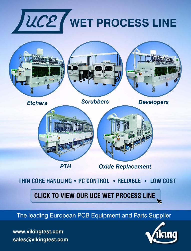
The leading European PCB Equipment and Parts Supplier
www.vikingtest.com
THIN CORE HANDLING • PC CONTROL • RELIABLE • LOW COST
CLICK TO VIEW OUR UCE WET PROCESS LINE
Etchers Scrubbers
PTH Oxide Replacement
Developers

18 PCB007 MAGAZINE I AUGUST 2019
their own facilities as well as the power and simplicity of these two standards.
IPC CFX and HERMESTo say the least, the buzz around these two
standards is palpable, and for six good reasons.
1. CFX Provides a Level Playing Field for Manufacturing CompaniesThis includes manufacturing companies of all sizes and in any location. Setting up IPC CFX in existing equipment can be accomplished in a matter of hours—not days—and the SDKs developed to make it easier are available free of charge.
2. Both Standards Provide a Simple Messaging Protocol for EquipmentThe messaging has been developed so that it can apply to new or legacy equipment. That means there’s no more need for custom pro-gramming for machine-to-machine messaging or middleware. Eliminating the need for mid-dleware reduces the eventual finger-pointing when adapters inevitably break.
3. The Standards Can Provide Significant Cost SavingsDeveloping a custom-built communications software, especially for multi-vendor equip-ment lines, can cost upwards of $30,000 and take up to a full business quarter to imple-ment. IPC CFX and HERMES are free to the industry, and companies have reported to IPC that they were able to implement CFX in less than one day.
4. The SDKs Serve as a Building Block for Enhanced Production TrackingIPC CFX and HERMES are written so that a company can easily and inexpensively add app-like functionalities for things such as ma-terials traceability or quality improvement.
5. CFX Is Flexible for Almost Any Piece of Equipment or Manufacturing Line One company loaded CFX into hand soldering tools, and IPC is receiving inquiries on how to implement CFX into non-electronics manufac-turing lines.
6. Instant Access to Real-time Data on Any Piece of Equipment WorldwideEMS sales representatives wanting to check availability of equipment for placing a new or-der or reporting a job status to OEM customers can view the activity of any piece of equip-ment in any facility, in any part of the world, in real time from their computer or handheld device.
This is just a sampling of the simplicity, val-ue, and power of IPC CFX and HERMES.
Collecting CFX RoadmapsHere’s what’s next for CFX. As interest in
IPC CFX grows, we regularly receive questions about timelines for implementation/CFX road-maps for equipment suppliers, software devel-opers, and EMS companies. To address this, IPC is collecting industry roadmaps for CFX implementation, and we plan to begin com-

AUGUST 2019 I PCB007 MAGAZINE 19
municating these to industry later this month.If you would like to provide your CFX road-
map, complete the roadmap form, and you should encourage your suppliers to do the same. Submit your completed roadmap form to Chris Jorgensen, IPC director of technology transfer, at [email protected].
Addressing Alternate Software Languages
IPC CFX was developed for .NET environ-ments, but as the first version of IPC-2591 was under development, the 2-17 Connected Fac-tory Exchange Initiative Subcommittee recog-nized the need to address software develop-ment kids (SDKs) for other languages in later versions. Groups are underway to develop SD-Ks for Linux, Python, Java, Node JS, and Lab-view. Once these SDKs are approved by the subcommittee, they will be available free of charge on the CFX GitHub website.
While the committee develops these new SDKs, they are seeking feedback from the in-dustry on the languages your organization and equipment support. Provide your feedback through this brief survey.
Version 1.1 Coming This YearTo meet the needs of industry, the 2-17 Sub-
committee has decided to put IPC-2591 on a twice-yearly revision schedule, and it has planned Version 1.1 for release by productron-ica in November. Version 1.1 will address new messages that the subcommittee was not able to include in the first version of the standard.
Version 1.1 will also address the alternate lan-guage SDKs and include any necessary modifi-cations to align with IPC-HERMES-9852.
How You Can Get InvolvedThere are ways you can begin aligning your
company with CFX and HERMES today:
1. Bring both standards in-house and ask your software support team to review them for implementation in your facility or with your equipment.2. OEMs and EMS companies should ask their suppliers for their CFX implementation roadmaps.3. Nominate one or more people from your organization to join the 2-17 Subcommittee, so you can comment on the draft IPC-2591 v 1.1 before we release it. Sign up and demonstrate your support for CFX here.4. Check out a live demonstration. IPC is planning CFX/9852 demonstrations at SMTAI in September, productronica in November, and IPC APEX EXPO 2020 in January. PCB007
Dr. John Mitchell is president and CEO of IPC—Association Connecting Electronics Industries. To read past columns or contact Mitchell, click here.

20 PCB007 MAGAZINE I AUGUST 2019
Feature Interview by Barry MattiesI-CONNECT007
Chemcut CEO and General Manager Rick Lies speaks about the growth he has seen in the marketplace over his 18 years in the in-dustry, and how Chemcut has been able to re-main competitive in the PCB and photochemi-cal milling spaces. Jerry Reitz, Chemcut’s HES manager, also addresses the current shift to-wards zero-discharge facilities.
Barry Matties: Can you start by telling us a little bit about Chemcut?
Rick Lies: Chemcut’s main market focus has been on making equipment for the wet pro-cessing industry that sprays chemicals, water, etc., across a moving conveyor populated with parts. We’ve been in business for over 60 years now. We started in the PCB and photochemi-cal milling industries, which involves the etch-
ing of different metals to make small or big parts of various sizes and dimensions out of a wide variety of metals. Over 60+ years, Chem-cut went from being a private company to be-ing acquired by Schering, then Atotech, and back to Chemcut as a private company in April 2002, so it has been 17 years. Now, we’re just an equipment manufacturer.
Matties: Is that an ESOP? Is Chemcut employ-ee-owned?
Lies: It’s not an ESOP, we are employee-owned; there are six of us now—we started with eight, but a few have retired and moved on. We bought it back from Atotech, so it went from Atotech back to Chemcut.
Matties: I remember all that transition.
Lies: And it has been going well. In the capi-tal equipment business, you always have your
Chemcut: Wet Processing Equipment for the Long Haul
Chemcut founder, the late Rufus Benton, in 1957.


22 PCB007 MAGAZINE I AUGUST 2019
ups and downs. We’ve lived through and survived those, and for the past three years, things have been go-ing well. We’ve entered in-to some new markets, but our traditional business in the PCB industry remains strong. Then, the photo-chemical milling industry picked up, and we’ve start-ed to get into semiconduc-tors and glass etching for flat-panel displays, etc.
Matties: How long have you been with Chemcut?
Lies: I’ve been with Chem-cut since I got hired at Atotech in July 2001, so since the inception of the new Chemcut.
Matties: And what did you do before Chemcut?
Lies: Before Chemcut, I worked 25+ years in a different industry, including at Avery Dennison, a worldwide leader in adhesive technology.
Matties: What is your background?
Lies: I have a degree in chemistry from the Uni-versity of Louisville.
Matties: So, you came into Atotech in chemis-try because that was a big play for them.
Lies: Yes. I worked with the chemistry and their equipment. They sold it as a package, and when the PCB market went over to Asia, they downsized the North American equip-ment.
Matties: Right. You entered at a time when the market was declining in North America.
Lies: Yes.
Matties: What were you thinking (laughs)?
Lies: Well, for me, it was all about location, loca-tion, location. We lived in State College, Pennsylva-nia, for close to 20 years—the longest my wife Maribel and I had ever lived in one place before; that was the first time I made a decision based on wanting to stay somewhere (laughs). It was time to settle down.
Matties: That’s great. It had to work because there were no options there (laughs). So, what was the challenge back then? At that time, Chemcut was six-years-old,
and by 2001, most of the industry was gone.
Lies: I think the challenge was to survive the first couple of years. Then, we wanted to keep our existing customers happy in PCB and pho-tochemical milling and let them know that we were still there because Atotech was mainly interested in selling their chemistry, and the Chemcut equipment brand needed to be high-lighted again as our main product line.
Matties: The brand got diluted.
Lies: Yes. When you look at Chemcut, the com-pany was primarily known for its subtractive processes. Atotech’s chemistry is more for ad-ditive type processes like plating. So, I like to say we divested ourselves of Atotech and had to get back out there with the Chemcut name in the subtractive area. That was good for us because we went from a large corporation to a small entity, and at the same time, there was the advent of websites.
Matties: High-speed internet came along right as that happened.
Lies: And that opened up the opportunity for Chemcut to market ourselves to the whole world. We didn’t need boots on the ground or
Rick Lies

AUGUST 2019 I PCB007 MAGAZINE 23
all of that printed material; we could get into Google searches. It was a different way to mar-ket your product, and it allowed us to market ourselves worldwide because our market is global.
Matties: I still see some of the original 547s out in the world.
Lies: Exactly. Chemcut equipment can last 10, 15, 20, and even up to 40 years. So, our equip-ment is still out there, chugging along. But that means your core customers—the equipment part of the business—change every year; you don’t get repeat business quickly. We’re start-ing to get repeat business for equipment we sold in 2003 and 2004 because, all of a sudden, that’s 15 years ago. Eventually, we need a new set of customers for our equipment side every year. Now, product support and service gener-ates a lot of repeat business. Over the past year, we probably have at least 500 customers world-wide that buy from us, anywhere from $10.50 for a part up to $1.5 million for a big line.
Matties: Hopefully, it weighs heavier on the high end (laughs).
Lies: Actually, the product support and service side of the business enables Chemcut to con-tinue to exist and service our broad customer base worldwide.
Matties: And it’s a lot less headache, too.
Lies: Exactly.
Matties: The market is still shifting, though. We’re seeing more and more thinking of additive and the smart factory mentality com-ing into play. How is that impacting your busi-ness?
Lies: What we have seen in the market is a shift to more roll-to-roll processes as well as a shift to more additive processes for larger vol-ume applications, which lend themselves to a smart factory mentality. At the same time, we have also seen a large demand for smaller
pieces of equipment for process development and smaller turns.
Matties: Right, and we’re at a flex show.
Lies: Which is why we are showcasing this reel-to-reel equipment. What you see behind us is actually an additive process, making a semiconductor smart label in the California ar-ea, and then there’s a plater that makes touch-screen products.
Matties: It’s a diverse line. What sort of team do you have for engineering?
Lies: We have both mechanical and electrical engineers. We’ve been able to beef that up mainly with strong Penn State University grad-uates from the area. A majority of equipment is PLC controlled, but we still have a good sec-tion of the market that want the tried and true relay logic.
Matties: What is it about Chemcut that people might not know that you want to share with them?
Lies: Our largest attribute is we make custom equipment to meet our customers’ specific needs. We also have a lab where you can come in if you have an idea or a concept, or you’ve done it in beakers or dip tanks, and want to develop a larger-scale manufacturing process for commercialization. We cannot manufac-ture millions and millions of pieces, but we do have a lab where you can come in, and we can show you how to do that. We work with a lot of companies, developing processes for them, and have had people come up to us already to-day and say, “We’re in R&D and have an idea. We need to do this.”
Our largest attribute is we make custom equipment to meet our
customers’ specific needs.

24 PCB007 MAGAZINE I AUGUST 2019
Matties: When you talk about the roll-to-roll pro-cess, how big is that? Is there a growing demand for that now?
Lies: More and more. We don’t make the roll-to-roll, but we work with people who do and integrate it into our equipment for their spe-cific manufacturing process.
Matties: The processing por-tion.
Lies: Right.
Matties: Are you seeing a higher demand for automation in North Amer-ica? I know we’re still talking low-volume, quick-turn, but it seems like there’s something there.
Lies: I don’t know if it’s really automation. It has been more about the data gathering to con-trol the processes, looking at it on a continu-ous basis, and making changes.
Matties: What about data gathering for legacy equipment? Is there a strategy to help custom-ers retrofit?
Lies: At times. Truthfully, not a whole lot, as it is an expensive retrofit after the fact. Chemcut is highly backward integrated. A lot of the parts that you see on a piece of Chemcut equipment are made at our company. When you need to re-place a part 30 years from now, we have our own molds that we make ourselves, and we’ve been able to supply parts that are over 50 years old.
Matties: We also talked a little bit about a boom in equipment sales earlier, and a lot of that was probably tied to the tax relief on the appreciation.
Lies: A portion of it is tied to tax relief, especial-ly for the people who haven’t re-tooled since
the early 2000s. So, there’s the portion of people who sat on their money, and now they’ve re-tooled, but a lot of our growth is in new mar-ket areas. Over the past two years, a good portion of our growth has been in North America. Part of it has been re-tooling, but we have also seen new technologies and customers becoming a large portion of our growth.
Matties: When people come back and buy new equip-ment now, what do they look for? Has their equip-ment worn out, or are they
looking for upgrading capabilities?
Lies: It’s a mixture. Some people don’t want to change what they already have, and we can provide them that, but then they might want better control of their conveyor system, which we now have at the lower speed end, especial-ly when it comes to reel-to-reel applications. Others might want better etching capability.
Matties: Along the way, it’s still pumps and nozzles. What about the green movement? We’re hearing a lot of zero-discharge conver-sations.
Lies: We’ve been involved with “zero-dis-charge” processes for our equipment for sev-eral years. How long have people doing zero discharge with our equipment, etc., Jerry?
Jerry Reitz: It has been nine or 10 years.
Lies: It’s not necessarily new technology; it’s out there, but it’s about how to integrate it into your particular process.
Matties: It’s about how you adopt it. What does it take for them to adopt it, and what’s the ad-vantage, other than not having to deal with the waste? Is there a financial gain as well?
Jerry Reitz

26 PCB007 MAGAZINE I AUGUST 2019
Reitz: There’s absolutely a financial gain. They’re not discharging their waste, so they’re not generating it, which is definitely a plus. It’s also easier for them to get permits to put in the equipment because local and state authorities like that movement, and some of our systems even recover the copper so that they can even get the copper back in full-sheet form.
Matties: When we visited GreenSource Fabri-cation in New Hampshire, Alex Stepinksi said he’s not buying any copper for his plating; everything he’s using is recycled. Why aren’t more companies doing that?
Reitz: That’s a good question. We try to push it with a lot of our customers, particularly those that are copper etching because it’s a very simple technology that’s available to them. However, I think it’s still something new to them.
Matties: Is it that they’re just unaware, or is it a complex system or a large investment? What are the obstacles?
Reitz: I think they just don’t understand how to effectively integrate these types of processes and understand the full benefit of integrating such technologies.
Matties: Maybe this is something we should start promoting.
Reitz: Absolutely.
Matties: It would make a big difference. Every-one is looking to lower cost, and this is a sure-fire way to do it. Otherwise, we just etch it off and recycle it.
Reitz: Right. You reduce waste, supplies, li-ability, and your operating costs all the way around.
Matties: It makes good sense. You’ve both been doing this for many years. If you were to give fabricators advice about your area, what would it be?
Reitz: Size your equipment so that it’s appro-priate for your operation. Don’t over-spec it or make it bigger than you need it to be. That’s what I find: a lot of customers who think they need a huge piece of equipment when, in real-ity, smaller equipment will do the same thing and offer a lot less operating cost and environ-mental impact, which results in an overall win for the entire project.
Matties: Do better planning up front.
Reitz: Yes, with utilities and everything. A lot of customers who call us still believe that you only need one machine; you get it, you plug it in, and you’re making circuit boards. However, they don’t understand all that goes along with it; it takes a lot of planning.
Matties: So, the best advice is if you’re getting ready to buy a piece of equipment, talk to you first not only about the equipment they want but also what they’re trying to achieve with the equipment because it’s easy to say, “I want this piece of equipment.” And it’s easy to sell it, but it’s better served if we all talk about it.
Reitz: Exactly.
Lies: And there’s another part to that, including the customer or the account, the equipment supplier, and the chemistry.
Matties: The chemistry supplier has to plug in-to this.
Reitz: Absolutely. It’s truly a team effort. You have to work with the chemical and equip-ment suppliers, facilities, and environmental people; it’s a group project. You can’t just buy a machine and plug it in; it’s a team effort.
Matties: That’s good advice. Thank you very much for your time.
Lies: Thank you very much.
Reitz: Thank you. PCB007

IPC Technology Solutions helps EMS providers and suppliers tackle increasingly complex operations and manufacturing challenges head-on with our five-prong approach:
Once an IPC Technology Solutions Expert uncovers the root cause of your issue and pinpoints the appropriate corrective action, they’ll deliver a confidential technical report with recommendations for process improvements. They’ll even educate your team on how to implement and sustain those improvements, and then follow up several months later to ensure our solutions are still working for you.
NO PROCESS CHALLENGE IS TOO BIG TO OVERCOME.
Enhance your operations. Solve supplier challenges. Improve your bottom line.
For more information, connect with the IPC Technology Solutions Experts at ipcvalidation.org/technology-solutions.
IPC TECHNOLOGY SOLUTIONS HAS YOUR BACK
FOLLOW UPEDUCATEPROBLEM-SOLVETROUBLESHOOTINVESTIGATE PROCESS

28 PCB007 MAGAZINE I AUGUST 2019
Feature Interview by Nolan JohnsonI-CONNECT007
Nolan Johnson chatted with George Milad, national accounts manager for technology at Uyemura about what is driving change in the wet process marketplace and how chemistries must fit into next-generation product design while also meeting new environmental re-quirements.
Nolan Johnson: George, regarding changes in wet processes, some market drivers are mov-ing, preserving margins, increasing yields, im-proving upon environmental concerns, and getting better capabilities and smaller features. From your perspective, where’s the market for wet processes going and what’s pushing it?
George Milad: Well, when you say wet process-es, you’re talking about chemical processes like board shop chemistries and where they’re headed. Mostly, there are developments in surface finishing and plating; those two areas are quite active. For example, the IPC Plating Committee also publishes specifications, and we are in the midst of revising the ENIG speci-fication.
Johnson: So, there’s the chemical process side as well as the equipment that is used. Is there more action in one of those two areas than the other, or are both of them in motion right now?
Milad: As far as the equipment, there are ten-dencies to automate. Water usage and environ-mental control in wet processing are also evolv-ing. Further, there are chemicals being used today that are not allowed on the REACH pro-gram environmentally. And there is an effort to minimize the use of these harmful chemicals, such as formaldehyde in electroless copper and cyanide in gold. There are new developments in surface finish to meet criteria, needs, and specific purposes, such as very fine-line work, as well as electroless copper plating via filling.
Johnson: In Richard DePoto’s interview with Pete Starkey from IPC APEX EXPO earlier this year, one of the points that stood out for me was his comment that Uyemura works to drop the chemistry right into existing lines. It seems that putting in a new chemistry/wet process line to hold a different line and set of chemi-
Putting Green Into a
Brownfield Facility
George Milad

Innovation + Precision + Reliability
ROLL-TO-ROLL PROCESSING• Processing for metals, thin foils, flexible glass and films
• Resist developing applications
• Cleaning applications
• Etching processes, including titanium and glass
• Aqueous based resist stripping
• Electroless plating processes
• Spray or immersion stations available for most applications

30 PCB007 MAGAZINE I AUGUST 2019
cals is a highly restrictive process for a lot of fabricators.
Milad: That is true. If I’m using chemistry from a certain supplier, and it’s not meeting my needs, and I want to change to a different sup-plier, it is very important that the supplier can fit their chemistry into my existing equipment and does not force me to buy new equipment. I think that’s what Richard was referring to.
Johnson: Pardon me for showing a lack of understanding of chemical engineering, but what goes into lining up the chemistries like that? For somebody who isn’t a chemistry ex-pert working with PCB fabrication, what is so different about the chemistries currently un-der development compared to what they used to be?
Milad: If you’re talking about under develop-ment, that is one thing. We were just talking about making the chemistry fit the existing equipment, but that’s a different issue after the development of chemical processes to meet new board designs. Designers are coming up with things that the present chemistries cannot meet, so they are moving forward with new chemistries to meet the designs. The new de-signs have much tighter lines and spaces and much smaller holes for next-generation, 5G-type products.
Johnson: How do you change the chemistry for that?
Milad: We have a substantial R&D team that is always looking forward to the next challenge, so they are very busy developing new prod-ucts. It’s not changing chemistries; instead, it’s a new set of products. Usually, they are de-signed to fit existing equipment. Sometimes, new equipment might be advantageous, but most of the time, they would develop products that fit the existing equipment.
For example, Uyemura is developing a gold bath that is cyanide-free, which is important; it’s not a requirement today, but it will be in the near future. We’re also developing chem-istries that are formaldehyde-free because it’s a hazardous chemical too. It is in use, and it’s not prohibited, but people are expecting that it will be and should be. There’s this direction based on meeting environmental needs, and then there is the development that is designed to meet more complex and sophisticated de-signs. We work on both ends to provide the chemistry for next-generation that will meet new environmental requirements.
Johnson: I know I’m talking in generalities here, but how long does it take to develop new chemistry like that?
Milad: The work in R&D is continuous. In gen-eral, Uyemura has about 60 people working in R&D, and they all have projects, looking forward, and are working to develop next-generation products. Sometimes, they devel-op them fast, but other times, it takes a while. It might work straight away when they try it, or they have to go back to the drawing board and redesign the product. It takes years to de-velop and test a product that is ready for the market.
The most important thing is that the market is constantly changing. This cycle is never go-ing to end. It’s not like all of a sudden, there will be no demands on the design and the en-vironment; the demands are going to continue indefinitely. Once I meet the design criteria of today with my chemical wet process, the next generation of design is going to come, and I’ll have to catch up with the designer and provide the chemistry they need. As soon as I’m there,
Designers are coming up with things that the present chemistries cannot meet,
so they are moving forward with new chemistries to
meet the designs.

AUGUST 2019 I PCB007 MAGAZINE 31
they’re on to the next design. It’s an endless cycle of product evolution and environmental restriction, which are both crucial. With wet process, R&D departments move a lot.
Johnson: Are the designers driving the market and what happens in chemistry development? Do you involve them?
Milad: Maybe the statement that the designers are driving everything is not totally accurate. It’s not the designer really, but the marketplace. The market says, “I need to go to 5G and make a more sophisticated prod-uct. I need it to be smaller, lighter, faster, and able to carry more memory.” That is market demand. Then, after the market demand, they go to the designer to design the product, and the designer is restricted by what is available to them. What’s available to them is what we (Uyemura) produce. We say, “We can give you these chemistries,” and so they work with that and respond, “I need more,” which forces us to consider new alternatives. Again, it’s a continuous cycle.
Johnson: I understand what you’re saying there, but I don’t think it’s an overstatement because the designers are the ones who have to take the conceptual market drivers and turn them into a real product. There is a point there where they are somewhat in charge. They’re the implementers. Do you involve the design-ers in your market research?
Milad: No, we don’t. We try to engage the OEMs themselves and understand what the needs are and what the next-generation prod-uct is going to look like, and then we acquaint them with our capabilities. We have a rela-tionship with the OEM, which is designed to keep the OEM abreast of our capabilities and keep us abreast of their future requirements. Of course, everything comes into play; they want a more sophisticated product, or they
want to meet the environmental constraints. They say, “This is the chemistry you’re using today. I would not be able to use that in a cou-ple of years from now. You need to develop a replacement for it.”
Johnson: As you’re talking to the OEMs, do you find that they’re more concerned about new capabilities and throughput?
Milad: Yes, they’re concerned about everything that comes into play, including capabilities, throughput, cost, etc. They’re trying to make
products, and they want to make sure that they’re affordable and available. And they do not like a good product that’s only made by one manufac-turer. They want to have choices and be able to source overseas if needed. They want to get compet-ing bids. So, if somebody
has the best process by itself, that doesn’t ex-cite an OEM; they want multiple suppliers. A single source doesn’t excite them at all, even if the product is the best thing after sliced bread.
Johnson: If they’re held captive to that and something goes terribly wrong, it’s a big prob-lem. That makes a lot of sense. How do you—as primarily a chemistry supplier—work to make sure that those processes are as repro-ducible across the globe at as many different facilities as possible?
Milad: It’s a challenge. Different parts of the world do things differently. Some shops that we refer to as “bucket shops” do work but they’re not high-quality or reproducible. Then, you have very sophisticated shops that do very high-quality work as well as small, remote, and big shops. There is a very wide variety of manufacturers, and we work with all of them. A big part of what we do is tech service. Our employees set up the shop and say, “Here is what you have to do.” But shops have differ-ent levels of engineering sophistication. Some

32 PCB007 MAGAZINE I AUGUST 2019
shops have very good engineering, while other shops have zero engineering and rely on the suppliers to give them all of the information.
Overall, wet processing development is being pushed by OEMs to meet sophisticated prod-uct requirements, which, at present, is where chemicals that are in use today are going to be phased out in a year or two. As a chemical supplier, we should be considering how we’ll do that. How are we going to eliminate these hazardous materials?
Johnson: While minimizing the amount of equipment that the fabricator has to purchase to move forward as much as possible.
Milad: Right. Sometimes, if you have a totally unique concept, you have different equipment; then, the customer knows up front that they will have to purchase new equipment if they are go-ing to use this process. But a lot of the processes that we develop are for customers who cannot afford to buy equipment all the time. They want the chemical process to fit into that existing fa-cility with their current equipment. We try to do that as much as possible.
Johnson: Is that common across the industry?
Milad: I think so. As a chemical supplier, we have competitors. But we collaborate when we’re try-ing to write a specification. After the specifica-tion is finalized, we compete against one an-other to try to sell our positive points, such as superior tech service or more robust chemistry.
Johnson: There has been a lot of work with Industry 4.0 at IPC, such as CFX and Hermes,
which were talked a lot about at IPC APEX EX-PO 2019 and since then. But it looks like most of the activity around CFX is on the assembly side.
Milad: I agree, but there is a lot of sophistica-tion also coming to manufacturing related to software and automated equipment; it doesn’t move as fast. There’s always room for that.
Johnson: One of the big burning issues, espe-cially in North America, is that most of the fab-ricators are nearing retirement age, and chang-ing market needs are going to cause them to need to change their processes, which may or may not need significant investment in new equipment. Many of them seem to be uninter-ested in making that investment.
Milad: It depends. If you know you’re going to make the investment and get a good return, you’ll make it. But a lot of people are just milk-ing what they have. I work with a board shop that has very poor equipment, and they strug-gle with it. They use old equipment to make products, and it’s tedious. They put a lot of demands on the suppliers, saying, “Make your chemistry work for my old equipment.” Last week, we were working with a board shop that acknowledged their equipment was not up to the task, but they wanted me to modify my wet process to accommodate that equipment. When that happens, sometimes, they’re suc-cessful in making products, but other times, they’re not.
You cannot have poor equipment and come to your supplier and say, “Make your chemis-try compensate for my inadequate equipment.” But we get that every now and then. Some board shops buy state-of-the-art equipment, have good engineering, and make very sophis-ticated products. Then, there are bucket shops making good money, but they work differently; they demand a lot from suppliers, like Uyemu-ra, because they’re trying to make a high-end product with sub-standard equipment.
Johnson: Thank you, George.
Milad: My pleasure. PCB007
As a chemical supplier, we have competitors. But we collaborate when we’re trying
to write a specification.


34 PCB007 MAGAZINE I AUGUST 2019
MilAero007 Highlightshigh-tech quantum device from the NUS Cen-tre for Quantum Technologies (CQT) is now orbiting in space together.
NASA Invests in 3D Printing for Aviation EAdditive manufacturing (AM), also known as 3D printing, is a promising new technology for all areas of aviation manufacturing. Additive manufacturing’s flexibility in design and cus-tomization, cost reduction, and speed in de-livering finished parts make it a perfect fit for creating parts used in aviation contexts.
‘Eyes’ for the Autopilot EAutomatic landings have long been standard procedure for commercial aircraft. While major airports have the infrastructure nec-essary to ensure the safe navigation of the aircraft, this is usually not the case at smaller airports.
Collins Aerospace’s David Adams Earns Dieter Bergman IPC Fellowship Award EIn recognition of his ongoing leadership in developing and promoting IPC standards on a global basis, IPC—Association Connect-ing Electronics Industries—bestowed a Dieter Bergman IPC Fellowship Award upon David Adams, Collins Aerospace, at the recent IPC SummerCom.
Aerospace Entrepreneur Burt Rutan to Keynote IPC APEX EXPO 2020 EIPC APEX EXPO 2020 will feature aerospace entrepreneur and Virgin Galactic spacecraft de-signer Burt Rutan. During the opening keynote on February 4, Rutan will present, “SpaceShi-pOne: A New Era in Commercial Space Travel and Inspiration for Innovation and the New Race for Space.”
NASA Seeks Input from U.S. Industry on Artemis Lander Development EIn a major step toward returning astronauts to the surface of the Moon under the Artemis lu-nar exploration program and preparing for fu-ture missions to Mars, NASA is seeking com-ments from American companies interested in providing an integrated human landing system to put the first woman and next man on the Moon by 2024.
Behind the Scenes of the Apollo Mission at MIT EFrom making the lunar landings possible to in-terpret the meaning of the moon rocks, the In-stitute was a vital part of history.
Math Invented for Moon Landing Helps Your Flight Arrive on Time EThey say the computers onboard the Apollo spacecraft were not even as powerful as your smartphone. So, how did they travel all that way, perform complex maneuvers in space, and return through Earth’s atmosphere at just the right angle to splashdown in the Pacific Ocean?
Lockheed Martin Wins $492M Contract for High-mobility Artillery Rocket System Launchers ELockheed Martin will produce High-Mobility Artillery Rocket System (HIMARS) launchers and associated hardware for the U.S. Army, U.S. Marine Corps, Romania, and Poland un-der a $492 million contract, marking Poland’s first acquisition of HIMARS launchers.
Of Art and Satellites EA quotation from The Golden Record 2.0—a play written for the NUS Arts Festival—and a


36 PCB007 MAGAZINE I AUGUST 2019
Feature Interview by Barry MattiesI-CONNECT007
I had the opportunity to sit with Mike Wood, technical director with Cerambus Asia Pacific, at the 2019 CPCA Show in China. Mike discusses the acid copper product from Cerambus Technology Inc. that doesn’t gen-erate sludge during the plating process and operates at higher production output by us-ing higher current density. This is important for the state of the vertical continuous plating (VCP) market in Asia, and trends he’s seeing in that space.
Barry Matties: You told me a little bit about your technology for the elimination of sludge in copper plating. Can you give us a quick overview?
Mike Wood: The Cerambus acid copper prod-uct has many advantages. One main advan-tage is that it does not generate sludge as you are plating production. Typically, in about two months, the bottom of the baskets build in sludge. Along with this, the distribution on the lower portion of the VCP hoist line drops and the bottom of the panels have a lower thick-
ness because the sludge is building and shield-ing the nuggets at the bottom of that anode basket.
So, our product essentially has no sludge. For one year, you could run your process and not have to empty or clean the baskets. Most people clean every three months, and they have to take a week out of production time to pull the nuggets all out. But they still have to do production, so during that downtime, the PC shop sends panels to an outside job shop. The downtime and cleaning are very expen-sive. It’s almost the same price as a full year of brightener when cleaning four times a year.
The second advantage is that without the sludge, you can have a better distribution, which also means higher plating amperage. This product will go above 30 amps per square decimeter (ASD) or 30 amps per square foot (ASF) current density and be very stable. I visited one customer, and in the past three months, the bath had no hand additions—only amp-hour replenishment at 38 ASF 24/7. To-day, with the high current density, new VCP machines in the market have increased the
The Advantages
of Non-sludge Acid Copper
ProductsMike Wood

‘Integrate’ QA solution by Gardien
Driving your profitability, maintaining your sustainable growth and enhancing yourbrand is all made possible with Gardien’s Integrate QA Solution
which comes with proper documentation and real-time tracking of the process.
Designed for and valued by PCB manufacturers worldwide, Gardien’s Integrate is an on-site, independent and unbiased validation of your board’s quality. Its focal points are your product
quality, e�ciency and transparency. All your PCB manufacturing QA needs, be it AOI, electrical testing, final inspection or a combination of these are fulfilled by Gardien experts located globally.
With solutions built around your unique requirements and a pricing structure that perfectly aligns with your business interests, your costs are more predictable and easier to budget.
Continuous Integration, Continuous Improvement
Find out more here:
www.gardien.com/why-integrate
30 YEARS OF PCBINDUSTRY EXPERIENCE
GLOBALLY LOCALDOCUMENTATION

38 PCB007 MAGAZINE I AUGUST 2019
eductor nozzles to a very high flow; it’s clos-er to two liters per minute per nozzle. At that high velocity, many of our competitors get thin at the knee. We don’t have that problem, so we can go to a very high current density from 34–38 ASF on these machines, increasing out-put by 20–30%.
Matties: So, you’re adding capacity.
Wood: Yes. Three VCP machines give the same output as four.
Matties: Obviously, this is a proprietary solu-tion. Why has it not been copied?
Wood: The technology is from the U.S., and we manufacture the concentrate there—and in a facility in Asia—so the key ingredients are manufactured and controlled by us. For five years, others in the industry have tried to copy it but have not been successful.
Matties: It sounds like the ROI is straightaway?
Wood: Absolutely. John Nash, my boss [and Ce-rambus president], has said to many custom-ers, “Don’t pay us for the brightener. Give us all of the savings that you receive from a lower operating cost.” No purchasing agent has tak-en him up on it yet, but that speaks volumes.
Matties: I also understand that Cerambus con-tinues to expand.
Wood: Yes, we’re expanding into other markets. We’re doing a lot of work in Thailand, and we’re expanding into Southern Asia with the rest of the PC shops. We’re also expanding into the more rural areas of China and business is going very well. We have a very good market share, and we’re doing a lot with these advantages.
Matties: I would think your market share is in-creasing pretty quickly.
Wood: It is. We have a very high growth be-cause of those advantages, and people are buy-ing more VCPs.
Matties: When I spoke with John [Nash], he mentioned a new technical center. Can you talk about that?
Wood: Of course, we have our Dongguan fa-cility that is a manufacturing and technology center, and we are planning to move from the San Jose area to the Las Vegas area with R&D and manufacturing.
Matties: How do you see the market right now?
Wood: Most people are going into the VCPs for consistency, and the end customer wants it. So, since our product works best with VCP, we see a little softening. But our sales continue to grow, and I see some more demand when I visit Thailand; there’s a lot more demand there for buyers that want to have a fallback if any-thing happens regarding the trade war.
Matties: That seems to be a frequent topic of conversation in China. When you look at the Chinese market, how many years have you been here?
Wood: Cerambus has been here for many years, over 15. But over time, people haven’t realized the advantages, and purchasing staff inside China are now understanding what the operating cost is compared to the price. So, instead of what the price per liter is if they analyze the full cost, that’s when we expand our business.
Matties: The level of sophistication in Chinese manufacturing has increased as well.
Wood: Yes, we’ve witnessed that. One of the things that I’ve noticed for some of the auto-motive is they now use conformal microvias on the outside of the board. We had one customer who was running at 8 ASF with a competitor in VCP, and now they’re running a through-hole and that microvia 6x5 deep at 27 ASF. So, our chemistry has some big advantages.
Matties: What advice would you give to a fab-ricator in China?

AUGUST 2019 I PCB007 MAGAZINE 39
Wood: Right now, you have a lot of inter-nal growth. I just heard that retail in Chi-na was at a 14-year low, so that may have an impact. There may be a slowdown that will consolidate the market. At this point, if I were a PCB company, I would continue what I was doing and look for cost efficiency and final yield. Often, the chemistry cost is nothing compared to the final yield; if you can improve 0.5%, then all of your savings would be there.
Matties: Those are all bottom-line dollars.
Wood: Absolutely.
Matties: Is there anything we have not discussed that you would like to share with the industry?
Wood: I believe the one thing that people are doing to lower their cost is to buy a piece of automated equipment—VCP sys-tems. The advantage of VCP is if one an-ode is bad, you have another 99 of them, so you lose less than 1% of your thick-ness distribution on one side—one out of 100. But if you have a hoist and that an-ode is sitting in the middle of your panel, you can plate low thickness and create scrap. Right now, everybody is moving toward VCP because they want a high output with low coefficient of variation (COV). To pay for it, they want the high-est plating amperage and plating speed, so the key area is efficiency. We can save money on metal consumption over many months and no anode sludge. I also see automation utilizing robots for loading and unloading of panels, and the equip-ment suppliers are doing a good job of taking advantage of improvements in de-sign.
Matties: Well, we certainly appreciate your time today. Thank you.
Wood: Okay. Thank you. PCB007
Mobile Performance Report Shows
Incredible Speeds on 5G Compared to LTE
South Korean operator LG U+ held an edge over the com-petition in Seoul by delivering the fastest 5G speeds and lowest latency among all networks while also providing out-standing 5G data reliability, according to the first in a series of 5G First Look Reports by RootMetrics—the standard for mobile performance benchmarking by IHS Markit. The report discusses 5G performance by South Korean operators KT, LG U+, and SK Telecom, offering insights into the world of 5G and how 5G networks perform from the consumer’s perspective.
Key takeaways from the report include:• Each operator’s median download speeds on 5G were much faster than those on non-5G mode or LTE• All three operators were on 5G during at least 42.2% of RootMetrics download tests• KT and LG U+ led the way with latency with both operators’ 5G median download latency twice as fast as that recorded in non-5G mode• Operator highlights: All networks show dramatic speed improvements on 5G
LG U+ had a 5G median download speed of 426.4 Mbps that would take only 12s to download a 600MB TV show. Although KT delivered the slowest 5G median download speed across all networks at 163 Mbps, it would still only take about 30s to download a TV show at this speed. Meanwhile, SK Telecom delivered a 5G median download speed of 286.9 Mbps.
(Source: IHS Markit)
40 PCB007 MAGAZINE I AUGUST 2019
High-density interconnect (HDI) demands that vias that do not contain component leads be plugged with either a polymeric paste or electroplated copper. In this column, the tech-nology drivers for via filling/plugging in the context of HDI are presented.
Performance-driven electronic systems con-tinue to challenge companies in seeking a more innovative semiconductor package methodol-ogy. The key market driver for semiconductor package technology is to provide greater func-tionality and improved performance without increasing package size. As semiconductor die elements shrink in size, companies are seek-ing to further increase package density and en-hance functional performance. This, in turn, drives designers to expand the current role of the interposer to interconnect both heteroge-neous logic functions and homogeneous mem-ory within a single package outline.
The package interposer is the key enabler; this is especially true as glass-reinforced, ep-oxy-based materials, and high-density copper
interconnect capability will continue to carry a primary role for array configured packag-ing. From a PCB fabrication standpoint, engi-neers must adopt the manufacturing processes to include via fill and via plugging technolo-gy. I will dive into details of these processes over the next few editions of “Trouble in Your Tank.” However, this particular column will fo-cus on the need for via filling and some of the methods used to carry out the process.
Why Fill Vias?Microvias, buried vias, and plated through-
holes are filled with conductive or non-con-ductive materials for a number of reasons:
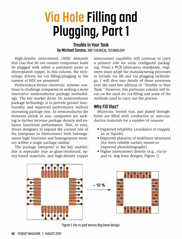
• Improved reliability (avoidance of trapped air or liquids)• Improved planarity of multilayer structures (for more reliable surface mount or improved photolithography)• Higher interconnect density (e.g., via-in- pad vs. dog bone designs, Figure 1)
Via Hole Filling and Plugging, Part 1
Trouble in Your Tankby Michael Carano, RBP CHEMICAL TECHNOLOGY
Figure 1: Via-in-pad versus dog bone design.

burkleamerica.com
Contact:Kurt Palmer714-379-5090

• Better thermal management• Density, density, density• Increased I/O number for packaging
applications• Minimized signal delays and to avoid
defects associated with electromigration• Enables stacked microvia structures
(often seen in smartphones’ boardtechnology, Figure 2)
Via-in-pad reduces the footprint as well as increases the density. This design concept places the via directly below the component contacts and reduces the footprint when com-pared to fan-out. When via-in-pad is used in a design, there will be the call-out for via filling or plugging process (more on the process op-tions for via filling in a future column). Filling the via that is in the pad will improve the bond strength of the component when mounted over the filled via (Figure 2).
The concern with the issue shown in Figure 2 is that air inclusions during the lamination process may reduce long-term reliability. An additional concern with air inclusions is that, in effect, air is an insulator. Thus, air reduces both electrical and thermal conductance. While it is acceptable to endure very small voids in the via simply due to processing and material
properties, it is desirable to minimize air voids through material property selection, via plug-ging techniques, and equipment designs [1].
In the next few columns, I will present over-views of the different via fill technologies avail-able. Meanwhile, one must first understand the definitions used for via fill and/or via plug-ging. While this distinction may seem trivial, it must nonetheless be clearly communicated between the board supplier and end user (as agreed between user and supplier, or AABUS).
Figure 3 shows a schematic of an HDI struc-ture containing through-holes, blind and buried vias, and microvias. Via hole filling is used for
Figure 2: Component mounted on unfilled vias (note the air pockets).
Figure 3: HDI structure. (Source: Happy Holden)
42 PCB007 MAGAZINE I AUGUST 2019

AUGUST 2019 I PCB007 MAGAZINE 43
the non-planar filling of plated through-holes. Via hole plugging is synonymous with the pla-narization of blind and buried vias as well as through-holes. Via hole plugging is applicable to HDI and microvia designs. Brushing (or pla-narization) is required to remove the excess ma-terial and create the flat surface. This technique is described in previously published papers [1 &
2]. And there are some applications where the vias will be filled by a copper electroplating pro-cess commonly known as superfilling.
Superfilling or bottom-up filling of vias re-quires specialized plating processes, process controls, and plating cell set-up. This will also be the subject of a future column.
For the circuit board designer, the goal is to construct an architecture with flexible designs to ensure higher I/O densities as well as lower costs and greater performance. As Figure 3 de-picts, there are four common via architectures for HDI:
1. Drill sequential lamination2. Staggered sequential microvia build-up3. Co-laminated any layer via stack microvia build-up4. Stacked sequential microvia build-up
Yield issues are more difficult to pin down because they depend on a number of vari-ables and are largely statistically driven (i.e., the greater the occurrence of a certain con-figuration will influence yields). Regardless, the four types of structures are used in HDI fabrication based on design constraints and routing density. PCB007
References1. K. Andra, “Hole Plugging Technology for Multilayers
and HDI Packages,” EPC PCB Convention, 1999. 2. S. Kramer and M. Suppa, “Via Hole Filling and Plug-
ging: Trends, Possibilities, and Limitations for Convention-al and SBU-type Fillers,” IPC Printed Circuit Expo 2001.
Michael Carano is VP of technology and business development for RBP Chemical Technology. To read past columns or contact Carano, click here.
New Filter Enhances Robot Vision on 6D
Pose EstimationA recent study
was conducted by researchers at the University of Illinois at Urbana-Cham-paign, NVIDIA, the University of Wash-ington, and Stan-ford University on 6D object pose esti-mation to develop a filter to give robots greater spatial per-ception so that they can manipulate objects and navi-gate through space more accurately.
While 3D pose provides location information on X, Y, and Z axes, 6D pose gives a much more complete picture. “Much like describing an airplane in flight, the robot also needs to know the three dimensions of the object’s orientation—its yaw, pitch, and roll,” said Xinke Deng, a doctoral student studying with Timo-thy Bretl, an associate professor in the Department of Aerospace Engineering at the U of I.
Deng explained that the work was done to improve computer vision. He and his colleagues developed a filter to help robots analyze spatial data. The filter looks at each particle, or piece of image information collected by cameras aimed at an object, to help re-duce judgment errors.
The study uses 6D object pose tracking in the Rao-Blackwellized particle filtering framework where the 3D rotation and the 3D translation of an object are separated. This allows the researchers’ approach, called PoseRBPF, to efficiently estimate the 3D trans-lation of an object along with the full distribution over the 3D rotation. As a result, PoseRBPF can track ob-jects with arbitrary symmetries while still maintaining adequate posterior distributions.
(Source: University of Illinois)

44 PCB007 MAGAZINE I AUGUST 2019
Article by Peter Moleux with contributions from Happy Holden
The first step in any pollution prevention
strategy is to minimize chemical wastes and their rinse waters. There are five general cat-egories of common techniques for pollution prevention in a PCB fabrication facility:
1. New processes to replace sources of pollution2. Extend the bath’s life3. Rinse water reduction4. Dragout reduction5. Ventilation reduction
While this list is not all-inclusive, it provides an overview of the types of technologies used around the world that are important to consid-er. In this article, we will examine rinse water reduction.
Rinse Water ReductionMost of the waste generated in the manufac-
turing of PCBs is from cleaning, plating, strip-ping, and etching. This section describes some
of the techniques available for reducing the volume of rinse water used.
While we stress the need to reduce individu-al rinse water flow rates when a conventional wastewater precipitation system is anticipated, there may be at least one possible exception. If in excess of 95% of all chemicals are recov-ered, the chemicals do not enter the rinse wa-ter collection system, and a central membrane filtration or deionization system is used to pro-duce a zero-effluent system; then, the need to reduce rinse water flow is reduced. However, one must also consider the capital and operat-ing costs for the central system.
One author wrote the following concerning rinse flow rates in the case of a zero-effluent system [1].
“It should also be noted that in a well-engi-neered zero liquid discharge environment, wa-ter conservation is unnecessary. Instead, the focus is total dissolved solids (TDS) budgeting throughout the plant, along with an analysis of specific critical contaminants. Water supply is only limited by the size of the pumps. For instance, to maximize absorption in the fume


46 PCB007 MAGAZINE I AUGUST 2019
scrubber, 10 gallons/minute of DI water can be fed continuously into and out of the scrubber system reservoir… With a closed-loop system, there is no sacrificing of rinse quality to save water. Lift stations integrated with conductiv-ity sensors can automatically identify an out-of-control waste stream as it happens, allowing for quick corrections by maintenance. Also, fresh rinse-water conductivity is always DI quality.”
Particulate Filtration on Deburr and Panel-scrubbing Operations
Deburrers are used to remove stubs of cop-per formed after the drilling of holes in double-sided and multilayer panels before they enter the copper deposition process. Scrubbers are used to remove oxides from printed circuit laminates, clean the surface prior to a surface coating to provide better adhesion and remove residuals after etching or stripping. In deburr-ing and board scrubbing, particulate materi-als are added to the water and are removed by various methods based on size and the weight of the copper particle such that the wash wa-ter becomes suitable for up to 100% recycling. The types of filtration available for this opera-tion are cloth, sand, centrifugation, and gravity settling with filtration.
Etcher and Conveyorized Equipment Design Modifications
Etching machines can be the single largest source of copper waste in the discharge from a PCB facility. The amount of copper discharged, and the rinse flow rate from that machine, is a function of the machine design.
An older etching machine will contain a single-stage etchant replenishing module po-sitioned between the etching chamber and its continuously flowing single or multiple stage water rinse chamber. Fresh etchant is fed to the replenishing module to wash the panels, and that etchant (now containing copper washed from the freshly etched panels) then flows (in a direction opposite to the direction of the pan-el movement) into the etching chamber. The continuous water rinse can contain from 100 to 500 milligrams per liter (mg/l or ppm) of
copper, depending on the configuration of the rinse module. Companies that use this type of equipment, with a single-station rinse module, normally have floor space restrictions in their production area. The etcher design affects the rate of etchant solution dragout as does the vol-ume of panels being processed and the quality of the etchant solution control.
By way of comparison, adding a second stage replenisher station will reduce the range of copper dragout in the following rinse from 50 mg/l to 300 mg/l. We have observed more than one etching machine–using a four-stage replenisher module and a combination of wa-ter recirculating with a single-stage rinse mod-ule–produce a rinse effluent containing from less than 1.0 mg/l up to 2.0 mg/l of copper. That is the option that we recommend to cli-ents when etchant recycle, and copper recov-ery are not practical or economical.
Use of recirculating rinse modules will de-crease the required flow rate of rinse water (by about 50%) without requiring significantly more floor space, compared to single-station spray rinse chambers (without recirculating rinses). In this application, fresh water is used for the final top and bottom nozzles in a rinse module. This water is collected in a sump lo-cated below the rinsing compartment. A pump recirculates this water through the first set of top and bottom nozzles (instead of using fresh water). As more fresh water enters the sump, the excess water overflows through a pipe fit-ting to drain. While recirculation modules are available for purchase, they can also be cus-tom-built by each PCB factory.
If a PCB factory must evaluate the purchase of a new etching machine, we recommend that a photoelectric cell be included on the load module to sense when panels are being pro-cessed. This can be used to activate and deac-tivate the rinses on that machine. Water used for rinsing will begin to flow only when a pan-el enters a rinse chamber, and a timer will de-termine (based on the speed of the conveyor belt carrying the panels) when the last panel will exit that rinse chamber.
The rinse water inlet connection to any rinse chamber should be fitted with a flow restrictor
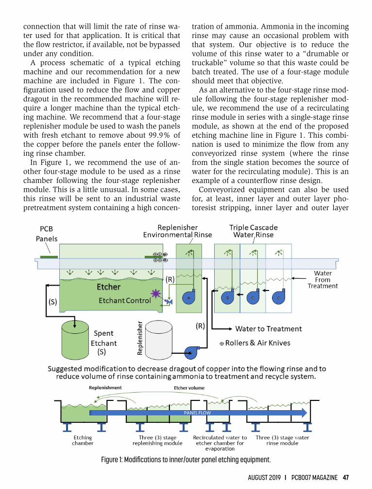
AUGUST 2019 I PCB007 MAGAZINE 47
connection that will limit the rate of rinse wa-ter used for that application. It is critical that the flow restrictor, if available, not be bypassed under any condition.
A process schematic of a typical etching machine and our recommendation for a new machine are included in Figure 1. The con-figuration used to reduce the flow and copper dragout in the recommended machine will re-quire a longer machine than the typical etch-ing machine. We recommend that a four-stage replenisher module be used to wash the panels with fresh etchant to remove about 99.9% of the copper before the panels enter the follow-ing rinse chamber.
In Figure 1, we recommend the use of an-other four-stage module to be used as a rinse chamber following the four-stage replenisher module. This is a little unusual. In some cases, this rinse will be sent to an industrial waste pretreatment system containing a high concen-
tration of ammonia. Ammonia in the incoming rinse may cause an occasional problem with that system. Our objective is to reduce the volume of this rinse water to a “drumable or truckable” volume so that this waste could be batch treated. The use of a four-stage module should meet that objective.
As an alternative to the four-stage rinse mod-ule following the four-stage replenisher mod-ule, we recommend the use of a recirculating rinse module in series with a single-stage rinse module, as shown at the end of the proposed etching machine line in Figure 1. This combi-nation is used to minimize the flow from any conveyorized rinse system (where the rinse from the single station becomes the source of water for the recirculating module). This is an example of a counterflow rinse design.
Conveyorized equipment can also be used for, at least, inner layer and outer layer pho-toresist stripping, inner layer and outer layer
Figure 1: Modifications to inner/outer panel etching equipment.

48 PCB007 MAGAZINE I AUGUST 2019
photoresist developing, deburring, and panel scrubbing. Similar techniques to reduce water flow can be applied to these operations.
Both the volume of wastewater and its cop-per content may be minimized by selecting a properly designed new or modifying existing conveyorized machine. The numerous options presented in this section must be evaluated on a case-by-case (and site-by-site) basis. Please be aware that some of our recommendations for waste minimization require additional floor space in the production area, that may not be currently available.
Before a final decision is made to purchase or to modify a machine, it is advisable for each PCB factory to weigh the alternative equipment and operating costs. However, if the available production floor space is already stretched too thin, this comparison and its effort may be a waste of time.
Use of recirculating rinse modules in the etcher and other conveyorized equipment will decrease the required flow rate of rinse water for that process step by about 50% without requiring significantly more floor space, com-pared to single-station spray rinse chambers (without recirculating rinses). In this applica-tion, fresh water is used for the final top and bottom nozzles in a rinse module. This water is collected in a sump located below the rinsing compartment. A pump recirculates this water through the first set of top and bottom nozzles (instead of using fresh water). As more fresh water enters the sump, the excess water over-flows through a pipe fitting to drain (Figure 1).
Conveyorized equipment can also be used for, at least, inner layer and outer layer photo-resist stripping and inner layer and outer layer photoresist developing, deburring, and panel scrubbing. Similar techniques to reduce water flow can be applied to these operations.
Immersion-type Counterflow RinsesCounterflow rinsing, employing several sin-
gle-stage rinse tanks in series, is one of the most powerful waste reduction and water manage-ment techniques for inner layer processing and in the electroless copper process. These opera-tions use a cage-type carrier that holds many inner layer panels in a side by side configura-tion for processing. Immersion rinsing of pan-els is also required following the cleaner bath in the pattern plating operation and in other operations.
While multiple tanks can be connected in series, we prefer using one properly designed counterflow rinse tank to minimize floor space requirements. However, this opportunity to reduce the rinse flow rate does require more floor space than a single-station rinse tank.
In counter-current rinsing, after exiting the process bath, the boards move through several rinse contact stages, while water flows from stage to stage in the opposite direction. Over time, the first rinse reaches a steady-state con-centration of process dragout contaminants that is lower than the process solution. The second rinse (away from the process bath) stabilizes at even a lower concentration. This enables less water to be used to produce the same cleanliness compared to a single-station rinse tank. The higher the number of rinse sta-tions connected in series, the lower the rinse rate needed for adequate removal of the pro-cess solution from the panel.
A multistage counterflow rinse system al-lows greater contact time between the panels and the rinse water, greater diffusion of the process chemicals into the rinse water, and more rinse water to encounter each panel. The disadvantage of multistage rinsing is that more steps are required as well as additional equip-ment and workspace. Generally speaking, it is impractical to use more than a four-stage rinse
Before a final decision is made to purchase or to modify a machine, it is advisable for each PCB factory to weigh the alternative equipment
and operating costs.


50 PCB007 MAGAZINE I AUGUST 2019
tank. Conventionally, a two-stage rinse which has been properly designed should be suffi-cient to minimize flow. Typically, a two-station counterflow rinse requires 2–3 U. S. gallons per minute (gpm) of rinse water compared to 5–10 gpm for a well-used single-station rinse. A three-station rinse requires only 1–3 gpm. A four-station rinse may be used when a rinse must be collected and batch treated in a small volume. For initial planning purposes, a dilu-tion ratio of 1,000 to 1.0 is used to determine proper rinsing.
Every rinse tank water inlet pipeline should contain a flexible orifice-type flow restric-tor limiting the flow rate of water while the rinse tank is in use. For constantly used rins-es, continuous low flow is desirable (for ex-ample, where selective ion exchange systems will be used to remove copper). Under other conditions, water use should be intermittent. For these applications, a solenoid valve, timer, and activation system (a tank- or wall-mount-ed push button or a foot peddle, which is less desirable) should be provided.
Turn off the rinse water when the rinse is not required. This can be accomplished on convey-orized equipment by installing photoelectric cells and/or timers on the immersion rinses to activate and deactivate the water inlet lines only when required. Just being able to activate a rinse and deactivate a rinse when the ma-chine is activated is not enough.
Alternating Side Spray Rinses Side pulsating spray rinses for the acid cop-
per and etch resist plating lines are an alter-native to flood rinsing to conserve water. We recommend evaluating the use of single-stage pulsating spray rinses in place of immersion rinses in acid copper plating lines. The reduc-tion in water consumption using a pulsating spray rinse is about 85–90% of that consumed using an immersion-type rinse.
In practice, the fan-type water spray pattern would first be applied to one side of the panel, and then the source of water would alternate to spray the other side of the panel. This will require two (normally closed) solenoid valves for each rinse station where the spray system
is used. The system would be activated by a wall- or tank-mounted push button. When the spray rinse is activated, its instantaneous flow rate may be as high as 95 lpm (25 gpm). How-ever, the rinse would only be activated when a panel requires rinsing, and the panel is located within a specific rinse tank. For example, as-suming a one-minute immersion time for each load of (or “work rack” carrying) panels and 30 loads during a 40-hour week, the weekly average rinse flow rate could be as low as 1.1 lpm (0.31 gpm) compared to 18.9 lpm (5 gpm). That is a reduction of 94% for just that flow rate.
Another advantage of spray rinsing is that it will eliminate the need to dump the entire contents of an immersion-type rinse tank, for cleaning purposes, on a periodic basis.
Flexible Orifice-type Flow Restrictor Fittings (If Available)
The use of flexible orifice-type flow restric-tors with timers may be more efficient than conductivity controllers for immersion-type rinse tanks. We recommend the use of a flex-ible orifice-type flow restrictor located on the water inlet to every immersion-type rinse tank. We are not in favor of using conductiv-ity sensors unless they can be calibrated at least once per week. Conductivity controllers are useful when one desires to reduce water consumption.
One reason to use a conductivity controller is when one must collect and then batch treat a rinse if that rinse cannot effectively be treat-ed in the continuous wastewater treatment system. The purpose of an efficient conductiv-ity controller is to reduce the volume of waste, the floor space required, and the cost required to treat a specific waste.
With conductivity sensors, the rate of rinse water flow into a rinse tank is a function of the water inlet pipe size (diameter) and the water pressure in the pipeline. The larger the pipe and the higher the pressure, the higher the rinse water flow rate. A conductivity control-ler is used to open or close a valve based on measuring the cleanliness of the water in the rinse tank (assuming the conductivity probe is
AUGUST 2019 I PCB007 MAGAZINE 51
located properly). Solenoid valves are electri-cally actuated valves that are commonly used with conductivity controllers. A solenoid valve is either fully open or fully closed; its purpose is not to control the rate of water flow.
Flow restrictors, if available, are ordered based on the desired flow rate (we recommend a 2–3-gpm flow restrictor for a two-stage coun-terflow rinse tank) and the pipe size. If a mini-mum water pressure exists in the water inlet line (about 20 psi is considered minimum), the water flow into a rinse tank should not vary although the water pressure will most likely vary. Flow restrictors are not adjustable after they are installed. By providing pipe union fit-tings for both up and down of the flow restric-tors, adjustments can be made. Flow restric-tors with flexible diaphragms are rated for a specific flow rate in a specific pipe size. Typi-cally, a 2–3-gpm flow restrictor is recommend-ed for a two-stage counterflow rinse tank. If a minimum water pressure exists in the water inlet line (about 20 lbs/in2 is considered mini-mum), the water flow into a rinse tank should not vary, although the water pressure will most likely vary. Flow restrictors are not ad-justable after they are installed. By providing pipe union fittings both up and downstream from the flow restrictor fitting, the flow rate can be changed if necessary.
We recommend installing a flexible orifice-type flow restrictor or an automated control system to maintain and monitor the inlet water flow rate to every rinse tank. Existing conduc-tivity sensors, if any, should be removed, unless they can be calibrated at least once per week. When rinse recycling or recovery equipment is to be specified, a designer must be aware of the maximum flow rate. The installation of a flow restrictor provides that assurance (if all rinse water passes through that restrictor).
Reuse of Rinse Water in the Electroless Copper Process
Chemical suppliers occasionally recommend the reuse of rinse water within an electroless copper line. This may require the use of pumps to transfer water from one rinse tank to an-other. As one alternative to reduce the volume
of waste, we recommend that at least one of the possibilities noted in Figure 1 be tested at each facility in the short term to determine the effect. This opportunity should be discussed with the technical representatives of the chem-istry supplier for that process line before the final decision is made to implement this task. The critical element is not to recycle rinse wa-ter upstream around the catalyst. It would be useful to have a detailed chemical analysis of the rinse water before having discussions with your chemical supplier.
Dragout Reduction by Using a Deionized Water Mist Spray as the Panels Are Withdrawn From a Heated Bath
This should be evaluated for, at least, the brown oxide bath and the etchback bath. Installing specially designed rollers and air knives to reduce the dragout from panels being etched and following the dragout still rinse station should be considered. Some plat-ing rack designs allow the panels to be tilted to one side and the panel mounted at an an-gle (relative to the horizontal) to allow better solution drainage off the panel. This will de-crease the dragout.
Eliminate the Need to Strip Racks on the Acid Copper and Tin-lead Line
By using plastic-coated racks, only the tips and contactors (that electrically and physically connect and support the panel to the carrying rack), having exposed conductive metal, must be stripped. We recommend evaluating the use of racks with disposable contactors. That would eliminate the need to strip the racks and could eliminate the use of nitric acid. These types of racks are commercially available and should be addressed in the short term.
Increase the Amount of Agitation in the Immersion Rinse Tanks
Agitation between the panels and the rinse water can be performed either by moving the panels in water or by creating turbulence in the rinse water. Since most PCB factories operate hand rack lines, operators could easily move workpieces manually by moving the rack.
52 PCB007 MAGAZINE I AUGUST 2019
However, the effectiveness of this depends on the cooperation of the operator.
Agitating the rinse tank by using oil-free low-pressure air (from a blower, not an air compressor) is the most efficient method for creating effective turbulence during rins-ing operations. This type of agitation can be performed by pumping filtered air into the bottom of a rinse tank through a pipe dis-tributor (air sparger). Air volumes typically recommended are 3–4 cubic foot per minute per square foot of rinse tank surface area. The delivered pressure should be about 1 psi for every 21 inches of liquid depth. Not ev-ery rinse tank should be agitated. There may be selected rinses that will produce excessive foam when agitated. Care should be used be-fore agitating rinse tanks.
Dragout ReductionBath dragout reduction can reduce recovery
equipment and operating costs. Withdraw the panels slowly to allow ample drainage. The faster an item is removed from a process bath, the thicker the liquid film is on the panel, and the greater the dragout volume will be. The removal of racks containing panels is opera-tor-dependent (unless automated hoists are used); therefore, the amount of dragout from each bath will be operator-dependent. The time allowed for drainage can be inadequate if the operator is rushed to remove the rack from the process bath and place it in the rinse tank. However, the installation of a rail above the process tank and the requirement that the operator place all racks on the rail for at least 10 seconds will reduce the dragout.
However, there are a few operations where concern about oxidization of the panel will not allow this method to be used to reduce the dra-gout.
Etcher DesignIn the last section, we described the prop-
er design for an etcher. In that case, a four-stage replenisher module reduced the dragout of etchant contaminated with copper more ef-ficiently than a two-stage replenisher module. However, the four-stage (or even a three-stage) replenisher module requires more floor space than a two- or a single-stage module. If etchant recycling is contemplated, the etcher itself may be redesigned (eliminating the need for a re-plenisher module).
Increasing Dwell TimeHolding the panels over the process bath re-
duces the dragout. One can accomplish this ei-ther by slowly withdrawing the panels from a process bath or by installing a rigid supporting device to hang the rack with the panel over the process tank, for a period, before proceeding to the rinse tank.
Use of Automated Control and Wet Processing Systems
Computerized process control systems can be used for panel handling and process bath monitoring to prevent unexpected decomposi-tion of a process bath, controlled rinse flow, and uniform panel withdrawal from each pro-cess bath. Since these systems require a sig-nificant capital expense for initial installation, only large PCB companies will incorporate this alternative into their manufacturing process.
Drip PansA drip pan (also called a drain board) is
one of the simplest methods for dragout re-covery. The drip pan will capture drips of pro-cess solution from racks and panels as these are transferred between tanks. Drip pans not only save chemicals and reduce rinse water re-quirements, but they also improve housekeep-ing by keeping the floor dry. We also stress the need for double containment of all plumbing
Not every rinse tank should be agitated. There may be selected rinses that will produce excessive foam
when agitated.

Your Passport to Global PCB Sourcing
REDMOND, WASHINGTON • TUCSON, ARIZONA • GLOBAL PARTNERSHIPS
AS-9100D(888)847-7686
PROTOTRON.COM
We are pleased to announce that with the same fine service, quality, delivery and attention to detail that our customers have grown to rely upon, we are now adding a complete global solution to meet all of your needs, both today and in the future.
FLEX & RIGID-FLEX
HDI / MICROVIA
COMPETITIVE VOLUME PRICING
PRE-QUALIFIED OFFSHORE PARTNERS
QUICK-TURN PROTOTYPES
COMPLEX MULTILAYER
MIL-SPEC PRODUCTION
SPECIALTY MATERIALS
Our Solutions: • • • •
• • • •

54 PCB007 MAGAZINE I AUGUST 2019
to prevent leaks of corrosive chemicals onto the floor. Spillage from a process tank, pipe, chemical mixing area or etcher must be antici-pated and methods provided to contain, col-lect, analyze, and process the liquids.
AutomationComputerized process control systems can
be used for panel handling and process bath monitoring to prevent unexpected decomposi-tion of a process bath, controlled rinse flow, and uniform panel withdrawal from each pro-cess bath. Since these systems require a sig-nificant capital expense for initial installation, typically, only large PCB companies will find this to be a cost-effective alternative.
DI and Soft Water for RinsingNatural contaminants found in water used
for production purposes can contribute to the volume of waste produced. Silicates are a known contaminant in PCB chemistries. When using pretreated rinse water, the water require-ments for each rinse are reduced.
Printed Circuits Handbook: Sixth Edition [2]
states that many water supplies contain high levels of dissolved ionic minerals and possible colloidal materials that cause rejects in board production. Some of these impurities are cal-cium, silica, magnesium, iron, and chloride. Typical problems caused by these impurities are copper oxidation, residues in the plated through-holes (PTH), copper-to-copper peel-ing, staining, roughness, and ionic contami-nation. Equipment problems due to these im-purities include, but are not limited to, water line and water spray nozzle clogging, corro-sion, and other mechanical breakdowns. Pro-cess baths should be made using deionized water.
The presence of organics in water can ad-versely affect etching and another bath perfor-mance. Very good water may contain no more than 2.0 ppm of total organic carbon. The best plating practices suggest using good water quality for critical rinsing operations and high yields. While what is considered good water quality is not precisely defined, here are com-monly used criteria:
• Total dissolved solids (TDS) 4–10 mg/l (or ppm)• Conductivity 8–30 microsiemens/cm• Carbonate hardness 3–15 ppm• Chloride 2.0 ppm• Turbidity 1.0 NTU
Somewhat lower quality is acceptable for less critical applications (deburring) while some other operations (for example, the developer rinse) require better water, such as water con-taining only 0.5–5 ppm of TDS (0.1–1 MEG). However, this depends on several factors.
One article [3] explained, “Aqueous dry film resists are susceptible to over development. If left too long in the developer, the exposed re-sist will be chemically attacked and will par-tially disintegrate…A short residence time in the development chamber helps minimize re-sist swelling.”
Additional swelling that may cause adhesion failure must be avoided in the rinsing cham-ber. Distilled or deionized water used in the first developer rinse may rapidly penetrate the resist due to osmotic pressure. This may dilute the higher ionic strength developer solution trapped in the resist. To avoid this, the first rinse should have, according to this article [3], a relatively high ionic concentration by adding salts.
Water hardness in the first rinse of 140–350 mg/L of CaCO3 is adequate for most work. If the rinse does not have sufficient hardness, use an acidic second rinse.
Another article [4] claimed that sufficient hardness must be available in the water used for the developer working solution makeup and the developer rinse for some resists. In those cases, magnesium sulfate has been add-ed to the water when sidewall definition and resist toughness needs improvement. Other critical rinses are:
• The accelerator• The catalyst• The last rinse on the electroless copper line• Before and following nickel• The gold and palladium electroless/electroplating
baths

AUGUST 2019 I PCB007 MAGAZINE 55
The methods used to achieve these charac-teristics of water are beyond the scope of this series. Most resin and equipment suppliers rec-ommend (or require) the use of softened water for this final (and sometimes every) washing stage. The requirement for soft water implies that the incoming unused process water must be processed to remove the hardness (calcium and magnesium ions) before it can be used for the final rinse in an exchange column. PCB007
References1. A. Stepinski, “21st Century PCB Fab Factory Design,
Which Eliminates Regional Cost Advantages,” IPC APEX EXPO Proceedings, 2017.
2. C.F. Coombs Jr., Printed Circuits Handbook: Sixth Edi-tion, McGraw-Hill, 2008.
3. K.H. Dietz, “Probing the Limits of Dry-Film Resist,”Printed Circuit Fabrication, Vol. 16, No. 6, June 1993, p. 24.
4. K.H. Dietz, “Fine-Line Imaging: Trends in Exposure and Development Technology,” Printed Circuit Fabrication, Vol. 18, No. 10, October 1995, p. 32.
Pete Moleux is a chemical, environmental, health, and safety engineering advisor who has served industrial clients and law and expert witness search firms since 1988.
Happy Holden has worked in printed circuit technology since 1970 with Hewlett-Packard, NanYa/Westwood, Merix, Foxconn and Gentex. He is currently a contributing technical
editor with I-Connect007. To read past columns or to contact Holden, click here.
“The innovation lies in the advanced materials devel-opment using molecular beam epitaxy (MBE) to ‘grow’ the compound semiconductor crystal in an atom-by-atom re-gime. This particular material is rather complex and chal-lenging to synthesize as it combines four different atoms requiring a new MBE methodology,” said Professor Huf-faker. “The Sêr Cymru MBE facility, partly funded by HE-FCW, is designed specifically to realize an entire family of challenging materials targeting future sensing solutions.”
Dr. Shiyu Xie, Sêr Cymru Cofund Fellow, said, “The re-sults we are reporting are significant as they operate in a very low-signal environment, at room temperature, and very importantly, are compatible with the current InP op-toelectronic platform used by most commercial communi-cation vendors.
The APDs have a wide range of applications. In LIDAR, or 3D laser mapping, they are used to produce high-resolution maps with applications in geomorphology, seismology, and in the control and navigation of some autonomous cars.
The findings can change the global field of research in APDs. The material developed can be a direct substi-tute in the current existing APDs, yielding a higher data transmission rate or enabling a much longer transmis-sion distance.
(Source: Cardiff University)
Cardiff University researchers have developed a com-pound semiconductor (CS) technology that can drive fu-ture high-speed data communications. A team from the Institute for Compound Semiconductors (ICS) worked with collaborators to innovate an ultrafast and highly sensitive avalanche photodiode (APD) that creates less electronic noise than its silicon rivals.
A paper outlining the breakthrough in creating extreme-ly low excess noise and high sensitivity APDs is published in Nature Photonics.
Cardiff researchers led by Sêr Cymru Professor Diana Huffaker, scientific director of ICS and Sêr Cymru Chair in Advanced Engineering and Materials, partnered with the University of Sheffield and the California NanoSystems Institute, University of California, Los Angeles (UCLA), to develop the technology.
Cardiff Delivers Compound Semiconductor Breakthrough
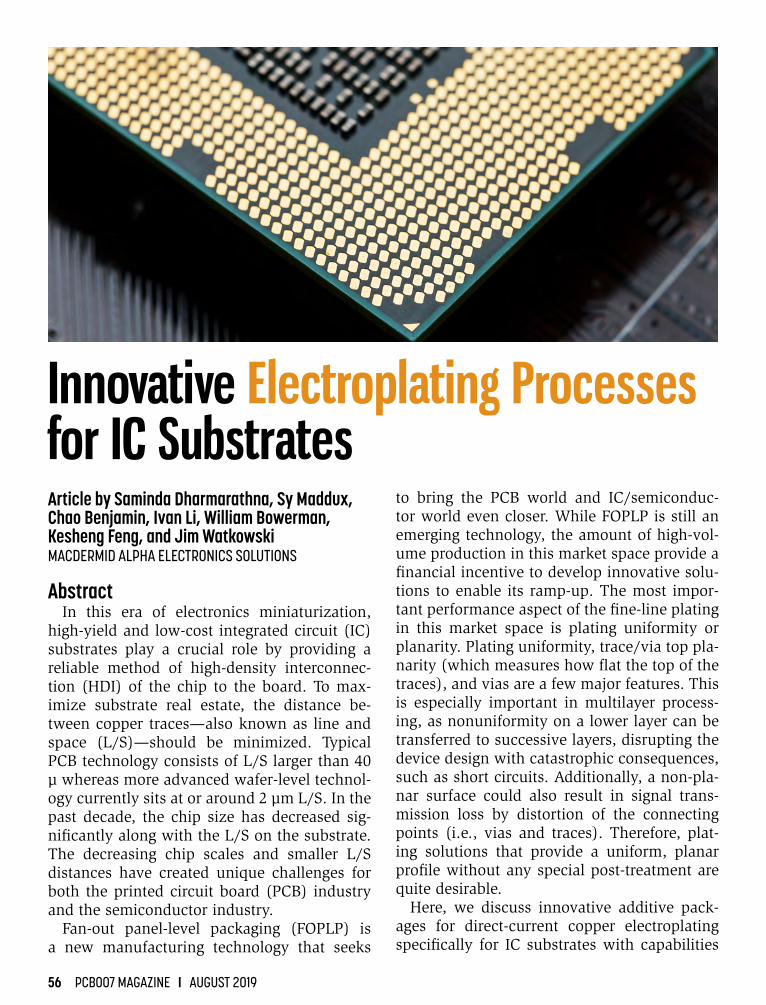
56 PCB007 MAGAZINE I AUGUST 2019
Article by Saminda Dharmarathna, Sy Maddux, Chao Benjamin, Ivan Li, William Bowerman, Kesheng Feng, and Jim WatkowskiMACDERMID ALPHA ELECTRONICS SOLUTIONS
AbstractIn this era of electronics miniaturization,
high-yield and low-cost integrated circuit (IC) substrates play a crucial role by providing a reliable method of high-density interconnec-tion (HDI) of the chip to the board. To max-imize substrate real estate, the distance be-tween copper traces—also known as line and space (L/S)—should be minimized. Typical PCB technology consists of L/S larger than 40 µ whereas more advanced wafer-level technol-ogy currently sits at or around 2 µm L/S. In the past decade, the chip size has decreased sig-nificantly along with the L/S on the substrate. The decreasing chip scales and smaller L/S distances have created unique challenges for both the printed circuit board (PCB) industry and the semiconductor industry.
Fan-out panel-level packaging (FOPLP) is a new manufacturing technology that seeks
to bring the PCB world and IC/semiconduc-tor world even closer. While FOPLP is still an emerging technology, the amount of high-vol-ume production in this market space provide a financial incentive to develop innovative solu-tions to enable its ramp-up. The most impor-tant performance aspect of the fine-line plating in this market space is plating uniformity or planarity. Plating uniformity, trace/via top pla-narity (which measures how flat the top of the traces), and vias are a few major features. This is especially important in multilayer process-ing, as nonuniformity on a lower layer can be transferred to successive layers, disrupting the device design with catastrophic consequences, such as short circuits. Additionally, a non-pla-nar surface could also result in signal trans-mission loss by distortion of the connecting points (i.e., vias and traces). Therefore, plat-ing solutions that provide a uniform, planar profile without any special post-treatment are quite desirable.
Here, we discuss innovative additive pack-ages for direct-current copper electroplating specifically for IC substrates with capabilities
Innovative Electroplating Processes for IC Substrates


58 PCB007 MAGAZINE I AUGUST 2019
such as embedded trench fill and simultaneous through-hole plating and via filling with an en-hanced pattern plate. These new solutions not only offer better trace profile, but they also de-liver via fill and through-hole plating. We also describe two electrolytic copper plating pro-cesses, the selection of which could be based on the via size and the dimple requirements of the application. Process I offers great via fill for deeper vias up to 80–120 µm diameter and 50–100 µm deep (Figure 1). Process II is more suitable for shallow smaller vias 50–75 µm di-ameter and 30–50 µm deep.
In this article, we show that these two pro-cesses provide excellent surface uniformity and trace profile (Figure 2) while also provid-ing via filling and through-hole plating capa-bilities when controlled within given param-eters. Process optimization and thermal and physical characterization of the metallization are also presented.
IntroductionThe IC substrate is the high-
est level of miniaturization in PCB technology, providing the connection between the IC chip and the PCB. These connections are created through a network of electrically conductive copper traces and through-holes. The density of the traces is a crucial factor in terms of miniaturiza-tion, speed, and portability of consumer electronics. Trace den-sity has grown immensely over the past few decades to meet today’s printed circuit designs, which include thin core material, fine-line widths, and smaller di-ameter through-holes and blind vias. The development of fan-out
panel-level packaging (FOPLP) has been a top-ic among the microelectronics community for some time.
The main driving forces to push this new technology are cost and productivity. Tradi-tional fan-out wafer-level packaging (FOWLP) uses a 300-mm wafer as the production vehi-cle because larger wafers are difficult to ob-tain. Therefore, the FOWLP has a limitation on the basic unit of process, thereby increas-ing the processing steps, manpower, and cost while also having a low yield. The advantage of using a PCB-like substrate is that manufac-turers have more design flexibility and surface area compared to the wafer. As an example, a 610 x 457 mm panel has almost four times the surface area of a 300-mm wafer [1]. Therefore, processing a panel this size drastically reduc-es cost, time, and processing steps. This is a huge advantage for the high-volume produc-tion market.
Figure 1: Capability of the processes for simultaneous via fill and through-hole plating with enhanced pattern plating.
Figure 2: Embedded trench fill performance of the formulation, showing uniform height between pads and lines.

AUGUST 2019 I PCB007 MAGAZINE 59
However, applying FOPLP technology to substrate scale poses challenges that require more research and development. These chal-lenges are the resolution and warpage issues of FOPLP technology. If successfully implement-ed, this new technology will reshape consumer electronics resulting in higher production, low-er cost, thinner package sizes, and faster and lighter consumer electronics [2].
Acid Copper Via FillElectrodeposition is one of the crucial steps
in developing a circuit board, as this is where the network for routing electrical current is plated onto the PCB board as traces, vias, and through-holes. Copper is the conductive metal of choice due to several advantages, such as its cost and relatively high electrical conductivity. Therefore, usage of copper as an electroplat-ing metal has grown immensely over the last few decades as having the methods of plating it. Advanced, proprietary board designs re-quire cutting-edge plating tools and innovative solutions. As a result, within the last few de-cades, impingement plating tools have become a widespread tool among the plating industry.
Copper via filling baths typically have high concentrations of copper (up to 200–250 g/L copper sulfate) and lower concentrations of acid (approximately 50 g/L sulfuric acid) to promote rapid filling. Organic additives are used to control the plating rate and obtain ac-ceptable physical properties. These additives must be designed carefully to tailor the cus-tomer needs, such as the size of the vias filling requirements, yield, surface copper thickness, copper distribution tolerance throughout the panel, and the shape of the via after plating. Typical plating formulations will contain car-riers, brighteners, and levelers. In theory, it is possible to fill vias with only a two-component system that includes a carrier and brightener. However, there are practical issues with two-component systems, such as large dimple size, conformal fill, and difficulty analyzing for pro-cess control.
Both carriers and levelers act as suppressors but can be classified in different ways. Type I suppressors like carriers can be deactivated by
the brightener whereas Type II suppressors like levelers do not undergo deactivation. Carriers are typically high molecular weight polyoxyal-kyl compounds [3]. Usually, they are adsorbed on the surface of the cathode and form a thin layer by interacting with chloride ions. Hence, the carrier reduces the plating rate by increas-ing the effective thickness of the diffusion lay-er [4]. Consequently, the energy level over the cathode surface topography is being equalized (the same number of electrons become avail-able locally for plating at all cathode surface spots) so that the resultant deposit becomes more uniform and evenly distributed.
On the other hand, brighteners increase the plating rate by reducing suppression. They are typically small molecular weight sulfur-con-taining compounds, also called grain refiners. Levelers typically consist of nitrogen-bearing linear/branched polymers and heterocyclic or non-heterocyclic aromatic compounds that are typically quaternary in structure (central positively charged atom along with four sub-stituents). These compounds will adsorb se-lectively on high current density sites, such as edges and corners and local protrusions, and prevent copper over plating in high cur-rent density areas [5].
Test MethodTests were completed in an 8-liter plating
cell and 200-liter pilot tanks. Insoluble anodes were used for higher applicable current densi-ties, easy maintenance, and a uniform copper surface distribution. Each bath was made up,
These compounds will adsorb selectively on high current
density sites, such as edges and corners and local protrusions,
and prevent copper over plating in high current density areas.

60 PCB007 MAGAZINE I AUGUST 2019
dummy plated for 1 Ah/L, analyzed, adjust-ed to correct additive levels, and then the test panel was plated. Each test panel went through a pre-clean cycle of one-minute acid cleaner, one-minute rinse, and one-minute 10% sulfu-ric acid before the plating.
Conditions and Bath ComponentsTable 1 shows the operational conditions
and optimum additive levels for the two for-mulations. Typically, via fill baths have high copper and low acid to achieve the desired bottom-up fill.
Via Fill MechanismThe growth rate of copper inside the via
and on the surface of the panel is controlled by the additives. Figure 3 shows a schematic representation of via copper growth. The dif-ferent role played by each additive is shown. Even though the adsorption is exaggerated and shown as highly localized, both selec-tive and non-selective adsorption occur dur-ing plating. Additive compositions must be
controlled in the set range shown in Table 1 to achieve the desired “bottom-up filling.” Common analytical tools used in the indus-try such as cyclic voltammetry striping (CVS) analysis and hull cell plating may be utilized for this.
In Figure 3, the suppressor is shown in green, the leveler in red, and the brightener in yellow. Wetter molecules are mainly adsorbed on the surface suppressing the plating there, while the leveler adsorbs selectively on to the negatively charged areas, due to the positively charged quaternized N group. This prevents over plating at the edges and avoids prema-ture closure of the via, which could result in voiding in its center. The brightener, being a small, sulfur-containing molecule, diffuses faster into the via and accelerates the plating. As the geometry of the via changes continu-ously during the plating process, the bright-ener becomes concentrated inside the via causing rapid plating in the via. This is called the curvature enhanced accelerator coverage (CEAC) mechanism [6].
Table 1: Bath components and plating conditions.
Figure 3: Schematic representation of CEAC mechanism (suppressor is shown in green, leveler in red, and brightener in yellow).

www.entelechyglobal.com
We deliver the highest quality PCB CAM and MechanicalCAD engineering services to customers around the world.
.
Having trouble keeping up with front-end demand?We have people for that.
• Increased on-demand capacity• Improved automation• Faster turn-around times• Reduce costs• Improved quality• Ability to build redundancy in critical areas
Here are six ways that outsourcing CAM and related front-end work can help manufacturers not only stay in business but also help them thrive:
Find out how we can help you >

62 PCB007 MAGAZINE I AUGUST 2019
Finally, when the copper plating inside the via approaches coplanarity with the surface, the plating rates inside of the via and on the surface become equal, and the bottom-up fill-ing stops. However, depending on how strong the additive adsorbs and desorbs, the bright-ener may not diffuse as expected, and the high concentration of the brightener will keep ac-celerating the plating, resulting in over-plate referred to as a “momentum pump.”
Fine-line Profile MeasurementFigure 4 shows the calculation of the profile
% and the R-value. The profile % is defined as the ratio between the height difference of the lowest and highest points and expressed as a percentage, while the R-value is the
height difference between the pad area and fine lines. Minimum values for both numbers are desirable.
Process I is designed to fill vias with flat tops and to plate fine lines with better trace profile %; therefore, the plating conditions are opti-mized as shown in Table 1. To achieve desired via fill capability, higher CuSO4 concentration (200 g/L) was used in combination with low sulfuric acid (50 g/L).
Typical performance of Process I is shown in Figure 5 in which vias 60 x 35 µm in size were filled while the total surface Cu thickness was 15 µm. Due to the ability of Process I to fill the vias with minimal dimple, no additional planarizing steps are necessary. Profile % was generally in the range of 10–15%; however,
there were a few instances where it was observed be-tween 15–20%. Plated Cu thickness for the lines was 15–16 µm. The R-value was between 1–2. Pad shape was closer to square and had a flat top while lines showed a slight dome.
Further evaluation of the via filling capability of the formulation was done using vias of different sizes. Four different via sizes were test-ed: 90 x 25 µm, 80 x 35 µm, 90 x 60 µm, and 100 x 80
Figure 5: Typical plating performance of Process I.
Figure 4: Profile % and R-value calculation.

AUGUST 2019 I PCB007 MAGAZINE 63
µm. Results are shown in Figure 6. As shown, no dimple was observed up to 90 x 60 µm via filling. However, larger vias—such as 100 x 80 µm—had a 4 µm dimple.
Bath Life StudyAfter the initial performance evaluation, a
bath was aged up to 150 Ah/L. The volume of the bath was 8 L. The plating cycle for each plating was 15 ASF for 45 minutes, and addi-tive concentration was the same as tabulated in Table 1.
During the aging, a test panel was plated at every 50 Ah/L, cross-sectioned, and evaluated under the microscope. The test board consist-
ed of 60 x 35 µm vias and with various L/S for fine lines. Plating cycle was adjusted to ob-tain around 15 µm on the surface. Throughout the aging process, the lines showed Profile % in the range of 10–15% and occasionally 15–20% consistent with the initial performance tests. R-value was between 1–2 with flat pad plating.
Through-hole fill capability was tested using board thicknesses of 40 and 60 µm. Hole di-ameters were 40 and 50 µm, respectively, for the two boards. Results are shown in Figure 7. Plating cycle was 1.24 ASD for 60 minutes. As shown in Figure 7, the X-hole filling was excel-lent with Process I.
Figure 6: Filling capability of different size vias 90 x 25, 80 x 35, 90 x 60, and 100 x 80 µm, respectively.
Table 2: Bath aging test results profile % for 18/25, L/S, and R-value up to 150 Ah/L.

64 PCB007 MAGAZINE I AUGUST 2019
Tensile Strength and ElongationTwo of the most important physical prop-
erties to PCB manufacturing are the tensile strength and % elongation of the plated cop-per conductors because these properties are in-dicative of the ability for the copper metal to withstand the thermal stresses incurred during assembly and end-use. The physical properties are a result of the combined influence of the additives, suppressor, grain refin-er, and leveler. These properties also depend on the plating rate or current density, temperature at which the plating is done, and the crystal morphology. For instance, densely packed equiaxial depos-its will have better physical prop-erties than a columnar deposit.
Physical properties were mea-sured according to the IPC TM-650, 2.4.18.1 test method. Sample strips were extracted and baked in an oven at 125°C for four to six
hours. An industry mechanical test instrument was used to test the strips. The measurements from this instrument were used to calculate tensile strength and elongation %. Figure 8 shows the results at two different bath ages: a fresh bath and a bath aged around 100 Ah/L. According to the results, the properties did not change much with the bath age and passed the IPC Class III requirements.
Figure 7: X-hole filling capability of Process I.
Figure 8: Physical properties, tensile strength, and elongation of Process I fresh and aged baths.


66 PCB007 MAGAZINE I AUGUST 2019
Internal StressUnder the influence of additives, the plat-
ed metal deposit will have some residual in-ternal stress. Many factors—such as tempera-ture, thickness, additives, and annealing—will affect stress. Stress could be either tensile or compressive. In both cases, high stress is det-rimental to the PCB board, causing distortion in the final board called warping. We used an internal stress analyzer to measure the stress of the deposit as plated and after annealing.
To measure the stress, first, a test strip was immersed in a cleaner solution at 45°C for up to 30 seconds and rinsed with water. Then, the strip was dried completely and weighed. Next, the strip was plated at the desired current den-sity for the desired time to achieve the neces-sary Cu thickness. Finally, the strip was rinsed with water and dried very carefully with low-pressure air. Then the strip was mounted on the measuring stand (deposit stress analyzer). The value for U was measured and recorded as the sum of the total number of measure-ment increments on both sides of the zero on the measuring stand. The plated test strip was weighed, and the final weight was recorded. After the deposit thickness is known and the number of increments spread between the test strip leg tips has been determined, the deposit stress can be calculated using the equation S = UKM ÷ 3T where S = pounds per square inch, U = measured number of increments spread, T = deposit thickness in inches, K is the strip calibration constant, and M equals the modu-lus of elasticity of the deposit divided by the modulus of elasticity of the substrate material.
After the initial measurement was done, the strips were annealed at 130°C for one hour. Figure 9 summarizes the internal stress data for Process I with fresh and aged baths with both plated and annealed strips. Low internal stress under 1000 psi was observed for both plated and annealed conditions, and this did not change significantly as the bath ages.
Deposit Grain StructureThe grain structure of the deposit was stud-
ied using focused ion beam (FIB) microscopy techniques. Plated copper samples from fresh
and aged bath were evaluated. Figure 10 shows the grain structure of the deposit. In the fig-ures, the top portion of the fine grain struc-ture is the plated copper from Process I and the bottom portion with larger grains are from the internal stress test strip substrate. Both images are at 5000x magnification. According to the data, the grain structure remained unchanged even after aging the bath.
Embedded Trench Plating FormulationProcess II is tailored towards embedded
trench plating applications with higher acid (200 g/L) than CuSO4 (100 g/L) in contrast to Process I, which promotes the via fill. Results are summarized in Figure 11. However, we tested Process II and its via fill capability by changing the VMS by increasing CuSO4 to 250 g/L. According to Figure 11, an average dimple around 3–4 µm was seen in vias of 60 x 35 µm size with surface Cu of 10–15 µm. However, Process II showed excellent embedded trench plate capability with high coplanarity with the
Figure 9: Internal stress of the copper deposit plated using Process I, both as plated and annealed data for fresh and aged baths.
Figure 10: Grain structure with bath age, (a) fresh bath, (b) 100 Ah/L.

AUGUST 2019 I PCB007 MAGAZINE 67
R-value of only 0.37 in the given example. The tops of the trenches were square-shaped.
Process II was optimized to obtain square-shaped trenches. Inorganic components, Cu-SO4, acid, and chloride were optimized, as
summarized in Figure 12. Lower CuSO4 and high acid gave a better trench shape than the high CuSO4 and low acid.
Further, the physical properties of Process II were measured, specifically tensile strength
Figure 11: Via fill and trace plate capability of Process II.
Figure 12: Trace plate with varying VMS for Process II.

68 PCB007 MAGAZINE I AUGUST 2019
and elongation for the fresh and aged bath. As shown in Figure 13, the tensile strength and elongation % for Process II passes the IPC Class III requirements of tensile strength great-er than 36,000 psi and elongation greater than 18%.
ConclusionsTwo innovative processes for acid copper
metallization in IC substrates were presented. The objective was to achieve planar via fill and flat profiles for fine-line applications and for higher uniformity of embedded trench designs between the pad height and fine-line height. The formulations reported here showed excel-lent via fill capability and fine-line profile %. Excellent uniformity between the pad and fine-line areas was obtained. The deposits produced by these formulations were shown to have low internal stress, both plated and annealed. The
physical property of tensile strength and elon-gation produced by these deposits was stable as the bath aged and passed IPC Class III. A com-bined summary of these is shown in Table 3. All of the additive components utilized in these processes can be analyzed with common ana-lytical tools used in the industry. PCB007
References1. T. Braun, K.-F. Becker, S. Voges, J. Bauer, R. Kahle,
V. Bader, T. Thomas, R. Aschenbrenner, and K.-D. Lang, “24”×18” Fan-Out Panel-Level Packaging,” IEEE/ECTC Pro-ceedings, 2014, pp. 940–946.
2. T. Braun, K.-F. Becker, M. Wöhrmann, M. Töpper, L. Böttcher, R. Aschenbrenner, and K.-D. Lang, “Trends in Fan-Out Wafer and Panel-Level Packaging,” International Conference on Electronics Packaging (ICEP), Yamagata, 2017, pp. 325–327.
3. P. Broekman, A. Fluegel, C. Emnet, M. Arnold, C. Roeger-Goepfert, A. Wagner, N.T.M. Hai, and D. Mayer, “Classification of Suppressor Additives Based on Syner-gistic and Antagonistic Ensemble Effects,” Electrochimi-ca Acta, Volume 56, Issue 13, May 1, 2011, pp. 4,724–4,734.
4. K.B. Herbert, S. Adhikari, and J.E. Houser, “Chemical Mechanism of Suppression of Copper Electrodeposition by Poly (Ethylene Glycol),” Journal of the Electrochemical Society, 152 (5), C324–C329, 2005.
5. S. Dharmarathna, I. Li, M. Sy, E. Zeng, B. Wei, W. Bow-erman, and K. Feng, “High-Throw DC Acid Copper Formu-lation for Vertical Continuous Electroplating Processes,” IPC APEX EXPO 2017, February 14 –16, 2017.
Figure 13: Physical properties, tensile strength, and elongation of Process II fresh and aged baths.
Table 3: Comparison of the tensile strength and elonga-tion % of the via filling focused Process I and the embed-ded trench focused Process II, fresh vs. aged 50 Ah/L.

AUGUST 2019 I PCB007 MAGAZINE 69
This paper was first presented at the IPC APEX EXPO 2019 Technical Conference and published in the 2019 Techni-cal Conference Proceedings.
Ivan Li is no longer with the company.
Jim Watkowski is VP of innovation circuitry solutions at MacDermid Alpha Electronics Solutions, Waterbury, Connecticut, USA.
Maddux Sy is applications manager at the MacDermid Alpha Circuitry Solutions Global Development Application Center in Taiwan.
Benjamin Chao is business manager at the MacDermid Alpha Circuitry Solutions Global Development Application Center in Taiwan.
6. Y. Zhang, G. Ding, P. Cheng, and H. Wang, “Numeri-cal Simulation and Experimental Verification of Additive Distribution in Through-Silicon Via During Copper Filling Process,” Journal of The Electrochemical Society, 162 (1), D62–D67, 2015.
Saminda Dharmarathna is principal R&D chemist at MacDermid Alpha Electronics Solutions, Waterbury, Connecticut, USA.
William Bowerman is director of primary metallization at MacDermid Alpha Electronics Solutions, Waterbury, Connecticut, USA.
Kesheng Feng is research director, metallization, at MacDermid Alpha Electronics Solutions, Waterbury, Connecticut, USA.
To test the system, they used a microscope to moni-tor fluorescently labeled microparticles in liquid as they flowed through the microchannel. When acetylcholine was applied, the muscle contracted. The resulting force was transduced to a bar that was pushed down to close
the valve, which successfully stopped the flow of liquid. When the acetylcholine was washed away, the muscle relaxed, the valve re-opened, and the fluid flowed again.
“Now that we have shown that on-chip muscle-driven valves are possible, we can work on improve-ments that will make it practical,” says first author Yo Tanaka from RIKEN BDR. “One option is to use cultured muscle cells. This might enable mass-production, better control, and flexibility in terms of shape.”
(Source: RIKEN)
A team of researchers from the RIKEN Center for Bio-systems Dynamics Research (BDR) and Tokyo Denki Uni-versity has been developing a bio-MEMS (microelectro-mechanical systems with living material) that is driven by real muscle, which could be useful in surgical implants. Building on their on-chip micro-pump design, the new study is the proof-of-concept for an on-chip muscle-driven valve.
The team initially determined that a small 1x3 cm sheet of earth-worm muscle could produce an average contractile force of about 1.5 mN over a two-minute period when stimulated by a very small amount of acetylcholine. Using this data, they build a microfluid channel and valve on a 2x2 cm microchip that could be controlled by the contraction/relaxation of earthworm muscle.
Cyborg-like Microchip Valve Driven by Earthworm Muscle

70 PCB007 MAGAZINE I AUGUST 2019
Semiconductor Industry Capex Forecast to Slump in 2019 and 2020 EIn its upcoming mid-year update to The Mc-Clean Report 2019, IC Insights reports that the semiconductor industry capex is forecast to slump in 2019 and 2020. Over the past 34 years, there have been six periods when semicon-ductor industry capital spending declined by double-digits rates for one or two years (1985–1986, 1992, 1997–1998, 2001–2002, 2008–2009, and 2012–2013).
5G Smartphones Shipment to Reach 1.9 Billion, Overtaking 4G in 2023 ECanalys expects 5G-enabled handsets will reach nearly 800 million units in 2023, accounting for 51.4% of all smartphone shipments, pass-ing 4G smartphones five years after 5G’s global commercial launch.
Automated Test Equipment Market Forecast to Rise by 3.53% During 2019–2024 EThe global automated test equipment market was valued at $3.84 billion in 2018 and is ex-pected to reach a value of $4.72 billion by 2024 at a CAGR of 3.53% during the forecast period (2019–2024).
Asia/Pacific AR and VR Spending to Reach $70B in 2023 EAsia/Pacific spending on augmented reality and virtual reality (AR/VR) will reach $7.5 bil-lion in 2019, recording an increase of more than 100% from the previous year, according to the latest IDC Worldwide Semi-annual Augmented and Virtual Reality Spending Guide.
Google Overtakes Amazon to Lead the European Smart Home Market in 1Q19 EIn the first quarter of this year, the smart home market in Europe grew 23.9%, reaching 21.3
million units shipped to the region, according to data from International Data Corporation’s (IDC) Worldwide Quarterly Smart Home De-vice Tracker.
Global Consumers Confident, but Improvements Less Broad-based EConsumers across major global markets—in-cluding China, India, Indonesia, the United States, and Germany—remain confident, ac-cording to The Conference Board Global Con-sumer Confidence Index.
IoT Spending in Asia/Pacific to Reach $398.6 Billion by 2023 EIoT services are the largest technology group in 2019 with $94.6 billion going toward tra-ditional IT and installation services as well as non-traditional device and operational services.
Indian Networking Market Poised to Have a Positive Outlook, up 14.8% YoY During 1Q19 EThe India networking market, which in-cludes ethernet switch, routers, and WLAN segments, witnessed a 14.8% year-over-year growth in Q1 2019 with increased investments across the enterprise and service provider de-ployments.
Personal Computing Device Market Rides Several Trends to Produce Solid Results in 2Q19 EPreliminary results for the global traditional PC market, inclusive of desktops, notebooks, and workstations totaled 64.9 million units in the second quarter of 2019 (2Q19), according to the International Data Corporation (IDC) Worldwide Quarterly Personal Computing De-vice Tracker.

Introducing the newly designed atg A8a with8 test probes and a new high speed “lights out”
automation for unrivaled throughput.
atg Luther & Maelzer GmbHZum Schlag 3 • 97877 Wertheim • Germany Phone +49-9342-291-0 • Fax +49-9342-395 10 [email protected] • www.atg-lm.com
Unrivaled Test Speed with Full Automation
Highlights:
• Small footprint (6 square meters)
• Dual shuttle pick & place automation
• High accuracy combined withhigh test speed
• Pen or label marking option
A Cohu Company

72 PCB007 MAGAZINE I AUGUST 2019
BackgroundFifteen years ago, when certification to MIL-
PRF-31032 was in the early years, I authored an article about certification status. Now, it’s time to revisit the subject, data, and changes that have occurred since. In 2003, my article ex-plained the new certification process for MIL-PRF-31032 (all military boards), identified the companies that had completed certification, and forecasted where it might go. In this col-umn, I’ll examine the same data from 2018 and take another look at the future.
U.S. Military Requirements for PCBsThe U.S. military segment of the printed cir-
cuit board (PCB) industry is small but strategi-
cally important to the country and the world. Assuring a reliable supply of such boards is the task of the Defense Logistics Agency (DLA) lo-cated in Columbus, Ohio. The main DLA tools for verifying capable supply bases are the mili-tary specifications for printed wiring boards. There are three main specifications: MIL-PRF-31032 (all boards), MIL-PRF-55110 (rigid PCBs), and MIL-PRF-50884 (flexible PCBs).
For 50 years, MIL-PRF-55110 and MIL-PRF-50884 were the only specifications avail-able; however, in 1995, MIL-PRF-31032 was introduced to encompass both of these docu-ments, add some quality systems requirements, and to shift much of the quality control and quality assurance responsibility to the suppli-
The Past 15 Years:Changes to MIL-PRF-31032 Certification, Part 1
From the Hillby Mike Hill, MIL-Q-CONSULTING LLC

UNRIVALED high frequencyperformance
GREATERreliability
SUPERIORloss
characteristics
tec-speed 20.0Dk 3.0-3.48 No More Compromises
Performance, Price & Availability
Visitwww.ventecsolutions.com/tec-speed-20

74 PCB007 MAGAZINE I AUGUST 2019
er. It took about three years for MIL-PRF-31032 to be understood in the industry and be used.
PCB Fabrication Sites Certified to MIL-PRF-31032
In August 2003, there were only 19 com-pany sites (17 in the U.S. and two in Canada) qualified to the new MIL-PRF-31032, and 111 certified to the MIL-PRF-55110 (legacy stan-dard for rigid boards). These 130 public com-pany locations produced 100% of the boards that were required to meet one of these two standards.
Fast forward 15 years to 2018 and we have 52 company locations certified to the 31032 Quali-fied Manufacturers List (QML) plus 120 com-panies still on the 55110 Qualified Products List (QPL). Comparing the total in 2018 (52 + 120 = 172) versus 2003 (19 + 111 = 130), there appearsto be a 32% increase in the total (Figure 1).
A closer look at the 2018 data tells a differ-ent story. Of the 120 companies on the MIL-PRF- 55110 QPL, only 13 of those companies are true legacy sites. The remaining 106 are al-so on the 2018 MIL-PRF- 31032 QML, and are, therefore, counted twice. That puts the total number of company locations capable of deliv-ering rigid military products in 2018 at 65 (52 + 13). Comparing 2018 to 2003, the reductionin military-qualified company locations dropsfrom 130 to 65—a 50% reduction—which issignificant.
The analysis for 2003 did not include any statistics of companies certified to build mili-tary flex and rigid-flex. Most likely, there were several companies qualified to 31032 in 2003 that built both rigid and flexible PCBs but I did not make any attempt to quantify them. In 2018, there are 21 companies that build flex-ible circuits of the 52 certified to 31032. Nine-teen build rigid as well as flex and two build only flex. Four additional companies are certi-fied to only MIL-PRF-50884 making the total present capability for military flex 25 company locations, of which 21 are accounted for in this analysis.
Looking back to 2003, I am not sure how many of the 19 companies certified to MIL-PRF-31032 in 2003 that were also on the MIL-
PRF-55110 QPL. Assuming 80% (16) were on both, the total companies in 2003 would have been 3 + 111 = 114 instead of 130. If that is the case, the decline from 2003 to 2018 is from 114 to 65—a 43% decline. Whatever the exact number, the data indicates the decline is likely between 43 and 50% (Figure 1).
Distribution of Certified Companies 2003 Vs. 2018
Let’s begin the 15-year Delta Analysis with the present 65 certified company locations and compare them to the original 2003 total of 130 (Figure 2). The U.S. percentage of PWB manu-facturers vs. other countries is about the same during this 15-year period increased slightly from 78% to 85%. Looking at countries out-
Figure 1: Distribution of worldwide PCB fabrication sites certified to MIL-PRF-31032 and MIL-PRF-55110 (2003 vs. 2018).
Figure 2: U.S.-certified site distribution (2018).

AUGUST 2019 I PCB007 MAGAZINE 75
side the U.S. with military manufacturing ca-pability, in 2003, Europe led with 11% and in 2018, Canada leads with 9%. Today, Europe has dropped to 5%. In the U.S. today, the state with the most MIL-PRF-31032 certified com-pany locations is, not surprisingly, California with 19 (34%) as shown in Figure 3. Note: I do not have state-by-state data for 2003.
Overall there have been no significant global location distribution changes of certified sites in the last 15 years. However, in 2003, only 15% (19 of 130) were certified to MIL-PRF-31032,
and today, that percentage is 80% (52 of 65) as shown in Figure 4.
What Could Have Caused the Reduction in Certified Companies?
The reasons could be related to many factors, such as:
1. A decline in the total militarymarket
2. The cost of certification3. The number of military boards
now built to industry standards(IPC-6012 and 6018)
4. A reduction of profit margin onmilitary specification boards
5. Consolidation of the PWBindustry
6. The general loss of US PWBmanufacturing sites.
In Part 2 of this column series, Iwill provide an overview of each. An in-depth analysis of these factors will be left up to an expert in each market segment. PCB007
Mike Hill is president of MIL-Q-Consulting LLC. He has been in the PWB fabrication industry for over 40 years. During that time, he participated in specification writing for both
IPC and the military. Past employers include ViaSystems, Colonial Circuits, and DDi.
Figure 4: Percent of all qualified sites for MIL-PRF-31032 (2003 vs. 2018).
Figure 3: Percent of total sites military-certified to MIL-PRF-31032 (2003 vs. 2018).

76 PCB007 MAGAZINE I AUGUST 2019
SAP Utilizing Very Uniform Ultrathin Copper
Article by Steve Iketani and Mike VinsonAVERATEK CORPORATION
AbstractThe demand for miniaturization and high-
er density electronic products has continued steadily for years, and this trend is expected to continue, according to various semiconduc-tor technology and applications roadmaps. The printed circuit board (PCB) must support this trend as the central interconnection of the sys-tem. There are several options for fine line cir-cuitry. A typical fine line circuit PCB product using copper foil technology, such as the modi-fied semi-additive process (mSAP), uses a thin base copper layer made by pre-etching. The ul-trathin copper foil process (SAP with ultrathin copper foil) is facing a technology limit for the miniaturization due to copper roughness and thickness control. The SAP process using sput-tered copper is a solution, but the sputtering process is expensive and has issues with via plating. SAP using electroless copper deposition is another solution, but the process involved is
challenged to achieve adequate adhesion and insulation between fine-pitch circuitries.
A novel catalyst system—liquid metal ink (LMI)—has been developed that avoids these concerns and promotes a very controlled cop-per thickness over the substrate, targeting next-generation high density interconnect (HDI) to wafer-level packaging substrates and enabling 5-micron level feature sizes. This novel cata-lyst has a unique feature, high density, and atomic-level deposition. Whereas conven-tional tin-palladium catalyst systems provide sporadic coverage over the substrate surface, the deposited catalyst covers the entire sub-strate surface. As a result, the catalyst enables improved uniformity of the copper deposition starting from the initial stage while provid-ing higher adhesion and higher insulation re-sistance compared to the traditional catalysts used in SAP processes.
This article discusses this new catalyst pro-cess, which both proposes a typical SAP pro-cess using the new catalyst and demonstrates the reliability improvements through a com-

CapStoneTM is the culmination of ESI’s
decades of laser-material interaction
expertise and technology leadership
in flex PCB processing.
Double your throughput and dramatically decrease your per-panel processing costs.
Adopt CapStone’s new technology early...
and stay ahead.
Leverage technology for
competitive advantage:
it’s what leaders do.
ESI is now part of MKS. On February 1, 2019, ESI became part of MKS Instruments, Inc. The combination will leverage the respective companies’ strengths and expertise to provide rich and robust solutions that meet the challenges of our customers’ evolving technology needs.
For more information about CapStone,
visit us at www.esi.com
TM

78 PCB007 MAGAZINE I AUGUST 2019
parison between a new SAP PCB process and a conventional SAP PCB process.
Introduction The improvement in semiconductor density
by miniaturization has progressed in recent decades as described by the famous Moore’s law—and it is still progressing today. The semiconductor components are assembled on an interposer called a package substrate. The package substrate allows those components to mount to a base printed circuit board (PCB) using inexpensive soldering technology. When the semiconductor size decreases, the package substrate size is also decreased. The related PCB feature sizes then also follow with the same scaling factor.
The semiconductor miniaturization brings significant economic and technical benefits and the semiconductor scale factor becomes
the master for the associated package and PCB design. The semi-additive process (SAP) has recently been developed for fine-feature PCBs. However, this is mostly utilizing the thin copper foil base process because of concerns around copper adhesion to the base material. This ar-ticle describes a new SAP utilizing chemically plated copper for the base conductor.
SAP Process and Base CopperSAP is basically the same process concept
using the panel pattern plating method that is commonly used in North America PCB shops. However, unlike subtractive processes, with SAP, the copper plating is selectively applied only to the pattern, resulting in thinner Cu to be etched away. The first step is the base copper preparation using a copper foil and a plated copper. The second step forms a plat-ing resist with a negative pattern over the base copper. Then the third step plates up the cir-cuit copper. The fourth step is the plating re-sist strip, and the last step is a quick etching of the unnecessary base copper (Figure 1).
The intention of this process is to get bet-ter pattern accuracy than with the subtractive process due to less copper etching. Copper etch in the PCB process is a wet process us-ing an etching solution. The etching proceeds as an isotropic reaction and not like an aniso-tropic gas phase silicon etching. The isotropic etching ruins pattern accuracy due to differ-ent etching amounts between the initial area (copper top) and last area (copper bottom). Therefore, less etching provides higher accu-racy of the pattern geometry. The other benefit of this process is the electrolytic plate for cop-per growth. It provides a shorter process time and a better economy for manufacturing.
A type of fully additive process places a permanent plating resist over the catalyti-cally active substrate and then plates copper on the exposed catalyst to form the circuitry. This is usually plated copper utilizing electro-less plating. This gives circuit uniformity, but the process time and cost are higher than the electrolytic plating method. The fully additive method can also utilize electrolytic copper de-position, but it limits the circuitry design due Figure 1: SAP process flow.

AUGUST 2019 I PCB007 MAGAZINE 79
to the electrical connection needed for electro-lytic plating and any leads for electrical con-nection will remain as a part of circuitry like an appendix. This could result in some para-sitic elements that can disturb the circuit per-formance.
The SAP uses a thin copper base layer for the electrolytic plating. This provides an ad-vantage compared to a fully additive electro-less plating method. There are various means of achieving thin base copper, as described in Table 1.
The etched copper foil provides the easiest accessibility (Table 1, #1). This copper foil is sold by many manufacturers with 12-micron foil the most commonly used, balancing cost and foil thickness. Before patterning, the foil is uniformly etched to reduce the overall start-ing thickness. A sulfuric acid with hydrogen peroxide system is a good etchant for this purpose. The foil has enough length of tooth to get adhesion for most of the resin system; however, this tooth length limits the etched down copper thickness to around 3–5 microns as a minimum. Many high-density intercon-nect (HDI) PCB designs use this method for consumer products, such as cellphones, moth-erboards, laptops, desktop PCs, etc.
The ultrathin copper foil is also available as a commercial product (Table 1, #2). It is usu-ally less than 5 microns and is handled with a carrier material. The carrier material, such as copper foil or aluminum foil, will be removed from the surface when the foil is laminated to the substrate. The foil tooth for adhesion is necessarily limited to get good thickness control of the base foil, so the physical adhe-
sion is not like regular foil. Also, tooth prepa-ration could limit the achievable thinness of the copper foil due to the foil manufacturing process. An alternative adhesion improvement is a primer coating underneath the foil. This promotes adequate copper adhesion, but it could be subject to additional UL testing and affect electrical properties because of its direct contact to the conductor surface. This foil is mainly used for package substrates because of the cost and achievable performance balance; it does not fit for most consumer products for this same reason.
Electroless copper plating (chemical copper deposition using wet process) can be used for the SAP [1] (Table 1, #3). The copper plating process is the same as conventional electroless copper plating in the PCB process, but treat-ment to the base laminate is necessary to get good adhesion in general. A chemical desmear process is commonly used. Once the substrate surface has prepared texture for the adhesion, the catalyst for the electroless copper plating is applied followed by electroless copper plat-ing. The electroless copper needs to be 1.0 mi-cron or more for good current distribution in the panel during the subsequent electrolytic copper plating process. The chemically depos-ited copper has a higher etching rate than the electrolytic copper [2] and control of the etch amount is important to prevent undercutting of the electrolytic copper circuit.
The sputtering for the base copper deposi-tion is not generally used for the SAP (Table 1, #4). Although this method provides the thinnest copper for the base conductor, the process becomes a hurdle for PCB manufac-
Table 1: SAP base copper types showing advantages and disadvantages.

80 PCB007 MAGAZINE I AUGUST 2019
turers to use. The sputter-ing process is performed under a vacuum, and the sputtering chamber can take only one panel at a time. These factors limit equipment capacity and applicable panel size.
The final step of the SAP—a quick etch—is not only to remove the thin base copper but al-so to etch the final circuit pattern. Minimiz-ing the duration of this quick etching process provides the best circuit conductor shape and accuracy. This means a minimum base copper thickness delivers the best result. For this reason, the sputtered copper technically promises the best result, but it is not econom-ically feasible (Table 1, #4). Approximately 40-micron trace and space feature size can be achieved using the etched copper foil process (Table 1, #1). This is used for major consumer applications, such as cellphones and mother-boards. For conductor widths <40 mm, the ultrathin copper foil process is used. This is used for today’s package substrate manufac-turing. The electroless copper plate method is used for advanced package substrates and can produce near 20-micron trace and space feature size.
Fundamentals of Current ChallengesThe electroless copper plate is a good solu-
tion to reach beyond the copper foil method for a finer pitch design with SAP because it is possible to use a thinner base conductor. But the traditional tin-palladium colloidal catalyst sporadically deposits over the substrate surface and the distance between the particles is 10 or more nanometers. Also, the deposited catalyst is a tin-palladium alloy, and the catalytic active points are reduced compared to a pure palla-dium catalyst particle. The initial copper atom deposition starts, sporadically and discontinu-ously, then the copper atom deposition even-tually becomes aligned and densified when the deposited copper has accumulated enough (Figure 2).
This deposition mechanism is undesirable for the SAP or microvia formation, which looks for a thinner base conductive layer. An ionic pal-ladium catalyst was developed for better cata-lyst coverage over the substrate surface. The ionic palladium catalyst has more active pal-ladium than a tin-palladium colloidal system and relatively higher covering density of the substrate surface than a tin-palladium colloi-dal system particle. However, the reduction of the copper ion to the metal atom preferentially occurs in the vicinity of its palladium neighbor, so the copper deposition of the ionic palladium system is still started sporadically. This means the minimum base copper layer thickness still has a limitation to getting enough conductivity over the panel surface.
With manufacturability as the other aspect, the colloidal tin-palladium process is well-ma-tured with a long history. It has no major manu-facturing issues today, and it can be used in long duration without problems. The ionic palladium process is relatively new, and it is not as ma-ture as the tin-palladium system. The high activ-ity bath may be corrupted by some factors and control is not as easy as the matured colloidal tin-palladium system. The bath also has a rela-tively short life. This brings a major economic disadvantage, especially for smaller size or high-mix, low-volume production factories. The other possible issue is adhesion. Because of a porous boundary structure, it has limited chemical in-teraction between the substrate and deposited copper, and it is possible to intrude oxygen mol-ecules and moisture diffusion from the base sub-strate. These phenomena may ruin the copper-to-base substrate adhesion over time.
Figure 2: Schematic electroless copper deposition using conventional tin-palladium or ionic palladium catalyst.

For more information please contact [email protected], call (415) 508-5826 or check out our website at www.ucamco.com
Need a Gerber Viewer?Ucamco, caretaker of the Gerber format, presents its new Reference Gerber Viewer. Use this free online tool to view and/or check your generated/received Gerber jobs.- Reads X2 attributes containing PCB fabrication data- Imports Excellon and NC drill filesGo ahead and link your site to https://gerber.ucamco.com

82 PCB007 MAGAZINE I AUGUST 2019
Novel Catalyst Ink and SAPA novel palladium deposition process has
been developed using palladium carboxylate. The palladium carboxylate is dissolved in prop-erly selected organic solvents. The solution—a liquid metal ink (LMI)—is prepared for a catalyst source of an electroless copper plating process.
A plated electroless copper formed by LMI palladium is prepared for the SAP. The LMI is applied over a substrate using a bar coater method and the coated film is dried in the at-mosphere in a few minutes. This coating pro-cess proceeds in a cleanroom. The LMI-coat-ed substrate is cured in a convection oven for several minutes to reduce the palladium to metal palladium. Once the substrate surface is covered by the palladium metal layer—which can work as an electroless copper plating cata-lyst—an electroless copper plating can then be applied to achieve about 0.3 microns of copper film. This copper-coated substrate can then support the SAP process (Figure 3).
When the base conductor for the SAP is made with this process, the base copper can be very thin (0.3 mm) compared to conventional mSAP, and it is thinner than electroless copper by the conventional catalyst process which is usually 1–2 microns.
The etching process is also important to achieve fine-line circuitry. The industry pri-marily uses a copper chloride etchant. An al-ternative, alkaline-based etchant is used for the panel pattern plating process with electro-plated tin used as an etching resist. This etch-ing solution is designed for relatively thick copper foil and the etching speed is too fast to control SAP processes. Hence, a sulfuric acid-hydrogen peroxide system is commonly used for the SAP process. However, with this system, it is possible to generate gas bubbles during the etching, which may influence etch-ing control. The etching solution wettability to the copper can also affect the etching uni-formity. Some surfactant is used to improve the etching.
A new solvent-mixed etchant system has been developed for SAP. This solvent reduces surface tension and improves wettability. Al-though a surfactant has the same capability, it also makes unwanted forms and molecu-lar level absorption. The new solvent-mixed etchant is adjusted to relatively slow etch-ing speeds, such as 0.5 microns per minute, and it is suitable for the new SAP system that needs to remove less than 0.5 microns of copper.
Figure 3: SAP utilizing LMI.

AUGUST 2019 I PCB007 MAGAZINE 83
The common palladium catalyst deposition is a water-based process. Even the palladium ion to metal deposition makes particles during the process because of a water phase reaction. As a result, the palladium deposition over the substrate surface is sporadic particles. In con-trast, this LMI process allows the palladium to deposit atomically. This deposited palladium forms an ultra-thin layer that is a few nanome-ters thick depending on the LMI coated condi-tions, and the deposited palladium is atomical-ly aligned. The copper atom deposition during electroless plating is also atomically aligned from the beginning when this palladium layer is used for the plating catalyst (Figure 4).
The novel catalyst LMI allows electrolytic copper plating starting with less than 300 nm of the electroless copper thickness because of this mechanism. This extremely thin copper can be etched in a very short time and main-tains the circuit’s three-dimensional structure very well when it is applied to this SAP circuit formation. This also minimizes the isotropic etching influence on the trace formation.
Figure 5 shows a TEM image of the palla-dium layer by LMI (in red). The LMI layer is deposited over a glass substrate (bottom side) and potted with epoxy resin (top side) during the sample preparation. The cross-section im-age indicates a very consistent thickness fol-lowing the glass substrate topography. The LMI ink and process parameters set 8.3 nm palladi-um deposition for this test sample and this sec-tion image indicates around 8 nm of the layer thickness. The thickness control needs minor adjustment to hit the target. The organo-metal ink concentration and the coated ink thickness can control 1/10 accuracy (±10%) of this test, then the metal deposition thickness is possibly controlled
ParametersPalladium ink concentration: 1% (by weight as Pd)Coated ink thickness (wet): 10 micronsPalladium density: 12.0 g/cm3Estimated palladium thickness (metal) = 1 x 10-2 x 10 x 10-7 / 12.0 = 8.3 x 10⁻¹⁰ cm = 8.3 nm
Figure 4: Electroless copper deposition using LMI.
Figure 5: TEM/EDS image showing the palladium layer by LMI (red).
within 0.1 nm or better accuracy as nominal thickness. Also, the thickness can be down to sub-nanometer thick. This thickness range is very close to gas phase processes such as MOCVD and sputter technology [3].
Here are the coating parameters used for the calculation for the estimated palladium layer thickness:
Figure 6: Flex circuit by SAP with LMI copper.

84 PCB007 MAGAZINE I AUGUST 2019
Figure 6 shows an example of a flexible cir-cuit made with the SAP utilizing LMI base cop-per and the new etchant. The trace width is 24 microns, the space between traces is 11 mi-crons and the conductor height is 15 microns. It is extremely challenging to achieve clean etching with this geometry with conventional methods and equipment. The newly developed organic solvent mixed etching chemical allows this process with conventional conveyor hori-zontal spray machine. This indicates the cop-per height is controlled to 7–8 microns, then 5 microns each of the trace and space design can be achievable.
Fully Additive Process In addition to semi-additive processes, the
LMI catalyst can be used with a fully additive process. The process is as follows. The first step is the catalyst coating over the substrate which is dried and cured. The next step is the patterning of an etching resist with a positive image of the circuit. Conventional thin dry film resist can be used. This is followed by etching. A common acidic etchant such as ferric chlo-ride system can be used. Next, the etching re-sist is removed with common processing. The
last step is electroless plating. The substrate is dipped into the electroless copper bath and the copper is deposited over the catalyst but not in the areas where it was removed (Figure 7).
Figure 8 is an example from a test vehicle. The conductive pattern is made with the ful-ly additive process described in Figure 7. The base material is polyimide film and the cop-per thickness is 1 micron. There is no issue forming a 5-micron trace. Trace copper does grow elliptically, so the copper height (thick-ness), will have a limit. This height issue is not only in this fully additive process, but also
Figure 7: Full additive process with LMI catalyst.
Figure 8: Test pattern formation with a full additive process.

Our next generation filling process is designed for vertical conveyorised systems with insoluble anodes. It offers much improved filling performance and a wider working window compared to older generation products. By filling at lower surface thickness InPro® MVF2 enables cost saving potential and allows for finer resolution. The new process is applicable for next generation HDI BMV filling and also for half-filling in Flex application.
A/dm² applicable current density
atotech.comGlobal head office
Atotech Group+49 30 [email protected]
InPro® MVF2
BMV filling with dimple < 5 μmand surface copper 12 μm
Over 70% throwing power inthrough holes with AR 6.4:1
Advanced BMV fi lling in verti cal conveyorized systems for HDI producti on
Advanced HDI BMV fi lling
275 µm
100 µm
50 µm
μm plated copper necessary for BMV filling (100×75 μm)
12

86 PCB007 MAGAZINE I AUGUST 2019
it is also a concern for the fine traces by any process. Higher height geometry always needs higher adhesion against the same amount of force (Figure 9).
Advantage of LMI InkThis unique layer structure of LMI palladium
provides uniqueness for the catalyst. Table 2 shows a comparison of the types of catalyst.
The colloidal tin-palladium is deposited over the substrate as a particle with stannous hy-droxide. The particle size is approximately 50 nanometers. Then, the stannous hydroxy layer is removed by acidic solution and the tin-pal-ladium alloy particles reside over the surface. This tin-palladium particle size is about 2–5 nanometers. The absorption amount of the tin-palladium particles is about 20–65 microgram per square decimeter. Next, the particle sur-face area to the deposited surface area (surface area ratio) becomes about 0.2 to 1.6. The tin-palladium alloy particle does not have 100% of the active point compared to the pure palladi-um because of alloying with tin and residual of stannous hydroxide. The effective active point is considered less than 50%. Also, the whole particle surface could not work for the deposi-tion. It is considered about half of the surface area. Therefore, the effective surface ratio of the tin-palladium catalyst becomes 0.05 to 0.4 or less.
The ionic palladium is deposited over the substrate as 5–10-nanometer particle size. The absorption amount of the palladium particle is about 10 to 35 microgram per square deci-meter. Then the particle surface area ratio be-comes about 0.1 to 0.4.
The LMI palladium layer weight is 6 micro-grams per decimeter when it is deposited 5 nanometers over the substrate. The surface ar-ea ratio is obviously 1.0. And this ratio would not be changed when the deposited catalyst layer thickness is changed. This is a great ad-vantage to get stable catalytic activity and to reduce the catalyst cost.
When the particle is a sphere, and the top half hemisphere of the particle is considered the active area for the copper deposition, the active particle surface area ratio is 1.57 for the primitive cubic pack. A surface area ratio less than 1.6 means the palladium catalyst particles are not 100% covered over the substrate, and this indicates that the conventional processes do not cover the entire substrate surface. By contrast, if the particles are packed as hex-agonal close-packed, then the active particle surface area becomes 2.03 (Figure 10). This supports the deposition theory that is sche-matically described in Figure 2.
The organic solvent system of the palladi-um ink improves wettability to the substrate compared to conventional water-based sys-
Figure 9: Force difference by trace height.
Table 2: Catalyst comparison by type.
Figure 10: Particle pack types.
AUGUST 2019 I PCB007 MAGAZINE 87
tems due to the low surface tension of the solvent. This advantage provides a benefit to form fine feature PCB designs with reliability and to improve the plating for semiconductor applications. For example, the microvias and plated through-holes (PTH) in PCBs are get-ting smaller and smaller. The uniformity of the catalyst is very important as well as cleanli-ness of the hole. The water-based system uses surfactant (chemical approach) and ultrasonic (mechanical approach) to mitigate defects, but it is a challenge as the hole feature size and aspect ratio become smaller and higher. The novel LMI catalyst system provides a good re-sult with less effort.
Because the organic solvent system has lower surface tension, this provides better wettability naturally. Then, the LMI catalyst system can wet a sub-micron diameter hole, even if it is blind. Also, the layer deposition provides good interaction to the base resin, resulting in bet-ter adhesion compared to particle adsorption of the conventional method. This is similar to the vapor phase deposition, like the sputtered metal layer, and it delivers with a much simpler process and equipment as well as a lower cost. Some of the sputtered metal is physically pen-etrated into the resin skin. This improves the metal adhesion. The LMI catalyst process could allow a similar effect through thermal diffusion during the thermal metal deposition process.
SummaryA novel catalyst ink (LMI) has been devel-
oped utilizing palladium carboxylate. This ink uses selected organic solvents and it provides high wettability and penetration of the catalyst to any feature of the substrate surface, includ-ing hole wall and pad of a blind via hole. The coated ink is cured by either heat or chemi-cal reducer. Very uniform palladium is formed over the substrate at a single layer of nano-scale thickness. This provides very high effi-ciency as a catalyst in both performance and economy. The chemical process over the ink provides sub-nanometer range particle which is very high activity as a catalyst. When this LMI is used for electroless copper plating, ul-trathin copper—such as 0.5 microns or less—
can give enough conductivity uniformness to the entire panel to run the electrolytic copper plating. Therefore, the PCB can have fine fea-tures, such as sub-10 micron trace and space, when this ultrathin base copper is utilized for SAP processes. PCB007
AcknowledgmentThe authors would like to thank Tara Dunn
from Omni PCB for her valuable inputs.
References1. S.K. Sharma, F. Fornasiero, J.S. Dhau, “U.S. Patent
8628818 B1.”2. K. Kubota, T. Nishiyama, K. Matsumoto, S. Yoshiyara,
“Influence of Crystallographic Structure on Etching Rate of Copper by Using Ammonium Peroxodisulfate Solution,” Journal of The Japan Institute of Electronics Packaging, 15(3), pp. 197–204, 2012.
3. Y.-S. Kim, G.A. Ten Eyck, D. Ye, C. Jezewski, T. Karaba-cak, H.-S. S., J.J. Senkevich, T.-M. Lu, “Atomic Layer Depo-sition of Pd on TaN for Cu Electroless Plating,” Journal of The Electrochemical Society, 152(6), pp. C376–C381, 2005.
4. X. Wei, D.K. Roper, “Tin Sensitization for Electroless Plating Review,” Journal of The Electrochemical Society, 161(5), pp. D235–D242, 2014.
5. E. Matijević, A.M. Poskanzer, P. Zuman, “The Char-acterization of the Stannous Chloride/Palladium Chloride Catalysts for Electroless Plating,” Plating and Surface Finishing, 61(10), pp. 958–965, 1975.
6. A.M.T. van del Putten, J.-W.G. de Bakker, L.G.J. Fokkink, “Electrochemistry of Colloidal Palladium: An Experimental Study of Sol Formation and Electrocataly-sis,” Journal of The Electrochemical Society, 139(12), pp. 3475–3480, 1992.
This paper was first presented at the IPC APEX EXPO 2019 Technical Conference and published in the 2019 Technical Conference Proceedings.
Steve Iketani is director, product and applications development, with Averatek Corporation in Santa Clara, California.
Mike Vinson is president and COO of Averatek Corporation in Santa Clara, California.

88 PCB007 MAGAZINE I AUGUST 2019
An Examination of Glass-fiber and Epoxy Interface Degradation in PCBs EMultilayer organic laminates, which make up over 90% of the interconnecting substrates in electronics (standard FR-4 represents 85% of the substrates used for laminates), can devel-op a loss of electrical insulation resistance be-tween two biased conductors due to conduc-tive filament formation.
Tech-Etch Installs 2nd atg A5NEO Flying Probe Technology for High-speed PCB Electrical Test ETech-Etch Inc., a supplier of precision engi-neered parts to the medical device, aerospace, and instrumentation industries, and photo-etch and rigid-flex circuits, has installed its second A5NEO Flying Probe tester from atg Luther & Maelzer GmbH.
Aismalibar Underscores Commitment to Sustainability EAismalibar, a manufacturer of high-end cop-per and metal clad laminates for the printed circuit board industry, has taken a step for-ward in terms of environmental sustainabil-ity by installing photovoltaic panels on the roof of its Barcelona plant.
The Big Picture: Globalization—What Happened? ECheap products and services from places like China and India are good, but giving up the position of being the top dog doesn’t sit well with most people—especially when you have leaders around the world reminiscing about the past and wanting to make XYZ great again or something similar.
Rogers Addresses Heat Surges in Portable Devices with New HeatSORB Phase-change Materials ERogers is expanding its line of HeatSORB pro-prietary phase change materials that address thermal management challenges inherent in today’s high-end portable electronics.
Nano Dimension Launches DragonFly LDM ENano Dimension Ltd has introduced its new DragonFly Lights-Out Digital Manufacturing (LDM) printing technology, the industry’s only comprehensive additive manufacturing plat-form for round-the-clock 3D printing of elec-tronic circuitry.
Atotech Acquires J-KEM International EAtotech has acquired J-KEM International, based in Rosersberg, Sweden. J-KEM is a global supplier of high-quality chemical products and processes for the printed circuit board and gen-eral metal finishing industries.
Ladle on Manufacturing: The Travelling Engineer, Installment 2 EIn this second installment, Marc Ladle contin-ues to give a small insight into how the reality of working as a travelling engineer for a ma-chine supplier matches up to the job descrip-tion. Read on to find out about one of the most difficult trips he had undertaken.
Bernd Flossbach Rejoins Ventec as Technical Sales Rep, Germany EAs a key member of the German sales team, Bernd Flossbach takes on responsibility for selling and supporting all product lines to help the company further develop its presence in the region.

USA - AZ, tel. +1 480-961-1382 • EUROPE - BELGIUM, tel. +32 9 235 3611www.rogerscorp.com
Rogers RO4835T spread-glass-reinforced, ceramic-filled laminates are low-loss materials in 2.5, 3.0, and 4.0 mil thicknesses. They are well suited for millimeter-wave frequencies as part of the inner cores of 5G hybrid multilayer PCBs. They can work with other materials to provide the many functions needed by 5G wireless base stations,including power, signal control and signal transfers.
Rogers RO4450T bonding materials are available in 3, 4, and 5 mil thicknesses to help construct those 5G hybrid multilayer circuits. These spread-glass-reinforced, ceramic-filledbonding materials complement the different materials that will form these hybrid circuits, including RO4835T and RO4000® laminates. And for many 5G hybrid multilayer circuits, Rogers CU4000™ and CU4000 LoPro® foils will provide a suitable finishing touch for many hybrid multilayer circuit foil lamination designs.
5G is here! Do you havethe right circuit materials? Learn more at www.rogerscorp.com/5G
Frequencies at 28 GHz and higher are being used in Fifth Generation (5G) wireless communications networks. 5G infrastructure depends on low-loss circuit materials engineered for high frequencies, materials such as RO4835T™ laminates and RO4450T™ bonding materials from Rogers Corporation!
Smart Grid
Smart House
SmartOffice
Vehicle to Infrastructure
Vehicle to Network
Vehicle to Network
Vehicle to Network
Vehicle to Network
Vehicle to Infrastructure
Vehicle to Pedestrian
Product *Dk *Df
RO4835T 2.5 Mil 3.33 0.0030
RO4835T 3.0 Mil 3.33 0.0034
RO4835T 4.0 Mil 3.32 0.0036
RO4450T 3.0 Mil 3.23 0.0039
RO4450T 4.0 Mil 3.35 0.0040
RO4450T 5.0 Mil 3.28 0.0038
* IPC TM-650 2.5.5.5 Clamped Stripline at 10 GHz - 23˚C
5G: Higher Frequencies!Do you have the right circuit materials?

90 PCB007 MAGAZINE I AUGUST 2019
Article by Ed Hickey, Mike Catrambone CADENCE DESIGN SYSTEMSand Joan Tourné NEXTGIN TECHNOLOGY
Editor’s Note: This article is part three of a se-ries on vertical conductive structures. Click here to read Part 1 and Part 2.
As design complexity and density increases, it sometimes requires the designer to leverage different via technologies to successfully route into larger pin count devices while maintain-ing the highest level of signal integrity. Using through-hole vias can take up a lot of valuable board space; moving to smaller blind vias re-duces the via size but will require larger buried vias to complete the connections deeper in the board. Another costly alternative is using ev-ery layer interconnect (ELIC) technology with each layer pair having its own copper-filled, la-ser-drilled microvias. Stacking these microvias on top of each other between layer pairs can extend the connection between any two layers in the board. These via technologies may suc-
cessfully route the design but could cause the layer count to rise, and if not done correctly, could lead to signal integrity issues.
New vertical conductive structure (VeCS) technology can reduce layer count and im-prove signal integrity without the need for se-quential technologies. VeCS is different than traditional through-hole vias, microvias, and ELIC designs, which are more expensive and require a high number of laminations, drilling, and plating cycles to build up a reasonable number of layers. Using VeCS combines rout-ing channels for better utilization of the chan-nel, escaping out large pin count devices. The larger routing channels allow more routes to escape with a more reliable/solid plane refer-ence without the swiss-cheese effect normally seen with other via technologies.
In Allegro 17.2, VeCS structures are nothing more than a mechanical symbol that can be free-placed or placed inside of a ball grid ar-ray (BGA) field to take advantage of this new routing escape technology. No major changes were required to support these new structures in Allegro PCB Designer except for a manufac-
Vertical Conductive Structures, Part 3: Design Tool Techniques

T +44 (0)1732 811118 info@ electrapolymers.com www.electrapolymers.com
Electronics Coatings for the Digital Era
Electronics Coatings for the Digital Era
EMP110 Universal Direct Image SoldermaskEMP110 Universal Direct Image Soldermask
• Widely used in medical, military and automotiveapplications
• Reputation for robustness and reliability
• Meets or exceeds high reliability standards
EMP110 Universal DI Soldermask is extensively used in production on the full range of direct image technologies on the market as well as offering a fast, tack-free exposure with conventional contact printers.

92 PCB007 MAGAZINE I AUGUST 2019
turing output update to generate limited depth (blind) drill files for pins in support of VeCS-2 blind depth structures. 17.2 Padstack Edi-tor supports by-layer keepouts as well as adja-cent layer keepouts to ensure manufacturabil-ity when these structures are used in a layout. These structures are created as library objects, so they can be easily leveraged across many designs for commonly used device escapes. If a structure requires a change, it can be made in one place with all instances refreshed in the layout.
VeCSAt the moment, we distinguish two “slot”
technologies: VeCS-1, where the slots go through the board, and VeCS-2, where we do multi-level blind slots (Figure 1).
In practice, we will see more hybrid construc-tions of VeCS-1 and VeCS-2 in one slot. The ad-vantage is that we can connect GND and pow-ers to multiple layers using VeCS-1, and the ad-jacent signal only connects to layer 4, for ex-ample. The VeCS-2 part of the slot creates a stubbles connection, minimizing capacitance and the dispersion of a higher speed signal.
At the moment, NextGIn Technology is very much focused on next-generation products, such as very high bandwidth applications where signal transitions between layers can be tuned such that the impedance of the vertical trace matches the impedance of the signal lay-er as it transits from one layer and connects to next. This enables layer transitions with mini-mum loss, enabling more efficient use of rout-
ing real estate compared to the ineffective and costly point-to-point routing used today using traditional via technology.
VeCS can be combined with through-hole, buried/blind vias, and microvia/HDI technolo-gy. There is no limitation. For example, a VeCS core/multilayer can be sandwiched between a set of microvias on top and bottom.
The process flow used right now is as fol-lows:
1. Build board per standard flow.2. Form slots (optional at mechanical drill stage): VeCS-1 and VeCS-2 from front and back.3. Complete plating (standard).4. Fill slots and holes (optional).5. Form second route and bottom route.6. Fill slots (second route).7. Drill through-holes (optional).8. Complete surface plating similar to a plated over-filled via (POFV).9. Finish the panel as standard.
Setting Up VeCS Design RulesThe rules that apply for VeCS are not differ-
ent from that used in through-hole/via tech-nology or HDI technology. Overlapping of im-ages (annular ring), slot to copper, second route to slot, etc., are important to have the correct setup.
The top view of the VeCS element is shown in Figure 2 as well as all of the different ele-ments of VeCS and a variation with different situations in the vertical trace width by posi-
Figure 1: The front slot on the left side shows a VeCS-1, and the right shows VeCS-2.
Figure 2: Definition of VeCS parts.
Slo
t w
idth
Slot length (variable)
2nd r
oute
len
gth
Vertical trace width
2nd route Plated slot
2nd Route pitch
Bottom route

AUGUST 2019 I PCB007 MAGAZINE 93
tioning the second route in a different posi-tion. Using this feature, we can create different impedances of the vertical trace. Figure 2 also shows that the way the second route is cut-ting through the plating is different in terms of leaving solid copper for a larger part of the slot perimeter (e.g., creating a heavy copper con-nection).
Table 1 shows the dimensions we use right now. The standard dimensions are used today, and the advanced column is what we will be focusing on in the near future. These dimen-sions have to be verified with your PCB fabri-cator before starting your design setup.
Pad DefinitionsOn the outer layer, the general rule is that
we need to capture the plating of the hole or in the case of VeCS the vertical trace. When de-fining the pad size, we need to take into ac-count misregistration as we do hole technolo-
gy. In Figure 3, we have shown the outer layer pads as rounded squares and rounded rectan-gles. Round pads or any other shape will work as long as the rules are respected.
Pad A is having the plating exposed, causing etch-out creating an open or a connection that cracks in assembly or during life. Pad B is cov-ering the full part of the plating preventing an etch-out.
Figure 3: Pad definition, outer layers.
*1 Minimum slot length is defined by the length of the routed slot. *2 Aspect ratio is a combination of the minimum slot length and slot width.
Table 1: VeCS-1 and VeCS-2 design rules.

94 PCB007 MAGAZINE I AUGUST 2019
For the inner layer, we have a similar setup (Figure 4). The rules are less complex. We have to make sure we adopt the misregistration us-ing the pad such that we always have a con-nection between inner layer copper and plat-ing. We also want to have an overlap with the slot enough to accommodate for the misregis-tration and guarantee a contact between pad and plating. Typically, half of the pad will be routed away when forming a slot. The exam-ple of a reduced pad size is demonstrating that smaller pads are possible, but as with drilling, it could be pulled out when routing the slot.
In Figure 4, we used different pad shapes and dimensions. Choose the one that works best for you. Having no pad is an option as well. When trace width of the horizontal trace and vertical trace are close, then small misregistration can create an open when the second route and in-ner layer are not aligned with the design margin.
We do not have the problem etching away plating at the inner layer stage. The situation for Pad A will work; the only critical item is that the DRC function in your CAD system has to take into account the plating. This is typical-ly defined by the pad.
The annular ring dimension we have to respect is 0.1 mm at a minimum to prevent break-out. Consult you PCB fab-ricator before starting the design on dimensions/design rules. Non-functional pads can be removed as well in VeCS designs.
In the following section, we de-scribe how Cadence implemented VeCS into the Allegro design sys-tem. The difference you see com-
pared to the design rules described in the first section are that we use a second drill with re-spect to a second route. A second drill can be used when space allows.
VeCS Structure Overview in Cadence Allegro
VeCS structures are built as mechanical sym-bols using pins and vias in the Allegro Sym-bol Editor. These mechanical symbols are then placed in the design as needed for routing, no need to add VeCS structure symbols to the schematic. Standard VeCS structures can utilize through-hole drill features (VeCS-1) but also be constructed using blind drill features (VeCS-2).
The following is a description of the different entities in a VeCS Structure (Figure 5):
• Plated slot defined as pins – Pins without logic pin number assignment• Non-plated slot separators defined as pins – Slotted hole could be used for finer pitch BGA pin fields• Connection vias defined as a via with stub traces – Vias adopts BGA pin net once stub trace endpoint contacts the BGA pin center – To expedite creation, the connection via/cline stub arrangement could be created in the layout then imported into the Symbol Editor using a sub-drawing• Arrange the different objects to form the final VeCS structure• Note: The pad and drill sizes used for the pins/vias are driven by its application in the design. (i.e., BGA pitch and ball pad sizes)
Figure 4: Pad definition, inner layer.
Figure 5: The different entities in a VeCS structure.

96 PCB007 MAGAZINE I AUGUST 2019
Padstack Generation (1-mm BGA/0.045-mm Ball Pads)
Plated Slots• Plated slot used as a base for the structure
which does not directly connect to a net (Fig-ure 6)
• Drill = 5.254 mm x 0.254 mm– X size slot = span of BGA pads
connection + Y size slot• Regular pad (all layers) / mask pad
(external layers) = oblong 5.508 mm x0.508 mm
• Anti-pad = oblong 5.127 mm x 0.127 mm– Anti-pad is smaller than drill to allow
connection via attachment to slot holewall on negative planes
– Anti-pad on connection via and keepoutin non-plated hole will isolatenon-connected locations
• Thermal pad (all layers) = none– Plated slot is not directly connected to
a net, no thermal required• Adjacent layer keepout = oblong
5.508 mm x 0.508 mm– Mechanical drill overshoot clearance for
VeCS-2 (blind depth)• Plated slot placement
– Orthogonally placed between BGA ballpads (Figure 7)
Non-Plated Hole/Slot (Slot Separator)• Non-plated hole is used to divide the slot
into multiple sections so that individualconnections can be made by travelingdown the slot hole wall (Figure 8)
• Drill = 0.559 mm• Regular pad (all layers) = circle 0.127 mm• Anti-pad/thermal pad (all layers) = none• Keepout (all layers) = circle 0.813 mm• Mask pad (external layers) = circle 0.356 mm• Adjacent layer keepout = circle 0.813 mm
– Mechanical drill overshoot clearancefor VeCS-2 (blind depth)
• Non-plated hole placement– Spaced on 1-mm centers orthogonally
placed between BGA ball pads alignedwith plated slot (Figures 9 and 10)
Connection Vias• Connection via adopts the BGA pad net
name using the cline stub (Figure 11)– Cline width = 0.127 mm - 0.222 mm
(outward)– Cline length = 0.162 mm (outward)– Cline stub is only required on the BGA
pad layer• Drill = none• Regular pad (all layers) = rectangle
0.228 mm x 0.222 mm– Offset Y = 0.100 mm
• Thermal pad (all layers) = circle 0.012 mm• Anti-pad (all layers) = rectangle 1.000 mm
x 0.350 mm– Offset Y = 0.164 mm
• Mask pad (all layers) = none
Figure 6: Plated slot.
Figure 7: Alignment in BGA pin field. Figure 10: Alignment in BGA pin field.
Figure 9: Plated slot and non-plated hole (slot separator) alignment.
Figure 8: Non-plated hole (slot separator).
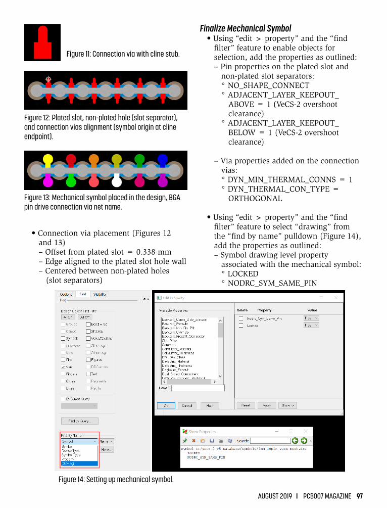
AUGUST 2019 I PCB007 MAGAZINE 97
• Connection via placement (Figures 12and 13)– Offset from plated slot = 0.338 mm– Edge aligned to the plated slot hole wall– Centered between non-plated holes
(slot separators)
Finalize Mechanical Symbol• Using “edit > property” and the “find
filter” feature to enable objects forselection, add the properties as outlined:– Pin properties on the plated slot and
non-plated slot separators:° NO_SHAPE_CONNECT° ADJACENT_LAYER_KEEPOUT_
ABOVE = 1 (VeCS-2 overshoot clearance) ° ADJACENT_LAYER_KEEPOUT_ BELOW = 1 (VeCS-2 overshoot clearance)
– Via properties added on the connectionvias:° DYN_MIN_THERMAL_CONNS = 1° DYN_THERMAL_CON_TYPE =
ORTHOGONAL
• Using “edit > property” and the “findfilter” feature to select “drawing” fromthe “find by name” pulldown (Figure 14),add the properties as outlined:– Symbol drawing level property
associated with the mechanical symbol:° LOCKED° NODRC_SYM_SAME_PIN
Figure 12: Plated slot, non-plated hole (slot separator), and connection vias alignment (symbol origin at cline endpoint).
Figure 13: Mechanical symbol placed in the design, BGA pin drive connection via net name.
Figure 11: Connection via with cline stub.
Figure 14: Setting up mechanical symbol.

98 PCB007 MAGAZINE I AUGUST 2019
Using VeCS Structure
Placing in Layout• Using “place > manually,” select
mechanical symbols for the filterpulldown (Figure 15) and place thesymbol in free space in the layout
• Enable “pins” in the “find filter” featureto select all of the pins on the placed VeCSstructure and “RMB > property edit”(Figure 16)
• Add the “NO_DRC” property to the pins(Figure 17)
• Now, freely copy the VeCS structureinside of the BGA pin field as required(Figure 18)
• Turn on the inner layers and route to viasalong the slot walls using “route >connect” (Figure 19)
Figure 15: The manual placement pulldown menu.
Figure 17: Adding the “NO_DRC” Property to the pins from the Edit Property diaglog box.
Figure 16: Accessing the properties to select all pins in the VeCS structure.
Figure 18: VeCS structures may now be freely copied in the design file.
Figure 19: inner layer routing along the slot walls.
Changing Layer Depth (VeCS-2)Using VeCS-2 structures requires a change in
the mechanical symbol and padstack to gener-ate the appropriate blind drills when structures is placed in the layout.
• Cross-section in symbol and padstack mustcontain the start/stop subclass names to

AUGUST 2019 I PCB007 MAGAZINE 99
identify the blind depth of the VeCS-2 structure
– It is not required to define the entirestackup; the start/stop subclass namesmust match the target design
• Padstack geometry definition on start/stoplayer drive the blind depth when placed inthe design
Setting Up Design Rules
PadstacksWith the advancements made in the 17.2
Padstack Editor, there are no special design rules required to successfully use a VeCS struc-ture in the layout.
• Plated slots: Adjacent layer keepout formechanical drill overshoot clearancefor VeCS-2
• Non-plated hole/slot (slot separator):Keepout on all layers for clearance tothe non-plated hole or slot– Utilizing by-layer keepouts and adjacent
layer keepouts for VeCS-2 structures
Pin Properties Applied in the LayoutPlacing the VeCS structure in the layout will
produce DRC errors between the plated slot and non-plated hole/slot (slot separator) pins, which is expected. To eliminate these DRC er-rors, the designer must apply NO_DRC prop-erties to the pins of the VeCS structure. This property can be added upon placing the first VeCS structure and a simple copy this struc-ture to all the required locations in the design.
Fabrication OutputVeCS structures in Allegro PCB design-
er should work directly out of the box ex-cept when moving to VeCS-2 structures (blind depth). To support VeCS-2, a manufacturing output change was made to generate the ap-propriate drill files for blind/buried drills and slots (Figures 20 and 21). This manufacturing output change was made in 17.2 QIR5 (S031) in December 2017. PCB007
Ed Hickey is product engineering director at Cadence Design Systems.
Mike Catrambone is senior principal product engineer at Cadence Design Systems.
Joan Tourné is CEO of NextGIn Technology BV.
Figure 20: Example of drill/route table.
Figure 21: 3D view of VeCS as solid and in cross-section.

100 PCB007 MAGAZINE I AUGUST 2019
Article by Nikolaus Schubkegel
Ultraviolet (UV) bump, also called UV cure, is a processing step in which the solder mask pattern is irradiated with ultraviolet and infra-red light. This step is performed with special equipment that is built as a continuous flow system. The system consists of a conveyor belt and tubular UV lamps mounted above and below the belt. The UV lamps (burners) are mounted under a hood. For safety reasons, it must be avoided that UV radiation penetrates outside because it is very dangerous for the human eye.
Typically, the light sources are powerful tu-bular mercury lamps with strong emissions in the UV and IR bands. It is an infrared-as-sisted UV exposure. UV radiation is desired, and infrared (IR) radiation is a needed side ef-fect. Generally, the light stays constant in the system; UV energy is adjusted by varying the transportation speed of the panels. The UV en-
ergy is selected in the range between 500–4,000 mJ (milijoules), depending on the solder mask and the purpose. The IR radiation will heat the PCB up to 60–70°C or more, depending on the selected UV energy and panel thickness.
Key Facts About UV Curing SystemsIn general, un-doped burners are used. Iron-
doped burners can also be used; then, less energy is needed. Almost all equipment is equipped with un-doped burners, which is his-torical. These types of equipment are used in many industries for curing of paints and inks. The un-doped lamps fit for almost all require-ments. On request, the un-doped burners can be replaced with doped burners. In the PCB in-dustry, iron-doped lamps are generally used; in other industries, it can also be gallium-doped lamps.
Depending on the solder mask (see later for further discussion), UV bump is performed either before final thermal cure or after final
Solder Mask Curing: UV Bump Overview

IPCEMERGINGENGINEER
ACCEPTING APPLICATIONS
IPC EMERGING ENGINEERS• Grow your technical knowledge and organizational skills with participation in IPC committees for development
of industry standards.• Build connections for technology interchange.• Become a valued contributor to the industry — like IPC Mentors.
BECOME AN IPC EMERGING ENGINEERIf you have worked in the industry less than 5 years or are a student in an engineering or engineering-related program at a College or University, and are ready to invest in your career.
You can commit to:
• Spending time with an Emerging Engineersharing experiences and providing guidance onIPC-related activities
• Attending IPC APEX EXPO for the next 3 years.• Helpingthenextgenerationbecometomorrow’s
standards development leaders.
Mentoring responsibilities include: participation in the candidate selectionprocess,briefingyourassignedIPCEmergingEngineerbefore and after meetings, making introductions to peers, participating in networking opportunities, and providing feedback to IPC twice each year.Send your professional biography and ideas for this program to: [email protected].
• Learning about new technologies and the industrystandards development process from subjectmatter experts
• Participating in IPC committee work on industrystandards development.
• Attending IPC APEX EXPO for the next 3 years.
Individuals selected as IPC Emerging Engineers will be awarded an All-Access Package to IPC APEX EXPO (approximately $1,500 value) to learn about all that IPC has to offer the industry.
Send your resumé to: [email protected].
IPC MENTORS• Develop your leadership skills by providing guidance to Emerging Engineers new to the industry, demonstrate
your technical and organizational expertise.• Expand your professional network.• Ensure that your IPC committee work continues.
JOIN THE IPC MENTORS TEAM If you have at least 7 years of industry experience, and have worked on an IPC committee for at least 5 years.
You can commit to:

102 PCB007 MAGAZINE I AUGUST 2019
thermal cure of the liquid photoimageable sol-der resist.
Energy Levels Required for UV CureGenerally, UV bump before the final ther-
mal cure is performed at a lower energy (500–2,000 mJ) in comparison to UV bump af-ter final thermal cure (1,500–4,000 mJ). UV bumping of flexible solder mask is carried out at much lower energy than for rigid products. And exposing the solder mask pattern on a contact exposing machine with a blank glass is not UV bump, even at extremely high ex-posing energy.
UV Cure Before the Final Thermal Cure As the solder mask heats to temperatures be-
yond the glass transition temperature (Tg) of that solder mask (the Tg of the solder mask after exposure and developing is lower and dif-ferent to the final Tg), the solder mask par-ticles will become movable. As the particles move, cross-linking continues, the remaining photoinitiator is destroyed, and volatile com-ponents (solvents) are blown out. Also, the surface hardness increases, and the volatile emissions reduce. Furthermore, condensation in the final cure oven is reduced. The chemi-cal resistance to different final finishes (e.g., immersion tin, ENIG, and HASL) and cleaning processes is improved. Moisture absorption is reduced. In short, after direct imaging, it con-tributes to sealing of the surface. The disad-vantage of UV bump before the final thermal cure is the risk of over cross-linking and em-brittlement. This happens if the energy is far higher than required and if the system is not closely monitored. The adhesion of legend ink and the adhesion of conformal coating might be reduced.
UV Cure After the Final Thermal CureThe temperature of the solder mask stays be-
low the Tg. The additional cross-linking can be neglected; the molecules swing only on fixed points, and the movement of the particles is limited. The remaining photoinitiator is de-stroyed and blown out. Residues condensed on the copper surface from the final curing
oven are being destroyed by photo-oxidation and oxidation with ozone. The remained vol-atiles are blown out; these volatiles might condense on copper and lead to plating defects in ENIG.
Moreover, the resistance to different final finishes is improved, and the absorption of moisture is reduced. Staining after HAL and after wave soldering is also reduced. The ionic contamination and the out-gassing improves significantly as well. And the adhesion of leg-end ink and conformal coating might be re-duced.
General AspectsUV bump performance, whether before ther-
mal cure or after, depends on following the curing recommendations of the solder mask brand/manufacturer. Not every solder mask requires UV bumping. There are LPI solder masks that generally require no UV bump (al-though a UV bump after thermal cure for such products does reduce the ionic contamination and out-gassing).
However, some products require UV bump-ing. In such cases, the technical datasheet will provide full instructions. There are also prod-ucts where UV bumping is optional either be-fore or after the final thermal cure.
Some solder mask manufacturers recom-mend UV bump before final thermal curing, while other manufacturers recommend UV bumping after final thermal curing. This de-pends on the product. Again, a complete and careful reading of the technical datasheet will disclose all product-specific instructions and cautions. This refers strictly to contact exposure. If exposure is done on a direct im-aging system, UV bump is helpful and rec-ommended.
In my opinion, UV bump before final ther-mal cure or afterwards is good in philosophy. In practice, sometimes it is not possible to fol-low the recommendations of the solder mask manufacturer due to the process chain and equipment alignment. Even if deviated from the recommendations of the solder mask man-ufacturer, I have no knowledge about defects that might occur.

AUGUST 2019 I PCB007 MAGAZINE 103
Things to Watch for During UV BumpIn some cases, UV bump might degrade the
adhesion of legend ink or conformal coating. This depends on the product formulation. Af-ter curing of the solder mask, you have active molecule centers left.
These active centers contribute to good ad-hesion of legend ink and conformal coating. During UV bump, these active centers are be-ing destroyed, giving bad adhesion. This phe-nomenon depends on the type of legend ink and conformal coating. Some products are more prone to adhesion loss than others.
To prevent wrinkling of solder mask between tracks at high copper height and high SM de-posit, UV bump before thermal cure is helpful and recommended. Staining of the solder mask after HASL can be prevented by giving boards a UV bump cure after the final thermal cure. This staining is caused by aggressive fluxes and washing the boards whilst still hot. This hap-pens mainly when exposure is direct imaging and is due to the missing wavelength of 200–350 nm. The solder mask surface is not sealed.
Direct Imaging If you process solder mask on contact-expos-
ing units with UV light-emitting diodes as the light source, or direct imaging systems with UV light-emitting diodes or UV laser-emitting di-odes, then consider UV bump before final ther-mal cure, as it improves the staining resistance to final finishes.
Other Applications UV bump is widely used in other applica-
tions as well. UV bump is also used for curing UV legend ink, UV solder mask, UV etch resist, UV gap filler, and UV hole filler. All of these products have been developed for UV curing. Thermal curing of these products is not pos-sible. Most solder mask manufacturers have such products in their portfolio. Apart from the PCB industry, UV bump is also used in other industries for curing of inks, paints, resins, etc. Some companies do not have UV bump and get along well without. But if UV bump is used and needed, the energy must be monitored very carefully because it drifts away. PCB007
References1. Technical datasheets from Taiyo, Huntsman, Sun
Chemical, and Lackwerke Peters.
Nikolaus Schubkegel retired in Feb-ruary 2019. For the past 12 years, Schubkegel worked at Umicore Gal-vanotechnik GmbH in Germany as a technical service engineer for Taiyo products. Before that, he worked as a process engineer in the solder mask
department at the former IBM-PCB plant (later STP) in Albstadt, Germany. Schubkegel obtained an M.Sc. degree in chemical engineering from the Polytechnic Institute in Timisoara.
Oak Ridge National Laboratory (ORNL) is training next-generation cameras called dynamic vision sensors (DVS) to interpret live in-formaion—a capability that has applications in robotics and could improve autonomous vehicle sensing.
Unlike a traditional digital camera, a DVS transmits per-pixel changes in light intensity. Individual pixel locations are recorded and time-stamped to the microsecond, creating data “events” that are processed by a neuromorphic network—a type of intelligent, energy-efficient computing architecture. This capability makes the sensors fast, power-efficient, and effective in wide ranges of light intensity.
“Because the DVS records only changes in what it sees, there is no redundant data,” said ORNL SULI intern Kemal Fidan.
(Source: ORNL)
‘Seeing’ in Real Time

104 PCB007 MAGAZINE I AUGUST 2019
1AWE 2019: Go XR, Be Awesome E
Dan Feinberg attended and covered the recent 2019 Augmented World Expo (AWE) and conference in Santa Clara, California. The event featured the lat-est developments and tech-nologies in augmented (AR), mixed (MR), virtual (VR), and extended virtual reality (many just call it all XR to make it simple). Here’s a wrap-up of the event.
2 Emma Hudson: From Tomboy to Tech Lead E
In this interview, Emma Hudson, CTO of Gen3, and Gayle Paterson, founder of Female Leaders in Tech, Everywhere (FLITE), dis-cuss careers and the elec-tronics industry.
3EPTE Newsletter: JPCA Show 2019, Part 2 E
Many new technolo-gies and products re-lated to flexible cir-cuits were introduced by mid-sized manu-facturers at the JPCA Show 2019. Oki Cable displayed several unique technologies that included stretchable and transparent circuits. They are proactive with introducing new materials for base materials as well as conductors and coverlay.
4Punching Out! Exit Planning 101 E
Proper planning can take away many headaches for the seller and buyer as well as increase the value of the company, help obtain better terms, and overall, make it easier to complete a transaction.
Editor Picks from PCB007
Dan Feinberg
Emma HudsonTom Kastner

AUGUST 2019 I PCB007 MAGAZINE 105
5Volunteers Honored for Contributions to IPC and the Electronics Industry E
IPC presented Committee Leadership, Special Recog-nition, and Distinguished Committee Service Awards at the recent SummerCom Standards Development Committee Meetings in Raleigh, North Carolina.
6N.A. PCB Sales and Orders Grow, but B2B Ratio Falls E
Total North Ameri-can PCB shipments in May 2019 were up 5.6% compared to the same month last year. Year-to-date sales growth as of May was 12.3%, and compared to the preceding month, shipments were up 2.5%.
7The PCB Norsemen: What Is Reliability Without Traceability? E
High reliability and compli-ance are hot topics at con-ferences all over the world. If you are a supplier to in-dustries like defense, auto-motive, medical, and aero-space/space, high-reliability and regulatory compliance are strict demands for electronic device manufacturers. This col-umn discusses how high-reliability demands enforce the need for traceability, and at what level the traceability should be.
8Dissecting the IPC Regional Survey on PCB Technology Trends E
Sharon Starr, Denny Fritz, and Mike Carano talk about the global 2018 IPC Technol-ogy Trends Report released early this year—the size of the survey, how it was con-ducted, the general findings, and regional differences. They also shared their takeaways and regional insights, and the industry outlook over the next five to 10 years.
9Kelvin Characterization to Accurately Predict Copper Thickness E
A few years ago at Integrated Test Corporation, we found that the reaction plan for void fallout at electrical test was ineffective and not standard-ized. Like many PCB manu-facturing facilities (including a Sanmina shop that Brandon Sherrieb used to work at), the reaction plan consisted of cross-section analysis to determine the void type.
JIt’s Only Common Sense: Five Tips for Rescuing Orphans E
It has happened to all of us. It’s part of doing business. No matter how hard you try, somewhere along the way, you lose a customer. These lost customers are what my friend Bruce appropriately dubbed “the orphans.” Here are five tips for rescuing orphans.
For the Latest PCB News and Information, Visit: PCB007.com
Brandon Sherrieb
Sharon Starr
Didrik Rech
Dan Beaulieu


AUGUST 2019 I PCB007 MAGAZINE 107
Career Opportunities
Senior Development Engineer
Rogers Corporation is seeking a senior develop-ment engineer accountable for the development of more complex products and processes, the estab-lishment of sound technical bases for these devel-opments, and effective interaction with technology, process, and platform innovation; operations; sales and marketing; and process engineering personnel to commercialize these developments.
Essential Functions:• Design and conduct experiments and interpret the results• Report on projects in both written and verbal formats at all levels of the organization• Perform technical troubleshooting of new products and processes; act as new product/ concept incubator for new technologies and platforms, identifying opportunities for improve- ment and incorporation design for manufacturing requirements resulting in a viable, scalable product• Provide ongoing process and manufacturing support to newly launched products as applicable• Provide support in terms of analytical equipment maintenance, methods development, material analysis, and documentation of new process or products• Manage capital projects for the purchase and installation of new process or support equipment; train employees in new processes Required Education and Experience:Ph.D., Ch.E., M.E., or material science, or B.S. or high-er in a technical discipline with accomplishment in product development and project management
Rogers Corporation provides equal employment oppor-tunities to minorities, females, veterans, and disabled
individuals as well as other protected groups.
OEM Sales ManagerChicago/Home-Office-Based
Want to advance your career by joining a globally successful and growing world-class CCL manufac-turer and help drive that success? We are seeking to hire an OEM sales manager to grow and manage key customer accounts with OEM’s and Tier 1 man-ufacturers in the USA, focusing on Ventec’s core market segments: mil/aero, automotive, and medi-cal, offering a full range of high-reliability materials, including polyimide, IMS, and thermal management products.
Skills and abilities required for the role:• Non-negotiable: Drive and tenacity!
Required:• 7 to 10 years’ experience in the PCB industry in engineering and/or manufacturing• Detail-oriented approach to tasks• Ability to manage tasks and set goals independently as well as part of a team• Knowledge of MS office products
Full product training will be provided.
This is a fantastic opportunity to become part of a successful brand and leading team with excellent benefits.
Please forward your resume to [email protected] and mention “Technical Sales Engineer—Chicago”
in the subject line.

108 PCB007 MAGAZINE I AUGUST 2019
Career Opportunities
Gardien Is Hiring!The Gardien Group, a leading solutions
provider in the PCB industry, is looking to fill multiple openings in their China, Japan, Tai-wan, and United States service centers.
We are looking for electrical engineers, operations managers, machine operators, and sales executives. Prior experience in the PCB industry is beneficial but not es-sential. Training will be provided along with excellent growth opportunities, a benefits package, and periodic bonuses.
Our global teams are from diverse cul-tures and work cohesively as a tight-knit unit. With performance and initiative, there are plenty of opportunities for professional growth.
Gardien is an equal opportunity employ-er. Employment decisions are made without any regard to race, color, religion, national or ethnic origin, gender, sexual orientation, age, disability, or other characteristics.
Interested candidates, please contact us with your resume and a cover letter. Kindly note that only shortlisted candidate will be contacted.
Apply at [email protected].
Field Service Engineer (Location Negotiable)
Are you passionate about delivering an excep-tional user experience? Come work as a field ser-vice engineer at the industry’s leading inspection company that offers great benefits with opportu-nities to advance while learning alongside accom-plished business leaders.
The Company: Koh Young is the leading 3D inspection solutions provider in the electronics manufacturing industry. With is new offices in At-lanta and Guadalajara, it helps its customers opti-mize their printed circuit board assembly process.
The Position: Deliver technical services—in-cluding installation, support, and maintenance—to elevate the user experience. Location is flexible, but OH, IN, IL, MA, MI, FL, CA, or Toronto are desired.
The Reasons: An opportunity to apply lead-ing-edge inspection technology to products you know and use every day. A great environment that supports its team and treats everyone like family.
Join the industry’s leading provider of true 3D inspection solutions
Interested? Submit your resume below.

AUGUST 2019 I PCB007 MAGAZINE 109
Career Opportunities
Become a Certified IPC Master Instructor
Opportunities are available in Canada, New Eng-land, California, and Chicago. If you love teaching people, choosing the classes and times you want to work, and basically being your own boss, this may be the career for you. EPTAC Corporation is the lead-ing provider of electronics training and IPC certifi-cation and we are looking for instructors that have a passion for working with people to develop their skills and knowledge. If you have a background in electronics manufacturing and enthusiasm for education, drop us a line or send us your resume. We would love to chat with you. Ability to travel re-quired. IPC-7711/7721 or IPC-A-620 CIT certification a big plus.
Qualifications and skills• A love of teaching and enthusiasm to help others learn • Background in electronics manufacturing• Soldering and/or electronics/cable assembly experience• IPC certification a plus, but will certify the right candidate
Benefits• Ability to operate from home. No required in-office schedule• Flexible schedule. Control your own schedule• IRA retirement matching contributions after one year of service• Training and certifications provided and maintained by EPTAC
Key Account Managers/Outside Sales
Itasca, IL • Hampstead, NH • Ontario, CA
NCAB Group is a global leader in the printed circuit board (PCB) industry, selling over 110 million PCBs yearly from 14 different countries. We are now look-ing for key account managers for our U.S. teams.
We are looking for sales professionals with at least five years of printed circuit board experience and/or semiconductor experience and knowledge. This is a sales position that requires your ability to convert those cold calls into high-value customer meetings.
What we are looking for:• A “hunter” mentality• The ability to create solid customer relationships• A strong history of working closely with your inside sales teams• An excellent ability presenting your product and doing the deep dive during your customer visit to identify your customers’ pain points• Knowledge of “SPIN” selling• A college degree preferred but not required• Someone who enjoys travel both domestically and globally
Who are we? At NCAB Group, it is the people that make us unique. We work according to our values; quality first, strong relationships and full responsi-bility, and encourage employee empowerment and initiatives.

110 PCB007 MAGAZINE I AUGUST 2019
Career Opportunities
Development ChemistCarson City, NV
Develop new products and modify existing products as identified by the sales staff and company manage-ment. Conduct laboratory evaluations and tests of the industry’s products and processes. Prepare detailed written reports regarding chemical characteristics. The development chemist will also have supervisory responsibility for R&D technicians.
Essential Duties:• Prepare design of experiments (DOE) to aid in the development of new products related to the solar energy industry, printed electronics, inkjet technolo- gies, specialty coatings and additives, and nano- technologies and applications• Compile feasibility studies for bringing new products and emerging technologies through manufacturing to the marketplace• Provide product and manufacturing support• Provide product quality control and support• Must comply with all OSHA and company workplace safety requirements at all times• Participate in multifunctional teams
Required Education/Experience:• Minimum 4-year college degree in engineering or chemistry• Preferred: 5–10 years of work experience in designing 3D and inkjet materials, radiation cured chemical technologies, and polymer science• Knowledge of advanced materials and emerging technologies, including nanotechnologies
Working Conditions:• Chemical laboratory environment• Occasional weekend or overtime work• Travel may be required
Assistant Department Manager, Operations, Carson City, NV
This is an entry-level professional management trainee position. Upon completion of a 1–2-year ap-prenticeship, this position will be elevated to facility/operations manager. Primary functions during training: shadow incumbent staff managers to learn and under-stand the operations and personnel of the operations department. This position will train and learn, develop, implement, and coordinate strategies related directly to the manufacture of Taiyo products. Additionally, this position will be learning all about the facility, environ-ment, and health and safety functions. Eventually, this position will be responsible for the administration, se-curity and maintenance of the facility and warehouse
Required Experience/Education:• 4-year college degree in industrial engineering or another similar science discipline combined with work experience in ink or coatings manufacturing• Ability to read, analyze, and interpret common scientific and technical journals, financial reports, and legal documents• Ability to respond to inquiries or complaints from customers, regulatory agencies, or members of the business community• Ability to develop and implement goals, objectives, and strategies• Ability to effectively present information to top man- agement, public groups, and/or boards of directors• Ability to apply principles of logical or scientific thinking to a wide range of intellectual and practical problems• Knowledge of governmental safety, environmental, transportation regulations/laws
Preferred Skills/Experience:• Bilingual (Japanese/English)• Toyota Production System (TPS)
Working Conditions:• Occasional weekend or overtime work
See complete job listing for more information.
AUGUST 2019 I PCB007 MAGAZINE 111
Career Opportunities
Analyst Programmer, Hong Kong
We believe in caring about our people because they are our greatest asset. CML works with mul-ticultural stakeholders daily to achieve more and bring them the best solutions. That’s why we con-tinuously invest in optimizing our culture and focus on providing our team with opportunities to develop their skills (e.g., through professional coaching to achieve their highest potential).
The analyst programmer will assist the IT and ERP manager in Hong Kong to support the company’s BI systems, ERP systems, and other related IT-land-scape applications.
In addition, this post will participate in system de-velopment projects and provide support including, but not limited to, user requirement collection and analysis, user training, system documentation, sys-tem support and maintenance, enhancement, and programming. • Develop and enhance related IT systems and applications• Prepare functional specifications• Transfer the relevant business and interface processes into IT systems and other applications to get a maximum automation degree and prepare all required business reports• Conduct function testing and prepare documentation• Manage help desk/hotline service CML is a leading provider of printed circuit boards. We develop tailor-made sourcing and manufacturing solutions for our customers worldwide with strong partnerships and reliable connections.
Technical Account ManagerChicago/Minneapolis
Insulectro, the largest national distributor of printed circuit board materials, is seeking a talent-ed sales superstar for a Technical Account Manager role based out of either our Chicago or Minneapolis office. This role will focus on maintaining the exist-ing customer base and developing new business within the assigned territory in both the printed cir-cuit board and printed electronics industries. We are looking for the perfect fit of education, experience, and attitude that matches our company culture and enhances the service level to our customers.
Qualifications:• A self-motivated business professional who is driven to succeed with a minimum of 3 years outside sales experience in the PCB or PE industry• Proven sales/business development record• Excellent communication and interpersonal skills• OEM and electronic assembly experience is a plus
We offer:• Competitive salary and commission plan with a comprehensive benefits package• A fun, high-energy company with an entrepreneurial spirit• A great group of people to work with!

112 PCB007 MAGAZINE I AUGUST 2019
Career Opportunities
Technical Sales Engineer San Jose, CA, USA
The technical sales engineer will perform technical audits and help customers troubleshoot and opti-mize their solder mask process, prepare and deliver technical presentations explaining products or ser-vices to customers and prospective customers, col-laborate with sales teams to understand customer requirements and provide sales support, secure and renew orders and arrange delivery, and help in re-searching and developing new products.
Required Education/Experience:Applicants must have good “hands-on” knowledge of the printed circuit board (PCB) industry and the liquid photo imageable (LPI) solder mask process. Candidates must be self-motivated, capable of man-aging key accounts and developing new business opportunities that generate new sales.
• College degree preferred with solid knowledge of chemistry• 3–5 years of work experience in a technical role within the PCB industry• 3–5 years of work experience in a sales role• Computer knowledge, Microsoft Office environment• Good interpersonal relationship skills• Good English verbal and written skills are necessary
Working Conditions:Occasional weekend or overtime work. Travel may be 25–50% or greater.
APCT, Printed Circuit Board Solutions:
Opportunities AwaitAPCT, a leading manufacturer of print-
ed circuit boards, has experienced rapid growth over the past year and has multiple opportunities for highly skilled individuals looking to join a progressive and growing company. APCT is always eager to speak with professionals who understand the val-ue of hard work, quality craftsmanship, and being part of a culture that not only serves the customer but one another.
APCT currently has opportunities in Santa Clara, CA; Orange County, CA; Anaheim, CA; Wallingford, CT; and Austin, TX. Positions available range from manufacturing to qual-ity control, sales, and finance.
We invite you to read about APCT at APCT.com and encourage you to understand our core values of passion, commitment, and trust. If you can embrace these principles and what they entail, then you may be a great match to join our team! Peruse the op-portunities by clicking the link below.
Thank you, and we look forward to hearing from you soon.

AUGUST 2019 I PCB007 MAGAZINE 113
Service Engineer Reflow Soldering Systems (m/f)
To strengthen our service team at Rehm Thermal Systems LLC. in Roswell, Georgia, we are seeking candidates to fill the position of Service Engineer— Reflow Soldering Systems.
Your area of responsibility:• Installation of Rehm reflow soldering systems at the customers’ site• Maintenance and repair work as well as technical service for our customers in the USA and Mexico• Execution of machine training
Your profile:• Completed education studies as an engineer in the field of electrical engineering/mechatronics or comparable education (m/f)• Basic and specialist knowledge in the field of electronics and electrical engineering/ mechatronics• High willingness to travel and have flexible employment• Service-oriented and like to work independently
We offer:• Performance-oriented, attractive compensation• Comprehensive training• A safe workplace in one successful group of companies• Self-responsibility and leeway
Please send application documents online to Natalie Werner at [email protected].
Career Opportunities
Multiple Positions Available
The Indium Corporation believes that materials science changes the world. As leaders in the electronics assembly in-dustry we are seeking thought leaders that are well-qualified to join our dynam-ic global team.
Indium Corporation offers a diverse range of career opportunities, including:
• Maintenance and skilled trades • Engineering• Marketing and sales • Finance and accounting• Machine operators and production • Research and development• Operations
For full job description and other immediate openings in a number
of departments:
www.indium.com/jobs

114 PCB007 MAGAZINE I AUGUST 2019
Sales Representatives (Specific Territories)
Escondido-based printed circuit fabricator U.S. Circuit is looking to hire sales representatives in the following territories:
• Florida• Denver• Washington• Los Angeles
Experience:
• Candidates must have previous PCB sales experience.
Compensation: • 7% commission
Contact Mike Fariba for
more information.
Career Opportunities
SMT Field Technician Huntingdon Valley, PA
Manncorp, a leader in the electronics assembly industry, is looking for an additional SMT Field Tech-nician to join our existing East Coast team and in-stall and support our wide array of SMT equipment.
Duties and Responsibilities:• Manage on-site equipment installation and customer training • Provide post-installation service and support, including troubleshooting and diagnosing techni- cal problems by phone, email, or on-site visit• Assist with demonstrations of equipment to potential customers• Build and maintain positive relationships with customers• Participate in the ongoing development and improvement of both our machines and the customer experience we offer
Requirements and Qualifications:• Prior experience with SMT equipment, or equivalent technical degree • Proven strong mechanical and electrical troubleshooting skills• Proficiency in reading and verifying electrical, pneumatic, and mechanical schematics/drawings• Travel and overnight stays• Ability to arrange and schedule service trips
We Offer:• Health and dental insurance• Retirement fund matching • Continuing training as the industry develops

AUGUST 2019 I PCB007 MAGAZINE 115
We Are Recruiting! A fantastic opportunity has arisen with-in Electrolube, a progressive global electro-chemicals manufacturer. This prestigious new role is for a sales development manag-er with a strong technical sales background (electro-chemicals industry desirable) and great commercial awareness. The key focus of this role is to increase profitable sales of the Electrolube brand within the Midwest area of the United States; this is to be achieved via a strategic program of major account devel-opment and progression of new accounts/projects. Monitoring of competitor activity and recognition of new opportunities are also integral to this challenging role. Full product training to be provided. The successful candidate will benefit from a generous package and report directly to the U.S. general manager.
Applicants should apply with their CV to [email protected]
(agencies welcome)
Career Opportunities
Zentech Manufacturing:
Hiring Multiple PositionsAre you looking to excel in your career and
grow professionally in a thriving business? Zentech, established in Baltimore, Maryland, in 1998, has proven to be one of the premier electronics contract manufacturers in the U.S.
Zentech is rapidly growing and seeking to add Manufacturing Engineers, Program Managers, and Sr. Test Technicians. Offer-ing an excellent benefit package including health/dental insurance and an employer-matched 401k program, Zentech holds the ultimate set of certifications relating to the manufacture of mission-critical printed cir-cuit card assemblies, including: ISO:9001, AS9100, DD2345, and ISO 13485.
Zentech is an IPC Trusted Source QML and ITAR registered. U.S. citizens only need apply.
Please email resume below.

116 PCB007 MAGAZINE I AUGUST 2019
IPC Master Instructor
This position is responsible for IPC and
skill-based instruction and certification
at the training center as well as train-
ing events as assigned by company’s
sales/operations VP. This position may
be part-time, full-time, and/or an inde-
pendent contractor, depending upon
the demand and the individual’s situa-
tion. Must have the ability to work with
little or no supervision and make appro-
priate and professional decisions. Can-
didate must have the ability to collab-
orate with the client managers to con-
tinually enhance the training program.
Position is responsible for validating
the program value and its overall suc-
cess. Candidate will be trained/certified
and recognized by IPC as a Master In-
structor. Position requires the input and
management of the training records.
Will require some travel to client’s facili-
ties and other training centers.
For more information, click below.
Career Opportunities
YOURJOBAD
HEREFor information, please contact:
BARB [email protected]
+1 916.608.0660 (-7 GMT)

118 PCB007 MAGAZINE I AUGUST 2019
Coming Soon to PCB007 Magazine:SEPTEMBER: StandardsWe report on recent developments in current and emerging standards and take a step back to discuss some of the inherent strengths and weaknesses of standards processes.
OCTOBER: Landscape of the IndustryWe examine the current landscape of the electronics industry and how it is changing from design tools to AI, manufacturing, and markets.
Events Calendar
Additional Event Calendars
NEPCON South China 2019 EAugust 28–30, 2019Shenzhen, China
C3Bio Conference on Biosensors, Bioelectronics, and Biodevices ESeptember 9–10, 2019Bath, U.K.
C3Bio Training Workshop on Lab-on-Chip ESeptember 11–12, 2019Bath, U.K.
EIPC PCB Pavilion @ WNIE Exhibition ESeptember 18–19, 2019 Warwickshire, U.K.
productronica India 2019 ESeptember 25–27, 2019Delhi NCR, India
electronica India 2019 ESeptember 25–27, 2019Delhi NCR, India
52nd International Symposium on Microelectronics ESeptember 29–October 3, 2019Boston, Massachusetts, USA
IPC Electronics Materials Forum ENovember 5–7, 2019Minneapolis, Minnesota, USA
productronica 2019 ENovember 12–15, 2019Munich, Germany
2019 International Electronics Circuit Exhibition (Shenzhen) EDecember 4–6, 2019Shenzhen, China

AUGUST 2019 I PCB007 MAGAZINE 119
ADVERT ISER INDEXPUBLISHER: BARRY MATTIES [email protected]
SALES MANAGER: BARB HOCKADAY (916) 608-0660; [email protected]
SALES: ANGELA ALEXANDER(408) 489-8389; [email protected]
MARKETING SERVICES: TOBEY MARSICOVETERE (916) 266-9160; [email protected]
MANAGING EDITOR: NOLAN JOHNSON (503) 597-8037; [email protected]
CONTRIBUTING EDITOR: PATRICIA GOLDMAN (724) 299-8633; [email protected]
CONTRIBUTING TECHNICAL EDITOR: DAN [email protected]
TECHNICAL EDITOR: PETE STARKEY+44 (0) 1455 293333; [email protected]
ASSOCIATE EDITOR: KIERSTEN [email protected]
CONTRIBUTING TECHNICAL EDITOR: HAPPY HOLDEN(616) 741-9213; [email protected]
PRODUCTION MANAGER: SHELLY STEIN [email protected]
MAGAZINE LAYOUT: RON MEOGROSSI
AD DESIGN: SHELLY STEIN, MIKE RADOGNA, TOBEY MARSICOVETERE
INNOVATIVE TECHNOLOGY: BRYSON MATTIES
COVER: SHELLY STEIN
PCB007 MAGAZINE®
is published by BR Publishing, Inc., 942 Windemere Dr. NW, Salem, OR 97304
© 2019 BR Publishing, Inc. does not assume and hereby disclaims any liability to any person for loss
or damage caused by errors or omissions in the material contained within this publication, regardless
of whether such errors or omissions are caused accidentally, from negligence or any other cause.
August 2019, Volume 9, Number 8PCB007 MAGAZINE is published monthly,
by BR Publishing, Inc.
atg Luther & Maelzer GmbH................................. 71
Burkle North America............................................ 41
Chemcut.................................................................. 29
DB Management.................................................... 33
Electra Polymers.................................................... 91
Entelechy Global.................................................... 61
ESI.............................................................................. 77
Eternal Technology Corporation......................... 5
Excellon.................................................................... 21
Fein-line Associates............................................. 95
Gardien..................................................................... 37
I-Connect007 eBooks................................ 2, 3, 117
IPC...................................................................... 27, 101
Ludy............................................................................. 7
Mentor, a Siemens Business............................. 25
MivaTek Global...................................................... 49
Nordson March...................................................... 45
Orbotech.................................................................. 65
Panasonic Electronic Materials......................... 15
Atotech .................................................................... 85
Pluritec..................................................................... 57
Prototron Circuits.................................................. 53
Rogers Corporation.............................................. 89
Taiyo America........................................................... 11
Technica USA......................................................... 35
Ucamco..................................................................... 81
Ventec International Group................................ 73
Viking Test................................................................ 17

www.iconnect007.com
myiconnect007.com mediakit.iconnect007.comEDITORIAL CONTACT
Nolan [email protected]+1 503 597-8037 GMT-7
SALES CONTACT
Barb [email protected]+1 916 365-1727 GMT-7
FREE SUBSCRIPTION