Packaging of Bio-MEMS: Strategies, Technologies, and Applications
14
IEEE TRANSACTIONS ON ADVANCED PACKAGING, VOL. 28, NO. 4, NOVEMBER 2005 533 Packaging of Bio-MEMS: Strategies, Technologies, and Applications Thomas Velten, Hans Heinrich Ruf, David Barrow, Nikos Aspragathos, Panagiotis Lazarou, Erik Jung, Member, IEEE, Chantal Khan Malek, Martin Richter, Jürgen Kruckow, Associate Member, IEEE, and Martin Wackerle Abstract—Biomicroelectromechanical systems (bio-MEMS) are MEMS which are designed for medical or biological applications. As with other MEMS, bio-MEMS frequently, have to be pack- aged to provide an interface to the macroscale world of the user. Bio-MEMS can be roughly divided in two groups. Bio-MEMS can be pure technical systems applied in a biological environ- ment or technical systems which integrate biological materials as one functional component of the system. In both cases, the materials which have intimate contact to biological matter have to be biocompatible to avoid unintentional effects on the biological substances, which in case of medical implants, could harm the patient. In the case of biosensors, the use of nonbiocompatible materials could interfere with the biological subcomponents which would affect the sensor’s performance. Bio-MEMS containing biological subcomponents require the use of “biocompatible” technologies for assembly and packaging; e.g., high temperatures occurring, for instance, during thermosonic wire bonding and other thermobonding processes would denature the bioaffinity layers on biosensor chips. This means that the use of selected or alternative packaging and assembly methods, or new strategies, is necessary for a wide range of bio-MEMS applications. This paper provides an overview of some of the strategies, technologies, and applications in the field of bio-MEMS packaging. It includes the following: • strategies for the partitioning of subsystems within integrated microsystems for (bio)chemical analysis/synthesis; • methods for microassembly of bio-MEMS; • technologies for bonding of polymer bio-MEMS components; • packaging of miniature medical devices; • packaging of biosensors for in vitro applications; • packaging of micropumps as a bio-MEMS component. The applications discussed are derived from different fields to demonstrate the plethora of bio-MEMS considerations. In com- mercial production, packaging is possibly the major cost factor of bio-MEMS-based products, and its development requires special attention. Manuscript received November 2, 2004; revised July 25, 2005. This work was supported by the European Union under Grant EU IST-2000-28214 for the packaging of the BIOMIC chip. T. Velten and H. H. Ruf are with the Fraunhofer Institute for Biomedical Engineering (IBMT), 66386 St. Ingbert, Germany (e-mail: thomas.velten@ ibmt.fraunhofer.de). D. Barrow is with the Cardiff School of Engineering, Cardiff University, Cardiff CF24 3TF, U.K. (e-mail: [email protected]). N. Aspragathos and P. Lazarou are with the Robotics Group Mechanical and Aeronautics Engineering Department, University of Patras, 26500 Rion, Greece (e-mail: [email protected]). E. Jung is with the Fraunhofer Institute for Reliability and Microintegration (IZM), 13355 Berlin, Germany (e-mail: [email protected]). C. K. Malek is with the Laboratoire Franche-Comté Electronique Mécanique Thermique Optique-Sciences et Technologies (FEMTO-ST) UMR CNRS, 25044 Besançon, France (e-mail: [email protected]). M. Richter, J. Kruckow, and M. Wackerle are with the Fraunhofer Institute for Reliability and Microintegration (IZM), 80686 Munich, Germany (e-mail: [email protected]). Digital Object Identifier 10.1109/TADVP.2005.858427 Index Terms—Biomicroelectromechanical systems (bio-MEMS), bioaffinity, biosensor, gluing, joining, microsystems, point-of-care testing, wire-bonding. I. INTRODUCTION M EMS for biological or medical applications or involving biological component(s), so-called biomicroelectrome- chanical systems (bio-MEMS) [1] are becoming more and more popular. Depending on their applications, this is justified by the inherent benefits of miniaturization in bio-MEMS such as small size, low weight, potential low unit costs per device, ef- ficient transduction processes, high reaction rate, low reagent consumption, and the potential to manufacture minimally inva- sive devices and systems. A prominent medical application for bio-MEMS is the field of medical implants such as pacemakers, hearing aids and drug- eluting implants to name a few. It is obvious that miniaturiza- tion is a key desirable requirement for implantable devices. This is especially true for implants in very small organs or those which are inserted using minimally invasive surgical procedures where the maximum allowable size is restricted by the diameter of the working channel in an endoscope. Medical implants are often rather complex systems and can consist of many compo- nents such as power sources, transducers, control units, modules for wireless communication, etc., potentially resulting in rather bulky devices if inappropriate packaging technologies are used. Example packaging technologies suitable for miniaturized and high-density bio-MEMS includes bare die assembly techniques like flip-chip technology. These, provide thin, small, and light- weight features and can be implemented on a multitude of sub- strates such as ceramic, laminate, molded interconnect devices (MID) as well as on flexible substrates. Very often, these pro- cesses use materials which are not biocompatible. In this case, additional encapsulation steps are necessary to avoid a direct contact between nonbiocompatible materials and body fluids or tissue. Another bio-MEMS category comprises biosensors or com- plete lab-on-a-chip systems for analytical tasks [2]. Biochips and biosensors are regarded as key elements for the development of multianalyte detecting instruments, especially of hand-held instruments for point-of-care or point-of-use testing. Compared to conventional microelectronic chips, chemosensing biochips additionally require the controlled mass transfer, i.e., the access of analytes and reagents to the biosensing surfaces of the chip. On the other hand, interferences by chemical compounds on the detection mechanism and the transducing elements of the sensor 1521-3323/$20.00 © 2005 IEEE Authorized licensed use limited to: Lancaster University Library. Downloaded on December 2, 2009 at 11:25 from IEEE Xplore. Restrictions apply.
Transcript of Packaging of Bio-MEMS: Strategies, Technologies, and Applications
IEEE TRANSACTIONS ON ADVANCED PACKAGING, VOL. 28, NO. 4, NOVEMBER 2005 533
Packaging of Bio-MEMS: Strategies, Technologies,and Applications
Thomas Velten, Hans Heinrich Ruf, David Barrow, Nikos Aspragathos, Panagiotis Lazarou, Erik Jung, Member, IEEE,Chantal Khan Malek, Martin Richter, Jürgen Kruckow, Associate Member, IEEE, and Martin Wackerle
Abstract—Biomicroelectromechanical systems (bio-MEMS) areMEMS which are designed for medical or biological applications.As with other MEMS, bio-MEMS frequently, have to be pack-aged to provide an interface to the macroscale world of the user.Bio-MEMS can be roughly divided in two groups. Bio-MEMScan be pure technical systems applied in a biological environ-ment or technical systems which integrate biological materialsas one functional component of the system. In both cases, thematerials which have intimate contact to biological matter have tobe biocompatible to avoid unintentional effects on the biologicalsubstances, which in case of medical implants, could harm thepatient. In the case of biosensors, the use of nonbiocompatiblematerials could interfere with the biological subcomponents whichwould affect the sensor’s performance. Bio-MEMS containingbiological subcomponents require the use of “biocompatible”technologies for assembly and packaging; e.g., high temperaturesoccurring, for instance, during thermosonic wire bonding andother thermobonding processes would denature the bioaffinitylayers on biosensor chips. This means that the use of selected oralternative packaging and assembly methods, or new strategies, isnecessary for a wide range of bio-MEMS applications. This paperprovides an overview of some of the strategies, technologies, andapplications in the field of bio-MEMS packaging. It includes thefollowing:
• strategies for the partitioning of subsystems within integratedmicrosystems for (bio)chemical analysis/synthesis;
• methods for microassembly of bio-MEMS;• technologies for bonding of polymer bio-MEMS components;• packaging of miniature medical devices;• packaging of biosensors for in vitro applications;• packaging of micropumps as a bio-MEMS component.
The applications discussed are derived from different fields todemonstrate the plethora of bio-MEMS considerations. In com-mercial production, packaging is possibly the major cost factor ofbio-MEMS-based products, and its development requires specialattention.
Manuscript received November 2, 2004; revised July 25, 2005. This workwas supported by the European Union under Grant EU IST-2000-28214 for thepackaging of the BIOMIC chip.
T. Velten and H. H. Ruf are with the Fraunhofer Institute for BiomedicalEngineering (IBMT), 66386 St. Ingbert, Germany (e-mail: [email protected]).
D. Barrow is with the Cardiff School of Engineering, Cardiff University,Cardiff CF24 3TF, U.K. (e-mail: [email protected]).
N. Aspragathos and P. Lazarou are with the Robotics Group Mechanical andAeronautics Engineering Department, University of Patras, 26500 Rion, Greece(e-mail: [email protected]).
E. Jung is with the Fraunhofer Institute for Reliability and Microintegration(IZM), 13355 Berlin, Germany (e-mail: [email protected]).
C. K. Malek is with the Laboratoire Franche-Comté Electronique MécaniqueThermique Optique-Sciences et Technologies (FEMTO-ST) UMR CNRS,25044 Besançon, France (e-mail: [email protected]).
M. Richter, J. Kruckow, and M. Wackerle are with the Fraunhofer Institutefor Reliability and Microintegration (IZM), 80686 Munich, Germany (e-mail:[email protected]).
Digital Object Identifier 10.1109/TADVP.2005.858427
Index Terms—Biomicroelectromechanical systems (bio-MEMS),bioaffinity, biosensor, gluing, joining, microsystems, point-of-caretesting, wire-bonding.
I. INTRODUCTION
MEMS for biological or medical applications or involvingbiological component(s), so-called biomicroelectrome-
chanical systems (bio-MEMS) [1] are becoming more and morepopular. Depending on their applications, this is justified bythe inherent benefits of miniaturization in bio-MEMS such assmall size, low weight, potential low unit costs per device, ef-ficient transduction processes, high reaction rate, low reagentconsumption, and the potential to manufacture minimally inva-sive devices and systems.
A prominent medical application for bio-MEMS is the fieldof medical implants such as pacemakers, hearing aids and drug-eluting implants to name a few. It is obvious that miniaturiza-tion is a key desirable requirement for implantable devices. Thisis especially true for implants in very small organs or thosewhich are inserted using minimally invasive surgical procedureswhere the maximum allowable size is restricted by the diameterof the working channel in an endoscope. Medical implants areoften rather complex systems and can consist of many compo-nents such as power sources, transducers, control units, modulesfor wireless communication, etc., potentially resulting in ratherbulky devices if inappropriate packaging technologies are used.Example packaging technologies suitable for miniaturized andhigh-density bio-MEMS includes bare die assembly techniqueslike flip-chip technology. These, provide thin, small, and light-weight features and can be implemented on a multitude of sub-strates such as ceramic, laminate, molded interconnect devices(MID) as well as on flexible substrates. Very often, these pro-cesses use materials which are not biocompatible. In this case,additional encapsulation steps are necessary to avoid a directcontact between nonbiocompatible materials and body fluids ortissue.
Another bio-MEMS category comprises biosensors or com-plete lab-on-a-chip systems for analytical tasks [2]. Biochipsand biosensors are regarded as key elements for the developmentof multianalyte detecting instruments, especially of hand-heldinstruments for point-of-care or point-of-use testing. Comparedto conventional microelectronic chips, chemosensing biochipsadditionally require the controlled mass transfer, i.e., the accessof analytes and reagents to the biosensing surfaces of the chip.On the other hand, interferences by chemical compounds on thedetection mechanism and the transducing elements of the sensor
1521-3323/$20.00 © 2005 IEEE
Authorized licensed use limited to: Lancaster University Library. Downloaded on December 2, 2009 at 11:25 from IEEE Xplore. Restrictions apply.
534 IEEE TRANSACTIONS ON ADVANCED PACKAGING, VOL. 28, NO. 4, NOVEMBER 2005
have to be avoided. This requirement can present a considerablechallenge in developing and packaging miniaturized biosensorarrays where a close integration of molecular recognition andtransducer elements is attempted for efficient signal transfer andsensitive detection. Only biochip-compatible packaging tech-niques are suited for these devices, i.e., techniques which do notdenature the bioaffinity sensor layers already on the biochips tobe packaged. This limits the temperatures to be used as wellas other physical and chemical treatments. Most proteins, forexample, denature above 40 C. However, some, such as de-oxyribonucleic acid (DNA) can withstand temperatures of upto about 100 C. Both mentioned biomaterials are usually notcompatible with plasma treatment and organic solvents.
Not only the choice of appropriate materials and packagingtechnologies but also the packaging strategy is of high im-portance regarding the lifetime, product volume, and costs.Packaging strategy comprises the partitioning, e.g., the divisionof bio-MEMS in functional subsystems, the selection of com-patible processes and the planning of a fabrication workflowwhich would produce the least interference between biologicalcomponent and technical process. Analytical bio-MEMS forinstance usually consist of several subunits for sample acqui-sition, sample preparation, sensing, data analysis, etc. Themanufacturer must choose the degree of integration (mono-lithic, hybrid, discrete subsystems) and to make the divisionin disposable and durable subsystems. Another strategic de-cision is to either use biocompatible packaging methods or toencapsulate conventionally packaged parts of the bio-MEMSwith a biocompatible material. An example for the selection ofa biochip-compatible process is wedge-wedge wire-bondingwhich can be done at room temperature whereas ball-wedgebonding requires elevated temperatures which are not toleratedby biomolecules. Regarding the workflow, it is wise to planthe integration of the biological component as late as possiblein the sequence of fabrication steps so as to avoid bioincom-patibilities. However, other processing operations may placeoverriding requirements; for instance, it might be impossibleto deposit an array of bioaffinity layers in a biochip after thecover-plate has been bonded on a microfluidic system.
Another important aspect of packaging addressed in thispaper is microassembly, comprising precise positioning, ori-entating, joining, and assembling techniques. Assembly is ofutmost importance for bio-MEMS as they are often composedof various subcomponents fabricated on independent processlines and being made of different materials. An example shownbelow is the assembly of a polymer microfluidic module to a sil-icon biochip. The general goal is to achieve hybrid microscaledevices of high complexity, while maintaining high yield andlow cost. Additional aspects of the final system that can beintegrated while performing the packaging process may resultin higher level of functionality (e.g., thermal insulation, controlof particle or media ingress), without adding significantly tothe system cost. The lack of flexibility and adaptability of mostcurrent assembling systems known from nonbio-MEMS (oftenmade of silicon) to other kinds of materials and processesmakes it necessary to apply alternative joining technologies.Some of the joining techniques commonly used for bio-MEMSwill be presented.
This review will discuss first the strategies for partitioningsubsystems within an integrated microsystem. These are theprimary considerations when commencing a system design.Sections II-B and II-C are purely technically oriented andreport on methods for microassembly as well as on varioustechnologies for joining polymer bio-MEMS components.Section II-D focuses on appropriate electrical assembly andinterconnection techniques. Several applications are presented.In Sections II-E and II-F, two successful packaging examplesfor bio-MEMS—an in vitro biosensor and a piezoelectricmicropump—are presented in more detail.
II. STRATEGIES, TECHNOLOGIES, AND APPLICATIONS
A. Bio-MEMS Subsystems Partitioning Strategies
1) Material Trends: Bio-MEMS defines a diversity of mi-crosystems functional embodiments. This diversity continuesto expand as applications in different industrial sectors aredeveloped [1]. One important domain of these developmentsis led by the miniaturization of systems for (bio)chemical andmolecular analysis/synthesis [2]. This is driven by manifoldreasons such as mass, volume, performance, and ergonomicsconsiderations. Such multifunctional devices and systemsmay incorporate (bio)chemical, biological, electromagnetic,electronic, fluidic, and mechanical functionalities. Further-more, they are truly three-dimensional (3-D), micro- andnanostructured and moving toward reconfigurable capability.Accordingly, to meet these diverse functions, fabrication mate-rials are diverse, including polymers [3], diamond [4], metals[5], silicon [6], ceramics, glass [7], and hydrogels [8]. Thesematerials are used as such but also in combination with selec-tive surface customizations and coatings [9]. This move towardthe use of nonsilicon matrices, particularly polymers, [10] hasbecome particularly evident, and is driven by a combination ofunit-cost manufacturing criteria and functional requirements(e.g., piezoelectric actuation, optical interconnection) thatcannot be met by the use of silicon.
2) Product Manufacturing Considerations: A principaltechnical challenge for the manufacturing of a system which isin part, or wholly, constructed of microcomponents is a genericand coherent strategy for integration including packaging. Howthis applies to products varies enormously as might be seenfrom two example broad product categories:
Integrated Chemical Anaysis Microsystem (uTAS)—forpoint of use (e.g., bedside, riverside), one-shot, user-op-erated, rapid, multianalyte determinations, in a compact,portable package will constitute a certain specification. Incontrast, online, industrial process plant monitoring re-quires multiuse, long-lifetime, automated systems where,for example, system size is less of a constraint.Massively Parallel Biochemicals Synthesiser (uP-LANT)—production scale systems based on micro-bioreactor arrays (e.g., incorporating living cultured cellsfor biopharmaceuticals production) require reusable andsterilisable capabilities with long-term materials stabilitycharacteristics, in turn demanding the use of highly inertconstructional materials. An implantable uPLANT equiv-alent, such as an artificial liver, containing hepatocyte
Authorized licensed use limited to: Lancaster University Library. Downloaded on December 2, 2009 at 11:25 from IEEE Xplore. Restrictions apply.
VELTEN et al.: PACKAGING OF BIO-MEMS: STRATEGIES, TECHNOLOGIES, AND APPLICATIONS 535
cultures would demand, in addition, extreme biocompat-ibility properties of the packaging interface. Packaginginterface solutions, for the full spectrum of diverse appli-cations, must, therefore, derive an application-specific,functional subsystem partitioning hierarchy within thetotal system architecture according to constructional ma-terials, fabrication processes, lifetime, product volume,and other considerations.
3) Modularity: Since the early conceptualization of mi-crosystems with chemicals functionality [2], [11], contrastingapproaches have been taken for the integration of miniaturizedsystems ranging from whole wafer [12] to modular configu-rations in two-dimensional (2-D) [13]–[15] and 3-D stacked[16], [17] formats. However, few of these earlier examplesdemonstrated the space-saving features that are characteristicof, for example, chip scale packaging (such as in SHELL-CASE—see www.shellcase.com) with the consequence thatassemblages of microcomponents became disproportionatelylarge “miniature” systems. For some very large specific productmarkets, monolithically integrated systems-on-a-chip mayrepresent the most efficient production solution. However, forthe numerous diverse low-volume and niche markets, agility inmanufacture, particularly by small companies are considered akey issue and are likely to pursue hybrid integration and pack-aging solutions. For many applications, labile (bio)chemicals,calibrants, separation matrices, biochemical sensors, biologicalsensory interface materials, and coatings may be incorporatedand will often require periodic renewal. Given that these lattersubsystems may frequently represent the replaceable partsof the system (such as a point-of-care uTAS product), thisis of considerable importance for manufacturers, particularlywhere consumables represent the principal revenue stream of aproduct line. Accordingly, many examples have been developedthat demonstrate the integration/packaging of prefabricatedmicrodevices that are environmentally sensitive into arraymodules as user-replaceable subsystems.
4) New Enabling Processes: New materials and processingtechniques are required that can more readily accommodatethe integration and packaging of environmentally sensitivematerials such as biomolecules, organelles, and cells withinmicrodevices and integrated microsystems. For instance, bio-erodible polymers [18] are a class of materials that present newopportunities as a constructional material for biocompatibleimplantable microdevices (e.g., drug-eluting stents) or packagecoating for temporarily implanted microsystems. The use of ex-tremely short pulse lasers to substractively machine bioerodiblepolymers may be profitably extended to polymers which incor-porate “active” ingredients. Low fluence conditions with shortpulsewidth determines a very shallow damage zone [19] beyondwhich active ingredients may survive the machining process.Equally, advances in printing technology [20] and electrospray[21] are being explored as a “soft” process for the 2-D and 3-Doverlay deposition of biomolecules such as peptides, growthfactors, and biointerface coatings on microstructures. Suchballistic additive processes provide elegant, rapid, and dy-namically programmable alternatives to traditional subtractiveprocesses which frequently damage biological materials. Newpost-assembly processing techniques for incorporating biolog-
ical materials [22] and synthetic molecular receptors [23] mayalso influence subsystems packaging strategies and shift anemphasis to monolithically integrated systems. Perhaps, a mostcritical factor influencing a product subsystem partitioningstrategy is the simple economy of scale in manufacture. Amove to much larger format substrates (flat panel productionis currently using “7G” 4 m substrates) for manufacturingof bio-MEMS devices and systems could dramatically influ-ence the economical use of more traditional microfabricationtechnologies (etching, chemical vapor deposition, etc.) andpackaging strategies toward monolithically integrated devices,since process costs scale predominantly with machine time andless with substrate footprint.
B. Methods for Microassembly of Bio-MEMS
Bio-MEMS very often consist of a combination of sensors,actuators, processing, and communication circuits. Examplesof such systems include miniature biochemical reaction cham-bers, lab-on-a-chip devices and systems, and micropumps.Various microfabrication methods that originate from the mi-croelectronics industry, such as photolithography, UV Lasermicromachining, and polymer embossing, have been developedto produce bio-MEMS microparts. As the complete products areoften comprised of components with mechanical moving parts(microvalves, micropumps, microreservoirs), microassemblyprocesses are required. Microassembly is the discipline ofpositioning, orientating, and assembling of micrometer-scalecomponents into complex microsystems. The general goal isto achieve hybrid microscale devices and systems of high com-plexity, while maintaining high yield and low cost. So far, currentbio-MEMS assembling techniques follow the “pick-and-place”approach, i.e., all components are assembled in one lengthysequential process. This ultimately affects the cost of the mi-croassembly process, raising it to more than 50% of the overallproduct cost [24]. An excellent paper that describes in detailMEMS manufacturing and microassembly issues is [25].
Automatic microassembly machines and robotic manipula-tion are also considered as solutions. Zhou et al. [26] successfullymanaged to combine vision and force sensors. The vision systemprovided feedback on the relative placement of parts over largeranges. A novel force sensor provided extremely precise feed-back on the interactions among microparts as contact occurs.This strategy of combining visual and force feedback can beincorporated in automated microassembly machines or commonpick-and-place systems, thus enhancing their efficiency andability of performing more complex microassembly and pack-aging operations. Microassembly with robots requires extremeaccuracy and precision. Typical robotic microassembly systemsrely on the use of microgrippers for the manipulation of objects.There are various types of grippers proposed for physical contactmanipulation (mechanical, thermal, electrostatic, piezoelec-tric, adhesive, vacuum). As an alternative, Fatikow et al. [27]proposed an assembly system with microrobots based on piezo-electric legs and equipped with a 3 Degree of Freedom (3DOF)gripper. A vision system provided a constant feedback of theirposition and orientation. A fuzzy controller evaluated the dataand decided on the desirable behavior and movement of eachrobot. The advantage of this system lies in its flexibility, since
Authorized licensed use limited to: Lancaster University Library. Downloaded on December 2, 2009 at 11:25 from IEEE Xplore. Restrictions apply.
536 IEEE TRANSACTIONS ON ADVANCED PACKAGING, VOL. 28, NO. 4, NOVEMBER 2005
different robot types can operate simultaneously by performingdifferent tasks. Telemanipulation is also an important factor inmicroassembly. Current systems use the “master–slave” concept[28]. In this, a human operator performs the assembly procedurewith tweezers, using a vision system in combination with forcefeedback for accurate positioning. A scaling down of the positionof the master arm (controlled by the operator) takes place andis used to control the position of the slave. In the last decade, anew approach to microassembly systems has been emerging inJapan; the so-called microfactory [29]. The microfactory is asmall-size production system suitable for fabricating and assem-bling small size parts. It is conceived as a means of achievinghigher throughput with less space and reduced consumption ofboth resources and energy via downsizing of production pro-cesses. Additional advantages of this system are fast productionspeed, its capability of being a mobile production plant andthe flexibility in altering the type of production line. Its futurepotential seems very promising, since it is ideal for use inon-site fabrication and mobile fabrication cases.
Other assembling techniques include on-the-machine as-sembly, press fit, fusion bonding, and gluing. During on-the-machine assembly [30], the micropart produced by surfaceor bulk micromachining processes, microelectrical dischargemachining (EDM), lithography, electroplating and molding(LIGA), etc., is assembled directly on the production machine,with the possibility of even creating the tools on the same ma-chine. Press fit is the process where the parts are machined ontheir joining faces with high accuracy. When pressed together,the elastic joint stresses keep them steadily joined. Fusionbonding [31] involves the bonding of two or more wafers.Complex microstructures can be produced, since each of thewafers can be patterned. With gluing, bonding of materials ofvery different chemical nature can be achieved, but the manyparameters affecting the quality and the strength of the bond(surface cleanness, roughness, etc.), make the process difficult.
Finally, an important solution to the assembly problem isself-assembly. The capillary forces are exploited in order toperform the assembly, without any intervention of grippers orother microassembly tools. Bohringer [32] has presented sucha procedure, where a substrate containing Au binding sites isimmersed in water with lubricant having been applied to thesesites. The parts with a hydrophobic side are attracted and alignedto the binding sites on the substrate.
It has to be noted that although each of the above techniqueshave their own merits, there are some common problems thatoften restrict or prevent the microassembly process. One majorissue is the mechanics of object interactions in the microworld,since the dominant forces are not gravitational, but electrostatic,Van der Waals and surface tension forces that usually lead tothe undesirable effects of adhesion and attraction of parts. An-other important problem is the required positional accuracy ofthe assembly machines and tools. In microsystems assembly,submicrometer precision is often required, and not all vision andsensor systems can successfully offer it. The lack of flexibilityand adaptability of most current assembling systems to otherkinds of materials and processes is also a drawback. The costof micromanipulation has to be considered as well. Most mi-croparts are produced in batch processes, with hundreds of parts
on a single wafer. The need for automated, massively parallelassembly systems is evident in order to reduce cost and time.New alternative techniques such as potential fields and electro-static traps [33], [34] could provide possible solutions to parallelassembly cases. Although less mature, parallel assembly pro-cesses have the greatest potential for fundamentally changingMEMS and other microfabrication technologies.
C. Technologies for Joining Polymer Bio-MEMS Components
Polymer substrates have attracted great interest, particularlyfor life science applications and especially for low-cost and dis-posable devices. They require joining processes that are dif-ferent from those developed for silicon or glass-based devices[35], [36]; in particular low-temperature bonding processes thatdo not necessitate the application of voltage, high pressure, orvacuum. In most cases, polymer microfluidic devices are sealedby adhesive joining [37]. Other techniques [38] such as lami-nation, direct and indirect (such as ultrasonic) thermal welding,solvent welding (in liquid or vapor phase), thermal bonding, andplasma bonding have been adapted to some extent to the needof polymeric microcomponents. New processes have also beendeveloped for meeting their specific requirements [39], [40].
Particular challenges consist in joining substrates made ofdifferent 1) materials (hybrid bio-MEMS) and 2) topographieslike micromachined structures (e.g., microchannels). Also, theintegration of various functionalities within a device (e.g., inter-facing a microfluidic part to an optical detection system whilemaintaining optimal performance of both functions), and thecompatibility of processes with metallic electrical connectionsand standard integrated circuit fabrication pose significant chal-lenges. Assembly joints need to provide specific properties suchas mechanical strength, biochemical resistance, water tightnessbut not necessarily hermeticity (e.g., gas permeable), biochem-ical compatibility, resistance to various chemicals, chemical in-ertness, and the absence of additional chemical substances suchas outgassing or reaction products. Sealing without denaturingtemperature-sensitive materials, especially biochemical surfacemodifications/coatings is a particularly important requirementfor bio-MEMS as well as the ability of bonding at selected lo-cations versus full wafer bonding. The preservation of struc-tural dimensions during joining (no clogging, shrinkage, built-instress resulting in distortions) and precise alignment strategiesto provide high precision joining are also issues. Finally, au-tomation of the process as well as its suitability to up-scalingand mass-production needs to be addressed.
Though the meaning of bonding refers to sealing of solid-state materials by formation of chemical bonds, it is often usedin a much wider sense to designate almost any joining techniquein assembly and packaging! We will distinguish two broad cat-egories: joining both without or with the use of an intermediatelayer.
1) Joining Without an Intermediate Layer: Thermalbonding, where the parts are pressed together and heated, is acommon method to bond polymers with a relatively low glasstransition and melting temperature, including microstructures[41]–[43]. Contrary to bonding where materials are joinedin the solid state, welding implies the joining of materials inthe liquid phase where the surfaces are fused through direct
Authorized licensed use limited to: Lancaster University Library. Downloaded on December 2, 2009 at 11:25 from IEEE Xplore. Restrictions apply.
VELTEN et al.: PACKAGING OF BIO-MEMS: STRATEGIES, TECHNOLOGIES, AND APPLICATIONS 537
heating or indirect heating such as application of ultrasonicsor electromagnetic field from radio frequency (RF) heating ormicrowave. Laser welding is a localized thermal joining processused in some cases [44]–[46]. Ultrasonic welding is also used[47] as well as microwave-assisted joining [48], [40] throughlocalized melting of deposited metal or conductive polymer. Anew low-temperature joining process is based on the degradationof a few polymers under irradiation to decrease their molecularweight and softening point [49], [50]. In particular, the ultraviolet(UV) near-surface photodegradation of polymethylmethacrylate(PMMA) has shown the capability of welding or heat-sealingmicrostructures at a reduced temperature to preserve the di-mensional stability of feature sizes of a few micrometers.
Localized heating with resistive heaters (in-built and reusabletypes) resulted in localized bonding of plastics-to-silicon,plastics-to-glass, and plastics-to-plastics. It demonstrated directsealing without the use of additional adhesive [51] as well asenabled encapsulation of temperature-sensitive materials andliquid [52].
Several research groups have investigated plasma-activatedbonding for over a decade. Plasma treatment is one meanof modifying polymer surfaces to improve adhesion whilemaintaining the desirable properties of the bulk material andfacilitates bonding without any adhesive layer when high-tem-perature annealing is not an option. For example, polyethyleneterephthalate (PET) polymer surfaces treated with an oxygenplasma have been successfully bonded below the glass transi-tion temperature of the polymer [53].
Surface-oxidized polydimethylsiloxane (PDMS) generatessilanol groups by oxidation of the methyl groups at the surfaceof the PDMS which leads it to bond irreversibly to itself [54] orto a number of other materials, in particular, to glass, silicon,silicon nitride, polystyrene, and polyethylene, provided thatthese surfaces have also been plasma-oxidized [55]. Multiplelayers of PDMS can then be stacked and bonded to createfunctional devices.
2) Joining With Intermediate Layer: Adhesive joining is atechnique using a polymer as an intermediate layer (e.g., poly-imides, epoxies, thermoplastic adhesives, and photoresists) be-tween the two wafers to be bonded. It presents the advantagesas a low-cost process which provides moderate to high bondingstrengths between a broad range of materials. Most adhesivematerials are as follows:
1) compatible with standard cleanroom procedures;2) can be used with a wide range of thicknesses covering
surface nonuniformities;3) can be processed at low temperatures (even room temper-
ature for some), thereby inducing low thermal stress andbeing compatible with substrates incorporating integratedcircuits.
The potential disadvantages of using polymers as intermediatelayers are their porous nature which excludes a completely tightseal, their limited temperature and long-term stability, and thepossible evolution of volatile species. The biocompatibility re-quirements clearly need to be assessed for specific applications.
The tradeoff for the adhesive joining method consists in notclogging any microchannels (high viscosity of the adhesive)
while ensuring an easy sealing of the patterned structures (suf-ficient softness of the bonding layer for good contact). Precisealignment (2–5- m accuracy) [56] can be obtained with stan-dard wafer bonding equipments.
Many liquid adhesives and glues, such as thermosetting poly-mers, have been employed in joining a variety of substrates,as they can be easily implemented with a low cost and a lowtemperature load. Studies were carried out on the applicationand the propagation of low-viscosity epoxy adhesive in joinedsubstrates [57]. This included a “chamber adhesive bonding”process for the transport of the adhesive by capillary and hy-draulic forces. This was developed for the high-yield, batch-process packaging of a polymeric housing for microfluidic de-vices and proved compatible with the incorporation of an activemembrane [58]. Assembly processes that rely on the spreadingof dispensed adhesive next to a microfluidic channel seem diffi-cult to control on unstructured parts. The introduction of spacersseem to lead to a better control [59]. Adhesives such as UV-cur-able variants can also be deposited as an ultrathin layer thatcan be transferred to patterned substrates [60]. They can alsobe patterned by using guiding structures [61], using a stampingprocess [62], screen printing [63], [64], or by a lithographicmethod [65]. Material shrinkage during curing may be an issue,especially for precision alignment. The relationship betweensurface tension of the adhesives and geometries of adjacent linesfor sealing has also been studied [66].
In a thermally-activated lamination process, a laminationsheet containing a thin layer of glue is heated and pressed ontothe polymer (microstructured) workpiece to form a joint aftercooling. This simple method presents several advantages like afast implementation and low-cost, the ease of generating 3-Dstructures via stacking in a batch process and the possibility ofbonding different materials and incorporating hybrid functionalelements into the design such as electrodes, filter membranes,sensors, etc. In addition to just joining parts, the adhesive filmscan also be structured to become functional. For example, toprovide a fluidic interconnection function between the fluidicstructures of two other parts in a multilayer stack. Issues con-cern compressive stress due to local heating which might inducedelamination as the lamination foil shrinks when cooling. Thisproblem is particularly acute where a thin substrate and a thicklamination sheet are employed.
Riston dry resist film is often used in standard laminationtechnology as it works well as a conformal top layer to form agood seal and can also be patterned lithographically and devel-oped to form structures [67]. Epoxy materials (e.g., SU-8 resin)can also be laminated [68]. Polyimide has also been used, andits thermal imidization enabled bonding of substrates with in-corporated channel structures [69]. Polyimide in the form of aKapton foil covered with a very thin film of Teflon allows forjoining parts of different materials when heated at a tempera-ture of around 120 C. This process, also called “foil bonding,”has become a standard technology for the manufacture of injec-tors in integrated gas chromatographs [70] and is now used influidic bio-MEMS [71].
A two-layer polyethylene terphtalate/polyethylene (PET-PE)tape, with PE acting as a thermal adhesive, was used for sealingPET microanalytical devices [72]. Laminate fabrication has
Authorized licensed use limited to: Lancaster University Library. Downloaded on December 2, 2009 at 11:25 from IEEE Xplore. Restrictions apply.
538 IEEE TRANSACTIONS ON ADVANCED PACKAGING, VOL. 28, NO. 4, NOVEMBER 2005
been used to build 3-D microfluidic disposable circuits [73] aswell as polymeric active parts [74].
Other notable examples include the following.
— The 50- m-thick double-sided adhesive transfer tape(VHBTM, 3M) tested in microsystems with multiplefluidic and electrical connections for joining an elec-trofluidic chip to an electromicrofluidic dual inlinepackage (EMDIP) [75].
— The joining with punched adhesive film (VHB acrylate,3M) in a batch process at low temperature (65 C) forsix level polymer microball valves composed of mi-crostructured layers (three embossed polysulfone andthree FeNiCr metal layers) bonded [76].
— Dry film resists for fast and low-cost fabrication derivedfrom printed circuit board technologies. These provideseveral advantages over liquid resists such as good pla-narity of the resist, no liquid handling, good adhesion toalmost any substrate, simple fabrication process by simplelamination technique, and photolithography not neces-sarily requiring a cleanroom environment and that lendsitself to upscaling. For example, Ordyl SY300 dry resistwas used for prototyping fluidic microdevices [77].
Several authors [78]–[81], [100], [101] and have reported onthe use of the thermosetting polymer benzocyclobutene (BCB)as their preferential choice for a robust joining and sealing layer.
Successful joining was also shown with a patterned photosen-sitive and dry-etched BCB layer. The photosensitive BCB can beeasily processed by standard photolithography, and it acts as anegative photoresist which makes patterning over strong topog-raphy possible. It provides high bond strengths, good chemicalresistance, and high resistivity. It is also characterized by a lowmoisture uptake and minimal outgassing as its curing processdoes not involve catalysts. Its curing temperature, though rel-atively low for a semiconductor bonding process (180 C to250 C), is still quite elevated for bio-MEMS.
SU-8 is a very popular epoxy negative photoresist cross-linked upon exposure to UV which has also been used as astructural material for microfluidic and microoptical systems.Using SU-8 epoxy as an intermediate adhesive layer offers highbonding strengths at low temperature and has the advantagethat it can be used as a conformal joining layer between sub-strates of different materials and also for localized bonding as itis a photodefinable material [82], [83]. Several authors investi-gated sealing microchannels of SU-8 with an SU-8 intermediatebonding layer [84]–[87]. SU-8 was partially baked and bondedwith a companion wafer by applying pressure, blanket UV expo-sure through a pyrex cover, and exposure bake to cross-link theSU-8. The advantage of using cross-linked SU-8 are two-fold:1) there is no likelihood of collapse of channels since the epoxyis cross-linked (mechanical rigidity), and 2) the cover layer haspatterned structures being able to create 3-D structures for mi-crofluidic patterning.
Other research works report the sealing of SU-8 channels bybonding a noncross-linked SU-8 layer [88] or by using othermaterials such as PDMS [89]. The integration of fluidic andoptical elements in polymer-based lab-on-chip systems posesthe important issue of effective sealing of the fluidic elements
while waveguiding in the optical elements is preserved. The in-tegration of fluidic and optical cross-linked SU-8-based com-ponents shows that the SU-8 joining technique deteriorates theoptical performance. The use of PMMA, due to its lower re-fractive index n PMMA 1.49 at 600–900 nm , enabledwaveguiding by total internal reflection in the cross-linked SU-8n SU-8 1.59 at 633 nm structures while sealing both high
and low aspect ratio narrow channels without clogging due tothe high viscosity of 950 km. w. [90].
Another method uses a fluoropolymer intermediate layer,which is biochemically compatible and presents excellent re-sistance to various chemicals. In particular, a low-temperaturebonding technique has been developed using a commercial spin-coatable Teflon-like amorphous fluorocarbon polymer, CYTOPand has facilitated the assembly of microfluidic systems [91].
Parylene, a biocompatible and bioinert polymer that can bedeposited in the vapor phase over complex topographies, wasalso used as an intermediate polymer film for bonding twowafers [92], [93], [102]. It acts as a very uniform “pinhole-freebarrier” between a substrate and its environment as well asprotecting against moisture and many chemicals.
Various other polymer layers can also be used as intermediatelayers for low-temperature sealing. Here, substrates are previ-ously coated with those respective polymers and the joining per-formed by directly bonding the polymers (see Section II-C1).PDMS may be used in this manner as well as PMMA [94].
3) Joining and Surface Modification: One of the funda-mental issues of bio-MEMS is the biocompatibility of thesubstrates as well as the control of the surface properties ofthe materials. In particular, modification and functionalizationof surfaces to tailor properties, such as biospecificity for thecontrol of adsorption of cells and proteins, is a challenge. Anew method, namely the resin-gas assisted injection technique,has been developed that can achieve both joining and surfacemodification of microfluidic devices. By applying a maskingtechnique, local modification of a surface was obtained [95].
D. Packaging of Miniature Medical Devices
In medical applications, miniaturization is key for im-plantable devices. Here, bare die assembly techniques like flip-chip technology are the preferred choice, as they provide thin,small, and lightweight features and can be assembled on ce-ramic, laminate, MID molded, and flexible substrates. Flip-chiptechnology can substitute and complement conventional sur-face-mounted devices (SMD) or wire bonding processes for aneven higher degree of miniaturization. The variety of technolo-gies for those processes ranging from soldering to adhesivebonding offers solutions for a wide diversity of applications.The devices in which most advanced processes are being usedare permanent implants such as pacemakers or eye pressureimplants. New developments like brain implants for perma-nent monitoring or treatment (e.g., epilepsy) are also close toapproval. Future developments will include concealed moni-toring devices (e.g., sensor band aids or sensor-shirts) wheremicroelectronic devices are integrated in clothing, closing thegap between medical therapy/diagnosis in the hospital and theubiquitous monitoring of patients with a risk factor, as part oftheir everyday life.
Authorized licensed use limited to: Lancaster University Library. Downloaded on December 2, 2009 at 11:25 from IEEE Xplore. Restrictions apply.
VELTEN et al.: PACKAGING OF BIO-MEMS: STRATEGIES, TECHNOLOGIES, AND APPLICATIONS 539
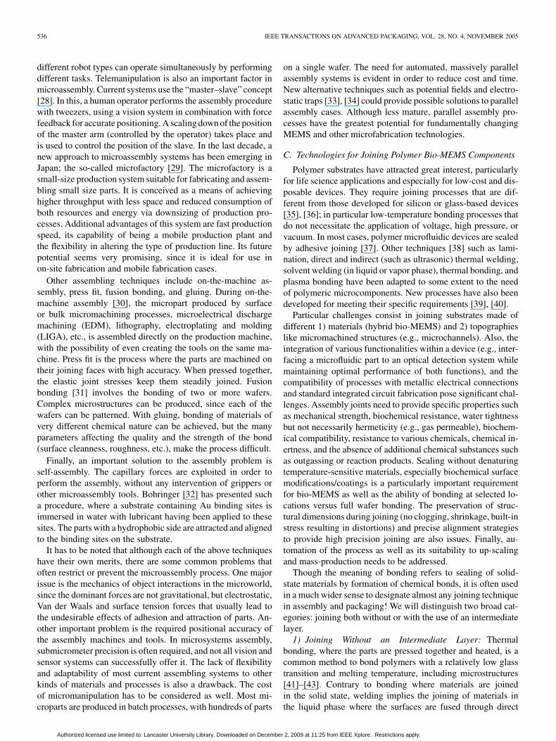
Fig. 1. Ultrathin interconnect (10 �m) for highly flexible foldable systems.
Fig. 2. Ultrasmall hearing aid using 0201 SMD components and two solderedflip chips (product courtesy Phonak AG, Switzerland).
A crucial development in order to maximize these goals hasbeen the development of ultrathin silicon devices as well asrerouting techniques to enable high-volume, low-cost manufac-turing. The capability to fabricate thin integrated circuits (Ics) toless than 50 m thickness, thereby minimizing the total heightof the assembly to a mere breadth of a human hair, is the en-abling technology for flat and flexible systems. Also, respectiveinterconnect techniques are required in order to maintain theseideal properties (Fig. 1).
The thin electronic chips show a high mechanical flexibilitycomparable to polymeric foils and are, therefore, ideally suitedfor assembly on polymer tapes. Functional tests have shownthat, especially for digital chips, a given radius of curvature ofthe silicon itself has no detrimental effect on the performance.A total system thickness of less than 60 m enables new and in-novative treatment and diagnosis methods, which were not pos-sible until now.
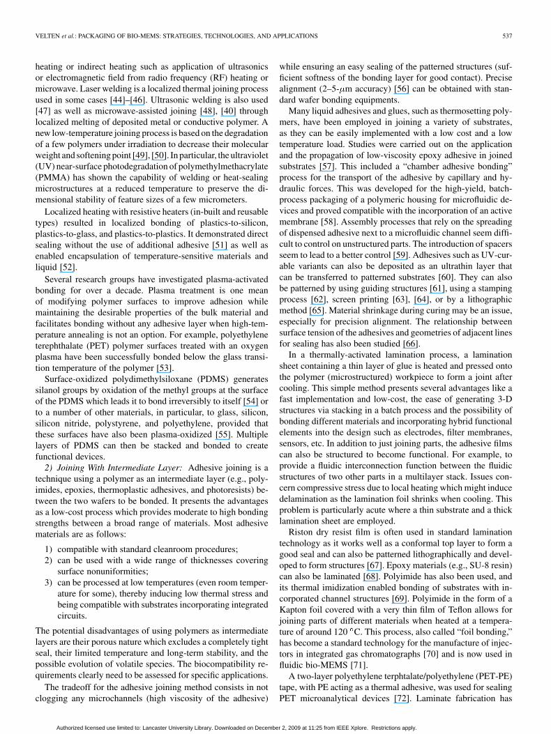
When ultrathin chips are not an option, the use of standardthickness chips can still enable extremely small devices by theuse of flip-chip technology. Hearing aids are an excellent ex-ample which demonstrates the evolution from large boxes wornaround the neck, to those now small enough to incorporate high-performance digital signal processor (DSP), microcontrollers,microphones, and batteries in one tiny in-the-ear device (Fig. 2).
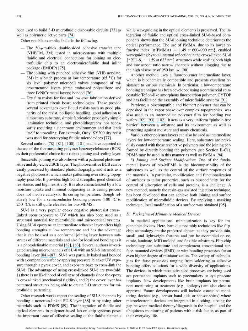
In order to increase the functionality per unit volume and si-multaneously keep a given process flow (such as surface-mounttechnology (SMT)) the mounting, of bare die chips in an SMD-compatible form factor is possible. Sometimes termed chip scalepackages (CSP), these can be mounted together with other SMDcomponents in a high-volume capable process [96] without theneed for special high-precision bonding equipment and/or ultra-fine-line substrate technology. Examples here are pacemaker ordefibrillator units, which employ digital and analog high-perfor-mance chips, which in a packaged or wire-bonded format wouldrequire significantly more space and weight (Fig. 3).
Fig. 3. Rerouted chip set for implementing higher functionality into apacemaker device (product courtesy Biotronik GmbH, Germany).
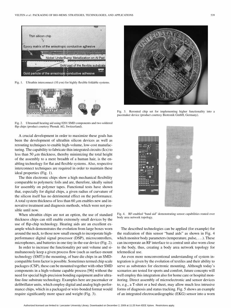
Fig. 4. RF-enabled “band aid” demonstrating sensor capabilities routed overbody area network topology.
The described technologies can be applied (for example) forthe realization of thin sensor “band aids” as shown in Fig. 4which monitor body parameters (temperature, pulse, ). Thesecan incorporate an RF interface to a central unit also worn closeto the body, thus, creating a body area network topology fortelemedical use.
An even more nonconventional understanding of system in-tegration is given by the evolution of textiles and their ability toserve as substrates for electronic mounting. Although today’sscenarios are tested for sports and comfort, future concepts willwell employ this integration also for home care or hospital mon-itoring. Direct assembly of microelectronic and sensor devicesto, e.g., a T-shirt or a bed sheet, may allow much less intrusiveforms of diagnosis and status tracking. Fig. 5 shows an exampleof an integrated electrocardiographic (EKG) sensor into a worn
Authorized licensed use limited to: Lancaster University Library. Downloaded on December 2, 2009 at 11:25 from IEEE Xplore. Restrictions apply.
540 IEEE TRANSACTIONS ON ADVANCED PACKAGING, VOL. 28, NO. 4, NOVEMBER 2005
Fig. 5. EKG T-Shirt with textile pads, conductive fibers woven into the fabric(courtesy of TITV Greiz, Germany).
T-shirt. The cables are currently required only to verify the per-formance against a metallic thread woven into the fabric of thetextile.
E. Packaging of Biosensors for In Vitro Applications
Microfluidics and biochip-compatible packaging are the typ-ical enabling technologies which can convert a bare biochipinto a device practically usable in the macroworld. Furthermore,packaging represents a major contribution to fabrication costs,which is a special challenge for the development of single-usedevices.
Microfluidic technology provides the interface for the fluidsupply of miniaturized biosensor elements. The basic objectiveis an efficient and reproducible mass transfer between solutionand the specific bioaffinity layer. Microfluidic solutions offershort diffusion lengths and a high surface-to-volume ratio whichallows rapid mass transfer yielding short reaction times, and re-quiring minute amounts of analytes and reagents [97], [98].
Here, we report the development of a microfluidic module fora multianalyte biochip based on an array of nine monolithic op-toelectronic transducers (BIOMIC chip) and its packaging in theprototype stage. The microfluidics and packaging technologiesas described in this article represent important steps in devel-oping a user-friendly, practically usable multianalyte biosensordevice from a bare biochip. This development aims at a proto-type device that can be applied for the evaluation of the biochip’sanalytical properties and the implementation of suitable assaysin the field of medical diagnostic testing.
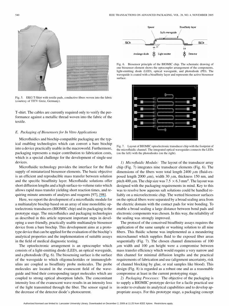
The optoelectronic arrangement is an optocoupler whichconsists of a light-emitting diode (LED), an optical waveguide,and a photodiode (Fig. 6). The biosensing surface is the surfaceof the waveguide to which oligonucleotides or immunoglob-ulins are coupled as bioaffinity probe molecules. The probemolecules are located in the evanescent field of the wave-guide and bind their corresponding target molecules which arecoupled to strong optical absorption labels. The concomitantintensity loss of the evanescent wave results in an intensity lossof the light transmitted through the fiber. The sensor signal isthe decrease of the detector diode’s photocurrent.
Fig. 6. Biosensor principle of the BIOMIC chip. The schematic drawing ofone biosensor element shows the optocoupler arrangement of the components,light-emitting diode (LED), optical waveguide, and photodiode (PD). Thewaveguide is coated with a bioaffinity layer and represents the active biosensorsurface.
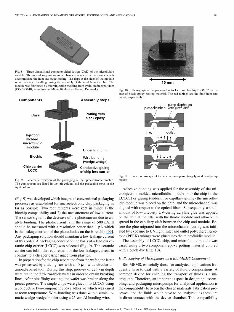
Fig. 7. Layout of BIOMIC optoelectronic transducer chip with the footprint ofthe microfluidic channel. The integrated optical waveguides connects the LEDs(on the left) with the photodiodes (on the right).
1) Microfluidic Module: The layout of the transducer arraychip (Fig. 7) integrates nine transducer elements (Fig. 6). Thedimensions of the fibers were total length 2400 m (fluid-ex-posed length 2000 m), width 30 m, thickness 150 nm, andpitch 400 m. The chip size was 7.5 6.3 mm . The layout wasdesigned with the packaging requirements in mind. Key to thiswas to resolve how aqueous salt solutions could be handled re-liably on a microelectronic chip. The wetted biosensor surfaceson the optical fibers were separated by a broad sealing area fromthe electric domain with the contact pads for wire bonding. Toenable a broad sealing a large distance between bond pads andelectronic components was chosen. In this way, the reliability ofthe sealing was strongly improved.
The protocol of the conceived bioaffinity assays requires theapplication of the same sample or washing solution to all ninefibers. This fluidic scheme was implemented as a meanderingmicrochannel which supplies fluid to the exposed fiber areassequentially (Fig. 7). The chosen channel dimensions of 100
m width and 100 m height were a compromise betweenmass transfer efficiency which would require a very narrow andthin channel for minimal diffusion lengths and the practicalrequirements of fabrication and use (alignment uncertainty, riskof channel blocking by glue, or real samples like blood). Thisdesign (Fig. 8) is regarded as a robust one and as a reasonablecompromise at least in the current prototyping stage.
2) Packaging Processes: The objective of the packaging isto supply a BIOMIC prototype device for a facile practical usein order to evaluate its analytical capabilities and to develop ap-propriate assays. For this prototype stage, a packaging concept
Authorized licensed use limited to: Lancaster University Library. Downloaded on December 2, 2009 at 11:25 from IEEE Xplore. Restrictions apply.
VELTEN et al.: PACKAGING OF BIO-MEMS: STRATEGIES, TECHNOLOGIES, AND APPLICATIONS 541
Fig. 8. Three-dimensional computer-aided design (CAD) of the microfluidicmodule. The meandering microfluidic channel connects the two holes whichaccommodate the inlet and outlet tubing. The flaps at the sides of the moduleserve the easier handling during the assembly of the module to the chip. Themodule was fabricated by microinjection molding from cyclo-olefin copolymer(COC) (SMB, Scandinavian Micro Biodevices, Farum, Denmark).
Fig. 9. Schematic overview of the packaging of the optoelectronic biochip.The components are listed in the left column and the packaging steps in theright column.
(Fig. 9) was developed which integrated conventional packagingprocesses as established for microelectronic chip packaging asfar as possible. Two requirements were kept in mind: 1) thebiochip-compatibility and 2) the measurement of low current.The sensor signal is the decrease of the photocurrent due to an-alyte binding. The photocurrent is in the range of 500 pA. Itshould be measured with a resolution better than 1 pA whichis the leakage current of the photodiodes on the bare chip [99].Any packaging solution should maintain a low leakage currentof this order. A packaging concept on the basis of a leadless ce-ramic chip carrier (LCCC) was selected (Fig. 9). The ceramiccarrier can fulfill the requirement of the low leakage current incontrast to a cheaper carrier made from plastics.
In preparation for the chip separation from the wafer, the latterwas processed by a dicing saw with a 40- m-wide circular di-amond-coated tool. During this step, grooves of 225 m depthwere cut in the 525- m-thick wafer in order to obtain breakinglines. After bioaffinity coating, the wafer was broken along theprecut grooves. The single chips were glued into LCCCs usinga conductive two-component epoxy adhesive which was curedat room temperature. Wire-bonding was done with a semiauto-matic wedge-wedge bonder using a 25- m Al bonding wire.
Fig. 10. Photograph of the packaged optoelectronic biochip BIOMIC with acase of black epoxy potting material. The red tubings are the fluid inlet andoutlet, respectively.
Fig. 11. Funcion principle of the silicon micropump (supply mode and pumpmode).
Adhesive bonding was applied for the assembly of the mi-croinjection-molded microfluidic module onto the chip in theLCCC. For gluing (underfill or capillary gluing) the microflu-idic module was placed on the chip, and the microchannel wasaligned with respect to the optical fibers. Subsequently, a smallamount of low-viscosity UV-curing acrylate glue was appliedon the chip at the fillet with the fluidic module and allowed tospread in the capillary cleft between the chip and module. Be-fore the glue migrated into the microchannel, curing was initi-ated by exposure to UV light. Inlet and outlet polyetheretherke-tone (PEEK) tubings were glued into the microfluidic module.
The assembly of LCCC, chip, and microfluidic module wascased using a two-component epoxy potting material coloredwith a black dye (Fig. 10).
F. Packaging of Micropumps as a Bio-MEMS Component
Bio-MEMS, especially those for analytical applications fre-quently have to deal with a variety of fluidic compositions. Acommon device for enabling the transport of fluids is a mi-cropump. Therefore, an important aspect in designing, assem-bling, and packaging micropumps for analytical application isthe compatibility between the chosen materials, fabrication pro-cesses, and the fluids which have to be analyzed, as these arein direct contact with the device chamber. This compatibility
Authorized licensed use limited to: Lancaster University Library. Downloaded on December 2, 2009 at 11:25 from IEEE Xplore. Restrictions apply.
542 IEEE TRANSACTIONS ON ADVANCED PACKAGING, VOL. 28, NO. 4, NOVEMBER 2005
Fig. 12. Full wafer strategy for the assembly of the micropumps.
also applies to the micropump package which often incorpo-rates inlet and outlet ports of the packaged micropump.
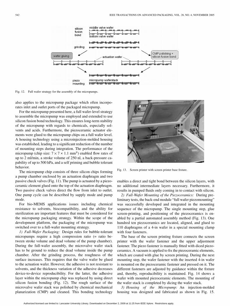
For the micropump presented here, a full wafer-level strategyto assemble the micropump was employed and extended to usesilicon fusion bond technology. This ensures long-term stabilityof the micropump with regards to chemicals, especially sol-vents and acids. Furthermore, the piezoceramic actuator ele-ments were glued to the micropump chips on a full wafer level.A housing technology using a microinjection-molded housingwas established, leading to a significant reduction of the numberof mounting steps during integration. The performance of themicropump (chip size: 7 7 1.1 mm ) enabled flow rates ofup to 2 ml/min, a stroke volume of 250 nl, a back-pressure ca-pability of up to 500 hPa, and a self priming and bubble tolerantbehavior.
The micropump chip consists of three silicon chips forminga pump chamber enclosed by an actuation diaphragm and twopassive check valves (Fig. 11). The pump is actuated by a piezo-ceramic element glued onto the top of the actuation diaphragm.Two passive check valves direct the flow from inlet to outlet.One pump cycle can be described by supply mode and pumpmode.
For bio-MEMS applications issues including chemicalresistance to solvents, biocompatibility, and the ability forsterilization are important features that must be considered forthe micropump packaging strategy. Within the scope of thedevelopment platform, the packaging of the micropump wasswitched over to a full-wafer mounting strategy.
1) Full-Wafer Packaging: Design rules for bubble-tolerantmicropumps require a high compression ratio (= ratio be-tween stroke volume and dead volume of the pump chamber).During the full-wafer assembly, the microvalve wafer stackhas to be ground to reduce the dead volume inside the pumpchamber. After the grinding process, the roughness of thesurface increases. This requires that the valve wafer be gluedto the actuation wafer. However, the adhesive is not resistant tosolvents, and the thickness variation of the adhesive decreasesdevice-to-device reproducibility. For the latter, the adhesivelayer within the micropump chip was replaced by using directsilicon fusion bonding (Fig. 12). The rough surface of themicrovalve wafer stack was polished by chemical mechanicalplanarization (CMP) and cleaned. This bonding technology
Fig. 13. Screen printer with screen printer base fixture.
enables a direct and tight bond between the silicon layers, withno additional intermediate layers necessary. Furthermore, itresults in pumped fluids only coming in to contact with silicon.
2) Full-Wafer Mounting of the Piezoceramics: During pre-liminary tests, the back-end module “full wafer piezomounting”was successfully developed and integrated in the mountingsequence of the micropump. The single mounting step, gluescreen-printing, and positioning of the piezoceramics is en-abled by a partial automated assembly method (Fig. 13). Onehundred ten piezoceramics are located, aligned, and glued to110 diaphragms of a 4-in wafer in a special mounting clampwith four fasteners.
The base of the screen printing fixture connects the screenprinter with the wafer fastener and the upper adjustmentfastener. The piezo fastener is manually fitted with diced piezo-ceramics. A vacuum is applied to fix the piezoceramic elements,which are coated with glue by screen printing. During the nextmounting step, the wafer fastener with the inserted 4-in waferis mounted on the piezoceramic fastener and pressed on it. Thedifferent fasteners are adjusted by guidance within the fixtureand, thereby, reproducibility is maintained. Fig. 14 shows awafer with mounted piezoceramic elements. The mounting ofthe wafer stack is completed by dicing the wafer stack.
3) Housing of the Micropump: An injection-moldedhousing was designed and fabricated as shown in Fig. 15.
Authorized licensed use limited to: Lancaster University Library. Downloaded on December 2, 2009 at 11:25 from IEEE Xplore. Restrictions apply.
VELTEN et al.: PACKAGING OF BIO-MEMS: STRATEGIES, TECHNOLOGIES, AND APPLICATIONS 543
Fig. 14. 4–in wafer with piezo ceramics.
Fig. 15. Realization of the injection molding housing.
The tool kit for this injection molding housing required thefollowing features:
— the mounting of the micropump chip (7 7 1.1 mm )realized on a plateau with adjustment marks;
— the adhesive for chip mounting deposited by screen-printing spacers ensuring an exact layer thickness;
— the design of the package to ensure a direct wire-bondfrom the silicon chip and piezoceramic elements to elec-trical interconnection pins;
— the integration of electrical interconnection pins by insertinjection molding, including strain relief for the electricalinterconnection.
— The employment of an injection-molded solvent-resistantplastic cover to protect the piezo against humidity anddegradation during sterilization.
III. CONCLUSION
Packaging of bio-MEMS plays an important role in pro-viding bio-MEMS with an interface to the macroworld of theuser. Many of the employed packaging methods stem from thepackaging of nonbio-MEMS and have been adapted to biolog-ical or medical requirements. A new trend of using polymerbio-MEMS, mainly because of perceived economic reasons,has become evident. Many of the techniques known frompackaging silicon-based MEMS cannot be applied to polymer
bio-MEMS. In this paper, conventional packaging technologies,as well as novel technologies especially developed for polymerMEMS, have been presented. Considerations on strategies forpartitioning subsystems within integrated subsystems havealso been presented. These strategies strongly influence thenumber of packaging steps necessary for assembling the wholesystem and, thus, influence the costs of manufacture in whichthe packaging costs account for a very significant component.Several approaches for microassembly of hybrid microscaledevices have been presented. These all aim to provide a meansfor the rapid, simple, and reliable positioning, orientating, andassembling of microcomponents into complex microsystems inorder to enable a high-yield and throughput by unit reductionof microassembly costs.
Special applications of bio-MEMS packaging such as pack-aging of a micropump for biological applications and packagingof a biosensor for analytical tasks have been presented. Withinthe packaged micropump, the fluid contacts only with three ma-terials: 1) silicon, 2) the plastics of the housing, and 3) one gluebetween the housing and chip, to be selected depending on therequirements of the application. With that, this micropump canbe used in various bio-MEMS applications.
The presented BIOMIC biosensor was packaged to enable anearly practical evaluation in the product development processwhich is an important asset in rapid product development. Therelatively low yield of commercial biosensor developments canbe attributed to a lack of feasible, functional, and economicpackaging technology which hampers the transformation of ascientific biosensor into a commercial device. The selectionof technologies for prototyping is also an important economicfactor since the transformation mentioned above requires themajor portion of the development costs.
It is important to note the interdependence of the various mi-crofabrication and assembly processes in the packaging chain.The chip layout design with the clearly separated functional do-mains, for instance, was a good basis for the chosen packagingtechniques. It is clear that biochip design, fabrication, and pack-aging should be implemented as an integrated process.
The examples presented for the packaging of bio-MEMSdemonstrate that the choice of materials and processes forpackaging are much more stringent for bio-MEMS than forpure technical MEMS. The same applies in some cases to therequired density of packaging. An example are tiny medical im-plants. Here, the costs are less important than the size with theconsequence that the most sophisticated packaging techniquescan be applied.
ACKNOWLEDGMENT
T. Velten and H. Ruf would like to thank the other partnersin the BIOMIC consortium for their fruitful and enjoyablecollaboration. H. Ruf would also like to thank L. B. Larsen,from Nunc, Roskilde, Denmark, as well as M. Denningerand R. Haupt, from SMB, Lyngby, Denmark, for fabricatingthe microfluidic module and performing the underfill gluingof this module. He would also like to thank K. Misiakosfrom the Institute of Microelectronics/National Center forScientific Research “DEMOKRITOS,” Greece, who devel-oped the BIOMIC biosensor chip and who provided drawings
Authorized licensed use limited to: Lancaster University Library. Downloaded on December 2, 2009 at 11:25 from IEEE Xplore. Restrictions apply.
544 IEEE TRANSACTIONS ON ADVANCED PACKAGING, VOL. 28, NO. 4, NOVEMBER 2005
of this chip. C. K. Malek would like to thank both Dr. R.Truckenmüller from the Institut für Mikrostrukturtechnik,Forschungszentrum Karlsruhe GmbH, for providing valuablematerials and comments and Prof. O. Geschke, Mikroelek-tronik Centret (MIC), Technical University of Denmark, forhelpful comments on bonding polymers. The authors wouldalso like to thank S. Taylor of Cardiff University for the helpfulmanuscript revisions. Also, the writing of this review articlewas carried out within the framework of the EC Network ofExcellence “Multi-Material Micro Manufacture: Technologiesand Applications (4M).”
REFERENCES
[1] R. Bashir, “BioMEMS: State-of-the-art in detection, opportunities andprospects,” Adv. Drug Delivery Rev., vol. 56, pp. 1565–1586, 2004.
[2] A. Manz et al., “Miniaturized total chemical analysis systems. A novelconcept for chemical sensing,” Sens. Actuators B, Chem., vol. B1, pp.249–255, 1990.
[3] H. Becker et al., “Polymer microfluidic devices,” Talanta, vol. 56, pp.267–287, 2002.
[4] S. Guillaudeu et al., “Fabrication of 2-�m-wide poly-crystalline dia-mond channels using silicon molds for micro-fluidic applications,” Di-amond Rel. Mater. , vol. 12, pp. 65–69, 2003.
[5] G. Kotzar et al., “Evaluation of MEMS materials of construction forimplantable medical devices,” Biomater., vol. 23, pp. 2737–2750, 2002.
[6] R. S. Shawgo et al., “BioMEMS for drug delivery,” Current OpinionSolid-State Mater. Sci., vol. 6, pp. 329–334, 2004.
[7] K. Lee and L. Lin, “Surface micromachined glass and polysilicon mi-crochannels using MUMP’s for BioMEMS applications,” Sens. Actua-tors A, Phys., vol. 111, pp. 44–50, 2004.
[8] B. Ziaie et al., “Hard and soft micromachining for BioMEMS: Reviewof techniques and examples of applications in microfluidics and drugdelivery,” Adv. Drug Delivery Rev., vol. 56, pp. 145–172, 2004.
[9] S. Bouaidat et al., “Plasma-polymerized coatings for bio-MEMS appli-cations,” Sens. Actuators A: Phys., pp. 390–394, 2004.
[10] H. Becker and L. Locascio, “Polymer microfluidic devices,” Talanta,vol. 56, pp. 267–287, 2002.
[11] J. J. Cefai and D. A. Barrow, “Integrated chemical analysis microsystemsfor life sciences research in space,” J. Micromech. Microeng., vol. 4, pp.172–185, 1994. [Invited review in Special Microfluidics edition].
[12] S. Fiehm, S. Howitz, M. T. Pham, T. Vopel, M. Burger, and T. We-gener, “Components and technology for a fluidic-ISFET-Microsystem.,”in Proc. �TAS Workshop, A. van den Berg and P. Bergveld, Eds. Twente,Dordrecht, The Netherlands, Nov., 21–22 1994, pp. 289–293. (1995).
[13] J. H. Fluitman et al., “Micromechanical components for�TAS,” in Proc.�TAS Workshop, A. van den Berg and P. Bergveld, Eds. Twente, Dor-drecht, The Netherlands, Nov., 21–22 1994, pp. 73–83. 1994.
[14] S. Drost et al., “Microanalytical systems for environmental control:Aims, structure and integration of �TAS-modules,” in Proc. �TASWorkshop, H. M. Widmer, E. Verpoorte, and S. Barnard, Eds. Basel,Switzerland, Nov. 19–22, 1996, pp. 199–202. 1996.
[15] M. Koch et al., “Micromachined chemical reaction system,” Sens. Actu-ators A, Phys., vol. 74, pp. 207–210.
[16] J. T. Butler et al., “Advanced multichip packaging of micro-electro-mechanical systems,” in Int. Proc. Conf. Solid-State Sens. Actuators,Jun. 1997, pp. 261–264.
[17] A. Morrissey et al., “3D packaging of a microfluidic system with sensoryapplications,” Micromach. Devices Compon. III, vol. 3224, pp. 161–168,1997.
[18] S. Chen et al., “Laser-based microscale patterning of biodegradablepolymers for biomedical applications,” Int. J. Mater. Product Technol.,vol. 18, pp. 457–468, 2003.
[19] T. Bauer et al., “Development of an industrial femtosecond micro-ma-chining system,” Proc. SPIE, vol. 4633, pp. 128–135, 2002.
[20] P. W. Cooley et al., “Application of ink-jet printing technology toBioMEMS and microfluidic systems,” in Proc. SPIE MicrofluidicsBioMEMS Conf., San Francisco, CA, Oct. 22–25, 2001, pp. 177–188.
[21] I. Uematsu et al., “Surface morphology and biological activity of proteinthin films produced by electrospray deposition,” J. Coll. Interface Sci.,vol. 269, pp. 336–340, 2004.
[22] S. Zimmermann et al., “In-device enzyme immobilization: Wafer-levelfabrication of an integrated glucose,” Sens. Actuators B, Chem., vol. 99,pp. 163–173, 2004.
[23] H. C. Huang et al., “Photo-lithographically impregnated and molecu-larly imprinted polymer thin film for biosensor applications,” J. Chro-matography A, vol. 1027, pp. 263–268, 2004.
[24] A. Tseng, W. Tang, Y. Lee, and J. Allen, “NSF 2000 workshop on man-ufacturing of micro-electro-mechanical systems,” J. Mater. Process.Manuf. Sci., vol. 8, pp. 295–300, Apr. 2000.
[25] H. Van Brussel, J. Peirs, A. Delchambre, G. Reinhart, N. Roth, M. Weck,and E. Zussman, “Keynote papers presented at the opening session, as-sembly of microsystems,” Ann. CIRP, vol. 49/2/2000, pp. 452–456.
[26] Y. Zhou, B. Nelson, and B. Vikramaditya, “Fusing force and vision feed-back for micromanipulation,” in Proc. ICRA, Int. Conf. Robotics Autom.,1998, pp. 1220–1225.
[27] A. Mardanov, J. Seyfried, and S. Fatikow, “An automated assemblysystem for a microassembly station,” in Computers in Industry. NewYork: Elsevier, 1999, vol. 38, pp. 93–102.
[28] K. Kaneko, H. Tokashiki, K. Tanie, and K. Komoriya, “Impedanceshaping based on force feedback bilateral control in macro-microteleoperation system,” in Proc. ICRA, 1997, pp. 710–717.
[29] M. Tanaka, “Development of desktop machining microfactory,” RIKENreview no. 34, pp. 46–49, Apr. 2001. Focused on Advances on Micro-Mechanical Fabrication Techniques.
[30] H. Langen, T. Masuzawa, and M. Fujino, “Modular method for mi-croparts machining and assembly with self-alignment,” Ann. CIRP, vol.44/1, pp. 173–176.
[31] M. Schmidt, “Silicon wafer bonding for micromechanical devices,”in Solid-State Sensor and Actuator Workshop, Hilton Head, SC, Jun.13–16, 1994, pp. 127–131.
[32] K. Bohringer, “Surface modification and modulation in microstructures:Controlling protein adsorption, monolayer desorption and micro-self-assembly,” J. Micromech. Microeng., pp. 1–10, 2003.
[33] K. Bohringer, M. Cohn, K. Goldberg, R. Howe, and A. Pisano, “Parallelmicroassembly with electrostatic force fields,” in Proc. IEEE Int. Conf.Robotics and Automation (ICRA), vol. 2, Leuven, Belgium, May 1998,pp. 1204–1211.
[34] J. Luo and L. Kavraki, “Part assembly using static and dynamic forcefields,” in Proc. IEEE/RSJ Int. Conf. Intelligent Robots and Systems(IROS). Piscataway, Nov. 2000, pp. 1468–1474.
[35] E. Verpoorte and N. F. de Rooij, “Microfluidic meets MEMS,” in Proc.IEEE, vol. 91, Jun. 2003, pp. 930–953.
[36] G. Perozziello, “Packaging of microsystems,” in Microsystem Engi-neering of Lab-on-a Chip Devices. New York: Wiley, 2003, ch. 9. , O.Geschke, H. Klank, and P. Telleman.
[37] M. Tavakoli, “Adhesive bonding of medical and implantable devices,”Business Briefing Medical Device and Manuf. Technol., pp. 1–12, 2002.
[38] Handbook of Plastics, Elastomers, and Composites, 3rd ed., McGraw-Hill, New York, 1996. C. A. Harper, Joining of plastics, elastomers, andcomposites.
[39] H. Becker and C. Gärtner, “Polymer microfabrication methods for mi-crofluidic analytical applications,” Electrophoresis, vol. 21, no. 1, pp.12–26, 1999.
[40] M. Schuenemann, D. Thomson, M. Atkins, S. Garst, A. Yussuf, M.Solomon, J. Hayes, and E. Harvey, “Packaging of disposable chips forbionanalytical applications,” in IEEE Proc. Electronic ComponentsTechnology Conf., 2004, pp. 853–861.
[41] G. A. C. M. Spierings, J. Haisma, and F. J. H. M. van der Kruis, “Directbonding of organic polymeric materials,” Philips J. Res., vol. 49, pp.139–149, 1995.
[42] F. Bundgard, T. Nielsen, D. Nillson, P. Shi, G. Perozziello, A. Kris-tensen, and O. Geschke, “Cyclic olefin copolymer (COC/TOPAS—Anexceptional material for exceptional lab-on-chip systems,” in Proc. 8thInt. Conf. Miniaturised Systems Chemistry Life Sciences�TAS, T. Lau-rell, J. Nilsson, K. Jensen, D. J. Harrison, and J. P. Kutter, Eds., Malmö,Sweden, Sep. 26–30, 2004, pp. 372–374.
[43] A. Han, M. Graf, O. Wang, S. K. Mohanty, K.-H. Han, and A. B. Frazier,“A multilayer plastic/glass technology for microfluidic systems with in-tegrated functionality,” in Proc. IEEE 12th Int. Conf. Transducers, 2003,pp. 1315–1318.
[44] H. Klank, J. P. Kutter, and O. Geschke, “CO -laser micromachining andback-end processing for rapid production of PMMA-based microfluidicsystems,” Lab on a Chip, vol. 2, pp. 242–246, 2002.
[45] R. Witte, H. J. Herfurth, and I. Bauer, “Microjoining of dissimilar ma-terials for optoelectronic and biomedical applications,” Proc. SPIE, vol.4979, pp. 226–232, 2003.
[46] J. Lai, X. Chen, X. Wang, X. Yi, and S. Liu, “Laser bonding and pack-aging of plastic microfluidic chips,” in Proc. IEEE ICEPT, 2003, pp.168–171.
[47] J. Bahrs, “Ultraschallschweissen von polymeren mikrostrukturen,”Diploma thesis, Karlsruhe, Germany, 2004. Research Center Karlsruhe,Professional Sch. Technol. Esslingen.
Authorized licensed use limited to: Lancaster University Library. Downloaded on December 2, 2009 at 11:25 from IEEE Xplore. Restrictions apply.
VELTEN et al.: PACKAGING OF BIO-MEMS: STRATEGIES, TECHNOLOGIES, AND APPLICATIONS 545
[48] K. F. Lei, W. J. Li, N. Budraa, and J. D. Mai, “Microwave bonding ofpolymer-based substrates for micro/nano fluidic applications,” in Proc.IEEE 12th Int. Conf. Transducers, 2003, pp. 1335–1338.
[49] H. S. Lee, D. S. Kim, and T. H. Kwon, “A novel low temperature bondingtechnique for plastic substrates using X-ray irradiation,” in Proc. IEEE12th Int. Conf. Transducers, 2003, pp. 1331–1334.
[50] R. Truckenmüller, P. Henzi, D. Herrmann, V. Saile, and W. K. Schom-burg, “Bonding of polymer microstructures by UV irradiation and sub-sequent welding at low temperatures,” J. Microsyst. Technol., vol. 10,pp. 372–374, 2004.
[51] K. Wulff, Z. Rummler, and W. K. Schomburg, “Hybride drucksensorenaus kunstoff und glas nach dem AMANDA-verfahren,” Ph.D. disserta-tion, University of Karlsruhe, Karlsruhe, Germany, 2001.
[52] Y.-C. Su and L. Lin, “Localized plastic bonding for micro assembly,packaging and liquid encapsulation,” in Proc. IEEE MEMS Conf., 2001,pp. 50–53.
[53] Z. Wu, N. Xanthopoulos, F. Reymond, J. S. Rossier, and H. H.Girault, “Polymer microchips bonded by O -plasma activation,” Elec-trophoresis, vol. 23, pp. 782–790, 2002.
[54] D. C. Duffy, J. C. McDonald, O. J. A. Schueller, and G. M. Whitesides,“Rapid prototyping of microfluidic systems in poly(dimethylsiloxane),”Anal. Chem., vol. 70, pp. 4974–4984, 1998.
[55] J. C. Mc Donald and G. M. Whitesides, “Poly(dimethylsiloxane) as amaterial for fabricating microfluidic devices,” Accounts Chem. Res., vol.35, no. 7, pp. 491–499, 2001.
[56] F. Niklaus, P. Enoksson, E. Kälvesten, and G. Stemme, “A method tomaintain wafer alignment precision during adhesive wafer bonding,”Sens. Actuators A, vol. 107, pp. 273–278, 2003.
[57] A. Gerlach, H. Lambach, and D. Seidel, “Propagation of adhesivesin joints during capillary adhesive bonding of microcomponents,”Microsyst. Technol., vol. 6, pp. 19–22, 1999.
[58] C. Fu, T. Koller, R. Ahrens, Z. Rummler, and W. K. Schomburg, “Op-timization of chamber adhesive bonding for packaging of microcompo-nents,” in Proc. Eurosensors XVI, 2002, pp. 149–150.
[59] P. Friis, E. K. Storm, K. Hoppe, and J. Janting, “Adhesive bondingmethods for polymer microTAS components,” in Proc. �TAS, 2004, pp.354–356.
[60] J. Kentsch, W. Lutz, M. Dürr, and M. Stelzle, “High precision tempera-ture bonding process for bioMEMS,” Proc. �TAS, pp. 19–21, 2004.
[61] Z. Huang, J. C. Sanders, C. Dunsmor, H. Ahmadzadeh, and J. P. Landers,“A method for UV-bonding in the fabrication of glass electrophoreticmicrochips,” Electrophoresis, vol. 22, pp. 3924–3929, 2001.
[62] S. Schlautmann, G. A. J. Besselink, R. Prabhu, and R. M. B. Schasfoort,“Fabrication of a microfluidic chip by UV bonding at room tempera-ture for integration of temperature-sensitive layers,” J. Micromech. Mi-croeng., vol. 13, pp. 81–84, 2003.
[63] J. Han, S. H. Lee, A. Puntambekar, S. Murugesan, J.-W. Choi, G.Beaucage, and C. H. Ahn, “UV adhesive bonding techniques at roomtemperature for plastic lab-on-a-chip,” in Proc. 7th Int. Conf. MicroTotal Analysis Systems (�TAS), Squaw Valley, CA, Oct. 5–9, 2003, pp.1113–1116. 2003.
[64] I. Chartier, C. Bory, A. Fuchs, D. Freida, N. Manaresi, M. Ruty, J. Bablet,K. Gilbert, N. Sarrut, F. Baleras, Ch. Villiers, and L. Fulbert, “Fabrica-tion of hybrid plastic-silicon micro-fluidics devices for individual cellmanipulation by dielectrophoresis,” Proc. SPIE, vol. 5345, pp. 7–16. Mi-crofluidics, BioMEMS, and Medical Microsystems II.
[65] C. Harrison, J. T. Cabral, C. M. Stafford, A. Karim, and E. J. Amis,“A rapid prototyping technique for the fabrication of solvent-resistantstructures,” J. Micromech. Microeng., vol. 14, pp. 153–156, 2004.
[66] J. Janting, E. K. Storm, and O. Geschke, “Surface tension drivenof adhesive microfluidic channel walls,” in Proc. �TAS, 2004, pp.378–380.
[67] M. O. Heuschkel, L. Guerin, B. Buisson, D. Bertrand, and P. Renaud,“Buried microchannels in photopolymer for delivering of solutions toneurons in a network,” Sens. Actuators B48 (1–3), pp. 356–361, 1998.
[68] L. J. Guérin, M. Bossel, M. Demierre, S. Calmes, and Ph. Renaud,“Simple and low cost fabrication of embedded micro-channels by usinga new thick-film photoplastic,” in Proc. IEEE Transducers, 1997, pp.1419–1421.
[69] S. Metz, R. Holzer, and P. Renaud, “Polyimide-based microfluidic de-vices,” Lab on a Chip, vol. 1, no. 1, pp. 29–34, 2001.
[70] J. A. Dziuban, “Portable gas chromatograph with integrated compo-nents,” J. Sens. Actuators A, vol. 115, pp. 318–330, 2004.
[71] S. Bargiel et al., Micromachined silicon-glass dosing device with built-inconductivity detector, in Eurosensors, Barcelona, Catalonia, Spain, Sep.2005. to be published.
[72] M. A. Roberts, J. S. Rossier, P. Bercier, and H. Girault, “UV laser ma-chined polymer substrates for the development of microdiagnostic sys-tems,” Anal. Chem., vol. 69, pp. 2035–2042, 1997.
[73] B. H. Weigl, R. L. Bardell, and C. R. Cabrera, “Lab-on-a-chip develop-ment,” Adv. Drug Delivery Rev., vol. 55, no. 3, pp. 349–377, 2003.
[74] T. Q. Truong and N.-T. Nguyen, “A polymeric piezoelectric micropumpbased on lamination technology,” J. Micromech. Microeng., vol. 14, pp.632–638, 2004.
[75] P. Galambos, G. L. Benavides, M. Okandan, M. W. Jenkins, and D. Het-herington, “Precision alignment packaging for microsystems with mul-tiple fluid connections,” in Proc. 2001 ASME Conf., New York, Nov.11–16, 2001, pp. 1–8.
[76] C. Fu, Z. Rummler, and W. Schomburg, “Magnetically driven micro ballvalves fabricated by multilayer adhesive film bonding,” J. Micromech.Microeng., vol. 13, pp. 96–102, 2003.
[77] P. Vulto, N. Glade, L. Altomarre, J. Bablet, L. Del Tin, G. Medoro,I. Chartier, N. Manaresi, M. Tartagni, and R. Guerrieri, “Microfluidicchannel fabrication in dry film resist for production and prototyping ofhybrid chips,” Lab on a Chip, vol. 5, no. 2, pp. 158–162, 2005.
[78] F. Niklaus, P. Enoksson, E. Kälvesten, and G. Stemme, “Low-tempera-ture full wafer adhesive bonding,” J. Micromech. Microeng., vol. 11, pp.100–107, 2001.
[79] T. K. Chou and K. Najafi, “3D MEMS fabrication using low-temperaturewafer bonding with benzocyclobutene (BCB),” in Proc. IEEE Trans-ducers Conf., 2001, pp. 1050–1573.
[80] P. Turmezei, A. Polyakov, J. R. Mollinger, M. Bartek, A. Bossche, and J.N. Burghartz, “Low-cost microfilter for red blood cell membrane stiff-ness measurement using photosensitive BCB,” in Proc. IEEE Trans-ducers, vol. 03, 2003, pp. 107–110.
[81] A. Jourdain, H. Ziad, P. De Moorr, and H. A. C. Tilmans, “Wafer-scale0-level packaging of (RF) MEMS devices using BCB,” in Proc. DTIP,2003, pp. 239–244.
[82] C.-T. Pan, Y. Yang, S.-C. Shen, M.-C. Chou, and H.-P. Chou, “A low-temperature wafer bonding technique using patternable materials,” Mi-cromech. Microeng., vol. 12, pp. 611–615, 2002.
[83] P. Svasek, E. Svasek, B. Lendl, and M. Vellekoop, “Fabrication of minia-turized fluidic devices using SU-8 based lithography and low tempera-ture wafer bonding,” J. Sens. Actuators A, vol. 115, pp. 591–599, 2004.
[84] R. J. Jackman, T. M. Floyd, R. Ghodssi, M. Schmidt, and K. F. Jensen,“Microfluidic systems with on-line UV detection fabricated in photode-finable epoxy,” J. Micromech. Microeng., vol. 11, pp. 263–269, 2001.
[85] S. Li, C. B. Freidhoff, and R. M. Young, “Fabrication of micronozzlesusing low-temperature wafer-level bonding with SU-8,” J. Micromech.Microeng., vol. 13, pp. 732–738, 2003.
[86] B. Helbo, A. Kristensen, and A. Menon, “A micro-cavity fluidic dyelaser,” J. Micromech. Microeng., vol. 13, pp. 307–311, 2004.
[87] J. Carlier, S. Ascott, V. Thomy, J. C. Fourrier, F. Caron, J. C. Camart,C. Druon, and P. Tabourier, “Integrated microfluidics based on multi-layered SU-8 for mass spectroscopy analysis,” J. Micromech. Microeng.,vol. 14, pp. 619–624, 2004.
[88] Y.-J. Chuang, F.-G. Tseng, J.-H. Cheng, and W.-K. Lin, “A novel fabri-cation method of embedded micro-channels by using SU-8 thick filmsphotoresists,” Sens. Actuators A, vol. 103, pp. 64–69, 2003.
[89] M. Ruano, V. Benoit, J. S. Aitchinson, and J. M. Cooper, “Flame hy-drolysis deposition of glass on silicon for the integration of optical andmicrofluidic devices,” Anal. Chem., vol. 72, pp. 1093–1097, 2000.
[90] B. Bilenberg, T. Nielsen, B. Clausen, and A. Kristensen, “PMMA toSU-8 bonding for polymer based lab-on-a-chip systems with integratedoptics,” J. Micromech. Microeng., vol. 14, pp. 814–818, 2004.
[91] K. W. Oh, A. Han, S. Bhansali, and C. H. Ahn, “A low-temperaturebonding technique using spin-on fluorocarbon polymers to assemble mi-crosystems,” Micromech. Microeng., vol. 12, pp. 187–191, 2001.
[92] H. S. Kim and K. Najafi, “Wafer bonding using parylene and wafer-leveltransfer of free-standing parylene membranes,” in Proc. IEEE Trans-ducers Conf., 2003, pp. 790–793.
[93] H.-S. Noh, Y. Choi, C. Wu, P. J. Hesketh, and M. G. Allen, “Rapid,low-cost fabrication of parylene microchannels for microfluidic applica-tions,” in IEEE Proc. Transducers 12th Int. Conf. Solid-State Sens., Ac-tuators, Microsyst., Boston, MA, Jun. 8–12, 2003, pp. 798–801. (2003).
[94] W. P. Eaton, S. H. Risbud, and R. L Smith, “Silicon-to-silicon bondingat T < 200 2C with polymethylmethacrylate,” Appl. Phys. Lett., vol.65, pp. 439–431, 1994.
[95] S. Lai, Y. Hudiono, and L. J. Lee, “Resin-gas injection technique forbonding and surface modification of polymer-based medical microde-vices,” Business Briefing Med. Device Manuf. Technol., pp. 1–4, 2002.
[96] M. Töpper et al., “Chip sized package—The option of choice for minia-turized medical devices,” in Proc. IMAPS , San Diego, CA, 1998.
[97] A. Manz and H. Becker, Eds., Microsystem Technology in Chemistry andLife Sciences. New York: Springer-Verlag, 1998.
[98] L. J. Kricka, “Microchips, microarrays, biochips, and nanochips: Per-sonal laboratories for the 21st century,” Clin. Chim. Acta., vol. 307, pp.219–223, 2001.
Authorized licensed use limited to: Lancaster University Library. Downloaded on December 2, 2009 at 11:25 from IEEE Xplore. Restrictions apply.
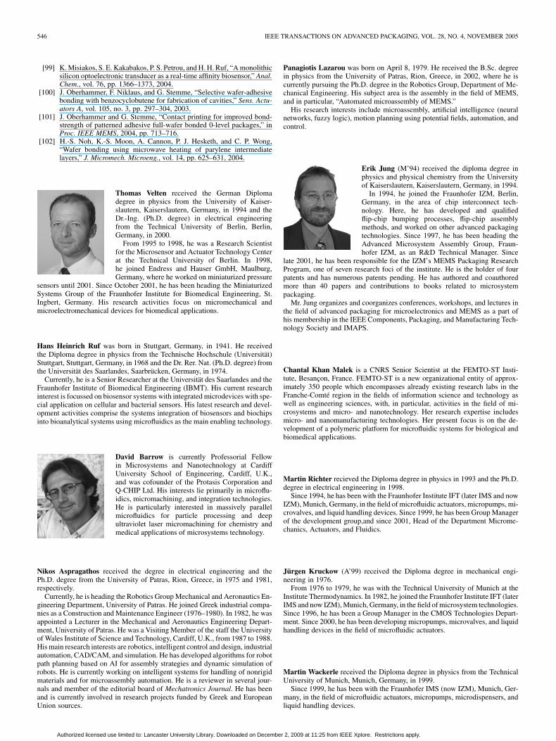
546 IEEE TRANSACTIONS ON ADVANCED PACKAGING, VOL. 28, NO. 4, NOVEMBER 2005
[99] K. Misiakos, S. E. Kakabakos, P. S. Petrou, and H. H. Ruf, “A monolithicsilicon optoelectronic transducer as a real-time affinity biosensor,” Anal.Chem., vol. 76, pp. 1366–1373, 2004.
[100] J. Oberhammer, F. Niklaus, and G. Stemme, “Selective wafer-adhesivebonding with benzocyclobutene for fabrication of cavities,” Sens. Actu-ators A, vol. 105, no. 3, pp. 297–304, 2003.
[101] J. Oberhammer and G. Stemme, “Contact printing for improved bond-strength of patterned adhesive full-wafer bonded 0-level packages,” inProc. IEEE MEMS, 2004, pp. 713–716.
[102] H.-S. Noh, K.-S. Moon, A. Cannon, P. J. Hesketh, and C. P. Wong,“Wafer bonding using microwave heating of parylene intermediatelayers,” J. Micromech. Microeng., vol. 14, pp. 625–631, 2004.
Thomas Velten received the German Diplomadegree in physics from the University of Kaiser-slautern, Kaiserslautern, Germany, in 1994 and theDr.-Ing. (Ph.D. degree) in electrical engineeringfrom the Technical University of Berlin, Berlin,Germany, in 2000.
From 1995 to 1998, he was a Research Scientistfor the Microsensor and Actuator Technology Centerat the Technical University of Berlin. In 1998,he joined Endress and Hauser GmbH, Maulburg,Germany, where he worked on miniaturized pressure
sensors until 2001. Since October 2001, he has been heading the MiniaturizedSystems Group of the Fraunhofer Institute for Biomedical Engineering, St.Ingbert, Germany. His research activities focus on micromechanical andmicroelectromechanical devices for biomedical applications.
Hans Heinrich Ruf was born in Stuttgart, Germany, in 1941. He receivedthe Diploma degree in physics from the Technische Hochschule (Universität)Stuttgart, Stuttgart, Germany, in 1968 and the Dr. Rer. Nat. (Ph.D. degree) fromthe Universität des Saarlandes, Saarbrücken, Germany, in 1974.
Currently, he is a Senior Researcher at the Universität des Saarlandes and theFraunhofer Institute of Biomedical Engineering (IBMT). His current researchinterest is focussed on biosensor systems with integrated microdevices with spe-cial application on cellular and bacterial sensors. His latest research and devel-opment activities comprise the systems integration of biosensors and biochipsinto bioanalytical systems using microfluidics as the main enabling technology.
David Barrow is currently Professorial Fellowin Microsystems and Nanotechnology at CardiffUniversity School of Engineering, Cardiff, U.K.,and was cofounder of the Protasis Corporation andQ-CHIP Ltd. His interests lie primarily in microflu-idics, micromachining, and integration technologies.He is particularly interested in massively parallelmicrofluidics for particle processing and deepultraviolet laser micromachining for chemistry andmedical applications of microsystems technology.
Nikos Aspragathos received the degree in electrical engineering and thePh.D. degree from the University of Patras, Rion, Greece, in 1975 and 1981,respectively.
Currently, he is heading the Robotics Group Mechanical and Aeronautics En-gineering Department, University of Patras. He joined Greek industrial compa-nies as a Construction and Maintenance Engineer (1976–1980). In 1982, he wasappointed a Lecturer in the Mechanical and Aeronautics Engineering Depart-ment, University of Patras. He was a Visiting Member of the staff the Universityof Wales Institute of Science and Technology, Cardiff, U.K., from 1987 to 1988.His main research interests are robotics, intelligent control and design, industrialautomation, CAD/CAM, and simulation. He has developed algorithms for robotpath planning based on AI for assembly strategies and dynamic simulation ofrobots. He is currently working on intelligent systems for handling of nonrigidmaterials and for microassembly automation. He is a reviewer in several jour-nals and member of the editorial board of Mechatronics Journal. He has beenand is currently involved in research projects funded by Greek and EuropeanUnion sources.
Panagiotis Lazarou was born on April 8, 1979. He received the B.Sc. degreein physics from the University of Patras, Rion, Greece, in 2002, where he iscurrently pursuing the Ph.D. degree in the Robotics Group, Department of Me-chanical Engineering. His subject area is the assembly in the field of MEMS,and in particular, “Automated microassembly of MEMS.”
His research interests include microassembly, artificial intelligence (neuralnetworks, fuzzy logic), motion planning using potential fields, automation, andcontrol.
Erik Jung (M’94) received the diploma degree inphysics and physical chemistry from the Universityof Kaiserslautern, Kaiserslautern, Germany, in 1994.
In 1994, he joined the Fraunhofer IZM, Berlin,Germany, in the area of chip interconnect tech-nology. Here, he has developed and qualifiedflip-chip bumping processes, flip-chip assemblymethods, and worked on other advanced packagingtechnologies. Since 1997, he has been heading theAdvanced Microsystem Assembly Group, Fraun-hofer IZM, as an R&D Technical Manager. Since
late 2001, he has been responsible for the IZM’s MEMS Packaging ResearchProgram, one of seven research foci of the institute. He is the holder of fourpatents and has numerous patents pending. He has authored and coauthoredmore than 40 papers and contributions to books related to microsystempackaging.
Mr. Jung organizes and coorganizes conferences, workshops, and lectures inthe field of advanced packaging for microelectronics and MEMS as a part ofhis membership in the IEEE Components, Packaging, and Manufacturing Tech-nology Society and IMAPS.
Chantal Khan Malek is a CNRS Senior Scientist at the FEMTO-ST Insti-tute, Besançon, France. FEMTO-ST is a new organizational entity of approx-imately 350 people which encompasses already existing research labs in theFranche-Comté region in the fields of information science and technology aswell as engineering sciences, with, in particular, activities in the field of mi-crosystems and micro- and nanotechnology. Her research expertise includesmicro- and nanomanufacturing technologies. Her present focus is on the de-velopment of a polymeric platform for microfluidic systems for biological andbiomedical applications.
Martin Richter recieved the Diploma degree in physics in 1993 and the Ph.D.degree in electrical engineering in 1998.
Since 1994, he has been with the Fraunhofer Institute IFT (later IMS and nowIZM), Munich, Germany, in the field of microfluidic actuators, micropumps, mi-crovalves, and liquid handling devices. Since 1999, he has been Group Managerof the development group,and since 2001, Head of the Department Microme-chanics, Actuators, and Fluidics.
Jürgen Kruckow (A’99) received the Diploma degree in mechanical engi-neering in 1976.
From 1976 to 1979, he was with the Technical University of Munich at theInstitute Thermodynamics. In 1982, he joined the Fraunhofer Institute IFT (laterIMS and now IZM), Munich, Germany, in the field of microsystem technologies.Since 1996, he has been a Group Manager in the CMOS Technologies Depart-ment. Since 2000, he has been developing micropumps, microvalves, and liquidhandling devices in the field of microfluidic actuators.
Martin Wackerle received the Diploma degree in physics from the TechnicalUniversity of Munich, Munich, Germany, in 1999.
Since 1999, he has been with the Fraunhofer IMS (now IZM), Munich, Ger-many, in the field of microfluidic actuators, micropumps, microdispensers, andliquid handling devices.
Authorized licensed use limited to: Lancaster University Library. Downloaded on December 2, 2009 at 11:25 from IEEE Xplore. Restrictions apply.