Optimized Micro-Via Technology for High Density and High Frequency (>40GHz) HermeticThrough-Wafer...
7
0-7803-8906-9/05/$20.00 ©2005 IEEE 2005 Electronic Components and Technology Conference Optimized Micro-Via Technology for High Density and High Frequency (>40GHz) Hermetic Through-Wafer Connections in Silicon Substrates R. Hauffe, A. Kilian, M. Winter, L. Shiv, G. Elger, M. Heschel, J. Kuhmann, S. Isaacs, S. Weichel, P. Gaal, H. Korth, A. Hase Hymite GmbH Carl-Scheele-Str. 12, D-12489 Berlin email:[email protected], tel.: +49 (0)30 678 260 10 Abstract We present the design, fabrication technology, and experimental evaluation of the high frequency performance of a new type of hermetically sealed through-wafer interconnects (μ-vias) in silicon substrates. The application of these μ-vias for wafer-scale hermetic packaging of receiver and transmitter optical subassemblies at 10Gbit/s, and for packaging of micro electro mechanical devices (MEMS) is discussed. These examples illustrate the potential of the technology to simplify the design of e.g. ball grid array packages (BGAs) in a cost effective way without sacrificing RF performance even at very high frequencies. Bandwidth measurements of the μ-via structures show reflections below -25dB up to 35GHz in a coplanar configuration even with multiple μ-vias in the path of a 50 Ω coplanar line. Additional losses due to the μ-vias are very low and below the detection limit of a 2.5mm long path. The waveguide losses were about 0.13dB/mm at 10GHz and about 0.28dB/mm at 40GHz. Excellent performance of the μ-vias is achieved by reducing their effective depth. On a 350μm or 500μm thick substrate the effective via depth can e.g. be reduced to only 20μm. The remaining depth is covered by impedance controlled coplanar lines that run down the slanted side wall of cavities in the silicon substrate. The concept thus combines the mechanical stability of substrates that are a few hundreds of microns thick with the ease to fabricate μ-vias in a membrane that is only a few tenths of microns thick. The pitch of these vias can be below 100 μm allowing for very high density interconnects as e.g. required in packaging of multi channel optical modules. The coplanar lines on the cavity side walls are realized by 3D photolithography using an electro-deposited photoresist and proximity exposure. The cavities with angled side walls are wet etched in aqueous KOH solution from one side of the substrate leaving a thin membrane in the bottom of the cavity (e.g. 20μm). This membrane is then opened up from the back side at the locations of the μ-vias in an additional KOH etching step. After structuring the metal lines the openings in the membranes are hermetically sealed by metal plating. The metallization scheme on which the vias and the electrical leads are based is compatible with reflow soldering and wire bonding. As an additional advantage the cavities can be enlarged and used as head room for discrete electro/optical components that are assembled on a lid wafer, or the components can be directly assembled in the cavity. Coplanar metal lines in combination with the proposed via technology allow the impedance matched connection of these high speed components to a Ball Grid Array (BGA) on the back side of the hermetic enclosure which in turn can be soldered to a rigid circuit board or to a flexible circuit board. Due to the tight control of tolerances and the dense via pitch it is easily possible to route multiple RF ports in and out of the package even in differential configurations and with additional DC control signals while still maintaining a very small footprint and excellent signal integrity. The presented via technology is not only able to fulfill today’s requirements in hermetic and cost effective packaging of high bit rate electro/optical modules but scales to bit rates above 40GHz and to packages with very large numbers of I/O counts. Concept and application of broad band RF μ-vias μ-vias in silicon substrates is an enabling technology in wafer level packaging to turn MEMS devices, integrated circuits and subassemblies on silicon benches into FLIP CHIP or BGA components. In combination with wafer bonding and/or soldering they can also be used for wafer stacking and enable complex System On Package (SOP) modules [1-6]. The required key features of such μ-vias are: • High power through put • Broad band high frequency performance • High spatial density of interconnects • Hermeticity • Low cost. The μ-via concept for silicon substrates described here meets all these requirements and is based on cost effective batch processing like: • Wet etching of V-grooves from both sides of a silicon substrate. • Wet structuring of metal features on the resultant non- planar wafer surface. • Hermetic sealing of the wet etched through-holes by metal plating. Figure 1 illustrates the concept for a coplanar line that passes from one side of a silicon wafer to the other side. A wafer with this kind of via technology can have standard thicknesses (e.g. 400μm or 500μm) and does not need to be thinned down which simplifies the handling during processing. At high frequencies, a standard via [7] created e.g. by laser ablation, laser cutting, powder blasting, or deep reactive ion etching (DRIE) would introduce significant signal distortion if used for these substrate thicknesses. In the contrary, the proposed μ-via concept covers most of the depth 324
-
Upload
independent -
Category
Documents
-
view
3 -
download
0
Transcript of Optimized Micro-Via Technology for High Density and High Frequency (>40GHz) HermeticThrough-Wafer...
0-7803-8906-9/05/$20.00 ©2005 IEEE 2005 Electronic Components and Technology Conference
Optimized Micro-Via Technology for High Density and High Frequency (>40GHz) Hermetic Through-Wafer Connections in Silicon Substrates
R. Hauffe, A. Kilian, M. Winter, L. Shiv, G. Elger, M. Heschel, J. Kuhmann, S. Isaacs, S. Weichel, P. Gaal, H. Korth, A. Hase
Hymite GmbH Carl-Scheele-Str. 12, D-12489 Berlin
email:[email protected], tel.: +49 (0)30 678 260 10
Abstract We present the design, fabrication technology, and
experimental evaluation of the high frequency performance of a new type of hermetically sealed through-wafer interconnects (µ-vias) in silicon substrates.
The application of these µ-vias for wafer-scale hermetic packaging of receiver and transmitter optical subassemblies at 10Gbit/s, and for packaging of micro electro mechanical devices (MEMS) is discussed. These examples illustrate the potential of the technology to simplify the design of e.g. ball grid array packages (BGAs) in a cost effective way without sacrificing RF performance even at very high frequencies.
Bandwidth measurements of the µ-via structures show reflections below -25dB up to 35GHz in a coplanar configuration even with multiple µ-vias in the path of a 50 Ω coplanar line. Additional losses due to the µ-vias are very low and below the detection limit of a 2.5mm long path. The waveguide losses were about 0.13dB/mm at 10GHz and about 0.28dB/mm at 40GHz.
Excellent performance of the µ-vias is achieved by reducing their effective depth. On a 350µm or 500µm thick substrate the effective via depth can e.g. be reduced to only 20µm. The remaining depth is covered by impedance controlled coplanar lines that run down the slanted side wall of cavities in the silicon substrate. The concept thus combines the mechanical stability of substrates that are a few hundreds of microns thick with the ease to fabricate µ-vias in a membrane that is only a few tenths of microns thick. The pitch of these vias can be below 100 µm allowing for very high density interconnects as e.g. required in packaging of multi channel optical modules.
The coplanar lines on the cavity side walls are realized by 3D photolithography using an electro-deposited photoresist and proximity exposure. The cavities with angled side walls are wet etched in aqueous KOH solution from one side of the substrate leaving a thin membrane in the bottom of the cavity (e.g. 20µm). This membrane is then opened up from the back side at the locations of the µ-vias in an additional KOH etching step. After structuring the metal lines the openings in the membranes are hermetically sealed by metal plating. The metallization scheme on which the vias and the electrical leads are based is compatible with reflow soldering and wire bonding.
As an additional advantage the cavities can be enlarged and used as head room for discrete electro/optical components that are assembled on a lid wafer, or the components can be directly assembled in the cavity. Coplanar metal lines in combination with the proposed via technology allow the
impedance matched connection of these high speed components to a Ball Grid Array (BGA) on the back side of the hermetic enclosure which in turn can be soldered to a rigid circuit board or to a flexible circuit board.
Due to the tight control of tolerances and the dense via pitch it is easily possible to route multiple RF ports in and out of the package even in differential configurations and with additional DC control signals while still maintaining a very small footprint and excellent signal integrity.
The presented via technology is not only able to fulfill today’s requirements in hermetic and cost effective packaging of high bit rate electro/optical modules but scales to bit rates above 40GHz and to packages with very large numbers of I/O counts.
Concept and application of broad band RF µ-vias µ-vias in silicon substrates is an enabling technology in
wafer level packaging to turn MEMS devices, integrated circuits and subassemblies on silicon benches into FLIP CHIP or BGA components. In combination with wafer bonding and/or soldering they can also be used for wafer stacking and enable complex System On Package (SOP) modules [1-6]. The required key features of such µ-vias are: • High power through put • Broad band high frequency performance • High spatial density of interconnects • Hermeticity • Low cost.
The µ-via concept for silicon substrates described here meets all these requirements and is based on cost effective batch processing like: • Wet etching of V-grooves from both sides of a silicon
substrate. • Wet structuring of metal features on the resultant non-
planar wafer surface. • Hermetic sealing of the wet etched through-holes by
metal plating. Figure 1 illustrates the concept for a coplanar line that
passes from one side of a silicon wafer to the other side. A wafer with this kind of via technology can have standard thicknesses (e.g. 400µm or 500µm) and does not need to be thinned down which simplifies the handling during processing.
At high frequencies, a standard via [7] created e.g. by laser ablation, laser cutting, powder blasting, or deep reactive ion etching (DRIE) would introduce significant signal distortion if used for these substrate thicknesses. In the contrary, the proposed µ-via concept covers most of the depth
324
2005 Electronic Components and Technology Conference
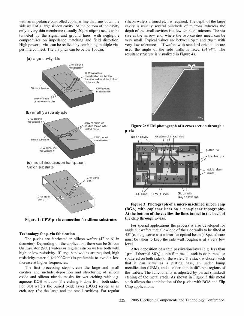
with an impedance controlled coplanar line that runs down the side wall of a large silicon cavity. At the bottom of the cavity only a very thin membrane (usually 20µm-60µm) needs to be tunneled by the signal and ground lines, with negligible compromises on impedance matching and field distortion. High power µ-vias can be realized by combining multiple vias per interconnect. The via pitch can be below 100µm.
(a) large cavity side
(b) small (via) cavity side
(c) metal structures on transparentSilicon substrate
Silicon substrate
CPW groundmetallization
CPW signal line metallization on the top,the side wall, and the bottomof the cavity
array of threeor more micro vias
CPW groundmetallization
array of mic ro viacavities sealed withplated metal
CPW groundmetallization
CPW groundmetallizationSilicon substrate
CPW signal port 1
CPW signal port 2
CPW signal linemetallization
Figure 1: CPW µ-via connection for silicon substrates
Technology for µ-via fabrication The µ-vias are fabricated in silicon wafers (4" or 6" in
diameter). Depending on the application, these can be Silicon On Insulator (SOI) wafers or regular silicon wafers both with high or low resistivity. If large bandwidths are required, high resistivity material (>4000Ωcm) is preferable to avoid a loss increase at higher frequencies.
The first processing steps create the large and small cavities and include deposition and structuring of silicon oxide and silicon nitride masks for wet etching with e.g. aqueous KOH solution. The etching is done from both sides. For SOI wafers the buried oxide layer (BOX) serves as an etch stop (for the large and the small cavities). For regular
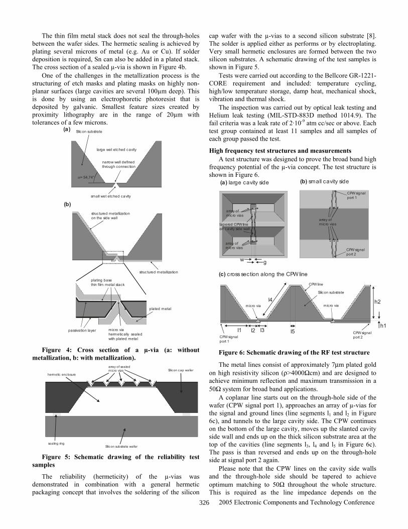
silicon wafers a timed etch is required. The depth of the large cavity is usually several hundreds of microns, whereas the depth of the small cavities is a few tenths of microns. The via size at the narrow end, where the two cavities meet, can be very small. Typical values are between 5µm and 20µm with very low tolerances. If wafers with standard orientation are used the angle of the side walls is fixed (54.74°). The resultant structure is visualized in Figure 4a.
50 µm
Figure 2: SEM photograph of a cross section through a µ-via
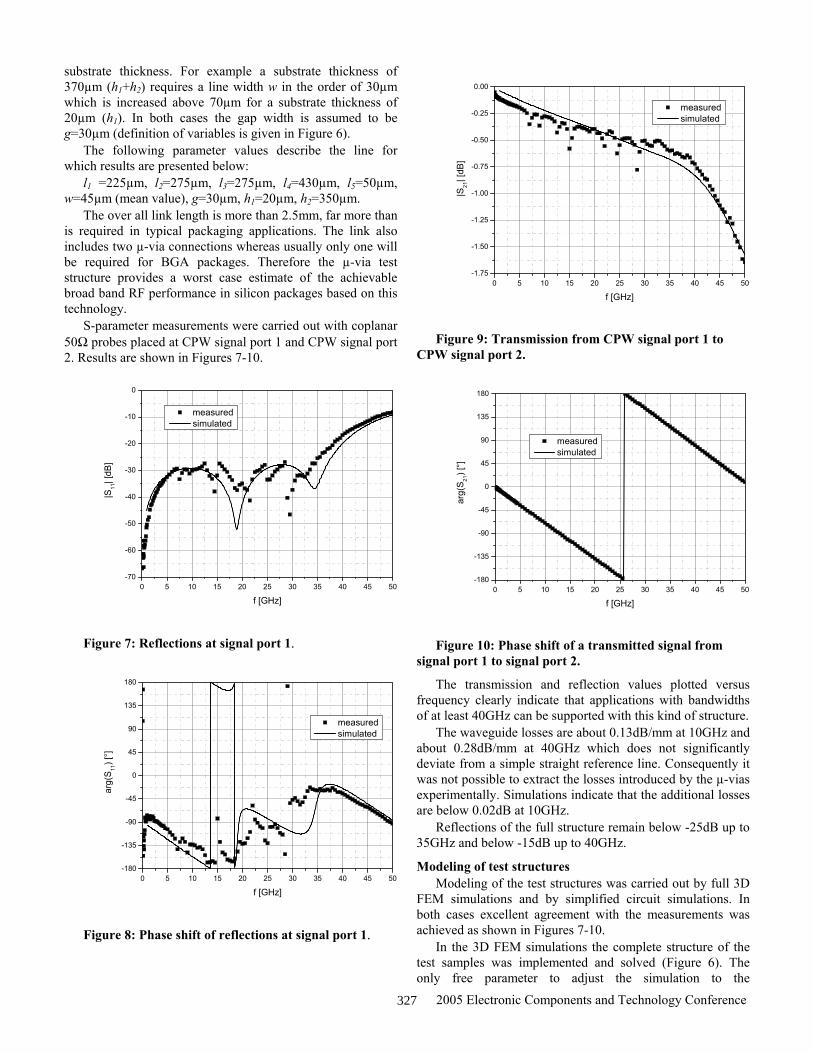
Silicon cavity
Silicon with SiO passivation2
plated Au
solder bumps
solder dammetal
CPW RF lines
location of micro vias
DC lines
Figure 3: Photograph of a micro machined silicon chip (BGA) with coplanar lines on a non-planar topography. At the bottom of the cavities the lines tunnel to the back of the chip through µ-vias.
For special applications the process is also developed for angle cut wafers that allow one of the side walls to be tilted at 45° (can e.g. serve as a mirror for optical beams). Special care must be taken to keep the side wall roughness at a very low level.
After deposition of a thin passivation layer (e.g. less than 1µm of thermal SiO2) a thin film metal stack is evaporated or sputtered on both sides of the wafer. The stack is chosen such that it can serve as a plating base, an under bump metallization (UBM), and a solder dam in different regions of the wafers. The functionality is adjusted by partial (masked) etching of the metal stack. As shown in Figure 3 this metal stack allows the combination of the µ-vias with BGA and Flip Chip applications.
325
2005 Electronic Components and Technology Conference
The thin film metal stack does not seal the through-holes between the wafer sides. The hermetic sealing is achieved by plating several microns of metal (e.g. Au or Cu). If solder deposition is required, Sn can also be added in a plated stack. The cross section of a sealed µ-via is shown in Figure 4b.
One of the challenges in the metallization process is the structuring of etch masks and plating masks on highly non-planar surfaces (large cavities are several 100µm deep). This is done by using an electrophoretic photoresist that is deposited by galvanic. Smallest feature sizes created by proximity lithography are in the range of 20µm with tolerances of a few microns.
large wet etched cavity
small wet etched cavity
Silicon substrate
struc tured metallizationon the side wall
micro viahermetically sealedwith plated metal
struc tured metallization
(a)
(b)
passivation layer
plating basethin film metal stack
plated metal
narrow well definedthrough connec tion
α= 54,74°
Figure 4: Cross section of a µ-via (a: without metallization, b: with metallization).
hermetic enc losure
array of sealedmicro vias
sealing ring
Silicon cap wafer
Silicon substrate wafer
Figure 5: Schematic drawing of the reliability test samples
The reliability (hermeticity) of the µ-vias was demonstrated in combination with a general hermetic packaging concept that involves the soldering of the silicon
cap wafer with the µ-vias to a second silicon substrate [8]. The solder is applied either as performs or by electroplating. Very small hermetic enclosures are formed between the two silicon substrates. A schematic drawing of the test samples is shown in Figure 5.
Tests were carried out according to the Bellcore GR-1221-CORE requirement and included: temperature cycling, high/low temperature storage, damp heat, mechanical shock, vibration and thermal shock.
The inspection was carried out by optical leak testing and Helium leak testing (MIL-STD-883D method 1014.9). The fail criteria was a leak rate of 2·10-9 atm cc/sec or above. Each test group contained at least 11 samples and all samples of each group passed the test.
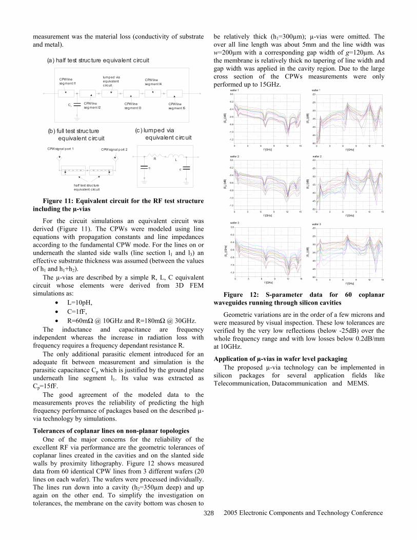
High frequency test structures and measurements A test structure was designed to prove the broad band high
frequency potential of the µ-via concept. The test structure is shown in Figure 6.
(a) large cavity side (b) small cavity side
(c) cross section along the CPW line
l1 l2
l4
l3 l5
CPW signal port 1
CPW signal port 2CPW signal
port 1
h1
h2micro viamicro via
Silicon substrate
CPW line
array of micro vias
array of micro vias
array of micro vias
w g
tapered CPW lineon cavity side wall
CPW signal port 2
Figure 6: Schematic drawing of the RF test structure
The metal lines consist of approximately 7µm plated gold on high resistivity silicon (ρ>4000Ωcm) and are designed to achieve minimum reflection and maximum transmission in a 50Ω system for broad band applications.
A coplanar line starts out on the through-hole side of the wafer (CPW signal port 1), approaches an array of µ-vias for the signal and ground lines (line segments l1 and l2 in Figure 6c), and tunnels to the large cavity side. The CPW continues on the bottom of the large cavity, moves up the slanted cavity side wall and ends up on the thick silicon substrate area at the top of the cavities (line segments l3, l4 and l5 in Figure 6c). The pass is than reversed and ends up on the through-hole side at signal port 2 again.
Please note that the CPW lines on the cavity side walls and the through-hole side should be tapered to achieve optimum matching to 50Ω throughout the whole structure. This is required as the line impedance depends on the
326
2005 Electronic Components and Technology Conference
substrate thickness. For example a substrate thickness of 370µm (h1+h2) requires a line width w in the order of 30µm which is increased above 70µm for a substrate thickness of 20µm (h1). In both cases the gap width is assumed to be g=30µm (definition of variables is given in Figure 6).
The following parameter values describe the line for which results are presented below:
l1 =225µm, l2=275µm, l3=275µm, l4=430µm, l5=50µm, w=45µm (mean value), g=30µm, h1=20µm, h2=350µm.
The over all link length is more than 2.5mm, far more than is required in typical packaging applications. The link also includes two µ-via connections whereas usually only one will be required for BGA packages. Therefore the µ-via test structure provides a worst case estimate of the achievable broad band RF performance in silicon packages based on this technology.
S-parameter measurements were carried out with coplanar 50Ω probes placed at CPW signal port 1 and CPW signal port 2. Results are shown in Figures 7-10.
0 5 10 15 20 25 30 35 40 45 50-70
-60
-50
-40
-30
-20
-10
0
|S11
| [dB
]
f [GHz]
measured simulated
Figure 7: Reflections at signal port 1.
0 5 10 15 20 25 30 35 40 45 50-180
-135
-90
-45
0
45
90
135
180
arg(
S11
) [°]
f [GHz]
measured simulated
Figure 8: Phase shift of reflections at signal port 1.
0 5 10 15 20 25 30 35 40 45 50-1.75
-1.50
-1.25
-1.00
-0.75
-0.50
-0.25
0.00
|S21
| [dB
]
f [GHz]
measured simulated
Figure 9: Transmission from CPW signal port 1 to
CPW signal port 2.
0 5 10 15 20 25 30 35 40 45 50-180
-135
-90
-45
0
45
90
135
180
arg(
S21
) [°]
f [GHz]
measured simulated
Figure 10: Phase shift of a transmitted signal from
signal port 1 to signal port 2.
The transmission and reflection values plotted versus frequency clearly indicate that applications with bandwidths of at least 40GHz can be supported with this kind of structure.
The waveguide losses are about 0.13dB/mm at 10GHz and about 0.28dB/mm at 40GHz which does not significantly deviate from a simple straight reference line. Consequently it was not possible to extract the losses introduced by the µ-vias experimentally. Simulations indicate that the additional losses are below 0.02dB at 10GHz.
Reflections of the full structure remain below -25dB up to 35GHz and below -15dB up to 40GHz.
Modeling of test structures Modeling of the test structures was carried out by full 3D
FEM simulations and by simplified circuit simulations. In both cases excellent agreement with the measurements was achieved as shown in Figures 7-10.
In the 3D FEM simulations the complete structure of the test samples was implemented and solved (Figure 6). The only free parameter to adjust the simulation to the
327
2005 Electronic Components and Technology Conference
measurement was the material loss (conductivity of substrate and metal).
CPW lineseg ment l1
CPW lineseg ment l2
lumped via equivalentc ircuit
CPW linesegment l3
CPW linesegment l4
CPW linesegment l5
Cp
(a) half test struc ture equivalent circuit
(b) full test struc ture equivalent c ircuitCPW signal port 1 CPW signal p ort 2
ha lf test struc ture equivalent c ircuit
(c ) lumped via equivalent c ircuit
c
R L
c
Figure 11: Equivalent circuit for the RF test structure including the µ-vias
For the circuit simulations an equivalent circuit was derived (Figure 11). The CPWs were modeled using line equations with propagation constants and line impedances according to the fundamental CPW mode. For the lines on or underneath the slanted side walls (line section l1 and l3) an effective substrate thickness was assumed (between the values of h1 and h1+h2).
The µ-vias are described by a simple R, L, C equivalent circuit whose elements were derived from 3D FEM simulations as:
• L=10pH, • C=1fF, • R=60mΩ @ 10GHz and R=180mΩ @ 30GHz.
The inductance and capacitance are frequency independent whereas the increase in radiation loss with frequency requires a frequency dependant resistance R.
The only additional parasitic element introduced for an adequate fit between measurement and simulation is the parasitic capacitance Cp which is justified by the ground plane underneath line segment l1. Its value was extracted as Cp=15fF.
The good agreement of the modeled data to the measurements proves the reliability of predicting the high frequency performance of packages based on the described µ-via technology by simulations.
Tolerances of coplanar lines on non-planar topologies One of the major concerns for the reliability of the
excellent RF via performance are the geometric tolerances of coplanar lines created in the cavities and on the slanted side walls by proximity lithography. Figure 12 shows measured data from 60 identical CPW lines from 3 different wafers (20 lines on each wafer). The wafers were processed individually. The lines run down into a cavity (h2=350µm deep) and up again on the other end. To simplify the investigation on tolerances, the membrane on the cavity bottom was chosen to
be relatively thick (h1=300µm); µ-vias were omitted. The over all line length was about 5mm and the line width was w=200µm with a corresponding gap width of g=120µm. As the membrane is relatively thick no tapering of line width and gap width was applied in the cavity region. Due to the large cross section of the CPWs measurements were only performed up to 15GHz.
0 3 6 9 12 15
-1.2
-1.0
-0.8
-0.6
-0.4
-0.2
0.0
|S21
|[dB
]
f [GHz]
wafer 1
0 3 6 9 12 15-50
-45
-40
-35
-30
-25
-20
|S11
|[dB
]
f [GHz]
wafer 1
0 3 6 9 12 15
-1.2
-1.0
-0.8
-0.6
-0.4
-0.2
0.0wafer 2
|S21
|[dB
]
f [GHz]0 3 6 9 12 15
-50
-45
-40
-35
-30
-25
-20
|S11
|[dB
]
f [GHz]
wafer 2
0 3 6 9 12 15-50
-45
-40
-35
-30
-25
-20
wafer 3
|S11
|[dB
]
f [GHz]
0 3 6 9 12 15
-1.2
-1.0
-0.8
-0.6
-0.4
-0.2
0.0|S
21|[
GHz
]
f [GHz]
wafer 3
Figure 12: S-parameter data for 60 coplanar waveguides running through silicon cavities
Geometric variations are in the order of a few microns and were measured by visual inspection. These low tolerances are verified by the very low reflections (below -25dB) over the whole frequency range and with low losses below 0.2dB/mm at 10GHz.
Application of µ-vias in wafer level packaging The proposed µ-via technology can be implemented in
silicon packages for several application fields like Telecommunication, Datacommunication and MEMS.
328
2005 Electronic Components and Technology Conference
pair of coplanardifferential RF lines
array of m icro viasat the cavity bottom
ICs and opticaldevices assembledin the large cavities
very short wire bonds to the cavity edge(ground and RF connections)
under bumpmetallization solder damSi/SiO2
array ofmicro vias
coplanar linewet etched cavity
ICs and opticaldevices assembledon the flat substrate side
array ofmicro vias
platedmetal
array ofmicro vias
(a)
(b)
(c)
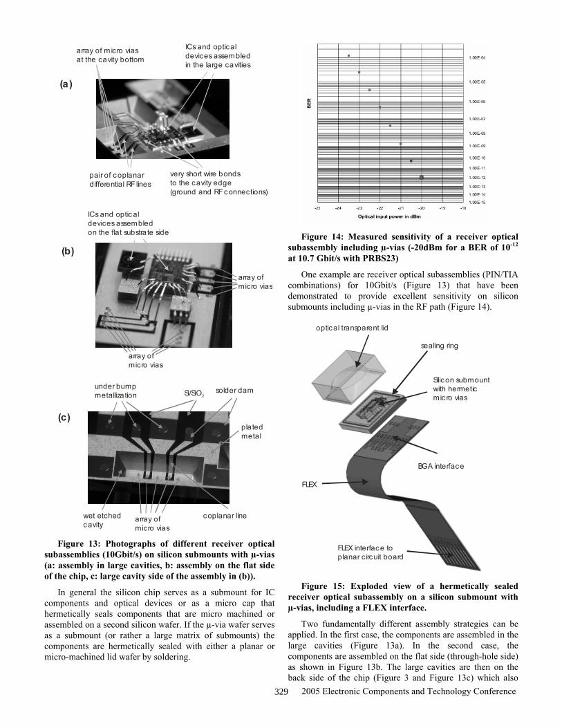
Figure 13: Photographs of different receiver optical subassemblies (10Gbit/s) on silicon submounts with µ-vias (a: assembly in large cavities, b: assembly on the flat side of the chip, c: large cavity side of the assembly in (b)).
In general the silicon chip serves as a submount for IC components and optical devices or as a micro cap that hermetically seals components that are micro machined or assembled on a second silicon wafer. If the µ-via wafer serves as a submount (or rather a large matrix of submounts) the components are hermetically sealed with either a planar or micro-machined lid wafer by soldering.
Figure 14: Measured sensitivity of a receiver optical subassembly including µ-vias (-20dBm for a BER of 10-12 at 10.7 Gbit/s with PRBS23)
One example are receiver optical subassemblies (PIN/TIA combinations) for 10Gbit/s (Figure 13) that have been demonstrated to provide excellent sensitivity on silicon submounts including µ-vias in the RF path (Figure 14).
optical transparent lid
Silicon submountwith hermetic mic ro vias
BGA interface
FLEX interface toplanar circuit board
FLEX
sealing ring
Figure 15: Exploded view of a hermetically sealed receiver optical subassembly on a silicon submount with µ-vias, including a FLEX interface.
Two fundamentally different assembly strategies can be applied. In the first case, the components are assembled in the large cavities (Figure 13a). In the second case, the components are assembled on the flat side (through-hole side) as shown in Figure 13b. The large cavities are then on the back side of the chip (Figure 3 and Figure 13c) which also
329
2005 Electronic Components and Technology Conference
serves as the interface to a circuit board or flexible circuit board.
The complete packaging concept is visualized in Figure 15 including a flexible circuit board and an optical transparent lid for sealing.
Similarly, transmitter optical subassemblies have been demonstrated both for VCSEL and edge emitter applications [9].
cap wafer
MEMS wafer
micro viafine pitchsolder connec tion
sealing ring
solder ballarrray
micro viacap wafer
(a)
(b)
(c) (d)fine pitchsolder connec tion
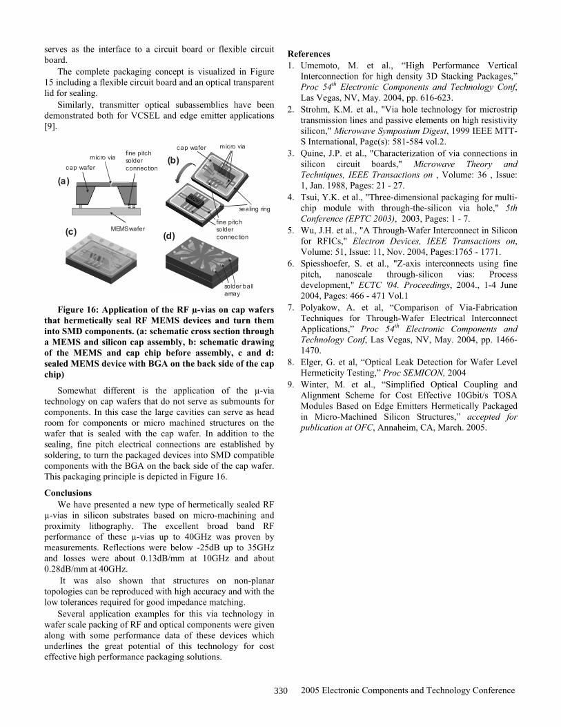
Figure 16: Application of the RF µ-vias on cap wafers that hermetically seal RF MEMS devices and turn them into SMD components. (a: schematic cross section through a MEMS and silicon cap assembly, b: schematic drawing of the MEMS and cap chip before assembly, c and d: sealed MEMS device with BGA on the back side of the cap chip)
Somewhat different is the application of the µ-via technology on cap wafers that do not serve as submounts for components. In this case the large cavities can serve as head room for components or micro machined structures on the wafer that is sealed with the cap wafer. In addition to the sealing, fine pitch electrical connections are established by soldering, to turn the packaged devices into SMD compatible components with the BGA on the back side of the cap wafer. This packaging principle is depicted in Figure 16.
Conclusions We have presented a new type of hermetically sealed RF
µ-vias in silicon substrates based on micro-machining and proximity lithography. The excellent broad band RF performance of these µ-vias up to 40GHz was proven by measurements. Reflections were below -25dB up to 35GHz and losses were about 0.13dB/mm at 10GHz and about 0.28dB/mm at 40GHz.
It was also shown that structures on non-planar topologies can be reproduced with high accuracy and with the low tolerances required for good impedance matching.
Several application examples for this via technology in wafer scale packing of RF and optical components were given along with some performance data of these devices which underlines the great potential of this technology for cost effective high performance packaging solutions.
References 1. Umemoto, M. et al., “High Performance Vertical
Interconnection for high density 3D Stacking Packages,” Proc 54th Electronic Components and Technology Conf, Las Vegas, NV, May. 2004, pp. 616-623.
2. Strohm, K.M. et al., "Via hole technology for microstrip transmission lines and passive elements on high resistivity silicon," Microwave Symposium Digest, 1999 IEEE MTT-S International, Page(s): 581-584 vol.2.
3. Quine, J.P. et al., "Characterization of via connections in silicon circuit boards," Microwave Theory and Techniques, IEEE Transactions on , Volume: 36 , Issue: 1, Jan. 1988, Pages: 21 - 27.
4. Tsui, Y.K. et al., "Three-dimensional packaging for multi-chip module with through-the-silicon via hole," 5th Conference (EPTC 2003), 2003, Pages: 1 - 7.
5. Wu, J.H. et al., "A Through-Wafer Interconnect in Silicon for RFICs," Electron Devices, IEEE Transactions on, Volume: 51, Issue: 11, Nov. 2004, Pages:1765 - 1771.
6. Spiesshoefer, S. et al., "Z-axis interconnects using fine pitch, nanoscale through-silicon vias: Process development," ECTC '04. Proceedings, 2004., 1-4 June 2004, Pages: 466 - 471 Vol.1
7. Polyakow, A. et al, “Comparison of Via-Fabrication Techniques for Through-Wafer Electrical Interconnect Applications,” Proc 54th Electronic Components and Technology Conf, Las Vegas, NV, May. 2004, pp. 1466-1470.
8. Elger, G. et al, “Optical Leak Detection for Wafer Level Hermeticity Testing,” Proc SEMICON, 2004
9. Winter, M. et al., “Simplified Optical Coupling and Alignment Scheme for Cost Effective 10Gbit/s TOSA Modules Based on Edge Emitters Hermetically Packaged in Micro-Machined Silicon Structures,” accepted for publication at OFC, Annaheim, CA, March. 2005.
330