OP-AMP and its applications
35
1 OP-AMP and its applications Introduction - The operational amplifier (Op-Amp) concept was introduced by Tellegen in 1954 under the name of “ideal amplifier”. The first Op-Amps with discrete transistors appeared in production in 1956. One of the first analog ICs was an Op-Amp developed by R. Widlar in 1964. The operational amplifier is still the integrated circuit with highest production volume. - OP-AMP is a very high-gain directly-coupled negative-feedback amplifier which can amplify signals having frequency ranging from 0 Hz to 1 MHz. - OP-AMP is so named because it was originally designed to perform mathematical operations like summation, subtraction, multiplication, differentiation integration …etc. Present day usage is much wider in scope but the popular name OP-AMP continues. nd in analog computers applications. - Typical applications of OP-AMP are scale changing, analog computer operations, in instrumentation and control systems and a great variety of phase-shift and oscillator circuits. - Example of OP-AMPs [LM 108, LM 208, 741,….] OP-AMP Circuit and Symbol Standard triangular symbol of an OP-AMP is shown in Fig.1. All OP-AMPs have a minimum of five terminals: 1. inverting input terminal (labeled with a minus sign), 2. non-inverting input terminal (labeled with a plus sign), 3. output terminal, 4. positive bias supply terminal, 5. negative bias supply terminal. Fig. 1: Operational amplifier - When an OP-AMP is operated without connecting any resistor or capacitor from its output to any one of its inputs (i.e., without feedback), it is said to be in the open-loop condition. The specifications of OP-AMP under such condition are called open-loop specifications and exhibiting the open-loop voltage gain (A OL ). - An op amp amplifies the difference between two input signals v 1 &v 2 ; i.e amplifies (v d ), where (v d =v 1 -v 2 ) v o = A OL *v d (A OL for actual op amp is extremely high i.e., about 10 6 ) However, if (v d =1 V), it does not mean that will be amplified to 10 6 V at the output. Actually, the maximum value of v o is limited by the basis supply voltage and is called its saturation voltage. This voltage is approximately 2V smaller than the power-supply voltage (V CC ). In other words, the amplifier is linear over the range -(V CC – 2) < v o < V CC - 2 , typically ± 15 V.
-
Upload
khangminh22 -
Category
Documents
-
view
2 -
download
0
Transcript of OP-AMP and its applications

1
OP-AMP and its applications Introduction
- The operational amplifier (Op-Amp) concept was introduced by Tellegen in 1954 under the
name of “ideal amplifier”. The first Op-Amps with discrete transistors appeared in production
in 1956. One of the first analog ICs was an Op-Amp developed by R. Widlar in 1964. The
operational amplifier is still the integrated circuit with highest production volume.
- OP-AMP is a very high-gain directly-coupled negative-feedback amplifier which can amplify
signals having frequency ranging from 0 Hz to 1 MHz.
- OP-AMP is so named because it was originally designed to perform mathematical operations
like summation, subtraction, multiplication, differentiation integration …etc. Present day usage
is much wider in scope but the popular name OP-AMP continues.
nd in analog computers applications.
- Typical applications of OP-AMP are scale changing, analog computer operations, in
instrumentation and control systems and a great variety of phase-shift and oscillator circuits.
- Example of OP-AMPs [LM 108, LM 208, 741,….]
OP-AMP Circuit and Symbol
Standard triangular symbol of an OP-AMP is shown in Fig.1. All OP-AMPs have a minimum
of five terminals:
1. inverting input terminal (labeled with a minus sign),
2. non-inverting input terminal (labeled with a plus sign),
3. output terminal,
4. positive bias supply terminal,
5. negative bias supply terminal.
Fig. 1: Operational amplifier
- When an OP-AMP is operated without connecting any resistor or capacitor from its output to
any one of its inputs (i.e., without feedback), it is said to be in the open-loop condition. The
specifications of OP-AMP under such condition are called open-loop specifications and
exhibiting the open-loop voltage gain (AOL).
- An op amp amplifies the difference between two input signals v1&v2; i.e amplifies (vd), where
(vd=v1-v2)
vo= AOL*vd (AOL for actual op amp is extremely high i.e., about 106)
However, if (vd=1 V), it does not mean that will be amplified to 106 V at the output.
Actually, the maximum value of vo is limited by the basis supply voltage and is called its
saturation voltage. This voltage is approximately 2V smaller than the power-supply voltage
(VCC). In other words, the amplifier is linear over the range
-(VCC – 2) < vo < VCC - 2 , typically ± 15 V.

2
Example1: An op amp has saturation voltage Vsat =10 V, an open-loop voltage gain of -105,
and input resistance of 100k. Find (a) the value of vd that will just drive the amplifier to
saturation and (b) the op amp input current at the starting of saturation.
Solution:
(a)
(b)
Ideal Operational Amplifier
An ideal OP-AMP has the following characteristics :
1. its open-loop gain AOL is infinite i.e., Aν = − ∞
2. its input resistance Ri (measured between inverting and non-inverting terminals) is infinite
i.e., Ri = ∞ Ω. This means that the input current i = 0.
3. its output resistance R0 (seen looking back into output terminals) is zero i.e., R0 = 0 Ω. This
means that v0 is not dependent on the load resistance connected across the output.
4. it has infinite bandwith i.e., it has flat frequency response from dc to infinity.
Virtual Ground and Summing Point
Fig. 2 shows an OP-AMP which employs negative feedback with the help of resistor Rf which
feeds a portion of the output to the input. The concept of virtual ground arises from the fact that
input voltage νi at the inverting terminal of the OP-AMP is forced to a small value (assumed
zero). Hence, point A is essentially at ground voltage and is referred to as virtual ground.
Obviously, it is not the actual ground.
When ν1 is applied, point A attains some positive potential and at the same time ν0 is brought
into existence. Due to negative feedback, some fraction of the output voltage is fed back to
point A antiphase with the voltage already existing there (due to ν1). The algebraic sum of the
two voltages is almost zero so that νi ≅ 0. Obviously, νi will become exactly zero when
negative feedback voltage at A is exactly equal to the positive voltage produced by ν1 at A.
Another point worth considering is that there exists a virtual short between the two terminals of
the OP-AMP because νi = 0. It is virtual because no current flows (remember i = 0) despite the
existence of this short.
Fig. 2

3
OP-AMP Applications
1- Inverting Amplifier The inverting amplifier of Fig. 3 has its noninverting input connected to ground. A signal (vin)
is applied through input resistor R1, and negative current feedback is implemented through
feedback resistor Rf . Output voltage (vo) has polarity opposite that of input.
Fig. 3
The gain of the inverting amplifier can be driven as follow:
Since point A is at ground potential (VA=0) and iin=0,
i1=i2
It is seen from above, that closed-loop gain of the inverting amplifier depends on the ratio of the
two external resistors R1 and Rf and is independent of the amplifier parameters.
2- Noninverting Amplifier The noninverting amplifier of Fig. 4 is realized by grounding R1 of Fig. 3 and applying the
input signal at the noninverting. Here, polarity of ν0 is the same as that νin.
Fig. 4

4
The gain of the noninverting amplifier can be driven as follow:
Because of virtual short between the two OP-AMP terminals, voltage across R1 is the input
voltage νin. Also, ν0 is applied across the series combination of R1 and Rf.
3- Voltage Follower It provides a gain of unity without any phase reversal. This circuit (Fig. 5) is useful as a buffer
or isolation amplifier because it allows, input voltage νin to be transferred as output voltage ν0
while at the same time preventing load resistance RL from loading down the input source. It is
due to the fact that its Ri = ∞ and R0 = 0.
Fig. 5
4- Adder or Summer Amplifier The adder circuit provides an output voltage proportional to or equal to the algebraic sum of
two or more input voltages each multiplied by a constant gain factor. It is basically similar to a
Fig. 3 except that it has more than one input. Fig. 6 shows a three-input inverting adder circuit.
As seen, the output voltage is phase-inverted.
Fig. 6

5
Calculations
As before, we will treat point A as virtual ground
Applying KCI to point A, we have

6
5- Subtractor The function of a subtractor is to provide an output proportional to the difference of two input
signals. As shown in Fig. 7. The inputs are applying at the inverting and noninverting terminals.
Fig. 7
Calculations
According to Superposition theorem;
ν0 = ν0′ + ν0″
where ν0′ is the output produced by ν1 and ν0″ is that produced by ν2.
Now (see inverting amplifier equation)
(see noninverting amplifier equation)
If Rf >> R1 and Rf/R1 >> 1, hence
Further, If Rf = R1, then
ν0 = (ν2 − ν1) = difference of the two input voltages
Example: Find the output voltages of an OP-AMP inverting adder for the following sets of
input voltages and resistors. In all cases, Rf = 1 MΩ.
ν1 = −3 V, ν2 = + 3V, ν3 = + 2V; R1 = 250 KΩ, R2 = 500 KΩ, R3 = 1 M Ω (ans. Vo=4v)
Example: In the subtractor circuit, R1 = 5 K, Rf = 10 K, ν1 = 4 V and ν2 = 5V. Find the value
of output voltage.
Solution:
Example: Design an OP-AMP circuit that will produce an output equal to − (4 ν1 + ν2 +0·1ν3).
Write an expression for the output and sketch its output waveform when ν1 = 2 sin ωt, ν2 =+5V
dc and ν3 = −100 Vdc.
Solution:
Comparing equations (1) and (2), we find,

7
Therefore if we assume Rf = 100 K, then R1 = 25 K, R2 = 100 K and R3 = 10 K. With there
values of R1, R2 and R3, the OP-AMP circuit is as shown in Fig. 8 (a).
Fig. 8
With the given values of ν1 = 2 sin ωt, ν2 = + 5V, ν3 = − 100 V dc, the output voltage,
ν0 = 2sin ωt+ 5 − 100 = 2 sin ωt − 95 V. The waveform of the output voltage is sketched as
shown in Fig.8 (b).
6- Integrator The function of an integrator is to provide an output voltage which is proportional to the
integral of the input voltage. A simple example of integration is shown in Fig. 9, where input is
dc level and its integral is a linearly-increasing ramp output. The actual integration circuit is
similar to the inverting circuit except that the feedback component is a capacitor C instead of
a resistor Rf.
Fig. 9
Calculations
As before, If the op amp is ideal, point A will be treated as virtual ground, and vin appears across
R1. Thus
1
1R
vi in

8
dt
dvc
dt
dvcii oc
c 2 (since vc=-vo)
But, with negligible current into the op amp, the current through R1 = current flow through C.
Then
dt
dvc
R
v oin 1
dtvcR
dv in
1
0
1 dtv
cRv ino
1
1
It is seen from above that output (left-hand side) is an integral of the input, with an inversion
and a scale factor of 1/CR1. This ability to integrate a given signal enables an analog computer
solve differential equations and to set up a wide variety of electrical circuit analogs of physical
system operation.
Note: we can integrate more than one input as shown below in Fig. 10. With multiple inputs,
the output is given by
Fig. 10
Example: A 5mV, 1-kHz sinusoidal signal is applied to the input of an OP-AMP integrator, for
which R = 100 K and C = 1 μF. Find the output voltage.
Solution:
7- Differentiator Its function is to provide an output voltage which is proportional to the rate of the change of
the input voltage. It is an inverse mathematical operation to that of an integrator. As shown in

9
Fig. 11, when we feed a differentiator with linearly-increasing ramp input, we get a constant dc
output.
Differentiator circuit can be obtained by interchanging the resistor and capacitor of the
integrator circuit.
Fig. 11
Calculation:
The expression for the output signal of the inverting differentiator amplifier assuming the op
amp is ideal can be derived as follows:
Taking point A as virtual ground, consequently, vin appears across capacitor (vin=vc)
dt
dvc
dt
dvci inc
dt
dvcRR
dt
dvciRvv inin
Ro
As seen, output voltage is proportional to the derivate of the input voltage, the constant of
proportionality (i.e., scale factor) being (−RC).
Example: The input to the differentiator circuit is a sinusoidal voltage of peak value of 5 mV
and frequency 1 kHz. Find out the output if R = 1000 K and C = 1 μF.
Solution
The equation of the input voltage is ν1 = 5 sin 2 π × 1000 t = 5 sin 2000 πt mV
scale factor = CR = 10−6 × 10
5 = 0·1
dt (5 sin 2000 πt) = (0·5 × 2000 π) cos 2000 πt = 1000 π cos 2000 πt mV
As seen, output is a cosinusoidal voltage of frequency 1 kHz and peak value 1000 π mV.
8- Comparator
It is a circuit which compares two signals or voltage levels. The circuit is the simple because it
needs no additional external components shown in Fig. 12. If ν1 and ν2 are equal, then ν0
should ideally be zero.
Fig. 12
Output of the comparator can be summarized as follows
If V1>V2 then Vo=-Vcc (Vsat)
If V1<V2 then Vo=Vcc (Vsat)

10
Fig. 13

11
Application of comparator
1- Zero Crossing Detector Comparator can be used as a zero crossing detector. A typical circuit for such a detector is
shown below:
Fig. 14
During the positive half-cycle, the input voltage is positive, hence the output voltage is +Vsat .
During the negative half-cycle, the input voltage is negative, hence the output voltage is -Vsat .
Thus the output voltage switches between +Vsat and -Vsat whenever the input signal crosses
the zero level.
Fig. 15
Looking at the waveform shown above, we realize that a zero crossing detector can be used as a
sine- to square-wave converter. This is an impractical circuit, since any noise on the input
waveform near the zero crossings will cause multiple level transitions in the output signal
(cause a comparator to erratically switch output states). In order to make the comparator less
sensitive to noise, a comparator with positive feedback, called hysteresis, can be used. This
comparator is called Schmitt trigger.
2- Output Bounding (or Voltage limiter)
In some applications, it is necessary to limit the output voltage levels of a comparator to a value
less than the saturation voltage. A single zener diode can be used, as shown in Fig. 16, to limit
the output voltage to the zener voltage in one direction and to the forward diode voltage drop in
the other. This process of limiting the output range is called bounding.
The operation is as follows. Since the anode of the zener is connected to the inverting input, it is
at virtual ground Therefore, when the output voltage reaches a positive value equal to the zener
voltage, it limits at that value, as illustrated in Figure 17(a). When the output switches negative,
the zener acts as a regular diode and becomes forward-biased at 0.7 V, limiting the negative
output voltage to this value, as shown in part (b). Turning the zener around limits the output
voltage in the opposite direction.

12
Fig. 17-(a) Bounded at a positive value
Fig. 17-(b) Bounded at a negative value
Two zener diode connected back to back with a comparator as in Fig. 18 to limit the output
voltage to the zener voltage plus the voltage drop (0.7V) of the forward bias zener diode, both
positively and negatively.
Fig. 18
9- Logarithmic and Antilog Amplifier
Log and antilog amplifiers are used in applications that require compression of analog
input data, linearization of transducers that have exponential outputs, and analog multiplication
and division. They are often used in high-frequency communication systems, including fiber
optics, for processing wide dynamic range signals.
Note: The logarithm of a number is the power to which the base must be raised to get that
number. A logarithmic (log) amplifier produces an output that is proportional to the logarithm
of the input, and an antilogarithmic (antilog) amplifier takes the antilog or inverse log of the
input.
a- Logarithmic Amplifier
The logarithmic amplifier is the use of a feedback-loop device that has an exponential terminal
characteristic curve (diode or BJT transistor) which is characterized by
TDTD VV
R
VV
RD eIeII//
)1( …….(1)
Where IR is reverse leakage current, ID is the forward diode current, VD is the forward diode
voltage (approximately 0.7 V), VT is the thermal voltage and is a constant equal to
approximately 25 mV at 25Co.

13
Fig. 19
An analysis of the circuit in Figure 19 is as follows, beginning with the facts that:
Din
in IR
VI ………(2)
and VD=-Vo ……….(3)
Substituting into the formula of eq. 1,
Tout VV
Rin eI
R
V /
TVoutV
eRIV Rin
/
Take the natural logarithm (ln ) of both sides
T
outRin
VV
RinV
VRIVeRIV Tout
)ln()ln()ln()ln(
/
……..(4)
R
inTinRTout
RI
VVVRIVV ln)]ln()[ln( ……. (5)
Under the condition that the term RIR is negligible (which can be accomplished by controlling R
so that RIR ≈ 1, where the factor,IR, is a constant for a given diode), then gives Vout ≈ -VT ln (Vin).
Note: ln is the natural logarithm to the base e. A natural logarithm is the exponent to which
the base e must be raised in order to equal a given quantity. Although eq. 5 will use natural
logarithms in the formulas, each expression can be converted to a logarithm to the base
10(log10) using the relationship ln x = 2.3 log10x.
Example: Determine the output voltage for the log amplifier in Fig. 19. Assume IR = 50nA and
R=100k.
Solution:
Note1: The output voltage of the logarithmic amplifier is limited to a maximum value of
approximately (-0.7V).
Note2: The input must be positive when the diode is connected in the direction shown in the
Fig. 19. To handle negative inputs, the diode must be reversed.
Log Amplifier with a BJT The base-emitter junction of a bipolar junction transistor exhibits the same type of logarithmic
characteristic as a diode because it is also a pn junction. A log amplifier with a BJT connected
in a common-base form in the feedback loop is shown in Figure 20. Notice that Vout with
respect to ground is equal to -VBE.

14
Fig. 20
The analysis for this circuit is the same as for the diode log amplifier except that VBE replaces
VD, IC replaces ID and IBEO replaces IR. The expression for the VBE versus IC characteristic curve
is
TBE VV
EBOC eII/
where IEBO is the emitter-to-base leakage current. The expression for the output voltage is
)ln(RI
VVV
EBO
inTout
b- Antilog Amplifier
The antilogarithm of a number is the result obtained when the base is raised to a power equal
to the logarithm of that number. To get the antilogarithm, you must take the exponential of the
logarithm (antilogarithm of x=elnx
).
An antilog amplifier is formed by connecting a transistor (or diode) as the input element as
shown in Fig. 21. The exponential formula still applies to the base-emitter pn junction. The
output voltage is determined by the current (equal to the collector current) through the feedback
resistor.
Vout = -Rf IC
The characteristic equation of the pn junction is
TBE VV
EBOC eII/
Substituting into the equation for Vout
TBE VV
EBOfout eIRV/
As you can see in Fig. 21, Vin = VBE
Tin VV
EBOfout eIRV/
The exponential term can be expressed as an antilogarithm as follows:
)log(T
inEBOfout
V
VantiIRV
Where VT is approximately 25 mV.
Fig. 21

15
Example: For the antilog amplifier in Figure 21, find the output voltage. Assume IEBO = 40 nA,
Vin=175.1 mV and Rf= 68k.
solution
Note: In certain applications, a signal may be too large in magnitude for a particular system to
handle. In these cases, the signal voltage must be scaled down by a process called signal
compression so that it can be properly handled by the system. If a linear circuit is used to scale
a signal down in amplitude, the lower voltages are reduced by the same percentage as the higher
voltages. Linear signal compression often results in the lower voltages becoming obscured by
noise and difficult to accurately distinguish, as illustrated in Fig. 22-a. To overcome this
problem, a signal with a large dynamic range can be compressed using a logarithmic response,
as shown in Figure 22-b. In logarithmic signal compression, the higher voltages are reduced by
a greater percentage than the lower voltages, thus keeping the lower voltage signals from being
lost in noise.
Fig. 22 ++++++++++++++++++++++++++++++++++++++++++++++++++++++++++++++++++++
Questions
1. What purpose does the diode or transistor perform in the feedback loop of a log amplifier?
2. Why is the output of a log amplifier limited to about 0.7 V?
3. What are the factors that determine the output voltage of a basic log amplifier? 4. In terms of implementation, how does a basic antilog amplifier differ from a basic log amplifier?
5. Define the term bounding in relation to a comparator’s output.
6. What is the reference voltage for each comparator in Figure 23?
Fig. 23

16
Other OP-AMP Circuts This section introduces other op-amp circuits that represent basic applications of the op-
amp. These circuit, of course, not a comprehensive coverage of all possible op-amp circuits but
is intended only to introduce some common basic uses.
1- Constant Current Source
A constant-current source delivers a constant current to the load even the load resistance
changes. Figure 24 shows a basic circuit in which a voltage source (VIN) provides a constant
current (Ii) through the input resistor (Ri).
Since the inverting input of the op-amp is at virtual ground (0V), the value of (Ii) is
determined by
Now, since Ii = IL
If RL changes, IL remains constant as long as VIN and Ri are held constant.
Fig. 24
2- Precision Rectifiers
Rectifier circuits can be implemented with silicon junction diodes. Recall that for the
diode to conduct, the voltage across it must be ≈ 0.7 V. Therefore, a major limitation of these
circuits is that they cannot rectify voltages below about 0.7 V. In addition, since the input
voltage has to rise to about 0.7 V before any appreciable change can be seen at the output, the
output is distorted as shown in Fig. 25.
Fig. 25
- half-wave rectifier (HWR) is a circuit that passes only the positive (or only the negative)
portion of a wave, while blocking out the other portion. The transfer characteristic of the
positive HWR is:
vO = vi for vi > 0 , vO = 0 for vi < 0.
- full-wave rectifier (FWR), besides passing the positive portion, inverts and then passes also
the negative portion. Its transfer characteristic is:
vO = vi for vi > 0 , vO = vi for vi < 0. or, more concisely, vO = |vi |

17
i- Half-Wave Rectifiers
Figure 26 below shows a precision half-wave rectifier circuit consisting of a diode placed
in the negative-feedback path of an ideal op-amp.
Fig. 26
The analysis of the circuit of Fig. 26 above is illustrated as below:
1- when input voltage is positive (vi > 0), the op-amp output (v) will also positive, turning ON
the diode and thus creating the negative-feedback path shown in Fig. 27-a. This allows op amp
to operate as voltage follower and give vO = vi (prove that). The output of the op amp (v) is a
diode drop above vO, (v = vO + VD(on)) ≈ vO + 0.7 V.
2- when input voltage is negative (vi < 0): The op amp output (v) is negative, turning the diode
OFF and thus causing the current through R to go to zero. Hence, vO =0. As shown in Fig. 27-b,
the op amp is now operating in the open-loop mode.
Fig. 27
A disadvantage of this circuit is that when vi changes from positive to negative the op-
amp will be saturated close to its negative supply rail. Thus, the op amp output may exhibit
intolerable distortion. The improved HWR of Fig. 28 alleviates this inconvenience by using a
second diode. Circuit operation is summarized as:
1- vi > 0 vO = 0. (positive input causes D1 to conduct, thus creating a negative-feedback path
around the op amp. By the virtual-ground, D1 now clamps the op amp output at v = −VD1(on) ≈
−0.7 V. Moreover, D2 is OFF, so no current flows through R2 and, hence, vO = 0).
2- vi < 0 vO = vi . (negative input causes the op amp output positive, thus turning D2 ON.
This creates an alternative negative-feedback path via D2 and R2. Clearly, D1 is now OFF, so the
op amp operate as inverting amplifier, i.e. vO = (−R2/R1)vi).
Fig. 28

18
Full-Wave Rectifiers
There are many configuration for achieving precision FWR. One of them is given in Fig. 29.
Here op amp (OA1) provides inverting half-wave rectification, and op amp (OA2) sums vi and
the HWR output (vHW) to give vO = −[(R5/R4)vi + (R5/R3)vHW].
Where vHW = −(R2/R1)vi for vi > 0, and vHW = 0 for vi < 0.
Fig. 29

19
Example1: Draw the output showing its proper relationship to the input signal of the
comparator circuit shown in Fig.30. Assume the maximum output levels of the op-amp are ±
12V.
Fig.30
Solution:
When Vin > 0 Vout =+12 (maximum positive level)
When Vin > 0 Vout =-12 (maximum negative level)
Fig. 40
Example2: Draw the output showing its proper relationship to the input signal of the
comparator circuit shown in Fig.41. Assume the maximum output levels of the op-amp are
±12V.
Fig.41
Solution:
The reference voltage (VREF) is set by R1 and R2 (use voltage divider rule)
As shown in Fig. 42, each time the input exceeds +1.63 V, the output voltage switches to its
+12V level, and each time the input goes below +1.63 V, the output voltage switches to its -
12V level.

20
Fig. 42
Problem: Draw the output showing its proper relationship to the input signal of the comparator
circuits shown in Fig.43. Assume the maximum output levels of the op-amp are ± 15V.
Fig. 43
Example3: Determine the output voltage response to the input square wave for the ideal
integrator in Fig. 44. The output voltage is initially zero.
Fig. 44
Solution
The output voltage during the time that the input is at +2.5 V (capacitor charging) is
The output voltage during the time that the input is negative (capacitor discharging) is the same
as during charging except it is positive.

21
When the input is at +2.5 V, the output is a negative-going ramp. When the input is at -2.5V the
output is a positive-going ramp.
During the time the input is at +2.5 V, the output is a negative-going ramp (will go from 0 to -
5). During the time the input is at -2.5V the output is a positive-going ramp (will go from -5 V
to 0 V). Therefore, the output is a triangular wave with peaks at 0 and -5 as shown in Fig. 45.
Fig. 45
Example: Determine the output voltage of the ideal op-amp differentiator in Fig.46 for the
triangular-wave input shown.
Fig.46
Solution
Starting at t= 0, the input voltage is a positive-going ramp ranging from -5V to +5V (+10V
change) in 5μs. Then it changes to a negative-going ramp ranging is:
Time constant = R C = (2.2 kΩ) (0.001 μF) = 2.2 μs
And sVs
V
t
V
dt
dV inin
/2)05(
)55(
Vdt
dVRCV in
out 4.422.2
Likewise, the slope of the negative-going ramp is -2V/μs and the output voltage is VVout 4.4)22.2(
Figure 47 shows a graph of the output voltage waveform relative to the input.
Fig. 47

22

23

24

25

26

27
Digital to Analog conversion
It is an important interface process for converting digital signals to analog signals. An
example is a voice signal that is digitized for storage, processing, or transmission and must be
changed back into an approximation of the original audio signal in order to drive a speaker.
The R/2R ladder is more commonly method used for D/A conversion because it requires only
two resistor values as shown in Fig. 48 for four bits.
Fig. 48
Assume that the D3 input is HIGH (+5 V) and the others are LOW (ground, 0 V). This
condition represents the binary number 1000. A circuit analysis will show that this reduces to
the equivalent form shown in Fig. 49 (a).
Essentially no current goes through the 2R equivalent resistance (REQ) because the inverting
input is at virtual ground. Thus, all of the current (I=5/2R) through R7 is also through Rf, and
the output voltage is -5V.
Figure (b) shows the equivalent circuit when the D2 input is at +5 V and the others are at
ground. This condition represents 0100. If we thevenize looking from R8, we get 2.5 V in series
with R, as shown. This results in a current through Rf of I= 2.5/2R, which gives an output
voltage of -2.5V. Keep in mind that there is no current from the op-amp inverting input and that
there is no current through R7 because it has 0 V across it, due to the virtual ground.

28
Figure (c) shows the equivalent circuit when the D1 input is at +5 V and the others are at
ground. This condition represents 0010. Again thevenizing looking from R8, you get 1.25 V in
series with R as shown. This results in a current through Rf of I= 1.25 V/2R, which gives an
output voltage of -1.25.
In Fig. (d), the equivalent circuit representing the case where D0 is at +5 V and the other inputs
are at ground is shown. This condition represents 0001. Thevenizing from R8 gives an
equivalent of 0.625 V in series with R as shown. The resulting current through Rf is
I=0.625V/2R, which gives an output voltage of -0.625 V.
Notice that each successively lower-weighted input produces an output voltage that is halved,
so that the output voltage is proportional to the binary weight of the input bits.
In summary, We can prove that the equivalent analog voltage shown in Fig. 50 below is
obtained from the relation:
((The proof is left as an exercise))
Where (n) is the number of digital inputs.

29
Fig.50
Figure 51 shows a four−bit R−2R ladder network and an op−amp connected to form a DAC.
The op amp shown is an inverting amplifier and in this case the reference voltage (Vref) should
be negative so that the amplifier output will be positive. Alternately, a non−inverting op amp
could be used with a positive value of (Vref)
Example: Figure 52 shows a four−bit DAC where all four switches are set at the ground level.
Find the analog voltage value at the output of the unity gain amplifier for each of the sets of the
switch positions shown in Table. Fill−in the right−most column with your answers.
Fig. 52
30
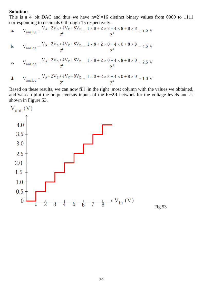
Solution:
This is a 4−bit DAC and thus we have n=24=16 distinct binary values from 0000 to 1111
corresponding to decimals 0 through 15 respectively.
Based on these results, we can now fill−in the right−most column with the values we obtained,
and we can plot the output versus inputs of the R−2R network for the voltage levels and as
shown in Figure 53.
Fig.53

31
Active Filters
A filter circuit can be constructed using passive components like resistors and capacitors. But
an active filter, in addition to the passive components makes use of an OP-AMP as an amplifier.
The amplifier in the active filter circuit may provide voltage amplification and signal isolation
or buffering. There are four major types of filters namely, low-pass filter, high-pass filter, and
band-pass filter and band-stop filter. All these four types of filters are discussed in the following
sections.
1- low−pass filter transmits (passes) all frequencies from dc or zero frequency up to a critical
(cutoff) frequency denoted as wc, and attenuates (blocks) all frequencies above this cutoff
frequency. An op amp low−pass filter is shown in Figure 54(a &b) and its amplitude frequency
response in Figure 54(c).
In Figure 54(c), the blue lines represent the ideal characteristics and the smooth curve represents
the practical characteristics, where the gain does not reduce immediately to zero. The vertical
scale represents the magnitude of the ratio of output to input voltage Vout/Vin, that is, the gain
Av.
The cutoff frequency wc is the frequency at which the maximum value of Vout/Vin falls to
0.707Cv , and this is called the half power or the -3dB point.
2- high−pass filter passes all frequencies above a cutoff frequency wc , and blocks all
frequencies below the cutoff frequency. An op amp high−pass filter is shown in Figure 55(a&b)
and its frequency response in Figure 55(c).

32
3- band−pass filter passes the band (range) of frequencies between the cutoff frequencies
denoted as w1 and w2, where the maximum value of Av which is unity, falls to 0.707Cv, while it
blocks all frequencies outside this band. A simple way to construct a band-pass filter is to
cascade a low-pass filters and a high-pass filter as shown in Figure 56(a) and its frequency
response in Figure 56(b). The values of w1 and w2 can be obtained by using the relations, 1/R1C1
and, 1/ R2 C2. Then band width,
BW = w2 − w1
And the centre frequency,
W0=w1w2
The Quality-factor (or Q-factor) of the band pass filter circuit.
Q=W0/BW

33
Fig 56
4- band−elimination or band−stop or band−rejection filter attenuates (rejects) the band of
frequencies between the critical (cutoff) frequencies denoted as w1 and w2, where the maximum
value of Cv which is unity, falls to 0.707Cv, while it passes all frequencies outside this band. An
op amp band−stop filter is shown in Figure 57(a) and its frequency response in Figure 57(b).
The block diagram shows that the circuit is made up of a high-pass filter, a low-pass filter and a
summing amplifier. The summing amplifier produces an output that is equal to a sum of the
filter output voltages. The circuit is designed in such a way so that the cut-off frequency, w1
(which is set by a low-pass filter) is lower in value than the cut-off frequency, w2 (which is set
by high-pass filter). The gap between the values of w1 and w2 is the bandwidth of the filter.
When the circuit input frequency is lower than w1, the input signal will pass through low-pass
filter to the summing amplifier. Since the input frequency is below the cut-off frequency of the
high pass filter, V2 will be zero. Thus the output from the summing amplifier will equal the
output from the low-pass filter. When the circuit input frequency is higher than w2, the input
signal will pass through the high-pass filter to the summing amplifier. Since the input frequency
is above the cut-off frequency of the low-pass filter, V1 will zero. Now the summing amplifier
output will equal the output from the high-pass filter.

34
Butterworth Filter There are many different types of active filters. Among the most useful of them are Butterworth
filters because they have an excellent response. Butterworth filters, named after British engineer
Stephen Butterworth.
Table-1 below gives the Butterworth polynomials for n up to 8. Note that for n even, the
polynomials are the products of quadratic forms, and for n odd, there is present the additional
factors (s+1).
…….(1)
And

35
Example: design a fourth-order Butterworth low-pass filter with a cutoff frequency of 1kHz.
Solution
we cascaded two second-order prototypes as given below.
Exercise: design a third-order Butterworth low-pass filter with a cutoff frequency of 10kHz.