NR LATEX COATED NANO ZnO DISKS FOR POTENTIAL DIELECTRIC APPLICATIONS
10
Journal of Optoelectronics and Biomedical Materials Vol. 6, Issue 4, October - December 2014 p. 101 - 110 NR LATEX COATED NANO ZnO DISKS FOR POTENTIAL DIELECTRIC APPLICATIONS D. THOMAS a , b* , S. AUGUSTINE b , J. PRAKASH c a Research and Development Centre, Bharathiar University, Coimbatore, India- 641046 b Research and Post-Graduate Department of Physics, St.Thomas College, Pala, Kottayam, India-686574 c Research and Post-Graduate Department of Chemistry, St.Thomas College, Pala, Kottayam, India-686574 The present study focuses on the synthesis of ZnO nanoparticles of varying size (40- 100nm) by reverse micelle method using sodium dodecyl sulphide as stabilising agent. The variation in size was obtained by changing the calcination temperature. The nanocrystalline nature of the prepared samples was investigated using different techniques such as UV-Visible spectrophotometer, IR spectrometer, XRD, SEM, TEM. The prepared powder samples were then pressed into disks and coated with natural rubber (NR latex) using dip coating technique. The dielectric studies of the nano ZnO- rubber disks were then carried out at varying frequencies. The effect of particle size on dielectric constant, dielectric loss, ac conductivity and Q factor was examined. It was found that all the parameters are very sensitive to the size of the particle. The parameters can be tuned to desired values by varying the particle size. The Particles calcinated at 550°C, having minimum size, show the most promising results. (Received September 1, 2014; Accepted October 13, 2014) Keywords: ZnO powder SDS Calcination Temperature Nano ZnO rubber disks 1. Introduction The research on semiconductor nanostructures has great importance in recent years due to their optical, electrical and photocatalytic properties. The unique properties of semiconductor nanostructures are due to quantum effects and increased surface to volume ratio [1]. The different semiconducting nanomaterials of single elements, compound semiconductors and metal oxides have been successfully synthesized and studied. For the last few decades, ZnO has attracted much interest due to its versatile properties such as transparency in the visible range, direct band gap (3.37 eV), large exciton binding energy of 60 meV, absence of toxicity, etc. These qualities make it the best candidate for applications like transparent conducting electrodes in flat panel displays and window layers in solar cells [2-4]. It also exhibits many potential applications in areas such as laser diodes, solar cells, gas sensors, optoelectronic devices [5–7]. The ZnO nanoparticles can be synthesized using various techniques such as hydrothermal [8], sol–gel [9], wet chemical [10], precipitation [11], microemulsion [12], chemical vapor deposition [13], solid state reaction [14] and laser ablation [15]. The dielectric properties of an insulating medium can be modified by dispersing electrically conducting particles in the medium [16–19]. Thus the insulating host material can be modified into conducting or semi-conducting depending on the amount of filler particles dispersed in the medium [20- 22]. Zinc oxide is one of the most important basic components of rubber compounds. In rubber processing, it acts as an activator for the cross linking by sulphur or sulphur donors [23]. The rubber industry, utilized optical, physical and chemical properties of ZnO. It is the most effective activator to speed up the rate of cure. It can improve * Corresponding author:[email protected]
Transcript of NR LATEX COATED NANO ZnO DISKS FOR POTENTIAL DIELECTRIC APPLICATIONS

Journal of Optoelectronics and Biomedical Materials Vol. 6, Issue 4, October - December 2014 p. 101 - 110
NR LATEX COATED NANO ZnO DISKS FOR POTENTIAL DIELECTRIC
APPLICATIONS
D. THOMASa , b*, S. AUGUSTINEb, J. PRAKASHc
aResearch and Development Centre, Bharathiar University, Coimbatore, India-
641046
bResearch and Post-Graduate Department of Physics, St.Thomas College, Pala,
Kottayam, India-686574
cResearch and Post-Graduate Department of Chemistry, St.Thomas College, Pala,
Kottayam, India-686574
The present study focuses on the synthesis of ZnO nanoparticles of varying size (40-
100nm) by reverse micelle method using sodium dodecyl sulphide as stabilising agent.
The variation in size was obtained by changing the calcination temperature. The
nanocrystalline nature of the prepared samples was investigated using different techniques
such as UV-Visible spectrophotometer, IR spectrometer, XRD, SEM, TEM. The prepared
powder samples were then pressed into disks and coated with natural rubber (NR latex)
using dip coating technique. The dielectric studies of the nano ZnO- rubber disks were
then carried out at varying frequencies. The effect of particle size on dielectric constant,
dielectric loss, ac conductivity and Q factor was examined. It was found that all the
parameters are very sensitive to the size of the particle. The parameters can be tuned to
desired values by varying the particle size. The Particles calcinated at 550°C, having
minimum size, show the most promising results.
(Received September 1, 2014; Accepted October 13, 2014)
Keywords: ZnO powder SDS Calcination Temperature Nano ZnO rubber disks
1. Introduction
The research on semiconductor nanostructures has great importance in recent years due to
their optical, electrical and photocatalytic properties. The unique properties of semiconductor
nanostructures are due to quantum effects and increased surface to volume ratio [1]. The different
semiconducting nanomaterials of single elements, compound semiconductors and metal oxides
have been successfully synthesized and studied. For the last few decades, ZnO has attracted much
interest due to its versatile properties such as transparency in the visible range, direct band gap
(3.37 eV), large exciton binding energy of 60 meV, absence of toxicity, etc. These qualities make it
the best candidate for applications like transparent conducting electrodes in flat panel displays and
window layers in solar cells [2-4]. It also exhibits many potential applications in areas such as
laser diodes, solar cells, gas sensors, optoelectronic devices [5–7]. The ZnO nanoparticles can be
synthesized using various techniques such as hydrothermal [8], sol–gel [9], wet chemical [10],
precipitation [11], microemulsion [12], chemical vapor deposition [13], solid state reaction [14]
and laser ablation [15]. The dielectric properties of an insulating medium can be modified by
dispersing electrically conducting particles in the medium [16–19]. Thus the insulating host
material can be modified into conducting or semi-conducting depending on the amount of filler
particles dispersed in the medium [20- 22]. Zinc oxide is one of the most important basic
components of rubber compounds. In rubber processing, it acts as an activator for the cross linking
by sulphur or sulphur donors [23]. The rubber industry, utilized optical, physical and chemical
properties of ZnO. It is the most effective activator to speed up the rate of cure. It can improve
*Corresponding author:[email protected]

102
the resistance to corona effects by its dielectric strength in high-voltage wire and cable insulation.
The materials properties such as melting points, mechanical properties, and electrical properties
change at nanoscale. The studies on the effect of frequency on the dielectric behaviour and a.c
electrical conductivity give useful information about the conduction phenomenon in
nanostructured materials. It was also noted that premelting of samples greatly depend upon the ac
conductivity. And also the premelting of the mixtures at higher temperature led to a somewhat
higher enhancement in ac conductivity because these temperatures are not high enough to allow
for sintering or forming agglomerates [24]. The dielectric properties of particles are due to the
contributions from electronic, ionic, dipolar and space charge polarizations. The determination of
dielectric properties of the material is also important to assess the usability of the material in
various electronic and optoelectronic applications.
In this work, the ZnO nanoparticles of different sizes were fabricated using the cost
competitive and simple reverse micelle technique. In order to reduce the agglomeration among the
smaller particles, the sodium dodecyl sulphide molecule which can bind to the surface of
nanoparticles in the initial nucleation stage is used. Different samples were prepared by varying
the calcination temperature. The ZnO nanoparticles are then characterised using UV-Visible
spectrophotometer, IR spectrometer, Scanning electron microscope, transmission electron
microscope and XRD. It was found that particle size increases with calcination temperature. So in
order to find out the optimum temperature a TGA-DTA analysis of the sample was done. The
prepared particles are then pressed into round disks of 1cm diameter and thickness 2mm. The disks
were then coated with natural latex rubber using a microcontrolled dip coating unit. The dielectric
properties of prepared nano ZnO-natural rubber disks are studied at room temperature.
2. Experimental
The ZnO nanoparticles were prepared by reverse micelle method. In a typical experiment,
first solution was prepared by dissolving 8.636 g ZnSO4. 3.603 g CH3COOH and 40 mg SDS as
surfactant in 1 dm3 of water. The second solution was prepared by 3.6gNaOH pellets and 25ml
70% of ethanol. Then the first solution was slowly added to the second solution with continuous
stirring. The obtained precipitate was filtered by using a Whatmann filter (grade-41) and air dried.
The white solid product was washed with ethanol six times and with water ten times to remove
impurities. Then, the dried precipitate was divided into four portions. The four portions were
calcinated at 200 0C, 9000C, 7500C, and 5500C for one hour respectively. The samples were named
as, A, B, C, D. The obtained powders were characterized using XRD, UV-Visible absorption
Spectroscopy, FTIR, TEM and SEM. The TGA analysis of Zn(OH)2 was carried out using a TA
instrument (SDT-2960) thermogravimetric analyser. The FTIR spectra were obtained using a
SHIMADZU FTIR-8400S Japan in the range of 400 cm−1 to 5000 cm−1. The UV-Visible spectra of
ZnO nano particle suspended in deionised water were recorded using an analytic Jena (Specord
50) spectrophotometer. X-ray diffractograms of ZnO nano powders were taken using a GE
Inspection Technologies Seifert (PTS 3003) using a copper kα radiation (λ=1.54A). Scanning
electron micrographs of ZnO nano particles were obtained by (Philips XL 30) SEM. Transmission
electron micrographs were taken in a JEOL Crop. (JEM – 3010) TEM microscope at an
accelerating voltage of 100KV.
The samples were then made into disks of 1cm diameter and 2mm thickness. The disks
were coated with a 0.5mm layer of natural rubber using dip coating technique.
2.1 Dielectrical studies
These studies were carried out using a Hioki LCR Impedence analyzer (model 3532-50) in
the frequency range of 100 KHz to 5MHz, at room temperature. The samples were inserted
between two copper plates of the same diameter to form a capacitor in a home-made dielectric cell
whose fabrication details are reported elsewhere [25]. Using the impedance analyzer, the
capacitance and loss tangent were measured at different intervals using an automated measurement
set-up.

103
3. Results and discussion
3.1 Thermogravimetric analysis
A Thermogram of Zn(OH)2 heated from room temperature to 800°C in nitrogen
atmosphere is shown in fig. 1. It is clearly seen in the curves that the mass loss begins just below
200°C and the rate of mass loss increases with increasing in temperature up to 500°C, after which
the mass becames constant. The constant mass indicates that all the Zn(OH)2 has been converted
into ZnO.
Fig. 1. Thermogram of Zn(OH)2
3.2 Spectroscopic analysis
3.2.1 FTIR spectroscopy
The fig. 2a, 2b, 2c and 2d show the FTIR spectra of ZnO powders heat treated at 200°C,
550°C, 750°C, and 900°C. For the powders heat treated at 900°C only the band due to the Zn-O
bond at 500 cm -1 is seen. IR spectra of powders heat treated at 550°C show bands near 1517cm-1
(C = O stretching mode), 2339cm-1 (due to the adsorption of CO2 from atmosphere on the metallic
cation and a band at 500cm-1 (Zn-O) . The IR spectra of powder heat treated at 200°C shows many
strong bands. This shows that Zn(OH)2 does not change completely into ZnO. The intensity and
position of the band near 500 cm-1 is similar in all cases, indicating that temperature will not affect
the Zn-O bond.
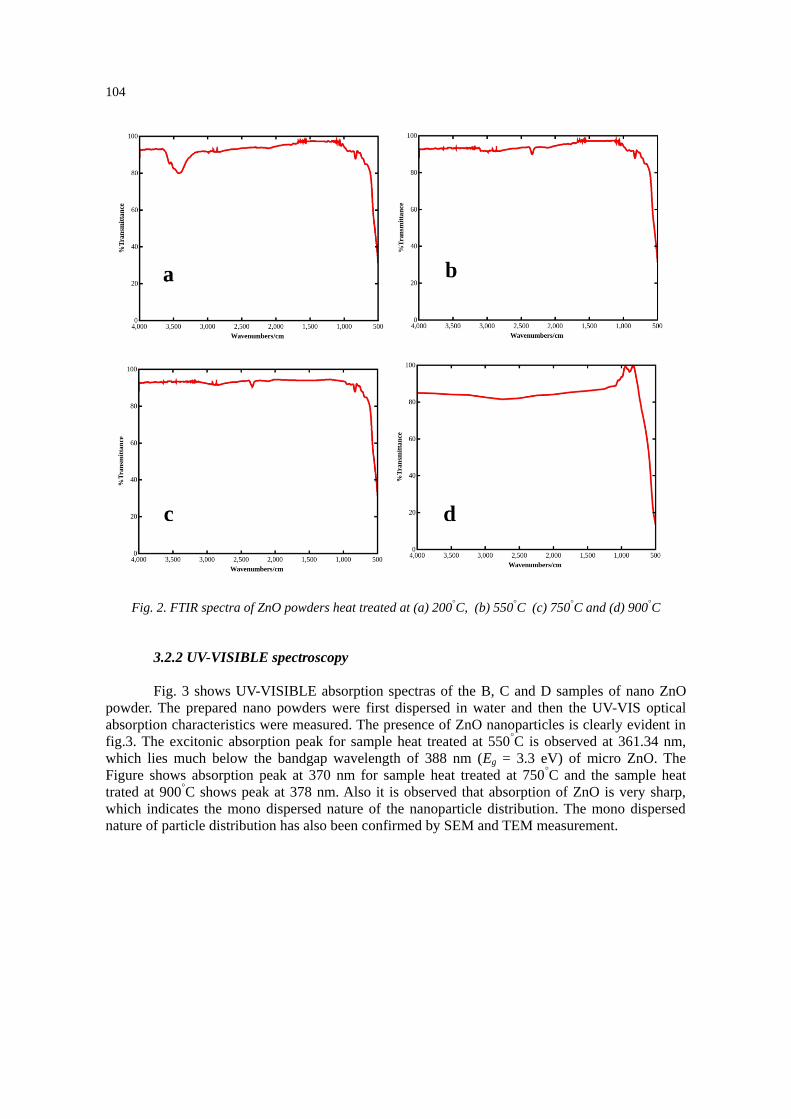
104
Fig. 2. FTIR spectra of ZnO powders heat treated at (a) 200°C, (b) 550°C (c) 750°C and (d) 900°C
3.2.2 UV-VISIBLE spectroscopy
Fig. 3 shows UV-VISIBLE absorption spectras of the B, C and D samples of nano ZnO
powder. The prepared nano powders were first dispersed in water and then the UV-VIS optical
absorption characteristics were measured. The presence of ZnO nanoparticles is clearly evident in
fig.3. The excitonic absorption peak for sample heat treated at 550°C is observed at 361.34 nm,
which lies much below the bandgap wavelength of 388 nm (Eg = 3.3 eV) of micro ZnO. The
Figure shows absorption peak at 370 nm for sample heat treated at 750°C and the sample heat
trated at 900°C shows peak at 378 nm. Also it is observed that absorption of ZnO is very sharp,
which indicates the mono dispersed nature of the nanoparticle distribution. The mono dispersed
nature of particle distribution has also been confirmed by SEM and TEM measurement.

105
Fig. 3. UV-VISIBLE absorption spectra of nano ZnO powder at various temperatures
Only the largest particles contribute to the absorbance, at the absorption edge. But in case
of the smaller wavelength range, particles with smaller sizes contribute more. At the region of
absorbance maximum, all particles contribute to the absorbance. Thus the average particle size
present in a nano colloid can be obtained from the inflection point in the uv spectrum. Equation (1)
based on the effective mass model, gives the relation between the particle size (r, radius) and the
peak absorbance wavelength (λp) for mono dispersed ZnO nano colloid. ZnO nano particles
prepared at 5500C show peak absorbance at ~361 nm which corresponds to average particle size of
52.34 nm.
(nm)λ+
(nm)λ++
=r(nm)
p
p
2483.26.3829
10240.7226.230120.3049
(1)
3.3 XRD studies
Fig. 4 shows XRD patterns of nano ZnO crystals. The broadening in the XRD peaks
reveals the nanocrystalline nature of the particles. The broadening of the peaks decreases with
increasing calcinations temperature showing that size increases with increase in temperature. X ray
diffraction patterns are obtained when incident X-rays are scattered by the parallel planes in the
particles. As the powder size decreases, the planes in them rearrange so that the number of parallel
planes decreases. Because of this the peaks broadens. The particle size was calculated using the
Scherer equation, D = 0.9λ / βcosθ where D is the particle size, λ is the wavelength, β is the full
width at half maximum and θ is the diffraction angle. X ray difractograms of nano ZnO calcinated
at various temperatures shows a maximum intense peak is at the 2θ value 36.2° and d (interplannar
distance) value 2.48056 indicates hexagonal crystal structure of ZnO and this peak broadens with
decrease in particle size. As the calcination temperature increased from 200°C to 900°C the size of
the particles increased from 22nm to 66nm. As mentioned earlier, the formation of ZnO is
incomplete at 200o C.

106
Fig. 4. X ray diffraction patterns of ZnO heat treated at various temperatures
3.3.1 Effect of calcination temperature on metal oxide nanoparticles
The fig. 5 shows variation of average particle size of powders with different calcination
temperatures. The particle size increases with increase in calcination temperature. The XRD
studies and SEM micrographs clearly show this. SEM shows that the shape changes from spherical
to hexagonal. The size of the crystal is proportional to its surface energy, hence small crystals get
converted into large crystals automatically. The process happens immeadetly, especially at high
temperature. The process becomes complete with prolonged calcination time. The crystal size
increases with the calcination temperatures [26] . And it leads to the acquisition of large size
nanoparticles .
Fig. 5. variation of particle size with calcination temperature (obtained from XRD data)

107
3.4 Microscopic analysis
3.4.1 Scanning electron microscopy
The scanning electron micrographs of nanocrystalline ZnO powders are shown in figure 6.
As seen in the figure, the powder calcined at 900°C (fig. 6a) has hexagonal structure and the
particles have size in the range of a few hundred nanometres. As we decrease the temperature, it
can be seen that the size decreases and the shape changes from hexagonal to almost spherical. At
550°C (fig. 6b) the size is around 40 nm and at 200°C (fig. 6c) the size is around 20 nm. The size
obtained from scanning electron micrographs is in agreement with size obtained from XRD.
Fig. 6. SEM micrographs of nano ZnO (a) at 900°C (b) at 550°C and (c) at 200°C
3.4.2 Transmission Electron microscopy
The formation of the metal oxide nanoparticles can be easily proved by Transmission
electron microscopy. Fig. 7 shows TEM images recorded from drop coated films of the ZnO nano
particles prepared by calcination at 550°C. The particles are mono disperse in nature with an
average size of 40-60nm. The nanoparticles are predominantly spherical in shape. Fig. 7a and 7b
both include a scale for comparison.

108
Fig. 7. TEM Micrographs of ZnO nanoparticles.
3.5 Dielectric Studies
The electrical properties of a dielectric substance are usually described in terms of
dielectric constant and dielectric loss. The variation of dielectric constant as function of frequency
at room temperature of samples A, B, C and D is shown in the figure 8a. The dielectric constant or
relative permittivity is determined using the equation εr= C.d/ ε0A, where C is the capacitance of
the sample, d and A are the thickness and area of the sample pellet. The figure 8a shows the
variation of dielectric constant with frequency at room temperature. It is clear from the results that
the dielectric constant remains fairly constant at higher frequencies. Here dielectric constant
decreases with the increasing frequency for all the samples. At lower frequency (100 KHz), this
effect is more prominent. Increase in dielectric constant in nano ZnO–rubber disks is nearly
inversely with the particle size of the ZnO particles. In this case sample D possesses more
dielectric constant compared to other samples, but the sample A dielectric constant is low because
of the incomplete formation of ZnO. The space charge effect will be a prominent factor, in
determining the dielectric properties in materials with small particle sizes [27, 28]. In addition, ion
jump polarization may also be greater in nanocrystalline materials since there will be a number of
positions at the grain boundaries for the ions to occupy. The high values of the dielectric constant
in the present study may be attributed to the increased ion jump orientation effect and the
increased space charge effect exhibited by nanoparticles. The variations of dielectric loss factor
(tanδ) of samples A, B, C, and D with different frequency are shown in figure 8b. It can be seen
that the dielectric loss shows the behaviour similar to that of the dielectric constant. In dielectric
materials, dielectric losses usually occur due to absorption current. In nanophase materials,
inhomogeneities like defects and space charge formation in the interphase layers produce an
absorption current resulting in a dielectric loss. Hence It is possible to obtain a desired dielectric
constant in conjunction with small dielectric loss. The samples are thus potential candidates for
making capacitors [26]. With the addition of a rubber coating to assure mechanical integrity, the
disk becomes a practical candidate for capacitor manufacture. The a.c conductivity of the samples
was calculated using the equation. σac=2πfε0εrtanδ [22] and shown in the figure 8c, where f is the
frequency, ε0 is the permittivity of free space, εr is the relative permittivity of the sample and tanδ
is the dielectric loss factor. The ac conductivity increases with increase in frequency. The a.c.
conductivities strongly depend on the particle size, the concentration and heat treatment of the
sample and the premelting of the electrolytes [24]. It can be seen that σac increases with frequency
for samples A, B, C and D in a sequential order. Here a.c conductivity of sample D is few orders

109
higher than the other samples. The increase of a.c. conductivity with the frequency indicates that
the mobility of charge carriers is responsible for hopping [29]. The electrons which are involved in
hopping are responsible for the electronic polarization in nano ZnO rubber disks.
3.5.1 Q – Factor
The Q-factor of samples is measured in the frequency range of 100 KHz to 5 MHz The
Fig. 8d explains the plot of Q-factor versus frequency of nano ZnO-rubber disks ,i.e. Sample A, B,
C, and D. It can be seen that Q-factor increases with frequency for all the samples. For the sample
A Q- factor is much low compared to other samples.
Fig. 8. (a) Variation of dielectric constant with Log f, (b) Variation of dielectric loss with Log f
(c) Variation of ac conductivity with Log f (d) Variation of Q- Factor with Log f
4. Conclusion
In the present study ZnO nanopowders were synthesised successfully with sodium dodecyl
sulphide as the stabilising agent. The monodisperse nano size of the prepared particles was
confirmed by different characterising techniques. In this investigation the direct relationship of
particle size with calcination temperature was well established. The dielectric studies of the rubber
coated disks prepared from the nano ZnO particles of different size were carried out. It was found
that the dielectric properties vary with paricle size. By changing the particle size we can tune the
dielectric parameters to the desired value. This finding permits the fabrication of electronic and
optoelectronic devices with improved characteristics. The high value of dielectric constant for
nano ZnO-natural rubber disks enhances its property towards nanoscale charge storage devices
which is an essential prerequisite for biomedical applications.

110
Acknowledgment
The authors are grateful to Prof. Mike Raleigh, retired physicist from Pennsylvania State
University USA, 16802, for the valuable help he rendered regarding the manuscript.
Reference
[1] G. Shan, X. Kong, X. Wang, Y. Liu. Surf. Sci. 582, 61 (2005).
[2] Z.L. Wang. J. Physics:Condensed Matter. 16, 829 (2004).
[3] Z. Fan , J.G. Lu. J. Nanoscience and Nanotechnology. 5(10), 1561 (2005).
[4] S. Baruah, J. Dutta. Sci. Technol. Adv. Mater. 10(1), (2009).
[5] D. S. Mao, X. Wang, W. Li, X. H. Liu, Q. Li, J. F. Xu. J. Vac. Sci. Technol. B. 20, 278 (2002).
[6] Y. W. Zhu, H. Z. Zhang, X. C. Sun, S. Q. Feng, J. Xu, Q. Zhao, B. Xiang, R. M. Wang and D.
P. Yu. Appl. Phys. Lett. 83. 144 (2003).
[7] W.Z. Wang, B.Q. Zeng, J. Yang, B. Poudel, J.Y. Huang, M.J. Naughton and Z.F. Ren.
Adv.Mater. 18, 3275 (2006).
[8] A. Rabenau, Angew. Chem. Int. Ed. Engl. 24, 1026 (1985).
[9] J. Huang, N. Matsunaga, K. Shimanoe, N. Yamazoe, T. Kunitake. Chem. Mater.
17, 3513 (2005).
[10] A. Yadav, V. Prasad, A. Kathe, S. Raj, D. Yadav, C. Sundaramoorthy, N. Vigneshwaran. Bull.
Mater. Sci. 29, 641 (2006).
[11] N. Izu, N. Murayama, W. Shin, T. Itoh, I. Matsubara. Mater. Lett. 62(2), 313 (2008).
[12] Y. Liu, C. Zheng, W. Wang, C. Yin, G. Wang, Adv. Mater., 13, 1883 (2001).
[13] Y. K. Liu, C. L. Zheng, W. Z. Wang, Y. J. Zhan, G. G. Wang, J. Cryst. Growth.
233, 8 (2001).
[14] C. K. Xu, G. D. Xu, Y. K. Liu, X. L. Zhao, G. H. Wang. Scripta Mater. 46, 789 (2002).
[15] D. F. Zhang, L. D. Sun, J. L. Yin, C. H. Yan. Adv. Mater. 15, 1022 (2003) .
[16] T. Tanaka, G.C. Montanari, R. Mulhaupt. IEEE Trans. Dielect. Electr. Insul. II.
11(5), 763 (2004).
[17] G. M. Tsangaris, G. C. Psarras, A. J. Kontopoulos. J. Non-Cryst. Solids. 131, 1164 (1991).
[18] G. C. Psarras, E. Manolakaki, G. M. Tsangaris. Composites Part A. 33, 375 (2002).
[19] G. C. Psarras, Composites Part A . 37(10), 1545 (2006).
[20] P. S. Neelakanta. Handbook of Electromagnetic Materials, CRC Press, (1995).
[21] B. Zhang, Y. Feng, J. Xiong, Y. Yang, H. Lu. IEEE Trans. Magn. 42(7), 1778 (2006).
[22] S. Sindhu, M.R. Anantharaman, B.P. Thampi, K. A. Malini, P. Kurian. Bull. Mater.Sci.
25 (7), 599 (2002).
[23] F. W. H. Kruger , W. J. Mc Gill. J. Appl.Polym Sci. 42, 2643 (1991).
[24] K. Shah1, J. B. Wagner. J. Solid State Chemistry. 42, 107 (1982).
[25] E. Muhammad Abdul Jamal, P. A. Joy, P. Kurian, M. R. Anantharaman, Materials Science
and Engineering B,156, 24 (2009). [26] L. E. Shi, X. J Fang, Z. L Zhang, T. Zhou, D. Jiang, H. Wu, Z. X. Tang. Int. J. Food Sci.
Tech., 47, 1866 (2012).
[27] Y. P. Xu, W. Y. Wang, D. F. Zhang, X. L. Chen. J. Mater. Sci. 36, 4401 (2001).
[28] W. Y. Wang, Y. P. Xu, D. F. Zhang, X. L. Chen. Mater. Res. Bull. 36, 2155 (2001).
[29] T. Moumit Ghosh, C. N .R. Rao, Chem. Phys. Lett. 393, 493 (2004).