Photonic crystal and photonic wire nano-photonics based on silicon-on-insulator
Upload
independentCategory
view
1download
0
Novel All-Optical Logic Gates Based on Photonic Crystal Structure
This article has been downloaded from IOPscience. Please scroll down to see the full text article.
2012 J. Phys.: Conf. Ser. 350 012007
(http://iopscience.iop.org/1742-6596/350/1/012007)
Download details:
IP Address: 157.193.6.32
The article was downloaded on 03/11/2012 at 13:08
Please note that terms and conditions apply.
View the table of contents for this issue, or go to the journal homepage for more
Home Search Collections Journals About Contact us My IOPscience

Novel All-Optical Logic Gates Based on Photonic Crystal
Structure
Mortaza Noshad1,2
, Amin Abbasi2, Reza Ranjbar
2,* Reza Kheradmand
2
1 Faculty of Electrical and Computer Engineering, University of Tabriz, Tabriz, Iran
2 Research Institute for Applied Physics and Astronomy, University of Tabriz, Tabriz,
Iran
*Corresponding Email: [email protected]
Abstract. We have designed AND, NOT, and NOR logic gates based on photonic crystal
structure employing cross-waveguide geometry with nonlinear rods using finite difference time
domain (FDTD) method. The logical function is based on the frequency resonance shift of the
microcavity caused by Kerr nonlinearity. The proposed devices benefit a simple and small
structure, and clear operating principle.
1. Introduction
Photonic crystal (PhC) is a promising candidate as a platform on which to construct devices with
dimensions of a few wavelengths of light for future photonic integrated circuits. The photonic crystal
concept was proposed in 1987 [1,2], and the first 3D experimental photonic crystal with full band gap
was manufactured in 1991. The existence of band gap in PhC structures led to many prominent
applications in integrated optics. Photonic crystals are nowadays used for different applications such
as filters [3], modulators [4–6], switches [7], beam splitters [8-10], and super prisms [11–13] for
multiplexing and demultiplexing for example.
All-optical switching is one of the most important targets for photonics. However, this goal has been
considered difficult to achieve because of the inefficiency of optical nonlinearity in materials. All-
optical switching utilizes the nonlinear refractive-index change as a function of the electrical field
intensity.
Nonlinear photonic crystal microcavities offer unique fundamental ways of enhancing a variety of
nonlinear optical processes for optical switching. When ultrasmall and high-quality factor cavities are
used as switches, the field is enhanced by Q/V, where V is the mode volume. By taking into account
the reduction of frequency shift required for switching by a factor of Q, cavities will generally exhibit
a switching power reduction scaled as V/Q2 [14].
Ultra-compact all-optical logic gates are advanced kinds of optical switches which are used as key
elements for real-time optical processing and information communications. As a consequence of
recent advantages in nanophotonic fabrication, the amount of compactness and low loss of photonic
crystal (PC) structures make them one of the best candidates for constructing ultra-fast optical
integrated circuits. So far, several schemes have been investigated to realize various all-optical logic
functions such as AND, NOT, NOR, XOR, NAND gates [15-20].
In this paper, we have proposed novel all optical AND, NOT, and NOR gate based on cross-
waveguide geometry using nonlinear 2D photonic crystal lattice. The prominent features of these gates
in comparison to the former designed gates are their fast switching action (about 10 ps), and structure
compactness (it has the dimensions in the order of several wavelengths of light). In addition, since the
International Symposium on Optics and its Applications (OPTICS2011) IOP PublishingJournal of Physics: Conference Series 350 (2012) 012007 doi:10.1088/1742-6596/350/1/012007
Published under licence by IOP Publishing Ltd 1
same structure has the compatibility to be used as AND, NOT, and NOR gates it offers good
candidates for all-optical integrated circuits in contrast to previously designed gates [15-20].
Numerical assessment for the bistable switching action in this geometry has been discussed earlier in
[21].
2. Design and Simulation
In this work a 2D photonic crystal lattice with nonlinear rods is used. The structure is based on a 15 ×
15 square lattice with the lattice constant a = 575 nm. The material used for fabrication of nonlinear
rods is AlGaAs which provides the refractive index of 3.5 with instantaneous Kerr coefficient of n2 =
1.5×10⁻¹⁷
W/m2. In addition, the background material is taken to be air with refractive index of 1. The
radius of the rods is set to 0.2a. As shown in figure 1, two cross waveguides are created by elimination
of the rows of rods. These are connected to each other using a asymmetric cavity. Since the radiuses of
the elliptical cavity have been taken different, so, we will have two separate modes in the vertical and
horizontal directions. The cavity is considered to have the radiuses ra = 0.27a and rb = 0.32a. This
geometry provides the resonance wavelengths of 1550 nm in X-direction, and 1649 in Y-direction.
Only TM modes are considered in the paper, it is well known that Maxwell‟s equations can be
described in scalar forms for TM modes as
( )yz
HEr
x t
(1)
( )z xE Hr
y t
(2)
( )y x z
H H Er
x y t
(3)
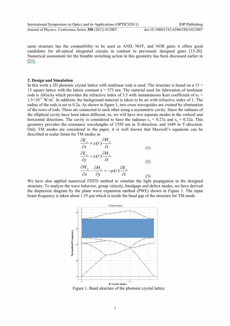
We have also applied numerical FDTD method to simulate the light propagation in the designed
structure. To analyze the wave behavior, group velocity, bandgaps and defect modes, we have derived
the dispersion diagram by the plane wave expansion method (PWE) shown in Figure 1. The input
beam frequency is taken about 1.55 µm which is inside the band gap of the structure for TM mode.
Figure 1. Band structure of the photonic crystal lattice
International Symposium on Optics and its Applications (OPTICS2011) IOP PublishingJournal of Physics: Conference Series 350 (2012) 012007 doi:10.1088/1742-6596/350/1/012007
2

Figure 2 shows the general structure for proposed logic gates.
Figure 2. General structure for proposed logic gates
I) AND Gate
Firstly we discuss the AND gate design using this structure. AND gate encompasses of two inputs and
an output. As shown in table 1 the output is logically „1‟ if and only if both of the input values are „1‟.
Table 1. Logic table of AND gate
A B Output
0 0 0
0 1 0
1 0 0
1 1 1
In this gate we use the input signals A and B (No signal is applied via Input C in this case). We take
the frequency of signal A such that normally it does not match with the resonance frequency of cavity.
So, the output power in this case is about zero. By applying the input signal B, the resonance
frequency will change, and signal A fall at the resonance frequency of cavity. As the result, the output
power reaches to about 90% of the input power A. Figure 3 demonstrates the resonance frequency
shift of the cavity. ωc and ωI represent the cavity resonance and input signal A frequencies
respectively. The resonance frequency shift in cavity causes the output power change. For the input B
field amplitude of 450 V/m, the resonance wavelength shift is about 5.7 nm. We have taken the
amplitude of input signal A so small that it makes no effective influence in resonance shift. Note that
existence of both signals A and B are necessary for making nonzero output power. Thus the system
performs as an AND gate.
International Symposium on Optics and its Applications (OPTICS2011) IOP PublishingJournal of Physics: Conference Series 350 (2012) 012007 doi:10.1088/1742-6596/350/1/012007
3
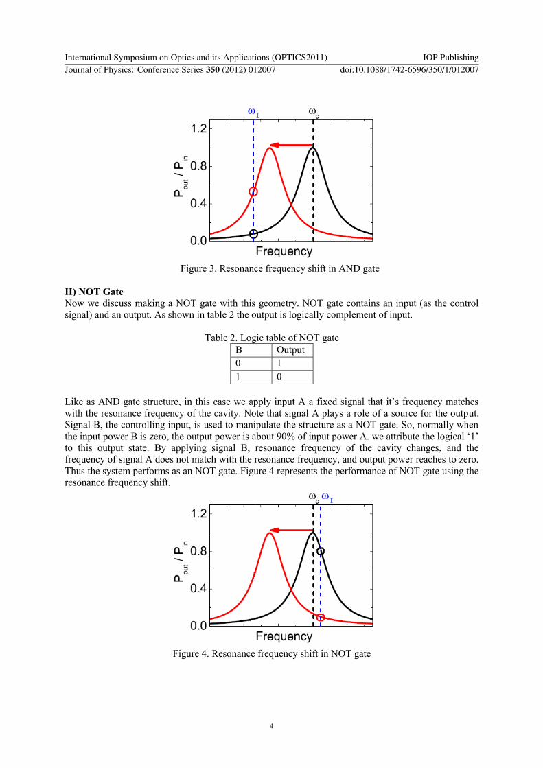
Figure 3. Resonance frequency shift in AND gate
II) NOT Gate
Now we discuss making a NOT gate with this geometry. NOT gate contains an input (as the control
signal) and an output. As shown in table 2 the output is logically complement of input.
Table 2. Logic table of NOT gate
B Output
0 1
1 0
Like as AND gate structure, in this case we apply input A a fixed signal that it‟s frequency matches
with the resonance frequency of the cavity. Note that signal A plays a role of a source for the output.
Signal B, the controlling input, is used to manipulate the structure as a NOT gate. So, normally when
the input power B is zero, the output power is about 90% of input power A. we attribute the logical „1‟
to this output state. By applying signal B, resonance frequency of the cavity changes, and the
frequency of signal A does not match with the resonance frequency, and output power reaches to zero.
Thus the system performs as an NOT gate. Figure 4 represents the performance of NOT gate using the
resonance frequency shift.
Figure 4. Resonance frequency shift in NOT gate
International Symposium on Optics and its Applications (OPTICS2011) IOP PublishingJournal of Physics: Conference Series 350 (2012) 012007 doi:10.1088/1742-6596/350/1/012007
4
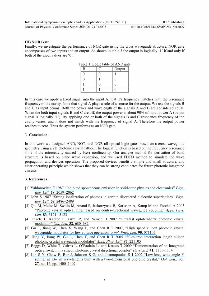
III) NOR Gate
Finally, we investigate the performance of NOR gate using the cross waveguide structure. NOR gate
encompasses of two inputs and an output. As shown in table 3 the output is logically „1‟ if and only if
both of the input values are „0‟.
Table 1. Logic table of AND gate
B C Output
0 0 1
0 1 0
1 0 0
1 1 0
In this case we apply a fixed signal into the input A, that it‟s frequency matches with the resonance
frequency of the cavity. Note that signal A plays a role of a source for the output. We use the signals B
and C as input beams. Both the power and wavelength of the signals A and B are considered equal.
When the both input signals B and C are off, the output power is about 90% of input power A (output
signal is logically „1‟). By applying one or both of the signals B and C resonance frequency of the
cavity varies, and it does not match with the frequency of signal A. Therefore the output power
reaches to zero. Thus the system performs as an NOR gate.
3. Conclusion
In this work we designed AND, NOT, and NOR all optical logic gates based on a cross waveguide
geometry using a 2D photonic crystal lattice. The logical function is based on the frequency resonance
shift of the microcavity caused by Kerr nonlinearity. Our analyze method for derivation of band
structure is based on plane wave expansion, and we used FDTD method to simulate the wave
propagation and devices operation. The proposed devices benefit a simple and small structure, and
clear operating principle which shows that they can be strong candidates for future photonic integrated
circuits.
3. References
[1] Yablonovitch E 1987 “Inhibited spontaneous emission in solid-state physics and electronics” Phys.
Rev. Lett. 58, 2059–2062
[2] John S 1987 “Strong localization of photons in certain disordered dielectric superlattices” Phys.
Rev. Lett. 58, 2486–2489
[3] Qiu M, Mulot M, Swillo M, Anand S, Jaskorzynak B, Karlsson A, Kamp M and Forchel A 2003
“Photonic crystal optical filter based on contra-directional waveguide coupling” Appl. Phys.
Lett. 83, 5121– 5123
[4] Fekete L, Kadlec F, Kuzel P, and Nemec H 2007 “Ultrafast optoterahertz photonic crystal
modulator” Opt. Lett. 32, 680–682
[5] Gu L, Jiang W, Chen X, Wang L, and Chen R T 2007, “High speed silicon photonic crystal
waveguide modulator for low voltage operation” Appl. Phys. Lett. 90, 071105
[6] Jiang Y, Jiang W, Gu L, Chen T, and Chen R T 2005 “80-micron interaction length silicon
photonic crystal waveguide modulator” Appl. Phys. Lett. 87, 221105
[7] Beggs D, White T, Cairns L, O‟Faolain L, and Krauss T 2009 “Demonstration of an integrated
optical switch in a silicon photonic crystal directional coupler” Physica E 41, 1111–1114
[8] Lin S Y, Chow E, Bur J, Johnson S G, and Joannopoulos S J 2002 “Low-loss, wide-angle Y
splitter at 1.6-_m wavelengths built with a two-dimensional photonic crystal,” Opt. Lett., vol.
27, no. 16, pp. 1400–1402
International Symposium on Optics and its Applications (OPTICS2011) IOP PublishingJournal of Physics: Conference Series 350 (2012) 012007 doi:10.1088/1742-6596/350/1/012007
5

[9] Takeda H and Yoshino K 2003 “Tunable light propagation in Y-shaped waveguides in two-
dimensional photonic crystals utilizing liquid crystals as linear defects,” Phys. Rev. B, vol. 67, p.
073106
[10] Inoue K, Sugimoto Y, Ikeda N, Tanaka Y, Asakawa K, Sasaki H, and Ishida K 2004 “Ultra-small
photonic-crystal-waveguide-based Y-splitters useful in the near-infrared wavelength region,”
Jpn. J. Appl. Phys., vol. 43, no. 4A, pp. L 446–L 448
[11] Kosaka H, Kawashima T, Tomita A, Notomi M, Tamamura T, Sato T, and Kawakami S 1998
“Superprism phenomena in photonic crystals” Phys. Rev. B 58, R10096
[12] Amet J, Baida F, Burr G, and Bernal M.-P 2008 “The superprism effect in lithium niobate
photonic crystals for ultra-fast, ultra-compact electro-optical switching” Photonic. Nanostruct.
6, 47–59
[13] Diziain S, Amet J, Baida F I, and Bernal M.-P 2008 “Optical far-field and near-field observations
of the strong angular dispersion in a lithium niobate photonic crystal superprism designed for
double (passive and active) demultiplexer applications” Appl. Phys. Lett. 93, 261103
[14] Tanabe T, Notomi M, Mitsugi S, Shinya A, and Kuramochi E 2005 “All-optical switches on a
silicon chip realized using photonic crystal nanocavities,” Appl. Phys. Lett. 87(15), 151112
[15] FragaW B, Menezes J W M, Silva M G, Sobrinho C S and Sombra A S B 2006 All optical logic
gates based on an symmetric nonlinear directional coupler Opt. Commun. 262 32
[16] Igarashi K and Kikuchi K 2008 Optical signal processing by phase modulation and subsequent
spectral filtering aiming at applications to ultrafast optical communication systems IEEE J. Sel.
Top. Quantum Electron. 14 551
[17] Wu Y D, Shih T T and Chen M H 2008 New all-optical logic gates based on the local nonlinear
Mach–Zehnder interferometer Opt. Express 16 248
[18] Pereira S, Chak P and Sipe J E 2003 All-optical AND gate by use of a Kerr nonlinear
microresonator structure Opt. Lett.28 444
[19] Li Z, Chen Z and Li B 2005 Optical pulse controlled all-optical logic gates in SiGe/Si multimode
interference Opt. Express13 1033
[20] Fujisawa T and Koshiba M 2006 All-optical logic gates based on nonlinear slot-waveguide
couplers J. Opt. Soc. Am. B 23 684
[21] Yanik M F, Fan S, Soljacic M, Joannopoulos J D 2003 "All-optical transistor action with bistable
switching in a photonic crystal crosswaveguide geometry", Opt. Lett. 28, 2506-2508
International Symposium on Optics and its Applications (OPTICS2011) IOP PublishingJournal of Physics: Conference Series 350 (2012) 012007 doi:10.1088/1742-6596/350/1/012007
6
Copyright © 2022 FDOKUMEN