NKK-HUST Kiến trúc máy tính Thiết kế bộ xử lý theo kiến trúc MIPS
74
NKK-HUST Kiến trúc máy tính Thiết kế bộ xử lý theo kiến trúc MIPS Nguyễn Kim Khánh Trường Đại học Bách khoa Hà Nội Jan2015 Computer Architecture - MIPS 1
-
Upload
independent -
Category
Documents
-
view
3 -
download
0
Transcript of NKK-HUST Kiến trúc máy tính Thiết kế bộ xử lý theo kiến trúc MIPS

NKK-HUST
Kiến trúc máy tính
Thiết kế bộ xử lý theo kiến trúc MIPS Nguyễn Kim Khánh Trường Đại học Bách khoa Hà Nội
Jan2015 Computer Architecture - MIPS 1

NKK-HUST
1. Thực hiện bộ xử lý MIPS cơ bản 2. Thiết kế khối datapath 3. Thiết kế control unit 4. Kỹ thuật đường ống lệnh
Nội dung
Jan2015 Computer Architecture - MIPS 2

NKK-HUST
1. Thực hiện bộ xử lý MIPS cơ bản
n Xem xét hai cách thực hiện bộ xử lý theo kiến trúc MIPS: n Phiên bản đơn giản n Phiên bản được đường ống hóa (gần với thực tế)
n Chỉ thực hiện với một số lệnh cơ bản của MIPS, nhưng chỉ ra hầu hết các khía cạnh: n Các lệnh tham chiếu bộ nhớ: lw, sw n Các lệnh số học/logic: add, sub, and, or, slt n Các lệnh chuyển điều khiển: beq, j
Jan2015 Computer Architecture - MIPS 3

NKK-HUST
Tổng quan quá trình thực hiện các lệnh
n Hai bước đầu tiên với mỗi lệnh: n Đưa địa chỉ từ bộ đếm chương trình PC đến
bộ nhớ lệnh, tìm và nhận lệnh từ bộ nhớ này n Sử dụng các số hiệu thanh ghi trong lệnh để
chọn và đọc một hoặc hai thanh ghi: n Lệnh lw: đọc 1 thanh ghi n Các lệnh khác (không kể lệnh jump): đọc 2 thanh
ghi
Jan2015 Computer Architecture - MIPS 4
NKK-HUST
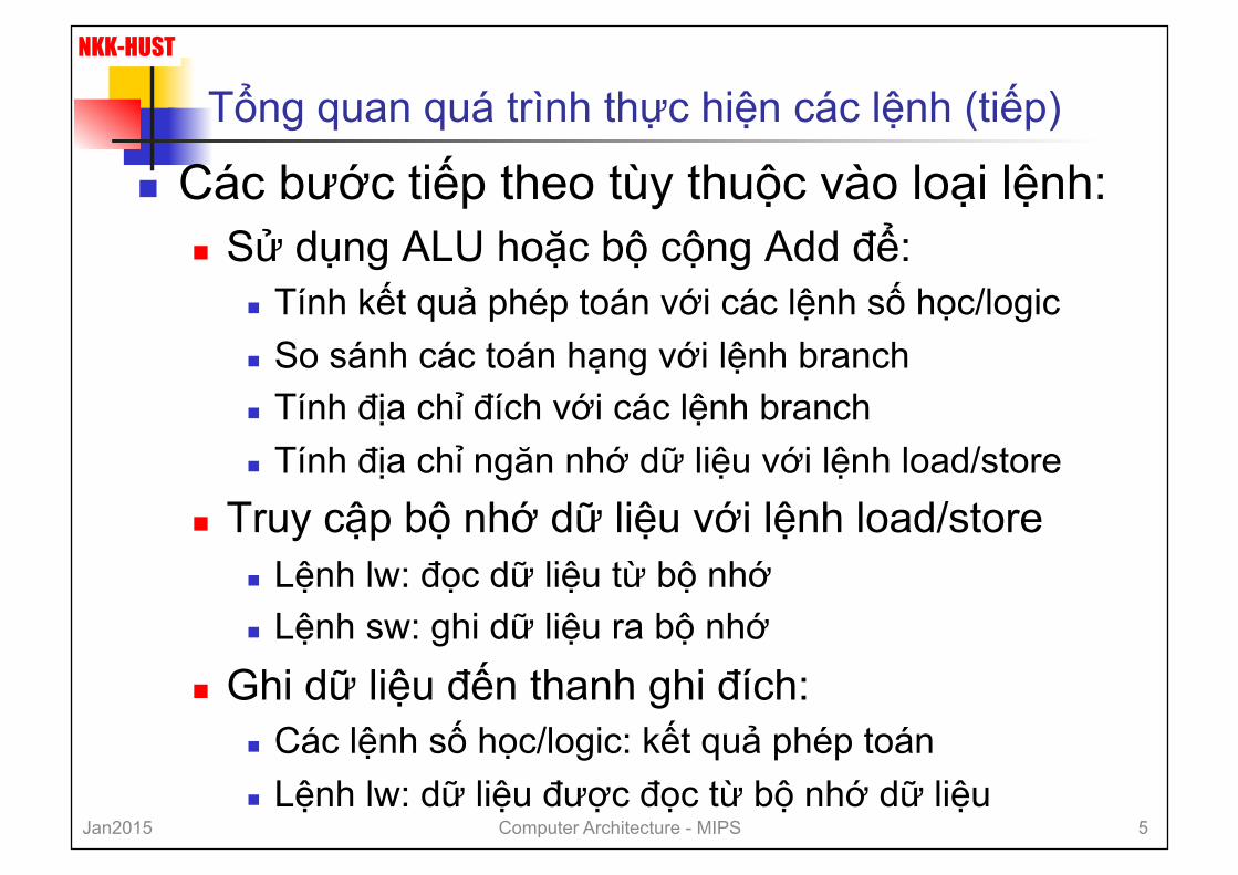
Tổng quan quá trình thực hiện các lệnh (tiếp)
n Các bước tiếp theo tùy thuộc vào loại lệnh: n Sử dụng ALU hoặc bộ cộng Add để:
n Tính kết quả phép toán với các lệnh số học/logic n So sánh các toán hạng với lệnh branch n Tính địa chỉ đích với các lệnh branch n Tính địa chỉ ngăn nhớ dữ liệu với lệnh load/store
n Truy cập bộ nhớ dữ liệu với lệnh load/store n Lệnh lw: đọc dữ liệu từ bộ nhớ n Lệnh sw: ghi dữ liệu ra bộ nhớ
n Ghi dữ liệu đến thanh ghi đích: n Các lệnh số học/logic: kết quả phép toán n Lệnh lw: dữ liệu được đọc từ bộ nhớ dữ liệu
Jan2015 Computer Architecture - MIPS 5

NKK-HUST
Tổng quan quá trình thực hiện các lệnh (tiếp)
n Thay đổi nội dung bộ đếm chương trình PC: n Với các lệnh rẽ nhánh (branch), tùy thuộc vào
kết quả so sánh: n Điều kiện thỏa mãn: PC ß địa chỉ đích (địa chỉ của
lệnh cần rẽ tới) n Điều kiện không thỏa mãn: PC ß PC + 4 (địa chỉ
của lệnh kế tiếp) n Với các lệnh còn lại (không kể các lệnh jump)
n PC ß PC + 4 (địa chỉ của lệnh kế tiếp)
Jan2015 Computer Architecture - MIPS 6

NKK-HUST
Sơ đồ khái quát của bộ xử lý MIPS
Jan2015 Computer Architecture - MIPS 7
NKK-HUST
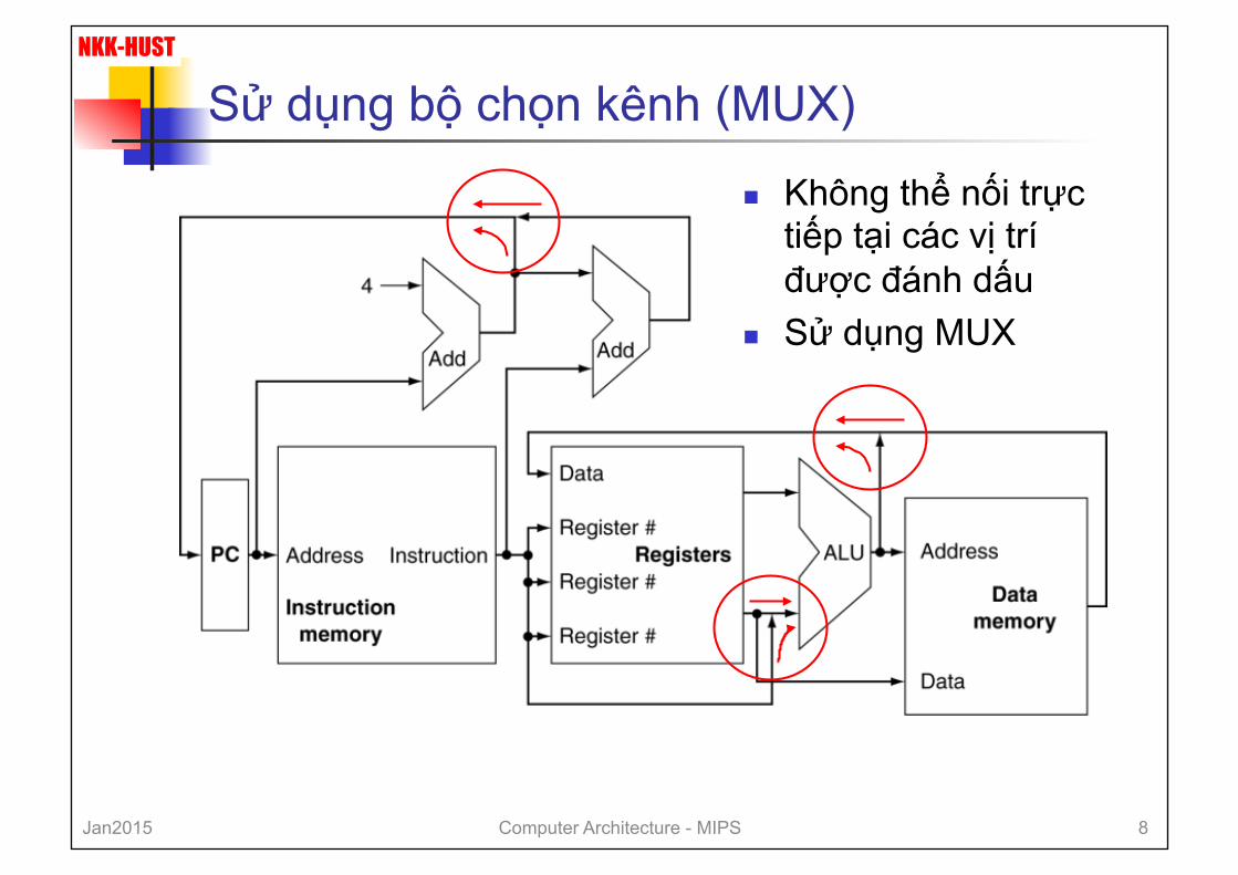
Sử dụng bộ chọn kênh (MUX)
n Không thể nối trực tiếp tại các vị trí được đánh dấu
n Sử dụng MUX
Jan2015 Computer Architecture - MIPS 8

NKK-HUST
Bộ xử lý với các đường điều khiển chính
Jan2015 Computer Architecture - MIPS 9

NKK-HUST
2. Thiết kế khối Datapath
n Datapath: gồm các thành phần để xử lý dữ liệu và địa chỉ n Tập thanh ghi, ALUs, MUX’s, bộ nhớ, …
n Sẽ xây dựng tăng dần khối datapath cho MIPS
Jan2015 Computer Architecture - MIPS 10

NKK-HUST
Các thành phần để thực hiện nhận lệnh
Jan2015 Computer Architecture - MIPS 11
n Bộ đếm chương trình PC: n Thanh ghi 32-bit chứa địa chỉ của lệnh hiện tại n Địa chỉ khởi động = 0xBFC0 0000
n Bộ nhớ lệnh (Instruction memory): n Chứa các lệnh của chương trình n Khi có địa chỉ lệnh từ PC đưa đến thì lệnh được đọc ra
n Bộ cộng (Add): được sử dụng tăng nội dung PC thêm 4 để trỏ tới lệnh kế tiếp
252 Chapter 4 The Processor
which were introduced in Chapter 2. Recall that a typical instance of such an instruction is add $t1,$t2,$t3, which reads $t2 and $t3 and writes $t1.
Th e processor’s 32 general-purpose registers are stored in a structure called a register fi le. A register fi le is a collection of registers in which any register can be read or written by specifying the number of the register in the fi le. Th e register fi le contains the register state of the computer. In addition, we will need an ALU to operate on the values read from the registers.
R-format instructions have three register operands, so we will need to read two data words from the register fi le and write one data word into the register fi le for each instruction. For each data word to be read from the registers, we need an input to the register fi le that specifi es the register number to be read and an output from the register fi le that will carry the value that has been read from the registers. To write a data word, we will need two inputs: one to specify the register number to be written and one to supply the data to be written into the register. Th e register fi le always outputs the contents of whatever register numbers are on the Read register inputs. Writes, however, are controlled by the write control signal, which must be asserted for a write to occur at the clock edge. Figure 4.7a shows the result; we need a total of four inputs (three for register numbers and one for data) and two outputs (both for data). Th e register number inputs are 5 bits wide to specify one of 32 registers (32 = 25), whereas the data input and two data output buses are each 32 bits wide.
Figure 4.7b shows the ALU, which takes two 32-bit inputs and produces a 32-bit result, as well as a 1-bit signal if the result is 0. Th e 4-bit control signal of the ALU is described in detail in Appendix B; we will review the ALU control shortly when we need to know how to set it.
register fi le A state element that consists of a set of registers that can be read and written by supplying a register number to be accessed.
Instructionaddress
Instruction
Instructionmemory
a. Instruction memory
PC
b. Program counter
Add Sum
c. Adder
FIGURE 4.5 Two state elements are needed to store and access instructions, and an adder is needed to compute the next instruction address. Th e state elements are the instruction memory and the program counter. Th e instruction memory need only provide read access because the datapath does not write instructions. Since the instruction memory only reads, we treat it as combinational logic: the output at any time refl ects the contents of the location specifi ed by the address input, and no read control signal is needed. (We will need to write the instruction memory when we load the program; this is not hard to add, and we ignore it for simplicity.) Th e program counter is a 32-bit register that is written at the end of every clock cycle and thus does not need a write control signal. Th e adder is an ALU wired to always add its two 32-bit inputs and place the sum on its output.

NKK-HUST
Thực hiện phần nhận lệnh
32-bit register
Increment by 4 for next instruction
Jan2015 Computer Architecture - MIPS 12

NKK-HUST
Thực hiện lệnh số học/logic kiểu R
n bits 31:26: mã thao tác (opcode) n 000000 với các lệnh kiểu R
n bits 25:21: số hiệu thanh ghi nguồn thứ nhất rs n bits 20:16: số hiệu thanh ghi nguồn thứ hai rt n bits 15:11: số hiệu thanh ghi đích rd n bits 10:6: số bit được dịch với các lệnh dịch bit
n 00000 với các lệnh khác
n bits 5:0: mã hàm để xác định phép toán (function code)
Jan2015 Computer Architecture - MIPS 13
op rs rt rd shamt funct
31:26 5:0 25:21 20:16 15:11 10:6

NKK-HUST
Các thành phần thực hiện lệnh kiểu R
Jan2015 Computer Architecture - MIPS 14
310 Chapter 4 The Processor
In addition, we will need a unit to sign-extend the 16-bit offset field in the instruction to a 32-bit signed value, and a data memory unit to read from or write to. The data memory must be written on store instructions; hence, data memory has read and write control signals, an address input, and an input for the data to be written into memory. Figure 4.8 shows these two elements.
The beq instruction has three operands, two registers that are compared for equality, and a 16-bit offset used to compute the branch target address relative to the branch instruction address. Its form is beq $t1,$t2,offset. To implement this instruction, we must compute the branch target address by adding the sign-extended offset field of the instruction to the PC. There are two details in the definition of branch instructions (see Chapter 2) to which we must pay attention:
■ The instruction set architecture specifies that the base for the branch address calculation is the address of the instruction following the branch. Since we compute PC + 4 (the address of the next instruction) in the instruction fetch datapath, it is easy to use this value as the base for computing the branch target address.
sign-extend To increase the size of a data item by replicating the high-order sign bit of the original data item in the high-order bits of the larger, destina tion data item.
branch target address The address specified in a branch, which becomes the new program counter (PC) if the branch is taken. In the MIPS architecture the branch target is given by the sum of the offset field of the instruction and the address of the instruction following the branch.
FIGURE 4.7 The two elements needed to implement R-format ALU operations are the register file and the ALU. The register file contains all the registers and has two read ports and one write port. The design of multiported register files is discussed in Section C.8 of Appendix C. The register file always outputs the contents of the registers corresponding to the Read register inputs on the outputs; no other control inputs are needed. In contrast, a register write must be explicitly indicated by asserting the write control signal. Remember that writes are edge-t riggered, so that all the write inputs (i.e., the value to be written, the register number, and the write control signal) must be valid at the clock edge. Since writes to the register file are edge-t riggered, our design can legally read and write the same register within a clock cycle: the read will get the value written in an earlier clock cycle, while the value written will be available to a read in a subsequent clock cycle. The inputs carrying the register number to the register file are all 5 bits wide, whereas the lines carrying data values are 32 bits wide. The operation to be performed by the ALU is controlled with the ALU operation signal, which will be 4 bits wide, using the ALU designed in Appendix C. We will use the Zero detection output of the ALU shortly to implement branches. The overflow output will not be needed until Section 4.9, when we discuss exceptions; we omit it until then.
Readregister 1
Registers ALUData
Data
ZeroALU
result
RegWrite
a. Registers b. ALU
5
5
5
Registernumbers
Readdata 1
Readdata 2
ALU operation4
Readregister 2WriteregisterWriteData
n Tập thanh ghi (Registers): có 32 thanh ghi 32-bit, mỗi thanh ghi được xác định bởi số hiệu 5-bit n Read register 1, Read register 2: các đầu vào để chọn các thanh ghi
cần đọc n Write register: đầu vào để chọn thanh ghi cần ghi n Read data 1, Read data 2: hai đầu ra dữ liệu đọc từ thanh ghi (32-bit) n Write Data: đầu vào dữ liệu ghi vào thanh ghi (32-bit) n RegWrite: tín hiệu điều khiển ghi dữ liệu vào thanh ghi
n ALU để thực hiện các phép toán số học/logic

NKK-HUST
Mô tả thực hiện lệnh số học/logic kiểu R
Jan2015 Computer Architecture - MIPS 15
n Hai số hiệu thanh ghi rs và rt đưa đến hai đầu vào Read register 1, Read register 2 để chọn hai thanh ghi nguồn
n Số hiệu thanh ghi rd đưa đến đầu vào Write register để chọn thanh ghi đích
n Hai dữ liệu từ hai thanh ghi nguồn được đọc ra 2 đầu ra Read data 1 và Read data 2 , rồi đưa đến đầu vào của ALU
n ALU operation (4-bit): tín hiệu điều khiển chọn phép toán ở ALU
n ALU thực hiện phép toán tương ứng, kết quả phép toán ở đầu ra ALU result được đưa về đầu vào Write Data của tập thanh ghi để ghi vào thanh ghi đích
n RegWrite: tín hiệu điều khiển ghi dữ liệu vào thanh ghi đích

NKK-HUST
Thực hiện các lệnh lw/sw
n bits 31:26 là mã thao tác n 100011 (35) với lệnh lw n 101011 (43) với lệnh sw
n bits 25:21: số hiệu thanh ghi cơ sở rs n bits 20:16: số hiệu thanh ghi rt
n thanh ghi đích với lệnh lw n thanh ghi nguồn với lệnh sw
n bits 15:0: hằng số imm có giá trị trong dải [-215 , +215 – 1] n Địa chỉ từ nhớ dữ liệu = nội dung thanh ghi rs + imm n lw rt, imm(rs) # (rt) = mem[(rs)+SignExtImm]
n sw rt, imm(rs) # mem[(rs)+SignExtImm] = (rt) Jan2015 Computer Architecture - MIPS 16
op rs rt imm
31:26 25:21 20:16 15:0

NKK-HUST
Các thành phần thực hiện các lệnh lw/sw
Jan2015 Computer Architecture - MIPS 17
■ The architecture also states that the offset field is shifted left 2 bits so that it is a word offset; this shift increases the effective range of the offset field by a factor of 4.
To deal with the latter complication, we will need to shift the offset field by 2. As well as computing the branch target address, we must also determine whether
the next instruction is the instruction that follows sequentially or the instruction at the branch target address. When the condition is true (i.e., the operands are equal), the branch target address becomes the new PC, and we say that the branch is taken. If the operands are not equal, the incremented PC should replace the current PC (just as for any other normal instruction); in this case, we say that the branch is not taken.
Thus, the branch datapath must do two operations: compute the branch target address and compare the register contents. (Branches also affect the instruction fetch portion of the datapath, as we will deal with shortly.) Figure 4.9 shows the structure of the datapath segment that handles branches. To compute the branch target address, the branch datapath includes a sign extension unit, from Figure 4.8 and an adder. To perform the compare, we need to use the register file shown in Figure 4.7a to supply the two register operands (although we will not need to write into the register file). In addition, the comparison can be done using the ALU we designed in Appendix C. Since that ALU provides an output signal that indicates whether the result was 0, we can send the two register operands to the ALU with the
branch taken A branch where the branch condition is satisfied and the program counter (PC) becomes the branch target. All unconditional branches are taken branches.
branch not taken or (untaken branch) A branch where the branch condition is false and the program counter (PC) becomes the address of the instruction that sequentially follows the branch.
FIGURE 4.8 The two units needed to implement loads and stores, in addition to the register file and ALU of Figure 4.7, are the data memory unit and the sign extension unit. The memory unit is a state element with inputs for the address and the write data, and a single output for the read result. There are separate read and write controls, although only one of these may be asserted on any given clock. The memory unit needs a read signal, since, unlike the register file, reading the value of an invalid address can cause problems, as we will see in Chapter 5. The sign extension unit has a 16-bit input that is sign-extended into a 32-bit result appearing on the output (see Chapter 2). We assume the data memory is edge-triggered for writes. Standard memory chips actually have a write enable signal that is used for writes. Although the write enable is not edge-triggered, our edge-triggered design could easily be adapted to work with real memory chips. See Section C.8 of Appendix C for further discussion of how real memory chips work.
Address Readdata
Datamemory
a. Data memory unit
Writedata
MemRead
MemWrite
b. Sign extension unit
Sign-extend
16 32
4.3 Building a Datapath 311
310 Chapter 4 The Processor
In addition, we will need a unit to sign-extend the 16-bit offset field in the instruction to a 32-bit signed value, and a data memory unit to read from or write to. The data memory must be written on store instructions; hence, data memory has read and write control signals, an address input, and an input for the data to be written into memory. Figure 4.8 shows these two elements.
The beq instruction has three operands, two registers that are compared for equality, and a 16-bit offset used to compute the branch target address relative to the branch instruction address. Its form is beq $t1,$t2,offset. To implement this instruction, we must compute the branch target address by adding the sign-extended offset field of the instruction to the PC. There are two details in the definition of branch instructions (see Chapter 2) to which we must pay attention:
■ The instruction set architecture specifies that the base for the branch address calculation is the address of the instruction following the branch. Since we compute PC + 4 (the address of the next instruction) in the instruction fetch datapath, it is easy to use this value as the base for computing the branch target address.
sign-extend To increase the size of a data item by replicating the high-order sign bit of the original data item in the high-order bits of the larger, destina tion data item.
branch target address The address specified in a branch, which becomes the new program counter (PC) if the branch is taken. In the MIPS architecture the branch target is given by the sum of the offset field of the instruction and the address of the instruction following the branch.
FIGURE 4.7 The two elements needed to implement R-format ALU operations are the register file and the ALU. The register file contains all the registers and has two read ports and one write port. The design of multiported register files is discussed in Section C.8 of Appendix C. The register file always outputs the contents of the registers corresponding to the Read register inputs on the outputs; no other control inputs are needed. In contrast, a register write must be explicitly indicated by asserting the write control signal. Remember that writes are edge-t riggered, so that all the write inputs (i.e., the value to be written, the register number, and the write control signal) must be valid at the clock edge. Since writes to the register file are edge-t riggered, our design can legally read and write the same register within a clock cycle: the read will get the value written in an earlier clock cycle, while the value written will be available to a read in a subsequent clock cycle. The inputs carrying the register number to the register file are all 5 bits wide, whereas the lines carrying data values are 32 bits wide. The operation to be performed by the ALU is controlled with the ALU operation signal, which will be 4 bits wide, using the ALU designed in Appendix C. We will use the Zero detection output of the ALU shortly to implement branches. The overflow output will not be needed until Section 4.9, when we discuss exceptions; we omit it until then.
Readregister 1
Registers ALUData
Data
ZeroALU
result
RegWrite
a. Registers b. ALU
5
5
5
Registernumbers
Readdata 1
Readdata 2
ALU operation4
Readregister 2WriteregisterWriteData
Bộ số học/logic Tập thanh ghi
Bộ mở rộng số có dấu từ 16-bit à 32-bit
Bộ nhớ dữ liệu

NKK-HUST
Thực hiện lệnh lw n Số hiệu thanh ghi rs đưa đến đầu vào Read register 1 để
chọn thanh ghi cơ sở rs, nội dung rs được đưa ra đầu ra Read Data 1, rồi chuyển đến ALU
n Hằng số imm 16-bit đưa đến bộ Sign-extend để mở rộng thành 32-bit, rồi chuyển đến ALU
n ALU cộng hai giá trị trên đưa ra ALU result chính là địa chỉ của dữ liệu cần đọc từ bộ nhớ dữ liệu; địa chỉ này được đưa đến đầu vào Address của bộ nhớ dữ liệu
n Số hiệu thanh ghi rt đưa đến đầu vào Write Register để chọn thanh ghi đích
n Dữ liệu 32-bit ở bộ nhớ dữ liệu, tại vị trí địa chỉ đã được tính, được đọc ra ở đầu ra Read data của bộ nhớ dữ liệu nhờ tín hiệu điều khiển MemRead, rồi đưa về đầu vào Write Data của tập thanh ghi để ghi vào thanh ghi đích rt
Jan2015 Computer Architecture - MIPS 18

NKK-HUST
Thực hiện lệnh sw n Số hiệu thanh ghi rs đưa đến đầu vào Read register 1 để
chọn thanh ghi cơ sở rs, nội dung rs được đưa ra đầu ra Read Data 1, rồi chuyển đến ALU
n Hằng số imm 16-bit đưa đến bộ Sign-extend để mở rộng thành 32-bit, rồi chuyển đến ALU
n ALU cộng hai giá trị trên đưa ra ALU result chính là địa chỉ của vị trí ở bộ nhớ dữ liệu; địa chỉ này được đưa đến đầu vào Address của bộ nhớ dữ liệu
n Số hiệu thanh ghi rt đưa đến đầu vào Read register 2 để chọn thanh ghi dữ liệu nguồn rt, nội dung rt được đưa ra đầu ra Read data 2
n Dữ liệu 32-bit này sẽ được đưa đến đầu vào Write data của bộ nhớ dữ liệu và được ghi vào vị trí nhớ có địa chỉ đã được tính, nhờ tín hiệu điều khiển MemWrite
Jan2015 Computer Architecture - MIPS 19

NKK-HUST
Thực hiện lệnh Branch (beq, bne)
Jan2015 Computer Architecture - MIPS 20
4 or 5 rs rt imm
31:26 25:21 20:16 15:0
n bits 31:26 mã thao tác n 000100 (4) với lệnh beq n 000101 (5) với lệnh bne
n bits 25:21 số hiệu thanh ghi nguồn rs n bits 20:16 số hiệu thanh ghi nguồn rt n bits 15:0 hằng số imm có giá trị trong dải [-215 , +215 – 1] n So sánh nội dung hai thanh ghi rs và rt:
n Nếu điều kiện đúng: rẽ nhánh đến nhãn đích n PC ß (PC +4) + hằng số x 4
n Nếu điều kiện sai: chuyển sang thực hiện lệnh kế tiếp n PC ß PC + 4
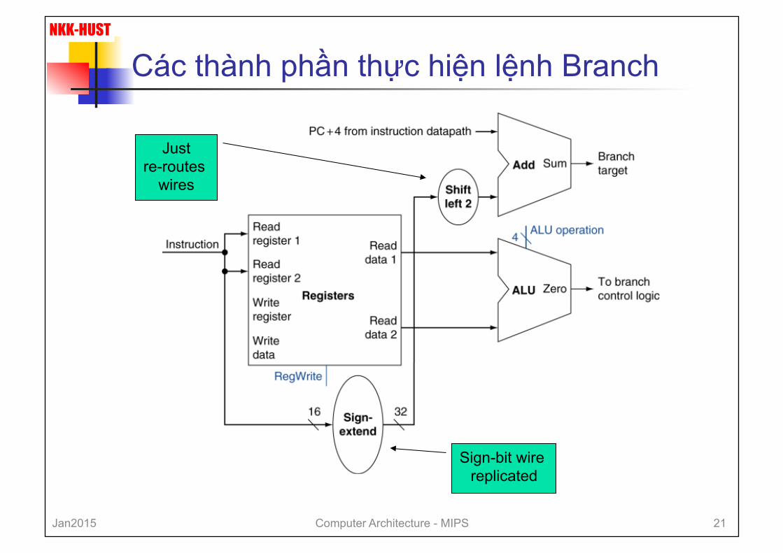
NKK-HUST
Các thành phần thực hiện lệnh Branch
Just re-routes
wires
Sign-bit wire replicated
Jan2015 Computer Architecture - MIPS 21

NKK-HUST
Thực hiện lệnh Branch (beq, bne)
n Nhờ các số hiệu thanh ghi rs và rt, hai toán hạng nguồn được đọc ra đưa đến ALU
n ALU trừ hai toán hạng và thiết lập giá trị ở đầu ra “Zero” n Hiệu = 0 à đầu ra Zero = 1 n Hiệu <> 0 à đầu ra Zero = 0 n Đầu ra Zero này được đưa đến mạch logic điều khiển rẽ nhánh
n Bộ cộng Add tính địa chỉ đích rẽ nhánh n Hằng số imm 16-bit được mở rộng theo kiểu có dấu thành 32-bit,
rồi dịch trái 2 bit n Cộng với PC (PC đã được tăng 4) à Địa chỉ đích = (PC+4) + (hằng số đã mở rộng 32-bit, dịch trái 2 bit)
n Điều kiện đúng: PC ß địa chỉ đích rẽ nhánh (rẽ nhánh xảy ra)
n Điều kiện sai: PC ß PC+4 (chuyển sang lệnh kế tiếp)
Jan2015 Computer Architecture - MIPS 22

NKK-HUST
Hợp các thành phần cho các lệnh
n Datapath cho các lệnh thực hiện trong 1 chu kỳ n Mỗi phần tử của datapath chỉ có thể làm
một chức năng trong mỗi chu kỳ n Do đó, cần tách rời bộ nhớ lệnh và bộ
nhớ dữ liệu n Sử dụng các bộ chọn kênh để chọn dữ
liệu nguồn cho các lệnh khác nhau
Jan2015 Computer Architecture - MIPS 23

NKK-HUST
Datapath cho các lệnh R-Type/Load/Store
Jan2015 Computer Architecture - MIPS 24
• ALUSrc: tín hiệu điều khiển chọn toán hạng đưa đến ALU: • Lệnh kiểu R: toán hạng từ thanh ghi nguồn thứ hai • Lệnh lw/sw: Hằng số imm 16-bit được mở rộng thành 32-bit (tính địa chỉ)
• MemtoReg: tín hiệu điều khiển chọn dữ liệu đưa về thanh ghi đích: • Lệnh kiểu R: lấy kết quả từ ALU result • Lệnh lw: dữ liệu đọc (Read data) từ bộ nhớ dữ liệu

NKK-HUST
Datapath đơn giản cho các lệnh R/lw/sw/branch
Jan2015 Computer Architecture - MIPS 25
• PCSrc: tín hiệu điều khiển chọn giá trị cập nhật PC • Không rẽ nhánh: PC ß PC+4 • Rẽ nhánh: PC ß (PC+4) + (hằng số imm đã mở rộng thành 32-bit << 2)

NKK-HUST
3. Thiết kế Control Unit
n Đơn vị điều khiển có hai phần: n Bộ điều khiển ALU n Bộ điều khiển chính
Jan2015 Computer Architecture - MIPS 26

NKK-HUST
Thiết kế bộ điều khiển ALU
n ALU được sử dụng để: n Load/Store: F = add (xác định địa chỉ bộ nhớ dữ liệu) n Branch: F = subtract (so sánh) n Các lệnh số học/logic : F phụ thuộc vào funct code
ALU control lines Function
0000 AND
0001 OR
0010 add
0110 subtract
0111 set-on-less-than
1100 NOR
Jan2015 Computer Architecture - MIPS 27

NKK-HUST
Tín hiệu điều khiển ALU n Bộ điều khiển ALU sử dụng mạch logic tổ hợp:
n Đầu vào: 2-bit ALUOp được tạo ra từ opcode của lệnh và 6-bit của function code
n Đầu ra: các tín hiệu điều khiển ALU (ALU control) gồm 4 bit
Opcode ALUOp Operation funct ALU function ALU control lw 00 load word XXXXXX add 0010
sw 00 store word XXXXXX add 0010 beq 01 branch equal XXXXXX subtract 0110 R-type 10 add 100000 add 0010
subtract 100010 subtract 0110 AND 100100 AND 0000 OR 100101 OR 0001
set-on-less-than 101010 set-on-less-than 0111
Jan2015 Computer Architecture - MIPS 28

NKK-HUST
Thiết kế bộ điều khiển chính
n Các tín hiệu điều khiển được tạo ra từ lệnh
0 rs rt rd shamt funct
31:26 5:0 25:21 20:16 15:11 10:6
35 or 43 rs rt imm
31:26 25:21 20:16 15:0
4 rs rt imm
31:26 25:21 20:16 15:0
R-type
lw/sw
beq
opcode always read
read, except for load
write for R-type
and load
sign-extend and add
Jan2015 Computer Architecture - MIPS 29

NKK-HUST
Datapath và Control Unit
Jan2015 Computer Architecture - MIPS 30

NKK-HUST
Các tín hiệu điều khiển
Jan2015 Computer Architecture - MIPS 31
Tên tín hiệu Hiệu ứng khi tín hiệu = 0 Hiệu ứng khi tín hiệu = 1 RegDst Số hiệu thanh ghi đích là các
bit 20:16 (rt) Số hiệu thanh ghi đích là các bit 15:11 (rd)
Branch Không có lệnh rẽ nhánh beq Có lệnh rẽ nhánh beq (Branch =1) & (Zero=1): rẽ nhánh xảy ra (Branch =1) & (Zero=0): rẽ nhánh không xảy ra
RegWrite Không làm gì cả Ghi dữ liệu trên đầu vào Write Data ở tập thanh ghi đến thanh ghi đích
ALUSrc Toán hạng thứ hai của ALU lấy từ thanh ghi nguồn thứ hai (Read data 2)
Toán hạng thứ hai của ALU là giá trị 16 bit thấp của lệnh (bits 15:0) được mở rộng có dấu thành 32-bit
PCSrc PC ß PC+4 PC ß địa chỉ đích

NKK-HUST
Các tín hiệu điều khiển (tiếp)
Jan2015 Computer Architecture - MIPS 32
Tên tín hiệu Hiệu ứng khi tín hiệu = 0 Hiệu ứng khi tín hiệu = 1 MemRead Không làm gì cả
Nội dung ngăn nhớ dữ liệu, được xác định bởi địa chỉ do ALU tính, được đưa ra đầu ra Read data của bộ nhớ dữ liệu
MemWrite Không làm gì cả
Dữ liệu trên đầu vào Write Data của bộ nhớ dữ liệu được ghi vào ngăn nhớ có địa chỉ do ALU tính
MemtoReg Giá trị được đưa đến đầu vào Write data của tập thanh ghi là từ ALU result
Giá trị được đưa đến đầu vào Write data của tập thanh ghi là từ bộ nhớ dữ liệu

NKK-HUST
Thực hiện lệnh số học/logic kiểu R
Jan2015 Computer Architecture - MIPS 33

NKK-HUST
Thực hiện lệnh Load
Jan2015 Computer Architecture - MIPS 34

NKK-HUST
Thực hiện lệnh beq
Jan2015 Computer Architecture - MIPS 35

NKK-HUST
Thực hiện lệnh Jump
n Bits 31:26 là mã thao tác = 000010 n Bits 25:0: phần địa chỉ n PC nhận giá trị sau:
n Địa chỉ đích = PC31…28 : (address << 2) n 4 bit bên trái là của PC cũ n 26-bit của lệnh jump (bits 25:0) n 2 bit cuối là 00
n Cần thêm tín hiệu điều khiển được giải mã từ opcode
2 address
31:26 25:0
Jan2015 Computer Architecture - MIPS 36
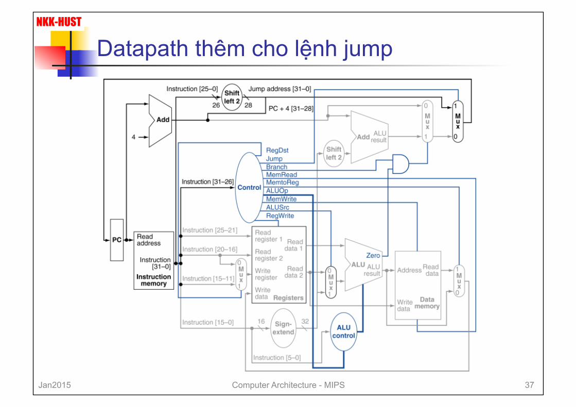
NKK-HUST
Datapath thêm cho lệnh jump
Jan2015 Computer Architecture - MIPS 37

NKK-HUST
Thiết kế đơn chu kỳ (single-cycle)
n Chu kỳ xung nhịp có độ dài bằng nhau với tất cả các lệnh à chu kỳ xung nhịp được xác định bởi thời gian thực thi lệnh lâu nhất
n Ví dụ: Lệnh load sử dụng 5 đơn vị chức năng: Bộ nhớ lệnh → tập thanh ghi → ALU → bộ nhớ dữ liệu → tập thanh ghi
n Thời gian thực hiện chương trình tăng à hiệu năng giảm
n Chúng ta sẽ tăng hiệu năng bằng kỹ thuật đường ống lệnh (pipelining)
Jan2015 Computer Architecture - MIPS 38

NKK-HUST
4. Đường ống lệnh ở MIPS
5 công đoạn: 1. IF: Instruction fetch from memory – Nhận lệnh từ
bộ nhớ 2. ID: Instruction decode & register read – Giải mã
lệnh và đọc thanh ghi 3. EX: Execute operation or calculate address – Thực
hiện thao tác hoặc tính toán địa chỉ 4. MEM: Access memory operand – Truy nhập toán
hạng bộ nhớ 5. WB: Write result back to register – Ghi kết quả trả
về thanh ghi
Jan2015 Computer Architecture - MIPS 39

NKK-HUST
Hiệu năng của đường ống
n Giả thiết thời gian cho các công đoạn: n 100ps với đọc hoặc ghi thanh ghi n 200ps cho các công đoạn khác
n Thời gian của datapath đơn chu kỳ với một số lệnh:
Instr Instr fetch Register read
ALU op Memory access
Register write
Total time
lw 200ps 100 ps 200ps 200ps 100 ps 800ps
sw 200ps 100 ps 200ps 200ps 700ps
R-format 200ps 100 ps 200ps 100 ps 600ps
beq 200ps 100 ps 200ps 500ps
Jan2015 Computer Architecture - MIPS 40

NKK-HUST
Hiệu năng của đường ống
Single-cycle (Tc= 800ps)
Pipelined (Tc= 200ps)
Jan2015 Computer Architecture - MIPS 41

NKK-HUST
Độ tăng tốc của đường ống
n Nếu tất cả các công đoạn có thời gian thực hiện như nhau và số lệnh của chương trình là lớn:
Thời gian thực hiện pipeline = Thời gian thực hiện tuần tự Số công đoạn
Jan2015 Computer Architecture - MIPS 42

NKK-HUST
Thiết kế đường ống lệnh n Kiến trúc tập lệnh MIPS được thiết kế phù
hợp với kỹ thuật đường ống n Tất cả các lệnh là 32-bits
n Dễ dàng để nhận và giải mã lệnh trong một chu kỳ n Intel x86: lệnh từ 1 đến 17 bytes
n Có ít dạng lệnh và thông dụng n Có thể giải mã và đọc thanh ghi trong một bước
n Địa chỉ hóa cho các lệnh load/store n Có thể tính địa chỉ trong công đoạn thứ 3, truy cập
bộ nhớ công đoạn thứ 4 n Toán hạng bộ nhớ nằm thẳng hàng trên các
băng nhớ n Truy cập bộ nhớ chỉ mất một chu kỳ
Jan2015 Computer Architecture - MIPS 43

NKK-HUST
Các mối trở ngại (Hazard) của đường ống lệnh
n Hazard: Tình huống ngăn cản bắt đầu của lệnh tiếp theo ở chu kỳ tiếp theo n Hazard cấu trúc: do tài nguyên được yêu
cầu đang bận n Hazard dữ liệu: cần phải đợi để lệnh trước
hoàn thành việc đọc/ghi dữ liệu n Hazard điều khiển: do rẽ nhánh gây ra
Jan2015 Computer Architecture - MIPS 44

NKK-HUST
Hazard cấu trúc
n Xung đột khi sử dụng tài nguyên n Trong đường ống của MIPS với một bộ
nhớ dùng chung n Lệnh Load/store yêu cầu truy cập dữ liệu n Nhận lệnh cần trì hoãn cho chu kỳ đó
n Bởi vậy, datapath kiểu đường ống yêu cầu bộ nhớ lệnh và bộ nhớ dữ liệu tách rời (hoặc cache lệnh/cache dữ liệu tách rời)
Jan2015 Computer Architecture - MIPS 45

NKK-HUST
Hazard dữ liệu
n Lệnh phụ thuộc vào việc hoàn thành truy cập dữ liệu của lệnh trước đó add $s0, $t0, $t1 sub $t2, $s0, $t3
Jan2015 Computer Architecture - MIPS 46

NKK-HUST
Forwarding (gửi vượt trước)
n Sử dụng kết quả ngay sau khi nó được tính n Không đợi đến khi kết quả được lưu đến thanh
ghi n Yêu cầu có đường kết nối thêm trong datapath
Jan2015 Computer Architecture - MIPS 47

NKK-HUST
Hazard dữ liệu với lệnh load
n Không phải luôn luôn có thể tránh trì hoãn bằng cách forwarding n Nếu giá trị chưa được tính khi cần thiết n Không thể chuyển ngược thời gian n Cần chèn bước trì hoãn (stall hay bubble)
Jan2015 Computer Architecture - MIPS 48

NKK-HUST
Lập lịch mã để tránh trì hoãn n Thay đổi trình tự mã để tránh sử dụng kết
quả load ở lệnh tiếp theo n Mã C:
a = b + e; c = b + f;
lw $t1, 0($t0)
lw $t2, 4($t0)
add $t3, $t1, $t2
sw $t3, 12($t0)
lw $t4, 8($t0)
add $t5, $t1, $t4
sw $t5, 16($t0)
stall
stall
lw $t1, 0($t0)
lw $t2, 4($t0)
lw $t4, 8($t0)
add $t3, $t1, $t2
sw $t3, 12($t0)
add $t5, $t1, $t4
sw $t5, 16($t0)
11 cycles 13 cycles Jan2015 Computer Architecture - MIPS 49

NKK-HUST
Hazard điều khiển
n Rẽ nhánh xác định luồng điều khiển n Nhận lệnh tiếp theo phụ thuộc vào kết quả
rẽ nhánh n Đường ống không thể luôn nhận đúng lệnh
n Vẫn đang làm ở công đoạn giải mã lệnh (ID) của lệnh rẽ nhánh
n Với đường ống của MIPS n Cần so sánh thanh ghi và tính địa chỉ đích
sớm trong đường ống n Thêm phần cứng để thực hiện việc đó
trong công đoạn ID
Jan2015 Computer Architecture - MIPS 50

NKK-HUST
Trì hoãn khi rẽ nhánh
n Đợi cho đến khi kết quả rẽ nhánh đã được xác định trước khi nhận lệnh tiếp theo
Jan2015 Computer Architecture - MIPS 51

NKK-HUST
Dự đoán rẽ nhánh
n Những đường ống dài hơn không thể sớm xác định dễ dàng kết quả rẽ nhánh n Cách trì hoãn không đáp ứng được
n Dự đoán kết quả rẽ nhánh n Chỉ trì hoãn khi dự đoán là sai
n Với MIPS n Có thể dự đoán rẽ nhánh không xẩy ra n Nhận lệnh ngay sau lệnh rẽ nhánh (không
làm trễ)
Jan2015 Computer Architecture - MIPS 52

NKK-HUST
MIPS với dự đoán rẽ nhánh không xẩy ra
Prediction correct
Prediction incorrect
Jan2015 Computer Architecture - MIPS 53

NKK-HUST
Đặc điểm của đường ống
n Kỹ thuật đường ống cải thiện hiệu năng bằng cách tăng số lệnh thực hiện n Thực hiện nhiều lệnh đồng thời n Mỗi lệnh có cùng thời gian thực hiện
n Các dạng hazard: n Cấu trúc, dữ liệu, điều khiển
n Thiết kế tập lệnh ảnh hưởng đến độ phức tạp của việc thực hiện đường ống
Jan2015 Computer Architecture - MIPS 54

NKK-HUST
MIPS Datapath được ống hóa theo đơn chu kỳ
WB
MEM
Jan2015 Computer Architecture - MIPS 55

NKK-HUST
Nhận xét
Jan2015 Computer Architecture - MIPS 56
n Các lệnh và các dữ liệu được chuyển từ trái sang phải qua 5 công đoạn.
n Có hai ngoại lệ từ phải sang trái: n Công đoạn write-back đặt kết quả về thanh
ghi ở giữa datapath à dẫn đến data hazard n Chọn giá trị tiếp theo của PC là PC+4 hay địa
chỉ đích rẽ nhánh từ công đoạn MEM à dẫn đến control hazard

NKK-HUST
Các thanh ghi đường ống
n Cần các thanh ghi đặt giữa các công đoạn n Để giữ thông tin được tạo ra bởi chu kỳ trước
Jan2015 Computer Architecture - MIPS 57

NKK-HUST
Hoạt động của đường ống
n Dòng lệnh được đưa qua datapath đường ống theo từng chu kỳ.
n Có hai cách thực hiện: n Đơn chu kỳ (Single-clock-cycle) n Đa chu kỳ (Multi-clock-cycle)
n Xem xét đường ống đơn chu kỳ với load & store
Jan2015 Computer Architecture - MIPS 58

NKK-HUST
IF cho lệnh Load, Store
Jan2015 Computer Architecture - MIPS 59

NKK-HUST
ID cho lệnh Load, Store
Jan2015 Computer Architecture - MIPS 60

NKK-HUST
EX cho lệnh Load
Jan2015 Computer Architecture - MIPS 61

NKK-HUST
MEM cho lệnh Load
Jan2015 Computer Architecture - MIPS 62

NKK-HUST
WB cho lệnh Load
Wrong register number
Jan2015 Computer Architecture - MIPS 63

NKK-HUST
Datapath được hiệu chỉnh cho lệnh Load
Jan2015 Computer Architecture - MIPS 64

NKK-HUST
EX cho lệnh Store
Jan2015 Computer Architecture - MIPS 65

NKK-HUST
MEM cho lệnh Store
Jan2015 Computer Architecture - MIPS 66

NKK-HUST
WB cho lệnh Store
Jan2015 Computer Architecture - MIPS 67

NKK-HUST
Giản đồ đường ống đa chu kỳ
n Dạng tài nguyên được sử dụng
Jan2015 Computer Architecture - MIPS 68

NKK-HUST
Giản đồ đường ống đa chu kỳ
n Dạng truyền thống
Jan2015 Computer Architecture - MIPS 69

NKK-HUST
Giản đồ đường ống đơn chu kỳ
n Công đoạn của đường ống trong chu kỳ đã cho
Jan2015 Computer Architecture - MIPS 70

NKK-HUST
Điều khiển đường ống (dạng đơn giản)
Jan2015 Computer Architecture - MIPS 71

NKK-HUST
Điều khiển đường ống
n Các tín hiệu điều khiển được tạo ra từ lệnh n Như thực hiện đơn chu kỳ
Jan2015 Computer Architecture - MIPS 72

NKK-HUST
Điều khiển đường ống
Jan2015 Computer Architecture - MIPS 73

NKK-HUST
Hết
Jan2015 Computer Architecture - MIPS 74