Ng, Andrew Eng Jwee (1999) Switched-current filtering systems
216
Glasgow Theses Service http://theses.gla.ac.uk/ [email protected] Ng, Andrew Eng Jwee (1999) Switched-current filtering systems: design, synthesis and software development. PhD thesis. http://theses.gla.ac.uk/5040/ Copyright and moral rights for this thesis are retained by the author A copy can be downloaded for personal non-commercial research or study, without prior permission or charge This thesis cannot be reproduced or quoted extensively from without first obtaining permission in writing from the Author The content must not be changed in any way or sold commercially in any format or medium without the formal permission of the Author When referring to this work, full bibliographic details including the author, title, awarding institution and date of the thesis must be given
-
Upload
khangminh22 -
Category
Documents
-
view
4 -
download
0
Transcript of Ng, Andrew Eng Jwee (1999) Switched-current filtering systems

Glasgow Theses Service http://theses.gla.ac.uk/
Ng, Andrew Eng Jwee (1999) Switched-current filtering systems: design, synthesis and software development. PhD thesis. http://theses.gla.ac.uk/5040/ Copyright and moral rights for this thesis are retained by the author A copy can be downloaded for personal non-commercial research or study, without prior permission or charge This thesis cannot be reproduced or quoted extensively from without first obtaining permission in writing from the Author The content must not be changed in any way or sold commercially in any format or medium without the formal permission of the Author When referring to this work, full bibliographic details including the author, title, awarding institution and date of the thesis must be given

Switched-Current Filtering Systems:
Design, Synthesis
and
Software Development
A Thesis submitted to the
Faculty of Engineering
of the University of Glasgow
for the degree of
Doctor of Philosophy
by
ANDREW NG ENG JWEE
September 1999
© A.E.J. Ng 1999

SUMMARY
The scope of this thesis covers aspects of the design and synthesis of different
switched-current filtering systems and their implementation into the filter and
equaliser compiler XFIL T. Previous work on matrix -based design of SI filters was
focused mainly on general Left and Right decomposition structures of modest order.
This has been extended to include other decompositions, namely the LU-UL and UL-
LU decompositions, which have shown potential for wideband applications. The
design of very high order filters constraints the choice of filter structure to that of a
doubly-terminated ladder because of its inherent low passband sensitivity. Other
factors that determine the feasibility of a design include the component value spread
and total circuit size or area. A prototype manipulation scheme that is applicable to
matrix-derived bilinear-LDI type filters has been exploited to design very high order
SI filters with effective reductions in spreads and area. For the designed example of a
21st order lowpass filter, a remarkable reduction in spread and area of 99.94% and
99.83% respectively was achieved. Modifications to the general Left and Right
decomposition structures also yielded simple input circuitry and avoided a dynamic-
range scaling problem inherent to Right decomposition structures.
Allpass filters are commonly employed in many applications to perform group delay
equalisation in the passband. They are non-minimum phase by definition and are
characterised by poles and zeros in mirror-image symmetry. SI allpass filters of both
cascade biquad and bilinear-LDI ladder types have been in existence. These were
implemented using Euler based integrators. Cascade biquads are known to have
highly sensitive amplitude responses and Euler integrators suffer from excess phase.
The equalisers that are proposed here are based on bilinear integrators instead of Euler
ones. Derivation of these equalisers can proceed from either the s-domain, or directly
from the z-domain, where a prototype is synthesised using the respective continued-
fractions expansions, and simulated using.~t~dard matrix methods. The amplitude
response of the bilinear allpass filter isshoWI1. to be completely insensitive to
deviations in the reactive ladder section. Simulations of sensitivities and non-ideal
responses reveal the advantages and disadvantages of the various structures.

Existing SI multirate filters have to date been implemented as direct-form FIR and HR
polyphase structures, or as simple cascade biquad or ladder structures with non-
optimum settling times. FIR structures require a large number of impulse coefficients
to realise highly selective responses. Even in the case of linear phase response with
symmetric impulse coefficients, when the number of coefficients can be halved,
significant overheads can be incurred by additional multiplexing circuitry. Direct-
form HR structures are simple but are known to be sensitive to coefficient deviations
and structures with non-optimum settling times operate entirely at the higher clock
frequency. The novel SI decimators and interpolators proposed are based on low
sensitivity ladder structures coupled with FIR polyphase networks. They operate
entirely at the lower clock frequency which maximises the time available for the
memory cells to settle. Two different coupling architectures with different advantages
and disadvantages are studied.
Finally, novel SI N-path and pseudo-N-path circuits are introduced. These are based
on fully-balanced structures that perform the z~ -z lowpass-to-highpass, and z~ _z2
lowpass-to-bandpass transformation respectively. The pseudo-N-path cells operate on
the circulating-delay principle, which avoids clock-feedthrough noise in the passband
and generation of mirror-frequency components. In addition, the centre of the
passband is fixed at a quarter of the clock frequency, providing frequency stability for
narrow bandpass responses. Various non-ideal effects on the frequency responses are
analysed and simulated. Comparisons of sensitivity and mirror-frequencies rejection
are also made between the proposed structures and a direct narrowband bandpass
filter.
11

ACKNOWLEDGMENTS
First and foremost, I would wish to express my gratitude and thanks to my supervisor
Prof. John I. Sewell for giving me the opportunity to undertake this research. In these
three years, he has given me much support and encouragement during the many high
and low moments experienced. He has always been approachable and available when
guidance was needed, and above all, freedom was given to explore the different
avenues of interest.
I am also very grateful to the ex-head of department, Prof. Steve Beaumont for his
support and granting of financial assistance towards the attendance of many
conferences and seminars, as well as Prof. Asen Asenov for allowing access to, and
use of the many facilities within the department. Many other department staff and
technicians who are not mentioned have also been very helpful.
The smooth running of the workstations and resolving of the many UNIX and
software problems would not be possible without the tireless assistance of the
computer support group headed by Dr. David Muir. In particular, the help rendered
by Stephen Gallacher is greatly appreciated and acknowledged.
The vibrant and cosmopolitan character of Glasgow contributed greatly to the
broadening of my exposure to the many different nationalities and cultures. I was
fortunate to have excellent flatmates from disciplines as diverse as Marine Eco-
toxicology, Religious History, International Finance, and Computer Science who
provided stimulating intellectual exchanges and a pleasant living environment. I also
wish to thank the numerous friends and colleagues with whom I have shared many
social activities and made my sojourn here something which I will cherish and
remember fondly.
I am greatly indebted to my parents for providing me with love, upbringing, and an
education which has culminated in this present work. Special thanks is also due to my
wife Joanne for her patient understanding and encouragement throughout the course
of this work. It is to them that I dedicate this thesis.
iii

TABLE OF CONTENTS
SUMMARY
ACKNOWLEDGMENTS
TABLE OF CONTENTS
List of Abbreviations
111
IV
IX
CHAPTER 1: INTRODUCTION 1
1.1 MOTIVATION AND GENERAL AIM
1.2 OUTLINE OF THE THESIS
1.3 STATEMENT OF ORIGINALITY
REFERENCES
3
3
5
7
CHAPTER 2: INTRODUCTION AND REVIEW OF THE
SWITCHED-CURRENT TECHNIQUE 9
2.1 INTRODUCTION 11
2.2 BASIC OPERATING PRINCIPLE OF SWITCHED-CURRENT
CIRCUITS 11
2.3 NON-IDEAL FACTORS 13
2.3.1 Transistor Mismatch 14
2.3.2 Finite Output/Input Conductance Ratios 14
2.3.3 Clock-Feedthrough and Charge Injection 14
2.3.4 Settling 15
2.3.5 Noise 15
2.4 REVIEW OF ADVANCES IN MEMORY CELL DESIGN 15
2.4.1 Charge Cancellation Techniques 16
2.4.2 Algorithmic Techniques 18
2.4.3 Combined Algorithmic and Charge Cancellation Techniques 19
2.4.4 Attenuation Techniques 20
2.4.5 Zero-Voltage Switching Techniques 21
2.4.6 Voltage Tracking or Adaptive Techniques 22
iv

2.5 SWITCHED-CURRENT SYSTEMS 23
2.5.1 Filters 23
A. FIR Filters 23
B. UR Filters 24
B1. Direct Form Implementations 24
B2. Cascade Biquad Based 26
B3. Ladder Based 26
C. Delay Equalisers and Allpass Filters 28
D. Multirate SI Filters 29
E. N-Path and Pseudo-N-Path Filters 31
2.5.2 AD Converters and Miscellaneous SI Systems 33
2.6 INTEGRA TED FILTER DESIGN AUTOMATION AND XFIL T 33
REFERENCES 37
CHAPTER 3: SWITCHED-CURRENT LADDER FILTER DESIGN
TECHNIQUES 47
3.1 INTRODUCTION
3.2 GENERAL SWITCHED-CURRENT LADDER
DECOMPOSITIONS 48
48
3.3 HIGH ORDER SWITCHED-CURRENT FILTER DESIGN 49
3.3.1 The Bilinear-LDI Method 50
3.3.2 Modified Matrix Decompositions for SI Ladder Filter Design 50
A. Modified Left-Decomposition Method
B. Modified Right-Decomposition Method
51
56
3.3.3 Spread Reduction for High Order Ladder Filter Design 57
3.3.4 Sensitivity of the SI Filters 60
3.4 WIDE BAND SWITCHED-CURRENT FILTER DESIGN 62
3.4.1 SI UL-LU and LU-UL Structures 62
A. The UL-LU Decomposition Method 63
B. The LU-UL Decomposition Method 64
3.4.2 Sensitivity Performance Comparison of SI UL-LU and LU-UL
Filters 65
v

3.4.3 SI Design Examples and Implementation Using S3I Memory
Cells 67
A. Design of a 5th Order Elliptic Lowpass SI Filter by
UL- LU Method
B. Design of a 10th Order Elliptic Wideband Bandpass SI
Filter by LU-UL Method
3.5 CONCLUSIONS
REFERENCES
68
72
77
78
CHAPTER 4: DESIGN OF SWITCHED-CURRENT BILINEAR GROUP-
DELAY EQUALISERS 80
4.1 INTRODUCTION 81
4.2 DESIGN METHODS FOR BILINEAR INTEGRATOR BASED
ALLP ASS SWITCHED-CURRENT LADDER FILTERS 82
4.2.1 s-Domain Approach 82
4.2.2 z-Domain Approach 84
4.3 SWITCHED-CURRENT SIMULATION USING BILINEAR
INTEGRA TORS 85
4.3.1 Design Example of an SI Filtering System: Cascade of a 3rd
Order Lowpass and a 6th Order Allpass Delay Equaliser 85
4.3.2 Sensitivity and Non-ideal Factors 89
A. Sensitivity 89
B. Non-ideal Factors 91
4.4 CONCLUSIONS 106
REFERENCES 107
CHAPTER 5: LADDER DERIVED SWITCHED-CURRENT DECIMATORS
AND INTERPOLATORS 109
5.1 INTRODUCTION
5.2 DESIGN PROCEDURE USING MULTIRATE
TRANSFORMATIONS
110
111
vi

5.3 DECIMATOR STRUCTURES FOR REALISING THE
MULTIRATE TRANSFER FUNCTION 115
5.3.1 Direct Form-II(DFII) Decimator Architecture 116
5.3.2 FIR-IIR Cascade(FIC) Decimator Architecture 118
5.3.3 Multiple Feed-In(MFI) Decimator Architecture 120
5.4 INTERPOLATOR STRUCTURES BY DIRECT TRANSPOSITION 123
5.5 CIRCUIT SENSITIVITIES AND IMPLEMENTATION ISSUES 129
5.5.1 Sensitivities 129
133
135
139
139
5.5.2 Noise
5.5.3 Implementation Issues
5.6 CONCLUSIONS
REFERENCES
CHAPTER 6: N-PATH AND PSEUDO-N-PATH CELLS FOR SWITCHED-
CURRENT SIGNAL PROCESSING 141
6.1 INTRODUCTION 143
6.2 SWITCHED-CURRENT N-PATH AND PSEUDO-N-PATH CELLS 145
6.2.1 SI z~ -z Transform Integrators
A. Forward Euler Integrator
B. Backward Euler Integrator
C. Bilinear Integrator
145
145
146
147
6.2.2 SI Pseudo-2-Path z~ _Z2 Transform Integrators 149
A. Forward Euler Integrator 149
B. Backward Euler Integrator 150
C. Bilinear Integrator 151
D. FIR Section (l-z") 152
6.3 EFFECTS OF NON-IDEAL FACTORS ON PSEUDO-N-PATH
INTEGRATORS 155
6.3.1 Finite OutputlInput Conductance Ratio Errors 155
6.3.2 Clock-feedthrough and Charge-injection Errors 162
6.3.3 Settling Errors 169
vii

6.4 SWITCHED-CURRENT N-PATH AND PSEUDO-N-P ATH
LADDER FILTER DESIGN 173
6.4.1 SI N-Path Ladder Design 173
6.4.2 SI Pseudo-N-Path Ladder Design 176
6.4.3 Sensitivity and Non-Ideal Factors 177
6.5 CIRCUIT IMPLEMENT ATION ISSUES 187
6.5.1 Memory Cell 187
6.5.2 Common-mode Control 189
6.5.3 A 6th Order Pseudo-2-Path SI Bandpass Filter 192
6.6 CONCLUSIONS 194
REFERENCES 194
CHAPTER 7: CONCLUSIONS 196
7.1 DISCUSSION OF RESULTS AND CONCLUSIONS 197
7.2 RECOMMENDATIONS FOR FUTURE WORK 200
REFERENCES 201
Appendix A: Derivation of Modified Left Decomposition Structures 204
viii

List of Abbreviations
AAF Anti-Aliasing Filter
AC Alternating Current
AID Analog/Digital
AIF Anti-Imaging Filter
AMI American Microsystems, Inc.
ASIMOV A SI MOdule gereration enVironment
CAD Computer Aided Design
CDS Correlated Double Sampling
CFE Continued Fractions Expansion
CFT Clock Feed-Through
CMFB Common Mode Feed Back
CMFF Common Mode Feed Forward
CMOS Complimentary Metal Oxide Semiconductor
CMRR Common Mode Rejection Ratio
D/A Digital! Analog
DC Direct Current
DFH Direct Form H
DS Double Sampling
FET Field Effect Transistor
FFT Fast Fourier Transform
FIC FIR-HR Cascade
FIR Finite Impulse Response
HSPICE H Simulation Program with Integrated Circuit Emphasis
(Meta-Software)
IF Intermediate Frequency
IFC HR-FIR Cascade
HR Infinite Impulse Response
LDI Lossless Discrete Integrator
LHS Left Hand Side
LT! Linear Time Invariant
LTV Linear Time Varying
ix

MATLAB MATrix LABoratory (The MathWorks, Inc.)
MFI Multiple Feed In
MFO
MOS
NMOS
PLL
PMOS
QAMRBW
RHS
SC
SCADS
SCNAP4
SFG
SI
SPFT
Multiple Feed Out
Metal Oxide Semiconductor
Negative-Metal Oxide Semiconductor
Phase Lock Loop
Positive-Metal Oxide Semiconductor
Quadrature Amplitude Modulation
Relative Band-Width
Right Hand Side
Switched Capacitor
Switched Current Analog Design System
Switched Circuit Numerical Analysis Program 4
Signal Flow Graph
Switched Current
Single Path Frequency Translated
SPICE Simulation Program with Integrated Circuit Emphasis
SS Single Sampling
SWITCAP SWITched Capacitor Analysis Program
VHDL VLSI Hardware Description Language
VLSI
WDF
XFILT
Very Large Scale Integration
Wave Digital Filter
X-windows FILTer and equaliser compiler
x

CHAPTER 1:
INTRODUCTION
1.1 MOTIVATION AND GENERAL AIM
1.2 OUTLINE OF THE THESIS
1.3 STATEMENT OF ORIGINALITY
REFERENCES
The trend towards mixed-signal or more generally system-on-chip designs has been
driven mainly by two factors. Firstly, shrinking geometries of advanced digital
processes allows ever increasing number of transistors to be packed onto a single chip.
Secondly, the arrival of the multimedia revolution has seen a merging of product
functionality, and the economic advantage to be gained from single chip solutions.
However, it is the digital part which typically dominates and forms the core of the
chip while analogue circuits have been relegated to the periphery[l]. Therefore, most
analogue circuits perform interface and signal conditioning functions such as analog-
to-digital, digital-to-analog conversion and filtering. As a result, many state-of-the-art
processes are now optimised for digital circuits and as such, have only a single-poly
layer and ever decreasing supply voltages. This makes integrating traditional voltage-
mode analogue functions in digital processes increasingly difficult for several reasons.
Firstly, the lowering of supply voltages directly affects the voltage swing and
dynamic-range, and the need to drive load capacitances places a limitation on
speed[1,2]. Secondly, as many analogue techniques rely on a matching of ratios to
implement signal processing functions, the vastly reduced dimensions will aggravate
the mismatch problem, diminishing the level of achievable accuracy. Thirdly, the
availability of only one single-poly layer makes it extremely difficult realise highly
linear, floating capacitances[l].
Switched-current[l] is a relatively new, current mode sampled-data technique that was
originally conceived to make integration of analogue circuits fully compatible with
advanced digital processes. No linear floating capacitors are required, only the
parasitic gate-source capacitance of MOSFETs are needed to store voltages that define
drain currents. Other advantages are the potential for high speed and low voltage
operations. These are based on the premises that simple current mirror type circuits
with low impedance and voltage nodes are used. Current-mode techniques are more
favourable when capacitive loads are required to be driven at low voltage levels[2]. In
addition, dynamic-range of current swings is only indirectly affected by the lowering
of supply voltages[l]. To date, the switched-current technique has found diverse
applications and much effort has also been directed towards minimising many non-
ideal effects and problems.
2

1.1 MOTIVATION AND GENERAL AIM
The analog part of a typical mixed-mode chip design cycle has always been a
bottleneck due to a lack of effective tools for analogue design. XFILT[5,6] is a design
automation tool that synthesises filter and delay equalisers in various realisations
such as passive RLC, active-RC, transconductance-C, switched-capacitor and
switched-current. The aim of this thesis is to investigate and develop novel switched-
current circuits and building blocks and to study their suitability as filtering systems
for implementation into the filter and equaliser compiler XFILT[5,6]. These range
from conventional filters targeted at high order and wideband applications, to delay
equalisers, decimators, interpolators, N-path and pseudo-N-path filters.
1.2 OUTLINE OF THE THESIS
Chapter 2 begins with a brief introduction to the operating principles of switched-
current circuits and describes both the first and second generation memory cells[l].
Various non-ideal factors that affect the performance of practical circuits are briefly
outlined. A review of advances in memory cell design is then given, where the
memory cells are organised by techniques employed to eliminate clock-
feedthrough/charge injection. Next, SI systems are reviewed where particular
emphasis is placed on filtering systems given their relevance to the context of this
thesis. The chapter ends with a brief introduction and review of the few existing
switched-current design automation tools and XFILT.
Chapter 3 deals with switched-current filter design techniques for high order and wide
band filtering applications. In the first part, a brief review is first given of general SI
filter design by matrix methods[7]. Modifications to existing Left and Right
decomposition methods are then introduced which simplify the input circuitry,
improve sensitivity and avoid a dynamic-range scaling problem inherent to Right
decomposition type designs. A prototype manipulation technique applicable to
matrix-derived bilinear-LDI structures is then employed to design very high order SI
filters with remarkably reduced spreads and areas. In the second part, design issues
3

related to wideband SI filter design are addressed and SI filter structures derived by
the UL-LU and LU-UL matrix decomposition method[8] are introduced. Various
design examples are given for illustration and sensitivity simulations are used for
comparing the different designs.
Chapter 4 concerns the design of switched-current ladder delay equalisers or allpass
filters that are based on bilinear integrators. Previous work on SI delay equalisers is
based on Euler or LDI integrators[9]. After a brief background introduction, two
design approaches are introduced. The first is based on simulating an s-domain
prototype using the bilinear s~z transformation while the second approach proceeds
directly with a z-domain allpass transfer function. Either way, both methods
eventually employ matrix methods to derive the resultant active SI allpass structure.
It will be shown that the amplitude response is completely insensitive to deviations in
any of the component values in the reactive part of the filter. The effects of several
non-ideal factors and sensitivity are simulated for both the amplitude and group delay
responses. Comparisons of different realisations highlight the advantages of the
bilinear integrator based circuits over the Euler ones.
Chapter 5 departs from the conventional and ventures into the area of multirate
circuits. The introduction briefly describes the applications of decimators and
interpolators and gives a review of existing SI multirate circuits. In the first part to
follow, two SI HR decimators based on FIR polyphase networks coupled to low
sensitivity ladder structures are proposed. These are derived via a multirate
transformation procedure which enables the entire structure to operate at the lower
clock frequency, maximising the time available for the memory cells to settle. In the
second part, two corresponding interpolator structures are derived via a direct
transposition procedure, which avoids the need of redesign. Design examples and
sensitivity comparisons of different structures are given.
Chapter 6 is involved with the design of N-path and pseudo-N-path SI filters. In the
introduction, the background and operating principles are explained. Next, a family of
fully-balanced N-path and pseudo-N-path cells based on the Forward Euler,
Backward Euler, and bilinear integrators are proposed. The N-path cells perform the
4

z---+-z or lowpass-to-highpass transformation while the pseudo-N-path cells perform
the z---+ _Z2 or lowpass-to-bandpass transformation using the circulating-delay
principle. The effects of various non-ideal factors on the frequency response of the
cells are analysed and confirmed by simulation. Design examples are given and
different designs are compared in terms of sensitivity and robustness to non-ideal
factors.
Chapter 7 summarises the work done in the previous chapters, discusses the results
and draws relevant conclusions. Finally, recommendations for future work and new
research directions are proposed.
1.3 STATEMENT OF ORIGINALITY
The most significant results of the research work presented in this thesis are compiled
in the following list and to the best of the author's knowledge, are original and as
indicated, have either been published, submitted for publication, or will be published.
In Chapter 3, modifications made to the general Right and Left decomposition SI
structures[7] result in simplified input circuitry, improved sensitivity performance and
avoids a dynamic-range scaling problem inherent to Right decomposition type
designs. A 21st order SI lowpass filter was designed using a technique which allowed
remarkable reduction of spreads and area. For the design of wideband filters, SI filter
structures based on the LU-UL and UL-LU matrix decompositions which exhibit low
sensitivity at large relative bandwidths were introduced.
• [A.E.J. Ng and J.1. Sewell: 'Feasible Designs for High Order Switched-Current
Filters', Proceedings - IEEE International Symposium on Circuits and Systems,
Monterey, California, May, 1998, pp. MAAI5-6].
• [A.E.J. Ng and J.I. Sewell: 'Ladder Decompositions for Wideband Switched-
Current Filter Applications', Proceedings - IEEE International Symposium on
Circuits and Systems, Monterey, California, May, 1998, pp. MAAI5-24].
5

• [A.EJ. Ng and 1.1. Sewell: 'Feasible Designs for High Order Switched-Current
Filters', Proc. lEE Circuits, Devices and Systems, vo1.145, (5), pp.297-305, 1998].
• [A.EJ. Ng and J.1. Sewell: 'Ladder Decompositions for Wideband Switched-
Current Filter Applications', Proc. lEE Circuits, Devices and Systems, vo1.145,
(5), pp.306-313, 1998].
• [A.EJ. Ng and J.1. Sewell: 'Switched-Current Techniques Under Pressure: High
Order and Wideband Filter Design', Proc. 4th lEE Analog Signal Processing
Colloquium, Oxford, UK, October, 1998, pp.4/1-4/11].
In Chapter 4, novel SI ladder allpass filters based on bilinear integrators are proposed
for group-delay equalisation. Synthesis of these structures can proceed either via the
s-domain or directly from the z-domain. The singly-terminated reactive ladder section
of the prototype is then simulated using standard matrix methods. The allpass
amplitude response of the structures is completely insensitive to any deviation in the
component values within the ladder section. Other characteristics also compare
favourably to Euler integrator based ladder and cascade biquad based designs. This
work has been submitted for publication.
• [A.EJ. Ng and J.1. Sewell: 'Switched-Current Bilinear Ladder Group-Delay
Equalisers', submitted to - IEEE International Symposium on Circuits and
Systems, Geneva, Switzerland, May, 2000].
In Chapter 5, novel SI HR decimator and interpolator structures based on FIR
polyphase networks and low-sensitivity ladder structures are proposed. These were
derived by a multirate transformation procedure which enabled operation at the lower
clock frequency, maximising the available settling time. The interpolators were
derived by direct transposition.
• [A.EJ. Ng and J.1. Sewell: 'Switched-Current Elliptic Decimators Based on
Bilinear-Transformed Ladder Structures', Proc. 5th IEEE ICECS, Lisboa,
Portugal, September, 1998, (3), pp.355-358].
6

• [AEJ. Ng and 1.1. Sewell: 'Ladder Derived Switched-Current Decimators', Proc.
4th IEE Analog Signal Processing Colloquium, Oxford, UK, October, 1998,
pp.SI1-S/9].
• [AEJ. Ng and 1.1. Sewell: 'Bilinear-Transformed Switched-Current Ladder
Interpolators', Proceedings - IEEE International Symposium on Circuits and
Systems, Orlando, Florida, May, 1999, vol. II-468, 4p].
• [AEJ. Ng and 1.I. Sewell: 'Ladder Derived Switched-Current Decimators and
Interpolators', IEEE Trans. CAS II: Analog and Digital Signal Processing, vo1.46,
(9), pp. 1161-1170, 1999 ].
In Chapter 6, a family of novel N-path and pseudo-N-path SI cells with fully-
balanced structures are proposed. For the N-path cells, integrators are transformed
into differentiators via the z~ -z or lowpass-to-highpass transform. For the pseudo-
N-path SI cells, integrators are transformed into resonators via the z~ _Z2 or lowpass-
to-bandpass transform. These allow the design of narrowband bandpass SI filters
from a z-domain lowpass prototype.
• [AEJ. Ng and 1.I. Sewell: 'Pseudo-N-Path Cells for Switched-Current Signal
Processing', Proceedings - IEEE International Symposium on Circuits and
Systems, Orlando, Florida, May, 1999, vol. II-484, 4p].
• [AE.1. Ng and 1.1. Sewell: 'N-Path and Pseudo-N-Path Cells for Switched-
Current Signal Processing', IEEE Trans. CAS II: Analog and Digital Signal
Processing, vo1.46, (9), pp. 1148-1160, 1999].
REFERENCES
[1] C.Toumazou, 1.B.Hughes and N.C.Battersby: 'Switched-Currents: An analogue
technique for digital technology', (Peter Peregrinus Ltd., London, UK, 1993).
7

[2] C.Toumazou, F.J. Lidgey and D.G.Haigh: 'Analog IC design: the current-mode
approach', (Peter Peregrinus Ltd., UK, 1990)
[3] G.A.S. Machado, N.C. Battersby and C.Toumazou: 'On the development of
analogue sampled-data signal processing', Analog integrated circuits and signal
processing, pp.l79-199, 1997
[4] G. C. Ternes, P. Deval, and V. Valencic: 'SC circuits: the state of the art compared
to SI techniques', Proceedings - IEEE International Symposium on Circuits and
Systems, Chicago, Illinois, May, 1993, vol. 2, pp. 1231-1234.
[5] Y.Lu, R.K.Henderson and Ll.Sewell: 'XFILT: an X-window based modem filter
and equaliser design system', Proceedings - ECCTD, Davos, Switzerland, 1993, pp.
305-310.
[6] A. Ng and J.I Sewell: 'XFILT Reference Manual and User Guide Version 3.1',
Department of Electronics and Electrical Engineering, University of Glasgow, Nov.
1997.
[7] L. Yue and J. r. Sewell: 'Systematic approach for ladder based switched-current
filter design', Proceedings - IEEE International Symposium on Circuits and Systems,
Seattle, Washington, April, 1995, vol. 3, pp. 2253-2256.
[8] P. Li: 'Theory and methodology of integrated ladder filter design', PhD Thesis,
Department of Electronics and Electrical Engineering, University of Glasgow, 1990.
[9] Y. Lu: 'Modem VLSI analogue filter design: methodology and software
development', PhD Thesis, Department of Electronics and Electrical Engineering,
University of Glasgow, 1995.
8

CHAPTER2:
INTRODUCTION AND REVIEW OF THE SWITCHED-CURRENT TECHNIQUE
2.1 INTRODUCTION
2.2 BASIC OPERATING PRINCIPLE OF SI CIRCUITS
2.3 NON-IDEAL FACTORS
2.3.1 Transistor Mismatch
2.3.2 Finite Output/Input Conductance Ratios
2.3.3 Clock-Feedthrough and Charge Injection
2.3.4 Settling
2.3.5 Noise
2.4 REVIEW OF ADVANCES IN MEMORY CELL DESIGN
2.4.1 Charge Cancellation Techniques
2.4.2 Algorithmic Techniques
2.4.3 Combined Algorithmic and Charge Cancellation Techniques
2.4.4 Attenuation Techniques
2.4.5 Zero- Voltage Switching Techniques
2.4.6 Voltage Tracking or Adaptive Techniques
2.5 SI SYSTEMS
2.5.1 Filters
A. FIR Filters
B. HR Filters
B1. Direct Form Implementations
B2. Cascade Biquad Based
B3. Ladder Based
C. Delay Equalisers and Allpass Filters
D. Multirate Filters
E. N-Path and Pseudo-N-Path Filters
2.5.2 AD Converters and Miscellaneous SI Systems
9

2.6 INTEGRATED FILTER DESIGN AUTOMATION AND XFILT
REFERENCES
10

2.1 INTRODUCTION
The purpose of this chapter is to provide a general review of the most significant aspects of
the switched-current(SI) technique[I,8]. Developments to date are traced, evaluated and
organised into different functional categories. The basic operating principle and circuits of
the SI technique are first explained. This is followed by a brief description of several non-
ideal factors that affect the performance of SI circuits. A great deal of research effort has
been focused on minimising the effects of the many non-ideal factors, in particular that of
clock-feedthrough/charge-injection which is a chief cause of distortion errors. The many
types of SI memory cells are categorised by the error correcting techniques employed.
Next, a review of SI systems is given. The main focus is on the various filtering systems as
they are directly related to the work in this thesis. A brief reference to SI data converters
and other miscellaneous systems is also given. Finally, an introduction is given to SI
integrated filter design automation and aspects of this work as implemented into the filter
and equaliser compiler XFILT[99,101].
2.2 BASIC OPERATING PRINCIPLE OF SI CIRCUITS
k
Figure 2.1 Basic 1st generation SI memory cell
The advantages of SI circuits over traditional se circuits are simplicity, compatibility with
advanced digital processes and potential for high speed and low voltage operation. This is
because no operational amplifiers or linear floating capacitors are required, but only simple
current-mode circuits with low impedance nodes, where the inherent parasitic gate-source
11

overlap capacitance of the MOS transistor is used as a memory element to store voltage.
The supply voltage can be low as it mainly sets the bias levels, while dynamic range of the
currents is not directly affected.
SI memory cells are broadly classified as either of 1st generation or 2nd generation
type[I,8,9,10]. From these basic cells, circuits can be built that implement many signal
processing functions. The 1st generation SI memory cell is essentially a current mirror with
a switch M, connecting the gates of the two main transistors as shown in Fig. 2.1.
Transistors MM! and MM2are biased in saturation by MBias!and MBias2respectively. Diode
connected MM! provides a low input resistance node for the summing of currents. Switch
M, closes when tP goes high and charges the gate-source capacitor Cgs to a voltage of Vgs
that sustains the current flowing in MM!' By normal current mirror action, lout will ideally
be -kl., and is concurrently available with lin' When tP goes low and switch M, turns off, a
voltage close to Vgs is held on the gate of MM2>which maintains the output current at
approximately -kl., until the next time tP goes high. Note that the role of the parasitic
capacitor Cgs is only to hold charge corresponding to a Vgs that is dictated by the current
level. Thus, the switched-current memory cell is a current-voltage processor as opposed to
a charge-voltage processor such as a switched capacitor circuit. Consequently, the
capacitors need not be linear, which allows SI circuits to be integrated in standard, single-
poly digital processes.
VDDMBias! : MBias2
VBiaso---1 .........~1
J~2 tkJl_ l_M2 lout VH......~
I \ I~1 VL
••...•...•••.••••• :: MM2~2 \ I \MM!
....VSS k
Figure 2.2 Basic 2nd generation SI memory cell and clock waveforms
12

The 2nd generation SI cell emerged shortly after the 1st generation cell and is shown in Fig.
2.2. The operation of the cell is described as follows: During the sampling phase ¢l, both
switches M! and M, are closed while M2 is open. Transistor MM! is therefore diode-
connected and conducts a drain-source current of J+iin, causing Cgs to charge to Vgs: In the
hold phase ¢2, switches M! and M, are opened whilst M2 is closed. This isolates the
charge held in Cgs and so a voltage close to Vgs is maintained. The drain-source current of
J+iin is sustained in transistor MM! and results in an output current of -iin' Thus, the cell has
memorised the input current from the previous phase. The part of the circuit shown in
dotted lines provides a full period, scaled output current sample as will commonly be
required to implement scaled filter coefficients
In general, the current steering switches M! and M2 can be driven by overlapping two-phase
clocks while voltage sampling switches such as Ms should be clocked by non-overlapping
clock phases. This is to ensure that no open circuit or disruption to the current path will
occur, and that sampling will be completed before the input sample is removed.
2.3 NON-IDEAL FACTORS
The switched-current technique was primarily introduced as an alternative to the voltage-
mode switched-capacitor technique to overcome the many limitations brought on by the
ever shrinking feature sizes of advanced digital processes[l]. However, for any technique
to make a significant impact and gain wide acceptance, various non-ideal factors will have
to be effectively dealt with to achieve a level of performance that is comparable with other
state-of-the-art techniques.
SI circuits are predominantly implemented by MOS transistors and so far, only ideal
circuits have been described. The impact of non-idealities will vary depending on the
required performance specifications of the target application. Most of the non-ideal factors
have been treated in considerable detail[l]. The following sub-sections serve only as a
brief, general introduction to the nature of some common non-ideal effects.
13

2.3.1 Transistor Mismatch
In typical CMOS processes, the absolute matching accuracy of components such as
transistors and capacitors can vary by as much as ±20%. In contrast, the relative matching
or ratio of components can match to within ±O.l%, which makes analogue techniques such
as SC and SI feasible. However, inevitable mismatches in geometric dimensions resulting
from process variations, and even the relative alignment of different transistors will result
in mismatches in physical parameters such as transconductance(gm}, threshold voltage(V T}
and channel length modulation parametenx). Itwas shown[l] that mismatches in VT and ~
produce no errors in the gain of the basic current memory. However, the variance of gain
error will be inversely proportional to the transistor area when mirroring is performed.
2.3.2 Finite Output/Input Conductance Ratios
During sampling, the gate and drain of memory transistor are shorted and thus have the
same voltage. When the memory cell is in its holding phase, the drain voltage may change
and induce an error in the memorised drain current. This is due to the channel shortening
effect and also coupling of voltage variations at the drain to the gate via the drain-gate
capacitance Cdg. Consequently, an equivalent output conductance exists for the memory
cell which if not negligibly small compared to the small-signal input conductancei=g.).
will give rise to a small-signal gain error but no phase error. In an integrator however, both
gain and phase errors will occur[l].
2.3.3 Clock-feedthrough and Charge Injection
Sampling switches are implemented by MOS transistors with their gates driven by high
frequency digital clocks. These clock signals will couple through to the drain and source
terminals via the gate diffusion overlap capacitance. Furthermore, when the switch is
turned off, channel charge is ejected from the drain, source and substrate. A fraction of this
combined charge will enter the gate-source storage capacitor Cgs' resulting in an error in the
drain current. Due to the complex dynamics involved, no closed form solution has been
found. However, from simplified analyses, the effect of charge injection on the frequency
response of the memory cell and integrator is found to be similar to that caused by finite
14

output conductance[ 1]. Furthermore, significant distortion is introduced due to the non-
linear signal dependence of the injected charge[l, 11,49].
2.3.4 Settling
A residual error voltage will be present on Cgs if, within the duration of the sampling phase,
Cgs is not completely charged. This will induce an error in the drain current. It has been
shown that during sampling, the dynamics of a memory cell can be described by a second
order system. An underdamped step response might cause instability and should be
avoided. For the memory cell, settling errors result in both magnitude and phase errors[I].
2.3.5 Noise
The dominant noise source affecting SI circuits is thermal noise. Low frequency flicker
noise is usually eliminated by the highpass effect of the correlated-double-sampling(CDS)
action inherent to second generation memory cells[ 1]. On the other hand, broadband
thermal noise is undersampled and gets folded back into the baseband. Detailed noise
analyses of the memory cell and integrator can be found in [1].
2.4 REVIEW OF ADVANCES IN MEMORY CELL DESIGN
From the previous discussion of non-ideal factors in Section 2.3, it is clear that the basic
circuits of Figs. 2.1 and 2.2 will not be capable of implementing practical systems to any
reasonable level of accuracy. In practice, additional circuitry is needed to enhance the
performance of the basic cells and is currently an active area of research. Much research
effort has been focused on the reduction of clock-feedthrough and charge injection
errors(CFT). The techniques employed can be broadly classified [103,105] into the
categories that follow.
15

2.4.1 Charge Cancellation Techniques
Charge Cancellation techniques combine two or more CFT error components in a
controlled way to achieve partial or total cancellation[103]. In its simplest form, a dummy
switch[32] consisting of a MOS transistor with the drain and source shorted, of
approximately half the sampling switch size is placed at the storage node and clocked in
anti-phase to absorb the injected charge. The effectiveness of this method is limited by the
accuracy of the clock edges, which is difficult to control precisely in practice.
Alternatively, CMOS switches can be used, the idea being that injected charges of opposite
polarities cancel. Cancellation will however be incomplete due to differences in the NMOS
and PMOS transistors, strong signal dependency of the injected charge and the fact that
cancellation only occurs at the crossover of the clock voltages. In [25], the CMOS
switched was optimised while in [23], the outputs from complementary memory circuits
were combined to achieve cancellation. In a new cell that uses a similar technique[52], the
CMOS switch was connected to an optimised, fixed gate potential that theoretically will
result in the cancellation of charges from the PMOS and NMOS transistors. However, due
to the problems mentioned earlier, complete cancellation is difficult to achieve and some
residual signal dependent errors will remain.
Other forms of the cancellation technique have been proposed for both the I st generation
and 2nd generation memory cells[11,103,24,53]. The memory cell proposed in [53] is
shown in Fig. 2.3. In phase ¢2, M2 samples the bias current J while the output current is
delivered. At the end of phase ¢2, switch MS2opens and injects a constant charge, and the
current flowing in M2 becomes J-8i. In phase ¢1, the main transistor M! samples the input
together with Si, giving rise to a drain current of J+iin+8i. When switch Ms! opens, a signal
dependent charge is injected, which produces an error current of -8i-8is, where 8is is the
signal dependent component of the error current. The resulting output current is given by J-
J-iin-8i+8i+8is = -iin+8is. Therefore, this memory cell cancels only the signal-independent
charge injection errors.
16

VDD
T¢1
Figure 2.3 A constant CFT cancellation 2nd generation SI memory cell[53]
A 2nd generation type memory cell that cancels both the signal dependent and independent
charge injection components[24] is shown in Fig. 2.4. The memory cell is split into three
equal parts, each injecting different proportions of charge, controlled by different numbers
of unit switches. By adding the scaled differences of the individual error currents, it is then
possible to compensate for the error current at the output of the cell[24].
VDD
121 Y22 123
Figure 2.4 Complete CFT cancellation 2nd generation SI memory cell[24]
17

2.4.2 Algorithmic Techniques
Algorithmic techniques all use some form of iterative sampling method where eFT errors
are gradually cancelled[103]. An early version of an algorithmic cell[17] is shown in Fig.
2.5.
VDD
¢5.i,
VSS
Figure 2.5 Algorithmic memory cell [17]
This cell works by basically inverting the charge injection error and passing it through the
same cell again so that cancellation is achieved without the need for matching. However,
five clock phases and three basic memory cells are required, which puts a severe limitation
on the operating speed of the cell.
VDD
¢1 J r¢2 l I L¢la_lL___f"¢lb___f"L_
VSS
Figure 2.6 The S2r two step algorithmic memory cell[12]
18
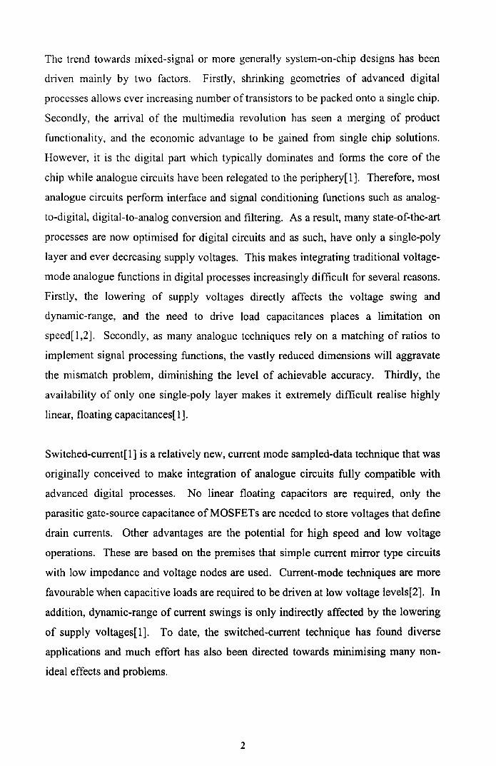
A well known algorithmic cell is the two step S2I[12] memory, shown in Fig. 2.6. In phase
¢la, the input is sampled by the 'coarse' memory transistor while the 'fine' transistor is
configured as a bias current source. When the sampling switch opens at the end of phase
¢l a, charge is injected into the storage node. In phase ¢1b, with the input still connected,
the difference between the input and stored current, which is the error current, is sampled
by the 'fine' memory transistor. The output current delivered in phase ¢2 is formed by
subtracting the 'fine' current from the 'coarse' sample. The main error from the 'coarse'
memory transistor is eliminated but there still remains a residual, signal dependent error
from the charge injected into the 'fine' memory transistor. For further refinement of the
residual error current, the n-step SnI[16] cell was proposed. Improved versions of the S2I
cell can be found in [13,14], where additional non-ideal factors were compensated for, and
where a virtual earth is produced in both the 'coarse' and the now implicit 'fine' sampling
phases. Other variants of the two-step memory cell exist which seek to reduce the
switching transient and increase available settling time[104], employ current conveyors
with reduced power dissipation[46], and operate with low voltage supplies[47].
2.4.3 Combined Algorithmic and Charge Cancellation Techniques
VDD
¢la n I¢lb~¢1~: r-L._j¢lb ___fL__¢lc __n__
¢lc,¢l I I I¢2 I I I
VSS
Figure 2.7 Combined algorithmic and charge cancellation memory cell[29]
19

As implied, these techniques employ a combination of both the Algorithmic and Charge
Cancellation techniques to eliminate the CFT errors. In [29], a second generation type cell
was proposed for total cancellation of charge injection errors as shown in Fig. 2.7. The idea
was to cancel the signal dependent errors with the n-step algorithmic technique while the
accumulated signal independent errors were then cancelled by weighted replicas.
In a similar cell[26], a single PMOS-NMOS S2I cell was used in conjunction with a dummy
circuit that cancels the signal independent CFT error of the 'fine' stage at the output. A
rather different scheme[22] that remotely resembles the S2I technique is based around a
regulated cascode second generation cell, has just an additional grounded capacitor
switched to the main storage node. The idea is to first inject half the signal dependent
charge equally into both capacitors, then open the main sampling switch to inject charge
into the main capacitor, and finally to short both capacitors to subtract the error from both
capacitors. However, imperfect cancellation will result from unequal splitting of charge
due to differences in node impedances and voltages. And because of the different loading
of the capacitors, settling performance might be affected.
2.4.4 Attenuation Techniques
Attenuation techniques aim directly to reduce the error voltage or the amount of charge that
is actually injected onto the gate of the memory transistor[103]. The most apparent way is
to increase the size of the storage capacitor. However, this will severely restrict the
operating speed of the memory cell. In one of the earliest schemes[7], a high loop gain was
created around the Miller-capacitance to minimise charge injection to the main storage node
at the opening of the switch. A second sampling switch is then opened such that the charge
injected is attenuated by capacitive division. In [20,21], a Miller capacitance enhancement
technique was used as shown in Fig. 2.8, where a small capacitor placed in the feedback
loop of an amplifier creates the effect of a large capacitance for effective attenuation of
injected charge. The loop gain is kept low during sampling and switched to high just
before the switch charge injection occurs.
20

VDD
¢1_L
¢2_L
VSS
Figure 2.8 Miller-enhanced SI memory ceU[21]
2.4.5 Zero-Voltage Switching Techniques
Signal dependent eFT errors can be eliminated by maintaining the sampling switch at a
fixed potential or 'virtual ground'. This way, the switch always opens at the same potential
and charge injection will be constant, which can then be easily eliminated. The memory
cell shown in Fig. 2.9 is based on locating the storage node at a virtual ground provided by
an operational amplifier[28]. Thus, the signal dependent charge injected is avoided.
However, high linearity is achieved at the cost of a double-poly capacitor. AMOS
capacitor can be used but will limit the signal range due to biasing requirements and will
also introduce non-linearities. A similar, fully differential cell[ 51] uses additional circuitry
to set the common-mode voltage levels at the cell input and gates of the main memory
transistors to eliminate any signal-independent charge injection.
VDD
vss
Figure 2.9 Zero-voltage switching SI sampler[28]
21

A rather unconventional memory cell configuration[34] has its summing node at the source
of the main memory transistor, which is held constant by the regulating action of a high
gain negative feedback circuit. As the switches are connected to this node, charge injection
is signal independent.
VDD
VSS
Figure 2.10 Modified grounded-gate memory cell with dummy switch cancellation[27]
In another example[27] shown in Fig. 2.10, a modified common-gate PMOS memory cell
was proposed where the sampling switch was removed from the gate of the main memory
transistor to the source side of the NMOS common gate transistor. This way, the sampling
switch is held at a near constant voltage, and any signal independent charge injection was
cancelled by a dummy switch.
2.4.6 Voltage Tracking or Adaptive Techniques
It is well known that the amount of charge injected is a function of the clock slope and
voltage levels. By adaptive control of the clock slope or voltage levels, an almost constant
eFT can be achieved. In one scheme[15,33], the clock signal level was made to track the
input signal such that a constant voltage is maintained across the sampling switch. In
another scheme[ 45], adaptive control of the clock edges combined with a dummy switch
significantly improved the cancellation of clock-feedthrough.
22

2.5 SI SYSTEMS
As with the se technique, diverse applications have also been found for the SI
methodology which include sampled-data filters[55-57,59-8l], Nyquist[89,103] and over-
sampling[47,93,94] data converters, mixers[87], comparators [88], multipliers[9l], phase
lock loops(PLLs)[90], pulse-width modulators and oscillators[92]. This section will give
an overview of the many existing SI systems. However, heavier emphasis will be placed on
filtering applications as it is more relevant to the context of this thesis.
2.5.1 SI Filters
Sampled-data filters are ubiquitous and in the realm of analogue and mixed-signal
processing, they are widely employed as reconstruction filters for AID and DJA converters,
IF filters for radio, TV, video and other front-end signal processing tasks. In recent years,
there has been a proliferation of reports on SI filter applications[55-57,59-81]. These can
broadly be classified into the following types of filters:
A. SI FIR filters
These filters are characterised by a finite impulse response and are particularly important
for applications requiring linear phase responses. An early SI FIR filter[78] employed first
generation memory cells in a tapped serial delay line configuration as shown in Fig. 2.11.
The taps were realised by scaled current mirrors at the end of each delay stage(shown
shaded), and summed together to form the output. The transfer function of the FIR filter is
given byM
H(z) =I akz-kk=O
a3
.
Figure 2.11 Tapped delay line direct FIR structure[78]
23

SI FIR filters based on differentiator elements instead of unit delays were proposed in [76].
The general transfer function ofthis type of FIR filter is given byM
H(z) =L ak (Z-I _l)kk;O
and the structure is shown in Fig. 2.12. The main advantage of the differentiator based FIR
structure over that using unit delays is that sensitivities with respect to variations in
multiplier coefficient deviations is lower when the signal-to-clock frequency ratio is less
than 1/6[76].
lin --+-r--~~- -.----+----.---I~__,
Figure 2.12 Differentiator based FIR structure[76]
In [48], elementallowpass and highpass FIR sections were proposed for video applications
which consisted of second generation memory cell based parallel delay lines. Compared to
a serial delay line, a parallel delay line requires the same number of clock phases as the
memory cells and is more sensitive to transistor mismatch. A hybrid analog-digital SI FIR
filter[58] was proposed for channel equalisation of coaxial or twisted pair cables used in 64-
QAM digital modem applications.
B. SI HR Filters
HR filters are by far the most common of all the SI filtering systems and can be realised in
many different forms. They are characterised by an infinite impulse response and realise
highly selective responses using recursive structures.
B1. Direct Form Implementations
Direct form implementations are commonly used in digital signal processing. Although
compact and straight-forward to implement, they are known to have poor sensitivity
characteristics. Therefore, few examples of SI direct form filters can be found.
24

Figure 2.13 Structure of SI HR programmable filter[81]
In [81], a fully programmable direct form filter based on SI delay-multipliers was
demonstrated. Programming, which involved changing the filter coefficients, was achieved
by connecting transistors of different sizes from an array. The HR filter structure is shown
in Fig. 2.13 and the transfer function is given by
H(z) = ___;;:_k=_.;;._O _n
l+Iakz-kke l
A direct form SI HR filter based on differentiators can be found in [76] which realises a
transfer function ofN
-bo +I bk (Z-1 -1) k
H(z) = ~=1
ao - Iak(z-l _1)kk=l
lin -+--.--__..-- -r----'---,...--"---,
l...--__'f-- -'---+-_--1.._---1---.1
Figure 2.14 Differentiator based direct form SI HR filter[76]
25

The filter structure is shown in Fig. 2.14. The advantage of using differentiators is the ease
with which highpass responses can be realised. This contrasts with integrator based filters,
which cannot be directly applied to highpass filters without modifications[76].
B2. Cascade Biquad Based
A high order transfer function can be factorised and expressed as a product of biquadratic
polynomials for pure even order functions, and in the case of an odd order function, with an
accompanying first order rational polynomial. This reduces the task of realising a high
order function into a simple cascade of 2nd order biquadratic blocks. One of the main
advantage of this type of realisation is the ease with which each biquad section, realising a
pole/zero pair, can be individually tuned. Although attractive, this decoupled nature of
cascade biquad filters results in relatively high sensitivity compared to their ladder based
counterparts. This makes them unsuitable in the realisation of high-order or high-Q filters.
An early 6th order biquad[8] based on first generation bilinear integrators was used to
demonstrate the SI technique. This was followed by a systematic procedure to design SI
cascade biquad filters from an se reference circuit. The example was based on mapping
the coefficients of a bilinear-transformed continuous time biquadratic polynomial to that of
an SI biquad structure. First generation Euler integrators were used. Similar biquads have
been fabricated with measured lowpass, highpass and bandpass responses[62].
B3. Ladder Based
Of the different ways of realising an active HR filter, ladder based designs are the most
popular. This is largely due to their low passband sensitivity characteristic, which is
inherited from simulating a passive doubly-terminated prototype. Two common forms of
simulation exist, component substitution and operational simulation.
In component substitution, the components are replaced by their synthesised, active
counterpart. The switched-transconductance(ST) technique[l] is one such example where
elements such as resistors, inductors, capacitors and composite elements can be synthesised
using a tunable transconductor and a switched-current processor. In [80], SI filters based
26

on the simulation of capacitors and transconductors of continuous-time gm-C filters were
proposed.
The majority of SI ladder filters are based on the operational simulation of a reference
prototype filter. In this method, the internal equations characterising a doubly-terminated
passive prototype are realised. The mapping between the continuous time and discrete time
domains is usually the bilinear s---+ztransform, which maps the entire left half of the s-plane
into the unit circle of the z-plane. For integrator based filters, the bilinear integrator can be
used[8,63,64,66-68], which allows a direct simulation of the transformed s-domain
prototype. With some rearrangement and modifications, Euler integrators can be used in
the so called bilinear-LDI method[69-74]. A typical doubly terminated ladder structure is
shown in Fig. 2.15, which consists of coupled two-integrator loops.
Xs1
lin
Xs XL
loutXI X2 1
Figure 2.15 Typical topology of an operationally simulated ladder filter
The I and S inputs represent integrating and summing(or feedthrough) nodes respectively.
The topology of the ladder structure is dependent on the derivation procedure employed,
and many alternatives can be obtained by matrix decomposition methods[71-73].
Individual topologies will have different salient points such as canonicity, sensitivity,
spread and total area estimate.
An alternative way of realising ladder SI filters is the based on the Wave Digital
Filter(WDF) technique[77,103]. Here, the variables simulated are the delay, transmission
and reflection occurring in waves propagating in a microwave filter. The associated
elements ofWDFs are delays and adaptors.
27

The author's contributions are in the area of SI ladder filter design for high order and
wideband filtering applications[72, 73]. Successfully proven for SC filters[ 107], it is shown
that similar benefits can be derived when the techniques are applied to SI filters. Details of
this work are documented in Chapter 3 of this thesis.
C. Delay Equalisers and Allpass SI Filters
Allpass filters have flat amplitude responses and are used primarily for group-delay
equalisation. The z-domain transfer function of an n-th order allpass filter takes the general
form
where k=-1 for n even and k=+ 1 for n odd. Although lattice and ladder based SC allpass
filters are relatively common, very few references to SI implementation can be found. In
[106], SI ladder based allpass filters were designed using second generation Euler
integrators. The structure consists of a feedforward summing network and a singly-
terminated reactive ladder shown in Fig. 2.16, and has a transfer function of
2H(z)=I---
1+ Y(z)
1
Singly-terminated -24- reactive ladder
network Y(z)
Figure 2.16 Top level structure of a ladder based SI allpass filter[106]
The author's contribution to this area are SI ladder allpass filters based on bilinear
integrators which can be designed either from an s-dornain prototype or directly in the z-
domain. Details are documented in Chapter 4 ofthis thesis.
28

D. Multirate SI Filters
The basic building blocks of multirate filters are decimators and interpolators. Decimators
decrease the sampling rate, while simultaneously performing filtering to prevent aliasing at
the lower output sampling frequency. Interpolators on the other hand increase the sampling
rate while simultaneously filtering out the unwanted images that are generated at the higher
output sampling frequency.
£la Fslin al -0 lout
a2
a3
a4
as
a6
(a) SI FIR/HR decimator SFG
(b) SI FIR/HR interpolator SFG
Figure 2.17 SFG of SI FIR/HR decimator(2x) and interpolator(2x) proposed in [82]
29

In [82], both SI FIR and HR decimators and interpolators were proposed as shown in Figs.
2.17a and b. These were based on direct form polyphase block-delayed(shown shaded)
structures using multiple input and output commutators respectively. The feedback
branches shown in dotted lines are used only in the recursive HR structures.
High speed polyphase FIR decimators for wide bandwidth video filtering applications were
proposed in [83]. A single input commutator topology was used to reduce asymmetric
clock-feedthrough errors that might otherwise produce significant distortion. For linear
phase, symmetric impulse responses, the number of multiplying coefficients can be halved
by multiplexing. This is illustrated by a linear phase, 19 tap FIR decimator(5x) with a
single commutator topology as shown in Fig. 2.18. A scheme for relaxing the timing
constraints was also proposed.
, ,...,...(A
5Fs yl al,!7 ~ rP2
~ O!21 ~rP3 Fs0------
a2,!6 ..-orA 1~ rP3 ¢2
orAI' 'N. a3,15 ~ 4- ::: rPl G0rP5 a4,14 ::: rP5
~rP5a5,!3 ,... rPl
~rP4a6,12 ~¢2
G0_-OrA°rPa7,11 ,.., 3
~rP2a8,10 ,.., rP4
('\ rPlG2)a9 ~rP5- ~
ao 18
Figure 2.18 A linear phase, 19 tap FIR decimator(5x) with a single commutator
topology[83]
In [102], an SI bandpass filter realised as a cascade of a lowpass filter clocked at a higher
rate of 72MHz and a highpass filter clocked at a lower rate of 36MHz demonstrated a
significant reduction in component spread of 86.4% and total area of 40.4% over a single
rate example. A SI single-path-frequency-translated(SPFT) narrowband (relative
bandwidth = 0.4%) bandpass filter was demonstrated using cascade biquad decimators and
30

interpolators. Compared to an equivalent single rate version, the multirate SPFT design
achieved a reduction in spread of 92.5% and total area of 91.1%, and also a significant
improvement in passband sensitivity. However, biquad structures are known to be more
sensitive than doubly terminated ladders and in the example, both the decimator and
interpolator operated at the higher sampling frequency. This makes them non-optimum in
terms of available settling time for the memory cells.
The author's contribution to this area[84-86,llO] are ladder based SI decimators and
interpolators which realise highly selective responses with transmission zeros in the
stopband, maintain low sensitivity in the passband, and operate at the lower sampling
frequency. The increased time available for the memory cells to settle enhances the
prospective high frequency operation of the circuits. Details of the proposed decimators
and interpolators are documented in Chapter 5 of this thesis.
E. N-Path and Pseudo-N-Path SI Filters
vss
Figure 2.19 Pseudo-2-path z~ -i transform resonator cell[93]
31

To date, very few, if any references can be found on the systematic design of N-path or
pseudo-N-path SI filters although they are very well established in the se technique. The
only references to SI pseudo-N-path or similar circuits are found in SI bandpass sigma-
delta(I~) modulator systems[93,94]. In [93], a pseudo-N-path resonator using the z~ -ilowpass to bandpass transform was proposed. The cell, which is shown in Fig. 2.19,
essentially consists of three second generation memory cells connected in parallel. By a
clever, but nevertheless complicated clocking scheme, the z~ _Z2 transform was achieved
to yield a transfer function of
-1-zH(z) = -2
1+ z
A different approach was taken[94] to realise z~ _z2 transformed resonators. Unlike the N-
path or pseudo-N-path techniques, the resonators were formed by a cascade of
integrators/differentiators placed in the forward path of a closed loop system as shown in
Figs. 2.20a,b to realise a Forward Euler transfer function of-2-z
H(z) = -2l+z
1;" (z) In", (z)
(a)
1;" (z) I"", (z)
(b)
Figure 2.20 Two feedback structures for realising a z~ -i transformed resonator[94]
The structure (a) uses a cascade of a Forward Euler integrator and differentiator whereas
structure (b) uses two Backward Euler integrators. A nominal feedback coefficient of R=2
32

is used. It can be shown[94] that deviation of this value, when R>2, will result in
instability of structure (a), and shifting of the resonant frequency away from a quarter of the
sampling frequency for structure (b).
The author's contribution to this area are z-+ -z transformed N-path and z-+ -itransformed pseudo-N-path fully balanced SI cells[95,111]. These cells can be used in
stand-alone configurations or in the design of N-path and pseudo-N-path SI filters via a
simple on-to-one replacement procedure. Details of these circuits are documented in
Chapter 6 of this thesis.
2.5.2 AD Converters and Miscellaneous SI Systems
Apart from filters, a diverse range of other SI applications can be found. These include
Nyquist[89,I03] and oversampling[47,93,94] AD converters, mixers[87], comparators[88],
multipliers[91], phase lock 100ps[90], pulse width modulators and oscillators[92].
2.6 INTEGRATED FILTER DESIGN AUTOMATION AND XFILT
In the race to shorten design cycles and increase integration, it is clear that pace and
progress are digital driven. Advanced and efficient tools such as VHDL or Veri log are
available to the digital designer for simulation, analysis and synthesis, to the point where
digital design is now more akin to a task in programming. In stark contrast, analogue
interface designs, while occupying a relatively small part of a mixed-signal chip, require a
disproportionate amount of time to design, test and debug. This is due to the complex
relationships that exist between circuit performance and circuit variables in analogue
designs. As a consequence, efficient analogue design tools are lagging far behind their
digital counterparts.
On the SI scene, some attempts have been made to address this problem. A CAD system
named SCADS has been introduced for the automated design of SI filters[96,97]. It uses a
knowledge based approach and a top-down methodology as shown in Fig. 2.21. The part
enclosed by a dotted-line box is the XFILT[99,lOI] filter and equaliser compiler which will
33

be discussed in greater detail later. Design specifications are first entered and
approximation routines then generate a passive RLC prototype which is used to synthesise
the block-level SI filter. At this point, a switched-netlist simulator can be used to verify for
correct ideal responses and to perform sensitivity and noise simulations. The noise
information is passed on to the transistor synthesis algorithm, where it constitutes part of a
set of design rules used for determining transistor dimensions and bias current levels.
Significant effects of interconnect capacitance and parasitics are accounted for by post
layout extraction and iteratively optimising the design using a SPICE like simulator until all
design specifications are satisfied.
Switched-netlist
NoiseSIzes
Interconnect ,-- __ -It..__ ---...
capacitance
Verify
Figure 2.21 Design flow of the SCADS SI filter design system[96]
The XFILT[99,101] filter and equaliser compiler was designed as a general filter synthesis
program capable of generating passive-RLC, active-RC, SC, gm-C and SI filters with
classical or arbitrary approximations. The design suite includes a built in general optimiser
and external sockets for interfacing to switched-network[100,108] and SPICE type
simulators. The general system structure of XFILT is shown in Fig. 2.22. The graphical
interface is based on the X11-windows[109] system while the rest of the program is written
in C. The design flow starts with the entering of desired filter specifications. In the
34

approximation step, routines are employed to fit a function to the prescribed response.
Realisation of both ladder and cascade biquad filters are possible. If the ladder option is
chosen, a passive prototype is synthesised by conventional partial/complete pole removal
methods. For active filters, the passive prototype can be realised as one of the many
possible active filter decompositions[l 07] in any of the techniques previously described. If
the cascade biquad option is chosen instead, the high order transfer function will be realised
as a cascade of second order sections with various optional pole-zero pairing strategies.
r--Gr J Specifications J'I...a 1p J Approximation 1.h 'l )
1 1c +---.( Prototype designs
{ Biquad filter design1
nt +---.( Ladder filter design
/' Simulators: '\e ~r J Filter netlist output L
SCNAP4[100],f '~ SWITCAP[108],a 1 SPICEc J Optimisation 1
'~ Je-
Figure 2.22 Design flow of the XFILT filter compiler[99,101]
A netlist of the selected filter type is produced and this can then be simulated using
SCNAP4[100] or SWITCAP[108] for switched-networks, or SPICE for continuous-time
circuits, If the design is satisfactory, the process is ended. Otherwise, the response of the
filter can be optimised and the corrected response fed back to the Approximator to generate
a new design. Throughout the entire design flow, there is constant interaction with the user
entering commands and choices via menu buttons, while design information is output via
the graphics window, and a UNIX running window in the background.
35

The contribution of the author is to the SI filter design process. Specifically, the main tasks
involved creating novel SI circuits and structures to add on to the existing SI design library,
which currently supports both single-ended or fully-differential cascade biquad and ladder
designs. Further down the structural hierarchy, the building blocks consist of integrators
and differentiators, while the memory cells can be of either first or second generation type.
Detailed information on XFILT can be obtained by consulting the reference manual[lOl].
An SI cell design automation tool named ASIMOV(A SI MOdule generation enVironment)
is described in [98], where it functions as a cell generating module within a larger SI design
system shown in Fig. 2.23. It is essentially a rule-based optimiser using analytical
equations and heuristics to fine tune cells to meet design specifications. Compared to the
SCADS[96] design system, this is a more bottom-up approach as the SI cells are first
optimised to specifications of gain error, offset etc. before being used to implement larger
SI systems.
System specifications
Behaviouralsimulation
Knowledge
Figure 2.23 SI design flow and ASIMOV[98]
36

REFERENCES
[1] C.Toumazou, 1.B.Hughes,and N.C.Battersby: 'Switched-Currents: An analogue
technique for digital technology', (Peter Peregrinus Ltd., London, UK, 1993).
[2] P. 1. Crawley and G. W. Roberts: 'Predicting harmonic distortion in switched-current
memory-circuits', IEEE Transactions On Circuits And Systems II-Analog And Digital
Signal Processing, vol. 41, pp. 73-86, 1994.
[3] D. G. Nairn and A. Biman: 'A comparative-analysis of switched-current circuits', IEEE
Transactions On Circuits And Systems II-Analog And Digital Signal Processing, vol. 43,
pp. 733-743, 1996.
[4] A. C. M. Dequeiroz and P. R. M. Pinheiro: 'Switching sequence effects in switched-
current filters', Proceedings - IEEE International Symposium on Circuits and Systems,
Chicago, Illinois, May, 1993 vol. 2, pp. 982-985.
[5] A. C. M. Dequeiroz, P. R. M. Pinheiro, and L. P. Caloba: 'Nodal analysis of switched-
current filters', IEEE Transactions On Circuits And Systems II-Analog And Digital Signal
Processing, vol. 40, pp. 10-18, 1993.
[6] P. M. Sinn and G. W. Roberts: 'Comparison of first and second generation switched-
current cells', Proceedings - IEEE International Symposium on Circuits and Systems,
London, UK, May 30-June 2, 1994, vol. 5, pp. 301-304.
[7] SJ. Daubert, D. Vallancourt, and Y.P. Tsividis: 'Current Copier Cells', Electronics
Letters, vol. 24, No. 25, pp. 1560-1562, 1988.
[8] J. B. Hughes, N. C. Bird, and 1. C. Macbeth: ' Switched currents - a new technique for
analog sampled-data signal processing Proceedings', IEEE International Symposium on
Circuits and Systems, Portland, Oregon, May, 1989, vol. 3, pp. 1584-1587.
[9] J. B. Hughes, 1. C. Macbeth, and D. M. Pattullo: 'Second generation switched-current
signal processing', Proceedings - IEEE International Symposium on Circuits and Systems,
New Orleans, Louisiana, May, 1990, pp. 2805-2808.
[10] 1. B. Hughes, 1. C. Macbeth, and D. M. Pattullo: 'Switched-Current System Cells',
Proceedings - IEEE International Symposium on Circuits and Systems, New Orleans,
Louisiana, May, 1990, pp. 303-306.
[11] M. Song, Y. Lee, and W. Kim: 'A clock feedthrough reduction circuit for switched-
current systems', IEEE Journal Of Solid-State Circuits, vol. 28, pp. 133-137, 1993.
37

[12] J. B. Hughes and K. W. Moulding: 'S2I - a switched-current technique for high-
performance', Electronics Letters, vol. 29, pp. 1400-1401, 1993.
[13] J. B. Hughes and K. W. Moulding: 'Enhanced S2I switched-current cells', Proceedings
- IEEE International Symposium on Circuits and Systems, Atlanta, Georgia, May, 1996,
vol. 1, pp. 187-190.
[14] J. B. Hughes and K. W. Moulding: 'S3I: the seamless S2I switched-current cell',
Proceedings - IEEE International Symposium on Circuits and Systems, Kong Kong, June,
1997, pp. 113-116.
[15] C. Toumazou, J. B. Hughes and D. M. Pattullo: 'Regulated Cascode Switched-Current
Memory Cell', Electronics Letters, vol. 26, No.5, pp. 303-305, 1990.
[16] C. Toumazou and S. Xiao: 'N-step charge injection cancellation scheme for very
accurate switched-current circuits', Electronics Letters, vol. 30, No.9, pp. 680-681, 1994.
[17] C. Toumazou, N.C. Battersby and C. Maglaras: 'High Performance Algorithmic
Switched-Current Memory Cell', Electronics Letters, vol. 26, No. 19, pp. 1593-1595, 1990.
[18] N.C. Battersby and C. Toumazou: 'Class AB Switched-Current Memory for Analogue
Sampled-Data Systems', Electronics Letters, vol. 27, No.lO, pp. 873-875, 1991.
[19] S. Xiao and C. Toumazou: 'Second Generation Single and Two Step GaAs Switched-
Current Cells', Electronics Letters, vol. 30, No.9, pp. 681-683, 1994.
[20] C.Y. Wu, C.C. Chen and J.J. Cho: 'Precise CMOS current sample/hold circuits using
differential c1ock-feedthrough attenuation techniques', IEEE Journal of Solid-State
Circuits, vol. 30, No.1, pp. 76-80, 1995.
[21] W. Guggenbuhl, J. D. Di, and J. Goette: 'Switched-current memory-circuits for high-
precision applications', IEEE Journal of Solid-State Circuits, vol. 29, No.9, pp. 1108-1116,
1994.
[22] D. M. W. Leenaerts, G.R.M. Hamm, M.l Rutten and G. G. Persoon: 'High
performance switched-current memory cell', Proceedings - ECCTD, Budapest, Hungary,
Sept., 1997, pp. 234-239.
[23] D. M. W. Leenaerts, A. J. Leeuwenburgh, and G. G. Persoon: 'A high-performance SI
memory cell', IEEE Journal Of Solid-State Circuits, vol. 29, pp. 1404-1407, 1994.
[24] M. Helfenstein and G. S. Moschytz: 'Clockfeedthrough compensation technique for
switched-current circuits', IEEE Transactions On Circuits And Systems II-Analog And
Digital Signal Processing, vol. 42, pp. 229-231, 1995.
38

[25] S. Lindfors and K. Halonen: 'A Novel Clock Feed-Through Distortion Cancellation
Method for SI Circuits', Proceedings - IEEE International Symposium on Circuits and
Systems, Atlanta, Georgia, May, 1996, vol. 1, pp.61-64.
[26] H. W. Cha and K. Watanabe: 'A c1ock-feedthrough and offset compensated fully-
differential switched-current circuit', IEICE Transactions On Fundamentals Of Electronics
Communications And Computer Sciences, vol. E78A, pp. 1531-1533, 1995.
[27] K. Leelavattananon, J.B. Hughes and C. Toumazou: 'Very low charge injection
switched-current memory cell', Proceedings - IEEE International Symposium on Circuits
and Systems, Monterey, California, May, 1998, pp.WPA8-6.
[28] D. G. Nairn: 'A high-linearity sampling technique for switched-current circuits', IEEE
Transactions On Circuits And Systems II-Analog And Digital Signal Processing, vol. 43,
pp. 49-52, 1996.
[29] X. Zeng, C. K. Tse, and P. S. Tang: 'Complete c1ock-feedthrough cancellation in
switched-current circuits by combining the replica technique and the n-step principle',
Analog Integrated Circuits And Signal Processing, vol. 12, pp. 145-152, 1997.
[30] T. H. Kuo, S. Y. Lee, and K. D. Chen: 'Offset current cancellation based on a
multiple-path feedback compensation (mpfc) technique for switched-current circuits and
systems', IEEE Transactions On Circuits And Systems II-Analog And Digital Signal
Processing, vol. 44, pp. 299-309, 1997.
[31] H.K. Yang and E.!. El-Masry: 'Clock Feedthrough Analysis and Cancellation in
Current Sample/Hold Circuits', IEE Proc. Pt. G, vol. 141, No.6, pp. 510-516, 1994.
[32] H. C. Yang, T. S. Fiez, and D. 1. Allstot: 'Current-feedthrough effects and cancellation
techniques in switched- current circuits', Proceedings - IEEE International Symposium on
Circuits and Systems, New Orleans, Louisiana, May, 1990, vol. 4. pp. 3186-3188.
[33] T. S. Fiez, D. J. Allstot, G. Liang, and P. Lao: 'Signal-dependent clock-feedthrough
cancellation in switched-current circuits', Proc. of China International Conf. Circuits And
Systems, Shenzhen, China, vol. pp. 785-788, June, 1991.
[34] P. Shah and C. Toumazou: 'A New high-speed low distortion switched-current cell',
Proceedings - IEEE International Symposium on Circuits and Systems, Atlanta, Georgia,
May, 1996, vol. 1, pp. 421-424.
[35] X. Hu and K. W. Martin: 'A Switched-current sample-and-hold circuit', Proceedings -
IEEE International Symposium on Circuits and Systems, Atlanta, Georgia, May, 1996, vol.
1, pp. 191-194.
39
[36] U. Gatti and F. Maloberti: 'Fully Differential Switched-Current Building Blocks',
Proceedings - IEEE International Symposium on Circuits and Systems, San Diego,
California, May, 1992, pp. 1400-1403.
[37] Y. Sugimoto: 'A 1.6V 10-bit 20MHz Current-Mode Sample and Hold Circuit',
Proceedings - IEEE International Symposium on Circuits and Systems, Seattle,
Washington, May, 1995, pp. 1332-1335.
[38] H. Traff and S. Eriksson: 'Novel Pseudo-Class AB Fully Differential 3V Switched-
Current System Cells', Electronics Letters, vol. 30, No.7, pp. 536-537,1994.
[39] H. Traff and S. Eriksson: 'Class A and AB Compact Switched-Current Memory
Circuits', Electronics Letters, vol. 29, No. 16, pp. 1454-1455, 1993.
[40] RT. Baird, T.S. Fiez and DJ. Allstot: 'Speed and Accuracy Considerations in
Switched-Current Circuits', Proceedings - IEEE International Symposium on Circuits and
Systems, Singapore, June, 1991, pp. 1809-1812.
[41] N. Tan and S. Eriksson: 'Low-Voltage Fully Differential Class-AB SI Circuits with
Common-Mode Feedforward' , Electronics Letters, vol. 30, No. 25, pp. 2090-2091, 1994.
[42] B. Pain and E.R. Fossum: 'A Current Memory Cell with Switch Feedthrough
Reduction by Error Feedback', IEEE Journal Of Solid-State Circuits, vol. 29, No. 10, pp.
1288-1290, 1994.
[43] 1. Mehr and T. Sculley: 'A 16-Bit Current SamplelHold Circuit Using a Digital
Process', Proceedings - IEEE International Symposium on Circuits and Systems, London,
UK, May, 1994, pp. 5.417-5.420.
[44]R Huang and C.L. Wey: 'A High Accuracy CMOS Oversampling Switched-Current
SamplelHold (SIH) Circuit using Feedforward Approach', IEEE Transactions On Circuits
And Systems II-Analog And Digital Signal Processing, vol. 45, No.3, pp. 395-399, 1998.
[45] S. Espejo, A Rodriguez-Vazquez, R Dominguez-Castro and J. L. Huertas: 'An
Adaptive Scheme for Feedthrough Cancellation in Switched-Current Techniues', Proc.
IEEE Midwest Symposium of Circuits and Systems, Washington DC, 1992, vol. 2. pp.
1292-1295.
[46] A. Kaiser: 'Two-step current memory cells with optimum dynamic range for advanced
CMOS technologies', Proceedings - IEEE International Symposium on Circuits and
Systems, Monterey, California, May, 1998, pp .. MAA15-14.
40

[47] P. Simek and V. Musil: 'Low voltage S2I and S3I cells for Sigma-Delta signal
processing', Proceedings - IEEE International Symposium on Circuits and Systems,
Monterey, California, May, 1998, pp. MAAI5-13.
[48] J. B. Hughes and K. W. Moulding: 'Switched-current signal-processing for video
frequencies and beyond', IEEE Journal Of Solid-State Circuits, vol. 28, pp. 314-322,1993.
[49] T. S. Fiez, G. J. Liang, and D. J. Allstot: 'Switched-current circuit-design issues',
IEEE Journal Of Solid-State Circuits, vol. 26, pp. 192-202, 1991.
[50] I. Mucha: 'Ultra low voltage class AB switched-current memory cells based on
floating gate transistors', Analog Integrated Circuits And Signal Processing, vol. 20, No.1,
pp. 43-62, 1999.
[51] J.M. Martins and V.F. Dias: 'Very Low-Distortion Fully Differential Switched-Current
Memory Cell', IEEE Transactions On Circuits And Systems II-Analog And Digital Signal
Processing, vol. 46, No.5, pp. 640-643, 1999.
[52] H. Ishii, S. Takagi and N. Fujii: 'Switched-Current circuit using fixed gate-potential
transistor and automatic tuning circuit', Electrical Engineering in Japan, vol. 126, No.3, pp.
21-29, 1999.
[53] C.K. Tse and M.H.L. Chow: 'A New Clock Feedthrough Cancellation Method for
Second Generation Switched-Current Circuits' , Proceedings - IEEE International
Symposium on Circuits and Systems, Seattle, Washington, May, 1995, pp. 2104-2107.
[54] P. Riffaud, G. Tourneur, E. Gamier and P. Roux: 'Charge Injection Error Reduction
Circuit For Switched-Current Systems', Electronics Letters, vol. 33, No. 20, pp. 1689-1691,
1997.
[55] J. B. Hughes, I. C. Macbeth, and D. M. Pattullo: 'Switched current filters', lEE
Proceedings-G Circuits Devices And Systems, vol. 137, pp. 156-162, 1990.
[56] M. Goldenberg, R. Croman, and T. S. Fiez: 'Accurate SI filters using rgc integrators',
IEEE Journal of Solid-State Circuits, vol. 29, pp. 1388-1395, 1994.
[57] R. H. Zele and D. J. Allstot: 'Low-voltage fully differential switched-current filters',
IEEE Journal of Solid-State Circuits, vol. 29, pp. 203-209, 1994.
[58] Y.L. Cheung and A. Buchwald: 'A sampled-data switched-current analog 16-tap FIR
filter with digitally programmable coefficients in 0.8j.1mCMOS', Proc. IEEE International
Solid-State Circuits Conference, San Francisco, California, Feb., 1997, pp. 54-55.
[59] E. Jonsson and B. A. Molin: 'Accurate switched-current ladder filters based on active
current mirrors', Electronics Letters, vol. 29, pp. 1840-1841, 1993.
41

[60] D. J. Allstot, T. S. Fiez, and G. Liang: 'Design considerations for cmos switched-
current filters', Proceedings of the Custom Integrated Circuits Conference, Boston,
Massachusetts, May, 1990, pp. 4p.
[61] T. S. Fiez and D. 1. Allstot: 'CMOS switched-current ladder filters', IEEE Journal of
Solid-State Circuits, vol. 25, pp. 1360-1367, 1990.
[62] T. S. Fiez, B. Lee, and D. 1. Allstot: 'Cmos switched-current biquadratic filters
Proceedings', IEEE International Symposium on Circuits and Systems, New Orleans,
Louisiana, May, 1990, vol. 3. pp. 2300-2303.
[63] J. B. Hughes and K. W. Moulding: '8MHz, 80Ms/s switched-current filter', Digest of
Technical Papers - IEEE International Solid-State Circuits Conference, San Francisco,
California, Feb., 1994, pp. 60-61.
[64] 1. B. Hughes and K. W. Moulding: 'Switched-current double sampling bilinear z-
transform filter technique', Proceedings - IEEE International Symposium on Circuits and
Systems, London, UK, May, 1994, vol. 5, pp. 293-296.
[65] M. Helfenstein, A. Muralt, G. Fischer, P. Zbinden, D. Pfaff, F. Frey and G.S.
Moschytz: 'sc and SI filters in baseband applications: a comparison', Proceedings - IEEE
International Symposium on Circuits and Systems, Kong Kong, June, 1997, pp. 297-300.
[66] N. C. Battersby and C. Toumazou: 'A high-frequency 5th-order switched-current
bilinear elliptic lowpass filter', IEEE Journal Of Solid-State Circuits, vol. 29, pp. 737-740,
1994.
[67] I. Song and G. W. Roberts: '5th order bilinear switched-current chebyshev filter',
Proceedings - IEEE International Symposium on Circuits and Systems, Chicago, Illinois,
May, 1993, vol. 2, pp. 1097-1100.
[68] A. C. M. Dequeiroz and P. M. Pinheiro: 'Switched-current ladder band-pass filters',
Proceedings - IEEE International Symposium on Circuits and Systems, London, UK, May,
1994, vol. 5, pp. 309-312.
[69] A. C. M. Dequeiroz and P. M. Pinheiro: 'Exact design of switched-current ladder
filters', Proceedings - IEEE International Symposium on Circuits and Systems, San Diego,
California, May, 1992, vol. pp. 855-858.
[70] A. C. M. Dequeiroz and P. M. Pinheiro: 'Bilinear switched-current ladder filters using
Euler integrators', IEEE Transactions On Circuits And Systems Il-Analog And Digital
Signal Processing, vol. 43, pp. 66-70, 1996.
42

[71] L. Vue and 1. I. Sewell: 'Systematic approach for ladder based switched-current filter
design', Proceedings - IEEE International Symposium on Circuits and Systems, Seattle,
Washington, April, 1995, vol. 3, pp. 2253-2256.
[72] A.EJ. Ng and J.1. Sewell: 'Feasible Designs for High Order Switched-Current Filters',
Proc. lEE Circuits, Devices and Systems, vo1.145, (5), pp.297-305, 1998.
[73] A.E.J. Ng and J.1. Sewell: 'Ladder Decompositions for Wideband Switched-Current
Filter Applications', Proc. IEE Circuits, Devices and Systems, vo1.l45, (5), pp.306-313,
1998.
[74] A.E.J. Ng and J.I. Sewell: 'Switched-Current Techniques Under Pressure:High Order
and Wideband Filter Design', Proc. 4th IEE Analog Signal Processing Colloquium, Oxford,
UK, October, 1998, ppA/1-4111.
[75] G. W. Roberts and A. S. Sedra: 'Synthesizing switched-current filters by transposing
the SFG of switched-capacitor filter circuits', IEEE Transactions on Circuits And Systems,
vol. 38, pp. 337-340, 1991.
[76] S. I. Liu, C. H. Chen, H. W. Tsao, and J. S. Wu: 'Switched-current differentiator-based
HR and FIR filters', International Journal of Electronics, vol. 71, pp. 81-91,1991.
[77] A. Rueda, A. Yufera, and 1. L. Huertas: 'Wave analog filters using switched-current
techniques', Electronics Letters, vol. 27, pp. 1482-1483, 1991.
[78] G. Liang and D. J. Allstot: 'FIR filtering using cmos switched-current techniques',
Proceedings - IEEE International Symposium on Circuits and Systems, New Orleans,
Louisiana, May, 1990, vol. 3. pp. 2291-2293.
[79] 1. Wu, Y. Hong, and G. Cai: 'New switched-current biquadratic filter', Tien Tzu
Hsueh Pao/Acta Electronica Sinica, vol. 21, pp. 70-75, 1993.
[80] 1. Schechtman, A. C. M. Dequeiroz, and L. P. Caloba: 'Switched-current filters using
component simulation', Proceedings - IEEE International Symposium on Circuits and
Systems, London, UK, May, 1994, vol. 5, pp. 569-572.
[81] M.O. Ahmad and S.H. Wang: 'A Design and Implementation of Fully Programmable
Switched-Current HR Filters', IEEE Journal of Solid-State Circuits, vol. 34, No.4, pp.
549-553, 1999.
[82] W. Ping and J. E. Franca: 'Switched-current multirate filtering', Proceedings - IEEE
International Symposium on Circuits and Systems, London, UK, May, 1994, vol. 5, pp.
321-324.
43

[83] M. Helfenstein, 1. E. Franca, and G. S. Moschytz: 'Design techniques for hdtv
switched-current decimators', Proceedings - IEEE International Symposium on Circuits and
Systems, Atlanta, Georgia, May, 1996, vol. 1, pp. 195-198.
[84] A.E.J. Ng and 1.I. Sewell: 'Switched-Current Elliptic Decimators Based on Bilinear-
Transformed Ladder Structures', Proc. 5th IEEE ICECS, Lisboa, Portugal, September,
1998, (3), pp.355-358.
[85] A.EJ. Ng and J.I. Sewell: 'Ladder Derived Switched-Current Decimators', Proc. 4th
IEE Analog Signal Processing Colloquium, Oxford, UK, October, 1998, pp.5/1-5/9.
[86] A.E.J. Ng and J.I. Sewell: 'Bilinear-Transformed Switched-Current Ladder
Interpolators', Proceedings - IEEE International Symposium on Circuits and Systems,
Orlando, Florida, May, 1999, vol. II-468, 4p.
[87] W.H.Toole,E.1. El-Masry and T.Manku: 'A novel highly linear IGHz switched-current
sub-sampling mixer', Proceedings - IEEE International Symposium on Circuits and
Systems, Atlanta, Georgia, May, 1996, vol. 1, pp. 203-206.
[88] A. Worapishet, lB. Hughes and C. Toumazou: 'Enhanced switched-current
comparator', Electronics Letters, vol. 35, No. 10, pp. 767-768, 1999.
[89] 1.S. Wang and C.L. Wey: 'A 12-bit 100-ns/bit 1.9-mW CMOS switched-current cyclic
AD converter', IEEE Transactions On Circuits And Systems II-Analog And Digital Signal
Processing, vol. 46, No.5, pp. 507-516, 1999.
[90] D.M.W Leenaerts, G.G. Persoon and B.M. Putter: 'CMOS switched-current phase-
lock loop', IEE Proceeding-Circuits, Devices and Systems, vol. 144, No.2, pp. 75-77,
1997.
[91] G. Manganaro and J.P. de Gyvez: 'A four-quadrant S2I switched-current multiplier',
IEEE Transactions On Circuits And Systems II-Analog And Digital Signal Processing, vol.
45, No.7, pp. 791-799, 1998.
[92] X. Zeng, P.S. Tang and c.K. Tse: 'New switched-current circuits for non-linear signal
processing', Proceedings - IEEE International Symposium on Circuits and Systems,
Monterey, California, May, 1998, pp.WPAI5-16.
[93] S.V. Patttamatta, P. Manapragada, V. Dalal and R. Schreier: 'A switched-current
bandpass Delta-Sigma modulator', Proceedings - IEEE International Symposium on
Circuits and Systems, London, UK, May, 1994, vol. 5, pp.477-480.
[94] lM. de la Rosa, B. Perez-Verdu, F. Medeiro and A. Rodriguez-Vazquez: 'A fourth-
order bandpass Sigma-Delta modulator using current-mode analog/digital circuits',
44

Proceedings-IEEE Instrumentation and Measurement Technology Conference, Brussels,
Belgium, June, 1996, pp. 1145-1150.
[95] A.E.J. Ng and 1.1. Sewell: 'Pseudo-N-Path Cells for Switched-Current Signal
Processing', Proceedings - IEEE International Symposium on Circuits and Systems,
Orlando, Florida, May, 1999, vol. 11-484, 4p.
[96] 1. B. Hughes, K.W. Moulding, J. Richardson, 1. Benett, W. Redman-White, M. Bracey
and R.S. Soin: 'Automated design of switched-current filters', IEEE Journal of Solid-State
Circuits, vol. 31, pp. 898-907, 1996.
[97] 1. B. Hughes and K. W. Moulding: 'Switched-current cells for design automation',
Proceedings - IEEE International Symposium on Circuits and Systems, Seattle,
Washington, April, 1995, vol. 3, pp. 2067-2070.
[98] I. O'Connor and A. Kaiser: 'Automated design of switched-current cells', IEEE
Custom Integrated Circuits Conference, Santa Clara, California, May, 1998, pp.477-480.
[99] Y.Lu, R.K. Henderson and J.I. Sewell: 'XFILT: an X-window based modern filter and
equaliser design system', Proceedings - ECCTD, Davos, Switzerland, 1993, pp. 305-310.
[100] Z.Q. Shang and J.1. Sewell: 'SCNAP4 users' guide v1.8', Department of Electronics
and Electrical Engineering, University of Glasgow, Mar. 1998.
[101] A. Ng and J.1 Sewell: 'XFILT Reference Manual and User Guide Version 3.1',
Department of Electronics and Electrical Engineering, University of Glasgow, Nov. 1997.
[102] Y. Lu and J.I. Sewell: 'Multirate SC and SI Filter system design by XFILT',
Proceedings - IEEE International Symposium on Circuits and Systems, Seattle,
Washington, April, 1995, vol. 3, pp. 2257-2260.
[103] B. Jonsson: 'Switched-current circuits: From building blocks to mixed analog-digital
systems', PhD Thesis, Department of Electronics, Electronics System Design, Royal
Institute of Technology, Stockholm, Sweden, 1999.
[104] M. Helfenstein: 'Analysis and Design of Switched-current networks', Series III
Micro-electronics, vol. 70, Hartung-Gorre, 1997.
[105] N.C. Battersby: 'Switched-current techniques for analogue sampled-data signal
processing', PhD Thesis, Department of Electrical and Electronics Engineering, Imperial
College of Science, Technology and Medicine, University of London, February 1993.
[106] Y. Lu: 'Modern VLSI analogue filter design: methodology and software
development', PhD Thesis, Department of Electronics and Electrical Engineering,
University of Glasgow, 1995.
45

[107] P. Li: 'Theory and methodology of integrated ladder filter design', PhD Thesis,
Department of Electronics and Electrical Engineering, University of Glasgow, 1990.
[108] S.C. Fang, Y. P. Tsividis and O. Wing: 'SWITCAP: a switched-capacitor analysis
program', IEEE Circuits and Systems Magazine, Dec., 1983, pp.4-9 and pp.42-46.
[109] MIT X Consortium: 'MIT X window system manual set-XII Release 5', (IXI
Limited, Cambridge, UK, 1991).
[110] A.E.1. Ng and lI. Sewell: 'Ladder Derived Switched-Current Decimators and
Interpolators', accepted, IEEE Trans. CAS II: Analog and Digital Signal Processing.
[Ill] A.E.l Ng and 1.1. Sewell: 'N-Path and Pseudo-N-Path Cells for Switched-Current
Signal Processing', accepted, IEEE Trans. CAS II: Analog and Digital Signal Processing.
46

CHAPTER3:
SWITCHED-CURRENT LADDER FILTER DESIGN TECHNIQUES
3.1 INTRODUCTION
3.2 GENERAL SI LADDER DECOMPOSITIONS
3.3 HIGH ORDER SI FILTER DESIGN
3.3.1 The Bilinear-LDI Method
3.3.2 Modified Matrix Decompositions for SI Ladder Filter Design
A. Modified Left-Decomposition Method
B. Modified Right-Decomposition Method
3.3.3 Spread Reduction For High Order Ladder Filter Design
3.3.4 Sensitivity of the SI Filters
3.4 WIDE BAND SI FILTER DESIGN
3.4.1 Switched-Current UL-LU And LU-UL Structures
A. The UL-LU Decomposition Method
B. The LU-UL Decomposition Method
3.4.2 Sensitivity Performance Comparison ofSI UL-LU and LU-UL Filters
3.4.3 SI Design Examples and Implementation Using S3I Memory Cells
A. Design of a 5th Order Elliptic Lowpass SI Filter by UL-LU Method
B. Design of a 10th Order Elliptic Wideband Bandpass SI Filter by
LU-UL method
3.5 CONCLUSIONS
REFERENCES
47

3.1 INTRODUCTION
This chapter addresses some of the design issues related to high order and wideband SI
filter design. The design of switched-current(SI} filters is a complex, multiple criteria
optimisation procedure. Some common objectives are to minimise sensitivity of amplitude
response to component variations, component value spread, total area requirement, power,
noise, and non-ideal effects. In particular, emphasis is placed on low sensitivity and low
component value spread structures.
3.2 GENERAL SI LADDER DECOMPOSITIONS
Active filters simulating the internal workings of doubly-terminated passive ladders are
well known to possess superior sensitivity to component tolerances over cascade biquad
implementations[2]. The general SI ladder derived design method is based on matrix
decompositions[9]. A passive ladder is described by the nodal equation
(sC + s·lr + G}V = J (3.1)
(where C, r and G are admittance matrices formed by the contributions of capacitors,
inductors and resistors respectively. V and J are vectors representing the nodal voltages
and input current sources). The voltage vector V is transformed into a current vector I
using a scaling resistance of In.(sC + s-Ir+ G}I = J (3.2)
A I· h bili c:. 2 1- Z-I dpp ymg tel mear-transtormation, s~ -I ' an some manipulation givesTl+z
(\jJ-IA+~B+D}I = (l+z}J (3.3)
where I is the current variable, A = (2/T)C+(T/2)r-G, B = 2Tr and D = 2G. \jJ= z-1/1-z-1
and ~ = _111_£1 represent Forward and Backward Euler integrators respectively.
The 'Left' type decompositions are obtained by factorising the A-matrix as A = AlAr to
yield
A,W= (\jJB+D}I-(l +z") J
ArI = -~W
(3Aa)
(3Ab)
48

W is an intermediate variable, introduced so that the system can be expressed as two
subsystems in terms of the operators ~ and \jJ.
'Right' type decompositions are obtained by factorising the inverse inductance matrix as B
= BIBr to yield
AI = -~(BIW+D)I+A.J
W = \jJBr
(3.5a)
(3.5b)
where A = (1+z-I)/(l-z-I) represents a bilinear integrator. Various subsets such as A = LV,
A = VL, A = lA, A = AI for 'Right' type decompositions and B = LV, B = VL, B = lA, B
= AI for 'Left' type decompositions will be used for performance comparison.
3.3 HIGH ORDER SI FILTER DESIGN
High order filters pose many design challenges. Typical obstacles facing the designer,
among many, are high sensitivity, high spreads and large chip area. In high order active
filter design, low sensitivity is crucial to preserve response accuracy, and this usually
requires the use of ladder derived realisations. Doubly-terminated passive ladders are well
known for their low sensitivity behaviour[3]. By simulating the internal workings of the
ladder filter, active circuits seek to inherit this low sensitivity property. A large
spread(> 100) in component values also increases sensitivity as it renders the design prone
to loss of response accuracy due to the finite precision of fabrication processes. At the
circuit or transistor level, enhanced memory cells[ 4,5,6] are required in practical
realisations to minimise non-ideal factors like charge injection and low conductance ratios.
In the sub-sections that follow, some of these problems are discussed and a ladder prototype
manipulation scheme[lO] is used to advantage in very high order SI filter designs, yielding
a dramatic reduction in component spread and area. Modifications to the Left- and Right-
decomposition methods[8] are presented to minimise input circuitry and also to overcome
some inherent dynamic-range scaling problems.
49

3.3.1 The Bilinear-LDI Method
The approximate-LDI method[14], when applied to ladder based designs, suffers from the
termination error problem. This gives rise to distortion in the passband which gets more
pronounced for low clock-to-signal frequency ratios. The exact-LDI method[23] on the
other hand, allows exact simulation of passive prototype filters via indirect use of LDI
variables. In comparison, the bilinear transformation is exact, as it maps the entire left half
s-plane into the unit circle of the z-plane, resulting in distortion free amplitude response and
guaranteed stability. Direct realisation of SI filters using bilinear integrators has been
demonstrated [11,12,13]. Matrix methods[8] for designing SI ladder filters using bilinear
integrators[13] have been presented. However, as this method factorises the component
matrices directly, it does not permit any manipulation of the decomposed matrices to
facilitate the removal of ill-conditioned entries that give rise to large spreads.
Alternatively, there is the bilinear-LDI method, where the bilinear transformation is used
together with Euler integrators[9,1 0, 15], to give distortion free amplitude responses even
for low clock to signal frequency ratios. The form that some of the matrices take in this
method[9,10] is amenable to manipulation which allows component value spread to be
significantly reduced.
3.3.2 Modified Matrix Decompositions for SI Ladder Filter Design
2 1- z"Beginning with (3.2), performing the bilinear transformation, s~ results inT 1+ z" '
(3.6)
Equation (3.6) can be directly implemented by bilinear integrators after decomposition[8]
into two first order sub-systems. To allow the use of LDI or Euler integrators, multiply
through the system by (1+z-1)/(I-z-1) to give
[~c+ T(1+Z-1)2r+l+Z-1 GJI= l+z-' JT 2 1- Z-I 1- Z-I 1- Z-I (3.7)
Note that
50

(I+Z_I)2 -1 4( Z-I )( -1 )1-Z-I - - 1-Z-I 1-Z-I and
l t z" Z-I1 -I = 1+ 2 I'- Z 1- Z-
substitute into (3.7) to yield
(3.8)
The system described by equation (3.8) can be decomposed for SI implementation by using
the 'Left' and 'Right' methods shown previously. 'Left' decomposition systems are
preceded by a (1+Z-I) term which needs physical implementation, while a bilinear integrator
is required at the input to 'Right' decomposition systems[9] to realise the bilinear zero at
half the clock frequency. Similar input stages are also noted in other bilinear-LDI
methods[15,16]. These can all be avoided and will result in a reduced component count,
saving on chip area and current consumption. For Left-decomposition systems, a modified
method[10] is presented, which does not involve the (1+Z-I) term but only simple feed-in
branches.
A. Modified Left-Decomposition Method
Starting with equation (3.8) as
[~C+~(1+4(I :~~')} ++21~-~-,JG}~:~~::JDivide both sides by z-I and rewrite as
(",-IA+~B+D)I = (1+z)J
where the A matrix is now A = (2/T)C+(T/2)r+G.
Factorising A=A)AT and introducing the intermediate variable W, equation (3.10) can be
(3.9)
(3.10)
expressed as
A)W= -(~B+D)1+2J
ATI= ",W+A)-I J
(3.lla)
(3.11 b)
As can be seen from (3.11a) and (3.lIb), the inputs to the modified system are now
2J and A)-I J. The input 2J is just a single feed-in branch. For (3.l1b), as J is a column
vector with only one entry in the first row, i.e. J=[ Jin 0 ... 0 ]T, a minimum of one input
branch results only if A)-I is diagonal or upper triangular. This requires A to be factorised
51

as A=IoA or A=UL, where Io=identity matrix. For A=LU and A=Alo, A,-' will be a lower
triangular or tri-diagonal matrix and this will give rise to two input branches. Details of the
modified Left decomposition derivation procedure can be found in Appendix A.
An example of a 6th order elliptic bandpass filter is given to illustrate the method. Table
3.1 lists the design data and specifications for the passive prototype shown in Fig. 3.1.
C2 C5
CB GL
Figure 3.1 6th-order bandpass ladder prototype
To compensate for the frequency warping effect of the bilinear transform, a pre-warped
scaling factor (Os= n(fplFs) was used to obtain the component values shown in Table 3.1;
fp = F/n tan(nfolFs}' f, is the filter cutoff frequency and F, is the clock frequency. The
nodal matrices describing the prototype are written as
[C2 C2
] [CnCI2
c= C2 C2+C4+C5 C5 = C21 C22 c"lC5 C5+C8 C32 C33
[Lr. + L3-' Lrl [rn r.,I' = L3-1 L3-1 + L6-1 L6-' 1 = r21 r22 r23]
L6-1 L6-1 + LTI r32 r33
[Gin 1 J:m I:[~:2]G= 0 (3.l2c) (3.l2d)GL
(3.12a)
(3.12b)
(3.12e)
Using (3.l0a), equations (3.lla) and (3.lIb) can be expanded in terms of Wand I
respectively to give
52

(3.13a)
(3.I3b)
Ull",- - - .....- -- ...
UU-I WI,'".- - - -..- - - - ,..---------.-,,,,,
Du.r : -~ - - - --
-¥Uu
D33-' - -~ - - - --VI --_ Bu ,,' Bl;,--- VJ
''' • .1
---~--" --- .... --"~I ~2
-2 BlI B32---- .... -----' loutJ
Figure 3.2 Modified Left-UL SFG for the 6th order bandpass filter
The modified Left-UL signal-flowgraph representing (3.l3a) and (3.l3b) is shown in Fig.
3.2, where the solid branches represent integrated inputs, while the dotted branches are
feed-through signals connected directly to the integrator summing nodes. The \If and -$
branches are realised by Forward and Backward Euler integrators, shown in simplified,
fully-balanced form with S2J memory cells[5] and common-mode feedforward[7] in Fig.
3.3. Transistors MI, M3, M5 and M7 form the balanced integrator pair with their
connected drains acting as the current summing node, while transistors M2, M4, M6 and
M8 serve the dual role of current source in phases t3, t5 and fine error memory in phases
t4, t6. The outputs of the integrator are mirrored by transistors M9-M12 with a scaling
factor k, representing the transconductance(gm) which is proportional to the transistor
aspect ratio(W/L). A common-mode feedforward(CMFF)[7] circuit, formed by transistors
53

NI to N5 is used to reject common-mode signals. Since the drains of NI and N2 are
connected together, twice the common-mode current is generated and is halved by setting
their transistor ratios to 0.5. This is mirrored and scaled by the PMOS transistors N3-N5 to
the output to eliminate the common-mode signals. Thus, common-mode currents which
might seriously affect biasing and dynamic range are not propagated but confined to each
block. The inputs indicated by 1+, 1-, produce Forward Euler integration when switched in
t2 and Backward Euler integration when switched in tl. Feed-through inputs connect
directly to the common summing nodes. A sample-and-hold circuit is required at the input
for proper operation with the S2I memory cells.
tlt2t3 II It4~t5~t6 II
Z-I IForward(t2 input): \jJ = k -I' Backward(tl input): ~ = -k -Il-z l-zFigure 3.3 Fully balanced S2I Euler integrator and clock waveforms
-10.00
-30.00
=-~=~ -50.00
-70.00
-90.00 J-----+-----+-----+---+------t----+--___,,__+_JO.ooE+OO 2.ooE+06 4.ooE+06 6.ooE+06 8.ooE+06 i.ooa-or 1.20E+07 1.40E+07
Frequency(Hz)
Figure 3.4 Simulated response of 6th order modified Left-UL bandpass switched-current
filter
54

The branch coefficients of the filter structure are listed in Table 3.1. Table 3.2 lists the
design statistics for the existing and modified Left-decomposition designs, showing
comparable figures for spread and total gm units. The simulated amplitude response of the
SI filter is shown in Fig. 3.4.
Table 3.1 Design data for the 6th order modified Left-UL band-pass filter
Filter specification:Lower passband edge 2.8MHz Upper passband edgeLower stopband edge 2.0MHz Upper stopband edgeStopband attenuation > 50dB Passband ripple
3.2MHz4.0MHz0.5dB
Normalised prototyPe component values:Gin = LOS C5 = 4.00037e+2L1 = 5,44037e-1 L6 = 1.15015e-2C2 = 3.61624e+1 L7 = 5.2595ge-4L3 = 5,4369ge-1 C8 = 1.78902e+4C4 = 4.08246e+2 GL = 1.9338ge-3
Transistor ratios for the modified Left-UL SI bandpass filterx7 2,4016e-01 xl7 6.779ge-02x8 8.651ge-02 xl8 6.3152e-01x9 5.9308e-01 xl9 6.2370e-01x10 7,4548e-02 x20 7.3350e-01x l l 5.09l5e-02 x21 1.6403e-01x12 6.1768e-Ol x22 1.68l5e-Olx13 8,4236e-02 x24 4.052ge-02x14 1.6372e-Ol x25 1.2835e-Olxl5 5.2138e-Ol x26 1.000x16 8.063ge-02 R27, R28 1.000
gm spread 24.67 Total gm 2365.92 unitsClock frequency 30MHz
Table 3.2 Statistics for Left-Decomposition designs
Decomposition Spread Total unitsLeft-LULeft-ULLeft-lALeft-AI
Mod Left-ULMod Left-lA
18.6022.6721.7720.6324.6725.66
2186.242670.982539.462416.502365.922447.45
55

B. Modified Right-Decomposition Method
Right-decomposition SI systems are described[9] by
(3.14)
where matrix B is factorised instead of A and ID is the identity matrix. The bilinear input
stage connects to the summing node of the first Backward Euler integrator[8,9] as shown in
Fig. 3.5a. This is not a good solution for several reasons. Firstly, using a bilinear integrator
requires the input to be sample-and-held, incurring circuitry overheads. Secondly, because
the bilinear integrator is in cascade with the rest of the ladder structure, the pole at DC
created by the denominator will make it impossible to achieve optimum dynamic-range
scaling. The bilinear integrator will saturate well before any of the Euler integrators in the
ladder structure. A better solution is to replace the bilinear integrator by a simpler (1+z")
FIR stage similar to Left-decomposition designs, which connects to the integrating input as
shown in Fig. 3.5b. This way, the zero at Fclk/Z will be realised while avoiding the pole at
DC. Alternatively, omit the input stages altogether and feed Jin directly to the integrating
input as shown in Fig. 3.5c. However, this will give rise to the familiar LDI distortion
which has to be corrected by applying an inverse weighting of lIcos(roTIZ)[17].
-1
1+ -Ik zI -I-z
-1 -1
k(1 + Z-I) k
Jin Jin Jin
(a) (b) (c)
Figure 3.5 Input arrangements for Right-Decomposition designs(a) Original bilinear input(b) Simplified bilinear input using only (1+z") stage(c) Direct input with LDI distortion resulting
56

3.3.3 Spread Reduction For High Order Ladder Filter Design
The design of practical high order filters can sometimes be hindered by large component
spreads. Take the example of an elliptic lowpass filter, with a passband ripple of s 0.2dB,
cutoff frequency of IMHz and clocked at 10MHz. Table 3.3 gives a comparison of
spreads and total gm between SI filters designed by matrix methods[8] using double-
sampled bilinear integrators[13] and cascade biquads[ 4].
Table 3.3 Design statistics for different high order SI filters
Filter Bilinear-Ladder Cascade Biguadorder gm Spread Total gm gm Spread Total gm15 >le+06 >le+06 3706.13 1463850.6617 >le+06 >le+06 12370.55 >5e+0619 >le+06 >1e+06 41286.70 >5e+0621 >le+06 >1e+06 140666.69 >5e+06
The figures obtained are clearly too large for practical implementation. Unfortunately,
neither design formulation involves the A-matrix which is key to spread reduction[1 0].
In SI circuits, transmission zeros are realised by cross-coupled branches represented by the
off-diagonal entries in the A-matrix. From the definition of A following (3.10), it can be
seen that these entries can be cancelled by letting (2/T)Cj = (T/2)Lj-1• The required
capacitance values are changed to C, = _(T2/4)Lj-1• The zeros now occur at s2= -lI(LjCj) =
4/T2 = (±2Fi on the real axis. A distortion to the filter response is thus incurred, which
can be corrected during approximation with the transmission zeros shifted to ±2F s on the
real axis. Both spread and total component count can be substantially reduced this way.
Consider the example of a 21st order elliptic lowpass video filter designed for a passband
ripple of :$; 0.6dB, cutoff frequency of 10MHz and clocked at 100MHz. The active
passband order is maintained at 21. In case (a) of Table 3.4, transistor spreads and total gm
units are tabulated for different designs with a full 21st order stopband. It can be seen that
the values are prohibitively large for practical realisation. In case (b), a pair of high
frequency transmission zero are shifted to ±2Fs on the real axis of the s-plane, leaving an
active stopband order of 19. A pair of off-diagonal elements in the A-matrix is cancelled as
a result of the negative capacitance, to yield remarkably reduced spreads and total gm units.
57

In case (c), 4 pairs of transmission zeros are shifted to ±2Fs on the real axis of the s-plane, a
13th order active stopband results and 4 negative capacitances are introduced into the
prototype ladder and lead to even lower spread figures. For the Right-LU and Right-UL
designs, this represents a reduction in spread of 99.94% and total area of 99.83%. Beyond
this, spreads for certain designs could increase and significant deterioration of transition
band steepness results. The specifications and component values of the passive prototype
filter for case (c) are listed in Table 3.5, and Fig. 3.6 shows the prototype schematic.
Table 3.4 Circuit statistics for different designs of the 21 st order lowpass filter
S: gm S)2read T: Total gm unitsLeft-LU Left-UL Left-lA Right-LU Right-UL Right-IB
(a)S 22629.69 164855.01 164852.75 24977.71 24977.65 24977.59T 328206.65 11951881.6 9162499.7 1891486.2 1891485.3 1877528.8
(b)S 132.97 49.33 50.05 58.39 58.39 58.39T 12278.80 9411.400 9076.92 13274.10 13274.10 13780.00
(c)S 47.94 23.26 23.41 14.83 14.83 27.31T 4459.35 4293.17 4114.32 3302.34 3302.34 6321.02
Table 3.5 Filter specifications and normalised component values for 21st order lowpassprototype of case( c)
Passband ripple 0.6dB Passband edge 10MHzSto)2band attenuation >50dB Sto)2band edge 10.005MHzRI 1.000 C8 9.302 C15 1.630 L22 1.924 C29 3.040C2 5.994 C9 -0.227 L16 2.945 C23 3.758 C30 9.849C3 -0.246 LlO 4.403 C17 5.627 C24 5.010 L31 0.864L4 4.066 Cl1 9.362 C18 2.743 L25 1.607 C32 1.981C5 9.071 C12 -0.226 L19 2.359 C26 3.231 R33 1.000C6 -0.230 L13 4.420 C20 4.545 C27 6.164L7 4.351 C14 7.812 C21 3.882 L28 1.358
C6 C9 CI8 C2I C24
R33
Figure 3.6 21st order passive prototype lowpass ladder filter
58

The signal flowgraph for the Right-LU decomposition design of case (c) is shown in Fig.
3.7. It can be seen that the cross-coupling feed-through branches on the left half side have
been eliminated. The 'B' and 'F' branches represent Backward Euler and Forward Euler
integrators respectively, while X78 at the input is the bilinear integrator required for Right-
decomposition designs. This was eliminated in the design, as previously discussed for the
case of Fig. 3.5c. The resulting LDI distortion was corrected by applying an inverse
weighting of l/cos(roT/2).
x78 xJ4 x35 x36 x37 x38 x39 x40 x41 x42 x43 x44 x45 x46 x47 x48 x49 x50 x51 x52 x53
BI B4
FIS
B2
FI4
B3
x74
FI2 FI3
'-J_.....,_J..--+-I-+-....L........t-I--t........,L.-+-i4-~f--I.-t__..L._..JI:....-J.......,.~--L..........x_~..Jl4.--L........,lI:_L-...,..~+---<"l Ioutx54 x55 x56 x57 x58 xS9 x60 x61 x62 x63 x64 x6S x66 x67 x68 x69 x70 x7 t x72 x73 x79
Figure 3.7 Right-LU decomposition SFG for 21st order lowpass filter
The branch coefficient values of the filter structure are listed in Table 3.6. The simulated
response of this filter implemented using the integrators of Fig. 3.3 is shown in Fig. 3.8.
Good response accuracy is observed.
Table 3.6 Transistor ratios or branch coefficients of the 21st order SI lowpass filter
X22 2.047e-Ol X37 2.938e-Ol X52 3.964e-Ol X67 3.024e-01X23 1.792e-01 X38 3.250e-Ol X53 1.603e+00 X68 3.314e-01X24 2.89ge-Ol X39 3.01ge-01 X54 2.200e-01 X69 2.928e-01X25 2.65Ie-01 X40 3.168e-01 X55 4.02Ie-Ol X70 3.641e-OlX26 3.42ge-01 X41 2.93ge-01 X56 2.835e-Ol X71 2.718e-01X27 3.385e-01 X42 4.50ge-01 X57 3.356e-Ol X72 5.957e-OlX28 3.591e-Ol X43 4.041e-Ol X58 2.97le-Ol X73 2.643e-OlX29 4.055e-Ol X44 5.032e-Ol X59 3.2l7e-Ol X74 2.972e-OlX30 3.278e-Ol X45 4.560e-Ol X60 3.027e-Ol X75 1.666e-OlX3l 4.093e-Ol X46 5.356e-Ol X6l 3.15ge-Ol X77 4.090e-OlX32 2.492e-Ol X47 5.018e-Ol X62 3.05ge-Ol X79 1.00e+00X33 2.272e+00 X48 5.418e-Ol X63 3.132e-Ol R80 1.00e+00X34 6.890e-01 X49 5.406e-01 X64 3.l13e-Ol R81 1.00e+OOX35 2.704e-Ol X50 5.l46e-Ol X65 3.085e-OlX36 3.493e-0 1 X5l 4.797e-Ol X66 3.187e-Olgm SEread 13.63 Total gm 3266.70 units Fclk lOOMHz
59

1.00 0.00
-20.000.50
-40.00- left scale= -60.00-= 0.00'-'C .-,.;
-80.00 =~ -='-'-= -0.50 CC -100.00 .;~ I-'~'"'" -1.00 -120.00~~
-1.50-140.00
-160.00
-2.00 -180.00O.OOE+OO 5.00E+06 1.00E+07 1.50E+07 2.00E+07 2.50E+07 3.00E+07 3.50E+07 4.00E+07
Frequency(Hz)
Figure 3.8 Simulated amplitude response of the 21st order lowpass filter
3.3.4 Sensitivity of the SI Filters
To estimate the sensitivity performance of the filters, the multiparameter sum sensitivity
measure defined by
(3.15)
was used to measure the sensitivity of the filter magnitude response IH(ro)1 to deviations in
transistor ratio coefficients Xi' The simulated passband sensitivity for the modified Left-UL
bandpass SI filter is plotted in Fig. 3.9 together with the sensitivities of a modified Left-lA
and existing realisations for comparison. The cascade biquad design has a relatively high
overall sensitivity while sensitivity peaks at the passband edges characterise existing Left-
decomposition[9] designs. In comparison, both the modified Left-UL and modified Left-lA
designs clearly maintain low sensitivities throughout the passband.
The computed passband sum sensitivity of the 21st order lowpass filter is plotted in Fig.
3.10. Despite the cancellation of terms and the unconventional structure, the low sensitivity
property is still preserved, which demonstrates the feasibility of realising very high order SI
filters using the spread reduction technique. These building blocks have been incorporated
60

in the filter compiler XFIL T[ 17] to enable ease of design and automatic generation of
ladder and cascade structures. This makes it possible to evaluate and compare many
different solutions to designs.
,-,~ 200 00
=-=~.;::-5 150.00til=~m='OJ 100.00o
300.00 -,-------------------------------,
250.00
-0- Modified Left-UL --<>- Modified Left-lA-- Left-UL -x- Left-IA--<>-- Left-LU -+- Left-AI- Cascade Biquad
50.00
0.00 +--------+--------+--------+-----------<2.80E+04 2.90E+04 lOOE+04 3.IOE+04 3.20E+04
Frequency(Hz)
Figure 3.9 Amplitude response sensitivities of 6th order bandpass switched-current filters
;?~ 300~-e'E 250
~.~ 200...m
500,-------------------------------~,
450
400
350
150
100
50~------------------------------------
O+------~----------_+--------,_-------+_-----~O.OOE+OO 2.00E+06 1.00E+074.00E+06 6.00E+06 8.00E+06
Frequency(Hz)
Figure 3.10 Passband amplitude response sensitivity of the 21st order lowpass switched-current filter
61

3.4 WIDE BAND SI FILTER DESIGN
Many filtering problems require wideband solutions, most notable of which are in voice
band applications. As will be shown later, a comparison of average passband sensitivity for
typical 6th order SI bandpass designs for a range of different relative bandwidths(RBW)
reveals that leapfrog[2] and coupled-biquad based structures typically suffer from
sensitivity problems at large RBWs. In this section, methods for wideband SI ladder filter
design based on the UL-LU and LU-UL matrix decompositions[10] are presented, which
preserve low passband sensitivity even for large relative bandwidths.
3.4.1 Switched-Current UL-LU And LU-UL Structures
In the UL-LU and LU-UL methods[10], both the A and the B matrices are factorised to
yield significantly different structures with unique properties. Performing the bilinear-
I': . 2 1- Z-I . (3 2) . Idtranstormation,s~---_-I ' on equation . yie sT1+z
Multiplying through by (1+z-I)/(1-z-l) gives
[3_ C + T (1 + Z-I) 2r + 1+ Z-I GjI = 1+ Z-I JT 2 1- Z-I 1- Z-I 1- Z-I (3.16)
Noting that
and
let G = GI + Gn , where GI = diag[ gil, 0 , ..... , 0] and Gn = diag[ 0 , ..... ,0, gnn ].
Then, equation (3.16) becomes
(3.17)
62

A. The VL-LV Decomposition Method
MUltiplying both sides of equation (3.17) by (l-z-I)/z-I and some rearranging yields
[~ A+$B+zD, +D,}= (l+z)J (3.18)
where
Z-I\jJ= 1 -I'-zDI =2G1,
2 TA=-C+-r-G +GT 2 1 n ,
B = 2Tr,
Here, only Euler type integrator pairso], \jJ) are used and exactness of the amplitude
response is preserved by the bilinear transform. Equation (3.18) can be realised by
introducing intermediate variables and decomposing the system into two inter-related first
order sub-systems. Derivations for these structures are aimed at preserving matrix sparsity
which translates directly to the reduced complexity of the resulting circuits.
Factorise the A and B matrices in equation (3.18) as
(3.19a)
(3.19b)
to give
(3.20)
Define
WB =VBI
Dns= DnVB-I
(3.21a)
(3.21b)
Equation (3.20) becomes
\jJ-IVALAI+ zDII + (~LB + Dns)WB= (l+z)J (3.22)
Let
WA= \jJ-I(LAI+ VA-IJ)
Dis =DILA-I
then, equation (3.22) can be arranged as
VAWA- \jJ-IJ + ~\jJ-IDlsLAI + (~LB + Dns)WB= (1 + z)J
VAWA- \jJ-IJ + ~ DlsWA- ~\jJ-IDIsVA-IJ + (~LB + Dns)WB= (1 + Z)J
VAWA- \jJ-IJ(1 + ~DIsVA-I)+ ~DlsWA+ (~LB + Dns)WB= (1 + z)J
and writing this in recursive form with respect to WA,
VAWA= -(~LB + Dns)WB - ~ DlsWA+ \jJ-IJ(1 + ~DIsVA-I)+ (1 + Z)J
(3.23a)
(3.23b)
(3.24a)
(3.24b)
63

finally combine the input tenus
UAW A= -(<jlLB + Dns)WB - <jlDlsW A+ (2+D1sUA-1)J
From (3.21 a) and (3.23a),
LA-1 (\lfWA - U/ J) = UB-1WB
(3.25)
(3.26)
The upper triangular matrix Uss and lower triangular matrix LAS are defined [10] to satisfy
the identity
UAsLA = LBSUB (3.27a)
such that
(3.27b)
rearrangmg,
(3.28)
Equations (3.25) and (3.28) describe the final system. From (3.21a), the output is now
WSn' which differs from In by only a constant as Us is an upper triangular matrix.
B. The LU-UL Decomposition Method
Multiplying both sides of equation (3.17) by (l-z") and rearranging yields
[~ A+ IjIB+z-'D, + D,} ~ (l+z-')J (3.29)
where
Z-1
\If = 1 -1 '-z1
<jl= 1 -1 '-z2 T
A=-C+-r+G -GT 2 1 n'B = 2Tr,
Factorise the A and B matrices in equation (3.29) as
A=LAUA
B =UsLs
(3.30a)
(3.30b)
to give
(3.31)
Define
WA =UAI
Dns = DnUA-1
(3.32a)
(3.32b)
Equation (3.31) becomes
64

Define
WB = \jJLBI - 2UB-IJ
Dis =DILs-I
and writing (3.33) in tenus of WB and some rearranging yields
LAW A = -~UBWB - ~ z-IDIsLBI - ~DnsWA - J
= -~UBWB - \jJDIsLBI - ~DnsWA+ 2DILB-IUB-IJ - 2DILB-IUB-IJ - J
= -~UBWB - DIsWB - ~DnsWA - 2DIsUB-IJ - J
to give the required
LAWA= -[( ~UB+ Dis) WB + ~DnsWA] - (1 + 2DIsUB-I) J
From (3.32a) and (3.34a),
(3.33)
(3.34a)
(3.34b)
(3.35)
(3.36)
(3.37)
The upper triangular matrix UBSand lower triangular matrix LASare defined[IO] to satisfy
the identity
LASUA= UBsLB
such that
rearranging (3.33),
(3.38)
(3.39)
(3.40)
Equations (3.36) and (3.40) describe the final system. From (3.32a), the output is now
WAn' which differs from In by only a constant. For lowpass filters, r is always
singular[IO], after decomposing B according to (3.30b), LBI! becomes zero and this causes
Disil in (3.34b) to become infinity. Thus, lowpass filters cannot be simulated by the LU-
UL method. Note that in both the UL-LU and LU-UL methods, no (1+Z-I) or the bilinear
(1+z-I)/(1-z-l) terms are required at either the input or output to realise the bilinear zero at
z = -1. This contrasts with the general Left and Right decomposition methods of Section
3.2. This simplified input arrangement can minimise circuit overheads, especially in low
order filters.
3.4.2 Sensitivity Performance Comparison of SI UL-LU and LU-UL Filters
It is known that the performance of bandpass filters is greatly influenced by the relative
65

bandwidth(RBW), defined as
(3.41)+ - 1/2 + .where Wm = (oi w) . wand co are the upper and the lower band-edge frequencies
respectively. Sensitivity analysis was performed for various 6th order, standard elliptic
bandpass designs for a range of RBWs. The clock-to-upper passband edge ratio is 9.375,
passband ripple O.SdB, and stopband attenuation> SOdB. The average measure of the
multiparameter statistical sensitivity over the passband is given by
1 fS = s(w)dwbandwidth passband
(3.42)
where s(to) is defined in (3.15). The results are plotted in Fig. 3.11.
100r---------~------------------------------------_,
'"CASCADE BIQUAD
LEFT-lA(Coupled-biquad)
RIGHT-LU" , (Leapfrog)~····
.- .l / ;/'"
LU-ULUL-LU LEFT-LV
10~----~---- __ ~~~~~~------ ~ __ ~~~~0.1 10
Relative bandwidth (RBW)
Figure 3.11 Average sensitivity vs RBW for 6th order SI bandpass
For RBW«l, sensitivity and spreads increase for decreasing RBW, typifying the problems
facing narrow and very narrow bandpass designs. In the mid and wide band range of
RBW> 1, both the UL-LU and LU-UL designs exhibit superior sensitivity performance over
the other designs, most significantly for very large RBWs; whilst rapid increases are
observed for the Right-LU(Leapfrog) and Left-IA(Coupled-biquad) designs. The cascade
biquad design performs poorly for RBW<4 but maintains a reasonably low average
sensitivity for large RBWs>4.
66

3.4.3 SI Design Examples and Implementation Using S3I Memory Cells
The S3I memory cell[21] operates on the same two-step principle as the S2I[5] cell but with
improved performance. The addition of a non-inverting amplifier and absence of a 'fine'
sampling switch in the new configuration produces a virtual earth input voltage on both
'fine' and 'coarse' sampling phases and gives glitch-free operation. Precision was shown to
be enhanced[21] by an order of magnitude and fewer clock waveforms are required. The
simplified S3I cell is shown in Fig. 3.12a. As the amplifier is disconnected on the output
phase, it can be multiplexed with a second cell to form an integrator as shown in Fig. 3.12b.
Forward Euler integration is obtained by switching the input in phase tl, while Backward
Euler integration is achieved by simply changing the input phase to t2(shown in
parenthesis). Feedthrough signals are fed directly to the summing node S. Transistors P3
and N3 form the scaled mirror output of the integrator. The associated clock waveforms are
shown in Fig. 3.12c.
t2~lout Iin o-------t1(t2)
lout
VDD
VSS VSS
(a) (b)
tl It2 .....1 _---'t3 rI It5 ____r-"l_
(c)
Figure 3.12 S3I building blocks
(a) S3I memory cell
(b) Basic S3I Euler integrator
(c) Integrator clock waveforms
67

A. Design of a 5th order elliptic lowpass SI filter by UL-LU method
C3 C6
Figure 3.13 5th order elliptic lowpass passive prototype
The passive prototype used is shown in Fig. 3.13. The component matrices and variable
vectors representing the nodal equations are written as
[C2+C3 -C3 ] [Cn C!2C= -C3 C3+C5+C6 -C6 = C21 Cn C,,]
-C6 C6+C8 C32 C33
[ U'-L4-1 1 [rn fl2
[= -L4-1 L4-1 + LTI -LTI = [21 f22 r,,]-LTI LT! f32 f33
[G" [J" ] V~[~:JG= o ]~G' +G, J= 0
GL 0
(3.43)
Similarly, expanding (3.28) in terms ofWB gives
(3.44)
The signal flow graph representing equations (3.43) and (3.44) is shown in Fig. 3.14. The
\l' and ~ branches are realised by Forward and Backward Euler integrators respectively.
68

Solid line branches connect to the integrator inputs lin. The branches shown in dashed
lines, representing feed-through signals, connect directly to the common summing node, S,
of the integrators. Table 3.7 lists the design data for the lowpass filter and the circuit is
given in Fig. 3.15.
-UASlliUAII UAl2iUAII UA23iUA22
~"""'~""" ,.\:'.,' .... ',. "'. .."" ..... " ".. .WA}'" ". WA2 .: ' ". WA3.. ..
/ UASII UASI2 UAS22 UAS23 UAS33
DisilUAII'I~ LBSII,I\jJ .~UA22'1~ L
BS22,1\jJ ~UA33'1~ ,
LBs33,I
~UBI1 UBI2 UB22 UB23 Dns33
- - "" ....""-.W01••••
... ..··WR2 '.. ' .
Iour
..... ~ ......LsS2 tlLBS22
.....~ .....LsS32/LBS33
Figure 3.14 UL-LU signal flow graph for the 5th order SI lowpass filter
Figure 3.15 5th order UL-LU SI lowpass filter
69

Table 3.7 Design data for the 5th order lowpass filter
Filter specification:Upper passband edge IMHz Stopband edge 1.667MHzPassband ripple O.603dB Clock frequency IOMHz
Normalised values for the passive prototype:Rin 1.000000e+00 L4 3.427935e+00C2 S.266390e+00 C5 7.200S12e+00C3 3.40739Ie-01 C6 9.24284ge-01
Stopband attenuation>45.8dB
L7 2.985822e+OOC8 4.770045e+00RL 1.OOOOOOe+OO
Transistor ratios for the SI UL-LU filter:x7 2.129816e-01 xiS 2.09797Ie-01x8 9.524698e-02 xI6 3.692527e-01x9 4.120537e-OI xI7 3.993545e-OlxlO 1.064174e+00 xI8 3.030140e-OlxII 3.S64073e-OI xI9 8.76494ge-Olx12 3.34417ge-Ol x20 7.714552e-02xl3 6.289623e-O I x21 S.18170ge-01xl4 3.95458ge-01 x22 9.327838e-02
x23 1.07242ge+00x24 1.000000e+00R26 1.00000e+00R27 1.OOOOOe+OO
gm spread 13.90Total gm 1434.8 units
Simulations were performed using SCNAP4[22] with the various circuit parameters set as:
gain of the operational amplifier(A)= 100, bias voltage(Vret)=half rail-to-rail voltage,
output conductance of transconductorsig.)= Ie'5S, switch on-resistance(Ron)= lOOn, switch
off-resistancerkoffj=Ie'f ' Q. The gain response with the filter clocked at IOMHz is shown
in Fig. 3.16.
0.00
-10.00
-20.00
-30.00
""0.00=:~ -5000".;c
-60.00
-70.00
-80.00
-90.00
-ioo.ooO.OOE+oo 1.00E+06 2.00E+06 3.00E+06 4.00E+06 S.OOE+06
Frequency(Hz)
Figure 3.16 Simulated gain response ofSI UL-LU lowpass filter
70

A simulation of passband sensitivities for various other lowpass filters is compared to the
UL-LU design in Fig. 3.17. Both the Left-LU and Left-IA(Coupled-biquad) designs suffer
from peaks in sensitivity towards low frequencies and at DC. The Right-LU(Leapfrog)
design maintains low sensitivity throughout the passband but at a level higher than the UL-
LU design. The cascade biquad design shows good low frequency sensitivity but increases
significantly towards the passband edge. The UL-LU design clearly exhibits superior
sensitivity performance.
45.00
LEFT-LA
40.00
(Coupled-biquad),.... 35.00·~='0~ 30.00
:~'r;;=OJVJ 25.00
LEFT-LV
RIGHT-LU'-,
20.00 LooooOQQ<l,!,!, ,~, ,00.. <>", ,<>0, ,<>0, .<>0, ,~, ,.;c, ,~. ,~, :~. ,~: :~~~~1OOO<;OO.,.)()OO',c:P"'"
'" , ~, , .CASCADE BIQUA' .......·
r,
UL-LU
:'
2.00E.05 4.00E·OS 6.00E·OS15.00 +------+------+------+------+------1
O.OOE.OO 1.00E.06
Frequency(Hz)
B.OOE.OS
Figure 3.17 Passband sensitivity comparison for the SI UL- LU lowpass filter
The simulated noise performances given 111 Fig. 3.18 show the UL-LU, and Left-
Decomposition designs suffering from higher noise in the passband and at low frequencies.
Table 3.8 gives a comparison of the implementation costs and supports the conclusion that
the UL-LU design offers the best solution to this lowpass problem.
Table 3.8 Circuit statistics for different designs of 5th order lowpass filter
Decomposition Transistorspread
Total gm(units)
LEFT-LULEFT -IA(Coupled-biquad)RIGHT-LU(Leapfrog)UL-LUCASCADE BIQUAD
17.14159317.57768218.24594213.9013719.573100
71
1814.1808791828.3398442702.5410951434.7726831190.366058

-100.00 -,+-----------------------------,
-110.00
~'-'...6- -120.00'"--,-.,~'0
>' -130.00C'r;;=<j,j'0 -140.00';I....(.j<j,j
~ -150.00<j,j
'"'Qz;
-160.00
UL-LU,LEFT-LU,LEFT-IA(Coupled-biquad)
:::::::::::::....r',,'..".::..,RIGHT-LU(Leapfrog),CASCADE BIQUAD ...""""""",::::::::::: ...
---::::
-170.00 +-------+------+------+-------+------1O.OOE+OO 5.00E+03 1.00E+04 l.SOE+04 2.50E+042.00E+04
Frequeucyflfz)
Figure 3.18 Typical simulated noise performance of SI lowpass filters with 10-band
foldback effects
B. Design of a 10th order elliptic wideband bandpass SI filter by LU-UL method
C13 RH
Figure 3.19 10th order elliptic bandpass passive prototype
The synthesised passive prototype shown in Fig. 3.19 is a quasi-elliptic filter, with all the
lower stopband zeros shifted to the origin to reduce the spread. The relative bandwidth of
the filter is 3.62. The design specifications are listed in Table 3.9.
72

Table 3.9 Design data for l Oth order bandpass filter
Lower PB edge 80kHzLower attenuation 40.5dBPassband ripple 1.7dB
RI 1.000000E+OOL2 1.535371E+OIC3 4.374470E+OIL4 1.005315E+OIC5 4.944113E+OI
XII 6.l2772ge-OIXI2 2.284462e+OOX13 6.l90005e-OIX14 5.988833e-OlXI5 2.654423e-OIX16 1.161250e-OlXl7 6.l77562e-02XI8 1.649996e-OIXI9 6.311456e-OIX20 8.II2347e-OI
Filter specification:Upper PB edge 1.2MHzUpper SB edge 1.34MHzFc10ck IOMHz
Lower SB edge 46.8kHzUpper attenuation 37dB
Normalised values for the passive prototype:C6 5.591399E+OO Lll 1.178033E+OOC7 5.96634IE+OO LI2 9.325125E+OOL8 8.00973IE-OI C13 9.031556E+OOC9 7.961073E+OO RI4 7.351160E-OICIO 2.303288E+OO
Transistor ratios for the SI LU-UL filter:X2I 3.856926e-OI X3I 5.4I7323e-OIX22 1.204070e+OO X32 1.2561I4e+OOX23 8.91474ge-OI X33 2.709830e-OlX24 5.006653e-02 X34 l.043100e-OlX25 1.27338Ie-01 X35 8.099850e-OlX26 2.971864e-Ol X36 7.691110e-OlX27 5.281544e-01 X37 1.000000e+00X28 2.913257e-OIX29 5.357777e-OIX30 2.504443e-OI
'.
gm spread 45.63Total gm I080.9 units
After deriving the component matrices and applying equations (3.30), (3.32), (3.39), the
resulting signal flow graph corresponding to (3.36) and (3.40) is shown in Fig. 3.20. The
SI realisation of the LU-UL bandpass filter is shown in Fig. 3.21 and its simulated gain
response in Fig. 3.22.
·2Uesl/Uellr •• ~ ••• ...---...,._,
LA2I/LA22....~..-. LA4)/LA44
....~..-, LASiLAS5....~..-.LAn/LA))
,,,.~..-,"
.:"
LAS)) LAs4) LAS44 LASS4 LASSS \~\jJ UBS4/\jJ UBSSS·11jI
LA))·11jl LA44·11jl LASS·11jl
00555
UB)) UB)4 UB44 UB45 UBS5. ,
10
. ..': ••.•. ~ ..• J" ••• <I••• '
'(I+2DISIIUBII·I) UBSI2/UBSII
.' '" _ .' ••• <I ••• '
UBS23/UBS22
..........UBS45/Uesss
...........UBS)4/UBS))
Fig.3.20 SI LU-UL signal flow graph for the 10th order bandpass filter
73

XJe
XJ5
Figure 3.21 10th order LU-UL SI bandpass filter
74
lOut

-20.00
~:::.,C -40.00-;C)
-10.00
-30.00
-60.00
-50.00
-70.00
-80.00 -11------+------+-------+------+-----11O.OOE+OO 1.00E+06 2.00E+06 3.00E+06 4.00E+06 5.00E+06
Frequency(Hz)
Figure 3.22 Simulated gain response ofSI LU-UL bandpass filter
The passband sensitivity comparison of the LU-UL versus other designs is plotted in Fig.
3.23. The cascade biquad design has a large overall sensitivity which increases
dramatically towards the upper passband edge. Similar peaks are observed in the vicinity
of the upper passband edge for the Right-LU(Leapfrog) and Left-IA(Coupled biquad)
designs. Near the lower passband edge, both the Left-IA(Coupled biquad) and Left-LU
designs exhibit sensitivity peaks. It is apparent that both the UL-LU and LU-UL designs
maintain low sensitivity throughout the passband.
The comparison of simulated noise behaviour in Fig. 3.24 demonstrates superior noise
performance of the LU-UL and UL-LU designs, which translates to improved signal-to-
noise ratios. Table 3.10 gives a comparison of the implementation costs for different
designs. Both the UL-LU and LU-UL designs show reasonable and comparable transistor
spreads and total gm values. Note that in all the designs, the prototype component values
have been scaled by a factor of COs = n(f/F s) to compensate for the frequency warping
effect of the bilinear transform, where fp= F/n tan(nfolFs), f, is the filter cutoff frequency
and F, is the clock frequency. Scaling for maximum dynamic range and minimum
spread[9] has been performed to obtain the transistor ratios of the SI filters. The design
routines for these SI UL-LU and LU-UL structures have been incorporated into the filter
75

and equaliser compiler XFILT[17], where the synthesis process, including pre-warping and
scaling are automatically carried out.
80.00
70.00
,-, 60.00 .-~e-..cc'0
E 50.00 ..;;.::.;;;=~(/J 40.00
30.00
r-.! \j \
./ 1
Ifttii,i(
LU-ULUL-LU
20.00 +-_::_-=~~~='::--+-----+------+------+---_j7.00E+04 2.70E+05 4.70E+05 6.70E+05 8.70E+05 1.07E+06
Frcqucncy(Hz)
Figure 3.23 Passband sensitivity comparison for the SI bandpass filters
II....\ /<..
LEFT-IA(Coupled-hiquad) /" ~- /
\ ~\ /"-CASCADE BfQUAD\ -, / I".
<; ./ / ....--1--- I- ,/ ./'"....._ ./ _". <, /
-<~:~~><~/ ,/ ,_/____ --- .... RIGHT-LU(Leapfrog)
·120.00
·122.00
'N' ,::c -124.00 \'-'...... Ir;;r~ -126.00cc'0'-';;>
-128.00a.;;;=~ -130.00'0
-;......... ·132.00~c..Cl'~Cl' -134.00'QZ
-136.00
·138.007.00E+04
\ ..\ / ",-LEFT-LU. // -x-x "., /~....
x
2.70E+05 4.70E+05 6.70E+05 8.70E+05 1.07E+06
Frequency(Hz)
Figure 3.24 Typical simulated noise performance of SI bandpass filters with 10-band
foldback effects
76

Table 3.10 Circuit statistics for different designs of 10th order SI bandpass filter
Decompositions Transistorspread
Total gm(units)
LEFT-LULEFT -IA(Coupled-biquad)RIGHT -LU(Leapfrog)CASCADE BIQUADUL-LULU-UL
28.2768.1033.831125.3257.0445.63
3.5 CONCLUSIONS
1007.002230.101501.825306.931776.501080.91
The design of high order SI filters and its associated problems have been explored. In
particular, effort was focused on obtaining low sensitivity, low spread structures with
reduced number of components. To this end, modified Left- and Right-decomposition SI
structures have been introduced with improved sensitivity and simple input stages. Using
prototype ladder and matrix manipulation, quite remarkable reductions in spreads and total
gm were achieved for a 21st order elliptic lowpass filter, while preserving low passband
sensitivity. In the process, the number of cross-coupling feedthrough branches for realising
transmission zeros are reduced, further simplifying the resultant filter structure. This paves
the way for the feasible realisation of high-order SI filters. Fully-balanced SI Euler
integrators using S2I cells were used in the simulation of all the filters.
The design of wideband switched-current UL-LU and LU-UL filters by matrix methods
have been presented. The procedure was derived and demonstrated for a 5th order lowpass
and a IOth order bandpass example implemented using S3I Euler integrators. These filter
structures do not require additional input stages to preserve the exact bilinear mapping; they
utilise simple Euler integrators, and allow low clock-to-cutoff frequency ratios. Sensitivity
simulations reveal that low passband sensitivity is maintained even for large relative
bandwidths. This, together with low passband noise, make these structures ideally suited
for wideband bandpass designs. The UL-LU design has also demonstrated superior
sensitivity and implementation efficiency in the lowpass design.
77

REFERENCES
[1] J. B. Hughes, N. C. Bird and 1. C. Macbeth: ' Switched currents - a new technique for
analog sampled-data signal processing Proceedings', IEEE International Symposium on
Circuits and Systems, Portland, Oregon, May, 1989, vol. 3, pp. 1584-1587.
[2] R.Gregorian and G.C. Ternes: 'Analog MOS Integrated Circuits for Signal Processing',
(Wiley, New York, 1986).
[3] H.J. Orchard: 'Inductorless filters', Electronics Letters, vol. 2, pp. 265-270, 1966.
[4] C.Toumazou, J.B.Hughes,and N.C.Battersby: 'Switched-Currents: An analogue
technique for digital technology', (Peter Peregrinus Ltd., London, UK, 1993).
[5] J. B. Hughes and K. W. Moulding: 'S2I - a switched-current technique for high-
performance', Electronics Letters, vol. 29, pp. 1400-1401, 1993.
[6] P. Shah and C. Toumazou: 'A New high-speed low distortion switched-current cell',
Proceedings - IEEE International Symposium on Circuits and Systems, Atlanta, Georgia,
May, 1996, vol. 1, pp. 421-424.
[7] N. Tan and S. Eriksson: 'Low-voltage fully differential class-AB SI circuits with
common-mode feedforward', Electronics Letters, vol. 30, pp. 2090-2091, 1994.
[8] Y. Lu: 'Modem VLSI analogue filter design: methodology and software development',
PhD Thesis, Department of Electronics and Electrical Engineering, University of Glasgow,
1995.
[9] Y. Lu and J. 1. Sewell: 'Systematic approach for ladder based switched-current filter
design', Proceedings - IEEE International Symposium on Circuits and Systems, Seattle,
Washington, April, 1995, vol. 3, pp. 2253-2256.
[10] P. Li, R.K. Henderson and J.I. Sewell: 'A methodology for integrated ladder filter
design', IEEE Transactions on Circuits and Systems, vol. 38, no. 8, pp.853-868, 1991.
[11] I. Song and G. W. Roberts: '5th order bilinear switched-current chebyshev filter',
Proceedings - IEEE International Symposium on Circuits and Systems, Chicago, Illinois,
May, 1993, vol. 2, pp. 1097-1100.
[12] N. C. Battersby and C. Toumazou: 'A high-frequency 5th-order switched-current
bilinear elliptic lowpass filter', IEEE Journal Of Solid-State Circuits, vol. 29, pp. 737-740,
1994.
78

[13] 1. B. Hughes and K. W. Moulding: 'Switched-current double sampling bilinear z-
transform filter technique', Proceedings - IEEE International Symposium on Circuits and
Systems, London, UK, May, 1994, vol. 5, pp. 293-296.
[14] L.T. Bruton: 'Low sensitivity digital ladder filters', IEEE Trans. CAS, vol. 22, pp.16S-
176, 1975.
[15] A C. M. Dequeiroz and P. M. Pinheiro: 'Bilinear switched-current ladder filters using
Euler integrators', IEEE Transactions On Circuits And Systems II-Analog And Digital
Signal Processing, vol. 43, pp. 66-70, 1996.
[16] A C. M. Dequeiroz and P. M. Pinheiro: 'Switched-current ladder band-pass filters',
Proceedings - IEEE International Symposium on Circuits and Systems, London, UK, May,
1994, vol. 5, pp. 309-312.
[17] Y. Lu, R.K.Henderson and 1.I.Sewell: 'XFILT: an X-window based modem filter and
equaliser design system', Proceedings - ECCTD, Davos, Switzerland, 1993, pp. 305-310.
[18] Z.Q. Shang and 1.1. Sewell: 'Development of efficient switched network and mixed-
mode simulators', Proc. IEE-Circuits, Devices and Systems, vol. 145, no. 1, pp. 24-34,
1998.
[19] T. S. Fiez and D. J. Allstot: 'CMOS switched-current ladder filters', IEEE Journal of
Solid-State Circuits, vol. 25, pp. 1360-1367, 1990.
[20] J. B. Hughes and K. W. Moulding: 'SMHz, 80Ms/s switched-current filter', Digest of
Technical Papers - IEEE International Solid-State Circuits Conference, vol. pp. 60-61,
1994.
[21] 1.B. Hughes and K.W. Moulding: 'S3I: the seamless S2I switched-current cell',
Proceedings - IEEE International Symposium on Circuits and Systems, Kong Kong, June,
1997, pp. 113-116.
[22] Z.Q. Shang and J.1. Sewell: 'SCNAP4 users' guide vl.8', Department of Electronics
and Electrical Engineering, University of Glasgow, Mar. 1998.
[23] R.B. Datar and AS. Sedra: 'Exact design of strays-insensitive switched-capacitor
ladder filters', IEEE Transactions on Circuits and Systems, vol. 30, no. 12, pp. 888-898,
1983.
79

CHAPTER4:
DESIGN OF SWITCHED-CURRENT BILINEAR GROUP-DELAY EQUALISERS
4.1 INTRODUCTION
4.2 DESIGN METHODS FOR BILINEAR INTEGRATOR BASED ALLPASS
SWITCHED-CURRENT LADDER FILTERS
4.2.1 s-Domain Approach
4.2.2 z-Domain Approach
4.3 SI SIMULATION USING BILINEAR INTEGRATORS
4.3.1 Design Example of a Switched-Current Filtering System: Cascade of a 3rd
Order Lowpass and a 6th Order Allpass Delay Equaliser
4.3.2 Sensitivity and Non-ideal Factors
A. Sensitivity
B. Non-ideal Factors
4.4 CONCLUSIONS
REFERENCES
80

4.1 INTRODUCTION
Allpass filters are primarily used for group-delay equalisation for applications which
require linear or near-linear phase characteristics. However, as the allpass transfer function
is non-minimum phase by definition, low sensitivity ladder simulation remains a problem.
As such, most allpass functions have hitherto been implemented either as lattice
structures[ I] or as cascades of biquadratic sections[2]. A novel method for digital allpass
filter design was previously proposed[3-5] which allowed the allpass function to be realised
as the sum of a constant term and a ladder-realisable, reactive driving point impedance.
The main advantage of this method is low sensitivity to component variation, achieved with
low sensitivity ladder structures and the inherent structurally loss less property. This method
was subsequently extended to include switched-capacitor[ 4,6] and switched-current[7]
forms. These were however implemented either by Lossless-Discrete-Integrator(LDI)
transformed structures, or Bilinear transformed structures with Euler integrators in the so-
called Bilinear-LDI method. With the Bilinear-LDI method, use of the bilinear transform
ensures 'exact' responses and low Fs/fo ratios. However, Euler integrators suffer from
excess phase which should ideally be cancelled when employed in a two-integrator loop
configuration. Therefore, it is highly desirable to derive structures that allow the use of
bilinear integrators which do not suffer from excess phase and directly implements the
bilinear-transform.
In this chapter, two approaches are presented for deriving SI allpass structures in terms of
the bilinear integrator. The first proceeds via the s-domain while the second is a direct z-
domain approach. The respective continued-fractions expansions are used to synthesise a
prototype which can then be simulated using standard matrix methods[7]. The structurally
lossless property of the singly-terminated reactive ladder section implies zero sensitivity
contribution to the amplitude response of the equaliser. This is important as it minimises
distortion to the amplitude response of the filter being equalised. Significant improvements
in overall amplitude and group-delay sensitivities are made over existing Euler integrator
based ladder realisations. Simulations of various non-ideal effects also reveal the merits of
different designs.
81

4.2 DESIGN METHODS FOR BILINEAR INTEGRATOR BASED ALLPASS
SWITCHED-CURRENT LADDER FILTERS
4.2.1 s-Domain Approach
An allpass transfer-function in the s-dornain has poles and zeros in mirror image symmetry
and is written as
H(s) = ± P(-s)pes)
It can be shown[3] that (4.1) can be written with
EvP(s)
)'(s) = ()un?(s)()un?(s)
(4.1)
for n even(4.2)
for n oddEvP(s)
for the Hurwitz polynomial
pes) = EvP(s) + Qun?(s) (4.3)
as
Hts)= 1- )'(s) = 1- 21+ Yrs) 1+ Yts)
(4.4)
Y(S) represents the reactive driving point admittance, from which the passive prototype can
be synthesised using continued-fractions expansion(CFE)[12]
1)'(s) = Cls+-----1---
LIS + ----1--C2s+----
1C s+- (4.5)m Lms
Thus, in general, Yts) can be expressed in matrix form using nodal formulations[6] as
Yes) = sC+s-1[,+G (4.6)
where C, T and G are matrices formed by the contribution of capacitors, inductors and
resistors respectively. Performing the bilinear transformation
82

(4.7)
. h 1-1 z-1WIt /l, =--
z+1(4.7a)
results in
Y(z)= J/V1= X1C+Ar+G
Hence, (4.4) can be written as
2H(z)=1----
1+ Y(z)
(4.8)
(4.9)
which can be realised as shown in Fig. 4.1. The general structure of the synthesised Z(z) =
1/Y(z) driving point function is shown in Fig. 4.2.
a
Vin
1 -b0 ro.
I ~
I Z(z)=IIY(z) II~ o
Vout
a = 1.0, b = 2.0
Figure 4.1 Top level realisation of the allpass function
For s-dornain: Yi= SCi, z, = sl.,
For z-domain: Yi = A.-ICi, z, = A.-ILj
Figure 4.2 Typical structure of a synthesised driving point irnmittance function
83

4.2.2 z-Domain Approach
The transfer function for an n-th order allpass structure in the z-domain takes the general
form of
(4.10)
with k = -1 for n even, k = +1 for n odd.
This can be rearranged and expressed as
H(z) = 1- P(z) - ZIlP(Z-I)P(z)
(4.11 )
= 1- 2__ -:-1+ P(z) + ZIlP(Z-I)
P(z) - ZIlP(Z-I)
(4.12)
Thus,
2H(z)= 1----
1+ Y(z)
h Y( ,I P(z) + Z"P(Z-')were z/= __:_....:...._-__:____..:...P(z) - ZIlP(Z-I)
(4.13)
(4.14)
Utilising a continued fractions expansion(CFE) method in [9], the reciprocal of (4.14), i.e.
Y(Z-I) can be expanded in terms of the bilinear operator
A-I = z -1z+1
(4.15)
as
Y(Z-l) = C1KI + 1 _L1K' + 1 _
CzA-l + __ 1__
(4.16)
1
Thus, Y(z) can be represented by the ladder part of Fig. 4.2 and expressed in matrix form
using nodal formulations as
Y(z)= J/V1= X1C+A[,+G (4.17)
which is identical to the expression in (4.8) for the s-domain approach.
84

4.3 SI SIMULATION USING BILINEAR INTEGRATORS
After determining the allpass structure and obtaining the z-domain description of the
singly-terminated reactive section in terms of the bilinear integrator, simulation of the
structure can proceed using conventional matrix methods[7] as follows:
From (4.8) or (4.17),
(XIC+Ar+G)V=J (4.18)
Using a Inscaling resistance, the voltage variable is changed to a current variable as
(Xl c+Ar+G)I=J
Let r = rLrR
(4.19)
(4.20)
Defining W = Ar RI ,
and substituting (4.20) and (4.21) into (4.19) yields
CI= -A(r LW+GI) + AJ
(4.21 )
(4.22)
The system of equations (4.21) and (4.22) together describe the operational simulation of
the reactive section of the allpass structure. I'LrR can be obtained by either the LU-
factorisation (T = r Lr u, r = r ur d or direct methodstl" = lor, I'= rlo)[7], where ID is the
identity matrix. The remaining functions of summation and scaling by a factor of 2.0 in
Fig. 4.1 can be easily implemented in the SI realisation as will be shown in the example of
a 6th order group-delay equaliser for a 3rd order lowpass filter.
4.3.1 Design Example of a Switched-Current Filtering System: Cascade of a 3rd
Order Lowpass and a 6th Order Allpass Delay Equaliser
Cl L8
Figure 4.3 6th order singly-terminated allpass ladder prototype
85

Table 4.1 Design data for the 6th order allpass filter
Specification of the delay equaliser
Equalisation edge frequency 1MHz In-band ripple <0.06uSec.
Approximation type
Sampling frequency
Equiripple
5MHz
Filter order 6
Poles and zeros of the allpass transfer function in the z-domain
1.372567±jO.1804098
1.266440±jO.5030 130
1.117817±jO.7937362
z-domain poles
0.7161887±jO.0941356
0.6820213±jO.2708898
0.5947315±j0.4223052
z-domain zeros
Normalised prototype component values
Gin 1.00000 C2 -0.251444 C4 5.109904
Cl 1.826231 L3 3.977036 C5 -0.167138
L6 5.983064 C7 7.439028 L8 10.54152
Transistor ratios for the SI aUpass filter
Xin 0.6350079 X12 0.2116817 X18 0.1683081
X7 0.1607860 X13 0.2116782 X19 0.1799743
X8 0.0532250 X14 0.1277082 X20 0.1021482
X9 0.0380966 X15 0.1277082 X21 0.6350065
X10 0.0214943 XI6 0.2514389 Spread: 93.1
XII 0.6501820 XI7 0.2531990
Consider the singly-terminated allpass ladder prototype shown in Fig. 4.3. By forming the
respective component matrices according to (4.8) and applying (4.21), (4.22) with (4.20)
as er = FLru) results in the SFG for the allpass filter as shown in Fig. 4.4, where the
dashed-lines represent feedthrough(ft) branches. The design specifications for the allpass
filter and corresponding coefficient values after scaling for maximum dynamic range and
minimum spread are listed in Table 4.1. The conventional single sampling(SS) bilinear
integrator[13] is shown in Fig. 4.5 while Fig. 4.6 shows the double sampling(DS) version
proposed by Hughes and Moulding[8]. Double sampling allows the clock frequency to be
halved compared to single sampling.
86

Vout b XI6 Xl7 XI8 Xl9 X200
( X8 X7.· ·.XlO X9''. .. .. ..A A A
a X2I .. ..
\A A A
~~VinXin XII XI2 Xl3 X14 XIS
Reactive ladder section
1+ Z-Ia =1.0, b = 2.0, "-=-1---1-z
Figure 4.4 SFG for the 6th order allpass ladder filter
lout
H(z) = k 1+ Z-I
1 -I-z
Figure 4.5 Single-sampling(SS) bilinear integrator
.---------------------------.--+--n Iout".---------------------.--~~-nlout
lin + o-+--/'tl=----1Iin- o-+--/'t0:=.2_-1lin II rH~--r----r--I.-r __
t2
I :
1+ Z-IH(z) = -a -1---)
-z
Figure 4.6 Double-sampling(DS) bilinear integrator[8]
87

The simulated gain responses of both the filter and equaliser are shown in Fig. 4.7 while
Fig. 4.8 shows the respective group delay responses as prescribed to minimise the group
delay variation in the passband of the lowpass filter.
0.00 -r--===---<:: .....................................................................................................................
-50.00
-Filter----- Equaliser
-10.00
-20.00
$' -30.00"C,_,C.;\.!) -40.00
-60.00
-70.00 +---t-----+---+---+----i---+---i----+---+---l-iO.OOE+OO 5.008+05 1.008+06 1.508+06 2.008+06 2.508+06 3.00E+06 3.508+06 4.00E+06 4.50E+06 5.00E+06
Frequency(Hz)
Figure 4.7 Gain response of the filter and allpass filter
3.00E-06 ----------------r---------------,
Equaliser ~\delay I / \.
response
IiI
Combined delay
,-.,rl 2.00E-06III
'",_,....<':a:i 1.50E-06-"C0.::sec:s 1.008-06
,....................
f-
IFilter delayresponse
5.008-07
Frequency(Hz)
Figure 4.8 Group delay response of the switched-current filter system
88

4.3.2 Sensitivity and Non-ideal Factors
A. Sensitivity
As the coefficients in SI filters are implemented by W/L ratios of different transistors, the
sensitivity of the filter response to their deviation has to be investigated. Developing an
existing line of argument[6], it will be shown that due to the structurally-loss less property,
the amplitude response of the bilinear integrator based allpass filter is also completely
insensitive to any deviation in the elements of the reactive section. This property holds true
as long as Y=V/Jj is imaginary. Assuming X21=1, the transfer function of the SFG of Fig.
4.4 will have the same form as (4.13). The admittance of the reactive section can be found
using Mason's gain rule[11] as
VII",y=-=- L.Jgk~k
I I ~ all forwardpaths
(4.23)
with
(4.24)m m m
where gk is the product of edge weights for the kth forward path, ~k is the cofactor of gk' or
the value of ~ for the part of the graph with no vertices in common with the kth forward
path. ~ is the graph determinant and Pmr is the product of loop weights for any mth set of
vertex-disjoint loops of r-order. It can be seen that every loop in the reactive section of Fig.
4.4 consists of two bilinear integrators{A) and two coefficient branches. Now
(1)2 ()2 1+ z: {UT 'roT
A = 1- Z-I =- tan-2 2 for z = d (4.25)
which means A2 is always real, then ~ and all ~k are also real. There is only one forward
path from JI to VI' which is A. Thus gl = A= l/jtan{roT/2) for z = droT, which makes VIII,
= (g'~I)/~ imaginary. Therefore,
H{z) = 1- 2 = 1- VI / J I = 1- jX1+ J I I VI X21=1 1+ VI / J I 1+ jX
(4.26)
and the magnitude ofH{z) will always be
I I-jXH{z)1 = . = 1
1+ JX(4.27)
89

regardless of any deviation in element values within the reactive ladder section. The
dominant contributors to the amplitude response sensitivities are therefore the branch 'a'
from input to the output, ladder output branch 'b', and the termination X2I. Their
respective, normalised magnitude sensitivities are given by
a O1HI l-lyl2 sI---IHI & 1+IY12 b=2.0
X21=I.O
b O1HI 2 s2---IHI & 1+ lyl2
a=X21=1.0
X21 O1HI 2 s2----- =IHI me21 1+IY12 a=I.0b=2.0
(4.28)
(4.29)
(4.30)
To facilitate performance assessment, compansons are made with ladder and cascade
biquad realisations that are based on fully-balanced Euler integrators[10]. The sum-
sensitivity of the gain responses to variations in component values are plotted in Fig. 4.9. It
can be seen that both the SS and DS bilinear designs have the lowest sensitivity in the
passband. Fig. 4.10 shows a plot of the group delay sensitivities to component variations.
The cascade biquad design shows the lowest group delay sensitivity while increasing
sensitivities are exhibited by the DS-bilinear integrator ladder, followed by the SS-bilinear
integrator ladder and the Euler integrator ladder.
50.00.----,--~----.---f __,_____,
45.00 Cascade biquad Euler integratorbased based ladder
5.00
40.00
---'t:. 35.00~'0~ 30.00-:~ 25.00;-.:'"~ 20.00
'"C.; 15.00
c
/\ 1 ;'\_': i.: r>: -----------------------------: / ! ',,', /.:'.I' :~:::::-----~':,;. ....----------;i/~-~~:_."\\_/ ; / ',' Single sampling-;;\~ r ',,~ bilinear integrator
:. .: 'based ladderI: "
Double "mpHn:""','-----~~__,,,'-=,~~--~--Tbilinear integratorbased ladder
.", 1:/ ..... ,. .
10.00
0.00+------l----+--~~--_+_--_t_----+----+__---;O.OOE+OO5.006+05 1.00E+06 150E+06 2.006+06 2.S0E+06 3.006+06 3.50E+06 4.006+06
Frequency(Hz)
Figure 4.9 Gain response sensitivities
90

4.00 -,------_---------_----------,
,-..~ 3.00-=--~~ 2.50C.;:::.;: 2.00'r;;CQ,I
'" 1.50>.~a:iQ 1.00
Double sampling bilinearintegrator based ladder
3.50
Euler integrator based ladder
• r··
0.50
0.00+----+-----+---+-----1----+---+-----1----1O.OOE+OO 500E+05 1.00E+06 1.50E+06 200E+06 2.50E+06 3.00E+06 3.50E+06 4.00E+06
Frequency(Hz)
Figure 4.10 Group delay sensitivities
B. Non-ideal Factors
In a delay equaliser, the accuracy of both the group delay and amplitude responses are
important to achieve the required delay compensation, while introducing minimum
distortion to the amplitude response of the system being equalised. Although the amplitude
response is completely insensitive to deviations in the components within the reactive
ladder as shown previously, non-ideal factors such as finite outputlinput conductance
ratios( Gg), signal dependent charge inj ection errors( Gc) and settling errors( Gs) will affect the
accuracy of both the amplitude and group delay response of the equaliser.
For a finite conductance ratio error factor of Gg = -2go/gm, the effects on the equaliser
amplitude and group delay responses for values of Gg = -0.0002, -0.002 and -0.02 are shown
in Figs. 4.11~4.l3. Attenuation of the passband amplitude ranges from about -O.ldB for Gg
= -0.0002, to greater than -lOdB at Gg = -0.02. Deviation in the group delay response is
imperceptible except when Gg = -0.02.
91

Ideal
0.00 -------.-------
-0.10
+Euler integrator basedladder
+Cascade biquad based
integratorbased ladder
I cg = -0.0002 I~~------~----- -+DS bilinear integrator -~--...:::based ladder SS bilinear
-0.20
-0.30
S' -040'0C -0.50.;Co-' -060
-0.70
-0.80
-0.90
1.508+06 2.508+06-1.00-1-----+-----+-----+-------+-------+---'1;,,------10.008-00 3.008+065.008+05 2.008+061.008+06
Frequency(Hz)
Figure 4.11a Amplitude response of the equalisers for a finite conductance ratio error
factor of 6g= -0.0002
2.508-06,--------------------------------,
2.008-06 +SS bilinear integratorbased ladder
+DS bilinear integratorbased ladder
+Euler integrator basedladder
+Cascade biquad based
,-.,'"(,IQ,I~ 1.508-06-....~1)'Qe,::I 1.008-06eI.e I C g = -0.0002
5.008-07
5.008+05 2.508+06 3.008+060.008+00+-----+---------1-----+------+-------+------1
0.008+00 2.008+061.508+061.008+06
Frequency(Hz)
Figure 4.11 b Group delay response of the equalisers for a finite conductance ratio error
factor of 6g = -0.0002
92

0.00 T--~==----------------------------'---------~-0.20
Ideal
-040DS bilinear integrator
based ladder
I cg = -0.002
_0.60/
~ .0.80 E~~::~::~~:t;r /~~~
~ -1.00 ". «.»..J/ // -~~,C!) . .- / ~~
-- -'. I ~-1.20 I ..
\ Cascade biquad / SS b T ~-140 \ based /. 1mear
\, --~-- integratorbased ladder
-1.60·
-180 -l-----+-----+-----+-----+------+--------~O.OOE+OO S.OOE+OS 1.00E+06 1.50E+06 2.00E+06 2.S0E+06 3.00E+06
Frequency(Hz)
Figure 4.12a Amplitude response of the equalisers for a finite conductance ratio error
factor of Gg = -0.002
2.S0E-06.,..------------------------------,
S.OOE-07
+SS bilinear integratorbased ladder
+DS bilinear integratorbased ladder
+Euler integrator basedladder
+Cascade biquad based
2.00E-06
.-.'"(j~~ 1.50E-06>.~Ql"00.Q 1.00E-06eJ..C!)
O.OOE+OOf-------!-----+-----+-----+------t-------iO.OOE+OQ S.OOE+OS 1.00E+06 1.50E+06 2.00E+06 2.S0E+06 3.00E+06
Frequency(Hz)
Figure 4.12b Group delay response of the equalisers for a finite conductance ratio error
factor of Gg = -0.002
93

0.00
-2.00
-4.00
-6.00-=:I -8.00"0'-'I::.;
-10.00C-'
-12.00
-14.00
-\6.00
-\8.00
O.OOE+OO
DS bilinear integratorbased ladder
Ideal
~//II
/ ./;'" .
.- ..~~~~/;//I
Euler integratorbased ladder
SS bilineari'_ integrator
~---.. // --"'-.-J based ladder
\ /V
5.00E+05 1.00E+06 1.50E+06 2.00E+06 2.50E+06 3.00E+06
Frequency(Hz)
Figure 4.13a Amplitude response of the equalisers for a finite conductance ratio error
factor of Gg= -0.02
3.00E-06 ,---------------------------------,
2.50E-06
Cascade biquadbased
-~ 2.00E-06~Cl>
~eo:"a:i 1.50E-06"0C.::lQc:; 1.00E-06 -
5.00E-07 - leg = -0.02
O.OOE+oo +------+-------+-------+-----+------+------1O.OOE+OO 5.00E+05 1.00E+06 1.50E+06 2.00E+06 2.50E+06 3.00E+06
Frequency(Hz)
Figure 4.13b Group delay response of the equalisers for a finite conductance ratio error
factor of Gg == -0.02
94

The deviations from ideal over the passband of both the amplitude and group delay
responses can be plotted against the non-ideal factor by defining the error measures of
absolute gain error and absolute group delay error asPassband
fllHi (CU)I-IH(cu)lldcuo
(4.31 )
Passband
flGDi (CU) - GD(cu)ldmo
(4.32)
The respective plots against the finite conductance ratio error factor of Gg are shown in Figs.
4.14a and 4.14b. From these, it is clear that the SS-bilinear integrator based ladder suffers
the highest passband gain error and the Euler integrator based ladder the least. For group
delay error, the worst affected is again the SS-bilinear integrator based ladder while the
cascade biquad design is the least affected.
-== 600-e._,10.e10.10. 500~C.;~ 400
-eC=~ 300
'"=Q.,~ 200='0'"~ 100
700 _._--------------------------,
-- SS-Bilinear integrator ladder
-0- DS-Bilinear integrator ladder
-- Euler integrator ladder
........Cascade hiquad
0.0001 0.001 0.01 0.1
Finite conductance ratio error IEgl
Figure 4.14a Relationship between the cumulative passband gain error and finite
conductance ratio error( Gg)
95

8.00E-06
~ 7.00E-06CJ~'"'-'~ 600E-06e~~~~ S.OOE-06
~a:i-e 4.00E-06Q.=eSi> 1.OOE-06
~..:: 2.00E-06e'".:;;< IOOE-06
-- SS-Bilinear integrator ladder-a- DS-Bilinear integrator ladder_,,_Euler integrator ladder
-- Cascade biquad
O.OOE+OO L--...""""",===::;;::=:===~:;:::::~::::::------+-------_J0.0001 0.001 0.01 0.1
Finite conductance ratio error IEgl
Figure 4.14b Relationship between the cumulative passband group delay error and finite
conductance ratio erroreBg)
Consider a small signal, signal dependent charge injection error factor of e, which generates
an error current in a memory cell of ieJT= iinBc'and results in an output current of i,= -iin+ierr
= -iin(1-Bc). The effects on the equaliser amplitude and group delay responses for values of
Be = 0.001, 0.01 and 0.05 are shown in Figs. 4.15-4.17. Attenuation of the passband
amplitude ranges from about -0.2dB- -OAdB for Be = 0.001, to about -9dB- -20dB at Be=
0.05. Deviation in the group delay response is insignificant except when Be = 0.05.
The plots of cumulative passband gain error and group delay error are shown in Figs. 4.18a
and 4.18b respectively. It is clear that best overall design is the DS-bilinear integrator
based ladder. As for the remaining designs, the gain responses are affected to a similar
extent while the SS-bilinear integrator based ladder has a marginally better group delay
response.
96
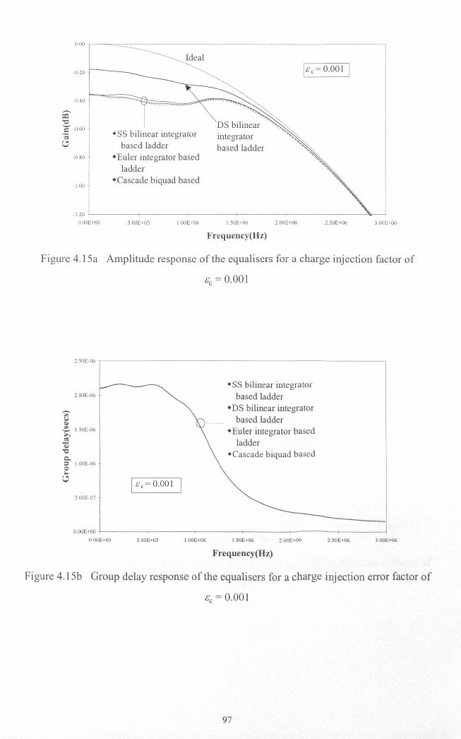
-0.20.1:"----
-0.40.
~"0C -0.60.;C,!)
-0.80
-1.00
+SS bilinear integratorbased ladder
+Euler integrator basedladder
+Cascade biquad based
integratorbased ladder
-1.20 .._----+------+--------if--------i---------if---- ---J
O.OOE+OO 5.00E+05 1.50E+06 2.50E+06 3.00E+06
Figure 4.1Sa Amplitude response of the equalisers for a charge injection factor of
Gc = 0.001
2.00E+061.00E+06
Frequency(Hz)
2.50E-06 -,------------------------------,
'<i;'~<II~ 1.50E-06...,~~"0Q..::s 1.00E-06oloo
C,!)
2.00E-06
5.00E-07
+SS bilinear integratorbased ladder
• DS bilinear integratorbased ladder
• Euler integrator basedladder
• Cascade biquad based
O.ooE+OO +-----+-------+-----+------+-----+-----1O.OOE+OO
18c=0.001
3.00E+06
Figure 4.lSb Group delay response of the equalisers for a charge injection error factor of
e, = 0.001
5.00E+05 2.00E+06 2.50E+061.00E+06 1.508+06
Frequency(Hz)
97

0.00 ,-----=_-=-.:::::::::::::::----------------
·2.50
Ideal·0.50
·1.00
/~~~~~~~~
II".'//,
/1.-,I.-,/.'It
Jt
""integrator based //,I
. based ladder * /'~ ---I-----:__y Euler integrator-,~-=--- based ladder
DS bilinear integratorbased ladder
I·1.50
$'"0-= ·2.00.;C-' SS bilinear
Cascadebiquad
·3.00
-3.50
·4.00 +-----+-----+------+------+------+-------1O.OOE+OO 5.00E+05 1.00E+06 L50E+06 2.00E+06 2.50E+06 300E+06
Frequency(Hz)
Figure 4.l6a Amplitude response of the equalisers for a charge injection factor of
Be = 0.01
2.50E-06,-------------------------------,
S.00E-07
2.00E·06·SS bilinear integrator
based ladder• DS bilinear integrator
based ladder• Euler integrator based
ladder+Cascade biquad based
---Cl>
~~ 1.50E-06~c<:I"ai"0C.= l.OOE-06ol-e.!)
O.OOE+OO-1-----+--------1------+-----+-----+------1O.OOE+oO S.OOE+OS 1.00E+06 1.50E+06 2,OOE+06 2,SOE+06 3,00E+06
Frequency(Hz)
Figure 4.l6b Group delay response of the equalisers for a charge injection error factor of
Be = 0.01
98

=- -10.00"0'-'I::.;e -IS.OO
-. /-- .:- Euler mtegrator
based ladder
-S.oo - DS bilinear integratorbased ladder
• l....'..I~.:·
/1.-{.,}
/ICascade biquad ;,lJI
based 11. ~)'" /~A /Y SS bilinear integrator,'. I . '<...._/ "4-~'--
. /;' '. I.... based ladder'. '-20.00
-25.00+-----+------t-------<f-------t------t-------1O.OOE+OO 5.00E+OS 1.50E+06 2.S0E+062.00E+061.00E+06
Frequency(Hz)3.00E+06
Figure 4.17a Amplitude response of the equalisers for a charge injection factor of
se = 0.05
3S0E-06,.-------------------------------,
300E-06
Cascade biquad based
-~ :". +DS bilinear integrator based ladder;' ". +Ideal ,,,
/'\ •.... f~' .~ Euler integrator based ladder
,\03J ../.' ~ ,.,.'
,-.. 2.S0E-06
'"y~'"'-'>. 2.00E-06~~"0c.. 1.50E-06:se-Co-' 1.00E-06
SS bilinear integratorbased ladder
S.00E-07 I Bc= 0.05
O.OOE+OO-l-----+-------i-----+-----+------+------lO.OOE+OO S.OOE+OS 1.00E+06 1.50E+06 2.00E+06 2.50E+06
Frequency(Hz)3.00E+06
Figure 4.17b Group delay response of the equalisers for a charge injection error factor of
se = 0.05
99

800 ,---------------------------------------------------------,
$' 700"0 --<>- SS-Bilinear integrator ladder'-'e 600 -0-- DS-Bilinear integrator ladderaJ -6- Euler integrator ladder.= 500co= -M-- Cascade biquadell
2l 400co=.ctil
~ 300-c..<l.l.-= 200-'0til.c< 100o~~~==~------~0.001 0.01
Charge injection error EC
0.1
Figure 4.1Sa Relationship between the cumulative passband gain error and charge
inj ection erroreBc)
1.20E-OS ,--------------------------------------------------------,
~tila:: 1.ODE-OStil'-'J...eJ...t 8.00E-06...,co=~"0 6.00E-06c..=eloo
;: 4.00E-U6
=otil.c 2.00E-06-e
--0--- SS-Bilinear integrator ladder-0-- DS-Bilinear integrator ladder-6- Euler integrator ladder-- Cascade biquad
O.OOE+OO ._-- ...... ======:;;;:;;;~;;;;;;;;;;;;;;;~~========------------------l0.001 0.01
Charge injection error EC
0.1
Figure 4.1Sb Relationship between the cumulative passband group delay error and charge
inj ection erroreBc)
100

Settling errors originate from incomplete charging of the memory gate-source capacitor in
the duration of the sampling phase. This results in a non-linear output error current which
introduces distortion to the circuit. For simplicity, we can ignore the non-linearities. The
effect of a linear, small signal settling error e; on the amplitude and group delay responses
of the equalisers are shown in Figs. 4.19~ 4.21. For the same settling time constant, the
responses of the DS-bilinear integrator based ladder are minimally affected due to a
doubling of available settling time resulting from halving the clock frequency. Both the
Euler and SS-bilinear integrator based ladders suffer peaking of the amplitude response at
the cutoff frequency of IMHz. The passband gain of the cascade biquad based equaliser is
minimally affected in comparison. The group delay responses of all the designs are
generally robust to settling errors.
0.20 -,----------------:-:-:-: -------,SS bilinear integrator based ladder
0.00 --_ __,,-=--=--------__ . __·--1. Euler integrator based ladder, ~~l"'-..;::: -,
-0.20
=-"CC -0.40.;c
-0.60 -
-O.SO
+DS bilinearintegrator based ladder+Ideal
18s = 0.1%
-1.00 +------+-----+------+----f-----+-'-.''I.-----lO.OOE+OO S.OOE+OS 1.50E+061.00E+06 2.00E+06 2.S0E+06 3.00E+06
Frequency(Hz)
Figure 4.19a Amplitude response of the equalisers for settling error of Cs = 0.1%
101

2.50E-06 -,--------------------------------,
2.00E-06
-'"ColQj~ 1.50E-06->.~~'Cc..= 1.00E-06elooe
5.00E-07 -
+SS bilinear integratorbased ladder
+DS bilinear integratorbased ladder
+Euler integrator basedladder
-Cascade biquad based
I Cs = 0.1%
O.OOE+OO+-----+--------+------+------+------+-------1O.OOE+OO 5.00E+05 1.00E+06 1.50E+06 2.00E+06 3.00E+062.50E+06
Frequency(Hz)
Figure 4.19b Group delay response of the equalisers for settling error of Cs = 0.1%
DAD -r------------------------------..,
0.20
-= -0.20'C'-'C.;~ -040
-0.60
-0.80
,.... ,,.__Euler integrator based ladder" ,
.... SS bilinear integrator based ladder~\ '\ ..\ '\'\'.v-.
"\ I c,= 0,5%
+DS bilinearintegrator basedladder+Ideal
biquad based-1.00 -I- -+- -+- -+- -+-__ _C>'<-~.;,...----l
O.OOE+OO 5.00E+05 1.00E+06 1.50E+06 3.00E+062.50E+062.00E+06
Frequency(Hz)
Figure 4.20a Amplitude response of the equalisers for settling error of Cs = 0.5%
102

2.50E-06 r--------------------------------,
2.00E-06
+SS bilinear integratorbased ladder
+DS bilinear integratorbased ladder
+Euler integrator basedladder
+Cascade biquad based
-Cl>Y~~ 1.50E-06~e<l~"0c..:s 1.00E-06Q1.0c
5.00E-0? 1£,=°_5% 1
5.00E+05 2.50E+06 3.OOE+06
O.OOE+OO i--------i-----+-----+------I------t---------'O.OOE+OO 1.50E+06 2.00E+061.00E+06
Frequency(Hz)
Figure 420b Group delay response of the equalisers for settling error of e,= 0_5%
0.60 ::----\~Euler integrator based ladder
"'\,:~ b;jlinear integrator based ladder
-.-\, I £ s = 1% ]
0.40
0.20
-0.40
-0.60+rdeal
-0.80
-1.00 +------+-----+- +- ~~--!..-~"_--____I
O.OOE+OO 5.00E+OS 2.00E+06 2.S0E+06I.00E+06 I SOE+06
Frequency(Hz)
3.00E+06
Figure 4_21 a Amplitude response of the equalisers for settling error of Cs = 1%
103

2.50E-06
1&5=1%5.00E-07
2.00E-06
+SS bilinear integratorbased ladder
+DS bilinear integratorbased ladder,-_
'"....Q,j
~ 1.50E-06->.co=~"CQ.= 1.00E-06e..c
+Euler integrator basedladderI
\.; +Cascade biquad based.~...,.~
O.OOE+OO-1------+-----+-----+------+-----+------1O.OOE+OO 5.00E+05 1.00E+06 1.50E+06 2.00£+06 2.50E+06 3.00E+06
Frequency(Hz)
Figure 4.21 b Group delay response of the equalisers for settling errorof Gs = 1%
12,-------------------------------,
-<>- SS-Bilinear integrator ladder-0- DS-Bilinear integrator ladder-4- Euler integrator ladder........Cascade biquad
0.1 0.2 0.3 0.4 0.5 0.6 0.7 0.8 0.9
Settling error £s(%)
Figure 4.22a Relationship between the cumulative passband gain errorand settling
error(Gs)
104

160E-06 -,------------------------------,
~ 1.40E-06
"'"Q,l
'"'i:" 1.20E-06o~~~ 1.00E-06
..:~'1:1 800E-07C.=e~ 6.00E-07~Q,l-.E 400E-07o'".c< 200E-07
--- SS-Bilinear integrator ladder
--0-- DS-Bilinear integrator ladder
---<r-- Euler integrator ladder
--- Cascade biquad
O.OOE+OO -l-----O---.,..--.....,..--.,..----O---.,..--.....,..~=9====F==_$o 0.1 0.6 0.90.7 0.80.3 0.4 0.50.2
Settling error ES(%)
Figure 4.22b Relationship between the cumulative passband group delay error and settling
error(ss)
The plots of cumulative passband gain error and group delay error are shown in Figs. 4.22a
and 4.22b respectively. Not considering the DS-bilinear integrator based ladder design, it is
evident that the cascade biquad based design has the best gain and group delay response
while the worst affected is the Euler integrator based ladder design.
For a final comparison, noise simulations were performed using a unit drain-referred noise
current of 1nA/ Jfu. The noise currents generated by the intemal coefficient transistors of
the filter were scaled in proportion to the root of the respective transconductances. The
simulated noise spectral densities for an arbitrary, fixed noise-bandwidth at a temperature
of T=3000K are shown in Fig. 4.23. Both the SS-bilinear and DS-bilinear integrator based
ladder designs have the highest noise levels in the passband, while the cascade biquad
based design has the lowest noise level.
105

-140 -r--------------------------------,
'N'-142:e'-'-:... -1440'"'"...._$-146"0'-';... -148
a.;;; -150=~"0 -152-eu:..."t -154 -~e,'" -156 -~'"·0Z -158
.',:' Euler integrator.:....- based ladder
Single sampling bilinearintegrator based ladder
-160 j__------t-------+-------+--------t--------1O.OOE+OO 5.00E+05 1.50E+06 2.50E+061.00E+06 2.00E+06
Frequency(Hz)
Figure 4.23 Simulated noise spectral densities for an arbitrary, fixed noise-bandwidth and
a unit reference noise current of InAJ .Jlli
4.4 CONCLUSIONS
Procedures for deriving bilinear integrator based SI allpass equalisers, based on describing
the aUpass function as the sum of a constant and a ladder realisable term, have been
presented. The design can proceed either in the s-domain or directly in the z-domain when
a passive prototype is first synthesised using the respective continued-fraction expansions.
Thereafter, standard matrix methods are used to simulate the allpass structure, The reasons
for implementing the allpass filter using bilinear type integrators are twofold. Firstly,
bilinear integrators do not suffer from excess phase and directly implement the bilinear-
transform. Secondly, bilinear integrator based equalisers are structurally different from
Euler integrator based equalisers, and their sensitivity and non-ideal characteristics merit
investigation. Itwas also shown that the magnitude of the bilinear equaliser is always equal
to I regardless of the deviation in the elements of the reactive ladder section. Generally, it
can be summarised that the best amplitude and group delay sensitivities are shown by the
bilinear integrator based designs and the cascade biquad design respectively, while the
Euler integrator based design fared poorly. For finite conductance ratio errors, the design
106

with the worst affected gain and group delay response is the SS bilinear integrator based
equaliser, while the group delay of the cascade biquad design is least affected. For small
signal signal dependent charge injection error, the best design appears to be the DS-bilinear
integrator based ladder, with both gain and group delay responses of the Euler integrator
based ladder design being the worst affected. For settling errors, the gain response of both
the Euler integrator based ladder and the SS-bilinear integrator based designs perform
worse than the cascade biquad design. The group delay response of all the designs are
robust to the range of settling errors, but the Euler integrator based ladder fared marginally
worse. For noise performance, the bilinear integrator based ladder designs are significantly
worse than the cascade hiquad and Euler integrator based ladder designs.
REFERENCES
[1] L. Gazsi: 'Explicit formulas for lattice wave digital filters' , IEEE Trans. eAS-32, (1),
pp.68-88, 1985.
[2] R. K. Laker, A. Ganesan and P. E. Fleischer: 'Design and implementation of cascaded
switched-capacitor delay equalizers' , IEEE Trans. eAS-32, (7), pp. 700-711, 1985.
[3] B. Nowrouzian: 'Minimal multiplier realisation of bilinear-LDI digital allpass
networks' ,IEE Proc. Pt. G, Vol. 136, (3), pp. 114-117,1989.
[4] B. Nowrouzian: 'A new synthesis technique for the exact design of switched-capacitor
LDI allpass networks', Proc. IEEE ISeAS, New Orleans, USA, May 1990, pp. 2185-2188.
[5] B. Nowrouzian and L. T. Bruton: 'Novel approach to exact design of digital LDI
allpass networks', Electron. Lett., vol. 25, (22), pp. 1482-1484, 1989.
[6] P. Li and J. I. Sewell: 'Active and digital ladder-based allpass filters', Proc. lEE Pt. G,
Vol. 137, (6), pp. 439-445, 1990.
[7] Y.Lu: 'Modem VLSI analogue filter design: methodology and software development',
PhD Thesis, Department of Electronics and Electrical Engineering, University of Glasgow,
1995.
[8] J. B. Hughes and K. W. Moulding: 'Switched-current double sampling bilinear z-
transform filter technique', Procs. IEEE ISeAS, London, UK, May 1994, pp. 293-296,
1994.
107

[9] J. Szczupak, S. K. Mitra and E. I. Jury: 'Some new results on discrete system stability',
IEEE Trans. on Acoustics, Speech, and Signal Processing, vol. 25, (1), pp. 101-102, 1977.
[10] A.EJ. Ng and J.1. Sewell: 'Feasible designs for high order switched-current filters',
Proc. IEE Circuits, Devices and Systems, vo1.l45, (5), pp.297-305, 1998.
[11] R. D. Strum and E. K. Donald: 'Contemporary Linear Systems Using Matlab', PWS
Publishing Company, Boston, 1994.
[12] P. Li: 'Theory and methodology of integrated ladder filter design', PhD Thesis,
Department of Electronics and Electrical Engineering, University of Glasgow, 1990.
[13] C. Toumazou, J.B. Hughes and N.C. Battersby: 'Switched-currents: An analogue
technique for digital technology', IEE Circuits and Systems Series 5, Peter Peregrinus,
London, 1993.
108

CHAPTERS:
LADDER DERIVED SWITCHED-CURRENT DECIMATORS AND
INTERPOLATORS
5.1 INTRODUCTION
5.2 DESIGN PROCEDURE USING MULTIRATE TRANSFORMATIONS
5.3 DECIMATOR STRUCTURES FOR REALISING THE MUL TIRA TE
TRANSFER FUNCTION
5.3.1 Direct Form-II(DFII) Decimator Architecture
5.3.2 FIR-IIR Cascade(FIC) Decimator Architecture
5.3.3 Multiple Feed-In(MFI) Decimator Architecture
5.4 INTERPOLATOR STRUCTURES BY DIRECT TRANSPOSITION
5.5 CIRCUIT SENSITIVITIES AND IMPLEMENTATION ISSUES
5.5.1 Sensitivities
5.5.2 Noise
5.5.3 Implementation Issues
5.6 CONCLUSIONS
REFERENCES
109

5.1 INTRODUCTION
Decimators and interpolators are the basic building blocks used in multirate signal
processing[ 1]. They effect changes in sampling rates and play important roles in many
functions ranging from relaxing the specification of continuous time anti-aliasing(AAF),
anti-imaging filters(AIF)[2] to realising of narrowband bandpass filters[3]. Switched-
current systems[4] are sampled-data in nature and thus also require the bandlimiting of
signals to prevent destructive aliasing. A high sampling rate relaxes the specifications of
the continuous-time input AAF and output AIF but may pose problems of high component
value spreads, high sensitivities to component variations and restricts time available for
settling of system cells. A low sampling rate, while alleviating some of these problems,
demands high order AAF and AIFs. These conflicting requirements are most conveniently
reconciled by the use of decimators and interpolators[5].
SI decimators and interpolators of both FIR and HR types have been previously
proposed[6,7]. These were implemented with polyphase branches and delay blocks that
permit operation at the lower sampling rate Fs, thus maximising the time available for
settling. FIR structures are important for their linear phase, constant group delay
characteristics. However, FIR decimators are generally less selective, unless long impulse
response lengths are used[7]. SI HR structures have been obtained by applying the
multirate-transform[l] to a prototype z transfer function and implemented as direct-form
structures[6]. Although able to realise highly selective functions more efficiently, direct
form structures are known to be more sensitive than doubly terminated ladders. In [8], SI
biquad decimators and interpolators were used in the design of narrowband bandpass filters.
This is not an optimum solution as settling times of the prototype filters are determined by
the higher sampling frequencies and biquads are also known to be quite sensitive to
component variations.
A switched-capacitor decimator was recently proposed[9] which combined low-sensitivity
ladder structures with polyphase input branches. The method was based on the state-space
multirate-transformation of an all-pole LDI ladder filter operating at the higher frequency
MFs to one that operates at the lower frequency Fs. The approximate-LDI
transformation[2] introduces distortion to the passband characteristic which deteriorates
110

with decreasing Fs/fo ratio, whereas the exact-LDI transformation does not. Further, all-
pole responses lack the selectivity of elliptic responses.
In this chapter, switched-current HR decimators and interpolators are proposed, which are
based on the above procedure, but extended to bilinear-transformed, elliptic ladder
structures, The use of bilinear-transformation ensures exactness of response and increases
selectivity by compression of the frequency axis. Highly selective elliptic type responses
with finite-transmission zeros can also be realised. In addition, the low passband sensitivity
of doubly-terminated ladders is preserved and settling time is maximised by operation at
the lower sampling frequency Fs. Two types of decimator architectures which will realise
the multirate transfer function, FIR-HR Cascade(FIC) and Multiple Feed-In(MFI), are
proposed and the steps for deriving them detailed. Applying direct transposition, it is
shown how the interpolator structures can be obtained without the need for redesign. These
are illustrated using an example of a 3rd order elliptic lowpass prototype for a
downsampling and upsampling ratio ofM=L=2 respectively. The remainder of this chapter
deals with sensitivity of these circuits and it is shown that the absence of tight coupling in
the IFC structure results in lower sensitivity in the stopband.
5.2 DESIGN PROCEDURE USING MULTIRATE TRANSFORMATIONS
The basic purpose of a decimator is to reduce the incoming sampling rate at MFs to Fs at
the output as shown in Fig. 5.1. Conceptually, the output signal is formed by discarding
every M'th sample. The frequency responses and signal spectra involved in a decimating
operation of M=2 are shown in Fig. 5.2. The continuous-time anti-aliasing filter preceding
the decimator can be of low order because the higher input sampling rate(MFs) of the
decimator means the images of the input signal spectrum will be spaced further apart.
To prevent aliasing at the decimator output, the input baseband spectrum has to be band-
limited to less than half the output sampling rate, Fs/2. Therefore, even though the
prototype filter within the decimator can have any arbitrary amplitude response, it has to
reject spectral content beyond Fs/2. However, there are exceptions in multistage designs
when some aliasing is tolerated, provided it falls within the filter transition band[l]. The
111

output spectrum of the decimator is shown by a solid trace in the lower half of Fig. 5.2. An
un-bandlimited input signal will result in aliasing as indicated by the dotted lines.
MFs
4
riTna
; ITII..."t~ j+-lIMFs
Fs
Figure 5.1 Symbolic representation of a decimator and its time domain input output
signals
Input continuous-time Decimatoranti-aliasing filter frequency_:-::-: ::-,-t,-O ------~ response ~, ,
1-----..... ,,~_ ' "Input \ ............ ' \baseband " ............ " '.~------r-~----~~~--+-------.--------r~~---r+f
3FsFs/2 Fs 3Fs12 2Fs 5Fs/2
Output Aliasingspectrum~
IBaseb6.Fs/2
Images Aliasing/ "..Jk.Fs 3Fs12
Images
/~.>G.
i • f3Fs
i
2Fs 5Fs/2
Figure 5.2 Frequency domain representation of decimation by M=2
112

function by using the equality[ 1]
A first-order discrete time transfer function can be transformed into a multi rate transfer
M-I kI (a z" )k=O
Original system M=2
(5.1 )
Figure 5.3 Poles and zeros in the z-plane for a 1st order multirate transformed system for
M=2 and M=3 respectively
The relationship in (5.1) states that the original system(LHS) operates at a single high
sampling rate of MFs while the equivalent transformed system(RHS) has a denominator
that operates at the low sampling rate of Fs. In addition, there are now M number of poles
and a numerator term that introduces M-I number of zeros. However, the different transfer
functions are nominally equal due to the pole-zero cancellations shown in Fig. 5.3.
This equivalence can be extended to transform matrix polynomials described in state-space
formulation[9] by re-writing (5.1) as
(5.2)
The state-space transfer function of a z-domain ladder structure operating at the higher
sampling frequency MFs can be expressed[8] in terms of I-Az-1• Using eqn.(5.2), the
transfer function of an approximate-LDI se filter was transformed from single-rate to
multirate, with the denominator represented by the same recursive ladder structure and the
numerator by an FIR polyphase network[9]. The entire structure operates at the lower
sampling frequency Fs. This method can also be used to transform bilinear-LDI type
filters.
113

The response of bilinear-transformed structures are exact and typically have a zero at half
the clock frequency. This zero is usually realised by a A=l +Z-I factor or a bilinear
integrator stage at either the input or output of a bilinear-LDI[lO] filter. Also, elliptic
responses contain finite transmission zeros which are realised by cross-coupling feed-
through branches, i.e. -X41l and -Xs).l as shown in Fig. 5.4 for the signal flowgraph(SFG)
of a 3rd order Right- LU[ 10] lowpass filter.
Figure 5.4 Signal- flowgraph of prototype filter
The differences between this bilinear-transformed SFG and that of a typical approximate-
LDI transformed, all-pole one, are the presence of feed-through branches and the A= (1+z
I) term. A first order bilinear transfer-function has a numerator term of (1+Z-I). This can be
multi rate-transformed using the equivalence
I-M-z= 2--M-_1--L z-k
k=O
(5.3)
The system of equations describing the SFG in Fig. 1 are written as:
(5.4)
or in compact form,
(A-z-'B)V(z)=C(l +Z-I)Vin(Z) (5.5)
114

The output equation is given simply by
Yout (z) = [0 0 1][~~~:~l= DV(z)Y3(z)
To perform the multirate transformations, multiply both sides of (5.5) by A-I to give
(I-z-I A-IB)V(z)=A-IC(1 +z-I)yio(z)
Applying (5.2) to the left hand side and (5.3) to the right hand side of(5.7) yields
[I - (A -IB)M z-M ]V(Z) = X(z)Yin (z)
where
(5.6)
(5.7)
(5.8)
(5.8a)
Substituting (5.6) into (5.8) yields the multirate transfer function.
Yout (z) = D[ I _ (A -IB)M z-M r X(z)Yin (z)
The denominator terms have the form Z-OM,where M=decimation factor; n={O, 1,2, .. N};
(5.9)
N=system order. Thus, the recursive ladder structure operates at the lower sampling
frequency Fs, which translates through to increased time for the memory cells to settle.
5.3 DECIMATOR STRUCTURES FOR REALISING THE MULTlRATE
TRANSFER FUNCTION
Table 5.1 Transistor ratios of the reference elliptic lowpass filter
X9 3.l96775e-Ol
x, 4.576771e-Ol
XL 4.576771e-Ol
XI2 3.611495e-Ol
X4 1.486165e-Ol
x, 2.386774e-Ol
X6 7.560506e-Ol
X7 9.581267e-Ol
x, 4.051205e-Ol
Transistor spread: 6.73
115
Consider the example of a 3rd order Right-LU[IO] elliptic lowpass filter operating at the
higher sampling frequency MFs with M=2. The filter transistor ratios corresponding to the
SFG of Fig. 5.4 are listed in Table 5.1. Substituting these values into (5.4)-(5.6) to form the
respective matrices and applying (5.9) results in the numerical multirate transfer function
6Iakz-k
H(z) = _ -,;:-=-,,-0 --
I b2kZ-2k
k=Owhere the coefficients are listed in Table 5.2.
(5.10)
Table 5.2 Coefficients of the numerical transfer function
<10=0.191961
al = 0.504075
a2= 0.669239
a3= 0.716499
a, = 0.631172
as = 0.360399
a, = 0.088602
bo=4.681974
b2= -3.688141
b, = 3.167880
b6=-1.0
Next, a decimator architecture has to be determined which will realise (5.10) while
preservmg low passband sensitivity and allowing operation at the lower sampling
frequency. Two SI decimator architectures, the FIR-HR Cascade(FIC) and the Multiple
Feed-In(MFI) are proposed. These will be compared to the Direct Form-H(DFII)[6]
decimator structure.
5.3.1 Direct Form-II(DFII) Decimator Architecture
This is the most straightforward method, where a prototype z-transfer function given by
(5.11)
with a unit delay of IIMFs and D = N-l, can be transformed[I,6] into a multirate transfer
function expressed as
116

I(Ian.m)(zMfnH(z) = n~O m~~l
1+ Ibn(zMfnn~l
(5.12)
The imler sum of the numerator can be formed by connecting related sets of coefficient
branches to an input commutator operating at MFs. The outer sum is then formed by
feeding each set via the appropriate block delays to form a polyphase FIR network as
shown in Fig. 5.5. The denominator is realised as a recursive Direct Form-II(DFII)
network with feedback branches.
ao Fslin
1a) -0 lout
-2a2 z
b2a3
-2a4 z
b4as
-2a6 z b,
Figure 5.5 Signal-flowgraph of the Direct Form-II(DFII) decimator
The switched-current implementation of the DFII decimator is shown in simplified form in
Fig. 5.6. The coefficients in Table 5.2 are directly implemented by the transistor ratios in
the circuit.
t2scaled individual VDDbias currents ~connected tothe drain of all .. kIBiastransistors respectively
lout
Figure 5.6 Simplified switched-current Direct Form-II(DFII) decimator schematic
117

5.3.2 FIR-HR Cascade(FIC) Decimator Architecture
This is the first of the two proposed structures, where the numerator term of (5.10) is
realised using an FIR section, which is cascaded with a recursive ladder structure that
realises the denominator term. For a decimating factor ofM=2, the input has to be sampled
twice and the output sampled once. To this end, the FIR part can be polyphase
decomposed[6,7] to obtain a structure that contains Z-2 delay blocks and a two-input
commutator as shown in the lower part of Fig. 5.7. The use of a single commutator allows
many input transistor gates to be tied together. This minimises distortion due to
asymmetric contribution of clock-feedthrough and charge injection by summing of the gate-
source capacitances. Furthermore, as the FIR section is a separate network, scaling can
easily be performed to make the sum of input capacitances of all polyphase networks equal
in value. This causes the charge injection errors to behave approximately as a non-critical
offset[7]. The structure of the doubly-terminated ladder is retained to realise the
denominator while preserving low passband sensitivity. Thus, the individual branches
within the polyphase network and the ladder structure both operate at the lower sampling
frequency Fs, which allows more time for the memory cells to settle.
MFs
Figure 5.7 Signal-flowgraph ofFIR-IIR Cascade(FIC) decimator
118

There is no loss in generality by making the simplifying assumptions X6=X7=XS=X9=XC'
XS=XL and X5=0, then, inspection of the SFG in Fig. 5.7 gives
1VI = - -2 [x,VI + Xc V2 + X(z)Vin]- X4 V3
1-z
V2 = 1 -2 [z-2XC VI + z-2XC V3]1-z
1V3 = - -2 [XCV2 +XL V3]
l-z
Solving (5.13) for the symbolic transfer function and comparing terms with the numerical
transfer function (5.10) results in the set of equations
(XC2XIO) = <to(XC
2XIl) = a,
(Xc2XI2) = a2
(XC2XI3) = a3
(XC2XI4) = a,
(Xc2XI5) = a5
(XC2XI6) = a,
(1+Xs)2 = bo
h X() X X -I X -2 X -3 X -4 X -5 X -6were z = 10+ lIZ + 12Z+ 13Z + 14Z+ 15Z+ 16Z .
2 2 2)Xs +(4-2Xc )Xs+3+Xc (X4-2 = -b2
x,2(X4-2)+2Xs+ 3=b4
(5.13)
(5.14a)
(5.14b)
(5.14c)
(5.14d)
(5.14e)
(5.140
(5.14g)
(5.14h)
(5.14i)
(5.l4j)
Table 5.3 Transistor ratios for the FIe decimator
XIO 0.141317 X4 0.410087
XII 0.371088 X5 0.0
XI2 0.492677 X6 1.165493
Xl3 0.527469 X7 1.165493
XI4 0.464653 Xs 1.165493
XI5 0.265317 X9 1.165493
XI6 0.065227 Xs 1.163787
XL 1.163787
Transistor spread: 17.9
119

This yields the transistor ratios for the FIC structure in Table 5.3. The simplified schematic
of the FIC switched-current decimator implemented using second-generation cells[ 4] is
shown in Fig. 5.8. The bias current sources for each transistor have been omitted to
highlight the circuit connections.
scaledindividualbias currentsconnected tothe drain ofall transistorsrespectively
lout
II2Fs.................~
tl II t2 ......I/Fs
Figure 5.8 Simplified switched-current FIR-HR Cascade(FIC) decimator schematic andclock waveforms
5.3.3 Multiple Feed-In(MFI) Decimator Architecture
This type of structure, first proposed[9] for an LDI, all-pole switched capacitor decimator,
feeds the polyphase-decomposed numerator groups directly to each integrator within the
recursive ladder structure as shown by the SFG in Fig. 5.9.
120

-Xs
Figure 5.9 Signal-flowgraph of the Multiple Feed-In(MFI) decimator
By utilising the delays implicit to the recursive structure, the complexity of each polyphase
feed-in group is minimised. This allows the FIR section of the multiple feed-in(MFI)
structure to use only one, instead of three delay blocks required in the FIC structure.
However, the advantage gained is compromised by higher sensitivity, as will be seen in
Section 5.5. The ladder section is identical to that used in the FIC decimator.
With X6=X7=XS=X9=XCand Xs=XL>the equations for the SFG in Fig. 5.9 are given as
1VI = - -2 [x,VI + Xc V2 + X, (z)Vin] - X4 V3
1- Z
V2 = 1 -2 [z-2XCVl +z-2XCV3 +X2(Z)Vin]1- z
1V3 = - -2 [Xc V2 + XLV3 + X3(Z)Vin] - X5VI
l-z
(5.15)
where X,(z)=XIO+X"z-', X2(Z)=X20+X2,Z"and X3(Z)=X30+X3,Z"+ X32Z·2.
The branch coefficients of the MFI decimator are determined by mapping the symbolic
transfer function to the numerical transfer function in (5.10), as given by
(1+Xs)(XCX20-X30)=ao
(1+XS)(XcX2,-X3,)=a,2x, (Xw-X30)-XCX20+XS(X30-X32)+2X30-X32=a2
(5.16a)
(S.16b)
(S.16c)
121

Xc2(XII-X31)-XCX21+XSX31+2X31=a,2x, X3rXsX32+ X30-2X32=-a4
X31=-a5
X32= -a6
(l+Xs)2=boXs2+(4-2Xc2)Xs+3+Xc 2(X4-2)= -b2
x, \X4-2)+2Xs+ 3=b4
(S.16d)
(5.16e)
(5.16f)
(5.16g)
(S.16h)
(5.16i)
(5.16j)
to yield the set of transistor ratios in Table 5.4. The simplified switched-current realisation
of the MFI decimator is shown in Fig. 5.10.
Table 5.4 Transistor ratios for the MFI decimator
XIO 0.885935 X4 0.410087
XII 0.912658 Xs 0.0
X20 -0.602681 X6 1.165493
X21 -0.109344 X7 1.165493
X30 -0.791135 Xg 1.165493
X31 -0.360399 X9 1.165493
X32 -0.088602 Xs 1.163787
XL 1.163787
Transistor spread: 13.2
In the design procedure, the symbolic transfer functions and decimator transistor ratios
were solved using the MAPLE symbolic engine in MathCad. The need to derive the
symbolic transfer function of the structures imposes an upper limit to the filter order or
decimation factor that can be practically designed. This is because the number of symbolic
terms increases rapidly with system order and decimation factor. For systems of order or
decimation factor greater than six, MathCad failed to converge or yield any solutions. This
presents a serious limitation to the design method.
122

-:-
VDD
~ kJR;"
scaled -:-
individualbias currentsconnected to loutthe drain ofall transistorsrespectively
1/2Fs•............... ~
t1 II t2....................................
IlFs
Figure 5.10 Simplified switched-current Multiple Feed-In(MFI) decimator schematic and
clock waveforms
5.4 INTERPOLATOR STRUCTURES BY DIRECT TRANSPOSITION
The basic function of an interpolator is to increase the incoming sampling rate from Fs to
LFs at the output as illustrated in Fig. 5.11 for sampled and held signals. The frequency
domain spectra and responses are shown in Fig. 5.12 for a simple example of L=2. As
before, the incoming signal has to be band limited to Fs/2. Images will be produced which
will repeat at the lower sampling rate of Fs. At the higher output sampling rate of LFs, the
images that are spaced further apart will coincide with one of the images at the lower
sampling frequency. The task of the prototype filter within the interpolator is to remove the
L-l imaged bands at the output. The images at the output thus repeat at the higher rate of
LFs and will be attenuated by the sinc(x) sample-hold effect.
123

Fs
4LFs
r~'H--+j j+-lIFs
r~···.t--+j j+-lILFs
Figure S.11 Symbolic representation of an interpolator and its time domain input output
sampled and held signals
l~:::~a~'/"'''~Fs/2 Fs
i
3Fs/2 2Fs SFs/2i ~ f
3Fs
Interpolator ~i 2frequency ~t~~~~:~response ~>"::":
Fs/2 Fs 3Fs/2 2Fs SFs/2i ~ f
3Fs
1- - - - - - - - - - - - - - _~~:~~t_~a_~:~~-~td(sinc x) effectOutpu~ ----- -- __spectrtunj i r -~ --------;-----------~f
Fs/2 Fs 3Fs/2 2Fs SFs/2 3Fs
Figure 5.12 Frequency domain representation of interpolation by L=2
124

In general, any linear time-invariant(L TI) or time-varying(LTV) network has a dual or a
complementary network that can be obtained by transposition[l]. In the transposition
operation, all LTI branches remain the same except their directions are reversed. Thus,
input summing points become output branching points and vice-versa. In addition, the
input and output roles of the network are interchanged. A decimator is then transposed to
become an interpolator with the same compression and expansion ratio, that is L=M. It
follows then that equation (5.8) can be written with transposed components as
[IT - {(A -18)M r z-M ]V(Z) = DTVin (z) (5.17)
and equation (5.6) can be written as
Vout(z) = X(z)TV(z) (5.18)
Notice that the positions of the input matrix X(z) and output matrix D have been
interchanged as required and now, V(z)=[V3(z) Viz) Vl(Z)]T. Substituting equation (5.17)
into (5.18) yields the interpolator transfer function
Vout (z) = X(z) T[I _ {(A -18)M rz-M ]-1DTYin (Z)
(5.19)
Comparing this with the decimator transfer function in (5.9), it can be seen that apart from
having transposed matrices, the order of multiplication has been reversed.
For the case of the HR-FIR Cascade(IFC) interpolator, the output equation is given by
Vout(z) = X(Z)TV(Z)
= [0 0 X(z)]V(z)
(5.20a)
For the case ofthe Multiple Feed-Out(MFO) interpolator, the output equation is given by
Vout(z) = X(Z)TV(Z)
= [X3(Z) X2(z) Xl (z)]V(z)
(5.20b)
The SFGs for the IFC and MFO interpolators are shown in Figs. 5.13 and 5.14 respectively.
The first and last integrator will now have to perform Forward Euler, Backward Euler
integration as well as accommodate feedthrough signals.
125

MFsXII
Figure 5.l3 Signal flowgraph ofIIR-FIR Cascade(lFC) interpolator
Fs~-+--____':'f------+---::;:.r-O::::--4--0f-o lin
-Xs
XII
Figure 5.14 Signal flowgraph of MUltiple Feed-Out(MFO) interpolator
Since only the direction of the branches has to be reversed, the same coefficients in Table
5.3 and 5.4 relating to the decimators can be used for the interpolators. This greatly
simplifies the task of deriving the complementary interpolators and avoids the need for
126

tedious redesign from scratch. Similarly, the transposed SFG of the DFII[ 6] interpolator is
shown in Fig. 5.15.
I,....
--0I"-. al ,...-2 ,,_,
Z a2b2 V
II"-. a3-2z a4
b4 Vr-, a5-2
b6z a6
2Fs
Figure 5.15 Signal-flowgraph of the Direct Form-II(DFII) interpolator
The simplified schematic for the switched-current interpolators are shown in Figs. 5.16,
5.17 and 5.18. The input to the interpolators has to be sampled and held. The simulated
ideal frequency responses of both the decimators and interpolators are plotted in Fig. 5.19,
and are identical to that of the reference filter.
scaledindividualbias currentsconnected tothe drain of
lout
1/2Fs.................. ~
12 II 1I.....................................
IIFs
Figure 5.16 Simplified switched-current HR-FIR Cascade(IFC) interpolator schematic and
clock waveforms
127

~~2r--_---'l:'p, I VDD
¢kI".scaledindividualbias currentsconnected tothe drain ofall transistorsrespectively
lout
I12Fs.................. ~12 II II
.....................................IIFs
Figure 5.17 Simplified switched-current Multiple Feed-Out(MFO) interpolator schematic
and clock waveforms
scaledindividual $0bias currentsconnected to '" kIBiasthe drain of
lout
1/2Fs.................. ~
12 II II.....................................
l/Fs
Figure 5.18 Simplified switched-current Direct Form-II(DFII) interpolator schematic and
clock waveforms
128

0.00 ,---==~....--------------..,------------,--===--,
-10.00
-20.00
.-~'0-= -30.00..eo:c
-40.00
-50.00 -
.0., .
-DECIMATOR.._... INTERPOLATOR
....
-60.00 +----t----~--r----I__-_.l_I-h--__+--__+--4H--__+--_;j
0.00 0.20 0.40
................. _.:' .~.' .
0.60 1.40 1.60 1.80 2.00
Figure 5.19 Simulated amplitude responses of the decimators and interpolators
0.80 1.00 1.20
Normalised frequency{fIFs)
Though the examples given here are simple, it is straight-forward to extend to higher
decimation or interpolation rates. However, the significant sin(x)/x attenuation in the
passband will require some form of compensation. Further, the responses are not just
limited to elliptic ones. Unconventional responses such as quasi-elliptic, obtained by
passive prototype manipulation[8], can also be accommodated.
5.5 CIRCUIT SENSITIVITIES AND IMPLEMENTATION ISSUES
5.5.1 Sensitivities
The decimator circuits just described, are based on simulating the multirate-transformed
transfer function of a doubly-terminated ladder network. Therefore, if properly designed,
the characteristic low sensitivity in the passband response should be inherited.
129

In the transformation process, the replicated poles centered around Fs are cancelled by the
additional zeros introduced into the numerator of the transfer function as can be seen from
(S.Sa). The multirate transfer function is thus nominally equal to that of the prototype filter.
Therefore, high sensitivity is expected from elements that contribute to the formation of
these zeros, as any deviation from their nominal values will result in only partial
cancellation of the poles.
The magnitude response sensitivities of the SI decimators to deviations in transconductance
coefficients, computed using (3.15), are plotted in Figs. 5.20 together with that of the filter
and a Direct Fonn-II(DFII)[6] IIR decimator for comparison. The low passband
sensitivities have been preserved by the proposed decimator structures and are indeed even
lower than that of the reference filter. The huge peak in the vicinity of OASf/Fs is caused
by the elliptic notch, while those around O.Sf/Fs result from the sensitivity of the pole-zero
cancellation in the stopband. Unlike a conventional filter, a high stopband sensitivity in the
decimator can result in poor stopband attenuation and aliasing leaking through due to
partial cancellation of the poles.
For the FIC decimator, contributions to the passband sensitivity by the FIR elements are
small, as this section is responsible principally for the formation of zeros. Their main
contribution is to the stopband sensitivity, where the zeros cancel the poles. Conversely,
poles are fanned by the recursive ladder structure and are mainly clustered in the passband
region. This distinct contribution of sensitivity by the FIR and IIR sections to the stopband
and passband respectively happens as both sections are separate and cascaded in the FIC
decimator. This can be seen from (S.14a)-(S.14g), where only branches XS and X7, which
lie in the forward path of the recursive ladder, appear in the numerator of the transfer
function as Xc 2• This minimises contribution to sensitivity due to interaction between
elements of both sections.
130

5.00 I-------I------+------+------I----~0.00 0.20 0.40 0.60 0.80
300.00
250.00
,-..- 200.00 ~e-..="CS'--'150.00 C'>..........
'"==-- 100.00 QJrJJ
- 50.00
0.001.00
";' 25.00 --~-..="CS'--'C.... 20.00.:: 1-----....'[jiCQJ
'""CS 15.00CCIl.Q
'"'"CIl~ 10.00
-Filter-- MFI Decimator-a- FIC Decimator-tr- DFII Decimator
Normalised frequency(f/Fs)
Figure 5.20 Sum-sensitivities of decimators with respect to all transconductance elements
With the MFI structure, different groups of polyphase branches feed directly to each
integrator within the ladder network. This closer degree of coupling between the FIR and
HR sections results in more terms within the recursive ladder appearing in the numerator as
seen from (5.l6a)~(5.l6g). Therefore, a significant increase in stopband sensitivities is
observed in Fig. 5.20 for the MFI decimator as expected. Both passband and stopband
sensitivities are relatively higher for the DFII decimator[6]. The frequency responses
resulting from a ±1% deviation in all coefficients are plotted in Figs. 5.21a and 5.21b. The
DFH and MFI decimators exhibit the greatest amount of response deviation in the passband
and stopband respectively while the FIe decimator is minimally affected for both regions.
The sensitivity performance of the interpolators are shown in Fig. 5.22. Low passband
sensitivities are preserved but are marginally higher. The stopband sensitivities are
significantly worse than those for the decimators. Sensitivity is topology dependent, and
the increased sensitivities of the interpolators are therefore caused by the altered topologies
resulting from the direct transposition process.
131

0.20 1--------;========::::::;---------;::;:-----1
0.10... IDEAL~ FIC Decimator-<>- MFI Decimator----.-DFII Decimator=- -0.10 qr-_ _....._
'0'-'~ -0.20
=.....:a -0.30
8-< -0.40
-0.50
-0.60
-0.70 +- --+ --+- !-- -+--\~ _ __J
0.00 0.05 0.15 0.200.10
Normalised frequency(f/Fs)
Figure 5.21 a Effect of ± 1% deviation in all transconductance on the passband of thedecimators
-32.00 ~.------------------------------,
-34.00
=- -38.00
'0'-'~ -40.00
=.....:a -42.00 -
8-< -44.00
-48.00
. .. IDEAL~ FIC Decimator-<>- MPI Decimator----.-DFII Decimator-46.00 -
-50.00 -\---=-4--1:1-=--+-------+-------+-------1--------10.40 0.50 0.70 0.800.60
Normalised frequency(f/Fs)
Figure 5.21 b Effect of ±1% deviation in all transconductance on the stopband of thedecimators
132
0.90

30.00.----------+-t--,-------HH-----------------,-
10.00b~~~~~~;;~~~----==:=====;:::::====:l0.00 0.20 0.40 0.60 0.80
1000.00
900.00
SOO.OO
- 700.00 -.~Q"-
- 600.00 ="C'-'500.00 C:~....400.00
._<I}=Q)
300.00 00
- 200.00
100.00
0.00
1.00
"C 18.00
=~~ 16.00<I}<I}~~ 14.00
-Filter-<>- MFO Interpolator-- IFC Interpolator----DFII Interpolator
2S.00
Rightscale--~
12.00
Normalised frequeocy(f/Fs)
Figure 5.22 Sum-sensitivities of interpolators with respect to all transconductanceelements
5.5.2 Noise
For noise simulations, a unit drain-referred noise current of lnAl.JHz. was used and the
noise generators associated with the branch coefficients were scaled in proportion to the
root of the respective transconductances. Considering a fixed arbitrary noise bandwidth,
noise foldback effects and a temperature ofT=300oK, the resulting spectral densities for the
decimators and interpolators are plotted in Figs. 5.23 and 5.24 respectively. The MFI
decimator has a marginally lower noise level in the passband in comparison, while the DFII
decimator has the highest noise level.
For the interpolators, the DFII structure clearly has the lowest noise level in the passband,
which is comparable to that of the decimators. However, changes in topology to both of the
IFC and MFO interpolators resulting from the direct transposition process also changes the
internal noise transfer functions to the respective outputs. This results in higher noise
levels for the IFC and MFO interpolators since noise is folded back at the same higher
output frequency of 2Fs for all the interpolators.
133

-156.00 -,----.-- ..----------- ,
g -158.00....""0"~..._$' -160.00 !><><>OOO<XXXl()()()<:>OV'-
"0'-';,.... -162.00.......~=~ -164.00
';
""....a:: -166.00-·Q.~Q,j.~ -168.00oZ
-0- FIC Decimator-6- MFI Decimator··x· DFII Decimator
-170.00 I------+------+-------+-------t-----~~O.OOE+OO 5.00E+06 1.00E+07 1.50E+07 2.00E+07 2.50E+07
Frequency(Hz)
Figure 5.23 Simulated decimator noise spectral densities with IO-band foldback effects,
T=300oK and a unit drain-referred noise current of InN JH.i,
-1.50E+02 -.r------,-------:--------,--------------,
g....6- -1.55E+02 -t·"lo6t>o!_o!olo!,ololQo.t.o.lo6oloo!~~<Il..._----~"0'-' x;, -1.60E+02c" . xxxx)(X>OO<XI'X,._ ~~= xQ,j ~
i.<M'"" ~!FC Interpolator '1.,.[~ ~<Il _I 70E+02 -6- MFO Interpolator i XXXxQ,j , I
~ .. x···DFII Interpolator I
-1.75E+02 +------+------+------+------1--------1O,OOE+OO 5.00E+06 1.00E+07 1,50E+07 2,OOE+07 2.50E+07
Frequency(Hz)
Figure 5.24 Simulated interpolator noise spectral densities with Iu-band foldback effects,
T=300oK and a unit drain-referred noise current of InA! JH.i,
l34

Table 5.5 Dynamic range scaled transistor ratios of the FIC decimator
XIO 0.141317 X4 0.410087
XII 0.371088 Xs 0.0
Xl2 0.492677 X6 1.958000
X13 0.527469 X7 1.958000
Xl4 0.464653 X8 0.693750
Xl5 0.265317 X9 0.693750
Xl6 0.065227 Xs 1.163787
XL 1.163787
Transistor spread: 30
5.5.3 Implementation Issues
To give a more realistic assessment of circuit implementation, an M=2 FIC decimator and
an L=2 IFC interpolator were simulated in HSPICE using real process models. Dynamic
range scaling[16] was performed to equalise the peak signal modulation of the bias currents
in the different stages. The scaled signal levels of the FIC decimator are shown in Fig. 5.25
and the corresponding transistor ratios are listed in Table 5.5.
Ij
\j~1\\
/:Output level of 3rd integratorI
4.00
2.00
0.00
,-._~"'I:S -2.00'-'==.~C-' -4.00 -
-6.00
-8.00 -
I ··r········~><~·///l/I//I , »>: • .. ·r·---------r- :I I
OUtput level of 1st integrator :
I Output level of ~nd integrator
Commutator output"1 '.. ..
connected to FIRpolyphase tansistors:Even inpuf Odd input
i
5.00E·02 2.00E-OJ
-JO.OO-·~----+-----+------+--- __ +-- -+_~_"___'O.OOE+OO 2.50E-OJ 3.00E-01LOOE·OJ L50E-OJ
Normalised frequeocy(f/Fs)
Figure 5.25 Dynamic range scaled signal levels of the FIC(M=2) decimator
135

The delay circuit that is fed by FIR transistors X12~X16(Fig. 5.8) has to be doubled in size
to sink the summed currents. The memory cells were designed using models from an AMI
double-metal l.Ourn digital CMOS process, and employ the S2I[12] technique with
cascodes and dummy switches added to reduce the output conductance and charge-injection
respectively. The unit memory cell and associated clock waveforms are shown in Fig. 5.26
while its specifications are listed in Table 5.6. As the S2I cell delivers the corrected current
only in its output phase, care has to be taken to ensure direct feedthrough connections are
minimised by rearranging the connections or by introducing a half-delay with a memory
cell. Finally, settle scaling[ 15] of the transistors was performed to ensure the gate area of
the loaded integrator outputs remained unchanged. Fig. 5.27 shows the HSPICE and
SCNAP4[11] simulated frequency responses of the FIC decimator and IFC interpolator.
The respective output responses to a sampled-and-held 100kHz sinusoidal input signal at
50% modulation of the bias current are shown in Figs. 5.28 and 5.29. The decimating and
interpolating actions are clearly evident.
Table 5.6 Specifications of the SI memory cell
Transistors (W/L) in urnBias current, MJ 42/2Bias cascode, MJC 80/1Memory cascode, Mc 30/1Main memory, MJ 50/4Current transfer switches 20/1Sampling switches 3/1Bias current 100_gAVDD(VSS=OV) 3VVBias1 1.5VVBias2 1.2VVCas 1.8V
136

VDD
VBiasl
VBias2 n---+--~
iin ~--_''''_---e--__'
yeas ~--+--~
VSS
\'--------11'"lax h:: ~'f'/::~:¢la rL_j___J¢lb~
¢1 I
Figure 5.26 Cascoded S21memory cell and clock waveforms
1.00
0.80
0.60
--040 ~
S0.20 ]
~"t:l-I----~+------+-----+ 0.00 "t:l
==e'.I~--t" -0.20 ,.Q
r.flr.fle':
-040 P.
-20.00
o
o
.-~S.5 -30.00e':c
Righ scale _.
-40.00
(HSPICE) IFCInterpolator
-0.60
-0.80
Freq uency(Hz)
-60.00 -l-----+----+l-----i-----+--W---+-----+ -1.00O.OOE+OO 1.00E+05 2.00E+05 300E+05 4.00E+05 500E+05 600E+05
Figure 5.27 SCNAP4 and HSPICE simulated frequency response of the M=L=2 FICdecimator and IFC interpolator
137

6.00E-OS ,..-------------------------------,
4.00E-OS
2.00E-OS -.-S....ffi O.OOE+OO~~=U
-2.00E-OS -
-4.00E-OS
100kHz input~- signal current
sampledat2MHz
Decimatoroutput currentsampled at IMHz
-6.00E-OS +---+----+----+----f---___,'-----+----r----+----+--~7.80E-OS 8.00E-OS 8.20E-OS 8.40E-OS 8.60E-OS 8.80E-OS 9.00E-OS 9.20E-OS 9.40E-OS 9.60E-OS 9.80E-OS
Time(Secs.)
Figure 5.28 HSPICE simulated decimator output responses(M=2) for a 100kHz sampled-and-held input sinusoidal signal
6.00E-OS
4.00E-OS
2.00E-05.- -<'-'.... r-=<l) O.OOE+OO --~~=U
-2.00E-OS
--4.00E-OS --
-6.00E-05
7.90E-OS
100kHz input_ -r-n..__ signal current
- - - I'. c- sampled- at IMHz__ r-
__r--n~ r- I L
r--- -
i-t-r-
-- r-r-
i /r- r-r-r- ,
[Interpolator r-
output current r-~U-sampled at - I
! 2MHz I-r-r-
-
t-
t-t-
8.IOE-OS 8.30E-OS 8.S0E-OS 8.70E-OS 8.90E-OS 9.IOE-OS 9.30E-OS 9.S0E-OS 9.70E-OS 9.90E-OS
Time(Secs.)
Figure 5.29 HSPICE simulated interpolator output responses(L==2) for a 100kHz sampled-and-held input sinusoidal signal
138

5.6 CONCLUSIONS
Bilinear-transformed, elliptic switched-current decimators and interpolators based on a
combination of polyphase networks and low sensitivity ladder structures have been
demonstrated with an M=L=2 fold reduction/increase in sampling rate. Settling time for
the memory cells is maximised by the use of polyphase FIR networks, which together with
the prototype filter, operate at the lower sampling rate. Of the two types of proposed
structures, the FIR-HR Cascade(FIC) type requires more delay terms, but is simpler and
possesses superior sensitivity characteristics. The Multiple-Feed-In(MFI) type requires less
delay terms, but suffers from poorer sensitivity characteristics. However, both exhibit
passband sensitivities that are lower than that of the basic filter. The direct transposition
method avoids redesign to obtain the interpolator structures, which share similar sensitivity
characteristics, apart from the stopband region. Noise performance of the decimators are
comparable. In comparison, the IFC and MFO interpolator structures obtained by direct
transposition resulted in marginally higher noise levels. One serious drawback of this state-
space multirate transform design method is the need to derive the symbolic transfer
function of the structures. The rapid increase in the number of symbolic terms with filter
order and decimation/interpolation factor effectively imposes a limit on the achievable
design. Nevertheless, this is mitigated by the other favourable attributes mentioned, which
together with high selectivity and exactness of response, make the proposed switched-
current decimators and interpolators suitable for high frequency filtering applications.
REFERENCES
[1] R.Crochiere and L.Rabiner, "Multirate digital signal processing", (Englewood Cliffs,
NJ: Prentice Hall, 1983).
[2] R.Gregorian and G.C.Temes, "Analog MOS integrated circuits for signal processing",
(Wiley, New York, 1986)
[3] J. E. Franca, "Single-path frequency-translated switched-capacitor system for filtering
and single sideband generation and detection", Proceedings - IEEE International
Symposium on Circuits and Systems, pp. 1625-1628, Kyoto, June 1985.
139

[4] C.Toumazou, lB.Hughes and N.C.Battersby, " Switched-currents: An analogue
technique for digital technology", (Peter Peregrinus Ltd., London, 1993).
[5] R.Gregorian and W.E. Nicholson, "Switched-capacitor decimation and interpolation
circuits", IEEE Trans. CAS, vol. CAS-27(6), pp. 509-514, 1980.
[6] W. Ping and J. E. Franca, "Switched-current multi rate filtering", Proceedings - IEEE
International Symposium on Circuits and Systems, vol. 5, pp. 321-324, London, May 1994.
[7] M. Helfenstein, J. E. Franca and G. S. Moschytz, "Design techniques for hdtv switched-
current decimators", Proceedings - IEEE International Symposium on Circuits and
Systems, vol. 1, pp. 195-198, Atlanta, May 1996.
[8] Y. Lu and J.1. Sewell, "Multirate SC and SI Filter system design by XFILT",
Proceedings - IEEE International Symposium on Circuits and Systems, vol. 3, pp. 2257-
2260, Seattle, April 1995.
[9] P. J. Santos, J. E. Franca and J. A. Martins, "Switched-capacitor decimators combining
low-sensitivity ladder structures with high-speed polyphase networks", IEEE Trans. CAS
II: Analog and Digital Signal Processing, vol. 43, (1), pp. 31-38, 1996.
[10] Y. Lu and J. I. Sewell, "Systematic approach for ladder based switched-current filter
design", Proceedings - IEEE International Symposium on Circuits and Systems, vol. 3, pp.
2253-2256, Seattle, April 1995.
[11] Z.Q. Shang and Ll. Sewell, "SCNAP4 Users' Guide v1.8", Department of Electronics
and Electrical Engineering, University of Glasgow, March 1998.
[12] LB. Hughes and K.W. Moulding, "S21_ a switched-current technique for high-
performance", Electron.Lett., 1993,29, pp.1400-1401
[13] lB. Hughes and K.W. Moulding, "S3I: the seamless S2I switched-current cell",
Proceedings - IEEE International Symposium on Circuits and Systems, pp. 113-116, Hong
Kong, June 1997.
[14] P. Shah and C. Toumazou, "A new high-speed low distortion switched-current cell",
Proceedings - IEEE International Symposium on Circuits and Systems, 1, pp.421-426,
Atlanta, May 1996.
[15] N.C. Battersby, "Switched-current techniques for analogue sampled-data signal
processing," Ph.D. Thesis, Imperial College of Science, Technology and Medicine,
University of London, February 1996.
[16] T.S. Fiez and DJ. Allstot, "CMOS switched-current ladder filters," IEEE J. Solid-
State Circuits, vol.2S, (6), pp.1360-1367, 1990.
140

CHAPTER6:
N-PATH AND PSEUDO-N-PATH CELLS FOR SWITCHED-CURRENT SIGNAL
PROCESSING
6.1 INTRODUCTION
6.2 SWITCHED-CURRENT N-PATH AND PSEUDO-N-PATH CELLS
6.2.1 Switched-Current z~ -z Transform Integrators
A. Forward Euler Integrator
B. Backward Euler Integrator
C. Bilinear Integrator
6.2.2 Switched-Current Pseudo-2-Path z~ _Z2 Transform Integrators
A. Forward Euler Integrator
B. Backward Euler Integrator
C. Bilinear Integrator
D. FIR Section (1_z-2)
6.3 EFFECTS OF NON-IDEAL FACTORS ON PSEUDO-N-PATH
INTEGRA TORS
6.3.1 Finite Output/Input Conductance Ratio Errors
6.3.2 Clock-feedthrough and Charge-injection Errors
6.3.3 Settling Errors
6.4 SWITCHED-CURRENT N-PATH AND PSEUDO-N-PATH LADDER
FILTER DESIGN
6.4.1 Switched-Current N-Path Ladder Design
6.4.2 Switched-Current Pseudo-N-Path Ladder Design
6.4.3 Sensitivity and Non-Ideal Factors
6.5 CIRCUIT IMPLEMENTATION ISSUES
6.5.1 Memory Cell
6.5.2 Common-mode Control
6.5.3 A 6th Order Pseudo-Z-Path SI Bandpass Filter
141

6.6 CONCLUSIONS
REFERENCES
142

6.1 INTRODUCTION
The concept of N-path[l] filtering was originally proposed for continuous time bandpass
applications, and was subsequently extended to digital and switched-capacitor(SC)
filters[2]. It is most commonly employed to derive narrowband bandpass filters[3], which
might otherwise not be practical due to high component spreads and sensitivity. More
importantly, the centre frequency of a discrete time N-path filter is centered at a multiple of
the clock frequency, which provides the necessary frequency stability crucial to narrowband
bandpass filtering. However, various problems plaguing the traditional N-path filter, such
as path mismatches, mirror frequency noise and clock- feedthrough noise[3] have prompted
the development of alternative methods.
The pseudo-N-path concept was proposed by Fettweis and Wupper[4] to overcome the
problem of path mismatch. Instead of having N distinct paths, only one common path
exists through which all signals traverse. Each memory-possessing element has to be
supplemented by a circulating delay line which shifts the different states such that an N-
path filter is realised. Circulating-delay and other variants[3, 5, 6, 7] of pseudo-N-path SC
filters have already been in existence for some time.
N-path filters can be designed using either a lowpass or a highpass reference filter. Fig. 6.1
shows the amplitude response ofN-path filters which use a lowpass prototype to achieve a
Z~ZN transformation. Generally, the Nyquist range is extended from Fs/2 to NFs/2. Each
path filter has to be clocked at Fs in a time-interleaved manner to achieve an effective
sampling rate of NFs. For pseudo-N-path filters, the clock rate has to be NFs, as there is
only a common signal path through which all paths are processed. It is clear from Fig. 6.1
that to utilise the passband centered at Fs, a minimum of N=3 paths are required. Further
disadvantages include the need for bandpass anti-aliasing(AAF) and anti-imaging
filters(AIF) due to the undesired passband at DC, and the presence of clock-feedthrough
noise in the passband for N-path type realisations.
143

ALPF N;I-+: N;2-+: N;3-+:
t1 [~ f
0 Fsl2 Fs 3Fsl2 2Fs
Figure 6.1 Nyquist range ofN-path filter with lowpass prototype response
Figure 6.2 Nyquist range ofN-path filter with highpass prototype response
In comparison, the use of highpass prototype filters with the Z~ZN transformation has the
response shown in Fig. 6.2. Only N=2 paths are required to utilise the passband centered at
Fs/2. Simple lowpass AAFs and AIFs can now be used instead of bandpass ones. More
importantly, the desired passbands are centered at odd multiples of Fs/2, which avoid clock-
feedthrough noise. To obtain the type of response in Fig. 6.2 using only lowpass filters,
the Z~ _ZN transformation can be used[7], which features in the cells proposed here.
Very few papers, if any, have to date been published in the area of N-path or pseudo-N-
path SI circuits. In this chapter, novel SI N-path and pseudo-N-path cells based on the
Forward Euler, Backward Euler and bilinear integrators are proposed. A z-domain lowpass
reference filter can be transformed into a bandpass one by simply replacing the original
integrators with the corresponding proposed cells. The fully-balanced integrators perform
the z~ -z(lowpass to highpass) transformation and the z~ _Z2 (lowpass to bandpass)
transformation, which is based on the circulating-delay principle. The effects of non-
idealities such as finite conductance ratio, settling, clock feedthroughlcharge-injection and
noise on the pseudo-N-path integrators are analysed in detail. Using these cells, the
procedures for designing ladder filters from a z-domain lowpass reference filter are
illustrated with an N-path and a pseudo-N-path 6th order narrowband bandpass ladder filter.
144
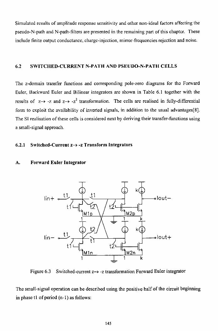
Simulated results of amplitude response sensitivity and other non-ideal factors affecting the
pseudo-N-path and N-path-filters are presented in the remaining part of this chapter. These
include finite output conductance, charge-injection, mirror-frequencies rejection and noise.
6.2 SWITCHED-CURRENT N-PA TH AND PSEUDO-N-PATH CELLS
The z-domain transfer functions and corresponding pole-zero diagrams for the Forward
Euler, Backward Euler and Bilinear integrators are shown in Table 6.1 together with the
results of z---+-z and z---+_Z2 transformation. The cells are realised in fully-differential
form to exploit the availability of inverted signals, in addition to the usual advantages[8].
The SI realisation of these cells is considered next by deriving their transfer-functions using
a small-signal approach.
6.2.1 Switched-Current z---+-z Transform Integrators
A. Forward Euler Integrator
lin+ ~--r---k-- '----.-.---1
t
Figure 6.3 Switched-current z---+-z transformation Forward Euler integrator
The small-signal operation can be described using the positive half of the circuit beginning
in phase tl of period (n-I) as follows:
145

tl(n-I)
iM1p(n-I) = ii/(n-I)-iM2P(n-I)
iout-(n-I) = -iM2p(n-l)
t2(n)
(6.la)
(6.Ib)
iM2p(n)= iM1p(n)
iout-(n)= -iM2p(n)
Substituting memorised current iM1p{n)= iM1p{n-l)and (6.1d), (6.lb) into (6.1c) gives
(6.Ic)
(6.1d)
-iout-(n)= iin\n-I)+ iout-(n-I)
Taking z-transfonns and rearranging yields the transfer function
(6.Ie)
_Z-1
HFE{z)=k 11+ z:
where k=I will be assumed throughout.
(6.1 f)
B. Backward Euler Integrator
The z~ -z transform Backward Euler integrator can be obtained with the same cross-
coupled, differential feedback structure as it shares a common denominator term. However,
the inputs are sampled by memory cells M2p and M2n in phase t2 instead as shown in
Fig.6.4.
I----olout-
I----olout+
Figure 6.4 Switched-current z~ -z transformation Backward Euler integrator
The circuit operation is described as follows:
146

tl(n-l)
iM1p(n-l)= -iM2p(n-l)
iout-(n-l) = -iM2p(n-l)
t2(n)
iM2p(n)= iin\n)+iM1P(n)
(6_2a)
(6.2b)
iout-(n)= -iM2p(n)
Substituting memorised current iM1p(n)= iM1p(n-l) and (6.2d), (6.2b) into (6.2c) gives
- iout-(n)= iin\n)+ iout-(n-l) (6.2e)
(6.2c)
(6.2d)
Taking z-transfonns and rearranging yields the transfer function
(6.2f)
C. Bilinear Integrator
The bilinear integrator can be formed from the same basic structure and is shown in Fig.
6.5. Due to a numerator term of (l-z"], the input will have to be sampled on both phases.
A full period sample-and-hold is therefore required at the input.
lin-
lin+
Figure 6.S Switched-current Z~ -z transformation Bilinear integrator
147

The circuit operation is described as follows:
n(n-I)
iM1p(n-I)= iin\n-l)-iM2p(n-l)
iOl/(n-l) = -iM2p(n-l)
t2(n)
iM2p(n)= iin-(n)+iMIp(n) (6.3c)
iou/en) = -iM2p(n) (6.3d)
Substituting memorised current iM1p(n)= iM1p(n-l), iin-(n)= -iin\n) and (6.3d), (6.3b) into
(6.3c) gives
(6.3a)
(6.3b)
-iout+(n)= -iin+(n)+ii/(n-l)+ iout\n-l)
Taking z-transforms and rearranging yields the transfer function
1-Z-IHBI(Z)= k _I
1+z
(6.3e)
(6.3f)
To verify the correct operation of these circuits, computer simulation was performed using
the switched network simulator SCNAP4[9]. The resulting amplitude responses are shown
in Fig. 6.6 and correspond exactly with responses expected from the respective pole-zero
diagrams in row two of Table 6.1.
50.00 -.,..-------------------------,
40.00
30.00
20.00FORWARD EULER,BACKWARD EULER
-20.00 -
-30.00
-40.00
-50.00 -11--------+--------+- ----1 ---11o 0.25 0.5 0.75
Frequency(f/Fs)
Figure 6.6 Simulated amplitude responses of the z~ -z transformation integrators
148

6.2.2 Switched-Current Pseudo-2-Path Z~ _z'2Transform Integrators
A. Forward Euler Integrator
lin+
lin-
Figure 6.7 Pseudo-2-path switched-current Z~ _Z2 transformation Forward Euler
integrator
The simplified schematic of the fully-differential Z~ -i transform, pseudo-2-path Forward
Euler integrator is shown in Fig. 6.7. Transistors Mlp-M4p and Mln-M4n form a
differential Z-2 delay pair. Two delay cells are required in each path to satisfy the pseudo-2-
path circulating delay principle. The integrating loops can be formed with sign reversal of
the delay terms by cross-coupling the feedback loops as shown. The small signal operation
of the circuit can be described starting at phase tl of period (n-2) as follows:
tUn-2)
iM1p(n-2)= ii/(n-2)-iM4n(n-2)
Since iM4n= -iM4p= iout+/k
iM1p(n-2)= ij/(n-2)- iout+(n-2)/k
t2(n-l)
iM2p(n-l) = -iM1p(n-2)
= -[iin+(n-2)- iout+(n-2)/k]
(6.4a)
(6.4b)
(6.4c)
tUn-I)
iM3p(n-l) = -iM2p(n-l)
= iin+(n-2)-iout+(n-2)/k (6.4d)
149

t2(n)
iM4p(n) = -iM3p(n-l)
= -i. +(n-2)+i "(n-Zj/kIn out (6.4e)
Substituting iM4p = -iout+/kand some rearranging gives
iou/(n)+ iout+(n-2) = ki., +(n-2)
Taking z-transforms yields
iout+(z)(l +z-2)= ki., \z)z-2
From (6.4g), the transfer function is given as
(6.4f)
(6.4g)
(6.4h)
B. Backward Euler Integrator
The Backward Euler integrator is shown in Fig. 6.8. The inputs are sampled at memory
cells M 1P and MIn in phase t2 to established a direct path between the input and output as
required for Backward Euler integration. The cross-coupling reverses the sign of the loop
delay. The circuit operation is described as follows:
lin+~
t---Iout-
I---Iout+
Figure 6.8 Pseudo-2-path switched-current z~ _Z2 transformation Backward Euler
integrator
150

tl(n-2)
iM4pCn-2)= -iM1pCn-2)
Since iM1p= -iout"/k
iM4pCn-2)= iout"Cn-2)/k
t2(n-l)
iM3pCn-l)= -iM4pCn-2)
= -iout"Cn-2)/k
(6.5a)
(6.5b)
C6.5c)
t1(n-l)
iM2p(n-l) = -iM3rCn-l)
= iout"(n-2)1k C6.5d)
t2(n)
iMlnCn)= -iM2p(n-l)+iin"Cn)
= -iout"(n-2)Ik+iin"Cn)
Substituting iM1n= -iout+1k= iout"1kand rearranging gives
iout\n)+ iout+Cn-2)= -kiin"(n)
Taking z-transforrns yields
iout+(z)C1+Z"2)= -kiin"Cz)
From (6.5g), the transfer function is given as
(6.Se)
(6.5f)
(6.5g)
1HBECZ)=-k _1+z2 C6.Sh)
C. Bilinear Integrator
Fig. 6.9 show the schematic of the bilinear integrator. A full period sample-and-hold is
required at the input as it samples on both phases. Note that the cross-coupled connection
reverses the sign of the loop-delay while feedback is now to the middle of the delay line.
This section can be used to realise bilinear-integrator based ladder filters. Similarly, the
operation of the circuit can be described starting from the positive input as follows:
t1 (n-2)
iM1pCn-2)= iin\n-2)
t2(n-2)
iM6p(n-2)= -iout+(n-2)/ k
(6.6a)
(6.6b)
151

iM2p(n-2)= -iM1p(n-2)
tl(n-1)
iM3p(n-l) = -iM2p(n-2)-iM6p(n-2)
t2(n-l)
iM4p(n-l) = -iM3p(n-l)
llinl
(6.6c)
(6.6d)
(6.6e)
(6.6f)
(6.6g)
Substituting in the previously memorised currents and noting that iM6n(n)= -iout-(n)1k=iou/(n)/k gives
iout\n)+ iou/(n-2) = k[iin"(nj-i.,\n-2)]
Taking z-transforms and rearranging yields the bilinear transfer function
1-Z-2HBl(Z)= k -2
l-t z
(6.6h)
(6.6i)
lout+
lout-
Figure 6.9 Pseudo-2-path switched-current z~ _z2transformation Bilinear integrator
D. FIR Section (I-z")
This circuit in Fig. 6.10 is designed to replace the bilinear integrator required at the input of
certain z~ _Z2transformed, bilinear-LDI filters. Cascading the FIR section at the output
instead of having a bilinear integrator at the input avoids overloading the filter with the
peak in response at Fs/4 while simultaneously realising the bilinear zero at Fs/2. Without
152

going through details, the circuit operation can be described as follows: The outputs from
transistor pair M2p and M2n are fed to delay lines realising two unit delays of _z-2. The
outputs from Mlp and MIn are then cross-connected directly to the output which sums to
give the transfer function HFIRCZ) = I-z".
Figure 6.10 FIR output section (1_z-2)for realising the bilinear zero
50.00
40.00
30.00 -FORWARD EULER,BACKW ARD EULER
20.00 -
1,-.~'0 10.00'-'QJ'0= 0.00 -;:::c..e -10.00 --
-<-20.00 -
-30.00
-40.00
-50.000 0.25 0.5 0.75
Frequency(f/Fs)
Figure 6_11 Simulated amplitude responses of the Z--1- _z2transformation pseudo-2-path
integrators
153

To verify the correct operation of these circuits, they were simulated and the resulting
amplitude responses are shown in Fig. 6.11. These responses correspond as expected to
those from the respective pole-zero diagrams in row three of Table 6.1.
Table 6.1 z-domain pole-zero diagrams and transfer functions for the transformed
integrators
z-plane
Original
Forward Euler Backward Euler Bilinear
z-plane
z~ -ztransformation
1/2z -plane
2z~ -ztransformation
1Hsdz)= -k 1 -I-z
-IzHFECZ)=-k 1 -I
+z
1HSECZ)= -k _
1+z I
1HSECZ)= -k--
1+z-21 -2-z
H8ICz)= k -2l+z
154

6.3 EFFECTS OF NON-IDEAL FACTORS ON PSEUDO-N-PATH
INTEGRA TORS
In this section, the effects of non-idealities such as finite output/input conductance
ratio, clock-feedthrough, charge-injection and incomplete settling of memory cells on
the response of the pseudo-2-path integrators are addressed. To varying extents, most
non-ideal factors will cause distortion, with significant contributors being charge-
injection and incomplete settling of memory cells. However, the effort here is focused
mainly on linear, small-signal errors and their effect on the frequency response. Full
transistor level SPICE simulations take excessively long amounts of time to run.
Further, it is only possible to perform time-domain transient simulations of the
switched-networks. Therefore, it is highly desirable to develop simplified models that
are relatively fast, maintain reasonable accuracy, and can be used in direct AC
simulations using the switched-network simulator SCNAP4[9]. Theoretical basics of
the non-ideal phenomena are given and where possible, comparisons are made
between theoretical and simulated results.
VH
iin iout(61 I \ VL I(62 \ I \
Figure 6.12 Basic second-generation switched-current memory cell and clock phases
6.3.1 Finite Output/Input Conductance Ratio Errors
To understand the error mechanisms associated with finite output/input conductance
ratios, consider the operation of the basic second generation SI memory cell of Fig.
6.12. On the sampling phase(~I), transistor MM is diode connected, forcing its drain
155

voltage to be the same as Vgs- When the holding mode is entered( ¢2), the memorised
current is delivered to the load at the output. Any change in the drain voltage during
this phase will produce an error current as a result of two main effects. The first of
these is channel shortening, which gives a drain current of
where A is the channel shortening parameter, and a drain conductance of
t3Ig- dS_1Ids- OV - /l.. ds
ds
(6.7)
The second effect is due to the drain-gate(Miller) overlap capacitance Cdg' which
couples voltage variations at the drain into the memory capacitor Cgs. This induces an
error voltage at the gate of bVdsCdg/(Cdg+Cgs).The combined error current resulting
from these two effects is given by
Memory cells can thus be modelled as an ideal memory transistor with a conductance
go connected between the drain and source, where
Cdg (6.8 )
and gds(J)is the drain conductance of the bias current source transistor MBias. In the
following analyses, the effect of the small signal transmission error, Gg, resulting from
a finite go/gm ratio, on the frequency response of the pseudo-2-path Forward Euler
integrator in Fig. 6.7 will be studied.
lip
...c1:r:
(a) ~1(n-2) (b) ~2(n-l)
156

bp ('gO hpiou,+
..cl Lg., ..cl:c :ck
(C) ~I(n-l) (d) ~2(n)
Figure 6.13 Circuit configuration of the pseudo-2-path Forward Euler integrator
during different phases of a full cycle of operation
Starting from phase ~I of period (n-2),
!h(n-2)
liP = 2J+iin+(n-2)-I' go-14n
Since lip = J+ilp,
ilp = J+iin+(n-2)-I'go-14n
(6.9a)
(6.9b)
but I'go = VgslLgo = (Vgs+il/gnJ2go, and 14n= J-iout_(n-2)1k, where Vgs and gm are
defined at Ids= J. Therefore,
ilp = iin+(n-2)-(Vgs+ilp/gnJ2go+iout_(n-2)/k
iin+(n - 2) + iout-(n - 2) / k - Vgs2go=--------------------~--1+ 2go/gm
(6.ge)
2£(n-l)
12p= 2J-Ilp-I' go
Since 12p= J+i2p and lip = J+ilpi2p= -ilp-I' go
(6.9d)
(6.ge)
but I'go = Vgs2Lgo= (Vgs+i2/gnJ2go, therefore,
i2p= -ilp-(V gs+i2!gnJ2go
_ -i)p - Vgs2go1+2go/gm
(6.9f)
21!n:.ll13p= 2J-12p-I'go
Since 13p= J+i3p and 12p= J+i2p
(6.9g)
157
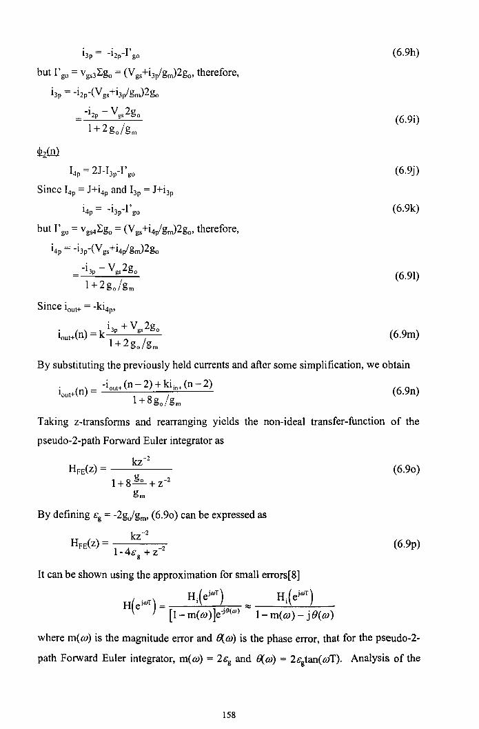
(6.9h)
but I'go = Vgs3~go= (Vgs+i3/gm)2go' therefore,
i3p= -i2p-(Vgs+i3/gm)2go_ -i2p - Vgs2go
l+2go/gm(6.9i)
I4p= 2J-I3p-I' go
Since I4p= J+i4p and 13p= J+i3pi4p= -i3p-I'go
(6.9j)
(6.9k)
but I'go = VgS4~go= (Vgs+i4/g~2go, therefore,
i4p= -i3p-(Vgs+i4p/gm)2go
-i3p - Vgs2gol+2go/gm
(6.91)
Since iout+= -ki4p,
. i3P+ Vgs2golout+(n)= k /
1+ 2go gm
By substituting the previously held currents and after some simplification, we obtain
(6.9m)
. () _ -iout+(n - 2) + kiin+ (n - 2)lout+n - ___.::.:~-_..:....-_:;.:_---l+8go/gm
Taking z-transforms and rearranging yields the non-ideal transfer-function of the
(6.9n)
pseudo-2-path Forward Euler integrator as
kz ?HFE(Z) = -----
1+ 8 go + Z-2
gm
(6.90)
By defining Gg= -2go/gm' (6.90) can be expressed as
kz?H (z)-----FE - 1 4 -2
- Gg + Z(6.9p)
It can be shown using the approximation for small errors[8]
H.(ejIllT) Hi(ejIllT)H(ejIllT) - I ,,___...!...-_- [1-m(m)]e·j6(1lI) ,.., l-m(m)- jB(m)
where m(m) is the magnitude error and ~m) is the phase error, that for the pseudc-Z-
path Forward Euler integrator, m(m) = 2Gg and ~m) = 2Ggtan(mT). Analysis of the
158

z-e-z Forward Euler integrator of Fig. 6.3 will yield mew) = &gand ~w) = >an(wT).
The result is expected, as the delay line in the pseudo-2-path integrator has twice the
number of transistors. This underscores the susceptibility of circulating-delay type
pseudo-N-path structures to finite-conductance ratio errors. Use of gain enhancement
techniques such as cascoding and error correction memory cells[8] will be required to
minimise the errors.
The system poles and magnitude at the resonant frequency are given by
. 1~= ±J /---1+8 go
gm
(6.9q)
Clearly, the poles remain located along the imaginary axis while the gain is inversely
proportional to go/gm. Fortunately, the circuit remains stable as both gm and go are
positive quantities, confining both poles within the unit circle of the z-plane.
Following a similar analysis, the non-ideal transfer-functions of the pseudo-2-path
Backward Euler and bilinear integrators can be derived as:
Backward Euler integrator:
H (z) _ -k(1-3&g)BE - 1 4 -2- &g+ Z
(6.10a)
with corresponding system poles and magnitude at the resonant frequency given by
1+6~
andIHBE(zp)l=k gm8 gogm
(6.lOb)
and
Bilinear integrator:
11 .2k 1--& -z
HB1{Z) = 1- ~E, 1 5 [2 : ] -2
- &g 3 +z1--&2 g
with corresponding system poles and magnitude at the resonant frequency given by
(6.11a)
159
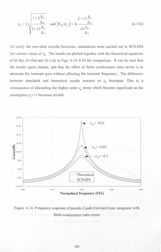
1+ 3 go 2 + 11 go
Zp = ±j gmand !HB1 (zp)! = k
gm (6.11b)1+ 13 go 10 go
gm gm
To verify the non-ideal transfer-functions, simulations were carried out in SCNAP4
for various values of cg. The results are plotted together with the theoretical equations
of (6.9p), (6.l0a) and (6.11a) in Figs. 6.14~6.16 for comparison. It can be seen that
the results agree closely, and that the effect of finite conductance ratio errors is to
attenuate the resonant gain without affecting the resonant frequency. The difference
between simulated and theoretical results worsens as cg increases. This is a
consequence of discarding the higher order cg terms which become significant as the
assumption Cc«1 becomes invalid.
30.00··r-----------------------------,
-~"t:l:510.00c<:c
25.00.
20.00
15.00.
5.00
0.00
·5.00
-Cg= -0.05
- Theoretical······SCNAP4
-10.00+---------+--------t--------t-------~0.00 0.13 0.25
Normalised frequency (fIFs)0.500.38
Figure 6.14 Frequency response ofpseudo-2-path Forward Euler integrator with
finite conductance ratio errors
160

30,00
25,00
20,00
15,00,-~'0'-' 10,00=.;c
5,00
0,00
·5,00
·10.00
0,00
- Theoretical..... , SCNAP4
0,13 0,25 0,38
Normalised frequency (f/Fs)
Figure 6.15 Frequency response of pseudo-2-path Backward Euler integrator with
finite conductance ratio errors
40,00,--------------------------------,
30,00
20,00
10,00.,-~'0'-'.S 0,00c:c
·10,00
·20,00- Theoretical...... SCNAP4
·40,00+--------+-------+--------+---------40,00 0,13 0.25 0,38
Normalised frequency (f/Fs)
Figure 6.16 Frequency response of pseudo- 2-path bilinear Euler integrator with
finite conductance ratio errors
161
0,50
0.50

6.3.2 Clock-feedthrough and Charge-injection Errors
From the circuit of the second-generation SI memory cell of Fig. 6.12, the channel
charge injected by the switch M, into the gate-source memory capacitor Cgs is given
by[8]
(6.12)
where VHis the high voltage level of the clock, Vgs is the gate-source voltage of the
memory transistor, VTS is the threshold voltage, and Ws- Ls the width and length of
the switch. WsLsCox is the switch channel capacitance. The factor a determines the
fraction of charge injected, and depends on the capacitance ratios on both sides of the
switch.
Charge is also injected by the gate-source overlap capacitance, COY'and is given by
(6.13)
where VL is the low voltage level of the clock and Lays is the length of the overlap at
the source side of switch Ms. The total charge injected into the memory capacitor is
thus given by
q = qch + qOY (6.14)
The resulting error voltage across the memory capacitor with an area of WMLMis thus
a(VH - Vgs- VTs)WsLsCox + (VH - VL)WsLovsCox6V= (6.15)WMLMCox
The corresponding error current is
(6.16)
A third source of charge injection occurs when switch M, is in the OFF state. A
voltage transient of 11V at the drain of the memory transistor is capacitively coupled
via the drain-gate Miller capacitor, Cdg' into the gate-source capacitor. This induces an
error voltage of 11Vgs= l1VCdg/(Cdg+Cgs). This problem can usually be minimised by
enhancing the gain using cascode or regulated-cascode[8] topologies. Besides
minimising the drain voltage variation of the main memory transistor, input/output
conductance ratio is significantly improved while the Miller capacitance is
reduced[ 11].
162

By accounting for this charge-injection error with Cc= bIll, and neglecting all other
non-idealities, its effect on the small-signal transfer-function of the pseudo-2-path
Forward Euler integrator( Fig. 6.7 ), can be analysed as follows; Beginning in phase t1
of period (n-2), the current in the memory cells at the end of each respective clock
phase is given by
tlCn-2)
i1p(n-2)= [iin+(n-2)-i4n(n-2)](1-cc)
t2(n-l)
i2p(n-2) = -i1p(n-2)(1-cc)
tI(n-I)
i3p(n-l) = -i2p(n-2)(1-cc)
(6.17a)
(6.17b)
(6.17c)
i4p(n)= -i3p(n-l)(1-cc)
= -[iin+(n-2)+i4P(n-2)](1-cc)4
Substituting for i4 = -io and rearranging gives
iop(n)+iop(n-2)(I-cc)4 = (l-cc)\n+(n-2)
(6.17d)
(6.17e)
Assuming cc«l and taking z-transforms yields the simplified non-ideal transfer-
function for the pseudo-2-path Forward Euler integrator as
H (1-4ce +6ce2)z-2
FE(Z)= 1+ (1- 4ce+ 6c
e2)z-2 (6.17f)
Similarly, it can be shown that the simplified non-ideal transfer-functions of the
pseudo-2-path Backward Euler and bilinear integrator are given as:
Backward Euler integrator:
(6.18a)
Bilinear integrator:
H ()= I-cc -(1-6ce +15ce
2)z-2BI z 2 -2
1+ (1- 4c c +See )z
To simulate the effect of charge injection in SCNAP4, a simplified macro model for a
single memory cell has to be developed. Neglecting channel-length modulation, the
(6.19a)
drain current that is held after sampling can be expressed as
163

Id = j3 (VgS- VT + bY)22
=~ (VgS- VT)2 + ~[2bY(Vgs - VT) + bY2]
The output current is given by
i,= J-Id
In terms of difference equations, this is equivalent to
i,(n) = -iill (n-ll 2) - ~[2bY(Vgs - VT) + bY2]
=-i. (n-1/2)-bYJ2j3J 1+ iin(n-1/2) _fJ bY2
III J 2
(6.20)
(6.21)
(6.22)
To obtain more insight from the unwieldy form of (6.22), a Taylor series expansion of
iinyields
(6.23)
From (6.23), it can be seen that charge injection results in offset, gain and non-
linearity or distortion errors as indicated by the first, second and higher order terms
respectively. Ideally, bY = 0, and (6.23) reduces to the familiar io(n) = -iin(n-1I2) of
an ideal memory cell.
Offset and signal dependentcharge injection circuit
D Sample phase: ¢lHold phase: ¢2
+s Bias current
source
Figure 6.17 Charge injection macromodel ofmernory cell
164

It was decided to incorporate only the offset and gain errors into the memory cell
macromodel given that SCNAP4 is capable of simulating only linear systems. This is
a reasonable assumption, as for small signals the error function is linear to a first order
approximation. With large signals, gm and the charge injected, q, will vary non-
linearly to produce harmonic distortion(see Fig. 6.40).
The operation of the charge inj ection model of Fig. 6.17, neglecting the effect of go is
described as follows: During the sampling phase( ¢I), the circuit is diode-connected
with the drain/D) and gate(G) shorted. Capacitor Cj is charged up by the bias current J
and i., to the ideal voltage of VgSi.Throughout this time, the offset, Vos = -vojeoj, is
shorted to ground. During the hold phase(¢2), Cgs charges up to Vgs= ejVgSi+Vos,
and the drain current becomes Id = gmVgs- Because the bias current J is always
connected to the drain, the output current is therefore given by
i,= J-Id
= J-gmVgs
= J-gm(ejVgSi+Vos)
= J-ej(iin+Jj-g.,Vos
= Jt l-ejj-g., Vos- iinej (6.24)
By defining ej = I-Be' (6.24) becomes
(6.25)
Clearly, (6.25) is a linear approximation of (6.23), where the offset and gain errors are
governed by eoj and ej = I-Berespectively. Equating (6.25) to (6.23) yields
B = -bY f7fc Vu
eoj = _1 [bY (7jJ+ f3 bY2]
gm VT 2
(6.26)
The simulated output of a second generation memory cell using the charge injection
model is shown in Fig. 6.18. The signal dependencers, = 0.05) of the charge injection
error is evident and the effect of an injected offset(Vos = 0.05V) error is also shown.
The model used for mirror-connected outputs to realise filter coefficients is shown in
Fig. 6.19. Both the bias current source and gmare scaled by k.
165

1.00 ~
1.20 -,-------------------------------,
0.80 ~
Q;j 0.60 ~..QJ- 0.40-co:~ 0.20·iii't:l 0.00QJ
'".- -0 20 ~-;.E -DAD
eZ -0.60 ~
-0.80
-1.00
-_ Input signal
Output signal(inverted)Cc = 0.05, Vos = OV
Output signal(inverted)Cc = 0.05, Vos = O.05V
0.10 0.20
-1.20 -f----t-----t---+---t----I---+---t-----!----+------10.00 0.70 0.80 1.000.30 0.50 0.60 0.90
Figure 6.18 Simulated output current of a memory cell based on the charge-injection
model
0.40
Time(uSecs)
D
kgm
+s Bias current
source
Figure 6.19 Macromodel for mirror-connected output transistors
The three pseudo-2-path integrators were simulated with SCNAP4 using the models
just described for different values of cc. In a small-signal AC simulation, the DC
voltage sources will be shorted to ground, nullifying the effects of the offset. To
account for the effects of the offset voltage, an impulse response of the network has to
166

be obtained in a transient simulation and processed by FFT. However, both
approaches will yield almost identical results in the frequency domain as the offset
component will appear as just a peak at DC.
The results of the simulations are plotted together with the respective theoretical
transfer functions of(6.l7~6.l9) in Figs. 6.20~6.22. It can be seen that the results are
in close agreement. The effect of charge injection errors on the frequency response of
the pseudo-2-path integrators is to attenuate the resonant gain without affecting the
resonant frequency. This is similar to the effect of finite conductance ratio errors of
the previous analysis. The difference observed between the simulated and theoretical
results worsens as Cc increases. This is a consequence of discarding the higher order Cc
terms which become significant as the assumption cc«l becomes invalid.
30.00
25.00 -
20.00
15.00--~"'0'-' 10.00 --=.;c
5.00 -
0.00
·5.00
-10.00
0
-Ec=0.05
- TheoreticalSCNAP4
0.125 0.25 0.375 0.5
Normalised frequency (f/Fs)
Figure 6.20 Frequency response of the pseudo-2-path Forward Euler integrator with
charge injection errors
167

30.00,-------------------------------
25.00 -
5.00
20.00
15.00-~~.S 10.00
~c
0.00
- TheoreticalSCNAP4
-10.00+---------+--------;---------+--------1o 0.125 0.25
Normalised frequency (fIFs)0.375 0.5
Figure 6.21 Frequency response of the pseudo-2-path Backward Euler integrator
with charge injection errors
40.00
30.00
20.00-
10.00-~"0-- 0.00=.;e
-10.00
-20.00
-30.00-
-40.00
0
-Ec=O.05
- Theoretical······SCNAP4
0.125 0.25 0.375 0.5
Normalised frequency (f/Fs)
Figure 6.22 Frequency response of the pseudo-2-path bilinear integrator with charge
injection errors
168

6.3.3 Settling Errors
Settling errors originate from incomplete charging of the memory capacitor Cgs within
the duration of the sampling phase. This results in an error in the output current,
which is sampled by subsequent stages. It has been shown[8] that the dynamics of a
second-generation SI memory cell can be described by a second order lowpass
transfer function with the pole frequency and Q-factor given by
ill =o and (6.27)
where r, is the switch-ON resistance of transistor M, in Fig. 6.12. For stability
reasons, an overdamped(Q<O.5) response is desired, in which case, the settling error Gs
is given[8] by
Gs= J 1 [(1+Jl-4Q2)exp(2 1- 4Q2
-(1-~1-4Q' )exp( (6.28)
where ts is the settling time.
In the following small-signal analysis, we will consider the effect of settling error on
the frequency response of the pseudo-2-path Forward Euler integrator(Fig. 6.7). We
begin the analysis starting in phase t1 of period (n-2), where the duration of each
phase defines the settling time ts'
tHn-2)
The incremental current in transistor M1P is
iin+(n-2)-i4n(n-2)-i1p(n-2) (6.29a)
At the end of this phase, incomplete charging by the incremental current results in the
current stored in M1pof
i1p(n-l) = ilp(n-2)+[iin+(n-2)-i4n(n-2)-ilp(n-2)](I-Gs)
(6.29b)
t2(n-l)
The incremental current in transistor M2pis
169

(6.29c)
At the end of this phase, incomplete charging by the incremental current results in the
current stored in M2pof
i2p(n-l) = i2p(n-2)+[-ilp(n-l)-i2P(n-2)](1-ss)
= ssi2p(n-2)-(1-ss)i1p(n-l)
Rearranging,
(6.29d)
tICn-I)
The incremental current in transistor M3pis
-i2p(n-l )-i3p(n-l) (6.2ge)
At the end of this phase, incomplete charging by the incremental current results in the
current stored in M3pof
i3p(n)= i3p(n-l )+[ -i2p(n-l )-i3p(n-l )](l-ss)
(6.29f)
Rearranging,
i2p(n-l) = ~i3P(n-l) __ 1-i3P(n)l-c l-cs s
(6.29g)
t2(n)
The incremental current in transistor M4pis
-i3P(n)-i4p(n-l) (6.29h)
At the end of this phase, incomplete charging by the incremental current results in the
current stored in M4pof
i4p(n)= i4p(n-l )+[ -i3p(n)-i4p(n-l)](l-ss)
(6.29i)
Rearranging,
. ( ) cs. ( 1.13 n = --1 n-1)---1 (n)p l-c 4p l-c 4ps s
(6.29j)
By back substitution and some rearranging, we obtain
iout+(n)= (1-cs)\n+(n-2)+4csiout+(n-l )-[6cs 2+(1-cs)4]iout+(n-2)+4c/iout+(n-3)-cs4iout+(n-4)
(6.29k)
From (6.29k), it can be seen that the settling error produces residual, or memorised
errors related to signals from earlier clock cycles in addition to attenuating the input
170

signal. Taking z-transforms and after some simplification yields the transfer-function
of the pseudo-2-path Forward Euler integrator as
H()- (1-48s+68s2)z-2
FE z - ----'--___.::_----"-'----,--1- 48 Z-1+ (1- 48 + 128 2)Z-2s s s
(6.291)
The system poles are given by
Zp= 28s±j~1-48s+88s2 (6.29m)
Clearly, settling error displaces the poles from the imaginary axis by 285 apart from
attenuating the gain at resonance. The non-ideal transfer-function of the pseudo-2-
path Backward Euler and bilinear integrators can similarly be derived as:
-1+8 +38 (1-8 )z-I-3& 2Z-2H (z) = s s s s
BE 1-48 Z-1+(1-4& +128 2)Z-2s s s
(6.30a)
(6.31a)
To verify the analyses, simulation was performed for different values of &sobtained
using (6.27) and (6.28) for the overdamped condition. The results are shown in Figs.
6.23-6.25 for both the theoretical and simulated responses. Settling error thus
attenuates the gain and lowers the resonant frequency. This is detrimental to
narrowband bandpass systems where stability of the passband centre frequency is
crucial. Therefore, adequate time must be provided for settlingf--Zr where 't=lIcoo)[8]
in order to minimise these errors. This imposes an upper limit on the highest
achievable clock frequency. The error between theoretical and simulated responses at
larger values of &5for the bilinear integrator is mainly due to the simplification of an
otherwise large and unwieldy non-ideal theoretical transfer-function. It should be
noted that 85 = 0.01 represents an error of 1% while most practical circuits are
designed to settle to within 0.1%.
171

30.00
25.00 ..
20.00
15.00.-="0-- 10.00 .Cl....(IS
I-'5.00 .
0.00 .
-5.00 --
·10.00 .
0.00
.. .... SCNAP4
- Theoretical
0.13 0.25 0.38
Normalised frequency (f/Fs)0.50
Figure 6.23 Frequency response of the pseudo-2-path Forward Euler integrator with
settling errors
30.00
25.00
20.00 --
15.00.-="0-- 10.00Cl.;I-'
5.00
0.00
-5.00 .
-10.00
0.00
...... SCNAP4
- Theoretical
0.38 0.500.13 0.25
Normalised frequency (f/Fs)
Figure 6.24 Frequency response ofthe pseudo-2-path Backward Euler integrator
with settling errors
172

40.00,..-----------·-------------------,
10.00
85=0.1
20.00
30.00
$'"Q'et 0.00'.;I-'
·10.00
·20.00······SCNAP4- Theoretical
·30.00 f
.40.00+- ---1 -+- -+- --11-1
0.00 0.13 0.25 0.38 0.50
Normalised frequency (f/Fs)
Figure 6.25 Frequency response of the pseudo-2-path bilinear integrator with settling
errors
6.4 SWITCHED-CURRENT N-PATH AND PSEUDO-N-PATH LADDER
FILTER DESIGN
An N=2 path and a pseudo-2-path 6th order narrowband bandpass filter serve as
examples to illustrate the usefulness of the proposed cells. The z-domain SFG of a
bilinear-transformed, 3rd order elliptic lowpass reference filter is shown in Fig. 6.26.
The design specifications and transistor ratio coefficients are listed in Table 6.2.
Examination of the reference SFG shows that it consists of Backward Euler
integrators ~, a Forward Euler integrator \jf, and a bilinear integrator at the input
formed by the input branch X12A. and the first ~ branch.
6.4.1 Switched-Current N-Path Ladder Design
The transformation process is achieved by simply replacing the integrators within the
SFG by their corresponding transformed versions(Figs. 6.3-6.5). The feed-through
signals represented by branches with the factor Il=(l-Z-l) are connected to the
respective summing nodes immediately following the input sampling switches. To
173

replace the A input branch by the transformed bilinear integrator, the output of the
bilinear integrator has to be connected to the summing node of the first Backward
Euler integrator instead of the integrating input. The resulting z~ -z transformed path
filter is shown in Fig. 6.27 without the bias circuits to highlight the connectivity. To
achieve the z~ _Z2 transformation for a bandpass response, two path filters in parallel
are sampled in a time interleaved manner as shown in Fig. 6.28. For a two phase
clock, this simply involves opposite phase sequences for both paths. A sample-and-
hold is required for each path as the bilinear input stage samples on both phase t1 and
t2. Each path is sampled at 10MHz for an overall rate of 20MHz.
Xs_~----I~-,---+---~~-+--o Vout
Figure 6.26 SFG of bilinear-transformed, 3rd order elliptic lowpass reference filter
Table 6.2 Design specifications and transistor ratio coefficients of the prototype
lowpass filter
Design specifications of 3rd order lowpass prototype filter
Passband Edge 1kHz Passband Ripple 0.5dB
Stopband Edge 2kHz Stopband Attenuation 30dB
Transistor ratios
X4 0.092297 X7 0.079797 XIO 0.038763
Xs 0.177828 Xs 0.045229 Xli 0.038763
X6 0.057488 X9 0.032585 XJ2 0.027926
Transistor Spread: 35.8 Clock Frequency: 10MHz
174

Bilinearinput stage
BackwardEulerintegrator
integrator
)
, lout+
lout-
Figure 6.27 Switched-current highpass path filter by z~ -z transformation
175

~~~~~~~~~ ~~~~~LYFILTER 1 : u,
. lin- (tl t2) Iout- ;_-7"
Rp
:~~~~ ~~~~ ~~~~~l_3,FILTER 2 : tL
. lin- (t2 tl ) Iout- ;.._...7"
Figure 6.28 Structure of the N=2 path switched-current filter
6.4.2 Switched-Current Pseudo-N-Path Ladder Design
The pseudo-N-path design is more straight-forward as each cell in Figs. 6.7-6.9 performs
the z~ _Z2transformation. The integrators within the SFG are simply replaced by their
corresponding transformed versions following the rules previously described. The only
exception is that the output polarity of the Forward Euler integrator has to be reversed,
which can be achieved by simply crossing the output signal pairs(shown shaded in Figs.
6.29a and 6.29b). This is required as the integrator circuit is non-inverting(Fig. 6.7), while
a proper z~ _Z2transformed Forward Euler integrator transfer-function is inverting(Table
6.1). A full period sample-and-hold circuit is required at the input if the filter is preceded
by a bilinear integrator. The simplified schematic less the bias current sources is shown in
Fig. 6.29a. Alternatively, the (1-z-2) circuit of Fig. 6.10 can be cascaded at the output of the
pseudo-2-path filter as shown in Fig. 6.29b. Both filters have to be clocked at 20MHz to
fulfill the equivalent of two time-interleaved, 10MHz sampled circuits. The simulated
amplitude responses of both the N-path and pseudo-N-path filters are shown in Fig. 6.30.
Clock-feedthrough noise is far removed from the passbands, as the harmonics occur at
multiples of 10MHz and 20MHz for the N-path and pseudo-N-path filters respectively.
The slight loss observed in the passband is due to the sin(x)/x hold-function with a first zero
at 20MHz. Although the filters can have either a bilinear input stage or an FIR output stage
of (1_£1) or (1-z-2) for the N-path and pseudo-N-path types respectively, the latter is
preferred in view of dynamic-range scaling requirements. This is illustrated by Fig. 6.31,
which shows the output level of the integrators within the filter after dynamic-range scaling
176

for the bilinear input stage case. It is obvious that the bilinear integrator output will
saturate well in advance of the other integrators due to the huge gain peak in the centre of
the passband. This problem can be circumvented by replacing the bilinear integrator at the
input by FIR stage at the output, as illustrated for the pseudo-2-path case in Fig. 6.29b.
6.4.3 Sensitivity and Non-Ideal Factors
Several non-ideal factors affecting the N-path and pseudo-N-path filters are considered
next. It is well known that the sensitivity of bandpass filters increases with the Q-
factor[ 10]. For a directly realised narrowband bandpass filter, the Q-factor is
approximately QBP~(2wo/B)QLP'where Wo is the centre frequency of the bandpass response
and B is the bandwidth[lO]. With wo»B/2 for narrowband bandpass filters, QBP»QLP.
Thus, as the N-path and pseudo-N-path filters use a lowpass reference, they do not suffer
from the problems associated with high Q's as in a directly realised bandpass filter. For
instance, transistor spread in the first two designs is 35.8 and in the latter, 68.24.
The overall passband sensitivity of the N-path and pseudo-N-path filters to deviations in the
transistor ratios are compared to a conventional, directly realised bandpass filter of
equivalent specifications in Fig. 6.32. Superiority is clearly exhibited over the conventional
bandpass filter, which apart from having a high overall sensitivity, is extremely sensitive at
the passband edges. This is illustrated in Fig. 6.33, which shows the effect on the
amplitude responses for a + 1% deviation in all the transistor ratios. The amplitude
response of the N-path and pseudo-N-path filters are virtually unaffected while distortion of
the passband shape, and more seriously, a frequency shift is observed for the conventional
bandpass filter.
177

lin+lin-
Bilinearintegrator
BackwardEulerintegrator
integrator
lout+
lout-
Backward Euler integrator
Figure 6.29a Switched-current 6th order pseudo-2-path bandpass filter with bilinear
integrator input stage (Version 1)
178

BackwardEulerintegrator
ForwardEulerintegrator
BackwardEulerintegrator
(1_z-2) FIR output stage
Figure 6.29b Switched-current 6th order pseudo-2-path bandpass filter with (1_z-2) FIR
output stage (Version 2)
179

-10.00
-20.00
-.~ -30.00
'-'Q)'Q.E -40.00._Q..~ -50.00
-60.00
-70.00
-80.00 -II-------t------+-------+------t------+lO.OOE+OO 2.00E+06 4.00E+06 6.00E+06 8.00E+06 1.00E+07
Frequency(Hz)
Figure 6.30 Ideal amplitude response of the narrowbandbandpass filters
40.00.,...-------------------------------,
Output of bilinear integrator
/
Output of first BackwardEuler integrator
L"./ / '",~~:.:..:. -- - .
"./~
/1 Output of first Forward Euler integrator1//'/ Output of last Backward Euler integrator
1
30.00 .
20.00-~"Cl'-' 10.00Q)
"Cl
=........Q.. 0.00e-<
-10.00
-20.00
",,,"",,
"""""""""\ "-30.00 1+----+----\----+-------;----+-----+----,.----.....,.,4.80E+06 4.85E+06 4.90E+06 4.95E+06 5.00E+06 5.05E+06 5.IOE+06 5.15E+06 5.20E+06
Frequency(Hz)
Figure 6.31 Dynamic-range scaled output level of integratorswithin the pseudo-N-path
filter realisation(Version 1) with a bilinear integrator input stage
180

350.00
: --.300.00
"
250.00-.~0-...==';I 200.00 -'--'~ -DIRECT........> -o--N-PATH.... 150.00........~= -x- PSEUDO-N PATHQ.lrJ'1
100.00
50.00
0.00
4.80E+06 4.8SE+06 4.90E+06 4.9SE+06 S.00E+06 S.OSE+06 S.JOE+06 S.15E+06 5.20E+06
Frequency(Hz)
Figure 6.32 Comparison of overall passband sensitivity for the pseudo-N-path, N-path
and a direct bandpass realisation
-10.00
.:
-20.00--==';I~ -30.00';I
!4000~'\'j-50.00 \~ ". !
\ .. .-60.00 , :
...... DIRECT-o--N-PATH-x- PSEUDO-N PATH
-70.00 +-----~------t----__+----_+----_+_---__14.70E+06 4.80E+06 4.90E+06 5.00E+06 5. JOE+06 S.20E+06 S.30E+06
Frequency(Hz)
Figure 6.33 Effect of +1% deviation in transistor coefficients on amplitude responses
181

Pseudo-N-path se filters are known to be particularly affected by the finite gain of the
amplifiers[3,5]. In SI, this is equivalent to the effect of finite output/input conductance
ratio (gO/gm)of the transistors, which should ideally be zero. The different filter versions
were simulated with Sg = -2go/gm set at 0.1%. The simulated amplitude responses shown in
Fig. 6.34. Version-2 of the pseudo-N-path filter suffers the most attenuation in the
passband while the N-path filter is the least affected. It is also interesting to note that
version-l of the pseudo-N-path filter is more robust that the direct realisation and differs by
only less than -0.5dB compared to the N-path filter. The passband of the direct bandpass
filter is shifted slightly off the centre frequency. In all, this highlights the need to realise
the actual circuits using gain enhancement techniques and memory cells[8] to minimise the
transmission errors.
O.OO,_-------------------------,
-1.00
$' -2.00't:l'-'~'t:lE -3.00
0..
~ -4.00
-S.OO --
-6.00+----+---iQ-I--+----+----+----+---~_\_QI_-_+_---4.80E+06 4.85E+06 4.90E+06 4.9SE+06 S.00E+06 S.OSE+065.IOE+06 S.15E+06 S.20E+06
Frequency(Hz)
Figure 6.34 Effect of finite conductance ratio errors on the frequency response of the
different bandpass filters
Next, the effect of charge injection errors on the different realisations were simulated with
Se = 0.1%. The results in Fig. 6.35 indicate a superior N-path filter while the other
realisations are -0.5dB lower in comparison. This again illustrates the weakness of
circulating-delay type pseudo-N-path structures to cumulative errors against the N-path
design. Error correction memory cells[8] used in conjunction with dummy transistors
182

should sufficiently reduce the injected charge, as will be demonstrated in the following
section for a cascoded S21 memory cell with Be < 0.05%.
0.00-
-5.00-l----+--J+-.._+__----+----+----I-----+--I-I---+----12.40E+06 2.43E+06 2.45E+06 2.48E+06 2.50E+06 2.53E+06 2.55E+06 2.58E+06 2.60E+06
-3.50 ······DIRECT I Gc=O.l%-o-N-PATH L. .....J
-x- PSEUDO-N-PATH(Ver.l)-0- PSEUDO-N-PATH(Ver.2)
·0.50
·1.00..
-1.50,-..~~ -2.00~'0E -2.50
0.8 -3.00
<
-4.00
-4.50
Frequency(Hz)
Figure 6.35 Effect of signal dependent charge-injection errors on the frequency response
of the different bandpass filters
10.00.---------------------------------,
0.00 .
..· .. ·DIRECT 1
l6's=O.l %-o-N-PATH .-x- PSEUDO-N-PATH(Ver.l~ PSEUDO-N-PATH(Ver.2
-50.001----I-----+---l<r----r---+---+---+-__:--+-4I----+----+---~
-40.00
4.50E+06 4.60E+06 4.70E+06 4.80E+06 4.90E+06 5.00E+06 5.108+06 5.208+06 5.30E+06 5.40E+06 5.508+06
Frequency(Hz)
Figure 6.36 Effect of settling errors on the frequency response of the different bandpass
filters
183

Effect of settling errors with Ss = 0.1% can be seen in Fig. 6.36. The frequency response of
the direct realisation is severely distorted, affecting both the passband and stopband,
rendering the design virtually useless. The distortion in the passband of the version-l
pseudo-N-path filter is caused by a shift in the resonant peak of the bilinear input stage,
resulting in mismatched cancellation. This is another negative aspect of having a bilinear
integrator at the input. The difference in having a (l-Z·2) FIR stage at the output instead of
the input bilinear integrator can be seen in the response of the version-2 pseudo-N-path
filter, where no such distortion exist in the passband. The best response is due to that of the
N-path filter, where both distortion and attenuation are minimum.
Thus far, the N-path realisation seems to deliver the best overall performance. This is
expected as the overall transfer function is the same as that of each individual path, which
does not suffer from the cumulative errors as much as a single path, circulating delay
pseudo-N-path filter. However, one important advantage of the pseudo-N-path method
over the N-path method is the absence of mirror-frequency noise that results from mismatch
between path filters. The generation of mirror-frequency noise imposes a major limitation
on the viability of N-path realisations, and will thus be examined next. From Fig. 6.28, it
can be seen that for a 2 path structure, the overall sampling frequency, Fs, is twice that of
the path clock frequency, Fsp. The input sequence Yin is a time-interleaved, vector sum
described by
Vin(z) =VinJ(z)+Vin2(z)
where the subscripts 1 and 2 denote path 1 and path 2 respectively. At the output, the
signals from both paths sum to give
Vout(z) =VoutJ(z)+Voutz(z)
Since the transfer functions of both the paths are nominally equal, we can write
Vout.tz) = H(z)VinJ(z)
Vout2(z) = H(z)Vin2(Z)
and the overall transfer function works out to
H(z) = Vout(z) = Voutl(z) + Vout2(z)Vin(z) Vin, (z) + Vin, (z)
Consider the case when there is asymmetry between the path filters. A mismatch error in
path 2 will alter its transfer function to become H2(z) = (1+s)H(z), which gives
184

Vout(z) _ H(z)Vinl (z) + (1+ 8)H(z)Vin2 (z)Vin(z) Vin, (z) + Vin, (z)
This can be expressed as
Vout(z) = H(z)[Vin(z)+8Vin2(z)]
When both paths are matched, &=0,and Vout(z) = H(z)Vin(z). Since each individual path
is clocked at the lower sampling frequency of Fsp, a mismatch in the gain of path 2 thus
generates attenuated spectral content at nFsp ± ~n' where (n=l, 2, ....JN12l), IN/2l denotes
the integer part of NI2 and ~n is the input signal frequency[10]. Ideally, these signals are
equal in magnitude and cancel out due to a phase shift of 7t for a 2-path structure. Fig. 6.37
shows the characteristics of mirror-frequency rejection for the N-path and pseudo-N path
filters.
0,00,--------------------------,
~~'u -100,00
=~6- ·120,00~:..~:..e:..:..~
IDEAL N-PATH
+1% PATH MISMATCHN-PATH-20,00.-
~~ -40,00=o;::u~.....,~
-60,00
-80,00
·180,00
·200,00+-----+-----+-----+-----+-----1------14.70E+06 4,80E+06 4,90E+06 5,00E+06 5,IOE+06 5,20E+06 5,30E+06
Frequency(Hz)
Figure 6.37 Mirror frequencies rejection in the vicinity of the passband region
Input signal frequency was swept from 4.7MHz-5MHz and 5MHz-5.3MHz while plotting
the output from 5MHz-5.3MHz and 4.7MHz-5MHz respectively. Under perfect matching
conditions for the N-path filter, the rejection in the passband is -120dB. This level of
rejection deteriorates drastically to about -40dB when a mismatch of +1% is introduced in
one of the path filters. When the structure of the path filter is complex, as in this case of a
185

third order z~-z transformed filter, the relationship between mismatch and the level of
rejection is difficult to quantify. This is because the magnitude response sensitivity of the
different components is topology dependent. However, for the simple case when mismatch
is directly related to gain, such as for scaled output mirror transistors, the level of rejection
is determined by 2010glO(&/N). Thus, if the passband sensitivity is low, as in this case, the
level of mirror frequencies rejection can be approximated by 20l0glO(O.OI/2) = -46.02dB
for a OdB reference level(Fig. 6.37). Although no path mismatches are possible in the
pseudo-N-path filter since there is only one physical path, its rejection characteristic is
plotted for comparison, this shows a level of -I40dB.
Finally, noise simulations were performed to compare the different filters. A InA! JHz.drain-referred noise current was used as a unit reference. The noise generators associated
with the filter coefficients were scaled in proportion to the root of the respective
transconductances. Effects of noise foldback within the arbitrarily defined noise-bandwidth
were considered.
-120.00' --'---,--
---g -125.00....I.0"~=- -130.00't:I-- ";, ,..-C -135.00 . ..... ··..--1.~ .'t:I -140.00
';I.....~ -145.00Q.,
'"Cl).~ -150.00Q
Z
........... DIRECT ..--/ "."" _ .
PSEUDO-N-PATH
N-PATH
-155.00 I------+-----t----_I-- -+- -t- -----j
4.70E+06 4.806+06 4.90E+06 5.00E+06 5.IOE+06 5.20E+06 5.30E+06
Frequency(Hz)
Figure 6.38 Simulated noise spectral densities with an arbitrary, fixed noise-bandwidth
for the pseudo-N-path, N-path and a direct bandpass realisation
186

Fig. 6.38 shows the typical simulated norse spectral densities companng the N-path,
pseudo-N-path and a conventional bandpass filter. The direct realisation has the highest
noise level within the passband while the N-path filter has a noise level that is about lldB
lower compared to the pseudo-N-path filter.
6.5 CIRCUIT IMPLEMENTATION ISSUES
6.5.1 Memory Cell
The first step towards a circuit level implementation is to design an optimised memory cell.
As seen from the simulations in the previous section, the non-ideal errors will have to be
kept well below 0.1% to achieve a reasonably accurate response. An 821[12] type memory
cell was chosen to minimise both clock-feedthroughlcharge-injection errors. Dummy
transistors were attached to both the coarse and fine sampling switches to further reduce
the injected charge. To minimise finite conductance ratio errors, the output resistance of
the memory cell was increased using fixed bias cascode transistors. The memory cell is
shown in Fig. 6.39.
YDD
YBiasl
YBias2 D---+----l
yeas D---+----l
YSS
¢1 I¢lax r--L_l__j¢la rL_l_j¢lb~ . . .. . .~ \ I \¢2ax r--1~:--~¢2a n\.;.: ~_ __.;.,¢2b~
Figure 6.39 Cascoded 821 memory cell and clock waveforms
187

The current transfer clock phases are overlapping to minimise transient glitches while the
voltage sampling clock wave forms have to be non-overlapping. Designing an optimised
cell is a complicated procedure involving many trade-offs[S] and careful considerations
have to be given to ensure that the transistors stay saturated at all times. For the transistors
in the bias chain MJ and MJC' the critical condition arises during the 'coarse' sampling
phase (¢1 a) when the input signal is at a maximum:
VDD-VgsI >VdsatJ+VdsatJC
VDD-[Vr+(Vgs-Vr)l.Jl + m] > (Vgs-Vr)J+(Vgs-Vr)Jc
where the modulation index is defined as the ratio of the input current to bias current, m =
iin/J. Therefore, the transistors in the bias chain stay saturated provided
(Vgs-Vr)J < VDD-Vr(VgS-Vr)l.Jl + m -(Vgs-Vr)JC
A second critical condition occurs during the hold phase( ¢2) when the first memory cell is
sinking the maximum current from a second memory cell connected in cascade[S]. Thus in
phase ¢2, the second memory cell will be diode connected and have a minimum drain
current. This minimum gate voltage of the second cell, Vgs2'will have to be high enough to
ensure transistors M I and Mc of the first cell, which are sinking maximum current, stays
saturated:
Vgs2> VdsatC+Vdsatl
Vr+(V gs"Vr)2 .Jl- m > .Jl + m [(Vgs-Vr)j+(V gs-Vrk]
Therefore, in this situation, transistors M, and Mc of the first cell stay saturated provided
VT -(VgS - VT)C~(Vgs-Vr)l = (Vgs-Vr)2 = (Vgs-Vr)::;; rr+; tr=:
-vl+m--vl-m
The supply voltage VDD was set at 3V (VSS=OV). VBiasl was chosen to be mid-rail at
1.5V, which will ensure that the current summing node stays close to 1.5V during the 'fine'
correction phase, ¢l b. Using models from an AMI double metal 1.OJ.lmdigital CMOS
process, the transistor dimensions designed for a bias current of approximately lOOIlA and
a maximum modulation index of m = ±O.S is given in Table 6.3. The memory cell was
simulated in HSPICE and the normalised DC transfer characteristic curves are shown in
Figure 6.40.
188

Table 6.3 Specifications of the SI memory cell
Transistors (WIL) in urnBias current, MJ 42/2Bias cascade, MJC 80/1Memory cascade, Mc 30/1Main memory, M] 50/4Current transfer switches 20/1Sampling switches 311Bias current 100)..tAVDD(VSS=OV) 3VVBiasl 1.5VVBias2 1.2VVCas 1.8V
1.00 -0.033000
0.80 --- lout -tt- lerror- -0.033500.... 0.60 ....c: c:~ <II
loo looloo 0.40 loo= -0.034000 =IJ IJ....
0.20 loo= 0C. loo.... loo= 0.00 -0.034500 ~0 "0"0 ~~ -0.20 .:!l.:!l -;-; -0.035000 ee -0.40 looloo 00 ZZ -0.60
-0.035500
-0.80 -
-1.00 -0.036000
-0.80 -0.60 -0.40 -0.20 0.00 0.20 0.40 0.60 0.80
Modulation index (m)
Figure 6.40 DC transfer characteristics of the cascaded S2Imemory cell
6.5.2 Common-mode Control
The proposed N-path and pseudo-N-path cells are all fully-balanced and therefore require
some form of common-mode control circuitry. One option is a common-mode feed-
forward(CMFF) circuit[15] as shown in Fig. 6.41. The circuit operates by sensing the
differential gate voltage at the output of the integrators using half size transistors Mcp and
189

MeN' The ideal common-mode current drawn will be 2(0.5J) = J when only differential
signals are present. This current is then mirrored by the PMOS transistor MMIRto two
outputs biased by currents of magnitude J. Thus, ideally, both the generated common-
mode currents IeMwill be zero. When undesired common-mode signals are present, they
will be sensed by Mep and MeN and IeMs of the appropriate polarity generated to cancel
them out when both the outputs of the integrator and CMFF circuit are summed.
"Mi'~~~~~d'~~'tp~'t'~f'i~t'~g~~t~~"""'"VDD \. VDD
...........................................
VSS
' (:.«:l.~~.«:l.~:m,~~~.f.~~~~.(~rw.~r".~~r~.~~~ ....
Figure 6.41 Common-mode feedforward correction scheme
There are several disadvantages with this scheme. Firstly, the common-mode signals that
are present in the integrator itself are not eliminated. This might shift the bias point of the
memory cells and cause some transistors to cutoff if the common-mode signals become too
large. Secondly, correction of common-mode levels is afforded only to one output
balanced pair. To correct more than one output, which is usually the case for filters with
190

multiple coefficients, current mirrors will be required for each additional output. Another
option is to use a common-mode feedback circuit as shown in Fig. 6.42 .
..... - ~
Output ofintegrator
VDD
: ¢2: ..!Y __ -+- ......._-:-- __ --,: _/-- -----t---,
¢2
.'.........................................
VSSVDD
VSS
...........~~~~~~.":~.~.~~ .f~~4~.~.<;~.~~r.<;.1:1:~~ ....
Figure 6.42 Common-mode feedback correction scheme
Transistors Mp! to MP4 form two PMOS differential pairs biased by currents J. VCMsets
the desired common-mode voltage level, which is usually the diode-connected memory cell
gate voltage with zero input. With only differential signals present, an increase in current
in Mp! is met by a proportional decrease in MP4. Thus, equal currents flow in Mp! and Mp3
and similarly, in Mp2 and MP4• The current that flows to the load ML and the current mirror
MMIRare thus equal to J. Since the two mirror outputs are biased by currents of magnitude
J, the output currents of the CMFB circuit, ICM'are ideally zero. If the common-mode level
191

is increased during sampling(phase rjJ2), this will be reflected by an increase in the
common-mode gate voltages of G, and GN. This will be sensed by Mpl and Mp4, which
reduces the current to the load ML while increasing the current to MMIR. The increase in
mirrored current will make both IcMs negative, reducing the common-mode currents to
transistors MIP and MIN of the integrator. Therefore, the current that is sampled is free
from unwanted common-mode signals. Any additional mirror transistors that are connected
to gates Gp and GN to realise filter coefficients will also be free from common-mode
signals. Thus, only one CMFB circuit is needed at the output of each integrator to ensure
that no common-mode signals remain in the integrator and get propagated to subsequent
circuits. For the differential pairs, high output impedance cascodes are required for the bias
current sources to maintain a high common-mode rejection ratio(CMRR). A sufficiently
large CM loop gain has to be provided by the transconductance of the differential pairs to
ensure effective feedback correction. To adapt this to S21 cells of Fig. 6.39, a
complementary type CMFB circuit will be required to operate during the 'fine' sampling
phases( rjJlband rjJ2b).
6.5.3 A 6th Order Pseudo-2-Path SI Bandpass Filter
The Version-2 pseudo-2-path filter structure of Fig. 6.29b was designed using cascoded S21
cells of Fig. 6.39 and CMFB circuits of Fig. 6.42 are attached to the outputs of the three
constituent integrators. Before proceeding with simulation, the coefficient transistors at
each integrator output has to be settle-scaled to ensure their combined gate areas are the
same as that of a single optimised cell while realising the required filter coefficient ratios.
For the optimised unit memory cell of Fig. 6.39, WMlopt=50j.lmand LMlopt=4j.lm.This gives
the ratio Ropt= WM1op!LMlopt= 12.5 and area Aopt= WMloptLMlopt= 200j.lm2• To find the
scaled dimensions WM1 and LMI for the transistors connected at the output of the first
Backward Euler integrator, the two inequalities that must be satisfied are Aopt =
WMILMl(1+XS+Xg+Xs) and WMI= RoptLMI. Therefore,
and
and the scaled widths of the coefficient transistors are WM1XS, WM1Xg and WM1XS, with a
common gate length of LM1. This procedure has to be repeated for the bias transistors too,
192

as they sample in the 'fine' memory phases(¢lb and ¢2b). The outputs of the remaining
integrators have to be similarly scaled.
The circuit was simulated in HSPICE by impulse excitation and the output was processed
by FFT in MATLAB. The reason for adopting this approach is that the passband is
centered around a quarter of the sampling frequency. This low signal-to-clock frequency
ratio makes the peak-to-peak output signal levels difficult to determine if the conventional
way of performing transient sweeps at different input signal frequencies were carried out.
The response obtained is plotted together with a SCNAP4 simulation in Fig. 6.43. Charge-
injection models with an error of Be = 0.045%, obtained from the gradient of an
approximated best-fit line to the error characteristics in Fig. 6.40, was used in the SCNAP4
simulation.
10.00 ,-----------------------------, 4.00
0.00
-10.00..-.,~'0'ar -20.00'0::l......_Q. -30.00e<
-40.00
-50.00
~ Left scale
Right scale ~
3.50
$3.00 '0---.;.....
Q,l
250 '0. '0
=~r" ,Q
(I.l
2.00 ~
~
1.50
-60.00'-----+----l-+-----l------Ll-----+--;.L---I.OOE+05 1.50E+05
--.... SCNAP4-HSPICE
1.00
4.00E+05
Figure 6.43 Simulated frequency response of a 6th order pseudo-2-path(Version-2)
bandpass filter
2.00E+05 2.50E+05 3.00E+05 3.50E+05
Frequency(Hz)
193

6.6 CONCLUSIONS
Novel switched-current N-path and pseudo-Nspath cells have been presented which
perform the z~ -z and z~ _Z2transformations respectively. These allow the design of
bandpass filters from lowpass reference filters by a simple one-to-one cell replacement
procedure. Bilinear-transformed structures with transmission zeros are accommodated, as
illustrated by examples of 6th order narrowband bandpass filters that require only standard
bi-phase clocks. There is no clock-feedthrough noise in the passbands of the resulting
bandpass filters. Detailed analyses of the structures for both ideal and non-ideal conditions
have been given and verified by simulations. The effects of finite conductance ratio and
charge-injection errors are to attenuate the gain without affecting the resonant frequency. It
was also shown that settling errors result in both attenuation and lowering of the resonant
frequency. Of the two pseudo-N-path filter realisations, having a bilinear integrator at the
input prevents proper scaling for maximum dynamic range and produces distortion in the
passband due to incomplete settling of the memory cells. These problems are overcome
with the version-2 pseudo-Nspath realisation where a (1_z-2)FIR section is cascaded at the
output instead of the bilinear integrator at the input. Overall, the N-path configuration
provides the best response and is most tolerant of errors caused by non-ideal factors.
However, the N-path filter suffers from poor mirror-frequency rejection resulting from path
mismatches, which does not affect the other realisations. In addition to narrowband
bandpass filtering, the proposed cells can be used in the design of SI bandpass L~
modulators.
REFERENCES
[1] L.E. Franks and LW. Sandberg, "An alternative approach to the realisation of network
functions: The N-path filter," Bell Syst. Tech. J., pp 1321-1350, 1960.
[2] D.C. Von Grunigen, R.P. Sigg, J. Schmid, G.S. Moschytz and H. Melchior, "An
integrated CMOS switched-capacitor bandpass filter based on N-path and frequency-
sampling principles," IEEE Journal of Solid-State Circuits, vol. SC-I8, (6), pp. 753-761,
1983.
194

[3] M.B. Ghaderi, J.A. Nossek and G.C. Ternes, "Narrow-band switched-capacitor
bandpass filters," IEEE Trans. CAS, vol. CAS-29, (8), pp. 557-572, 1982.
[4] A. Fettweis and H. Wupper, "A solution to the balancing problem in N-path filters,"
IEEE Trans. CT, vol. CT-18, pp. 403-405,1971.
[5] lC. Lin and J.H. Nevin, "Differential charge-domain bilinear-z switched-capacitor
pseudo-N-path filters," IEEE Trans. CAS, vol. CAS-35, (4), pp. 409-415, 1988.
[6] T.H. Hsu and G.C. Ternes, "An improved circuit for pseudo-N-path switched-capacitor
filters," IEEE Trans. CAS, vol. CAS-32, pp. 1071-1073, 1985.
[7] G. Palmisano and F. Montecchi, "Simplified pseudo-N-path cells for z to _ZN
transformed SC active filters," IEEE Trans. CAS, vol. CAS-36, (3), pp. 461-463, 1989.
[8] C. Toumazou, LB. Hughes and N.C. Battersby, "Switched-currents: An analogue
technique for digital technology," (Peter Peregrinus Ltd., London, 1993).
[9] Z.Q. Shang and J.1. Sewell, "SCNAP4 Users' Guide v1.8," Department of Electronics
and Electrical Engineering, University of Glasgow, Mar. 1998.
[10] R. Gregorian and G.C. Ternes, "Analog MOS integrated circuits for signal
processing," Wiley, New York, 1986.
[11] M. Helfenstein, "Analysis and design of switched-current networks," Ph.D thesis,
Signal and Information Processing Laboratory, Swiss Federal Institute of Technology, ETH
Zurich, 1997.
[12] LB. Hughes and K.W. Moulding, "S2I_ a switched-current technique for high-
performance", Electron.Lett., 1993,29, pp.1400-1401
[13] lB. Hughes and K.W. Moulding, "S3I: the seamless S2I switched-current cell",
Proceedings - IEEE International Symposium on Circuits and Systems, Hong Kong, June,
1997, pp. 113-116.
[14] P. Shah and C. Toumazou, "A new high-speed low distortion switched-current cell",
Proceedings - IEEE International Symposium on Circuits and Systems, Atlanta, May 1996,
pp.421-426.
[15] N. Tan, "Oversampling AID converters and current-mode techniques", Ph.D thesis,
Department of Electrical Engineering, Linkoping University, Sweden, 1994.
195

CHAPTER 7:
CONCLUSIONS
7.1 DISCUSSION OF RESULTS AND CONCLUSIONS
7.2 RECOMMENDATIONS FOR FUTURE WORK
REFERENCES
196

The work presented in this thesis is about the design, synthesis and software
development of switched-current filtering systems. The aim as stated in the beginning
was to "investigate and develop novel switched-current circuits and building blocks
and to study their suitability as filtering systems for implementation into the filter and
equaliser compiler XFILT". The extent to which these objectives were achieved and
some suggestions for future avenues of research will now be discussed in this final
chapter.
7.1 DISCUSSION OF RESULTS AND CONCLUSIONS
In the design of high order switched-current filters, apart from being constrained to
the use of low sensitivity ladder structures, component value spread and circuit area
could be deciding factors concerning the feasibility of a realisation. Improved SI filter
structures have been obtained by making modifications to existing SI filters derived
by general matrix methods. The modified Left-decomposition designs were shown to
have improved sensitivity characteristics over the conventional designs. Existing
Right-decomposition type designs are preceded by a bilinear integrator. This was
shown to make dynamic-range scaling impossible as the bilinear integrator will
saturate well before the integrators in the filter. Simple modifications were made to
the input arrangements to circumvent this problem. For the design of very high order
SI filters, a prototype manipulation technique that is applicable to matrix-derived
bilinear-LDI structures was used in the design ofa 21st order SI lowpass filter with a
spread and area of 13.63 and 3266.7 units respectively. This represented a reduction
in the spread of 99.94% and area of 99.83% from an otherwise unrealisable design.
For wideband filter design, SI structures derived by the LU-UL and UL-LU
decompositions were introduced. These were shown to have the lowest average
sensitivity in the passband for large relative bandwidths of typical 6th order bandpass
designs. The UL-LU design was also shown to have superior sensitivity and
implementation efficiency for lowpass filters.
There are very few switched-current allpass filters reported in the literature. Existing
ones used for group delay equalisation have either been implemented using cascade
197

biquads or Euler integrator based ladder structures[2,6]. The proposed allpass filters
are based on bilinear integrators. The advantages are that bilinear integrators do not
suffer from excess phase lag and can be directly used to realise bilinear-transformed
filters. The derivation procedure can proceed from either the s-domain or directly in
the z-domain via respective continued-fractions expansions. Matrix-methods are
then applied to derive the different SI allpass structures. It was shown that the
amplitude response is completely insensitive to deviations in the elements of the
singly-terminated reactive ladder, but only sensitive to the remaining elements that
make up the allpass filter. From comparisons of different realisations, the bilinear
integrator based design and cascade biquad design generally have the best amplitude
and group delay sensitivities respectively, while the Euler integrator based design
fared poorly. Both the gain and group-delay are however affected by non-ideal
factors. For finite conductance ratios, the most affected design is the single-sampling
bilinear integrator based structure. The group-delay response of the cascade biquad
design is least affected. For small-signal signal dependent charge injection errors, the
group-delay response of the Euler integrator based design is most affected, while
overall, the double-sampling bilinear integrator based design is least affected. For
settling errors, the amplitude response of both the Euler integrator and the single-
sampling bilinear integrator based designs are more affected than the cascade biquad
design. The group-delay response of all the designs are relatively robust to settling
errors.
Novel switched-current decimators and interpolators, based on polyphase FIR
networks and bilinear transformed ladder structures, have been proposed. These are
derived by a multirate transformation procedure that allows the final structure to
operate at the lower sampling frequency. Available time for settling is thus
maximised and low sensitivity in the passband is maintained by the ladder structure.
Additional zeros created by the FIR network are used to cancel the undesired poles in
the stopband. Any shift caused by component deviations will result in partial
cancellation and a higher level of aliasing to the passband. Of the two decimator
structures, the FIR-HR Cascade(FIC) version possesses superior sensitivity
characteristics but requires more delay circuits. The Multiple Feed-In(MFI)
decimator suffers from higher sensitivity due to a closer degree of coupling between
198

the FIR and ladder structures, but requires a lower number of delays to implement.
Complementary interpolator structures are derived by direct transposition, avoiding
the need for redesign. However, the resulting topologies are more sensitive than the
decimators, especially in the stopband. A major drawback of this design procedure is
the need to derive the symbolic transfer function, the terms of which are well known
to increase rapidly with system order and decimation/interpolation factor. This makes
the task of designing systems of high order or decimation/interpolation factor a
formidable challenge.
A family of novel fully-balanced N-path and pseudo-N-path SI cells has been
proposed for the design of narrowband bandpass filters. These are based on the
transformation of Forward Euler, Backward Euler and bilinear integrators. The N-
path cells perform the z~ -z transform and converts an integrator into a differentiator.
Two of these cells connected in parallel have to be clocked in a time interleaved
manner to obtain a 2-path resonator. The pseudo-N-path cells perform the z~ _Z2
transform, based on the circulating delay principle and convert an integrator directly
into a resonator. Since only one physical path exists, no mirror-frequency noise
components are generated. In both the N-path and pseudo-N-path cases, the centre of
the passband is fixed at a quarter of the clock frequency, providing frequency stability
for narrow bandpass responses. In addition, clock-feedthrough noise in the passband
is avoided. From the analyses and simulations of non-ideal effects, it was shown that
both finite conductance ratios and small-signal charge injection errors result in
attenuation without any frequency shifts. Settling errors however, cause both
attenuation and a lowering of the resonant frequency. A (l-Z·2) FIR section was also
introduced to replace the input bilinear resonator that prevents proper dynamic range
scaling for Right-decomposition type designs. The simulated results of different 6th
order bandpass filters indicate superior performance from the N-path design.
However, it suffers from poor rejection of mirror-frequencies resulting from path
mismatches which does not exist for pseudo-N-path designs. This work represents a
first attempt to systematically design N-path and pseudo-N-path SI filters.
199

Many of the switched-current circuits, building blocks and techniques described
herein have to a large extent been implemented into the filter and equaliser compiler
XFILT.
In the present state of affairs, the switched-current technique has not made a
significant impact on the microelectronics industry. State-of-the-art SI circuits have
yet to demonstrate the same level of linearity and noise performance as that of their
switched-capacitor(SC) counterparts. In addition, continual research effort on low-
voltage[21] and digital process compatible[22] SC circuits will further erode the
acceptance rate and penetration of SI circuits. The potential of SI circuits for mixed-
signal integration has also not been fully realised due to a lack of systematic design
tools. In all, these highlight the need and vast scope for further research of the
switched-current technique.
7.2 RECOMMENDATIONS FOR FUTURE WORK
1. Simple, low order decimators and interpolators with a sampling rate change of
an integer factor of 2 were used for illustration in Chapter 5. Examples with higher
integer decimation and interpolation factors have been demonstrated[7]. This can be
extended to structures that are capable of sampling rate changes with non-
integer(rational) factors, which can currently be implemented by cascading decimators
and interpolators with different integer decimating and interpolating factors.
Complete multirate and narrowband SI filtering systems such as the SPFT[6] filter
could be built and demonstrated using the proposed decimators and interpolators.
Significant improvements in terms of sensitivity and operating speed can be expected
since the proposed structures are based on low sensitivity ladders and operate entirely
at the lower clock frequency. Another area worth investigating is multirate design
techniques that avoid the need to derive the symbolic transfer function. This would
overcome the barrier to high order designs encountered by the present technique. One
possibility could be the use of optimisation techniques, such as genetic algorithms, to
evolve the coefficients of the structures.
200

2. The N-path and pseudo-N-path resonators proposed in Chapter 6 could be used
in the design of bandpass sigma-delta modulators. In [19], SI bandpass sigma-delta
modulators were implemented using resonators where the resonant frequency is
sensitive to the feedback factor R. This choice was due to stability constraints. A
shift away from the nominal frequency translates directly to a decrease in the signal-
to-quantisation noise ratio. The resonators proposed in Chapter 6 can be used instead,
where the resonant frequency is locked at a quarter of the sampling frequency
provided adequate settling time is afforded for the memory cells. A disadvantage,
however, will be the overheads incurred by the common-mode control circuitry
required by the fully-balanced configuration.
3. Complex filters[17,18] have magnitude responses that are not restricted to be
symmetrical around the zero frequency(DC) axis. This is because the poles and zeros
are implemented by complex-valued coefficients, allowing arbitrary location in the z-
plane. In comparison, real filters can only implement complex-conjugate poles and
zeros, thus constraining their magnitude responses to be symmetrical about DC.
Quadrature(I and Q) channels are found in many communication systems. For a
prescribed bandpass filter order N, two separate filters will be required as there are
two channels, making the total order 2N. By definition, complex filters process
signals in phase-quadrature and to realise the same Nth-order bandpass response, a
single Nth-order complex filter can be used instead of two separate filters. This will
consist of two identical, and coupled real lowpass filters of order NI2. Therefore,
compared to the conventional approach, implementation efficiency is doubled, as both
area and power dissipation are approximately halved. A similar argument can be
extended to the case of quadrature bandpass ~~ modulators[20], where in addition, the
noise shaping notches can be shifted away from the unused band to be used only in
the desired band.
REFERENCES
[1] C. Toumazou, J.B. Hughes and N.C. Battersby: 'Switched-Currents: An analogue
technique for digital technology', (Peter Peregrinus Ltd., London, UK, 1993).
201

[2] Y. Lu, R.K. Henderson and J.I. Sewell: 'XFILT: an X-window based modem filter
and equaliser design system', Proceedings - ECCTD, Davos, Switzerland, 1993, pp.
305-310.
[3] A Ng and J.1 Sewell: 'XFILT Reference Manual and User Guide Version 3.1',
Department of Electronics and Electrical Engineering, University of Glasgow, Nov.
1997.
[4] Y. Lu and 1. 1. Sewell: 'Systematic approach for ladder based switched-current
filter design', Proceedings - IEEE International Symposium on Circuits and Systems,
Seattle, Washington, April, 1995, vol. 3, pp. 2253-2256.
[5] P. Li: 'Theory and methodology of integrated ladder filter design', PhD Thesis,
Department of Electronics and Electrical Engineering, University of Glasgow, 1990.
[6] Y. Lu: 'Modem VLSI analogue filter design: methodology and software
development', PhD Thesis, Department of Electronics and Electrical Engineering,
University of Glasgow, 1995.
[7] J.B. Zolnhofer: 'High Order Multirate Switched-Current Filter Design', Project
Report, Department of Electronics and Electrical Engineering, University of Glasgow,
Mar. 1999.
[8] AEJ. Ng and J.1. Sewell: 'Feasible Designs for High Order Switched-Current
Filters', Proc. IEE Circuits, Devices and Systems, vo1.145, (5), pp.297-305, 1998.
[9] AEJ. Ng and J.r. Sewell: 'Ladder Decompositions for Wideband Switched-
Current Filter Applications', Proc. IEE Circuits, Devices and Systems, vo1.145, (5),
pp.306-313, 1998.
[10] AE.J. Ng and J.I. Sewell: 'Switched-Current Techniques Under Pressure: High
Order and Wideband Filter Design', Proc. 4th lEE Analog Signal Processing
Colloquium, Oxford, UK, 28 October, 1998, ppA/1-4/11.
[11] AE.J. Ng and J.r. Sewell: 'Switched-Current Elliptic Decimators Based on
Bilinear- Transformed Ladder Structures', Proc. 5th IEEE ICECS, Lisboa, Portugal,
September, 1998, (3), pp.355-358.
[12] AEJ. Ng and J.I. Sewell: 'Ladder Derived Switched-Current Decimators', Proc.
4th lEE Analog Signal Processing Colloquium, Oxford, UK, October, 1998, pp.5/1-
519.
202

[13]AEJ. Ng and J.1. Sewell: 'Bilinear-Transformed Switched-Current Ladder
Interpolators', Proceedings - IEEE International Symposium on Circuits and Systems,
Orlando, Florida, May, 1999, vol. II-468, 4p.
[14] AEJ. Ng and J.I. Sewell: 'Ladder Derived Switched-Current Decimators and
Interpolators', accepted, IEEE Trans. CAS II: Analog and Digital Signal Processing.
[15] A.EJ. Ng and J.I. Sewell: 'Pseudo-N-Path Cells for Switched-Current Signal
Processing', Proceedings - IEEE International Symposium on Circuits and Systems,
Orlando, Florida, May, 1999, vol. II-484, 4p.
[16] A.EJ. Ng and J.1. Sewell: 'N-Path and Pseudo-N-Path Cells for Switched-
Current Signal Processing', accepted, IEEE Trans. CAS II: Analog and Digital Signal
Processing.
[17] A.S. Sedra, W.M. Snelgrove and R. Allen: 'Complex Analog Bandpass Filters
Designed by Linearly Shifting Real Lowpass Prototypes', Proceedings - IEEE
International Symposium on Circuits and Systems, Kyoto, Japan, June, 1985, pp.
1223-1226.
[18] Q. Liu, W.M. Snelgrove and AS. Sedra: 'Switched-Capacitor Implementation of
Complex Filters', Proceedings - IEEE International Symposium on Circuits and
Systems, San Jose, California, May, 1986, pp. 1121-1124.
[19] J.M. de la Rosa, B. Perez-Verdu, F. Medeiro and A. Rodriguez-Vazquez: 'A
fourth-order bandpass Sigma-Delta modulator usmg current-mode analog/digital
circuits', Proceedings-IEEE Instrumentation and Measurement Technology
Conference, Brussels, Belgium, June, 1996, pp. 1145-1150.
[20] S.A Jantzi, K.W. Martin and AS. Sedra: 'Quadrature Bandpass ~L Modulation
for Digital Radio', IEEE Journal of Solid-State Circuits, vol. 32, No. 12, pp. 1935-
1950, 1997.
[21] G. Nicollini, A Nagari, P. Confalonieri and C. Crippa: '-80dB THD, 4Vpp
switched capacitor filter for 1.5V battery-operated systems'. IEEE Journal of Solid-
State Circuits, vol. 31, No.8, pp. 1214-1219, 1996.
[22] H. Yoshizawa, Y. Huang, P.F. Ferguson Jr. and G.C. Temes: 'MOSFET-only
switched-capacitor circuits in digital CMOS technology', IEEE Journal of Solid-State
Circuits, vol. 34, No.6, pp. 734-747, 1999.
203

Appendix A: Derivation of Modified Left Decomposition Structures
Starting with equation (3.9) as
(l-Z-I)[~C+ T[I+4 Z-I 2Jr+(1+2 Z-I_I)G]I=(I+Z-I)J (AI)T 2 (I-z-I) l-z
Divide both sides by z-I
(\jJ-IA+~B+D)I = (\jJ-I+2)J (A2)
where
A = (2/T)C+(T/2)r+G
B=2Tr
D=2G
\jJ= z-I/(I-z-I)
~ = l/(l-z-I)
Factorising A=A)Ar
(\jJ-IA)Ar+~B+D)I = (\jJ-I+2)J
Multiplying both sids by A)-I gives
[\jJ-IAr+(~B+D)A)-I]I = A)-I(\jJ-I+2)J
Rearranging,
\jJ-I(ArI-A)-IJ) = A)-I [-(~B+D)I+2J]
Let intermediate variable W be defined as
W = \jJ-I(ArI-A)-IJ)
Then, (AS) becomes
W = A)-I [-(~B+D)I+2J]
Multiplying both sides by Ab
A)W= -(~B+D)I+2J
Rearranging (A6) gives
ArI = \jJW+A)-1J
(A3)
(A.4)
(A5)
(A6)
(A7)
(A8)
(A9)
Therefore, (A8) and (A.9) represent a system of two inter-related first order equations
in \jJ and <1>; which can easily be implemented using SI Forward and Backward Euler
integrators.
---- ---.-~-...~GLASGOWllMY;~; .TYIJBHAhf