New technologies of silicon position-sensitive detectors for ...
178
Ph.D. Thesis in Physics of Daniela Bassignana 2012 New technologies of silicon position-sensitive detectors for future tracker systems Universidad Aut´ onoma de Barcelona Facultad de Ci´ encies, departamento de F´ ısica Instituto de Microelectr´ onica de Barcelona IMB-CNM (CSIC) Thesis Directors: Dr. Giulio Pellegrini and Dr. Manuel Lozano Fantoba Thesis Tutor: Prof. Enrique Fern´ andez S´ anchez
-
Upload
khangminh22 -
Category
Documents
-
view
2 -
download
0
Transcript of New technologies of silicon position-sensitive detectors for ...
Ph.D. Thesis in Physics
of
Daniela Bassignana
2012
New technologies of siliconposition-sensitive
detectors for future tracker systems
Universidad Autonoma de Barcelona
Facultad de Ciencies, departamento de Fsica
Instituto de Microelectronica de Barcelona
IMB-CNM (CSIC)
Thesis Directors: Dr. Giulio Pellegrini and Dr. Manuel Lozano FantobaThesis Tutor: Prof. Enrique Fernandez Sanchez

Ph.D. Thesis in Physics
of
Daniela Bassignana
2012
New technologies of silicon position-sensitive
detectors for future tracker systems
Universidad Autonoma de Barcelona
Facultad de Ciencies, departamento de Fsica
Instituto de Microelectronica de Barcelona
IMB-CNM (CSIC)
Thesis Directors: Dr. Giulio Pellegrini and Dr. Manuel Lozano Fantoba
Thesis Tutor: Prof. Enrique Fernandez Sanchez

Abstract
In view of the new generation of high luminosity colliders, HL-LHC and ILC, a fartherinvestigation of silicon radiation detectors design and technology is demanded, in orderto satisfy the stringent requirements of the experiments at such sophisticated machines.In this thesis, innovative technologies of silicon radiation detectors for future trackingsystem are proposed. Three dierent devices have been studied and designed withthe help of dierent tools for computer simulations. They have been manufacturedin the IMB-CNM clean room facilities in Barcelona and characterized with properexperimental setups in order to test both the detectors capabilities and the quality andsuitability of the technologies used for their fabrication process.
The rst technology deals with the upgrade of dedicated sensors for laser alignmentsystems in future tracker detectors. The design and technology of common single-sidedsilicon microstrip detectors have been slightly modied in order to improve IR lighttransmittance of the devices. The layout of the sensors has been decided following thehints of optical simulations and the fabrication process has been properly monitored,obtaining a nal transmittance of 50% with a baseline pitch of 50m. The second deviceis a novel 2D position sensitive detector based on the standard technology of single-sidedAC coupled, silicon microstrip detectors in which resistive coupling electrodes made ofpolysilicon have been integrated. The resistive charge division method, applied readingout the resistive electrodes at both ends, was used to obtain spatial information on thecoordinate of an ionizing event along the strip length. The prototypes fabricated,characterized with a laser set-up, showed a longitudinal spatial resolution of about1.1% of the total strip length (20 mm) for a 6 MIPs signal. A Spice-like model of thedetector has been developed and crosscheck with the experimental results, providing agood tool for future prototypes optimization.
Finally, the last proposal deals with the new design, fabrication and rst character-ization of double columns stripixel detectors. The device consists of double-columnselectrodes (both n+ and p+ electrodes) arranged in a diamond conguration on oneside of the n-type silicon bulk and connected by two separated metal layers organizedin two sets of perpendicular strips that allow a X-Y projective readout of the sensor.The design has been optimized with the use of TCAD Sentaurus simulations and 2Dposition sensitivity has been demonstrated reconstructing a laser beam position withintwo consecutive p+-type strips crossing two consecutive n+-type strips, with a spatialresolution of 23m.
The preliminary studies, the fabrication and characterization methods along withthe experimental results are presented and discussed in the dedicated chapters of thisthesis.
i

ii

Publications
First author
2012 \Design, fabrication and characterization of the rst full 3D stripixel detectors"
D.Bassignana, Z.Li, M.Lozano, G.Pellegrini, D.Quirion, T.Tuuva, submitted to
JINST.
2012 \Development of a novel 2D position-sensitive semiconductor detector concept"
D.Bassignana, M.Fernandez, R.Jaramillo, M.Lozano, F.J.Munoz, G.Pellegrini,
D.Quirion, I.Vila, 2012 JINST 7 C04008.
2012 \First investigation of a novel 2D position-sensitive semiconductor detector con-
cept" D.Bassignana, M.Fernandez, R.Jaramillo, M.Lozano, F.J.Munoz, G.Pellegrini,
D.Quirion, I.Vila, 2012 JINST 7 P02005.
2011 \Silicon microstrip detectors for future tracker alignment systems" D. Bassig-
nana, G. Pellegrini, M. Lozano, M. Fernndez, I. Vila, A. Virto, R. Jaramillo, F.J.
Munoz, Nucl. Instr. and Meth. A 628, 276-281.
Co-author
2012 \3D Double Sided Detector Fabrication at IMB-CNM" G. Pellegrini, J.P. Bal-
buena, D. Bassignana, E. Cabruja, C. Fleta, C. Guardiola, M. Lozano, D. Quirion,
M. Ulln, Nucl. Instr. and Meth. available online at
http://dx.doi.org/10.1016/j.nima.2012.05.087.
2011 \Silicon detectors for the sLHC" CERN RD50 Collaboration, Nucl. Instr. and
Meth. A 658, 11-16.
2010 \New silicon microstrip detectors optimized for tracker alignment" M. Fernandez,
I. Vila, M. Lozano, G. Pellegrini, D. Bassignana, Nucl. Instr. and Meth. A 624,
340-343.
iii

Patents
2011 \Semiconductor 2D postion-sensitive detector", aiming to technological transfert
Pat. PCT/ES2011/070088. Inventors: D.Bassignana, M.Lozano, G.Pellegrini.
Conferences and workshops
Speaker or poster presenter
2011 19th RD50 - Workshop on Radiation hard semiconductor devices for very high
luminosity colliders, CERN Geneve (Switzerland), 21-23 Nov 2011. Talk:
\Characterization of the new stripixel detectors".
2011 IEEE Nuclear Science Symposium and Medical Imaging Conference, Valencia
(Spain), 23-29 October 2011. Talk:\Upgrade of a novel 2D position-sensitive
semiconductor detector concept"and Poster:"`New 3D stripixel detectors"'.
2011 XXXIII Bienal de Fsica, Santander (Spain), 19-23 September 2011. Talk:\Upgrade
of a novel 2D position-sensitive semiconductor detector concept".
2011 9th International Conference on Position Sensitive Detectors, Aberystwyth (Wales),
12-13 September 2011. Talk:\Development of a novel 2D position-sensitive semi-
conductor detector concept".
2010 16th RD50 - Workshop on Radiation hard semiconductor devices for very high
luminosity colliders, Barcelona (Spain), 31 May-2 June 2010. Talk:\New 2D
position sensitive detectors".
2010 12th Vienna conference on Istrumentation, Vienna (Austria), 15-20 February
2010. Poster:\Silicon microstrip detectors for future tracker alignment systems".
2009 XXXII Bienal de Fsica. UCLM Ciudad Real (Spain), 7th -11th September 2009.
Talk : \IR Transparent Microstrip Detectors for a Laser Alignment System for
future Silicon Trackers at ILC"`.
iv

Co-author
2011 19th RD50 - Workshop on Radiation hard semiconductor devices for very high lu-
minosity colliders, CERN Geneve (Switzerland), 21-23 Nov 2011. Talk:\Progress
with 2D microstrip detectors with polysilicon electrodes", speaker: I. Vila.
2011 International Workshop on Future Linear Colliders, Granada (Spain), 26-30
September 2011. Talk:\A Novel 2D Position-Sensitive Semiconductor Detector
Concept", speaker: I. Vila.
2011 XXXIII Bienal de Fsica, Santander (Spain), 19-23 September 2011. Talk:\Infra-
Red transparent microstrips detectors for tracker alignment", speaker: F.J. Munoz.
2011 Technology and Instrumentation in Particle Physics, Chicago, (USA), 9-14 June
2011. Talk:\New semiconductor 2D position-sensitive detector", speaker: F.J.
Munoz.
2011 18th RD50 - Workshop on Radiation hard semiconductor devices for very high
luminosity colliders, Liverpool (England), 23-25 May 2011. Talk:\Update of
3D Simulations and Processing of New BNL 3D-Trench-Electrode Detectors",
speaker: Z. Li.
2010 17th RD50 - Workshop on Radiation hard semiconductor devices for very high lu-
minosity colliders, CERN Geneve (Switzerland), 17-19 November 2010. Talk:\A
novel two-dimensional microstrip sensor with charge division readout", speaker:
I. Vila.
2009 11th European Symposium on Semiconductor Detectors, Wildbad Kreuth (Ger-
many), 7-11 June 2009,. Poster:\New Silicon Microstrip detectors optimized for
track alignment", presenter: M. Fernandez.
v

vi

Contents
1 Silicon detectors and tracking systems 1
1.1 Working principle of semiconductor detectors . . . . . . . . . . . . . . . 2
1.1.1 Basic physics of semiconductor substrates . . . . . . . . . . . . 2
1.1.2 The p-n junction properties . . . . . . . . . . . . . . . . . . . . 7
1.1.3 Basic diode detector . . . . . . . . . . . . . . . . . . . . . . . . 9
1.2 Position sensing . . . . . . . . . . . . . . . . . . . . . . . . . . . . . . . 12
1.2.1 Microstrip detectors . . . . . . . . . . . . . . . . . . . . . . . . 13
1.2.2 Pixel detectors . . . . . . . . . . . . . . . . . . . . . . . . . . . 16
1.2.3 3D detectors . . . . . . . . . . . . . . . . . . . . . . . . . . . . . 17
1.2.4 Further design considerations . . . . . . . . . . . . . . . . . . . 19
1.3 Signal processing . . . . . . . . . . . . . . . . . . . . . . . . . . . . . . 21
1.3.1 Basic front-end electronic . . . . . . . . . . . . . . . . . . . . . 21
1.3.2 Noise analysis . . . . . . . . . . . . . . . . . . . . . . . . . . . . 23
1.3.3 Ballistic decit . . . . . . . . . . . . . . . . . . . . . . . . . . . 27
1.4 Applications in tracking systems . . . . . . . . . . . . . . . . . . . . . . 29
1.4.1 Future accelerators . . . . . . . . . . . . . . . . . . . . . . . . . 32
2 IR Transparent detectors 37
2.1 Laser alignment for tracking systems . . . . . . . . . . . . . . . . . . . 39
2.1.1 AMS Tracker Alignment System . . . . . . . . . . . . . . . . . . 39
2.1.2 CMS Tracker Alignment System . . . . . . . . . . . . . . . . . . 39
2.2 Full simulation of the passage of light through a microstrip detector . . 40
2.2.1 Starting point: optical representation of a microstrip detector . 40
2.2.2 Preliminary optimization of the design . . . . . . . . . . . . . . 44
vii

2.3 Layout of the detectors . . . . . . . . . . . . . . . . . . . . . . . . . . . 46
2.4 Fabrication process and technology monitoring . . . . . . . . . . . . . . 48
2.4.1 Thermal grown silcon dioxide . . . . . . . . . . . . . . . . . . . 50
2.4.2 Metallization with aluminium alloy . . . . . . . . . . . . . . . . 55
2.4.3 Passivation: an anti-re ection coating . . . . . . . . . . . . . . . 61
2.4.4 Etch and deposition prole . . . . . . . . . . . . . . . . . . . . . 67
2.4.5 Deposition of polycrystalline silicon . . . . . . . . . . . . . . . . 70
2.5 Electrical characterization . . . . . . . . . . . . . . . . . . . . . . . . . 72
2.6 Optical characterization . . . . . . . . . . . . . . . . . . . . . . . . . . 75
2.7 Summary and discussion . . . . . . . . . . . . . . . . . . . . . . . . . . 80
3 New 2D position sensitive detectors 83
3.1 Principle of operation: resistive charge division in microstrip detectors . 85
3.2 Proof-of-concept prototypes . . . . . . . . . . . . . . . . . . . . . . . . 86
3.2.1 Specications and fabrication . . . . . . . . . . . . . . . . . . . 86
3.2.2 Modelling and simulation of the detector . . . . . . . . . . . . . 88
3.3 Laser characterization . . . . . . . . . . . . . . . . . . . . . . . . . . . 93
3.3.1 Experimental setup . . . . . . . . . . . . . . . . . . . . . . . . . 93
3.3.2 Longitudinal scan results . . . . . . . . . . . . . . . . . . . . . . 94
3.3.3 Spatial resolution and noise considerations . . . . . . . . . . . . 97
3.4 A possible alternative conguration of the electrode . . . . . . . . . . . 103
3.5 Summary and discussion . . . . . . . . . . . . . . . . . . . . . . . . . . 105
4 Stripixel detectors 109
4.1 Stripixel detector concept: state of the art . . . . . . . . . . . . . . . . 110
4.2 New prototype generation: a single side double strip detector . . . . . . 113
4.2.1 Optimization of the design: device simulation . . . . . . . . . . 113
4.2.2 Layout of the detectors . . . . . . . . . . . . . . . . . . . . . . . 119
4.3 Fabrication process . . . . . . . . . . . . . . . . . . . . . . . . . . . . . 121
4.3.1 Dual-column electrodes . . . . . . . . . . . . . . . . . . . . . . . 122
4.3.2 Double metal deposition . . . . . . . . . . . . . . . . . . . . . . 125
4.3.3 Fabrication process monitoring . . . . . . . . . . . . . . . . . . 130
4.4 Electrical characterization . . . . . . . . . . . . . . . . . . . . . . . . . 131
viii

4.5 TCT measurements . . . . . . . . . . . . . . . . . . . . . . . . . . . . . 134
4.5.1 TCT set-up and experimental technique . . . . . . . . . . . . . 134
4.5.2 Measurements results . . . . . . . . . . . . . . . . . . . . . . . . 136
4.6 2D position sensitivity and spatial resolution . . . . . . . . . . . . . . . 141
4.6.1 Laser characterization . . . . . . . . . . . . . . . . . . . . . . . 141
4.7 Summary and discussion . . . . . . . . . . . . . . . . . . . . . . . . . . 144
5 Conclusions 147
ix

x
Introduction
In view of the new generation of high luminosity colliders, HL-LHC [1] and ILC [2],
a farther investigation of silicon radiation detectors capabilities, new designs and tech-
nologies are demanded in order to satisfy the stringent requirements of the experiments
at such sophisticated machines. The upgrade of luminosity envisaged for the HL-LHC
(from 1034 cm2s1 to 1035 cm2s1) will impose a severe radiation environment charac-
terized by uences of heavy particles of the order of 1014neqcm2 at a distance of 20 cm
from the interaction point and of 1015neqcm2 at about 4 cm from the impact point.
This means that very high radiation hard detectors have to be developed in order to
replace the current sensible elements in the inner tracking and vertex detector systems
of the main experiment at LHC [3]: CMS [4] and ATLAS [5]. On the other hand, the
International Linear Collider is a project concerning the precise measurements of the
Higgs and/or new physics expected to be discovered at the LHC. The nature of the
colliding beams (e-e+) and the goals established put many constraints to the tracking
system and the vertex detector design of any possible experiment at the facility. The
main challenges in this case are a high position resolution, especially in the vertex de-
tector, and low mass of the tracking components to avoid multiple scattering preserving
lepton ID and ensuring high performance of the calorimeters.
The investigation of new substrate material and technologies for high radiation hard
semiconductor detectors is being mainly carried out by the members of the CERN RD50
collaboration [6], while the SiLC R&D collaboration [7] has the aim of developing new
silicon radiation detectors that can satisfy the requirements of future tracker systems
at the ILC.
At the IMB-CNM of Barcelona [8], thanks to the in-site clean room facilities, proto-
types of silicon detectors can be fabricated for investigation purposes. Over the years,
planar and 3D technologies have been developed matching the requirements of dierent
experiments with the fabrication process techniques capability.
This thesis relates the development of three dierent silicon detector technologies
for applications mainly in tracker detector systems.
The rst deals with improving IR light transmittance of microstrip detectors for
future alignment systems tuning and monitoring technological parameters during the
detector fabrication. The second is the development of a new single-sided strip detector

that provides two coordinates of an ionizing event by means of the integration of double-
read resistive electrodes and the use of the charge division method to obtain the spatial
information. The third project is the new design of stripixel detectors, a 2D position-
sensitive detector based on single-sided double columns 3D technology.
After a brief presentation of silicon properties and working principle of semiconduc-
tor detectors, in chapter 1, dierent technologies for position-sensitive detectors will be
compared to each other: microstrip detectors, double-sided microstrip detectors, pixel
detectors and 3D detectors. Then, an overview of the applications of silicon position-
sensitive detectors in tracker systems will be reported with emphasis on the requests
of future colliders.
Chapter 2 deals with the new silicon transparent detectors. The optical model
developed by the IFCA group of experimental physics in Santander [9] to study trans-
mittance of light in the sensors will be introduced. Then, the layout of prototype baby
sensors will be described together with the main processes involved in their fabrication.
The results of optical and electrical characterisations of the prototypes will be nally
discussed.
In chapter 3 the novel 2D position-sensitive microstrip detector will be introduced.
The resistive charge division method was implemented in the sensors by replacing the
metallic electrodes with resistive electrodes made of polycrystalline silicon. Working
principle and advantages will be described and a rst study of the performance of baby
sensors will be presented. An electrical model of two prototypes has been developed in
order to simulate the eects of a short shaping time of the front-end electronics on the
coordinate reconstruction. Then, after their fabrication, the samples have been charac-
terized using a laser set-up to test the reconstruction of the longitudinal beam position
using the resistive charge division method. The results obtained will be presented and
discussed.
Chapter 4 is dedicated to the design and fabrication of the new stripixel detectors,
the most complex detector fabrication process ever performed at the IMB-CNM clean
room facility. The new device is a dual-column 3D detector in which the p+ and
n+ columns are both processed on one side of the wafer and connected to a net of
perpendicular strips dened on the surface (by means of two dierent metal layers) to
allow a projective X-Y read out. Investigations of their detection capability and internal

structure have been carried out by Transient Current Technique measurements and a
laser characterization: the results will be presented in this chapter.
Finally, chapter 5 will report the conclusions and the main important results ob-
tained in the work presented in the previous chapters, discussing dierent aspects of
their development, their applications and the future work and investigation that will
be carried out.


Chapter 1
Silicon detectors and tracking
systems
Nowadays silicon position-sensitive detectors nd large application in the tracking
system of high-energy physics experiments as well as in space experiments. The great
advantage of semiconductors in radiation detection systems is that the average energy
required to create a basic information carrier, i.e. an electron-hole pair, is some 10 times
smaller than that required for gaseous detectors and 100 times smaller than that for
scintillation detectors, that ensure high intensity of the detection signal. Then, because
of their greater density, semiconductor detectors have a greater stopping power than gas
detectors, so they are compact in size and can have relatively fast timing characteristics.
Among all, silicon is the most commonly used in semiconductor industry for dier-
ent reason that spread from its large availability in nature, some physics characteristics
as its band gap narrow enough to require low energy for ionization but large enough to
allow operating at room temperature, and also thanks to technological advantages as
the possibility of growing layer of silicon dioxide in thermal oxidation processes, which
is a strong and stable dielectric.
In order to make easier appreciating the dierent features of the detectors presented
in the next chapters, a brief description of the working principle of semiconductor detec-
tors is presented in section 1.1 with emphasis on silicon substrate characteristics. It will
be followed by an overview of the most relevant position sensitive devices (section 1.2)
and by an introduction to the basic elements of the signal processing (section 1.3). Most
of the information used to write this chapter are taken from textbooks by G.Lutz [10],
1

S.Sze [11], and H.Spieler [12]. The chapter will end with a brief overview of the appli-
cations of silicon position-sensitive detectors in tracking systems.
1.1 Working principle of semiconductor detectors
Regardless of their substrate and electrode structure, all semiconductor detectors
are basically solid state ionization chambers. Brie y, when an ionizing particle (radia-
tion) passes through the detector volume, it loses a quantity of energy that depends on
the energy and on the type of the particle (radiation) itself as well as on intrinsic and
geometrical characteristics of the substrate, like its density and its volume thickness.
The deposited energy can then generate free electrons-holes pairs, whose number de-
pends on the energy band gap width of the semiconductor. The free carriers movement,
under the in uence of the electric eld appositely generated between the electrodes,
nally induces an electrical signal that can be read and processed by an appropriate
readout electronics, coupled with the electrodes contacts.
1.1.1 Basic physics of semiconductor substrates
Crystal structure
The substrate of a silicon particle detector is a wafer, a slice from a large single
crystal, characterized by high resistivity and low impurities concentration. Crystals
grown by Flow Zone technique with resistivity in the range of 1 - 10 k are normally
used for the purpose, although other silicon substrates are being investigated for high
radiation-hard detectors [6].
Semiconductor materials are characterized by a crystalline structure in which the
atoms are held together by covalent bonds forming a three dimensional periodic lattice.
Silicon, with atomic number 14, has a diamond structure with each atom sharing its
outermost electrons (valence electrons) with its four neighbours (gure 1.1 (a)). Within
the crystal lattice it is possible to identify sets of equally spaced parallel planes that
can be dened by the Miller indices. Miller indices use the direct basis vector system
to dene the crystal orientation by a tern of numbers. Let consider gure 1.1 (b),
where three dierent planes in the silicon lattice are shown. On the left the plane
2
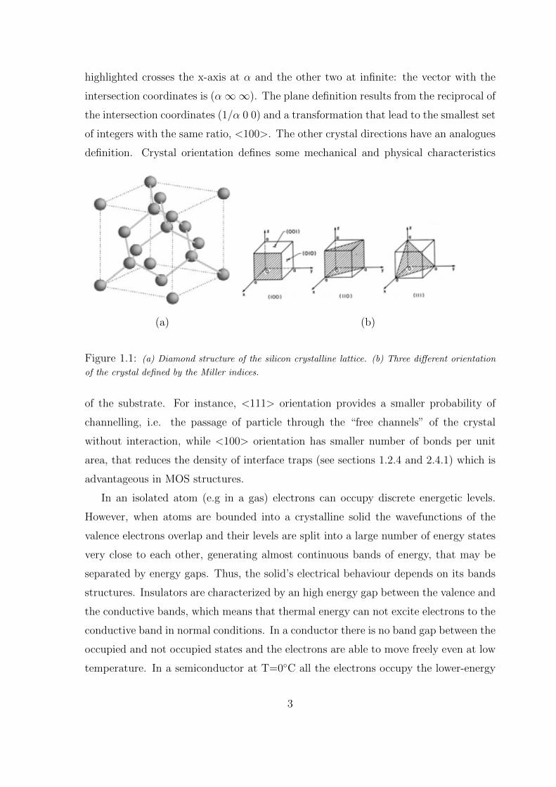
highlighted crosses the x-axis at α and the other two at infinite: the vector with the
intersection coordinates is (α ∞ ∞ ). The plane definition results from the reciprocal of
the intersection coordinates (1/α 0 0) and a transformation that lead to the smallest set
of integers with the same ratio, <100>. The other crystal directions have an analogues
definition. Crystal orientation defines some mechanical and physical characteristics
(a) (b)
Figure 1.1: (a) Diamond structure of the silicon crystalline lattice. (b) Three different orientation
of the crystal defined by the Miller indices.
of the substrate. For instance, <111> orientation provides a smaller probability of
channelling, i.e. the passage of particle through the “ free channels” of the crystal
without interaction, while <100> orientation has smaller number of bonds per unit
area, that reduces the density of interface traps (see sections 1.2.4 and 2.4.1) which is
advantageous in MOS structures.
In an isolated atom (e.g in a gas) electrons can occupy discrete energetic levels.
However, when atoms are bounded into a crystalline solid the wavefunctions of the
valence electrons overlap and their levels are split into a large number of energy states
very close to each other, generating almost continuous bands of energy, that may be
separated by energy gaps. Thus, the solid’ s electrical behaviour depends on its bands
structures. Insulators are characterized by an high energy gap between the valence and
the conductive bands, which means that thermal energy can not excite electrons to the
conductive band in normal conditions. In a conductor there is no band gap between the
occupied and not occupied states and the electrons are able to move freely even at low
temperature. In a semiconductor at T=0C all the electrons occupy the lower-energy
3

valence band. Due to the narrow energy gap, with increasing temperature some of the
electrons become thermally excited to the conduction band leaving unoccupied states
(holes) in the valence band. Both the free electrons in the conductive band and the
holes in the valence band can gain kinetic energy and momentum generating current
ow. The energy necessary to create an electron-hole pair depends on the band gap
width. The band structure of silicon is characterized by an energy gap of 1.12 eV. It
is high enough to allow silicon detectors work at room temperature (dierently from
Germanium, which energy gap is 0.66 eV), but low enough to ensure high signals
generation, i.e. high signal to noise ratio in proper conditions.
Intrinsic and doped silicon
The electrical properties of a semiconductor highly depend on the concentration
of impurities into its crystal lattice. A semiconductor is referred to as intrinsic if the
concentration of impurities is lower than the concentration of thermally generated free
carriers, that can be obtained by integrating over all the states of the valence and
conductive bands the density of states available with the probability of a state being
occupied by an electron (Fermi-Dirac distribution). Being n and p the concentration
of electrons and holes respectively, it gives:
n = Ncexp( Ec EF
kT
)and p = Nvexp
( EF Ev
kT
); (1.1)
where Nc and Nv are the density of the states in the conduction and valence band
respectively, k is the Boltzmann constant, T the temperature and EF the Fermi level,
the energy state with 50% chance of being occupied by an electron. In intrinsic silicon
the Fermi level is placed in the middle of the band gap (Ec-EF = EF -Ev) and carriers
concentration is the same for electrons and holes, n = p = ni, as they are produced in
pairs by thermal excitation. ni1010 cm3 at T=300 K, that can be compared with
copper in which ni1023 cm3 at the same temperature.
The presence of impurities in a semiconductor introduces new energy level inside
the band gap altering its behaviour. Silicon and the elements of group IV of the peri-
odic table have four valence electrons. Group V elements, such as Phosphorous, have 5
valence electrons and are referred to as donors. In the crystal, the extra electron is not
bound and occupy a level just below the edge of the conductive band. Thermal exci-
4

tation will let it pass to the conductive band leaving a xed positive ion in the crystal
lattice. If the concentration of donors Nd >> ni, then the electrons concentration will
be n=Nd and the material will be referred to as n-type doped. In this case the Fermi
level shifts towards the conductive band, due to the higher probability of occupation
of the states in the conductive band. Similarly, the group III elements, such as Boron,
having only 3 valence electrons, leave an empty level just above the valence band edge,
that will be occupy by an electron of the lattice (valence band). The result is a negative
xed ion in the lattice and an hole in the valence band. If Na >> ni, then the hole
concentration will be p=Na and the material referred to as p-type doped. In this case
the Fermi level shifts towards the valence band.
In general the carrier concentration is aected by both thermal generation and
electron-hole recombination, but in thermal equilibrium the rate of generation and
recombination will be equal and the carrier concentration will obey the action-mass
lay:
np = n2i (1.2)
Carrier transport and resistivity
Free electrons and holes move randomly into the crystal under thermal motion.
Two eects can cause a current ow of carriers: drift in an electric eld and diusion
from regions of high to region of low carrier concentration.
When an ionizing event occurs into the detector substrate, the free carriers created
must be collected by the electrodes in order to read and record the information. So,
an electric eld is established in the active volume by applying a potential between
the electrodes. Under the in uence of the electric eld E, electrons and holes are
accelerated along the eld lines and scatter frequently losing part of their momentum
in each collision. The resultant average drift velocity is given by:
vn = nE vp = pE (1.3)
where n and p are the mobility of electrons and holes respectively. In intrinsic
silicon, as well as in doped silicon up to a concentration 1016cm3, their values are
1350 cm2/Vs and 480 cm2/Vs. The higher the electric eld value, the higher the
velocity of the carrier and the faster the response of the detector. Although, for high
5
values of the electric eld the carrier velocity stop increasing assuming a saturation
value, due to the high rate of scattering.
The contribution of diusion to the net motion of carriers depends on the diusion
constant Dn,p = n,pkTq
(with q the charge of the electron) and on the carrier concen-
tration gradients rn and rp respectively. So, the overall current densities of electrons
and holes can be written as:
Jn = qnnE + qDnrn Jp = qppE + qDprp: (1.4)
The relationship between the current ow and the generation and recombination of
carriers is described by the carriers continuity equations. The rate of change in electrons
and holes concentration in an innitesimal volume is given by:
n
t= GR +
1
qr Jn
p
t= GR +
1
qr Jp; (1.5)
where G is the carrier generation rate and R is the recombination rate.
In carrier transport phenomena, mobility is a key parameter, that represent the
ability of an electron or hole to move inside a material under the in uence of an
electric eld. It can be also used to express the resistivity of the material:
=1
q(nn + pp)(1.6)
that can be simplied to = 1qµnNd
or = 1qµpNa
in n-type or p-type doped semicon-
ductors. At room temperature, resistivity of intrinsic silicon is 235 kcm, but it
fall o to values of the order of the 1-10 kcm in doped p- or n-type silicon.
To establish a high eld with a small quiescent current, the conductivity of the
absorber must be low. As an estimate, applying 30V across a 300 m thick absorber
yields an average eld of 103 V/cm, so the velocity of electrons is about 1.4106 cm/s and
it will take about 20 ns for an electron to traverse the detector thickness. Considering
the detector has a surface of 1 cm2 and a resistivity of 10 kcm. This means that its
total resistance is 300 , so the quiescent current owing in it will be of order 1 mA.
Since signal currents are typically of order A, resistance has to be reduced. A solution
is generating reverse-biased diode structures.
6

1.1.2 The p-n junction properties
The basic structure of a diode is a junction between n-type and p-type materials.
For example it can be obtained diusing sucient p-type impurities into a homoge-
neous region of n-type material so as to change the diusion region into a p-type
semiconductor. In this way a junction is formed at the p-n interface.
Figure 1.2: Schematic of the p-n junction in equilibrium. Charge distribution and electric eld inside
the depleted region are shown.
The dierence in the holes and electrons concentration gradients at the interface
causes diusion of holes from the p-type to the n-type region and of electrons from
the n-type to the p-type region. Due to this migration, a depleted zone is created
around the junction, with much lower carrier concentrations than in the bulk and
with uncompensated negatively-charged acceptors in the depleted p-type material and
positively-charged donors in the n-type material (see gure 1.2). The depletion region
extension is W = xp + xn, where Naxp = Ndxn. At the same time, this space charge
produces an electric eld, inside the depletion region, which cause carrier to drift in
the opposite direction of diusion current, reaching a state of equilibrium where the
net current is zero. the voltage dierence between the edges of the depletion region is
called the built-in potential which is normally of the order of 0.6 V to 0.8 V.
If we consider a p+-n (n+-p) junction, where the sign + indicates an high level of
dopants, the depletion region will extend practically only in the n-type (p-type) re-
7

gion, W xn,p and all the space charges in the depletion region will have the same
sign. Asymmetrical junction are normally created in semiconductor radiation detectors
where an external positive voltage Va is applied to the n-type region and a negative
voltage to the p-type. In this conguration Va has the same polarity (inverse polariza-
tion) of the built-in voltage, with the result of increasing the depletion region extension
in the less doped region. Let consider a p+-n junction, where the space charge has an
eective density Neff = Nd-Na. Using the Poisson equation:
d2V (x)
d2x=(x)
"; (1.7)
the electric eld can be written as:
E(x) =qNeff
"(xW ); (1.8)
with E(x = W ) = 0. A second integration with V (x = W ) = 0, gives:
V (x) = qNeff
2"(xW )2: (1.9)
So, the depletion width W is:
W (Va) =
√2"
q j Neff j(Vbi + Va); (1.10)
where " is the product of the electric constant "0 and the relative permittivity of the
semiconductor "r, which is 11.8 for silicon.
In a device with nite substrate thickness the full depletion width d is reach for a
value of the applied voltage Vdep. Since it act as an insulator layer, to the depleted
region is associated a capacitance per unit area that can be demonstrated to depend
quite only on the depletion width:
C ="
W=
√
e εNeff
2Vafor Va < Vdep
εSiε0d
for Va Vdep(1.11)
Vbi has been omitted because it is normally one order or two lower than Va.
In the inverse polarized p-n junction just a low leakage current ow through the
depleted region. In an ideal diode it is due to diusive motion of the few free carriers
that remain in the space charge region. But in a real device diusive current results
8

negligible compared to the current due to the generation of e h pairs by these
impurities or defects that introduce new energetic levels inside the band gap.
The generation current density is given by:
Jg = qniW
g; (1.12)
where g is the life time of the carriers generated due to the contribution of all the
levels in band gap:
g =(∑
i
1
i
)1: (1.13)
The value of Jg depends on the depletion width, i.e. on the voltage applied Jg / W /pVa and have a saturation value:
Jg =qnid
g: (1.14)
In the reality leakage current never saturate, because of supercial currents that in-
troduce more charges in the diode although in a small quantity with respect to the
charges generated by the defects. Finally, the current density value depends strongly
on the temperature of the structure:
Jg / T 2e∆EikT ; (1.15)
where Ei is the dierence in energy between the levels where the pair e h is
generated and the closest energy band: valence or conduction.
Now, considering the example at the end of the last section, generating a diode
structure in the silicon substrate and applying the same reverse-bias of 30V, we will
obtain a device with a leakage current 5 order of magnitude lower.
1.1.3 Basic diode detector
The simplest semiconductor radiation detector is a planar diode. Its structure is
shown in gure 1.3. It is fabricated on a silicon n-type (can be p-type) wafer slightly
(1012 cm3) doped with phosphorous ( can be boron) and hundreds of micron thick.
On the front and on the back surfaces, narrow, highly doped, regions (electrodes) are
created with thickness of the order of the micron and doping peak concentration of over
1018 cm3. A reverse bias is applied to the structure through metal contacts placed on
the highly doped regions.
9
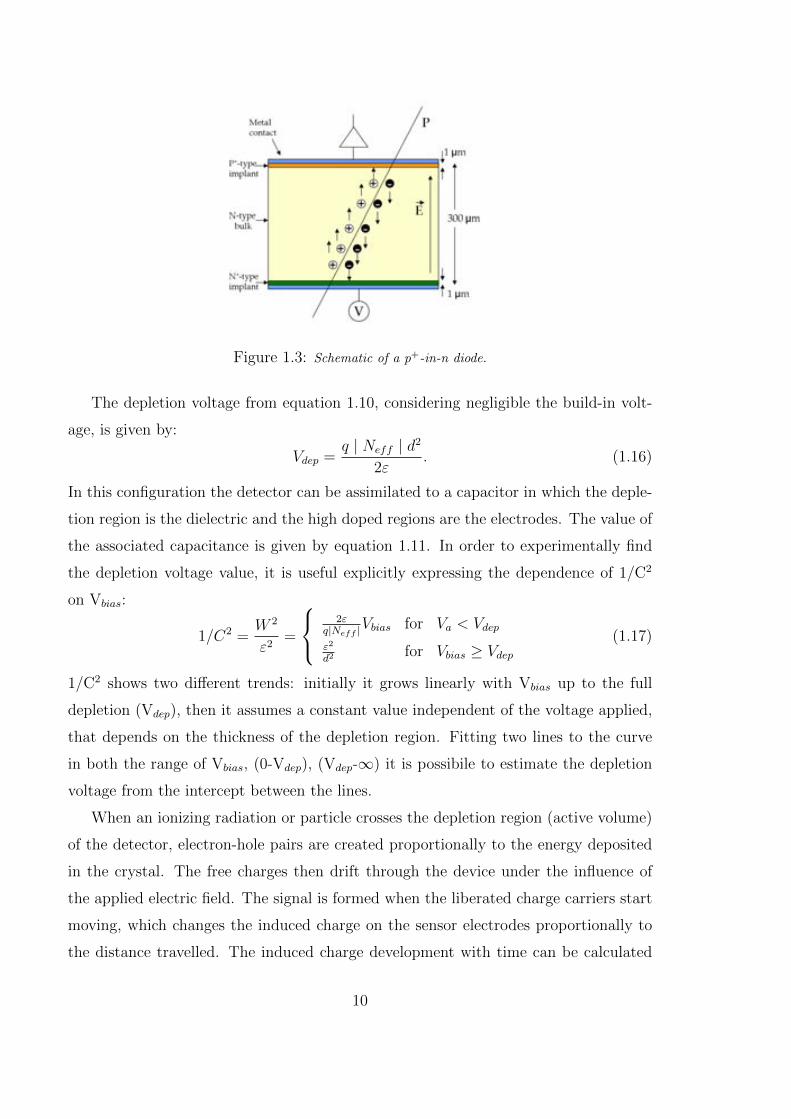
Figure 1.3: Schematic of a p+-in-n diode.
The depletion voltage from equation 1.10, considering negligible the build-in volt-
age, is given by:
Vdep =q j Neff j d2
2": (1.16)
In this conguration the detector can be assimilated to a capacitor in which the deple-
tion region is the dielectric and the high doped regions are the electrodes. The value of
the associated capacitance is given by equation 1.11. In order to experimentally nd
the depletion voltage value, it is useful explicitly expressing the dependence of 1/C2
on Vbias:
1=C2 =W 2
"2=
2εqjNeff j
Vbias for Va < Vdepε2
d2 for Vbias Vdep(1.17)
1/C2 shows two dierent trends: initially it grows linearly with Vbias up to the full
depletion (Vdep), then it assumes a constant value independent of the voltage applied,
that depends on the thickness of the depletion region. Fitting two lines to the curve
in both the range of Vbias, (0-Vdep), (Vdep-1) it is possibile to estimate the depletion
voltage from the intercept between the lines.
When an ionizing radiation or particle crosses the depletion region (active volume)
of the detector, electron-hole pairs are created proportionally to the energy deposited
in the crystal. The free charges then drift through the device under the in uence of
the applied electric eld. The signal is formed when the liberated charge carriers start
moving, which changes the induced charge on the sensor electrodes proportionally to
the distance travelled. The induced charge development with time can be calculated
10
using the Ramo's theorem [13], which demonstrates how it is due to the movement
of the charges elds inside the substrate, rather than by their collection. Actually,
although electrons are collected by the n-type electrode and holes by the p-type, the
signal induced in both electrodes is the same with opposite charge and results from
the superposition of the signals induced by both types of carriers. Then, as they
move towards opposite directions, the signals they induce in each electrode have the
same sign. The signal current begins when the carriers begin to move from the place
in which have been generated and nishes when all the charges are collected. The
collection time depends on the velocity of the carrier, i.e. on the electric eld strength
according to equation 1.3, t=x/E. Due to the dierence in the mobility of electrons
and holes (e 3h) electrons can be collected faster than holes. For instance, in
a eld of 2.5103 V/cm the electron velocity is 3.3106 cm/s, which means that in a
device 300 m thick electrons can be collected at least in 9 ns. In the same conditions
holes will be collected in 27 ns. A faster response can be obtained by increasing the
electric eld strength or reducing the electrodes distance. Electric eld can not be
increased indiscriminately. At elds >105 V/cm, electrons acquire sucient energy
to form secondary electron-hole pairs, ultimately leading to a destructive avalanche,
called \breakdown". On the other hand, reducing the electrodes distance in planar
detectors, will also reduce the active volume, causing a sensible decrease of the energy
loss by the radiation (particle), and an increase of the total capacitance of the detector,
that would aect the signal to noise ratio of the detector (see section 1.3.2).
Fixed the material and the geometry of the detector, the quantity and distribution
of the electron-hole pairs generated by ionising radiation will depend on the type of
radiation. In general, semiconductor detectors require a relatively low input of energy
to create an electron-hole pair, for example, the mean energy in silicon is 3.6 eV,
compared to 30 eV or so for gas detectors.
Photons will primarily interact with semiconductors by the photoelectric eect,
where the photon is absorbed in a single interaction and an electron gains its energy.
To generate an electron-hole pair, the photon energy must exceed the width of the
bandgap. So, for example, since silicon has 1.12eV bandgap it is transparent to infrared
light at wavelengths of beyond 1100nm (see chapter 2 and section 4.5). Photons of
visible light will produce a single electron-hole pair. X-ray photons, however, have
11

energies of thousands of electron volts, and will produce large numbers of electron-hole
pairs in a small spatial region where the photon was absorbed. The absorption of these
photons is probabilistic, so if we have a beam of X-rays the ux reaching a depth x
will be described by the Beer's law I=I0eαx, where is the absorption coecient.
Unlike a photon, a charged particle will undergo a series of Coulomb interactions
as it passes through silicon. These can be regarded as a series of collisions between
the particle and the electrons in the silicon. When a charged particle passes through
matter, its rate of energy loss with distance is given by the Bethe-Bloch formula [14],
assuming that the particle is not de ected by the collisions:
dE
dx= 2N0n
2emec
2Z
A
z2
2
[ln(2mec
2 22Wmax
I2
) 2 2
C
Z
](1.18)
where x is the path length in g/cm2, N0 is the Avogadro's number, re is the classic
radius of the electron, me is the electron mass, is the density of the medium, Z its
atomic number, A its atomic weight, z is the charge of the incident particle in units of e,
= v=c of the incident particle, = 1p1β2
, Wmax is the maximum energy transferred
in a single collision, I is the mean excitation potential, is a density correction and C is
a shell correction. At non-relativistic particle energies, the energy loss rate is inversely
proportional to the energy, through 2. Then the loss rate reach a minimum which
is quite independent of the material traversed. Particles with this energy are referred
to as Minimum Ionizing Particle (MIP) and are used as a reference in characterizing
detection eciency of detectors.
Since these interactions between charged particles and the semiconductor are sta-
tistical in nature, the total energy deposited by each particle will vary. However, in
thin layers of solid material as in semiconductor detectors for tracking applications, the
energy distribution produced over a large number of events is predictable, and follows
a Landau distribution.
1.2 Position sensing
The development of semiconductor position-sensitive detectors was made possible
by the adaptation of technologies used in Very Large Scale Integration (VLSI) micro-
electronics for the fabrication of silicon devices. In recent years, a very large variety
12
of detectors based on VLSI technology have been developed for many different appli-
cations in nuclear or particle physics tracking system as well as in space experiments.
However, in this section just the three main types of detector structures based on semi-
conductor technology will be introduced, as a background of the detectors presented
in the next chapters: microstrip detectors, pixel detectors and 3D detectors. Further
design considerations will be add at the end of the section.
1.2.1 Microstrip detectors
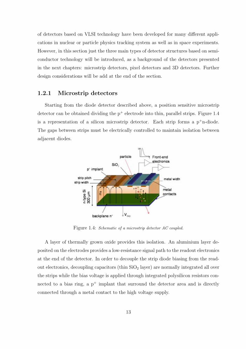
Starting from the diode detector described above, a position sensitive microstrip
detector can be obtained dividing the p+ electrode into thin, parallel strips. Figure 1.4
is a representation of a silicon microstrip detector. Each strip forms a p+n-diode.
The gaps between strips must be electrically controlled to maintain isolation between
adjacent diodes.
Figure 1.4: Schematic of a microstrip detector AC coupled.
A layer of thermally grown oxide provides this isolation. An aluminium layer de-
posited on the electrodes provides a low-resistance signal path to the readout electronics
at the end of the detector. In order to decouple the strip diode biasing from the read-
out electronics, decoupling capacitors (thin SiO2 layer) are normally integrated all over
the strips while the bias voltage is applied through integrated polysilicon resistors con-
nected to a bias ring, a p+ implant that surround the detector area and is directly
connected through a metal contact to the high voltage supply.
13
The electric eld lines remain parallel in the detector until near the surface, where
they bend along the surface and end on the electrode. The electrical segmentation
is determined by the electrode pitch (p), rather than the width. In a colliding-beam
experiment the strip pitch (centre-to-centre distance) is typically 25 - 100 m and the
maximum strip length (l) per sensor is limited by wafer size (10 - 15 cm for detector-
grade Si).
Considering each strip separately, the bulk capacitance associated to each one can
be expressed as :
Cd = "pl
d: (1.19)
Then, consecutive implants are linked to each other by \interstrip" capacitances which
value depends on the geometry of the strip (/ w=p, with w the strip width) and which
rule in the Signal to Noise ratio determination will be explained in section 1.3.2.
When a photon or a charged particle passes through the detector volume it induces
current signal to the electrodes, as discussed above. Segmentation of the electrode
in parallel strips makes the sensor sensitive to the position of the impinging radia-
tion/particle along the direction transversal to the strip length. A simple valuation of
the spatial resolution is given by the geometric resolution =p/p
12.
As explained in section 1.1.1, in addition to drift driven by the electric eld, the
charges are also subject to thermal diusion, which spreads the charge cloud trans-
versely with an rms width:
=p
2Dt =
√2kTt
q=
√2kTx
qE; (1.20)
which is the same for electrons and holes. So, in a device 300 m thick, with an
electric eld of 2.5103 V/cm, 6 m. Although it might seems to degrade the
obtainable position resolution, it can, in fact, improve it, increasing charge sharing
between electrodes. Actually, even if only one p+ electrode collects the charge, a signal
is induced also to its neighbours: a larger cloud of charges will involve more strips in the
induction process. Thus, when signals from each of the strips are read out separately,
the hit search can be done using cluster-nding algorithms (CFA), tailored according
to the geometry of the tracks [15] and a spatial resolution better than the geometric
resolution can be achieved. The range of charge interpolation can be extended by
introducing intermediate strips that are not connected to readout channels. The bias
14
resistors keep all strips at the same quiescent potential, but the time constant formed
by the bias resistance and the strip capacitance is made so large that the potential of a
floating strip can change individually in response to signal charge. The charge induced
on the “ floating” strips is then coupled capacitively to its neighbours.
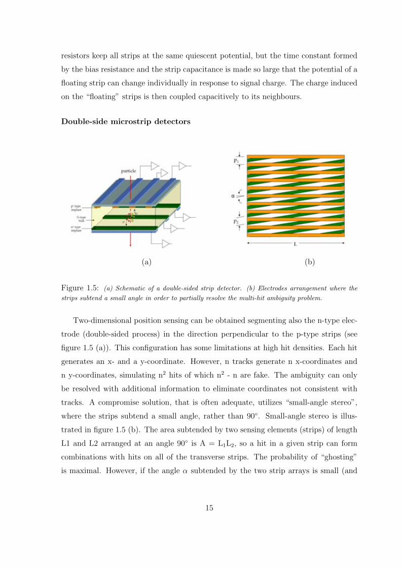
Double-side microstrip detectors
(a) (b)
Figure 1.5: (a) Schematic of a double-sided strip detector. (b) Electrodes arrangement where the
strips subtend a small angle in order to partially resolve the multi-hit ambiguity problem.
Two-dimensional position sensing can be obtained segmenting also the n-type elec-
trode (double-sided process) in the direction perpendicular to the p-type strips (see
figure 1.5 (a)). This configuration has some limitations at high hit densities. Each hit
generates an x- and a y-coordinate. However, n tracks generate n x-coordinates and
n y-coordinates, simulating n2 hits of which n2 - n are fake. The ambiguity can only
be resolved with additional information to eliminate coordinates not consistent with
tracks. A compromise solution, that is often adequate, utilizes “ small-angle stereo” ,
where the strips subtend a small angle, rather than 90. Small-angle stereo is illus-
trated in figure 1.5 (b). The area subtended by two sensing elements (strips) of length
L1 and L2 arranged at an angle 90 is A = L1L2, so a hit in a given strip can form
combinations with hits on all of the transverse strips. The probability of “ ghosting”
is maximal. However, if the angle α subtended by the two strip arrays is small (and
15
their lengths L are approximately equal), the capture area is:
A L2p2p1
tan + Lp2 (1.21)
The probability of multiple hits within the acceptance area, and hence the number
of ghosts, is reduced as is made smaller, but at the expense of resolution in the
longitudinal coordinate.
1.2.2 Pixel detectors
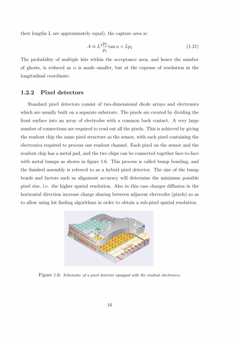
Standard pixel detectors consist of two-dimensional diode arrays and electronics
which are usually built on a separate substrate. The pixels are created by dividing the
front surface into an array of electrodes with a common back contact. A very large
number of connections are required to read out all the pixels. This is achieved by giving
the readout chip the same pixel structure as the sensor, with each pixel containing the
electronics required to process one readout channel. Each pixel on the sensor and the
readout chip has a metal pad, and the two chips can be connected together face-to-face
with metal bumps as shown in gure 1.6. This process is called bump bonding, and
the nished assembly is referred to as a hybrid pixel detector. The size of the bump
bonds and factors such as alignment accuracy will determine the minimum possible
pixel size, i.e. the higher spatial resolution. Also in this case charges diusion in the
horizontal direction increase charge sharing between adjacent electrodes (pixels) so as
to allow using hit nding algorithms in order to obtain a sub-pixel spatial resolution.
Figure 1.6: Schematic of a pixel detector equipped with the readout electronics.
16
1.2.3 3D detectors
A 3D detector is a variety of semiconductor diode detector where the p-i-n structure
is formed by columns of p- and n-type material (normally polysilicon) passing vertical
through the thickness of the substrate. The structure was proposed by S. Parker et al.
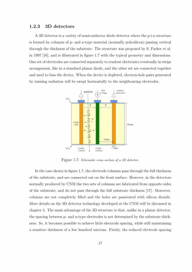
in 1997 [16], and is illustrated in figure 1.7 with the typical geometry and dimensions.
One set of electrodes are connected separately to readout electronics eventually in strips
arrangement, like in a standard planar diode, and the other set are connected together
and used to bias the device. When the device is depleted, electron-hole pairs generated
by ionising radiation will be swept horizontally to the neighbouring electrodes.
Figure 1.7: Schematic cross section of a 3D detector.
In the case shown in figure 1.7, the electrode columns pass through the full thickness
of the substrate, and are connected out on the front surface. However, in the detectors
normally produced by CNM the two sets of columns are fabricated from opposite sides
of the substrate, and do not pass through the full substrate thickness [17]. Moreover,
columns are not completely filled and the holes are passivated with silicon dioxide.
More details on the 3D detector technology developed at the CNM will be discussed in
chapter 4. The main advantage of the 3D structure is that, unlike in a planar detector,
the spacing between p- and n-type electrodes is not determined by the substrate thick-
ness. So, it becomes possible to achieve little electrode spacing, while still maintaining
a sensitive thickness of a few hundred microns. Firstly, the reduced electrode spacing
17
dramatically reduces the depletion voltage. As shown by equation 1.16, the depletion
voltage in a planar detector is proportional to the square of the electrode spacing. In
a 3D detector, the situation is more complicated. The depletion region around each
column will initially grow as a cylinder, nally reaching the other columns arranged
in a squared grid. In a rst cylindrical approximation the depletion voltage can be
written as:
Vdep =qNd
2"
(r2d
[ln(rdrc
) 0:5
]+ 0:5r2c
); (1.22)
where rd is radius of the depleted region and rc the radius of the column itself. So in
this case too, the depletion voltage depends on the square of the electrode spacing:
reducing this distance of a factor 10 would reduce the depletion voltage of the same
factor, as an example one can compare the results shown in section 2.5 for planar strip
detectors with substrate 300 m thick and resistivity in the range 5-7 kcm, with the
ones of section 4.4 where the characterization of 3D detectors with electrode spacing
56.6 m and processed on wafer with the same characteristic is presented. In the rst
case the depletion voltage has a value of about 40 V, while in the second case it is less
than 4 V. Similarly, the charge carriers collection time is determined by the collection
distance, which is dramatically reduced by the 3D structure, and the eld strength,
which will be higher in a 3D detector (at a given bias). So, the 3D detector achieves
fast charge collection, which is particularly important for radiation hardness of the
device.
Lifetime of silicon detectors in a severe radiation environment like accelerators de-
pends strongly upon their resistance to the radiation-induced damage. The main eect
of this damage consist in increasing the number of extra levels in the band gap that
can act as generation centres of e-h+ pairs or as traps for the free carriers, altering
the electrical behaviour of the substrate and the detector performance. The genera-
tion centres are responsible of an increase in the leakage current and in the depletion
voltage, while the traps will aect the charge collection of the carriers produced by
ionizing event.
Thanks to the very short distance between electrodes, the depletion voltage of 3D
detectors is substantially reduced with respect to planar detectors, and it should be
possible to fully deplete them even after high radiation doses (expected at HL-LHC)
as well as reducing the charge path to the electrodes, the number of trapped carriers
18

should be reduced, reducing charge collection degradation.
The 3D structure also reduces charge sharing between adjacent pixels [18]. Firstly,
the fast collection time means that the carriers have less opportunity to diuse out-
wards before being collected. Secondly, the 3D detector structure makes the carriers
drift horizontally to the columns, keeping them away from the pixel boundaries. In
contrast, in a planar detector the carriers drift vertically through the detector towards
the electrodes, and are free to diuse horizontally across the pixel boundaries. The
reduced charge sharing is not an advantage in every application. As mention in the
previous sections, charge sharing can be use to obtain a spatial resolution beyond the
pitch or pixel size. Other disadvantages of 3D detectors are, the dicult and expan-
sive fabrication process (see chapter 4.3), the inactive zone created by the electrode
columns themselves [19] and the high capacitance of the device. The electric eld will
be negligible within the doped polysilicon (due to the high carrier concentration and
high conductivity or to the empty/passivated volume inside them), and a signal will
only be produced by the small number of carriers which diuse out of the polysilicon
into the depletion region. Than, following the approximation to cylindrical depleted
region, the associated capacitance can be written as:
C =2"l
ln( rdrc
); (1.23)
that would be higher for smaller spacing of the electrodes like in the case of 3D detectors
compared with planar detectors. We will see how this fact represents a disadvantage
for what concern the electronic noise in section 1.3.2.
1.2.4 Further design considerations
In the previous sections, semiconductor detectors characteristics have been pre-
sented focusing the attention on the characteristic of the semiconductor substrate it-
self and on the dierent solutions one can achieve by choosing a proper geometry of
the electrodes. In this section, some important details concerning the active volume
boundaries will be discussed together with the designs and technologies developed to
improve the detector performance.
19
Charge accumulation at the silicon-oxide interface
As explained below, SiO2 is normally grown on the substrate surfaces to isolate
adjacent electrodes or to create decoupling capacitors between the implant electrodes
and the metal contacts. The resultant silicon-oxide interface is aected by dangling
bonds due to the crystal structure mismatch (see section 2.4.1) that act as traps for
the holes that slowly diuse through the oxide towards the substrate, creating positive
state charges. When electron-hole pairs are generated in silicon dioxide by ionising
radiation, the electrons have a high chance of diusing out of the oxide, whereas holes
which have low mobility, can be trapped, creating positive state charges. This charge
will attracts a layer of electrons to the silicon-oxide interface, which will aect the
electrical behaviour in this region. In a detector with p-type readout electrodes, a
higher eld region will be created where each p-type implant meets the electron layer,
ie at their boundaries. In a detector with n-type readout electrodes, the electron layer
will short the n-type implants together, causing unwanted signal sharing. In order
to avoid this eect, two common technologies have been developed [20] [21] , both
concerning the use of additional p-type dopants to generate a p-spay layer or a p-stop
implant. The p-spray is a uniform p+ layer across the entire surface (with much lower
concentration than the n+ electrodes), while the p-stop consists in strips or rings (see
chapter 4) of p+ implant between the n+ electrodes. Being the p-type implants close
to the n-type electrodes high-eld regions can be generated.
Edge eects and guard structures
A silicon wafer may contain many detector devices. So it must be diced to separate
the chips, and this is typically done using a diamond saw. The saw-cut edges will con-
tain many defects and dangling bonds. These defects make the edge more conductive
than the bulk material, and will also allow increase electron-hole pairs generation. If
the depletion region of the detector reaches the edge, then there can be a large cur-
rent ow from the edge to the junction and from one side to another of the bulk if
doped dierently, aecting the sensor behaviour. To prevent this, there is typically an
insensitive area around the chip, generally at least 100 m wide, containing guard ring
structures [22] that can stop currents from the edge and can dene the edge of the
active area of the detector. These structures are rings of doped implant of the same
20
type as the readout electrodes, in planar detectors, or rings of doped columns in 3D
detectors (see chapter 4). Generally, at least one of the guard rings will be biased.
Inactive areas are undesirable in detectors system like particle trackers, expecially in
these regions where high granularity and sensitivity is demanded. e.g. vertex detec-
tors. A mechanical solution is overlapping sensors modules where it is possible. As
an instance, in visible light and x-ray detectors overlapping does not help, as photons
are absorbed in the dead regions and lost for detection. A technological solution has
been proposed [23] for all these applications that need reducing the dead area around
the detectors. It concerns with using deep, reactive-ion etching in order to create deep
trenches all around the detector area and then doping properly and passivating the
edges obtaining active (electrodes) edges.
1.3 Signal processing
The readout electronic connected to the electrodes of a particle detector has many
dierent functions concerning basic signal processing on the data. The raw detector
signal is normally amplied and shaped through a lters system which tailors the overall
frequency response to optimize signal-to-noise ratio, while limiting the duration of the
signal pulse to accommodate the signal pulse rate. Pulse shaping determine both the
total noise and the peak signal amplitude at the output of the shaper. In this section
a brief analysis of the basic front-end electronics will be reported identifying the noise
sources in the circuit and the eects of short peaking time constant.
1.3.1 Basic front-end electronic
In gure 1.8 a diagram of a diode detector connected to the bias circuit and to
the basic front-end electronic is drawn. A capacitance Cd is associated to the sensor,
which is a good representation of most detectors. A bias voltage is applied through a
resistor Rb and the signal is coupled to the preamplier through a capacitor Cac. As
seen in previous sections, normally, both Rb and Cac are integrated in the microstrip
detector itself. The series resistance Rs represents the sum of all resistances present
in the input signal path, e.g. the electrode resistance and parasitic resistances in the
input transistor.
21

Figure 1.8: Schematic of the basic front-end electronics connected to a semiconductor detector.
As shown above, the passage of an ionizing particle through the detector volume
cause induced charges at the detector electrodes. This signal charge can be quite
small, about 4 fC (41015 C) in a typical high-energy tracking detector, so it must be
amplied. For this purpose, a charge sensitive preamplier is normally used, in which
almost all the current from the detector, ii(t), ows into the feedback capacitor Cf
charging it up. The output voltage is given (ideal preamplier, i.e. innite gain) by
Vout = Qi/Cf , where Qi is the total charge. Then, the capacitor will discharge through
an high resistor, represented by Rf . After the preamplier, additional ampliers can
also be used to increase the amplication.
The step-function signal at the output of the preamplier is then processed by
the shaper. In gure 1.8, a rst order CR-RC shaper is depicted. Although pulse
shapers normally have a more complicated structure, the CR-RC shaper contains the
essential features of all pulse shapers, reducing the frequencies spectrum of the signal
to a limited band. A high-pass lter (dierentiator) sets the duration of the pulse by
introducing a decay time constant d. Next a low-pass lter (integrator) increase the
rise time to limit the noise bandwidth. The overall frequency response is the product
of the individual frequency responses G(f) = Gint(f) Gdiff (f). Since in the Fourier
transform a product in the frequency domain is expressed in the time domain as the
convolution, the output pulse shape of the CR-RC shaper is the convolution of the
input signal with the time responses of the individual stages:
Vout(t) = Vi(t) gint(t) gdiff (t) =Qi
Cf
dd i
[et/τd et/τi
]; (1.24)
22
where d and i are the time constants of the dierentiator and the integrator respec-
tively. When d=i=
Vout(t) =Qi
Cf
t
et/τ ; (1.25)
is a good representation. The output pulse assumes its maximum at the peaking time
TP = . The noise performance of this simple shaper is only 36% worse than the
optimum lter. Thanks to its simplicity, the CR-RC shaper can be used for simple
estimation of the shaper performance.
1.3.2 Noise analysis
Reading out the signal produced by radiation/particle detectors, will always lead to
handle with electronic noise. It has many dierent sources, depending on the devices
involved in the readout electronic chain. In general, the amplitude distribution of
the noise is Gaussian, so noise uctuations superimposed on the signal also yield a
Gaussian distribution. Thus, by measuring the width of the amplitude spectrum of a
well-dened signal, one can determine the noise level.
Electronic noise places a lower bound on the detectable signal level and also deter-
mines the ability to distinguish signal levels or measure them precisely. In semiconduc-
tor position sensitive detectors, spatial resolution also depends on the Signal-to-Noise
ratio (S/N), thus improving this value, i.e. reducing the noise signal, is an important
goal that has to be taken into account since in the detector and the front-end electronic
design. Noise is due to many dierent eects.
Thermal noise, unavoidable at non-zero temperature, is due to the thermal agitation
of carriers in conductors and cause uctuation of the carrier velocity, it is associated
to the resistors and its spectral density versus frequency is:
dPndf
= 4kT; (1.26)
where k is the Boltzmann constant and T the absolute temperature.
On the other hand, shot noise generates time-dependent uctuations in the current
signal and is caused by the discreteness of the electron charge. It is typical of solid-
state devices based on p-n junctions. The spectral density of the current uctuations
can be expressed as:di2ndf
= i2n = 2eI; (1.27)
23

where I is the average current and e the electronic charge.
The noise spectrum becomes nonuniform whenever the uctuations are not purely
random in time, for example when carriers are trapped and then released with a time
constant . With an innite number of uniformly distributed time constants the spec-
tral power density assumes a pure 1/f distribution. A nite number of time constants
will reduce the 1/f distribution to a limited frequency range. The voltage spectral
distribution is given by:de2ndf
= e2n =Aff; (1.28)
where Af depends on the device.
Considering the front-end electronic described above it is possible to study the main
noise sources that aect the signal readout from a generic solid state detector.
Figure 1.9 represents the equivalent circuit of the detector front-end presented in
gure 1.8. The main noise sources inside and outside the detector are represented
by current (parallel component) or voltage en (series component) sources along the
circuit, with current or voltage spectral density in=di2n=df and en=de2n=df respectively.
Note that all the sources considered are placed before the preamplier and shaper
stage: actually, the noise signal act as any other electric signal, being amplied by the
correspondent circuital elements, so any other noise source after the preamplier input
is negligible.
Figure 1.9: Equivalent circuit for noise analysis of the detector connected to its front-end electronics.
The noise sources due to the detector concern with the leakage current (Id), the
bias resistor (Rb) and any resistive component in series (Rs) to the preamplier input,
e.g. the electrode resistance. The leakage current and the bias resistor components can
be modelled as current sources in parallel to the detector or the resistance respectively,
24

with spectral density:
i2nd = 2eId ; i2nb =4kT
Rb
: (1.29)
In order to simplify the analysis, current sources can be converted into voltage sources
in series to the input obtaining respectively:
e2nd =2eId
(wCd)2; j enb j2=
4kTRb
1 + (wRbCb)2: (1.30)
The series resistance component can include eects due to parasitic resistance at the
preamplier input and can be represented by a voltage source with spectral density:
e2ns = 4kTRs (1.31)
The noise due to the front-end electronics is mainly associated to the input tran-
sistor of the preamplier and can be represented by a current generator in parallel to
the input with current spectral density i2na = 2eIa and voltage generator, that lead to
two separated voltage generators in series with spectral density:
e2nai =i2na
(wCd)2and e2na = e2nw +
Aff: (1.32)
The contribute of these noise sources to the signal noise at the output of the shaper
can be obtained integrating the spectral density at the input of the preamplier e2ni =
e2nd+jenbj2+e2ns+e2nai+e
2na over all the frequency spectrum and considering the transfer
function A of the shaper:
Vno =0
∫ 1e2ni(f) jAf j2 df; (1.33)
with
jAj2 = 2d
(i + d)2 + (wid 1w
)2; (1.34)
that lead to:
V 2no =
1
4Cd
(4kT
Rb
+ 2eId + i2na
) 2di + d
+(4kTRs + e2na
) di(i + d)
+ Af 2d
2i + 2dlog(di
):
(1.35)
Normally, the noise is expressed in terms of Equivalent Noise Charge (ENC) which
represents the charge Qn injected in the detector volume that produces the same signal
25
read when no particle crosses the detector. The signal to noise ratio, then can be
written in terms of either the voltage signal or the charge:
S
N=Vso(TP )
Vnoor
S
N=Qs
Qn
; (1.36)
where Vso(TP ) is the peak value of the detected signal at the output of the shaper stage
and Qs the charge associated. Considering the CR-RC shaper with d=i= , TP = ,
the ENC due to the dierent noise sources can be demonstrated to be:
Q2n = Qs
Vno
Vno(TP )/
(2eId + 4kT
Rb+ 2eIa
) +
(4kTRs + e2na
) C2
τ+ 4AfC
2,
current noise voltage noise 1/f noise
(1.37)
where C is the total capacitance at the input of the preamplier, that is practically equal
to the detector capacitance Cd. The transfer function, then, introduces a dependence
to the peaking time . Higher peaking time would increase the current noise charge,
but decrease the voltage noise charge: the lower total noise would be achieved for a
value of that would make equal both the current and voltage components. 1/f noise
results independent of the constant time. For what concern the detector, its design
and technology should be developed accounting for reducing the series resistance, the
leakage current and the total capacitance, as well as obtaining an high bias resistance.
In this analysis a simple diode detector has been considered. The same results can be
achieved considering one channel of a position sensitive detector connected to the same
front-end electronics. For instance, lets consider one strip of a microstrip detector.
In this case the total capacitance seen by the preamplier input is not only the bulk
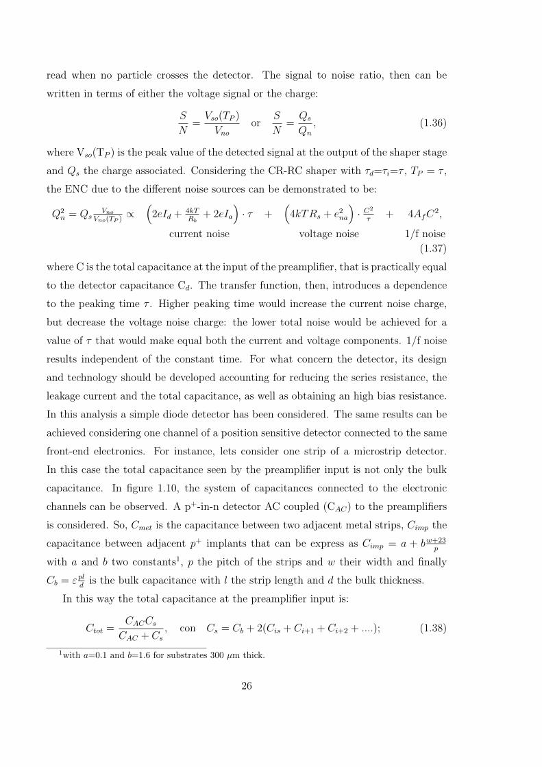
capacitance. In gure 1.10, the system of capacitances connected to the electronic
channels can be observed. A p+-in-n detector AC coupled (CAC) to the preampliers
is considered. So, Cmet is the capacitance between two adjacent metal strips, Cimp the
capacitance between adjacent p+ implants that can be express as Cimp = a + bw+23p
with a and b two constants1, p the pitch of the strips and w their width and nally
Cb = "pld
is the bulk capacitance with l the strip length and d the bulk thickness.
In this way the total capacitance at the preamplier input is:
Ctot =CACCsCAC + Cs
; con Cs = Cb + 2(Cis + Ci+1 + Ci+2 + ::::); (1.38)
1with a=0.1 and b=1.6 for substrates 300 m thick.
26
Figure 1.10: Schematic of the capacitances system connected to the readout electronics channels of a
microstrip detector . Cmet is the capacitance between two adjacent metal strips, Cimp the capacitance
between adjacent p+ implants, CAC is the coupling capacitance and Cb the bulk capacitance.
where Cs account for the contribution of interstrip capacitance between first neighbour-
ing strips (Cis), second neighbours (Ci+1), and so on. Since the coupling capacitance
is normally one or two orders of magnitude higher than the other capacitances and
p < d, the most important contribute to the total capacitance is given by the interstrip
capacitance.
Further considerations on noise will be presented in section 3.3.3, where a microstrip
detector with resistive coupling electrodes and read out at both sides of each strip will
be considered.
1.3.3 Ballistic deficit
As seen above, the peaking time of the shaper has a relevant influence on the total
noise charge. We will see in this section that another consideration in the choice of time
constants is the rise time of the input pulse applied to the shaper. Figure 1.8 shows
a δ signal at the output of the detector, converted in a step function with zero rise
time by the ideal preamplifier. This representation is convenient when characterizing
the pulse shaper alone. In reality the rise time is increased by the collection time of
the detector and the limited response time of the preamplifier. In many systems the
input rise time is much smaller than the shaping time, so the step input is an acceptable
approximation. However, when using short peaking times as in high-luminosity collider
27
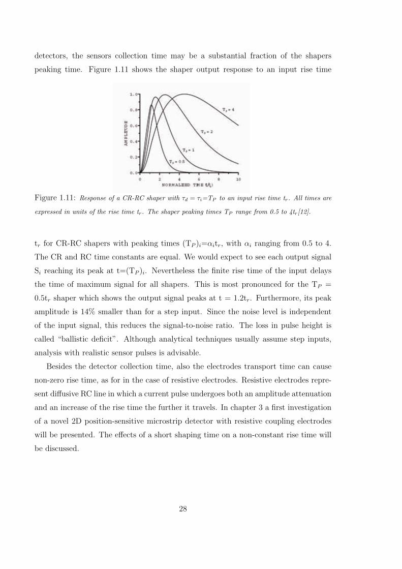
detectors, the sensors collection time may be a substantial fraction of the shapers
peaking time. Figure 1.11 shows the shaper output response to an input rise time
Figure 1.11: Response of a CR-RC shaper with τd = τi=TP to an input rise time tr. All times are
expressed in units of the rise time tr. The shaper peaking times TP range from 0.5 to 4tr[12].
tr for CR-RC shapers with peaking times (TP )i=αitr, with αi ranging from 0.5 to 4.
The CR and RC time constants are equal. We would expect to see each output signal
Si reaching its peak at t=(TP )i. Nevertheless the finite rise time of the input delays
the time of maximum signal for all shapers. This is most pronounced for the TP =
0.5tr shaper which shows the output signal peaks at t = 1.2tr. Furthermore, its peak
amplitude is 14% smaller than for a step input. Since the noise level is independent
of the input signal, this reduces the signal-to-noise ratio. The loss in pulse height is
called “ ballistic deficit” . Although analytical techniques usually assume step inputs,
analysis with realistic sensor pulses is advisable.
Besides the detector collection time, also the electrodes transport time can cause
non-zero rise time, as for in the case of resistive electrodes. Resistive electrodes repre-
sent diffusive RC line in which a current pulse undergoes both an amplitude attenuation
and an increase of the rise time the further it travels. In chapter 3 a first investigation
of a novel 2D position-sensitive microstrip detector with resistive coupling electrodes
will be presented. The effects of a short shaping time on a non-constant rise time will
be discussed.
28
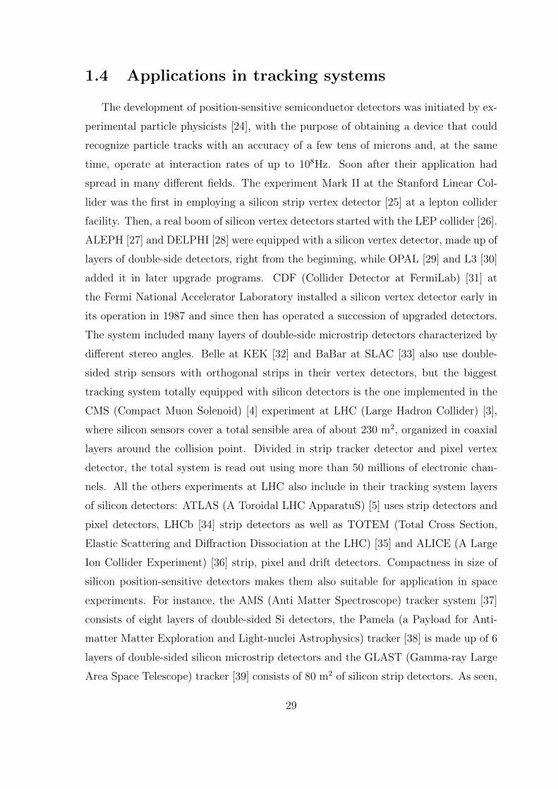
1.4 Applications in tracking systems
The development of position-sensitive semiconductor detectors was initiated by ex-
perimental particle physicists [24], with the purpose of obtaining a device that could
recognize particle tracks with an accuracy of a few tens of microns and, at the same
time, operate at interaction rates of up to 108Hz. Soon after their application had
spread in many dierent elds. The experiment Mark II at the Stanford Linear Col-
lider was the rst in employing a silicon strip vertex detector [25] at a lepton collider
facility. Then, a real boom of silicon vertex detectors started with the LEP collider [26].
ALEPH [27] and DELPHI [28] were equipped with a silicon vertex detector, made up of
layers of double-side detectors, right from the beginning, while OPAL [29] and L3 [30]
added it in later upgrade programs. CDF (Collider Detector at FermiLab) [31] at
the Fermi National Accelerator Laboratory installed a silicon vertex detector early in
its operation in 1987 and since then has operated a succession of upgraded detectors.
The system included many layers of double-side microstrip detectors characterized by
dierent stereo angles. Belle at KEK [32] and BaBar at SLAC [33] also use double-
sided strip sensors with orthogonal strips in their vertex detectors, but the biggest
tracking system totally equipped with silicon detectors is the one implemented in the
CMS (Compact Muon Solenoid) [4] experiment at LHC (Large Hadron Collider) [3],
where silicon sensors cover a total sensible area of about 230 m2, organized in coaxial
layers around the collision point. Divided in strip tracker detector and pixel vertex
detector, the total system is read out using more than 50 millions of electronic chan-
nels. All the others experiments at LHC also include in their tracking system layers
of silicon detectors: ATLAS (A Toroidal LHC ApparatuS) [5] uses strip detectors and
pixel detectors, LHCb [34] strip detectors as well as TOTEM (Total Cross Section,
Elastic Scattering and Diraction Dissociation at the LHC) [35] and ALICE (A Large
Ion Collider Experiment) [36] strip, pixel and drift detectors. Compactness in size of
silicon position-sensitive detectors makes them also suitable for application in space
experiments. For instance, the AMS (Anti Matter Spectroscope) tracker system [37]
consists of eight layers of double-sided Si detectors, the Pamela (a Payload for Anti-
matter Matter Exploration and Light-nuclei Astrophysics) tracker [38] is made up of 6
layers of double-sided silicon microstrip detectors and the GLAST (Gamma-ray Large
Area Space Telescope) tracker [39] consists of 80 m2 of silicon strip detectors. As seen,
29
dierent devices are used depending on many factors as the requirements of each exper-
iment and facility or the preference/experience of the designers of/in some particular
detector. For instance, a comparison between the tracker system of two general-purpose
experiments (CMS and ATLAS) at the same collider facility (LHC) is shown in g-
ure 1.12. The CMS tracker is totally equipped with silicon FZ detectors. It is divided
(a) (b)
Figure 1.12: (a) Schematic of the CMS tracking system (b) Schematic of the ATLAS tracking
system.
in a vertex detector and a tracker detector. The vertex detector is composed by pixel
detectors n+-in-n mounted on three barrels with radius 4:3 cm < r < 10:2 cm from the
collision point and two couple of end-cup disks at z = 34.5 cm and z = 46.5 cm
from the collision point. The tracking system is equipped with silicon strip detectors
with dierent pitch and thickness depending on the layer. The inner tracker consists
of four barrels and two couples of three end-cup disks with detectors 320 m thick and
pitch of 80 or 120 m. Some layers are covered with double-sided modules, obtained by
mounting two single-sided detectors face to face slightly tilted. The outermost barrel
includes 6 layers of microstrip detectors 500 m thick with pitch of 122 m or 183 m.
The tracker is then closed by two systems of end-cup disks (nine each one) where
sensors with thickness of 320 or 500 m and pitch between 81 m e 205 m are placed.
The ATLAS tracker adopted another strategy combining silicon DOFZ detectors
with transition radiation detectors. The vertex detector is still composed by silicon
pixel n+-in-n detectors arranged in three layers with radius 5:05 cm < r < 12:25 cm
30

from the collision point and three end-cup disks on each side between radii of 9 and 15
cm perpendicular to the beam. Outside the vertex detector, a Semiconductor Tracker
(SCT) composed of silicon strip detectors with pitch 80 m, is organized in four layers
with radius 29:9 cm < r < 51:4 cm and nine end-cup disks at each side. In he barrel
the same double-sided modules conguration as in CMS is used. In the outer region,
the tracker system is completed by a Transition Radiation Tracker (TRT), based on
the use of straw detectors.
For what concern the facilities, tracking and vertex detectors at lepton colliders have
to face simpler event topologies than at hadron colliders, free of the large backgrounds
inherent to hadron interactions. However the momenta of the particles of interest are
frequently low, so minimizing material in the active volume is crucial to limits multiple
scattering enhancing leptons id. Then, lepton colliders typically have a well-localized
interaction region, especially in linear colliders, allowing the tracker system to cover a
limited volume around it. On the other hand, experiments at hadron colliders must
deal with much higher interaction rates, which increases demands on rate capability.
Since most of the interactions are background, pattern recognition is crucial, which
increases the number of layers required for ecient track reconstruction. Furthermore,
the interaction region tends to be much more spread out in length, so the detectors
must be longer.
In general in a tracking system low mass is required to reduce multiple scattering,
low noise is requested to improve S/N, thus spatial resolution and momentum resolu-
tion, fast response need to face high interaction rate, low power is desirable to reduce
the costs and simplify the cooling system and nally, but not less important radiation
tolerance of the components is needed to ensure a long life of the experiment.
All these requirements can not be satised at the same time, but exploiting the sili-
con versatility, dierent compromises can be achieved. For example, in order to reduce
the system mass it is possible to thin the sensors bulk, that also improve radiation
hardness of the sensor and response velocity. However thinning the sensor also lead
to lower signal amplitude and higher capacitance, i.e. higher noise. A lower noise can
be achieved with higher power and high rate can be faced increasing granularity, that
would reduce interaction rate in each element (channel). 2D position sensitive detec-
tors are a solution to reduce the total mass of the system. Most recent studies, then,
31

demonstrate the high radiation hardness of 3D detectors, which are good candidate for
the CMS and ATLAS vertex detector upgrade for HL-LHC.
Finally, due to the multi-layers conguration of a silicon-based tracker, its precision
in track reconstruction, thus in momentum measurement, also depends on the stability
of the whole system, that can be achieved only implementing a proper alignment sys-
tem. As better explain in chapter 2 a laser alignment system (like that used by CMS
and AMS) provides good alignment without adding any other material to the detector.
1.4.1 Future accelerators
Looking at the future, two new big projects in high energy physics experiments call
for a continuous and deeper investigation of silicon position-sensitive detectors: the
upgrade of the LHC to HL-LHC and the building of the International Linear Collider
(ILC) [2]. The detector technologies developed in this thesis and presented in the next
chapters, nd their motivations in this context, ruled by improvement and innovation
urgency.
The LHC upgrade: HL-LHC
The Large Hadronic Collider (LHC) is a proton-proton collider installed at CERN [40]
(Geneva), in the 27 km tunnel (gure 1.13) that rstly housed LEP, the Large Elec-
tron Positron collider. In the tunnel the two protons beams are contained in two pipes
enclosed within superconductive magnets cooled by liquid helium. The beams are
composed of 2808 bunches containing 1011 protons each one and travel in opposite di-
rections colliding in four location along the tunnel with an centre-of-mass energy of 14
TeV. Currently LHC is working at a luminosity of 6.71030cm2s1, but it is designed
to reach a peak value of 1034cm2s1. For this reason the sensible components of the
four experiments installed in correspondence of the collision points have been designed
and fabricated so that properly work in a radiation environment characterized by a
uence of heavy particles of 1014neqcm2 at a distance of 20 cm from the interaction
point (IP) and of 1015neqcm2 at about 4 cm from the IP.
The upgrade of the LHC to High Luminosity-LHC (HL-LHC) envisaged for 2020,
foresee a luminosity increase from 1034 cm2s1 to 1035 cm2s1, that will require silicon
detectors in the central tracking detectors with unprecedented radiation tolerance.
32

Figure 1.13: The LHC accelerator and the beams injection system
Current radiation eld simulations for the general-purpose experiments ATLAS and
CMS foresee radiation levels of around 2.01016 neq/cm2 for the innermost pixel layers
and 1.01015 neq/cm2 for the innermost strip layers.
The luminosity can be expressed as:
L = fkBNbNb′
4n; (1.39)
where is the Lorents factor, f is the revolution frequency and the denominator is
basically the beam transverse area ( is the amplitude function) multilied by . Def-
inition and value of the other parameters are given in table 1.1 for both accelerator,
LHC and HL-LHC.
These HL-LHC uences exceed the LHC values by about an order of magnitude,
which means that with the HL-LHC, detectors in the innermost layers of the vertex
and tracking systems of ATLAS and CNM have to be replaced by a new generation of
highly radiation hard detectors.
CERN RD50 is an international collaboration of over 250 scientists from 47 insti-
tutes, working on semiconductor detectors to meet the challenges from high luminosity
colliders and hence high radiation environments [41]. The RD50 activities are grouped
into ve dierent research lines: defect and material characterisation, defect engineer-
ing, new structures, pad detector characterisation and full detector systems. A full
33
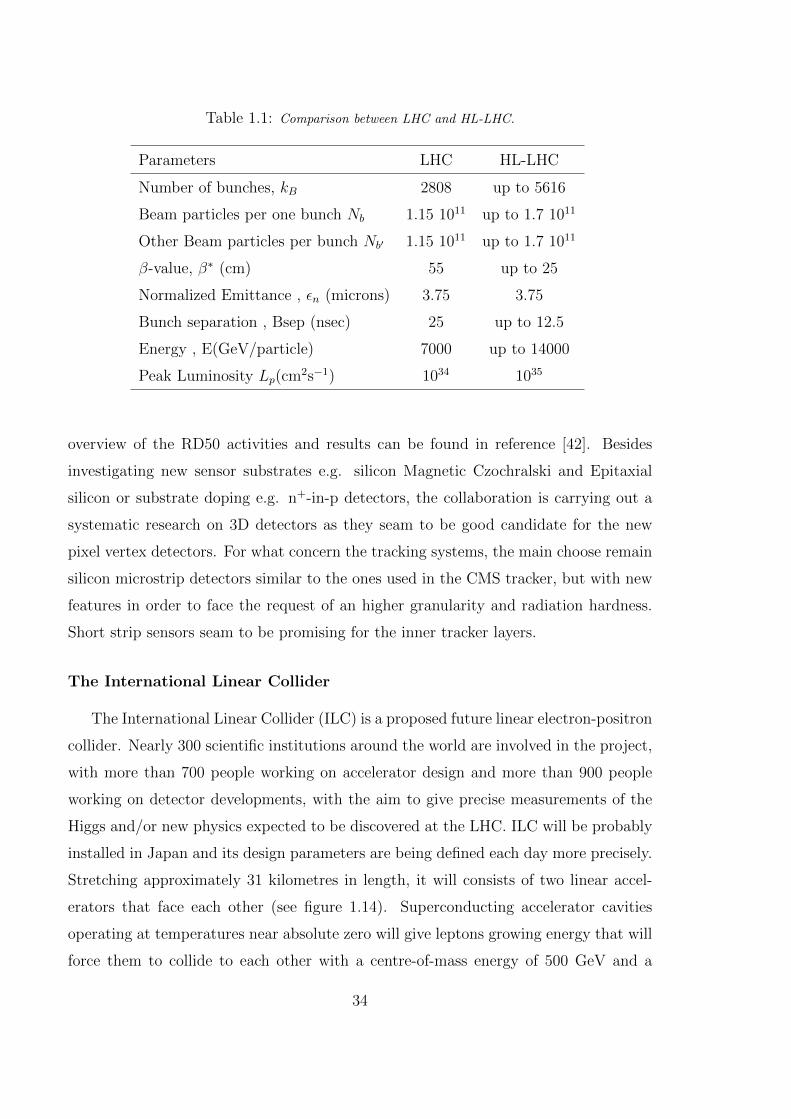
Table 1.1: Comparison between LHC and HL-LHC.
Parameters LHC HL-LHC
Number of bunches, kB 2808 up to 5616
Beam particles per one bunch Nb 1.15 1011 up to 1.7 1011
Other Beam particles per bunch Nb′ 1.15 1011 up to 1.7 1011
-value, (cm) 55 up to 25
Normalized Emittance , n (microns) 3.75 3.75
Bunch separation , Bsep (nsec) 25 up to 12.5
Energy , E(GeV/particle) 7000 up to 14000
Peak Luminosity Lp(cm2s1) 1034 1035
overview of the RD50 activities and results can be found in reference [42]. Besides
investigating new sensor substrates e.g. silicon Magnetic Czochralski and Epitaxial
silicon or substrate doping e.g. n+-in-p detectors, the collaboration is carrying out a
systematic research on 3D detectors as they seam to be good candidate for the new
pixel vertex detectors. For what concern the tracking systems, the main choose remain
silicon microstrip detectors similar to the ones used in the CMS tracker, but with new
features in order to face the request of an higher granularity and radiation hardness.
Short strip sensors seam to be promising for the inner tracker layers.
The International Linear Collider
The International Linear Collider (ILC) is a proposed future linear electron-positron
collider. Nearly 300 scientic institutions around the world are involved in the project,
with more than 700 people working on accelerator design and more than 900 people
working on detector developments, with the aim to give precise measurements of the
Higgs and/or new physics expected to be discovered at the LHC. ILC will be probably
installed in Japan and its design parameters are being dened each day more precisely.
Stretching approximately 31 kilometres in length, it will consists of two linear accel-
erators that face each other (see gure 1.14). Superconducting accelerator cavities
operating at temperatures near absolute zero will give leptons growing energy that will
force them to collide to each other with a centre-of-mass energy of 500 GeV and a
34
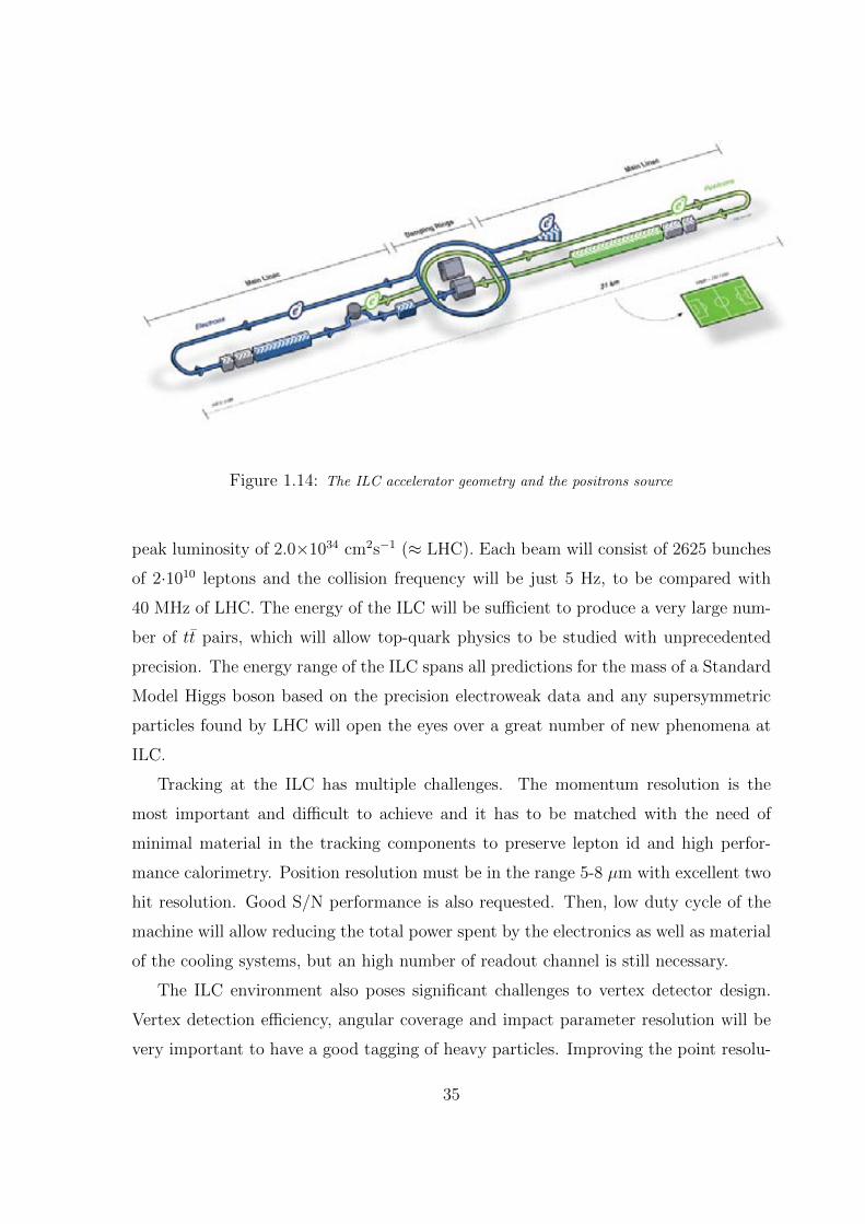
Figure 1.14: The ILC accelerator geometry and the positrons source
peak luminosity of 2.01034 cm2s1 ( LHC). Each beam will consist of 2625 bunches
of 21010 leptons and the collision frequency will be just 5 Hz, to be compared with
40 MHz of LHC. The energy of the ILC will be sucient to produce a very large num-
ber of tt pairs, which will allow top-quark physics to be studied with unprecedented
precision. The energy range of the ILC spans all predictions for the mass of a Standard
Model Higgs boson based on the precision electroweak data and any supersymmetric
particles found by LHC will open the eyes over a great number of new phenomena at
ILC.
Tracking at the ILC has multiple challenges. The momentum resolution is the
most important and dicult to achieve and it has to be matched with the need of
minimal material in the tracking components to preserve lepton id and high perfor-
mance calorimetry. Position resolution must be in the range 5-8 m with excellent two
hit resolution. Good S/N performance is also requested. Then, low duty cycle of the
machine will allow reducing the total power spent by the electronics as well as material
of the cooling systems, but an high number of readout channel is still necessary.
The ILC environment also poses signicant challenges to vertex detector design.
Vertex detection eciency, angular coverage and impact parameter resolution will be
very important to have a good tagging of heavy particles. Improving the point resolu-
35

tion per measurement and reducing the thickness of the detector sensors and supports
is then advisable. The low ILC radiation load admits a much wider selection of tech-
nologies than are possible at the LHC.
SiLC (Silicon tracking for the International Linear Collider) is a generic R&D col-
laboration aiming to develop the next generation of large area Silicon Trackers for the
ILC. The eort of the collaboration is focused on three main challenges: very high
precision on momentum (10 times better than in LEP), spatial resolution (better than
4 m, in certain regions, average 7-8 m) and large angle coverage. The request of low
material budget and low cost put constraints to whatever proposal. So, thin detectors
as well as 2D position-sensitive detectors are favoured and dierent solutions are being
investigated.
36

Chapter 2
IR Transparent detectors
In a semiconductor tracker detector system the precision in track reconstruction and
charged particles momentum measurements depends on the spatial resolution of the
sensing components as well as on the stability of the mechanical support on which the
sensors are mounted. In the experiments at accelerators as well as in space experiments,
many environmental disturbances cause stability of any supporting structure to be
aected at the micrometer level. In the rst case the detector is subject to local
temperature gradients (produced by operation and cooling of detectors) or humidity
changes while, in the second one, it undergoes vibrations during the transport before
deployment and rapid periodic changes in the thermal settings due to solar radiation
and cooling while in the shadow of Earth. Improving mechanical stability is currently
out of the technological reach, so other solutions have to be considered. The successful
experiences of the experiments AMS and CMS demonstrate that a Laser Alignment
System (LAS) is an elegant solution to achieve relative alignment between modules to
better than few microns. As shown in gure 2.1 it basically consists in a IR laser beam,
generated out of the tracker detectors nutshell, which traverses consecutive layers of
silicon microstrip sensors. The beam plays the role of an innite momentum track,
not bent by magnetic eld and even if silicon is almost transparent to IR light, its
absorption is enough to produce a signal that the sensors DAQ electronics can read
directly: beam position across several sensors can thus be monitored. Using the sensors
as their own alignment system, no mechanical transfer errors between ducial marks
and the modules are introduced, neither additional material or costs are needed, that
assure a minimum impact on the system integration.
37
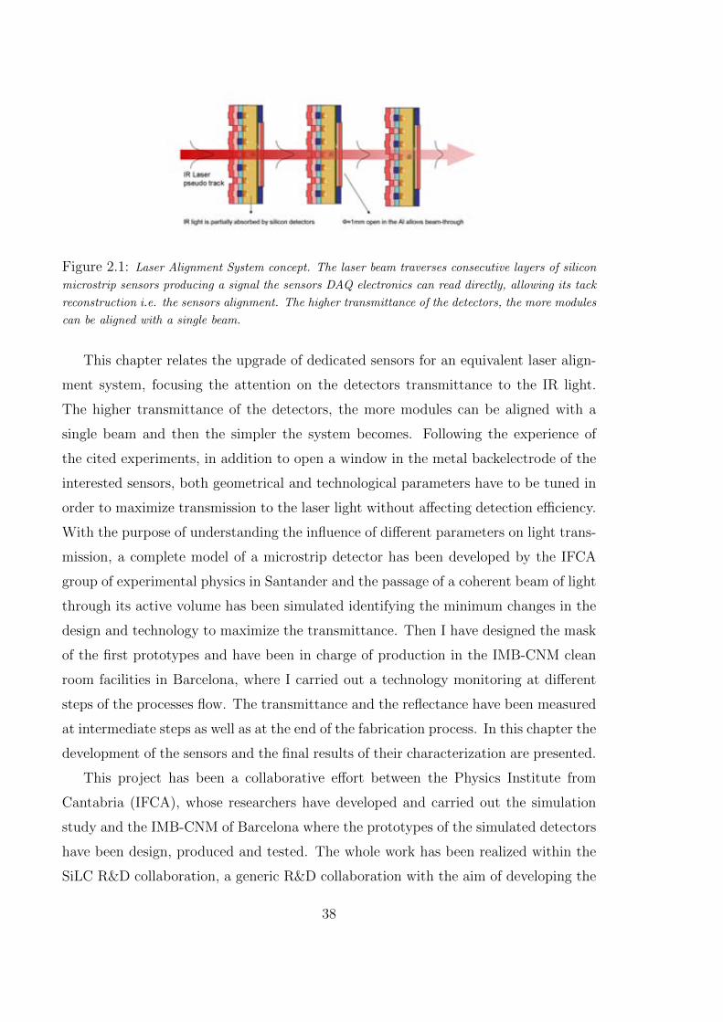
Figure 2.1: Laser Alignment System concept. The laser beam traverses consecutive layers of silicon
microstrip sensors producing a signal the sensors DAQ electronics can read directly, allowing its tack
reconstruction i.e. the sensors alignment. The higher transmittance of the detectors, the more modules
can be aligned with a single beam.
This chapter relates the upgrade of dedicated sensors for an equivalent laser align-
ment system, focusing the attention on the detectors transmittance to the IR light.
The higher transmittance of the detectors, the more modules can be aligned with a
single beam and then the simpler the system becomes. Following the experience of
the cited experiments, in addition to open a window in the metal backelectrode of the
interested sensors, both geometrical and technological parameters have to be tuned in
order to maximize transmission to the laser light without aecting detection eciency.
With the purpose of understanding the in uence of dierent parameters on light trans-
mission, a complete model of a microstrip detector has been developed by the IFCA
group of experimental physics in Santander and the passage of a coherent beam of light
through its active volume has been simulated identifying the minimum changes in the
design and technology to maximize the transmittance. Then I have designed the mask
of the rst prototypes and have been in charge of production in the IMB-CNM clean
room facilities in Barcelona, where I carried out a technology monitoring at dierent
steps of the processes ow. The transmittance and the re ectance have been measured
at intermediate steps as well as at the end of the fabrication process. In this chapter the
development of the sensors and the nal results of their characterization are presented.
This project has been a collaborative eort between the Physics Institute from
Cantabria (IFCA), whose researchers have developed and carried out the simulation
study and the IMB-CNM of Barcelona where the prototypes of the simulated detectors
have been design, produced and tested. The whole work has been realized within the
SiLC R&D collaboration, a generic R&D collaboration with the aim of developing the
38

next generation of large area Silicon trackers especially suited for performing very high
precision measurements in spatial position and momentum at the International Linear
Collider (ILC) machine (see section 1.4.1).
2.1 Laser alignment for tracking systems
Before introducing the new detectors, the choices adopted by the previous experi-
ments will be brie y presented in this section together with the results obtained.
2.1.1 AMS Tracker Alignment System
The AMS tracker consists of 8 layers of double-sided 300 m thick Si strip detectors.
The strip (readout) pitch is 27.5 (110) m for the p-type side and 104 (208) m for the
n-type side. The alignment system is equipped with 210 pairs of beams at = 1082 nm
crossing selected sensors in each layer. For these sensors windows in the aluminium
backelectrode has been created in order to allow the beams pass through the whole
detector towards the next one. Then, the readout strip metallizationzation has been
narrowed to 10 m width and removed from the implants not used for the readout.
Passivation layers of SiO2 and Si3O4 have been deposited on both sides of the detectors
as Anti-Re ection Coating (ARC). The nal transmittance achieved for these devices
is above 50%.
2.1.2 CMS Tracker Alignment System
CMS tracker components vary depending on the region of the multi-layer system
they occupy: they are single-sided p+-on-n strip detectors whose thickness range be-
tween 320 and 500 m and strip pitch between 80 and 205 m. Strip width/pitch is a
constant parameter for every detector, including the ones dedicated for the alignment
system, whose metallizations have not been narrowed. In this case, the only modi-
cation made to these detectors was opening a circular window in the backside ohmic
contact and coating it with an ARC made of selected thickness of Ta2O5 and SiO2. The
system employs a total of 40 laser diodes working at = 10753 nm. The resultant
transmittance at the AMS working wavelength is 21%.
39
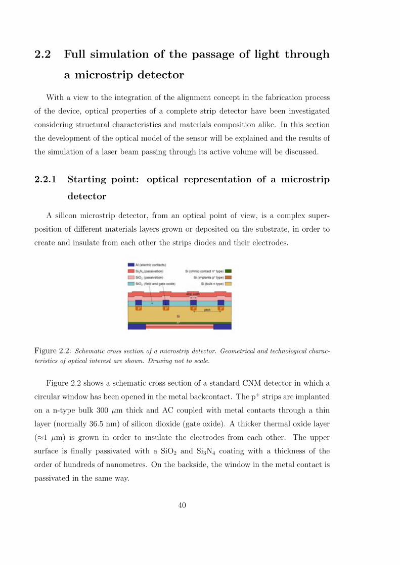
2.2 Full simulation of the passage of light through
a microstrip detector
With a view to the integration of the alignment concept in the fabrication process
of the device, optical properties of a complete strip detector have been investigated
considering structural characteristics and materials composition alike. In this section
the development of the optical model of the sensor will be explained and the results of
the simulation of a laser beam passing through its active volume will be discussed.
2.2.1 Starting point: optical representation of a microstrip
detector
A silicon microstrip detector, from an optical point of view, is a complex super-
position of dierent materials layers grown or deposited on the substrate, in order to
create and insulate from each other the strips diodes and their electrodes.
Figure 2.2: Schematic cross section of a microstrip detector. Geometrical and technological charac-
teristics of optical interest are shown. Drawing not to scale.
Figure 2.2 shows a schematic cross section of a standard CNM detector in which a
circular window has been opened in the metal backcontact. The p+ strips are implanted
on a n-type bulk 300 m thick and AC coupled with metal contacts through a thin
layer (normally 36.5 nm) of silicon dioxide (gate oxide). A thicker thermal oxide layer
(1 m) is grown in order to insulate the electrodes from each other. The upper
surface is nally passivated with a SiO2 and Si3N4 coating with a thickness of the
order of hundreds of nanometres. On the backside, the window in the metal contact is
passivated in the same way.
40
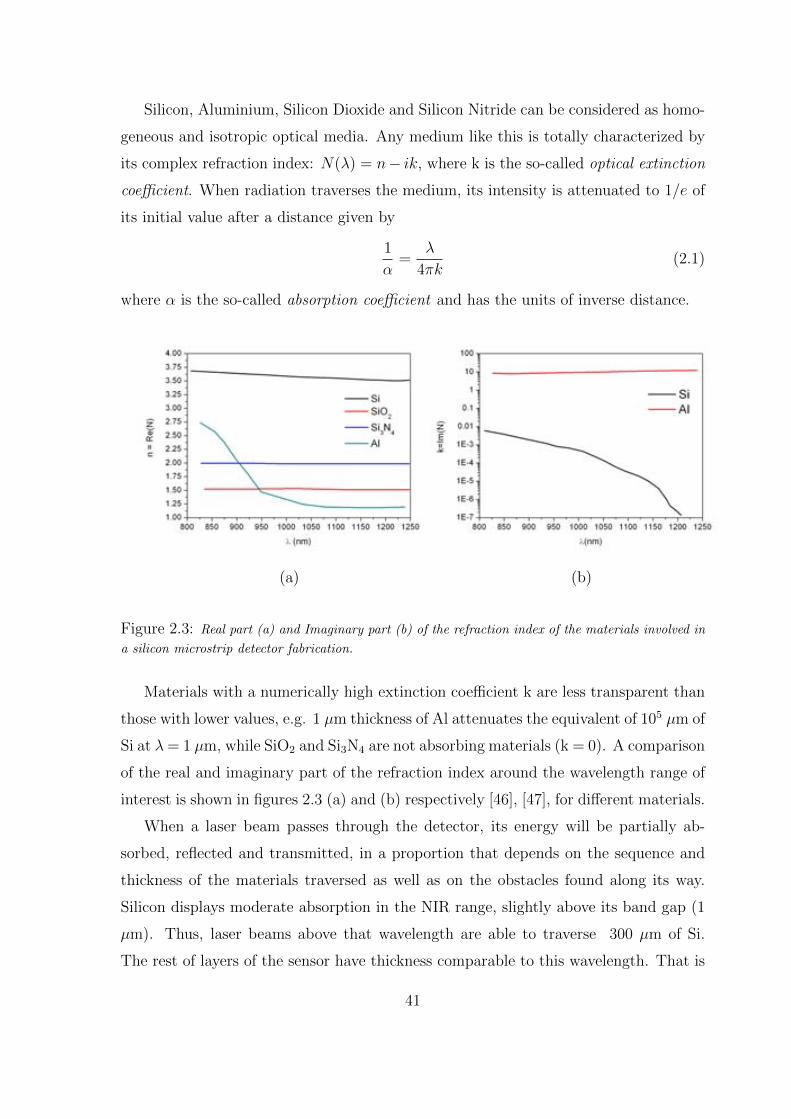
Silicon, Aluminium, Silicon Dioxide and Silicon Nitride can be considered as homo-
geneous and isotropic optical media. Any medium like this is totally characterized by
its complex refraction index: N() = n ik, where k is the so-called optical extinction
coecient. When radiation traverses the medium, its intensity is attenuated to 1=e of
its initial value after a distance given by
1
=
4k(2.1)
where is the so-called absorption coecient and has the units of inverse distance.
(a) (b)
Figure 2.3: Real part (a) and Imaginary part (b) of the refraction index of the materials involved in
a silicon microstrip detector fabrication.
Materials with a numerically high extinction coecient k are less transparent than
those with lower values, e.g. 1 m thickness of Al attenuates the equivalent of 105 m of
Si at = 1 m, while SiO2 and Si3N4 are not absorbing materials (k = 0). A comparison
of the real and imaginary part of the refraction index around the wavelength range of
interest is shown in gures 2.3 (a) and (b) respectively [46], [47], for dierent materials.
When a laser beam passes through the detector, its energy will be partially ab-
sorbed, re ected and transmitted, in a proportion that depends on the sequence and
thickness of the materials traversed as well as on the obstacles found along its way.
Silicon displays moderate absorption in the NIR range, slightly above its band gap (1
m). Thus, laser beams above that wavelength are able to traverse 300 m of Si.
The rest of layers of the sensor have thickness comparable to this wavelength. That is
41
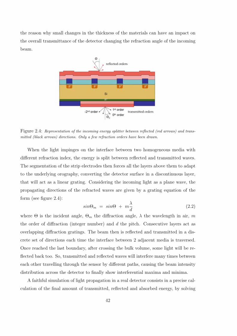
the reason why small changes in the thickness of the materials can have an impact on
the overall transmittance of the detector changing the refraction angle of the incoming
beam.
Figure 2.4: Representation of the incoming energy splitter between re ected (red arrows) and trans-
mitted (black arrows) directions. Only a few refraction orders have been drawn.
When the light impinges on the interface between two homogeneous media with
dierent refraction index, the energy is split between re ected and transmitted waves.
The segmentation of the strip electrodes then forces all the layers above them to adapt
to the underlying orography, converting the detector surface in a discontinuous layer,
that will act as a linear grating. Considering the incoming light as a plane wave, the
propagating directions of the refracted waves are given by a grating equation of the
form (see gure 2.4):
sinm = sin + m
d(2.2)
where is the incident angle, m the diraction angle, the wavelength in air, m
the order of diraction (integer number) and d the pitch. Consecutive layers act as
overlapping diraction gratings. The beam then is re ected and transmitted in a dis-
crete set of directions each time the interface between 2 adjacent media is traversed.
Once reached the last boundary, after crossing the bulk volume, some light will be re-
ected back too. So, transmitted and re ected waves will interfere many times between
each other travelling through the sensor by dierent paths, causing the beam intensity
distribution across the detector to nally show interferential maxima and minima.
A faithful simulation of light propagation in a real detector consists in a precise cal-
culation of the nal amount of transmitted, re ected and absorbed energy, by solving
42

Maxwell's equations in the input, grating and output regions fullling the boundary
conditions for the tangential electric and magnetic eld components at the respec-
tive interfaces [43]. Two open source programs, from the photonics group of the
Department of Information Technology at Ghent University (Belgium), RODIS and
CAMFR [44] [45], have been employed for this purpose.
At this rst stage, optical characteristics of the materials involved in the sensor
schematics have been taken from literature: refractive index of SiO2, Si3O4, Al from
reference [46]; precision measurements of Silicon within the absorption gap from refer-
ence [47].
Figure 2.5: Picture of the wafers used to crosscheck doped silicon properties dened in literature and
the simulation tool. Left to right , top to bottom: a reference wafer without doping implants, wafer
with increasing doping concentration. Dierent thickness of SiO2 and Si3N4 are deposited on the four
quadrants of the wafers.
Optical properties of doped Si are reported to be very dierent from intrinsic Si (see
43

for instance [48]). In order to crosscheck these measurements and validate the simula-
tion tool, many wafers produced at CNM within the GICSERV access framework have
been used [49] [50]. Four double-side polished wafers have been used to implant on one
surface boron atoms with increasing doping concentrations and total thickness of 1 m.
The wafers have been measured with a grating spectrometer (1.2 nm spectral resolu-
tion) operating in the wavelength range 950-1150 nm. Contrary to what was expected,
the same light transmittance has been measured from all the wafers regardless of dop-
ing concentration. The dierent thicknesses of SiO2 and Si3N4 have been deposited on
the four quadrants of each wafer in order to study their optical properties. A picture
of all the wafers used for this test is shown in gure 2.5. Simulation of the diraction
eects due to the metal strips has been tested by means of known structures of metal
strips 1 m thick, 30 m wide and with a pitch of 80 m deposited on a thin lm of
silicon dioxide (36.5 nm) grown on a silicon bulk (28515) m thick (bottom wafer in
gure 2.5). The simulation has been carried out keeping 40 diraction orders in the
calculation and assuming a roughness 45 nm for the aluminium (measured by an
Atomic Force Microscopy (AFM)), that accounts for decreasing of specular re ectance,
(see section 2.4.2).
2.2.2 Preliminary optimization of the design
The full optical tool presented in section 2.2.1 has been used to study the key
parameters that determine the transmittance of the detector to the IR light. Both
layout parameters and material layers thickness have been taken into account.
At rst, the thicknesses of the material layers were xed to the ones of the standard
CNM fabrication process [53] and the attention was focused on the eects of the grating
parameters.
Figure 2.6 shows how the simulated transmittance changes as a function of the
pitch and of the (metal) strip-width of the sensor: the transmittance increases for
larger strip pitches at a xed value of the strip width and for a smaller strip width at a
xed pitch value. For a baseline pitch of 50 m (xed by the SiLC Collaboration for the
experiment at the ILC) a metal strip width 5 m (strip-width/pitch ratio 10%)
optimizes the transmittance.
In a second time, these geometrical parameters were xed and the same structure
44
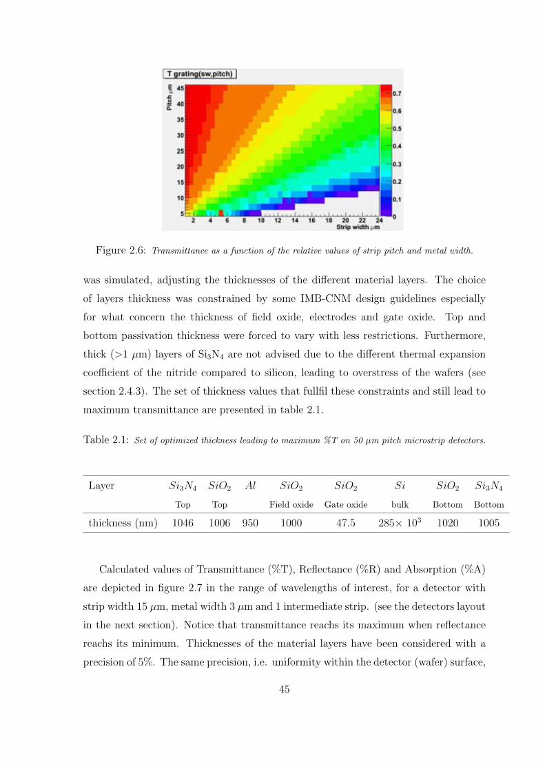
Figure 2.6: Transmittance as a function of the relative values of strip pitch and metal width.
was simulated, adjusting the thicknesses of the dierent material layers. The choice
of layers thickness was constrained by some IMB-CNM design guidelines especially
for what concern the thickness of eld oxide, electrodes and gate oxide. Top and
bottom passivation thickness were forced to vary with less restrictions. Furthermore,
thick (>1 m) layers of Si3N4 are not advised due to the dierent thermal expansion
coecient of the nitride compared to silicon, leading to overstress of the wafers (see
section 2.4.3). The set of thickness values that fulll these constraints and still lead to
maximum transmittance are presented in table 2.1.
Table 2.1: Set of optimized thickness leading to maximum %T on 50 m pitch microstrip detectors.
Layer Si3N4 SiO2 Al SiO2 SiO2 Si SiO2 Si3N4
Top Top Field oxide Gate oxide bulk Bottom Bottom
thickness (nm) 1046 1006 950 1000 47.5 285 103 1020 1005
Calculated values of Transmittance (%T), Re ectance (%R) and Absorption (%A)
are depicted in gure 2.7 in the range of wavelengths of interest, for a detector with
strip width 15 m, metal width 3 m and 1 intermediate strip. (see the detectors layout
in the next section). Notice that transmittance reachs its maximum when re ectance
reachs its minimum. Thicknesses of the material layers have been considered with a
precision of 5%. The same precision, i.e. uniformity within the detector (wafer) surface,
45

Figure 2.7: Values of Transmittance (%T) (black line), Re ectance (%R) (red line)and Absorption
(%A) (green line) calculated in the range of wavelengths of interest. Transmittance has been maximized
(re ectance minimized) for = 1085 nm (vertival line) setting the thickness of the dierent materials
to the values listed in table 2.1.
is thus requested to the fabrication process used to grow or deposit the real materials to
garantee the reproducibility of the sensor optical characteristics in a bunch of wafers.
2.3 Layout of the detectors
The layout for the rst prototype detectors has been designed respecting simulation
hints. Mask design includes twelve baby sensors equipped with 256 readout strips with
a pitch of 50 m. The active area is about 1.2 1.5 cm2 surrounded by nine guard
rings. A circular window (1 cm diameter) has been opened in the aluminium backplane
to allow the laser beam passing through. The width of the aluminium electrodes and
p+-implants were varied from sensor to sensor within the wafer to study the dependence
of transmittance and electrical behaviours on these layout parameters. Figure 2.8 shows
the arrangement of sensors in the wafer and their characteristics.
The layout of the 6 sensors in the upper half (S1-S6) includes intermediate strips
without aluminium coating (one within two readout strips), that have the function of
increasing the spatial resolution by means of capacitive charge division.
For instance, details of the layout of sensor S4 and S6 can be seen in gure 2.9 (a)
and (b) respectively. In both cases, superposition of mask levels (better described in
the next section) are depicted: among all, one can recognize the metal coating of strips
46

(a) (b)
Figure 2.8: Mask design for the sensors production (a). Layout specications are listed in the table
on the right (b). Diode structures D1, D2 are included in the mask as well as optical test structures
(TS1-TS4) and other electrical test structures. Sensors A and B are described in chapter 3.
(a) (b)
Figure 2.9: Details of the mask design of sensor S4 (a) and S6 (b). On the left, the implant (readout)
pitch and implant (metal coating) width are indicated while on the right the design of bias resistance
is shown.
and bias (guard) ring colored in blue, the p+ implants drawn in yellow (borders and
dots inside), and the polysilicon bias resistors in red. On the left, dimensions of interest
are indicated like the implants (readout) pitch (25 m, 50 m) and the implants and
metal coating width (15 m, 5 m). On the right, the attention is focused on the
bias resistors. They have been designed adapting their geometry to the orography
47
of silicon dioxide on which polysilicon is deposited (see drawing within the gure),
aiming a proper value of the resistance while keeping limited their total length and
respecting photolithography precision limits for microelectronic processes set to 3m
(see section 2.4.5). The intermediate strips are connected to the bias ring on the other
end, in order to further preserve resistances from shorting.
Referring to gure 2.8 (a), one leftmost and one rightmost structures in the top
row (Diode 1 and 2) are control diodes. Unpatterned optical test structures (OTS1 to
OTS4) are placed in rows second and third. These structures, described in section 2.6,
allow to extract and monitor optical constants (refraction index and thickness) of the
materials employed in the production.
Finally, these wafers also include test structures designed by HEPHY-Vienna [51] for
CMS experiment (that can be used for indirect measurements of the detectors electrical
parameters) and prototype sensors with polysilicon strips to investigate tracking by
charge division that will be the subject of chapter 3.
2.4 Fabrication process and technology monitoring
Silicon detectors fabrication processing uses the same techniques and hardwares
developed in the last fty years by the semiconductor industry. The IMB-CNM clean
room facility with a surface of 1500 m2 has the capability of fabricating integrated
devices with CMOS processes and includes microsystem-specic and nanofabrication
processes.
The detectors described in this chapter have been processed on oat-zone n-type
silicon wafers by Topsil [52] with < 100 > crystal orientation. Their nominal thickness
is 285 15 m and resistivity between 5 and 7 kcm.
As mention in section 2.2.1, the nished device results from the superposition of
dierent grown or deposited material layers on which structures are dened by pho-
tolithography processes. Photolithography is the patterning process that transfers the
design layout from the mask to the photoresist on the wafer surface. It is the most
crucial process step, since the device design is transferred to the wafer by either etch or
implantation through the pattern dened on the photoresist. It requires high resolu-
tion, high sensitivity, low defect density and precise alignment between dierent level of
48
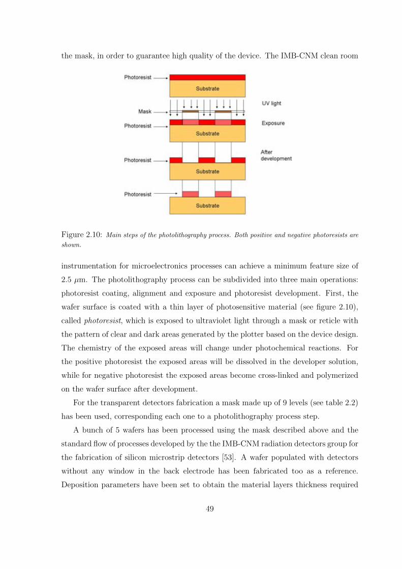
the mask, in order to guarantee high quality of the device. The IMB-CNM clean room
Figure 2.10: Main steps of the photolithography process. Both positive and negative photoresists are
shown.
instrumentation for microelectronics processes can achieve a minimum feature size of
2.5 m. The photolithography process can be subdivided into three main operations:
photoresist coating, alignment and exposure and photoresist development. First, the
wafer surface is coated with a thin layer of photosensitive material (see gure 2.10),
called photoresist, which is exposed to ultraviolet light through a mask or reticle with
the pattern of clear and dark areas generated by the plotter based on the device design.
The chemistry of the exposed areas will change under photochemical reactions. For
the positive photoresist the exposed areas will be dissolved in the developer solution,
while for negative photoresist the exposed areas become cross-linked and polymerized
on the wafer surface after development.
For the transparent detectors fabrication a mask made up of 9 levels (see table 2.2)
has been used, corresponding each one to a photolithography process step.
A bunch of 5 wafers has been processed using the mask described above and the
standard ow of processes developed by the the IMB-CNM radiation detectors group for
the fabrication of silicon microstrip detectors [53]. A wafer populated with detectors
without any window in the back electrode has been fabricated too as a reference.
Deposition parameters have been set to obtain the material layers thickness required
49
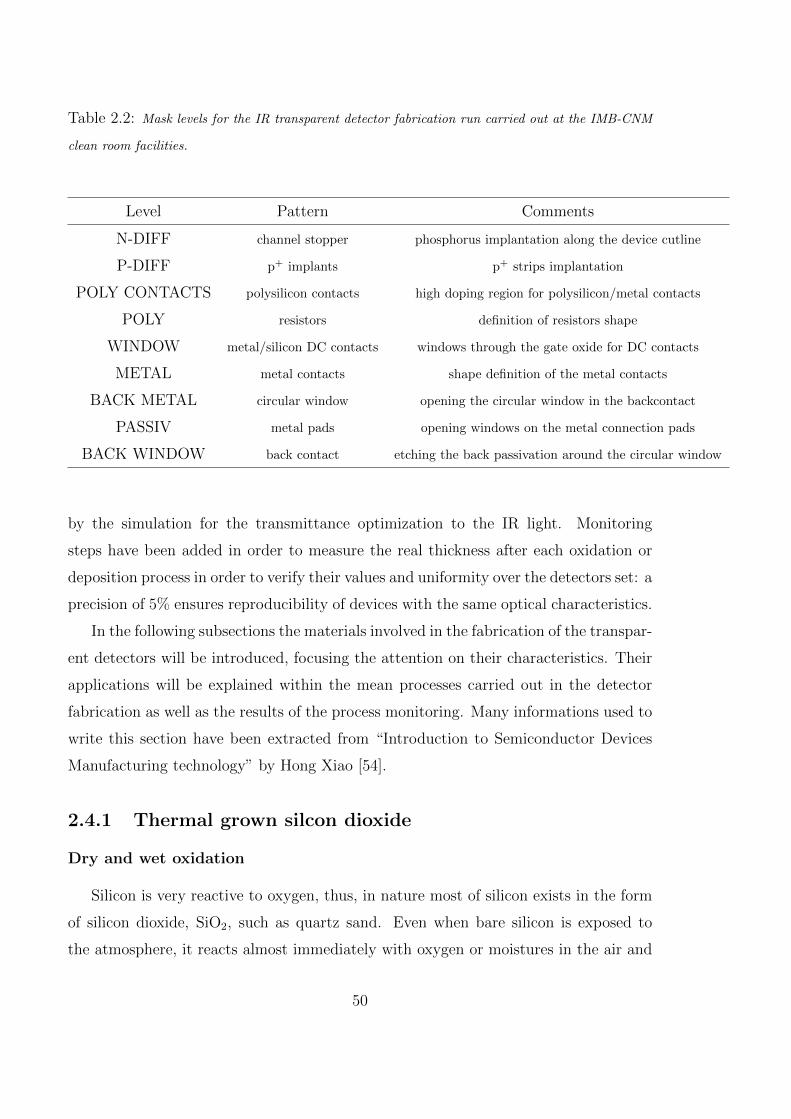
Table 2.2: Mask levels for the IR transparent detector fabrication run carried out at the IMB-CNM
clean room facilities.
Level Pattern Comments
N-DIFF channel stopper phosphorus implantation along the device cutline
P-DIFF p+ implants p+ strips implantation
POLY CONTACTS polysilicon contacts high doping region for polysilicon/metal contacts
POLY resistors definition of resistors shape
WINDOW metal/silicon DC contacts windows through the gate oxide for DC contacts
METAL metal contacts shape definition of the metal contacts
BACK METAL circular window opening the circular window in the backcontact
PASSIV metal pads opening windows on the metal connection pads
BACK WINDOW back contact etching the back passivation around the circular window
by the simulation for the transmittance optimization to the IR light. Monitoring
steps have been added in order to measure the real thickness after each oxidation or
deposition process in order to verify their values and uniformity over the detectors set: a
precision of 5% ensures reproducibility of devices with the same optical characteristics.
In the following subsections the materials involved in the fabrication of the transpar-
ent detectors will be introduced, focusing the attention on their characteristics. Their
applications will be explained within the mean processes carried out in the detector
fabrication as well as the results of the process monitoring. Many informations used to
write this section have been extracted from \Introduction to Semiconductor Devices
Manufacturing technology" by Hong Xiao [54].
2.4.1 Thermal grown silcon dioxide
Dry and wet oxidation
Silicon is very reactive to oxygen, thus, in nature most of silicon exists in the form
of silicon dioxide, SiO2, such as quartz sand. Even when bare silicon is exposed to
the atmosphere, it reacts almost immediately with oxygen or moistures in the air and
50
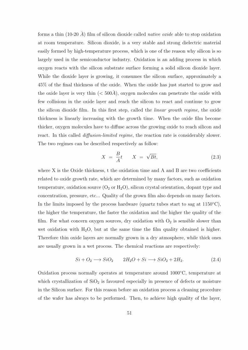
forms a thin (10-20 A) lm of silicon dioxide called native oxide able to stop oxidation
at room temperature. Silicon dioxide, is a very stable and strong dielectric material
easily formed by high-temperature process, which is one of the reason why silicon is so
largely used in the semiconductor industry. Oxidation is an adding process in which
oxygen reacts with the silicon substrate surface forming a solid silicon dioxide layer.
While the dioxide layer is growing, it consumes the silicon surface, approximately a
45% of the nal thickness of the oxide. When the oxide has just started to grow and
the oxide layer is very thin (< 500A), oxygen molecules can penetrate the oxide with
few collisions in the oxide layer and reach the silicon to react and continue to grow
the silicon dioxide lm. In this rst step, called the linear growth regime, the oxide
thickness is linearly increasing with the growth time. When the oxide lm become
thicker, oxygen molecules have to diuse across the growing oxide to reach silicon and
react. In this called diusion-limited regime, the reaction rate is considerably slower.
The two regimes can be described respectively as follow:
X =B
At X =
pBt; (2.3)
where X is the Oxide thickness, t the oxidation time and A and B are two coecients
related to oxide growth rate, which are determined by many factors, such as oxidation
temperature, oxidation source (O2 or H2O), silicon crystal orientation, dopant type and
concentration, pressure, etc... Quality of the grown lm also depends on many factors.
In the limits imposed by the process hardware (quartz tubes start to sag at 1150C),
the higher the temperature, the faster the oxidation and the higher the quality of the
lm. For what concern oxygen sources, dry oxidation with O2 is sensible slower than
wet oxidation with H2O, but at the same time the lm quality obtained is higher.
Therefore thin oxide layers are normally grown in a dry atmosphere, while thick ones
are usually grown in a wet process. The chemical reactions are respectively:
Si+O2 ! SiO2 2H2O + Si ! SiO2 + 2H2: (2.4)
Oxidation process normally operates at temperature around 1000C, temperature at
which crystallization of SiO2 is favoured especially in presence of defects or moisture
in the Silicon surface. For this reason before an oxidation process a cleaning procedure
of the wafer has always to be performed. Then, to achieve high quality of the layer,
51

special attention has to be paid to the resultant silicon-silicon dioxide interface, where
always dangling bonds are left because of the crystal structure mismatch, as shown
in gure 2.11. These dangling bonds induce so-called interface state charge, which is
positive charge that aect the performance of the device (section 1.2.4). Therefore, in
dry oxidation, proper concentration of HCl is commonly used for chlorine property of
integrating into silicon dioxide layer and binding with silicon at silicon-silicon dioxide
interface.
Figure 2.11: Dangling bonds at the silicon-silicon dioxide interface. Full circles represents oxygen
atoms while empty ones represents silicon atoms.
Using vaporized H2O instead of O2 as the oxygen source, steam oxide can be ob-
tained by means of a faster oxidation. The disadvantage is a less quality of the oxide.
For this reason after the initial temperature ramp-up and temperature stabilization
steps of the wet process, O2 ows are used to help growing a thin layer (few hundreds
A) of better quality oxide on the wafer surface as a barrier layer for the less-high quality
steam oxide and to reduce defects at the silicon-silicon dioxide interface. In the same
way before the nal temperature ramp-down a dry oxidation is used to dene a better
nal silicon -silicon oxide interface.
Oxidation is not selective on the wafer surface. In each process SiO2 grows in both
sides of the substrate.
Silicon dioxide grown by both dry and wet oxidation show the same optical char-
acteristic, with refraction index like in gure 2.3
52
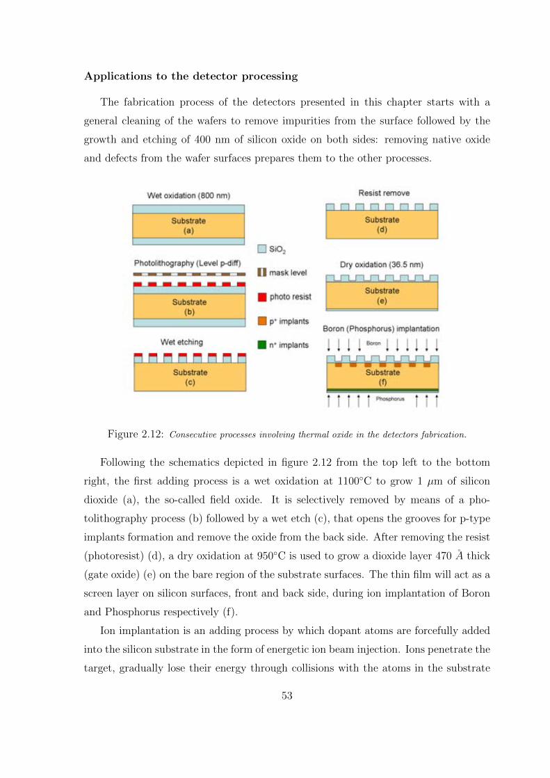
Applications to the detector processing
The fabrication process of the detectors presented in this chapter starts with a
general cleaning of the wafers to remove impurities from the surface followed by the
growth and etching of 400 nm of silicon oxide on both sides: removing native oxide
and defects from the wafer surfaces prepares them to the other processes.
Figure 2.12: Consecutive processes involving thermal oxide in the detectors fabrication.
Following the schematics depicted in gure 2.12 from the top left to the bottom
right, the rst adding process is a wet oxidation at 1100C to grow 1 m of silicon
dioxide (a), the so-called eld oxide. It is selectively removed by means of a pho-
tolithography process (b) followed by a wet etch (c), that opens the grooves for p-type
implants formation and remove the oxide from the back side. After removing the resist
(photoresist) (d), a dry oxidation at 950C is used to grow a dioxide layer 470 A thick
(gate oxide) (e) on the bare region of the substrate surfaces. The thin lm will act as a
screen layer on silicon surfaces, front and back side, during ion implantation of Boron
and Phosphorus respectively (f).
Ion implantation is an adding process by which dopant atoms are forcefully added
into the silicon substrate in the form of energetic ion beam injection. Ions penetrate the
target, gradually lose their energy through collisions with the atoms in the substrate
53

and eventually rest inside the substrate. The distance reached from the substrate
surface, the so-called projected range, depends on the energy of the ions, and generally
for a monoenergetic beam has a Gaussian distribution, because of dierent path each
ion follows. Due to the single-crystal structure of the silicon wafer, channeling eect
can interest ions impinging vertically on the silicon surface, letting them penetrate
deeply into the substrate, originating tails in the dopant distribution, i.e. anomalies
in the semiconductor junction. Implantation through a thin layer of screen silicon
dioxide (in this case the same 470 A thick gate oxide) can reduce this eect. Crossing
an amorphous material, implanted ions collide with and scatter silicon and oxygen
atoms reaching the silicon crystal with a dierent pitch angle. Moreover, channeling
can be reduced using a non zero tilt angle (7 in our process) during implantation.
A thicker layer of silicon dioxide, 1 m thick eld oxide, acts as a barrier for ions,
totally screening substrate regions under its pattern, so the process does not need any
other protection on the surface. A nal high temperature annealing helps recovering
silicon lattice damages close to the surface and diuse and activate dopants into the
substrate. Table 2.3 summarizes the parameters of ion implantation processes included
in the detectors fabrication.
Table 2.3: Parameters of ion implantation.
Dopant Dose [at/cm2] Energy [keV] Final conc. [at/cm2] Junction depth [m]
Boron 1.51014 100 1020 1
Phosphorus 11013 50 1019 1
Process monitoring
Thickness and uniformity of eld and gate oxide on the front side of the wafers
have been measured with the use of a NANOSPEC 6100 spectroscopic re ectometer
able to measure the thicknesses of up to three dierent layers of transparent materials.
Measurements took place in the same clean room facilities where the fabrication pro-
cesses were carried out, preserving wafers from external contamination. For each wafer
measurements have been performed in 5 dierent points distributed within its surface.
54
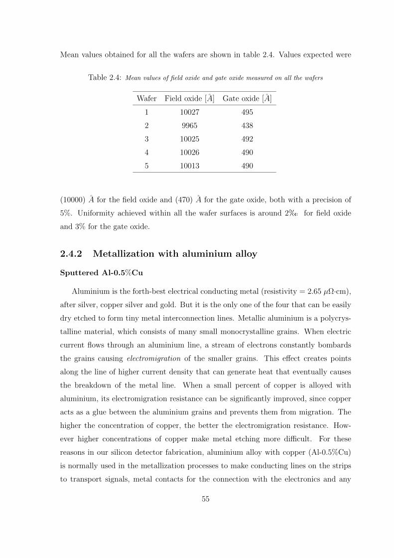
Mean values obtained for all the wafers are shown in table 2.4. Values expected were
Table 2.4: Mean values of eld oxide and gate oxide measured on all the wafers
Wafer Field oxide [A] Gate oxide [A]
1 10027 495
2 9965 438
3 10025 492
4 10026 490
5 10013 490
(10000) A for the eld oxide and (470) A for the gate oxide, both with a precision of
5%. Uniformity achieved within all the wafer surfaces is around 2 for eld oxide
and 3% for the gate oxide.
2.4.2 Metallization with aluminium alloy
Sputtered Al-0.5%Cu
Aluminium is the forth-best electrical conducting metal (resistivity = 2.65 cm),
after silver, copper silver and gold. But it is the only one of the four that can be easily
dry etched to form tiny metal interconnection lines. Metallic aluminium is a polycrys-
talline material, which consists of many small monocrystalline grains. When electric
current ows through an aluminium line, a stream of electrons constantly bombards
the grains causing electromigration of the smaller grains. This eect creates points
along the line of higher current density that can generate heat that eventually causes
the breakdown of the metal line. When a small percent of copper is alloyed with
aluminium, its electromigration resistance can be signicantly improved, since copper
acts as a glue between the aluminium grains and prevents them from migration. The
higher the concentration of copper, the better the electromigration resistance. How-
ever higher concentrations of copper make metal etching more dicult. For these
reasons in our silicon detector fabrication, aluminium alloy with copper (Al-0.5%Cu)
is normally used in the metallization processes to make conducting lines on the strips
to transport signals, metal contacts for the connection with the electronics and any
55
other conductive layer in the devices. Sputtering deposition is the physical vapour
deposition (PVD) process used for metallization. It consists in bombarding a target
of the aluminium alloy with highly accelerated ions from an argon plasma. Repeated
collisions generate atoms dislodging from the target surface. These free atoms travel
inside the vacuum in the form of metal vapour. When they reach the surface of the
wafer, they move on it clustering around nucleation sites in single-crystal structure,
generating the grains. When the grains grow and meet with other grains, they form
a continuous polycrystalline metal thin lm. The border between grains can scatter
electron ows and cause higher resistivity. So the bigger the grains, the better the
conductivity. Dimension of the grains also in uences re ectivity of the metal lm: the
smaller the grains, the higher the re ectivity. High re ectivity of the metal layer is
normally undesirable because it aects the precision of the pattern denition through
the photolithography process. In this particular case lower re ectivity translate also
into higher transmittance of the laser light for the alignment system. The grain size
is mainly determined by surface mobility of the atoms during the sputtering process,
which is related to many factors, such as wafer temperature. Normally higher tem-
perature results in larger-sized grains. Since a metal lm with large grain size is hard
to etch with smooth sidewalls, it is preferred to deposit the metal with smaller grain
size at lower temperatures and anneal the lm at higher temperature after the metal
etch and photoresist strip. Melting point of aluminium is relatively low, 660C, so
after metallization processes on the wafer, any other thermal process exceeding 450C
is forbidden.
Metallization process steps
The rst metal layer is deposited just after the processes dedicated to the bias
resistors formation, that will be explained in section 2.4.5. The main processes are
depicted in gures 2.13 and 2.14. Starting from gure 2.13, the aluminium alloy
with copper is sputtered on the front side to form a layer 950 nm thick (a), on which
a photolytography (b) and a wet etching processes (c) are then used to dene the
strips on the implants. Figures refers to the particular case of a detector (S5) with
intermediate strips and implants (metal) width equal to 15 (5) m. Meanwhile, the
back surface of the wafer is protected by a thin (470 A) lm of silicon dioxide covered
56
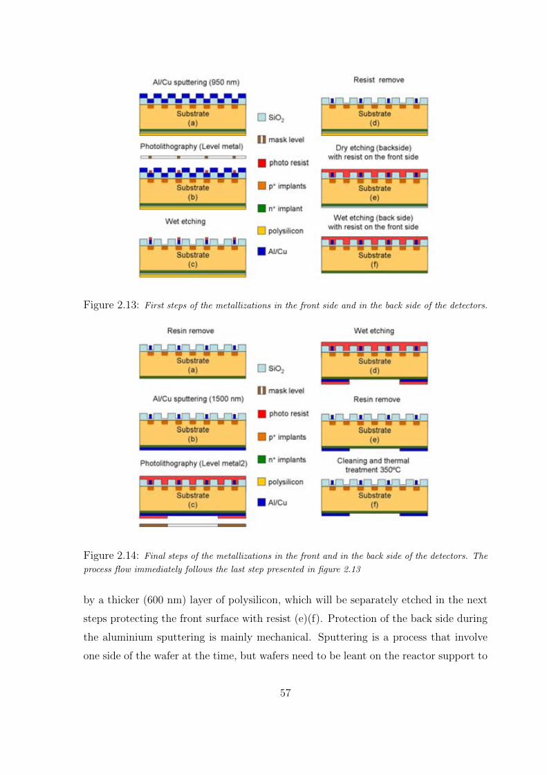
Figure 2.13: First steps of the metallizations in the front side and in the back side of the detectors.
Figure 2.14: Final steps of the metallizations in the front and in the back side of the detectors. The
process flow immediately follows the last step presented in figure 2.13
by a thicker (600 nm) layer of polysilicon, which will be separately etched in the next
steps protecting the front surface with resist (e)(f). Protection of the back side during
the aluminium sputtering is mainly mechanical. Sputtering is a process that involve
one side of the wafer at the time, but wafers need to be leant on the reactor support to
57
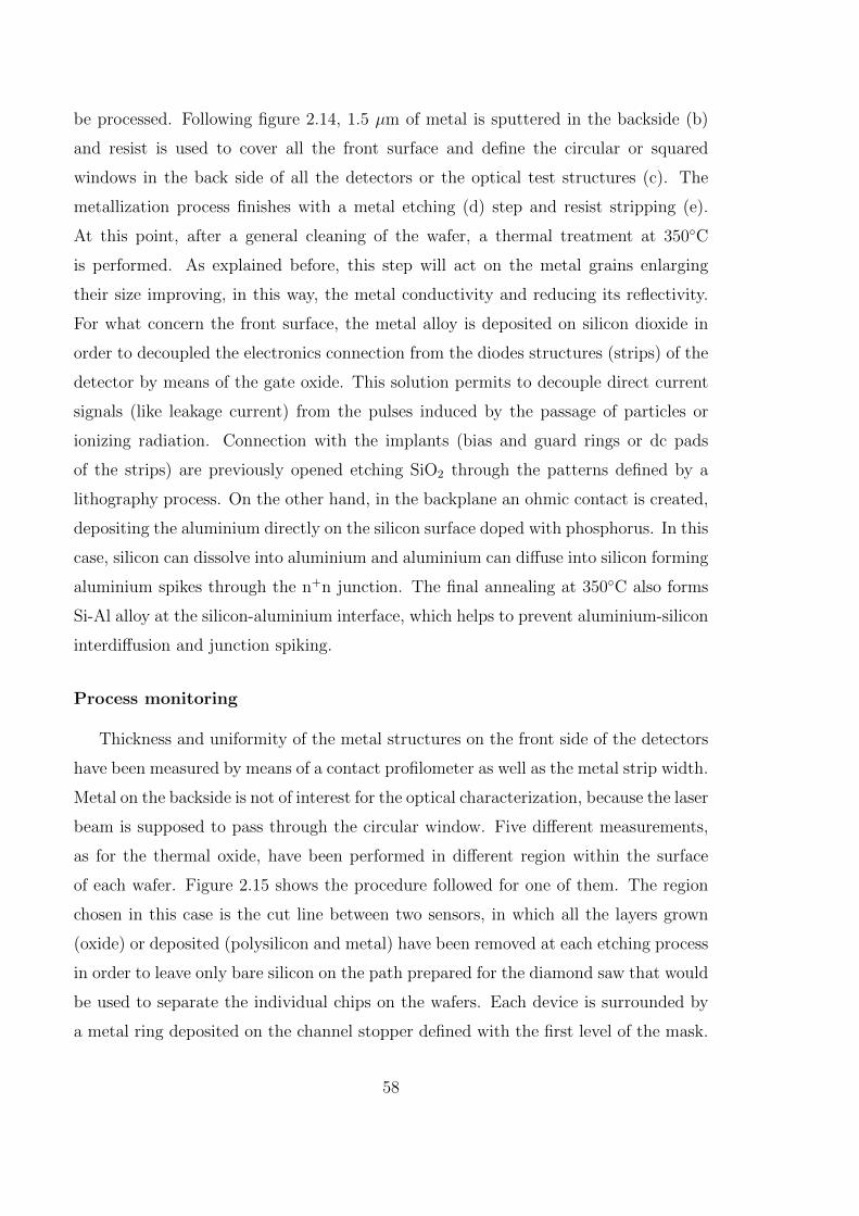
be processed. Following gure 2.14, 1.5 m of metal is sputtered in the backside (b)
and resist is used to cover all the front surface and dene the circular or squared
windows in the back side of all the detectors or the optical test structures (c). The
metallization process nishes with a metal etching (d) step and resist stripping (e).
At this point, after a general cleaning of the wafer, a thermal treatment at 350C
is performed. As explained before, this step will act on the metal grains enlarging
their size improving, in this way, the metal conductivity and reducing its re ectivity.
For what concern the front surface, the metal alloy is deposited on silicon dioxide in
order to decoupled the electronics connection from the diodes structures (strips) of the
detector by means of the gate oxide. This solution permits to decouple direct current
signals (like leakage current) from the pulses induced by the passage of particles or
ionizing radiation. Connection with the implants (bias and guard rings or dc pads
of the strips) are previously opened etching SiO2 through the patterns dened by a
lithography process. On the other hand, in the backplane an ohmic contact is created,
depositing the aluminium directly on the silicon surface doped with phosphorus. In this
case, silicon can dissolve into aluminium and aluminium can diuse into silicon forming
aluminium spikes through the n+n junction. The nal annealing at 350C also forms
Si-Al alloy at the silicon-aluminium interface, which helps to prevent aluminium-silicon
interdiusion and junction spiking.
Process monitoring
Thickness and uniformity of the metal structures on the front side of the detectors
have been measured by means of a contact prolometer as well as the metal strip width.
Metal on the backside is not of interest for the optical characterization, because the laser
beam is supposed to pass through the circular window. Five dierent measurements,
as for the thermal oxide, have been performed in dierent region within the surface
of each wafer. Figure 2.15 shows the procedure followed for one of them. The region
chosen in this case is the cut line between two sensors, in which all the layers grown
(oxide) or deposited (polysilicon and metal) have been removed at each etching process
in order to leave only bare silicon on the path prepared for the diamond saw that would
be used to separate the individual chips on the wafers. Each device is surrounded by
a metal ring deposited on the channel stopper dened with the rst level of the mask.
58
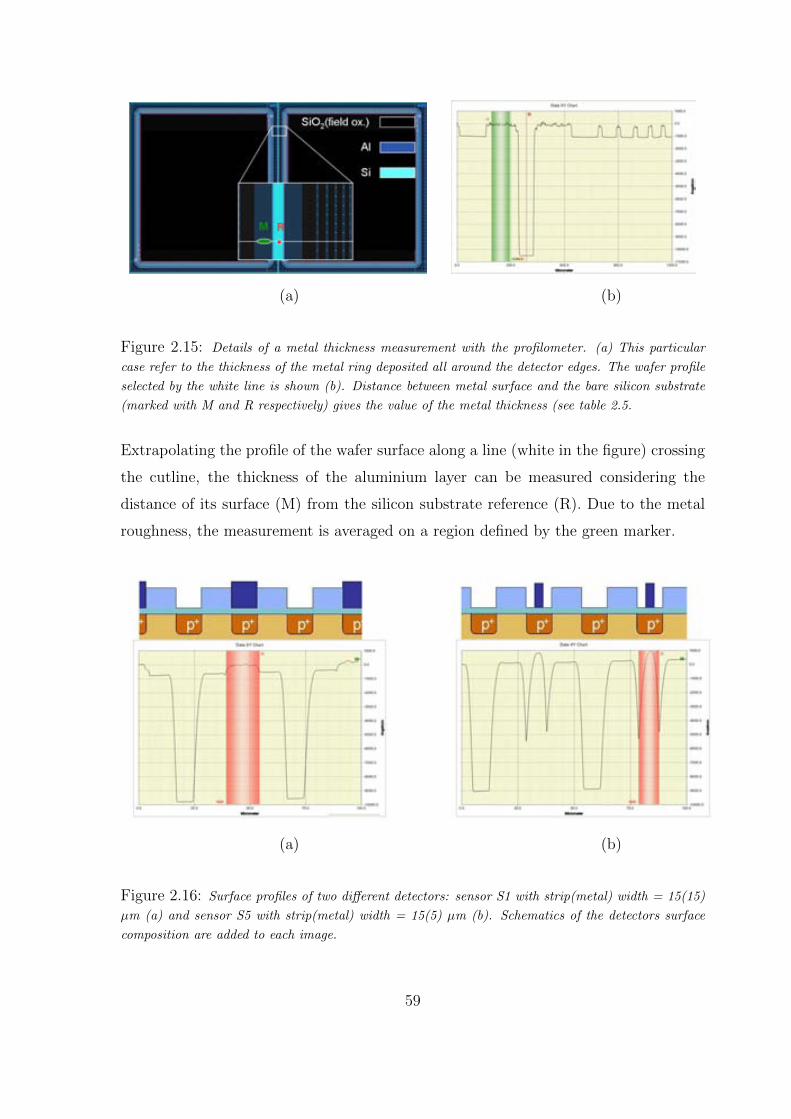
(a) (b)
Figure 2.15: Details of a metal thickness measurement with the prolometer. (a) This particular
case refer to the thickness of the metal ring deposited all around the detector edges. The wafer prole
selected by the white line is shown (b). Distance between metal surface and the bare silicon substrate
(marked with M and R respectively) gives the value of the metal thickness (see table 2.5.
Extrapolating the prole of the wafer surface along a line (white in the gure) crossing
the cutline, the thickness of the aluminium layer can be measured considering the
distance of its surface (M) from the silicon substrate reference (R). Due to the metal
roughness, the measurement is averaged on a region dened by the green marker.
(a) (b)
Figure 2.16: Surface proles of two dierent detectors: sensor S1 with strip(metal) width = 15(15)
m (a) and sensor S5 with strip(metal) width = 15(5) m (b). Schematics of the detectors surface
composition are added to each image.
59
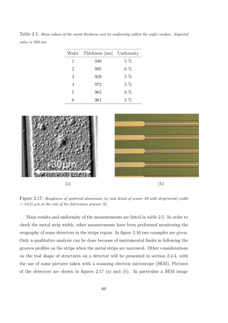
Table 2.5: Mean values of the metal thickness and its uniformity within the wafer surface. Expected
value is 950 nm.
Wafer Thickness [nm] Uniformity
1 940 5 %
2 995 6 %
3 929 5 %
4 972 5 %
5 965 6 %
6 961 5 %
(a) (b)
Figure 2.17: Roughness of sputtered aluminium (a) and detail of sensor S9 with strip(metal) width
= 15(3) µ m at the end of the fabrication process (b).
Main results and uniformity of the measurements are listed in table 2.5. In order to
check the metal strip width, other measurements have been performed monitoring the
orography of some detectors in the strips region. In figure 2.16 two examples are given.
Only a qualitative analysis can be done because of instrumental limits in following the
grooves profiles on the strips when the metal strips are narrowed. Other considerations
on the real shape of structures on a detector will be presented in section 2.4.4, with
the use of some pictures taken with a scanning electron microscope (SEM). Pictures
of the detectors are shown in figures 2.17 (a) and (b). In particular a SEM image
60
of a 30 m wide strip of Aluminium and its grains composition are shown. Value of
40 nm roughness has been measured and used in the detector model to better predict
re ectivity of aluminium in the optical simulation: re ection, no absorption, result to
be the main interaction of aluminium with IR light. The second picture, taken with an
optical microscope, refers to a detail of sensor S9 in the region where the metal lines
meet the electric pads on the strips.
2.4.3 Passivation: an anti-re ection coating
PECVD of SiO2 and Si3N4
After the last metal layer denition, a passivation layer is normally deposited on
the wafer to protect the chips from impurities, moisture or scratches. A good barrier
layer deposited at low temperature (< 450C) with high dielectric strength and high
mechanical strength is demanded for a reliable passivation. Silicon nitride satisfy all
of these requirements and is commonly used as the last passivation layer, deposited
on a silicon oxide pad layer, as a buer against strong tensile stress of nitride. Both
Table 2.6: Properties of oxide and nitride.
Oxide (SiO2) Nitride (Si3N4)
High dielectric strength, > 1 107 V/cm High dielectric strength, > 1 107 V/cm
Lower dielectric constant, k = 3.9 Higher dielectric constant, k = 7.0
Not a good barrier for moisture and mobile ions Good barrier for moisture and mobile ions
Refraction index ( = 633 ns), n = 1.46 Refraction index ( = 633 ns), n = 2.01
silicon oxide and silicon nitride are good electrical insulators with very high dielec-
tric strength (breakdown voltage). Referring to table 2.6, where stoichiometric values
are listed, silicon oxide has a lower dielectric constant than silicon nitride. Therefore,
using oxide (thermal or deposited) in interconnection applications causes a smaller
parasitic capacitance between the metal lines. On the other hand, silicon nitride pro-
vides more moisture and mobile-ion barrier than oxide, that leads denitely to the
choice of silicon nitride as the last layer deposited on a chip. From an optical point of
view, things are dierent. As explained in section 2.2, when the light impinges on the
61
interface between two homogeneous media with dierent refraction index, its energy
is split between re ected and transmitted waves. The higher the dierence between
the refraction indices, the higher the portion of energy re ected. Considering that the
refractive index of silicon is 3.88 at = 633 nm, then the layers order Si-Si3N4-SiO2
would improve transmittance of light if used instead of the conventional Si-SiO2-Si3N4.
Nevertheless, remembering that the aim of this work is improving light transmittance
without aecting detector operation and considering the above issues, the last sequence,
Si-SiO2-Si3N4, is the one used for these devices too. In section 2.6 we will see how,
even in this conguration, a proper choice of the thickness of the last layers of silicon
nitride (covering both the front and back surface), can improve transmittance of the
laser light.
A silane-based Plasma Enhanced Chemical Vapor Deposition (PECVD) chamber
can deposit both oxide and nitride with one process sequence, respecting the temper-
ature limits imposed by the aluminium metallizations on the wafer.
CVD is a process in which gaseous chemical precursor(s) has (have) a chemical
reaction on the wafer surface depositing a layer of solid by-product. This happens in
a sequential process including several steps. The precursors introduced in the reactor
diuse across the boundary layer and impinge on the surface where they are absorbed
by the substrate and start migrate on the surface till a chemical reaction takes place
creating a solid material. The rst few molecules of the solid material form nuclei on the
surface, and further chemical reactions cause the nuclei to grow into islands that grow,
merge and nally form a continuous thin lm on the wafer surface. Since the steps in a
CVD process are sequential, the one that occurs at the slowest rate will determine the
deposition rate. Gas-phase processes dictate the rate at which gases impinge on the
surface and are only weakly in uenced by the deposition temperature. On the other
hand, the surface reaction rate dependence on temperature can be expressed in this
way:
R = A exp(Ea=kT ); (2.5)
where A is the frequency factor, Ea is the activation energy, k is the Boltzmann constant
and T the absolute temperature. High deposition rate normally translates into high
homogeneity of the layer deposited.
In PECVD, a radio frequency (RF) glow discharge can transfer energy into the
62
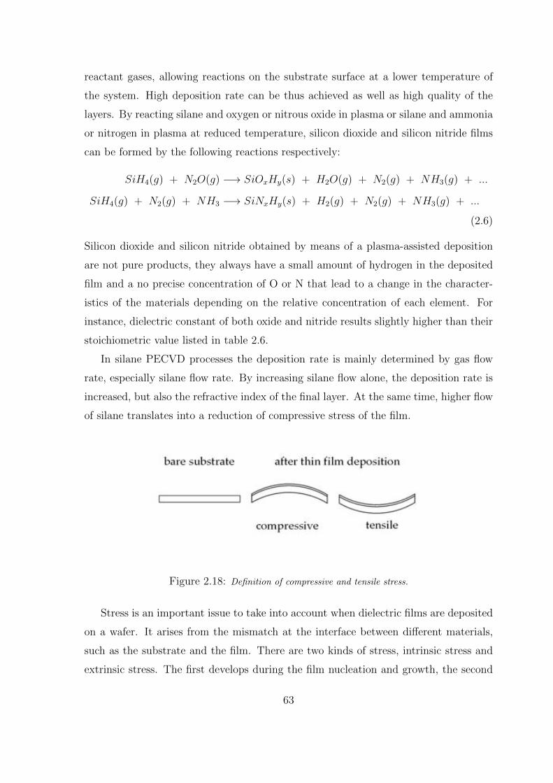
reactant gases, allowing reactions on the substrate surface at a lower temperature of
the system. High deposition rate can be thus achieved as well as high quality of the
layers. By reacting silane and oxygen or nitrous oxide in plasma or silane and ammonia
or nitrogen in plasma at reduced temperature, silicon dioxide and silicon nitride lms
can be formed by the following reactions respectively:
SiH4(g) + N2O(g) ! SiOxHy(s) + H2O(g) + N2(g) + NH3(g) + :::
SiH4(g) + N2(g) + NH3 ! SiNxHy(s) + H2(g) + N2(g) + NH3(g) + :::
(2.6)
Silicon dioxide and silicon nitride obtained by means of a plasma-assisted deposition
are not pure products, they always have a small amount of hydrogen in the deposited
lm and a no precise concentration of O or N that lead to a change in the character-
istics of the materials depending on the relative concentration of each element. For
instance, dielectric constant of both oxide and nitride results slightly higher than their
stoichiometric value listed in table 2.6.
In silane PECVD processes the deposition rate is mainly determined by gas ow
rate, especially silane ow rate. By increasing silane ow alone, the deposition rate is
increased, but also the refractive index of the nal layer. At the same time, higher ow
of silane translates into a reduction of compressive stress of the lm.
Figure 2.18: Denition of compressive and tensile stress.
Stress is an important issue to take into account when dielectric lms are deposited
on a wafer. It arises from the mismatch at the interface between dierent materials,
such as the substrate and the lm. There are two kinds of stress, intrinsic stress and
extrinsic stress. The rst develops during the lm nucleation and growth, the second
63
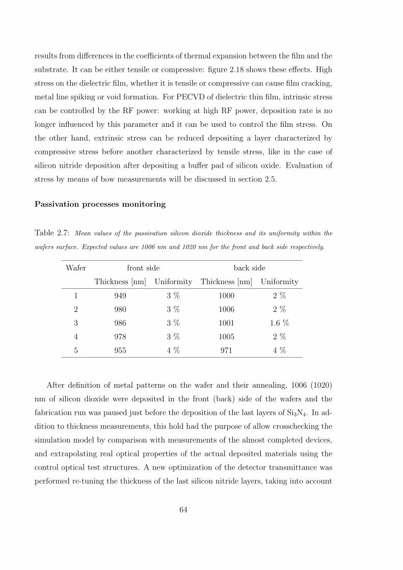
results from dierences in the coecients of thermal expansion between the lm and the
substrate. It can be either tensile or compressive: gure 2.18 shows these eects. High
stress on the dielectric lm, whether it is tensile or compressive can cause lm cracking,
metal line spiking or void formation. For PECVD of dielectric thin lm, intrinsic stress
can be controlled by the RF power: working at high RF power, deposition rate is no
longer in uenced by this parameter and it can be used to control the lm stress. On
the other hand, extrinsic stress can be reduced depositing a layer characterized by
compressive stress before another characterized by tensile stress, like in the case of
silicon nitride deposition after depositing a buer pad of silicon oxide. Evaluation of
stress by means of bow measurements will be discussed in section 2.5.
Passivation processes monitoring
Table 2.7: Mean values of the passivation silicon dioxide thickness and its uniformity within the
wafers surface. Expected values are 1006 nm and 1020 nm for the front and back side respectively.
Wafer front side back side
Thickness [nm] Uniformity Thickness [nm] Uniformity
1 949 3 % 1000 2 %
2 980 3 % 1006 2 %
3 986 3 % 1001 1.6 %
4 978 3 % 1005 2 %
5 955 4 % 971 4 %
After denition of metal patterns on the wafer and their annealing, 1006 (1020)
nm of silicon dioxide were deposited in the front (back) side of the wafers and the
fabrication run was paused just before the deposition of the last layers of Si3N4. In ad-
dition to thickness measurements, this hold had the purpose of allow crosschecking the
simulation model by comparison with measurements of the almost completed devices,
and extrapolating real optical properties of the actual deposited materials using the
control optical test structures. A new optimization of the detector transmittance was
performed re-tuning the thickness of the last silicon nitride layers, taking into account
64
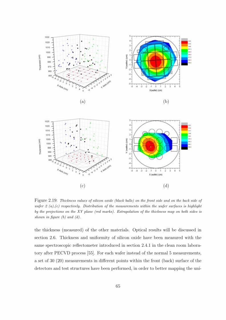
(a) (b)
(c) (d)
Figure 2.19: Thickness values of silicon oxide (black balls) on the front side and on the back side of
wafer 2 (a),(c) respectively. Distribution of the measurements within the wafer surfaces is highlight
by the projections on the XY plane (red marks). Extrapolation of the thickness map on both sides is
shown in gure (b) and (d).
the thickness (measured) of the other materials. Optical results will be discussed in
section 2.6. Thickness and uniformity of silicon oxide have been measured with the
same spectroscopic re ectometer introduced in section 2.4.1 in the clean room labora-
tory after PECVD process [55]. For each wafer instead of the normal 5 measurements,
a set of 30 (20) measurements in dierent points within the front (back) surface of the
detectors and test structures have been performed, in order to better mapping the uni-
65
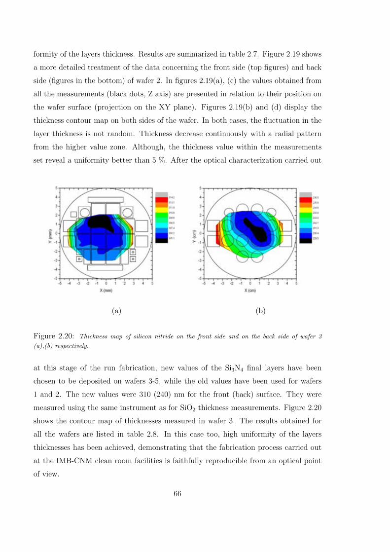
formity of the layers thickness. Results are summarized in table 2.7. Figure 2.19 shows
a more detailed treatment of the data concerning the front side (top gures) and back
side (gures in the bottom) of wafer 2. In gures 2.19(a), (c) the values obtained from
all the measurements (black dots, Z axis) are presented in relation to their position on
the wafer surface (projection on the XY plane). Figures 2.19(b) and (d) display the
thickness contour map on both sides of the wafer. In both cases, the uctuation in the
layer thickness is not random. Thickness decrease continuously with a radial pattern
from the higher value zone. Although, the thickness value within the measurements
set reveal a uniformity better than 5 %. After the optical characterization carried out
(a) (b)
Figure 2.20: Thickness map of silicon nitride on the front side and on the back side of wafer 3
(a),(b) respectively.
at this stage of the run fabrication, new values of the Si3N4 nal layers have been
chosen to be deposited on wafers 3-5, while the old values have been used for wafers
1 and 2. The new values were 310 (240) nm for the front (back) surface. They were
measured using the same instrument as for SiO2 thickness measurements. Figure 2.20
shows the contour map of thicknesses measured in wafer 3. The results obtained for
all the wafers are listed in table 2.8. In this case too, high uniformity of the layers
thicknesses has been achieved, demonstrating that the fabrication process carried out
at the IMB-CNM clean room facilities is faithfully reproducible from an optical point
of view.
66

Table 2.8: Mean values of the passivation silicon nitride thickness and its uniformity within the
wafer surfaces. Expected values are (104650) nm and (100550) nm for wafer 1 and 2 in the front
and back side respectively, (31016) nm and (24012) nm for wafer 3,4 and 5 in the front and back
side respectively.
Wafer front side back side
Thickness [nm] Uniformity Thickness [nm] Uniformity
1 1075 2 % 1013 1.5 %
2 1052 2 % 1025 1.9 %
3 308 1.5 % 232 1.5 %
4 304 2 % 234 1.6 %
5 306 2 % 234 1.5 %
The last processes performed are photolitography steps to dene the openings for
the bonding pads in the front side, and to open the ohmic contact around the passivated
window in the back side, obtaining the nal cross section shown in gure 2.21.
Figure 2.21: Schematic cross section of a sensor in the contacts pad region.
2.4.4 Etch and deposition prole
The previous sections described the most important materials of optical interest
and the related processes used to fabricate the transparent detectors with emphasis
on growth or deposition of the dierent material layers. Photolithography has been
introduced as the patterning process used to transfer the design pattern from the mask
to the wafer, followed by either etch or implantation through the pattern dened on
67
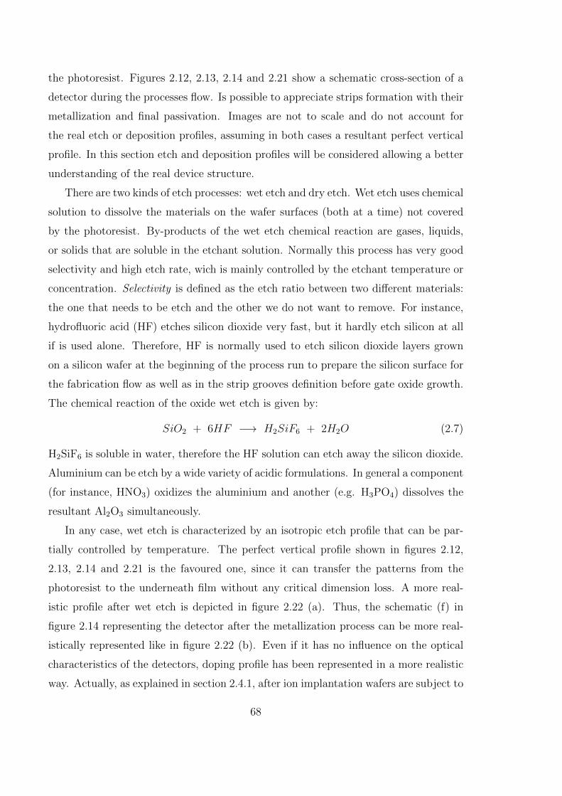
the photoresist. Figures 2.12, 2.13, 2.14 and 2.21 show a schematic cross-section of a
detector during the processes ow. Is possible to appreciate strips formation with their
metallization and nal passivation. Images are not to scale and do not account for
the real etch or deposition proles, assuming in both cases a resultant perfect vertical
prole. In this section etch and deposition proles will be considered allowing a better
understanding of the real device structure.
There are two kinds of etch processes: wet etch and dry etch. Wet etch uses chemical
solution to dissolve the materials on the wafer surfaces (both at a time) not covered
by the photoresist. By-products of the wet etch chemical reaction are gases, liquids,
or solids that are soluble in the etchant solution. Normally this process has very good
selectivity and high etch rate, wich is mainly controlled by the etchant temperature or
concentration. Selectivity is dened as the etch ratio between two dierent materials:
the one that needs to be etch and the other we do not want to remove. For instance,
hydro uoric acid (HF) etches silicon dioxide very fast, but it hardly etch silicon at all
if is used alone. Therefore, HF is normally used to etch silicon dioxide layers grown
on a silicon wafer at the beginning of the process run to prepare the silicon surface for
the fabrication ow as well as in the strip grooves denition before gate oxide growth.
The chemical reaction of the oxide wet etch is given by:
SiO2 + 6HF ! H2SiF6 + 2H2O (2.7)
H2SiF6 is soluble in water, therefore the HF solution can etch away the silicon dioxide.
Aluminium can be etch by a wide variety of acidic formulations. In general a component
(for instance, HNO3) oxidizes the aluminium and another (e.g. H3PO4) dissolves the
resultant Al2O3 simultaneously.
In any case, wet etch is characterized by an isotropic etch prole that can be par-
tially controlled by temperature. The perfect vertical prole shown in gures 2.12,
2.13, 2.14 and 2.21 is the favoured one, since it can transfer the patterns from the
photoresist to the underneath lm without any critical dimension loss. A more real-
istic prole after wet etch is depicted in gure 2.22 (a). Thus, the schematic (f) in
gure 2.14 representing the detector after the metallization process can be more real-
istically represented like in gure 2.22 (b). Even if it has no in uence on the optical
characteristics of the detectors, doping prole has been represented in a more realistic
way. Actually, as explained in section 2.4.1, after ion implantation wafers are subject to
68
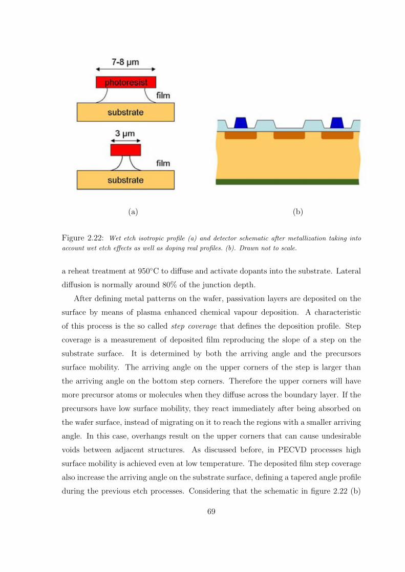
(a) (b)
Figure 2.22: Wet etch isotropic prole (a) and detector schematic after metallization taking into
account wet etch eects as well as doping real proles. (b). Drawn not to scale.
a reheat treatment at 950C to diuse and activate dopants into the substrate. Lateral
diusion is normally around 80% of the junction depth.
After dening metal patterns on the wafer, passivation layers are deposited on the
surface by means of plasma enhanced chemical vapour deposition. A characteristic
of this process is the so called step coverage that denes the deposition prole. Step
coverage is a measurement of deposited lm reproducing the slope of a step on the
substrate surface. It is determined by both the arriving angle and the precursors
surface mobility. The arriving angle on the upper corners of the step is larger than
the arriving angle on the bottom step corners. Therefore the upper corners will have
more precursor atoms or molecules when they diuse across the boundary layer. If the
precursors have low surface mobility, they react immediately after being absorbed on
the wafer surface, instead of migrating on it to reach the regions with a smaller arriving
angle. In this case, overhangs result on the upper corners that can cause undesirable
voids between adjacent structures. As discussed before, in PECVD processes high
surface mobility is achieved even at low temperature. The deposited lm step coverage
also increase the arriving angle on the substrate surface, dening a tapered angle prole
during the previous etch processes. Considering that the schematic in gure 2.22 (b)
69
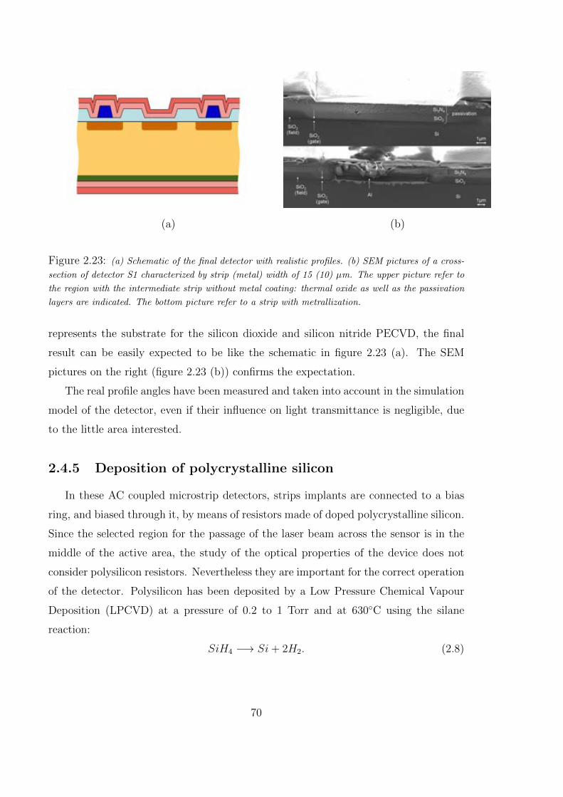
(a) (b)
Figure 2.23: (a) Schematic of the nal detector with realistic proles. (b) SEM pictures of a cross-
section of detector S1 characterized by strip (metal) width of 15 (10) m. The upper picture refer to
the region with the intermediate strip without metal coating: thermal oxide as well as the passivation
layers are indicated. The bottom picture refer to a strip with metrallization.
represents the substrate for the silicon dioxide and silicon nitride PECVD, the nal
result can be easily expected to be like the schematic in gure 2.23 (a). The SEM
pictures on the right (gure 2.23 (b)) conrms the expectation.
The real prole angles have been measured and taken into account in the simulation
model of the detector, even if their in uence on light transmittance is negligible, due
to the little area interested.
2.4.5 Deposition of polycrystalline silicon
In these AC coupled microstrip detectors, strips implants are connected to a bias
ring, and biased through it, by means of resistors made of doped polycrystalline silicon.
Since the selected region for the passage of the laser beam across the sensor is in the
middle of the active area, the study of the optical properties of the device does not
consider polysilicon resistors. Nevertheless they are important for the correct operation
of the detector. Polysilicon has been deposited by a Low Pressure Chemical Vapour
Deposition (LPCVD) at a pressure of 0.2 to 1 Torr and at 630C using the silane
reaction:
SiH4 ! Si+ 2H2: (2.8)
70
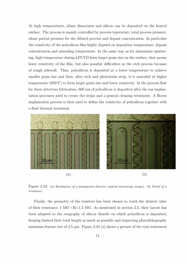
At high temperatures, silane dissociates and silicon can be deposited on the heated
surface. The process is mainly controlled by process teperature, total process pressure,
silane partial pressure for the diluted process and dopant concentration. In particular
the resistivity of the polysilicon lm highly depend on deposition temperature, dopant
concentration and annealing temperature. In the same way as for aluminium sputter-
ing, high temperature during LPCVD form larger grain size on the surface, that means
lower resistivity of the lm, but also possible diculties in the etch process because
of rough sidewall. Thus, polysilicon is deposited at a lower temperature to achieve
smaller grain size and then, after etch and photoresist strip, it is annealed at higher
temperature (950C) to form larger grain size and lower resistivity. In the process ow
for these detectors fabrication, 600 nm of polysilicon is deposited after the ion implan-
tation processes used to create the strips and a general cleaning treatment. A Boron
implantation process is then used to dene the resistivity of polysilicon together with
a nal thermal treatment.
(a) (b)
Figure 2.24: (a) Resistances of a transparent detector (optical microscope image). (b) Detail of a
resistance.
Finally, the geometry of the resistors has been chosen to reach the desired value
of their resistance, 1 M <R<1.5 M. As mentioned in section 2.3, their layout has
been adapted to the orography of silicon dioxide on which polysilicon is deposited,
keeping limited their total length as much as possible and respecting photolithography
minimum feature size of 2.5 m. Figure 2.24 (a) shows a picture of the real resistances
71

that can be compared to the mask design presented in gure 2.9 (b). Resistances
pattern has been transferred to the polysilicon layer by means of a dry etch process
using Cl2 as the main etchant. In plasma, Cl2 molecules dissociate to generate free
chlorine radicals, which are very reactive and can react with silicon and form gaseous
silicon tetrachloride. Chloride tends to combine with photoresist materials and deposit
a thin polymer layer on the side wall. This helps to achieve an anisotropic etch prole
obtaining the result shown by the SEM image, gure 2.24 (b).
O2 is used to improve selectivity over oxide. The electrical characterization of the
devices demonstrate that the value obtained for the bias resistance R=(1.350.13) M
is in perfect agreement with the expected value.
Pictures of the front and back sides of a wafer at the end of the fabrication process
are shown in gure 2.25.
(a) (b)
Figure 2.25: (a) Front side of a wafer at the end of the processes run. (b) Back side of the same
wafer at the end of the processes run.
2.5 Electrical characterization
The detectors have been electrically characterized in the IMB-CNM laboratories
with the use of a Cascade Microtech probe station with thermal chuck, two Keithley
2410 Source/Meters and an Agilent 4284A LCR Meter (see gure 2.26). For the C-V
72
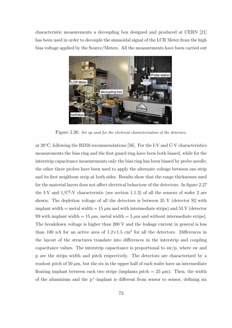
characteristic measurements a decoupling box designed and produced at CERN [21]
has been used in order to decouple the sinusoidal signal of the LCR Meter from the high
bias voltage applied by the Source/Meters. All the measurements have been carried out
Figure 2.26: Set up used for the electrical characterization of the detectors.
at 20C, following the RD50 recommendations [56]. For the I-V and C-V characteristics
measurements the bias ring and the rst guard ring have been both biased, while for the
interstrip capacitance measurements only the bias ring has been biased by probe needle;
the other three probes have been used to apply the alternate voltage between one strip
and its rst neighbour strip at both sides. Results show that the range thicknesses used
for the material layers does not aect electrical behaviour of the detectors. In gure 2.27
the I-V and 1/C2-V characteristic (see section 1.1.3) of all the sensors of wafer 2 are
shown. The depletion voltage of all the detectors is between 35 V (detector S2 with
implant width = metal width = 15 m and with intermediate strips) and 53 V (detector
S9 with implant width = 15 m, metal width = 5 m and without intermediate strips).
The breakdown voltage is higher than 200 V and the leakage current in general is less
than 100 nA for an active area of 1.21.5 cm2 for all the detectors. Dierences in
the layout of the structures translate into dierences in the interstrip and coupling
capacitance values. The interstrip capacitance is proportional to sw/p, where sw and
p are the strips width and pitch respectively. The detectors are characterized by a
readout pitch of 50 m, but the six in the upper half of each wafer have an intermediate
oating implant between each two strips (implants pitch = 25 m). Then, the width
of the aluminium and the p+-implant is dierent from sensor to sensor, dening six
73

(a) (b)
Figure 2.27: (a) 1/C2-V characteristic of the sensors of wafer 2. (b) I-V characteristic of the
sensors of wafer 2.
combinations. Figure 2.28 shows the results of the measurements and their dependence
on the layout parameters. Wider strips translate into higher interstrip and coupling
capacitance. The values related to the detectors with intermediate strips are lower than
the ones of the detectors without intermediate strips, but with the same strip/metal
design. For the detectors with strip width equal to 15 m the decrease is around 15%,
while it is less than 10% (more than 20%), for the sensors with strip width equal to
17.5 m (12.5 m).
For what concern the coupling capacitance, as expected it is smaller for the detector
with narrower electrodes: in this case the metal width has the higher in uence on the
measure. An error in the design of the contact pads of sensor S9 forbidded measuring
its coupling capacitance.
Finally, measurements of the wafer bow have been performed with a PROFORMA
300 by MTI, a manual, non-contact wafer metrology inspection system, in order to
monitor the eect of the passivation layers thickness on the total stress. It is measured
at the centre point of the wafer with a three point reference plane about the edge of
the wafer. Results are listed in table 2.9. Bare wafers before processing had a bow
varying in the range 10 m.
The sign minus denotes that the tensile stress of silicon nitride layer on the front
74
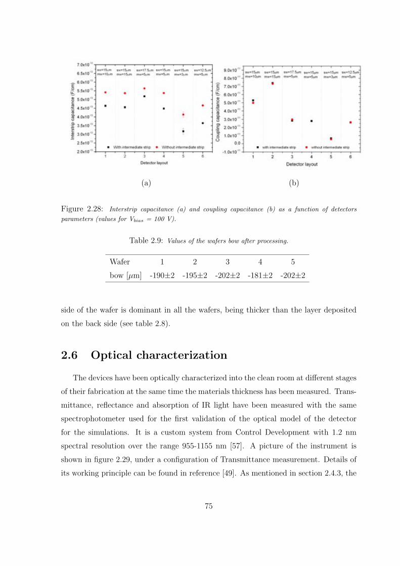
(a) (b)
Figure 2.28: Interstrip capacitance (a) and coupling capacitance (b) as a function of detectors
parameters (values for Vbias = 100 V).
Table 2.9: Values of the wafers bow after processing.
Wafer 1 2 3 4 5
bow [m] -1902 -1952 -2022 -1812 -2022
side of the wafer is dominant in all the wafers, being thicker than the layer deposited
on the back side (see table 2.8).
2.6 Optical characterization
The devices have been optically characterized into the clean room at dierent stages
of their fabrication at the same time the materials thickness has been measured. Trans-
mittance, re ectance and absorption of IR light have been measured with the same
spectrophotometer used for the rst validation of the optical model of the detector
for the simulations. It is a custom system from Control Development with 1.2 nm
spectral resolution over the range 955-1155 nm [57]. A picture of the instrument is
shown in gure 2.29, under a conguration of Transmittance measurement. Details of
its working principle can be found in reference [49]. As mentioned in section 2.4.3, the
75
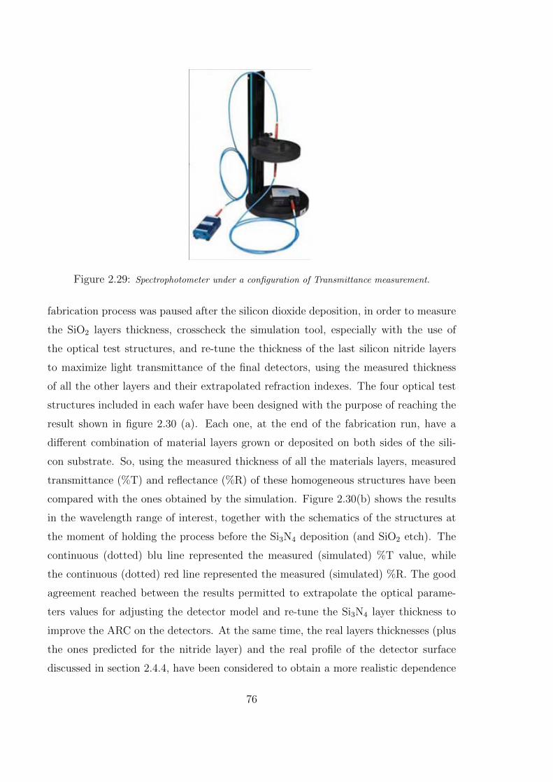
Figure 2.29: Spectrophotometer under a conguration of Transmittance measurement.
fabrication process was paused after the silicon dioxide deposition, in order to measure
the SiO2 layers thickness, crosscheck the simulation tool, especially with the use of
the optical test structures, and re-tune the thickness of the last silicon nitride layers
to maximize light transmittance of the nal detectors, using the measured thickness
of all the other layers and their extrapolated refraction indexes. The four optical test
structures included in each wafer have been designed with the purpose of reaching the
result shown in gure 2.30 (a). Each one, at the end of the fabrication run, have a
dierent combination of material layers grown or deposited on both sides of the sili-
con substrate. So, using the measured thickness of all the materials layers, measured
transmittance (%T) and re ectance (%R) of these homogeneous structures have been
compared with the ones obtained by the simulation. Figure 2.30(b) shows the results
in the wavelength range of interest, together with the schematics of the structures at
the moment of holding the process before the Si3N4 deposition (and SiO2 etch). The
continuous (dotted) blu line represented the measured (simulated) %T value, while
the continuous (dotted) red line represented the measured (simulated) %R. The good
agreement reached between the results permitted to extrapolate the optical parame-
ters values for adjusting the detector model and re-tune the Si3N4 layer thickness to
improve the ARC on the detectors. At the same time, the real layers thicknesses (plus
the ones predicted for the nitride layer) and the real prole of the detector surface
discussed in section 2.4.4, have been considered to obtain a more realistic dependence
76

(a) (b)
Figure 2.30: Optical test structures at the end of the fabrication process (a). Comparison between
measured (continuous line) and simulated (dotted line) %T (blu lines) and %R (red lines) for the four
optical test structures before the last nitride layer deposition and oxide etch (b).
(a) (b)
Figure 2.31: (a) Transmittance (%T) coded in colors as a function of the top and bottom Si3O4 layer
thickness, for the particular case of detector S9 with implant (metal) width 15(3) m and = 1085
nm. (b) Transmittance as a function of the strips pitch (horizontal axis) and of the metal strip width
( express as a percentage of the pitch value in the ordinate axis) for = 1085 nm.
of transmittance from the metal width/pitch ratio. Results of the new simulations are
presented in gure 2.31. On the left, simulations refers to sensor S9 characterized by
strip (metal) width 15(3) m. The nal values for the silicon nitride layers (see sec-
tion 2.4.3) have been chosen within the plot region of maximum transmittance. On the
77
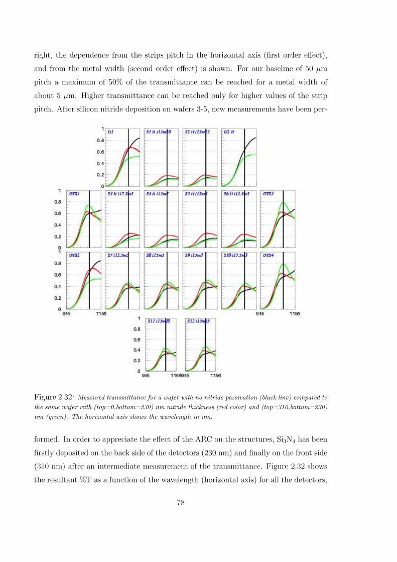
right, the dependence from the strips pitch in the horizontal axis (rst order eect),
and from the metal width (second order eect) is shown. For our baseline of 50 m
pitch a maximum of 50% of the transmittance can be reached for a metal width of
about 5 m. Higher transmittance can be reached only for higher values of the strip
pitch. After silicon nitride deposition on wafers 3-5, new measurements have been per-
Figure 2.32: Measured transmittance for a wafer with no nitride passivation (black line) compared to
the same wafer with (top=0,bottom=230) nm nitride thickness (red color) and (top=310,bottom=230)
nm (green). The horizontal axis shows the wavelength in nm.
formed. In order to appreciate the eect of the ARC on the structures, Si3N4 has been
rstly deposited on the back side of the detectors (230 nm) and nally on the front side
(310 nm) after an intermediate measurement of the transmittance. Figure 2.32 shows
the resultant %T as a function of the wavelength (horizontal axis) for all the detectors,
78
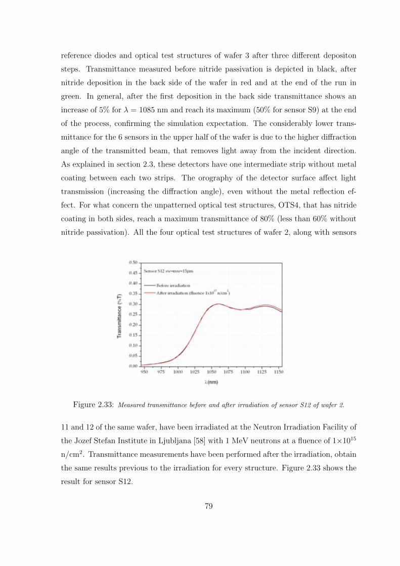
reference diodes and optical test structures of wafer 3 after three dierent depositon
steps. Transmittance measured before nitride passivation is depicted in black, after
nitride deposition in the back side of the wafer in red and at the end of the run in
green. In general, after the rst deposition in the back side transmittance shows an
increase of 5% for = 1085 nm and reach its maximum (50% for sensor S9) at the end
of the process, conrming the simulation expectation. The considerably lower trans-
mittance for the 6 sensors in the upper half of the wafer is due to the higher diraction
angle of the transmitted beam, that removes light away from the incident direction.
As explained in section 2.3, these detectors have one intermediate strip without metal
coating between each two strips. The orography of the detector surface aect light
transmission (increasing the diraction angle), even without the metal re ection ef-
fect. For what concern the unpatterned optical test structures, OTS4, that has nitride
coating in both sides, reach a maximum transmittance of 80% (less than 60% without
nitride passivation). All the four optical test structures of wafer 2, along with sensors
Figure 2.33: Measured transmittance before and after irradiation of sensor S12 of wafer 2.
11 and 12 of the same wafer, have been irradiated at the Neutron Irradiation Facility of
the Jozef Stefan Institute in Ljubljana [58] with 1 MeV neutrons at a uence of 11015
n/cm2. Transmittance measurements have been performed after the irradiation, obtain
the same results previous to the irradiation for every structure. Figure 2.33 shows the
result for sensor S12.
79

2.7 Summary and discussion
The aim of the work presented in this chapter was the development of new microstrip
detectors for the laser alignment systems of future particle trackers. It basically con-
sisted in the improvement of transmittance of the sensors to the IR light, changing the
values of key layout and technological parameters, but still using a standard fabrication
process.
An optical model of the sensor has been developed by the IFCA group of experi-
mental physics in Santander, and validated with the use of many test wafers produced
in the IMB-CNM clean room laboratories. The passage of a coherent beam of light
through the active volume of the detector has been simulated identifying the mini-
mum changes needed in the design and technology to maximize the transmittance.
The transmittance of a microstrip detector results to depend at the rst degree on
the periodicity of the strips. The lower the pitch, the higher the diraction angle and
the lower transmittance collected along the incoming propagation direction. With a
baseline pitch of 50 m, a metal-strip-width/pitch ratio 10%, together with a careful
choise of the thickness of the material layers, gave the highest transmittance value
(%T=50%).
The layout for the rst prototype detectors has been designed respecting simulation
hints. Mask design includes twelve baby sensors equipped with 256 readout strips with
a pitch of 50 m. A circular window (1 cm diameter) has been opened in the aluminium
backplane to allow the laser beam to pass through and the width of the aluminium
electrode and strip implant was varied from sensor to sensor within the wafer to study
the dependence of transmittance and electrical behaviours on these layout parameters.
Half of the detectors has also one intermediate implant within two readout strips, in
order to increase their spatial resolution. Many optical and electrical test structures
have been added to the mask.
The detectors have been fabricated using the standard ow of processes developed
by the IMB-CNM radiation detectors group for the fabrication of silicon microstrip
detectors and setting the processes parameters in order to obtain the material layers
thickness advised by the simulation. The real thickness and uniformity of each material
have been measured after each oxidation or deposition process: in general the values
obtained are in agreement with the ones expected and their uniformity within the wafer
80
surface is better than 5%, value required to ensure reproducibility of devices with the
same optical characteristics.
The electrical characterization of the samples demonstrates that the optimization
of the passivation layers does not aect their electrical behaviour, showing the expected
dependence of their characteristics on the layout parameters.
The detectors have been optically characterized with the use of a spectrophotome-
ter in the wavelength of interest at dierent stage of their fabrication. Measurement
results highlight the importance of the last passivation layer (silicon nitride) as an
anti-re ection coating (ARC), especially for what concern the passivation of the back
electrode window. Optical test structures with unpatterned surfaces reach a maximum
transmittance of 80%, while the detectors with strip (metal) width 15(3) m reach the
expected value of 50% at the end of the run, validating the simulation model of the
detector as a powerfull and correct tool. Detectors with intermediate strips without
metal coating show a considerably lower transmittance, revealing the strict in uence
on light diraction of the orography of the sensor surface. A further characterization
of some samples and test structures demonstrates that the transmittance value does
not change after irradiation with 1 MeV neutrons at a uence of 11015 n/cm2.
A transmittance value of 50% means that 5 consecutive modules can be aligned
with the same laser beam. Obtaining this result with a pitch of 50m is a very good
improvement with respect to previous versions of transparent detectors. For instance,
CMS obtained transmittance of 20% for a pitch of 189m. The comparison with AMS
is less direct, since the detectors are double sided, with crossed strips. For reference,
the maximum transmittance achieved there was 50% with a 110 m readout pitch in
one of the sides. Considering the simulation predictions, validated by the experimental
results, doubling the strip pitch in the sensors developed in this work, a transmittance
value close to 70% can be achieved, that translates into increasing the number of
modules that can be aligned of a factor 2.
Beam tests of some samples are in program for future characterizations in order
to test the detectors eciency and radiation hardness, especially for what concern the
prototypes with extremely slim metal strips.
81

82
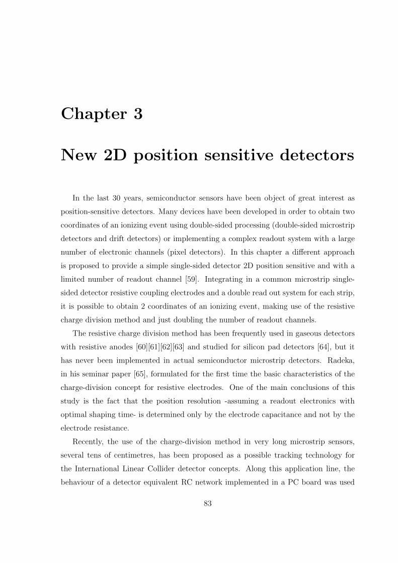
Chapter 3
New 2D position sensitive detectors
In the last 30 years, semiconductor sensors have been object of great interest as
position-sensitive detectors. Many devices have been developed in order to obtain two
coordinates of an ionizing event using double-sided processing (double-sided microstrip
detectors and drift detectors) or implementing a complex readout system with a large
number of electronic channels (pixel detectors). In this chapter a dierent approach
is proposed to provide a simple single-sided detector 2D position sensitive and with a
limited number of readout channel [59]. Integrating in a common microstrip single-
sided detector resistive coupling electrodes and a double read out system for each strip,
it is possible to obtain 2 coordinates of an ionizing event, making use of the resistive
charge division method and just doubling the number of readout channels.
The resistive charge division method has been frequently used in gaseous detectors
with resistive anodes [60][61][62][63] and studied for silicon pad detectors [64], but it
has never been implemented in actual semiconductor microstrip detectors. Radeka,
in his seminar paper [65], formulated for the rst time the basic characteristics of the
charge-division concept for resistive electrodes. One of the main conclusions of this
study is the fact that the position resolution -assuming a readout electronics with
optimal shaping time- is determined only by the electrode capacitance and not by the
electrode resistance.
Recently, the use of the charge-division method in very long microstrip sensors,
several tens of centimetres, has been proposed as a possible tracking technology for
the International Linear Collider detector concepts. Along this application line, the
behaviour of a detector equivalent RC network implemented in a PC board was used
83
for the benchmarking of a SPICE electronic circuit simulation [66]. The PC board
was populated with discrete components with electrical specications matching the
main electrical parameters of such long microstrip detector DC coupled to the readout
electronics. The simulation, supported by the RC network measurements, conrmed
the overall validity of Radeka's formulation on resistive charge-division.
(a) (b)
Figure 3.1: (a) Schematic top view of the novel detector and (b) lateral cross-section of the central
strip (not to scale). It is possible to distinguish the aluminium elements in blue and the resistive
electrodes on the strips (light yellow regions). The aluminium pads are connected each one to a channel
of the read-out electronics (two for each strip). When an ionizing particle crosses the detector, dierent
signals (S1 and S2) are read by the opposite electronic channels. The X coordinate of the event can be
reconstructed using the center of gravity method, whereas the Y coordinate is reconstructed comparing
the signal amplitudes at the ends of strips.
In this chapter, a novel microstrip detector concept is introduced, where the re-
sistive electrodes (light yellow structure in gure 3.1 (a) and (b)) are made of a thin
layer of highly doped polycrystalline silicon. This original approach decouples the re-
sistive electrodes from the detector diode structure (determining the charge collection)
through a coupling capacitance (gray layer in gure 3.1 (b)). In this way, it is easy to
manufacture AC coupled p+-on-n or n+-on-p detectors, more convenient for the case of
high radiation environments. The eld of application of this device expands beyond the
84

nuclear or particle physics tracking applications, reaching other possible areas as laser-
based position sensitive devices, heavy ion and other highly-ionizing particle detector,
Compton cameras, medical imaging, etc.
In the next sections, the feasibility of the resistive charge division concept in a
full- edged microstrip detector is demonstrated. Then, the rst results on the re-
construction of the hit position along the strip direction using the proof-of-concept
prototypes is presented. The experimental method used to this purpose was the study
of the output signals under a longitudinal scan of a strip, carried out with an infrared
laser beam.
3.1 Principle of operation: resistive charge division
in microstrip detectors
As seen in chapter 2, in a conventional microstrip detector the metal contacts of
the strips extend over almost all the length of the implants and are connected each
one to a read-out channel. When an ionizing particle crosses the detector, the prop-
agation of the induced signal along the coupling electrode does not suer signicant
attenuation, i.e., the signal amplitude does not depend on the particle impinging point
along the electrode direction. When using, instead of metal alloy, a resistive coupling
electrode equipped with metal contacts at its ends, the signal undergoes signicant
attenuation during its propagation towards the electronics contacts. The longer the
propagation length, the larger the signal attenuation. In this way, a conventionally
manufactured single-sided microstrip sensor can provide the two-dimensional coordi-
nates of the particle impinging point; the transverse coordinate derived from the usual
electrode segmentation [15] and the longitudinal coordinate determined by relating
signals amplitude at both ends of the electrode.
The resistive electrode represents a diusive RC line, in which a current pulse un-
dergoes not only an amplitude attenuation but also an increase of the rise time the
further it travels. Using readout electronics characterized by a short -compared to
the RC constant of the line- shaping time, this translates into a non constant signal
ballistic decit (see section 1.3.3). The ballistic decit can be reduced increasing the
shaper peaking time; however, a longer peaking time increases the parallel readout
85

noise contribution (section 1.3.2). In reference [65], Radeka derived the optimal peak-
ing time for a resistive charge division conguration, under the assumption of high
electrode resistance compared to the amplier impedance and long amplier peaking
time compared to input signal rise times.
Under these assumptions, dependence between the longitudinal coordinate of the
particle position and the fractional signal amplitude read from one side of the strip is
expected to be linear. The actual functional form (following gure 3.1 notation with
A1 and A2 the amplitudes of S1 and S2 respectively) is given by equation 3.1:
y = L A2
A1 + A2
(3.1)
3.2 Proof-of-concept prototypes
3.2.1 Specications and fabrication
The resistive charge-division proof-of-concept prototypes presented here are AC
coupled microstrip detectors with the upper electrodes of the coupling capacitor made
of polycrystalline silicon. Two prototypes with dierent electrode resistivity were fab-
ricated at the IMB-CNM clean room facilities in Barcelona, using the standard tech-
nology for single-sided p+-on-n, AC coupled, silicon microstrip detectors (see mask
levels sequence in section 2.3). A standard reference sensor and several electrical test
structures [51] were included in each wafer of the fabrication run that allowed a more
direct measurement of the electrical parameters of the new sensors.
Each detector consists of 384 p+ strips (20 m wide) with a pitch of 80 m on
a (28515) m thick n-type substrate. The resistive electrodes (30 m wide) have a
total length of 2 cm with linear resistance R=l=2.8 =m for one of the devices and
R=l=12.2 =m for the other. The linear resistances have been dened during the
processes ow dedicated to the bias resistors formation. As introduced in section 2.4.5,
after the ion implantation processes used to create the strips and a general cleaning
treatment, 600 nm of polysilicon is deposited by means of a LPCVD process. To
better understand the electrodes formation, a lateral cross section of the detector (like
in gure 3.1 (b)) is depicted in gures 3.2 and 3.3, under the processes ow of interest.
After polysilicon deposition (b) a Boron implantation process (c) is used to dene its
86

resistivity. Then a first photolithography process (d) is used to transfer the patterns to
Figure 3.2: First steps for the polysilicon electrodes (and bias resistors) definition. Theschematics refers to a detail of a lateral cross section of the detector as in figure 3.1 (b).Drawing not in scale.
Figure 3.3: Final steps for the polysilicon electrodes (and bias resistors) definition and final result
of the processing.
87

the photoresist for a selective ion (Boron) implantation (e) at both ends of the resistors,
in order to further reduce the resistivity of polysilicon in the connections between the
resistors edges and the metal contacts and, at the same time, to select the R/ of the
electrodes. As the nal dopant concentration is controlled by the doses and energy of
the ions as well as by the duration of the process, the two dierent R/ values have been
obtained changing these parameters from wafer to wafer. A second photolithography
process (g) then denes the resistors and the electrodes shape. A nal cleaning and
thermal treatment at 950C (l) is necessary for the dopants diusion, crystals size
enlargement and the preparation of the wafer for the next processes involving contact
formation and passivation of the device. The nal result can be seen in the bottom of
gure 3.3. In particular it is possible to appreciate the metallization of the bias ring
(with the pad for the wire bonding to the bias circuit), the DC pad of the strip (via
opened through the oxide layer) useful for the electrical characterization of the sensor
and the metal pads at the two ends of the polysilicon electrode for the connection with
the readout electronics.
3.2.2 Modelling and simulation of the detector
A SPICE-like model of each prototype and the readout electronics have been de-
veloped in order to clarify the possible eect of the non-optimal shaping time on the
linearity of equation 3.1, studying the response of the detector to a simulated current
pulse injected at dierent points along the strip length.
Starting from the work presented in reference [69] the model of our detector has
been built with standard components from the AnalogLib library of Virtuoso Spectre
by Cadence [70]. A portion of the detector including ve consecutive strips is modelled
by a periodic structure composed of 80 cells, each one corresponding to a transverse
section (250 m long) of the strips. The unit cell is a complex chain of capacitances and
resistors representing the main electrical characteristics of the device as the substrate
resistance and capacitance (Rsub and Csub), the interstrip resistance and capacitance
(Rint and Cint), the p+implant resistance (Rimpl), the coupling capacitance (CAC) and
the resistance of the resistive upper electrode (Rel). Figure 3.4 shows the schematic
of the unit cell. The values of the circuital elements have been determined from the
ones measured during the electrical characterization of the detectors in full depletion
88
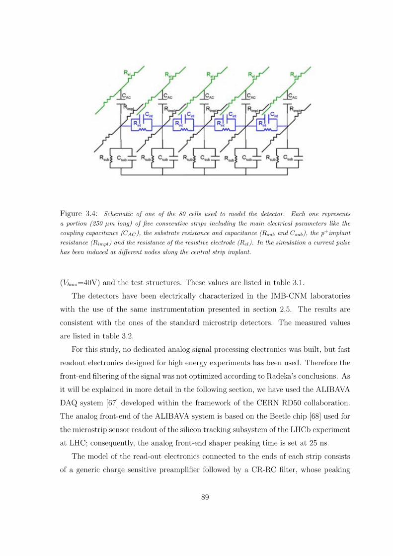
Figure 3.4: Schematic of one of the 80 cells used to model the detector. Each one represents
a portion (250 m long) of ve consecutive strips including the main electrical parameters like the
coupling capacitance (CAC), the substrate resistance and capacitance (Rsub and Csub), the p+implant
resistance (Rimpl) and the resistance of the resistive electrode (Rel). In the simulation a current pulse
has been induced at dierent nodes along the central strip implant.
(Vbias=40V) and the test structures. These values are listed in table 3.1.
The detectors have been electrically characterized in the IMB-CNM laboratories
with the use of the same instrumentation presented in section 2.5. The results are
consistent with the ones of the standard microstrip detectors. The measured values
are listed in table 3.2.
For this study, no dedicated analog signal processing electronics was built, but fast
readout electronics designed for high energy experiments has been used. Therefore the
front-end ltering of the signal was not optimized according to Radeka's conclusions. As
it will be explained in more detail in the following section, we have used the ALIBAVA
DAQ system [67] developed within the framework of the CERN RD50 collaboration.
The analog front-end of the ALIBAVA system is based on the Beetle chip [68] used for
the microstrip sensor readout of the silicon tracking subsystem of the LHCb experiment
at LHC; consequently, the analog front-end shaper peaking time is set at 25 ns.
The model of the read-out electronics connected to the ends of each strip consists
of a generic charge sensitive preamplier followed by a CR-RC lter, whose peaking
89
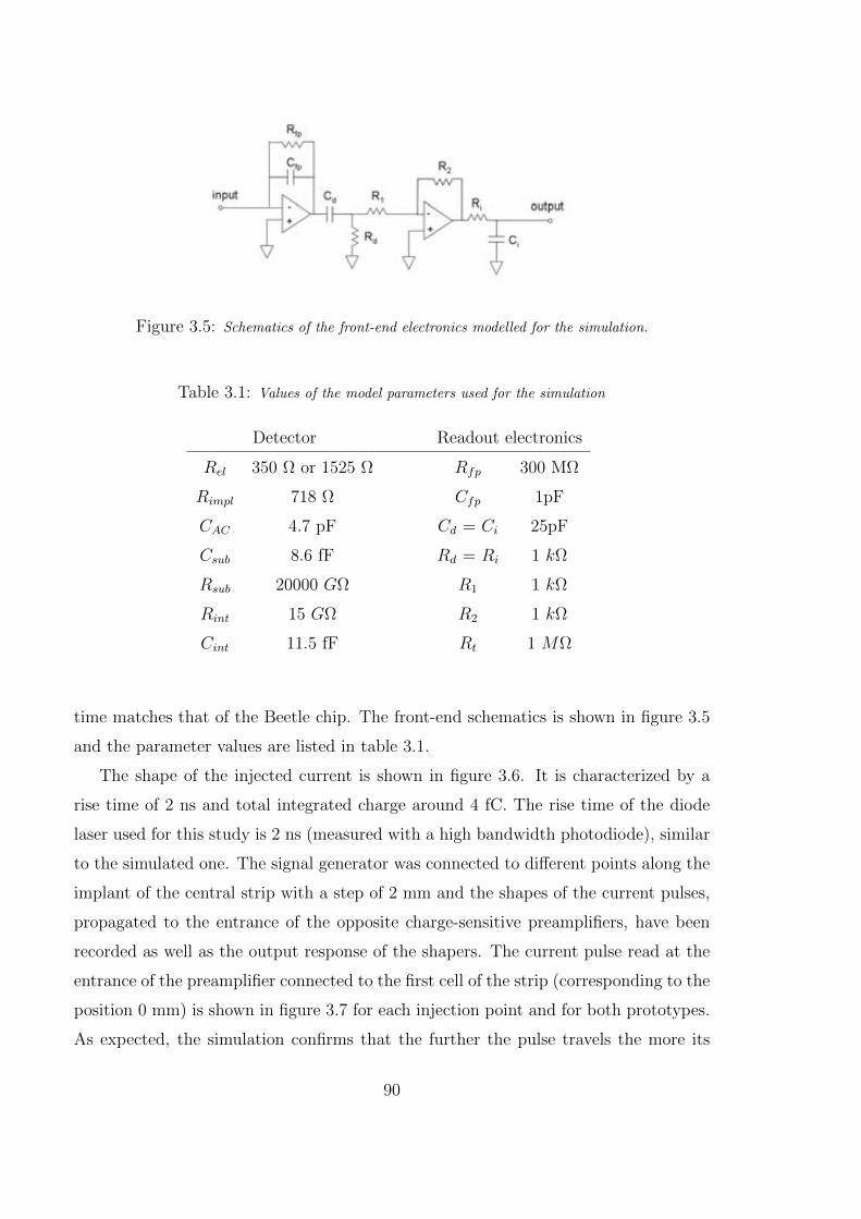
Figure 3.5: Schematics of the front-end electronics modelled for the simulation.
Table 3.1: Values of the model parameters used for the simulation
Detector Readout electronics
Rel 350 or 1525 Rfp 300 M
Rimpl 718 Cfp 1pF
CAC 4.7 pF Cd = Ci 25pF
Csub 8.6 fF Rd = Ri 1 k
Rsub 20000 G R1 1 k
Rint 15 G R2 1 k
Cint 11.5 fF Rt 1 M
time matches that of the Beetle chip. The front-end schematics is shown in gure 3.5
and the parameter values are listed in table 3.1.
The shape of the injected current is shown in gure 3.6. It is characterized by a
rise time of 2 ns and total integrated charge around 4 fC. The rise time of the diode
laser used for this study is 2 ns (measured with a high bandwidth photodiode), similar
to the simulated one. The signal generator was connected to dierent points along the
implant of the central strip with a step of 2 mm and the shapes of the current pulses,
propagated to the entrance of the opposite charge-sensitive preampliers, have been
recorded as well as the output response of the shapers. The current pulse read at the
entrance of the preamplier connected to the rst cell of the strip (corresponding to the
position 0 mm) is shown in gure 3.7 for each injection point and for both prototypes.
As expected, the simulation conrms that the further the pulse travels the more its
90
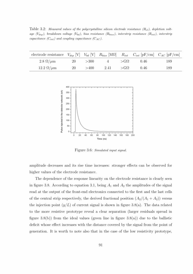
Table 3.2: Measured values of the polycrystalline silicon electrode resistance (Rel), depletion volt-
age (Vdep), breakdown voltage (Vbd), bias resistance (Rbias), interstrip resistance (Rint), interstrip
capacitance (Cint) and coupling capacitance (CAC).
electrode resistance Vdep [V] Vbd [V] Rbias [M] Rint Cint [pF/cm] CAC [pF/cm]
2.8 /m 20 >300 4 >G 0.46 189
12.2 /m 20 >400 2.41 >G 0.46 189
Figure 3.6: Simulated input signal.
amplitude decreases and its rise time increases: stronger eects can be observed for
higher values of the electrode resistance.
The dependence of the response linearity on the electrode resistance is clearly seen
in gure 3.8. According to equation 3.1, being A1 and A2 the amplitudes of the signal
read at the output of the front-end electronics connected to the rst and the last cells
of the central strip respectively, the derived fractional position (A2=(A1 + A2)) versus
the injection point (y=L) of current signal is shown in gure 3.8(a). The data related
to the more resistive prototype reveal a clear separation (larger residuals spread in
gure 3.8(b)) from the ideal values (green line in gure 3.8(a)) due to the ballistic
decit whose eect increases with the distance covered by the signal from the point of
generation. It is worth to note also that in the case of the low resistivity prototype,
91
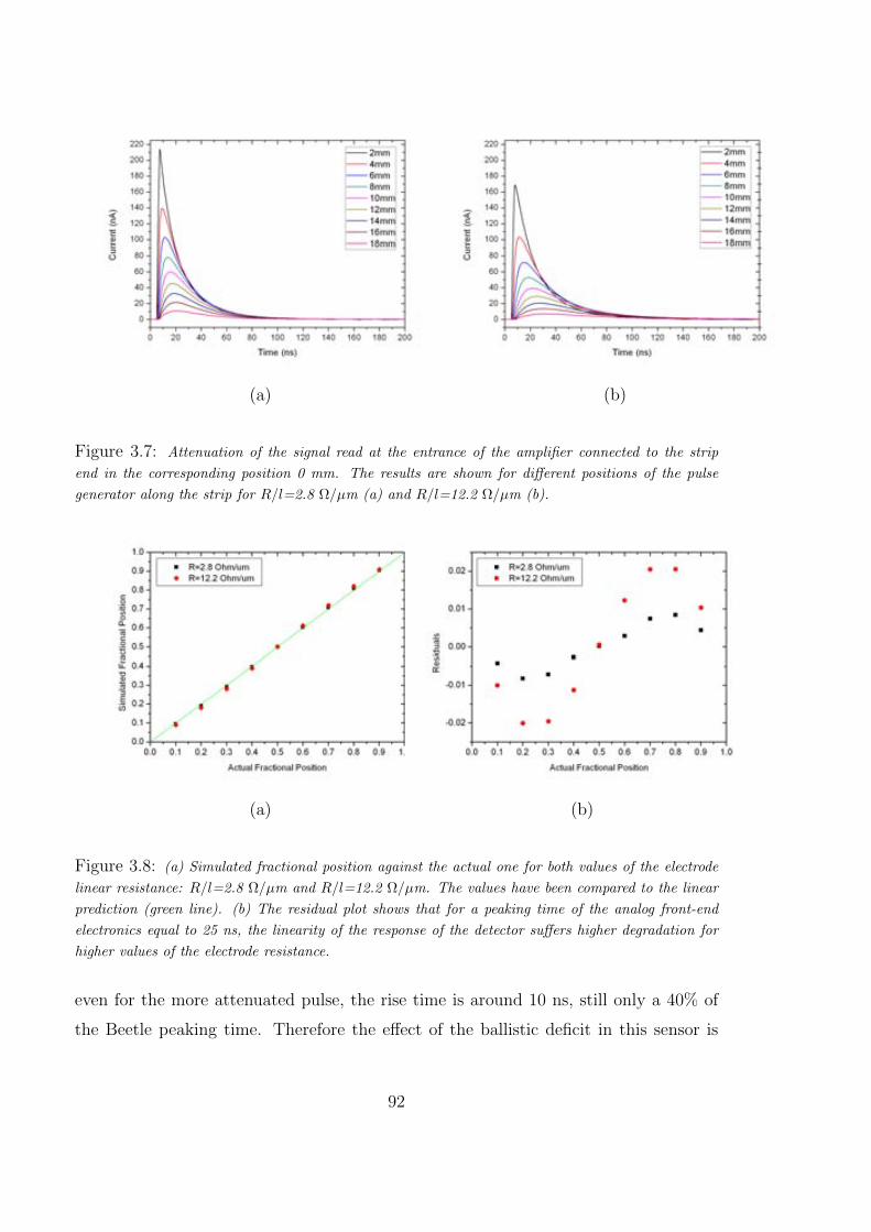
(a) (b)
Figure 3.7: Attenuation of the signal read at the entrance of the amplier connected to the strip
end in the corresponding position 0 mm. The results are shown for dierent positions of the pulse
generator along the strip for R=l=2.8 Ω=m (a) and R=l=12.2 Ω=m (b).
(a) (b)
Figure 3.8: (a) Simulated fractional position against the actual one for both values of the electrode
linear resistance: R=l=2.8 Ω=m and R=l=12.2 Ω=m. The values have been compared to the linear
prediction (green line). (b) The residual plot shows that for a peaking time of the analog front-end
electronics equal to 25 ns, the linearity of the response of the detector suers higher degradation for
higher values of the electrode resistance.
even for the more attenuated pulse, the rise time is around 10 ns, still only a 40% of
the Beetle peaking time. Therefore the eect of the ballistic decit in this sensor is
92
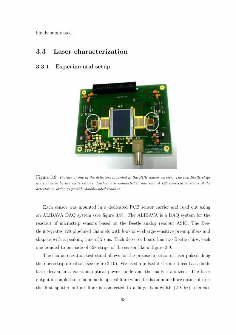
highly suppressed.
3.3 Laser characterization
3.3.1 Experimental setup
Figure 3.9: Picture of one of the detectors mounted in the PCB sensor carrier. The two Beetle chips
are indicated by the white circles. Each one is connected to one side of 128 consecutive strips of the
detector in order to provide double-sided readout.
Each sensor was mounted in a dedicated PCB sensor carrier and read out using
an ALIBAVA DAQ system (see gure 3.9). The ALIBAVA is a DAQ system for the
readout of microstrip sensors based on the Beetle analog readout ASIC. The Bee-
tle integrates 128 pipelined channels with low-noise charge-sensitive preampliers and
shapers with a peaking time of 25 ns. Each detector board has two Beetle chips, each
one bonded to one side of 128 strips of the sensor like in gure 3.9.
The characterization test-stand allows for the precise injection of laser pulses along
the microstrip direction (see gure 3.10). We used a pulsed distributed-feedback diode
laser driven in a constant optical power mode and thermally stabilized. The laser
output is coupled to a monomode optical bre which feeds an inline bre optic splitter:
the rst splitter output bre is connected to a large bandwidth (2 Ghz) reference
93
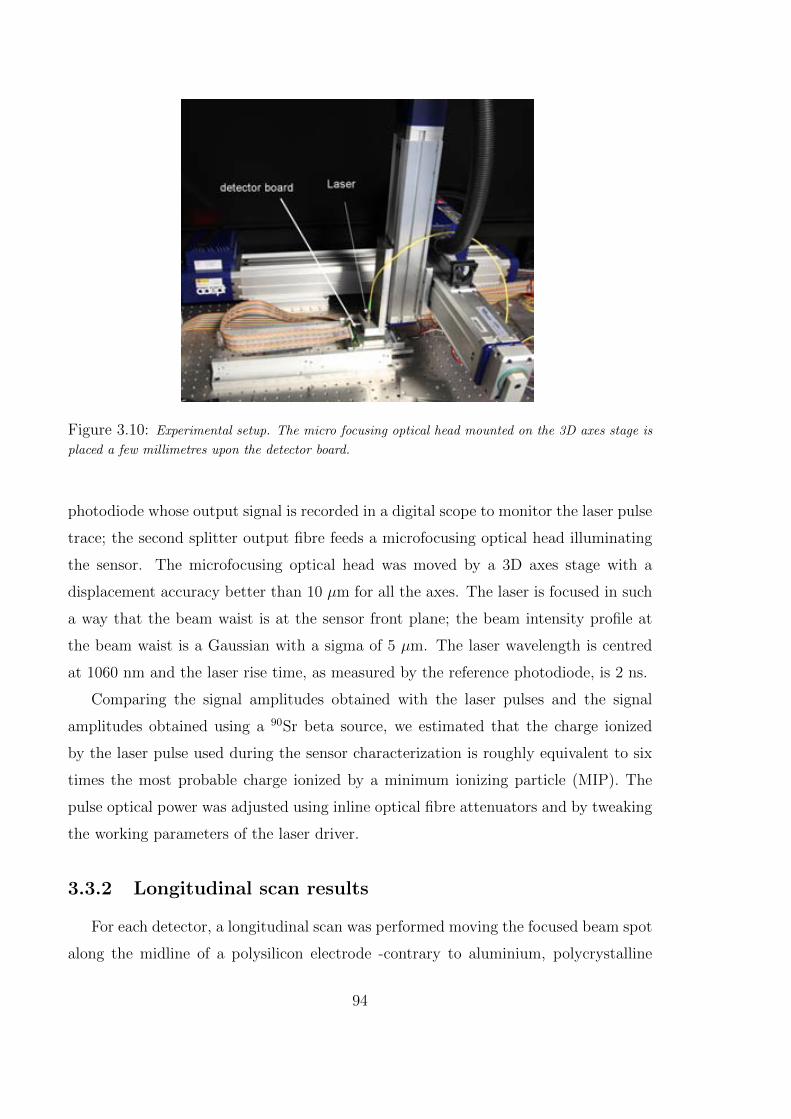
Figure 3.10: Experimental setup. The micro focusing optical head mounted on the 3D axes stage is
placed a few millimetres upon the detector board.
photodiode whose output signal is recorded in a digital scope to monitor the laser pulse
trace; the second splitter output bre feeds a microfocusing optical head illuminating
the sensor. The microfocusing optical head was moved by a 3D axes stage with a
displacement accuracy better than 10 m for all the axes. The laser is focused in such
a way that the beam waist is at the sensor front plane; the beam intensity prole at
the beam waist is a Gaussian with a sigma of 5 m. The laser wavelength is centred
at 1060 nm and the laser rise time, as measured by the reference photodiode, is 2 ns.
Comparing the signal amplitudes obtained with the laser pulses and the signal
amplitudes obtained using a 90Sr beta source, we estimated that the charge ionized
by the laser pulse used during the sensor characterization is roughly equivalent to six
times the most probable charge ionized by a minimum ionizing particle (MIP). The
pulse optical power was adjusted using inline optical bre attenuators and by tweaking
the working parameters of the laser driver.
3.3.2 Longitudinal scan results
For each detector, a longitudinal scan was performed moving the focused beam spot
along the midline of a polysilicon electrode -contrary to aluminium, polycrystalline
94
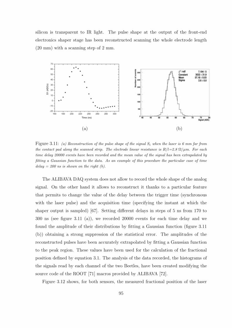
silicon is transparent to IR light. The pulse shape at the output of the front-end
electronics shaper stage has been reconstructed scanning the whole electrode length
(20 mm) with a scanning step of 2 mm.
(a) (b)
Figure 3.11: (a) Reconstruction of the pulse shape of the signal S1 when the laser is 6 mm far from
the contact pad along the scanned strip. The electrode linear resistance is R=l=2.8 Ω=m. For each
time delay 20000 events have been recorded and the mean value of the signal has been extrapolated by
tting a Gaussian function to the data. As an example of this procedure the particular case of time
delay = 200 ns is shown on the right (b).
The ALIBAVA DAQ system does not allow to record the whole shape of the analog
signal. On the other hand it allows to reconstruct it thanks to a particular feature
that permits to change the value of the delay between the trigger time (synchronous
with the laser pulse) and the acquisition time (specifying the instant at which the
shaper output is sampled) [67]. Setting dierent delays in steps of 5 ns from 170 to
300 ns (see gure 3.11 (a)), we recorded 20000 events for each time delay and we
found the amplitude of their distributions by tting a Gaussian function (gure 3.11
(b)) obtaining a strong suppression of the statistical error. The amplitudes of the
reconstructed pulses have been accurately extrapolated by tting a Gaussian function
to the peak region. These values have been used for the calculation of the fractional
position dened by equation 3.1. The analysis of the data recorded, the histograms of
the signals read by each channel of the two Beetles, have been created modifying the
source code of the ROOT [71] macros provided by ALIBAVA [72].
Figure 3.12 shows, for both sensors, the measured fractional position of the laser
95
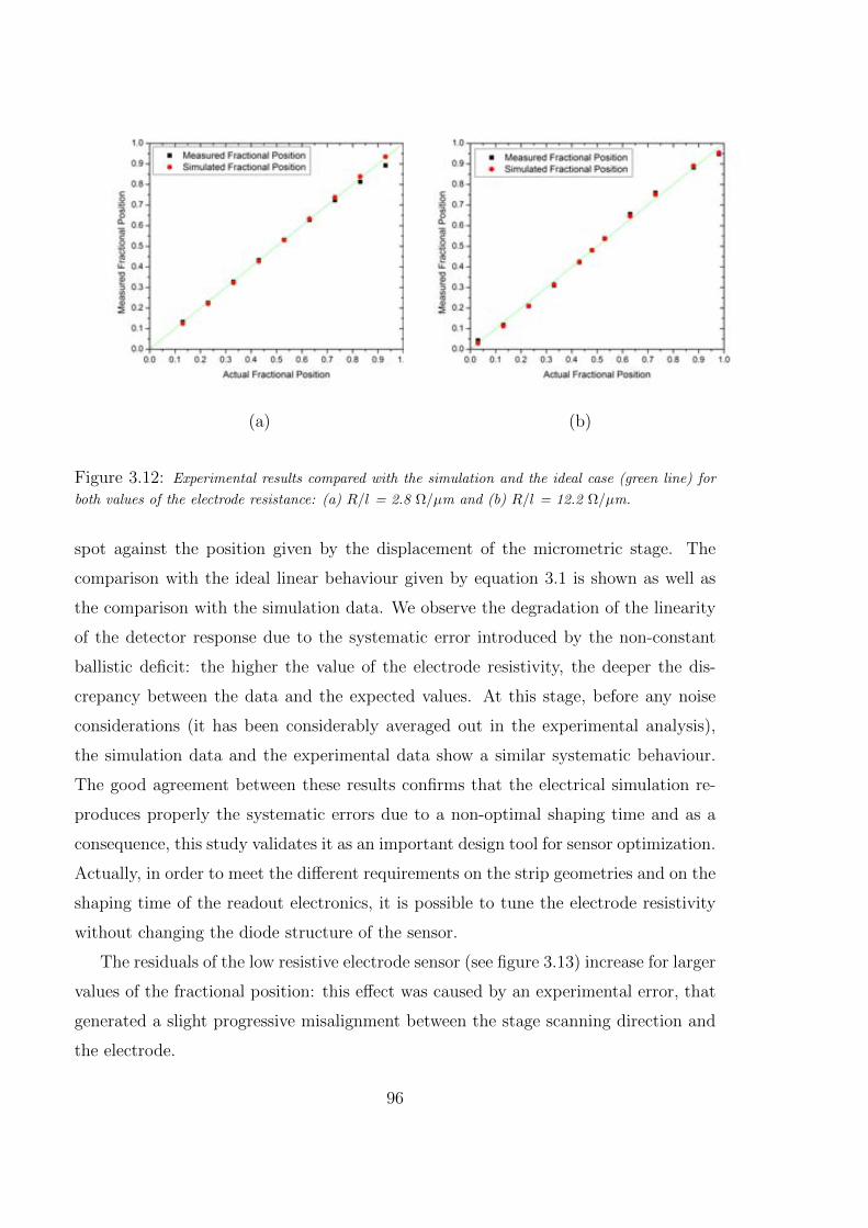
(a) (b)
Figure 3.12: Experimental results compared with the simulation and the ideal case (green line) for
both values of the electrode resistance: (a) R=l = 2.8 Ω=m and (b) R=l = 12.2 Ω=m.
spot against the position given by the displacement of the micrometric stage. The
comparison with the ideal linear behaviour given by equation 3.1 is shown as well as
the comparison with the simulation data. We observe the degradation of the linearity
of the detector response due to the systematic error introduced by the non-constant
ballistic decit: the higher the value of the electrode resistivity, the deeper the dis-
crepancy between the data and the expected values. At this stage, before any noise
considerations (it has been considerably averaged out in the experimental analysis),
the simulation data and the experimental data show a similar systematic behaviour.
The good agreement between these results conrms that the electrical simulation re-
produces properly the systematic errors due to a non-optimal shaping time and as a
consequence, this study validates it as an important design tool for sensor optimization.
Actually, in order to meet the dierent requirements on the strip geometries and on the
shaping time of the readout electronics, it is possible to tune the electrode resistivity
without changing the diode structure of the sensor.
The residuals of the low resistive electrode sensor (see gure 3.13) increase for larger
values of the fractional position: this eect was caused by an experimental error, that
generated a slight progressive misalignment between the stage scanning direction and
the electrode.
96
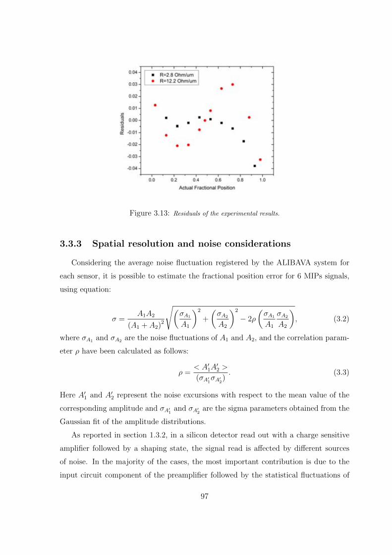
Figure 3.13: Residuals of the experimental results.
3.3.3 Spatial resolution and noise considerations
Considering the average noise uctuation registered by the ALIBAVA system for
each sensor, it is possible to estimate the fractional position error for 6 MIPs signals,
using equation:
=A1A2
(A1 + A2)2
√(A1
A1
)2
+
(A2
A2
)2
2
(A1
A1
A2
A2
); (3.2)
where A1 and A2 are the noise uctuations of A1 and A2, and the correlation param-
eter have been calculated as follows:
=< A01A
02 >
(A′1A′
2): (3.3)
Here A01 and A02 represent the noise excursions with respect to the mean value of the
corresponding amplitude and A′1
and A′2
are the sigma parameters obtained from the
Gaussian t of the amplitude distributions.
As reported in section 1.3.2, in a silicon detector read out with a charge sensitive
amplier followed by a shaping state, the signal read is aected by dierent sources
of noise. In the majority of the cases, the most important contribution is due to the
input circuit component of the preamplier followed by the statistical uctuations of
97

the leakage current (shot noise). In this type of detectors, the thermal noise due to the
resistive electrode has also to be considered: it can be represented by a current source
in parallel with the input, with average intensity proportional to 1/R and a frequency
independent spectrum [65], [73]. Any other noise source is negligible in this context.
Each source contributes to the value of and in a dierent way. Remember that
can assume values in the range (-1;1), where = 1 represents full anti-correlation,
= 1 full correlation and = 0 represents uncorrelation.
The amplier noise is associated to the input transistor of the amplier, therefore,
considering both channels of an electrode, it is uncorrelated and one should expect of
similar amplitudes, when using similar electronics at both ends; under this assumptions
this noise parameters are:
A1 ' A2; = 0 (3.4)
Making explicit the dependence on the fractional position of the laser impinging
point x = A2=(A1 + A2) in equation 3.1, one obtain:
2x =
1
(A1 + A2)2[(L x)22
2 2x(L x)12 + x221] (3.5)
And in combination with equations 3.4:
(Ampx )2 =1
(A1 + A2)2[(L x)22
A2 + x22A1] (3.6)
Thus, the contribution of each amplier to the position resolution is higher when
the distance to the impinging point is higher. Total contribution should follow the
geometrical symmetry with respect to the centre of the strip.
The statistical uctuations of the leakage current is fully correlated if we assume
that both ends should sense the same increase or decrease of the leakage current; besides
the current excursions at both ends should be the same by symmetry. Under these two
assumptions we get the following noise parameters:
A1A2
= 1; = 1 (3.7)
Applying these parameter to equation 3.5 we get:
(Shotx )2 =1
(A1 + A2)2[(L x)A2 xA1]2 =
2A
(A1 + A2)2(L 2x)2 (3.8)
Thus the shot noise introduces a quadratic dependence with the position of the laser,
being zero at the centre of the electrode and maximal at the edges.
98
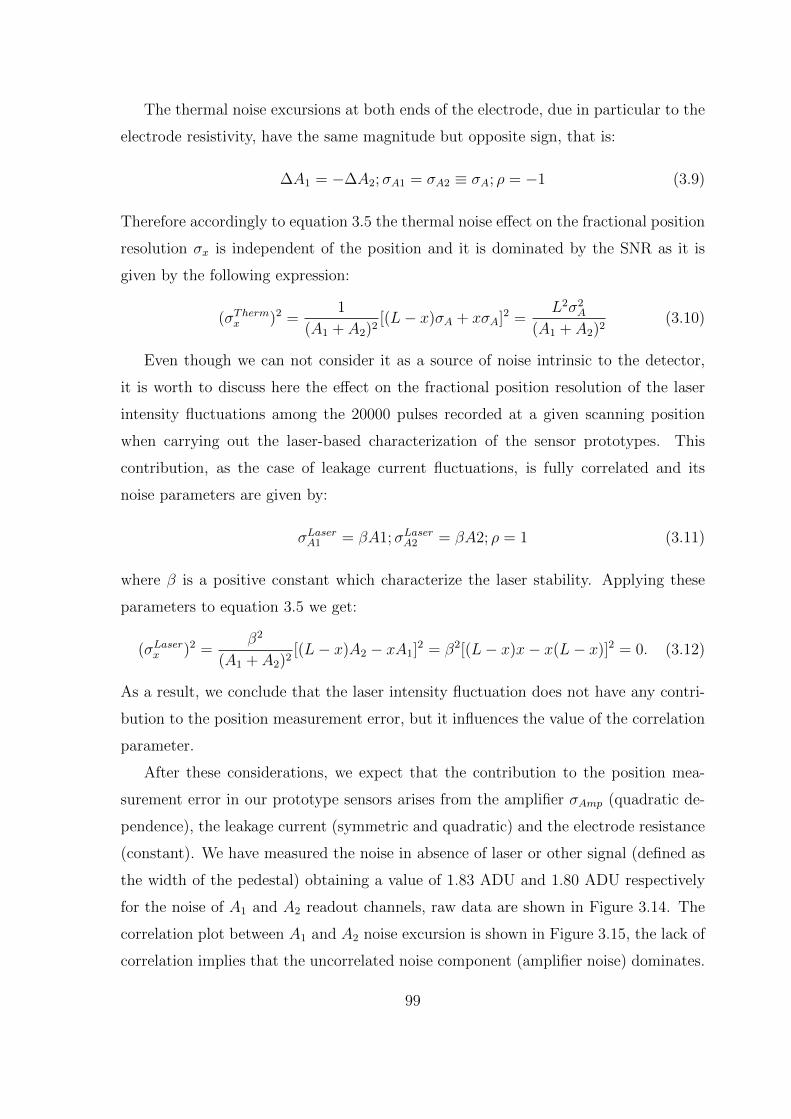
The thermal noise excursions at both ends of the electrode, due in particular to the
electrode resistivity, have the same magnitude but opposite sign, that is:
A1 = A2;A1 = A2 A; = 1 (3.9)
Therefore accordingly to equation 3.5 the thermal noise eect on the fractional position
resolution x is independent of the position and it is dominated by the SNR as it is
given by the following expression:
(Thermx )2 =1
(A1 + A2)2[(L x)A + xA]2 =
L22A
(A1 + A2)2(3.10)
Even though we can not consider it as a source of noise intrinsic to the detector,
it is worth to discuss here the eect on the fractional position resolution of the laser
intensity uctuations among the 20000 pulses recorded at a given scanning position
when carrying out the laser-based characterization of the sensor prototypes. This
contribution, as the case of leakage current uctuations, is fully correlated and its
noise parameters are given by:
LaserA1 = A1; LaserA2 = A2; = 1 (3.11)
where is a positive constant which characterize the laser stability. Applying these
parameters to equation 3.5 we get:
(Laserx )2 =2
(A1 + A2)2[(L x)A2 xA1]
2 = 2[(L x)x x(L x)]2 = 0: (3.12)
As a result, we conclude that the laser intensity uctuation does not have any contri-
bution to the position measurement error, but it in uences the value of the correlation
parameter.
After these considerations, we expect that the contribution to the position mea-
surement error in our prototype sensors arises from the amplier Amp (quadratic de-
pendence), the leakage current (symmetric and quadratic) and the electrode resistance
(constant). We have measured the noise in absence of laser or other signal (dened as
the width of the pedestal) obtaining a value of 1.83 ADU and 1.80 ADU respectively
for the noise of A1 and A2 readout channels, raw data are shown in Figure 3.14. The
correlation plot between A1 and A2 noise excursion is shown in Figure 3.15, the lack of
correlation implies that the uncorrelated noise component (amplier noise) dominates.
99

Figure 3.14: Raw distribution of pedestals
Figure 3.15: Simultaneous Noise excursion between the opposite ends of the same elec-trode in absence of laser pulse. Correlation parameter is 0.03.
100
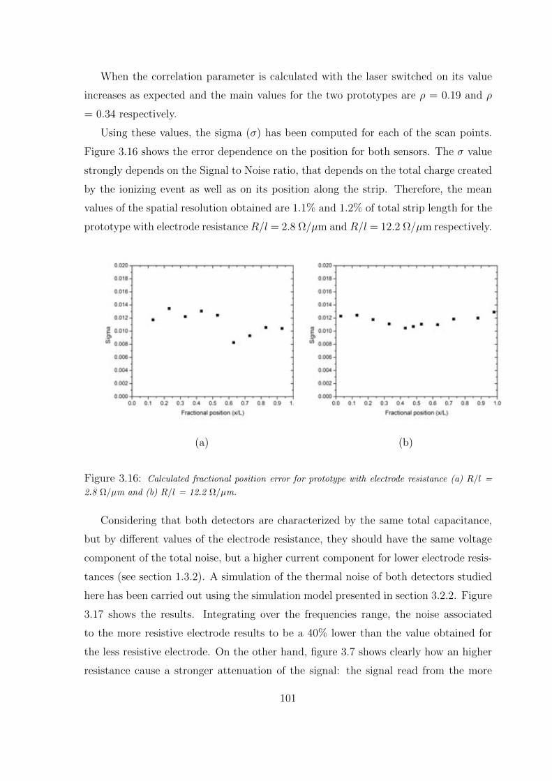
When the correlation parameter is calculated with the laser switched on its value
increases as expected and the main values for the two prototypes are = 0.19 and
= 0.34 respectively.
Using these values, the sigma () has been computed for each of the scan points.
Figure 3.16 shows the error dependence on the position for both sensors. The value
strongly depends on the Signal to Noise ratio, that depends on the total charge created
by the ionizing event as well as on its position along the strip. Therefore, the mean
values of the spatial resolution obtained are 1.1% and 1.2% of total strip length for the
prototype with electrode resistance R=l = 2.8 =m and R=l = 12.2 =m respectively.
(a) (b)
Figure 3.16: Calculated fractional position error for prototype with electrode resistance (a) R=l =
2.8 Ω=m and (b) R=l = 12.2 Ω=m.
Considering that both detectors are characterized by the same total capacitance,
but by dierent values of the electrode resistance, they should have the same voltage
component of the total noise, but a higher current component for lower electrode resis-
tances (see section 1.3.2). A simulation of the thermal noise of both detectors studied
here has been carried out using the simulation model presented in section 3.2.2. Figure
3.17 shows the results. Integrating over the frequencies range, the noise associated
to the more resistive electrode results to be a 40% lower than the value obtained for
the less resistive electrode. On the other hand, gure 3.7 shows clearly how an higher
resistance cause a stronger attenuation of the signal: the signal read from the more
101
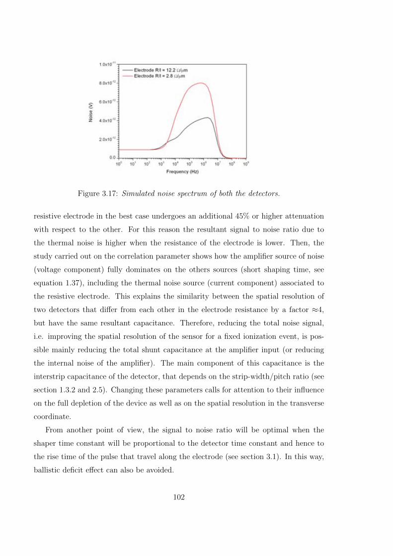
Figure 3.17: Simulated noise spectrum of both the detectors.
resistive electrode in the best case undergoes an additional 45% or higher attenuation
with respect to the other. For this reason the resultant signal to noise ratio due to
the thermal noise is higher when the resistance of the electrode is lower. Then, the
study carried out on the correlation parameter shows how the amplier source of noise
(voltage component) fully dominates on the others sources (short shaping time, see
equation 1.37), including the thermal noise source (current component) associated to
the resistive electrode. This explains the similarity between the spatial resolution of
two detectors that dier from each other in the electrode resistance by a factor 4,
but have the same resultant capacitance. Therefore, reducing the total noise signal,
i.e. improving the spatial resolution of the sensor for a xed ionization event, is pos-
sible mainly reducing the total shunt capacitance at the amplier input (or reducing
the internal noise of the amplier). The main component of this capacitance is the
interstrip capacitance of the detector, that depends on the strip-width/pitch ratio (see
section 1.3.2 and 2.5). Changing these parameters calls for attention to their in uence
on the full depletion of the device as well as on the spatial resolution in the transverse
coordinate.
From another point of view, the signal to noise ratio will be optimal when the
shaper time constant will be proportional to the detector time constant and hence to
the rise time of the pulse that travel along the electrode (see section 3.1). In this way,
ballistic decit eect can also be avoided.
102
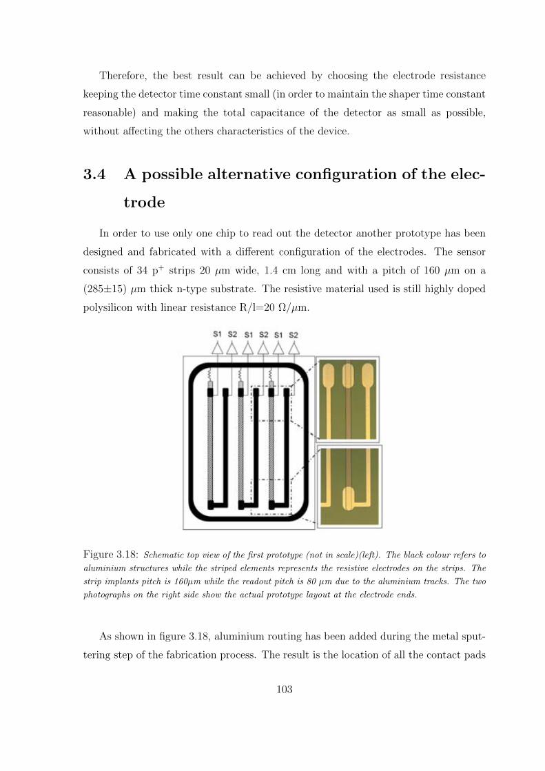
Therefore, the best result can be achieved by choosing the electrode resistance
keeping the detector time constant small (in order to maintain the shaper time constant
reasonable) and making the total capacitance of the detector as small as possible,
without aecting the others characteristics of the device.
3.4 A possible alternative conguration of the elec-
trode
In order to use only one chip to read out the detector another prototype has been
designed and fabricated with a dierent conguration of the electrodes. The sensor
consists of 34 p+ strips 20 m wide, 1.4 cm long and with a pitch of 160 m on a
(28515) m thick n-type substrate. The resistive material used is still highly doped
polysilicon with linear resistance R=l=20 =m.
Figure 3.18: Schematic top view of the rst prototype (not in scale)(left). The black colour refers to
aluminium structures while the striped elements represents the resistive electrodes on the strips. The
strip implants pitch is 160m while the readout pitch is 80 m due to the aluminium tracks. The two
photographs on the right side show the actual prototype layout at the electrode ends.
As shown in gure 3.18, aluminium routing has been added during the metal sput-
tering step of the fabrication process. The result is the location of all the contact pads
103

in the same region of the detector surface, that allows their connection to the channels
of only one readout chip.
The results of the electrical characterization of the prototype are still consistent with
the ones obtained by standard detectors: the measured values are listed in table 3.3.
Table 3.3: Measured values of the polycrystalline silicon electrode resistance (Rel), depletion volt-
age (Vdep), breakdown voltage (Vbd), bias resistance (Rbias), interstrip resistance (Rint), interstrip
capacitance (Cint) and coupling capacitance (CAC).
strip width Vdep Vbd Rbias Rint Cint CAC R
m [V] [V] [M] [pF/cm] [pF/cm] [=m]
20 40 >400 1.31 >G 0,6 173 20
As done for the other prototypes, the performances of this alternative detector have
been simulated with Spectre. The same model of the front-end electronics as well as
the same current pulse has been used. The detector model was composed of 56 cells
identical to the one represented in gure 3.4 with the values of the parameters listed
in table 3.4.
Table 3.4: List of the values of the model parameters.
Rel Rimpl CAC Csub Rsub Rint Cint
2500 800 3.43 pF 16.6 fF 20000 G 15 G 24 fF
The aluminium routing system has not been included in the model in order to
study their eects on the detector performance comparing the simulation with the
experimental results. The simulated fractional position A2=(A1 + A2) of the pulse
generator is shown in gure 3.19 as a function of the actual fractional position (y/L).
The well known eect of the ballistic decit on the detector response linearity is
pointed up by comparing the simulated data with the prediction of equation 3.1 (green
line).
The detector has been wire bonded to one Beetle chip of the daughter board of
the Alibava DAQ system and a longitudinal scan of one strip has been performed
104
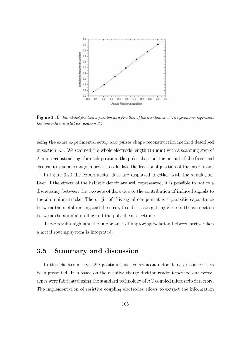
Figure 3.19: Simulated fractional position as a function of the nominal one. The green line represents
the linearity predicted by equation 2.1.
using the same experimental setup and pulses shape reconstruction method described
in section 3.3. We scanned the whole electrode length (14 mm) with a scanning step of
2 mm, reconstructing, for each position, the pulse shape at the output of the front-end
electronics shapers stage in order to calculate the fractional position of the laser beam.
In gure 3.20 the experimental data are displayed together with the simulation.
Even if the eects of the ballistic decit are well represented, it is possible to notice a
discrepancy between the two sets of data due to the contribution of induced signals to
the aluminium tracks. The origin of this signal component is a parasitic capacitance
between the metal routing and the strip, this decreases getting close to the connection
between the aluminium line and the polysilicon electrode.
These results highlight the importance of improving isolation between strips when
a metal routing system is integrated.
3.5 Summary and discussion
In this chapter a novel 2D position-sensitive semiconductor detector concept has
been presented. It is based on the resistive charge-division readout method and proto-
types were fabricated using the standard technology of AC coupled microstrip detectors.
The implementation of resistive coupling electrodes allows to extract the information
105
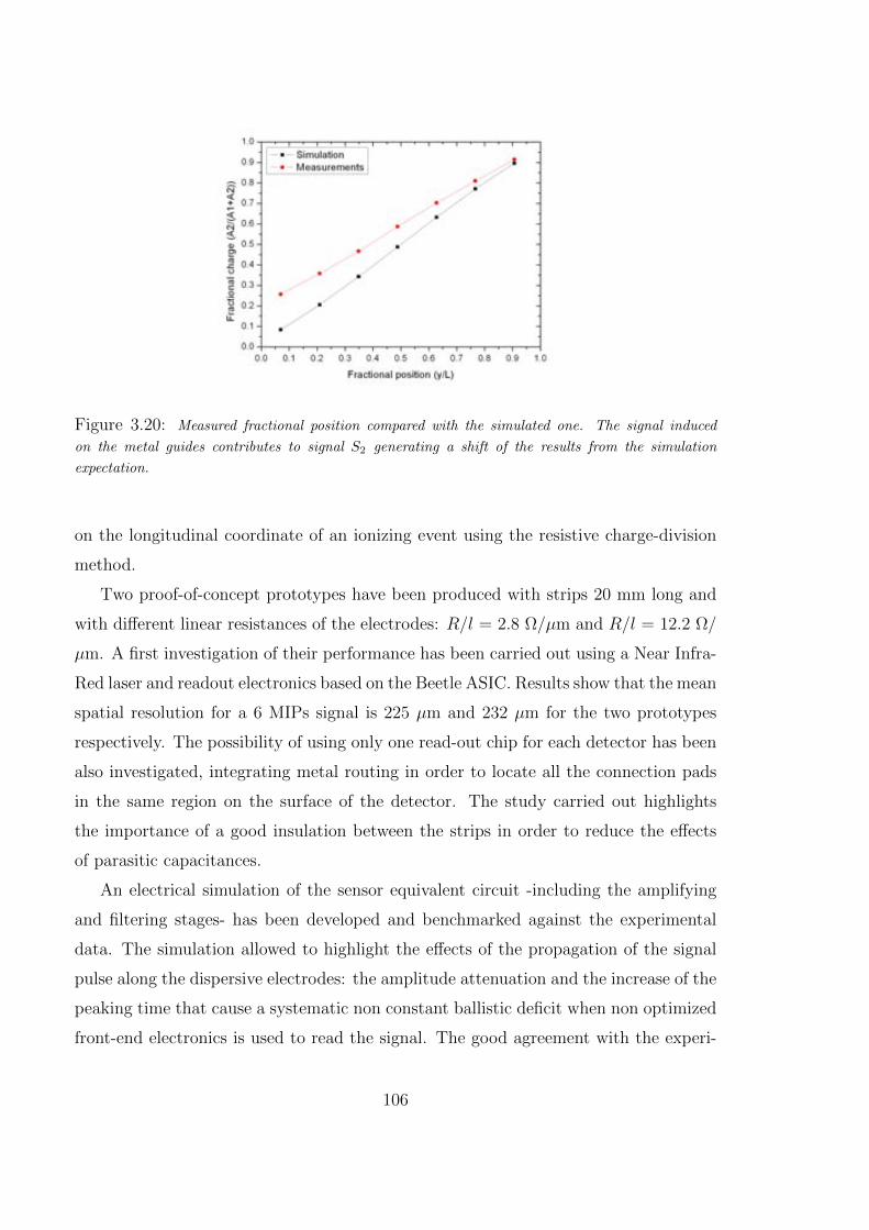
Figure 3.20: Measured fractional position compared with the simulated one. The signal induced
on the metal guides contributes to signal S2 generating a shift of the results from the simulation
expectation.
on the longitudinal coordinate of an ionizing event using the resistive charge-division
method.
Two proof-of-concept prototypes have been produced with strips 20 mm long and
with dierent linear resistances of the electrodes: R=l = 2:8 =m and R=l = 12.2 =
m. A rst investigation of their performance has been carried out using a Near Infra-
Red laser and readout electronics based on the Beetle ASIC. Results show that the mean
spatial resolution for a 6 MIPs signal is 225 m and 232 m for the two prototypes
respectively. The possibility of using only one read-out chip for each detector has been
also investigated, integrating metal routing in order to locate all the connection pads
in the same region on the surface of the detector. The study carried out highlights
the importance of a good insulation between the strips in order to reduce the eects
of parasitic capacitances.
An electrical simulation of the sensor equivalent circuit -including the amplifying
and ltering stages- has been developed and benchmarked against the experimental
data. The simulation allowed to highlight the eects of the propagation of the signal
pulse along the dispersive electrodes: the amplitude attenuation and the increase of the
peaking time that cause a systematic non constant ballistic decit when non optimized
front-end electronics is used to read the signal. The good agreement with the experi-
106

mental results in reconstructing the fractional position of the signal generation point
validates the electrical simulation as an adequate tool for future sensor optimization.
This initial study demonstrates the feasibility of the resistive charge division method
in a fully edged microstrip sensor with resistive electrodes. Specic studies on detec-
tion of minimum ionizing particles are in progress to assess its soundness as tracking
technology for the future particle physics experiments: the analysis of the data recorded
with a pion test beam at the CERN SPS beam line H6 is being carried out; neverthe-
less, in its current conception, this implementation appears as a suitable technology for
highly ionizing particles as it is the case of neutron monitors based on conversion lay-
ers or other nuclear imaging technologies ranging from Compton cameras to heavy-ion
detection.
In view of future prototypes fabrication it is worth to pay attention to the optimiza-
tion of the spatial resolution. As seen in section 3.3.3 it strongly depends on the signal
to noise ratio, that will be optimal when the shaper time constant is proportional to
the detector time constant. Considering the detector design, the detector time con-
stant should be kept small and the interstrip capacitance as small as possible, without
aecting the others characteristics of the device.
Using the simulation model described in section 3.2.2, relative values of the detector
and shaper time constants can be adjusted in order to eliminate the sistematic eect
of the ballistic decit. Then, depending on the experiment and the electronics used,
it is possible to replace the model of the ideal readout electronics with the one of the
real chip and denitely tune the parameters of interest to optimize the signal to noise
ratio.
107

108

Chapter 4
Stripixel detectors
In the previous chapters two single-sided detectors characterized by microstrip elec-
trodes have been introduced and studied. The attention has been mainly focused on the
possibility of obtaining specic capabilities, e.g. IR light transparency or 2D position-
sensing, by properly changing some parameters of their simple design and standard
technology.
Since 2003, other electrode geometries and technologies are being studied at the
Brookhaven National Laboratory of New York [74] in order to obtain a device that
could provide 2D position-sensitivity with a moderate number of readout electronic
channels and single-sided detector fabrication process. The concept is based on pixel
electrodes arranged in a projective X-U read-out conguration that allow to use a
minimum number of readout channels (2N) to process the information read from N2
pixels. Many designs and prototypes of so called stripixel detectors have been developed
over the years [75],[76], [77].
The rst generation consisted of planar p+-in-n pixel detectors, in which the n+
electrode was uniformly implanted from one side of the substrate, while the p+ elec-
trodes, on the other side, were divided into X- and Y-cells, and two metal layers were
used to readout the pixels by means of two sets of crossed strips on the detector sur-
face. An attempt to move and segment the n+ electrodes to the same side of the p+
failed due to diculties in generating the electric eld inside the substrate. Then, the
interest in radiation-hardness and true single-sided processing has led to a deeper in-
vestigation in 3D technology and new electrodes arrangements, both types on one side
of the bulk. New technologies have been proposed based on mixed planar/3D processes
109
( single-column) and full 3D (double-column) process.
3D detector technology, based on a deep reactive ion etching process, is at the
moment available in only three investigation centres around the world, among which,
the IMB-CNM of Barcelona. For this reason a collaboration between the BNL and the
IMB-CNM started in 2006 in order to carry out the full process of the new prototypes.
In this chapter, after a brief overview of the stripixel concept and the dierent
designs proposed over the years, the last prototypes, designed and totally fabricated in
the IMB-CNM clean room facilities, will be presented.
The new device is a dual-column 3D detector in which the p+ and n+ columns
are both processed on one side of the wafer and arranged in quincunx pattern (with
the p+ columns as the central elements). A net of perpendicular strips is dened
on the surface by means of two dierent metal layers to allow a projective X-Y read
out. 3D and 2D simulations have been performed in order to optimize the design of
the devices, then they have been fabricated. The processes ow, including a total
of 10 photolithography steps, has been the most challenging ever carried out at the
IMB-CNM for silicon detectors fabrication. After it, many samples and test structures
included in the wafer have been electrically characterized. The active area limitations
have been investigated with the use of Transient Current Technique measurements,
performed with dierent lasers of dierent wavelengths in the BNL instrumentation
division laboratory. Finally, two-dimensional position sensitivity has been tested using
a collimated laser set up and the ALIBAVA readout system in the IFCA clean room
facility in Santander. The development of the device supported by the simulation study
will be presented in the next sections as well as the experimental results.
This work has been carried out within the CERN RD50 collaboration, which has
the purpose of developing new high radiation hard detectors for future high luminosity
colliders (see section 1.4.1).
4.1 Stripixel detector concept: state of the art
In 2004 Z. Li presented the stripixel detector concept and the simulation, design
and fabrication of the rst prototypes fully carried out at the BNL [75]. The idea
was combining the advantages of a double-sided strip detector with the ones of a
110
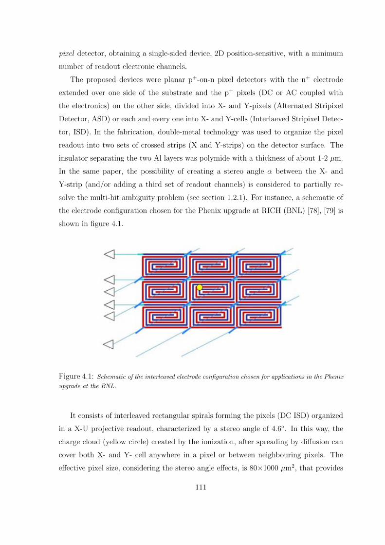
pixel detector, obtaining a single-sided device, 2D position-sensitive, with a minimum
number of readout electronic channels.
The proposed devices were planar p+-on-n pixel detectors with the n+ electrode
extended over one side of the substrate and the p+ pixels (DC or AC coupled with
the electronics) on the other side, divided into X- and Y-pixels (Alternated Stripixel
Detector, ASD) or each and every one into X- and Y-cells (Interlaeved Stripixel Detec-
tor, ISD). In the fabrication, double-metal technology was used to organize the pixel
readout into two sets of crossed strips (X and Y-strips) on the detector surface. The
insulator separating the two Al layers was polymide with a thickness of about 1-2 m.
In the same paper, the possibility of creating a stereo angle between the X- and
Y-strip (and/or adding a third set of readout channels) is considered to partially re-
solve the multi-hit ambiguity problem (see section 1.2.1). For instance, a schematic of
the electrode conguration chosen for the Phenix upgrade at RICH (BNL) [78], [79] is
shown in gure 4.1.
Figure 4.1: Schematic of the interleaved electrode conguration chosen for applications in the Phenix
upgrade at the BNL.
It consists of interleaved rectangular spirals forming the pixels (DC ISD) organized
in a X-U projective readout, characterized by a stereo angle of 4.6. In this way, the
charge cloud (yellow circle) created by the ionization, after spreading by diusion can
cover both X- and Y- cell anywhere in a pixel or between neighbouring pixels. The
eective pixel size, considering the stereo angle eects, is 801000 m2, that provides
111

a spatial resolution of 33.6 m for X-stripixel (35.2 m for U-stripixel) and a signal to
noise ratio of 10.4.
Then, in 2005 a collaboration with the IMB-CNM started with the purpose of
integrating in the stripixel concept a partial (single column) or a full (dual column) 3D
processing of the electrodes. The idea was to address this new investigation to these
applications that would demand high radiation hardness of the instrumentation.
As introduced in chapter 1.2.3, 3D detectors have the capability to withstand high
radiation uences. Thanks to the very short distance between electrodes, their deple-
tion voltage is substantially reduced with respect to planar detectors, and it should be
possible to fully deplete them after high radiation doses as well as reducing charge col-
lection degradation. These characteristics make 3D detectors suitable for applications
in experiments in future accelerators, characterized by a severe radiation environment
such as the case of LHC upgrade (HL-LHC).
Figure 4.2: Schematics of the stripixel electrode arrangement in the single column and dual-column
device. The top gure showsa detail of the detector layout, while the bottom gures show a section of
one cell (red line) is represented for the single column and the dual column case on the left and on the
right respectively.
The new 3D detectors were designed to have true single-sided process and both p+
and n+ electrodes on one side of the detector. The design of two dierent devices has
been developed: one with dual-column (p+ and n+) electrodes and another with single-
column and planar electrodes (p+ or n+). A comparison between one half of a single cell
112
of both the devices is shown in gure 4.2, under the schematics of the pixels layout.
A mask set was completed and used for a prototype run of single-column stripixel
detectors with x-pitch of 1000 m and y-pitch of 80 m. The n+ columns, 240 m
deep, have been etched by IMB-CNM of Barcelona on a batch of 300 m thick FZ p-
type Si wafers, then BNL nished the remaining planar processing involving phosphorus
implantations to connect the n+ columns of each pixel, p+ electrodes implantation and
two-metal layers deposition and isolation. Electrical simulation demonstrated that
detectors would be characterized by lower electric eld regions expecially under the p+
implants.
4.2 New prototype generation: a single side double
strip detector
In 2009 the development of dual-column 3D stripixel detector started. The generic
layout of the new device consists of p+ and n+ columns, both etched from one side of the
bulk and connected by means of two layers of metal strips crossed on the surface. The
main purpose of this project was to test the capability of the double-metal readout and
the complexity of the dual-column technology applied to the same surface. A simple
schematic of the device is shown in gure 4.3.
4.2.1 Optimization of the design: device simulation
The nal layout of the detector has been decided after a preliminary study of its
behaviour by means of computer simulations. The interest was focused on the electric
eld (electrostatic potential) distribution inside the silicon bulk, for dierent values of
Vbias and for dierent doping types (n or p) and electrodes (guard ring) congurations.
The aim was improving the guard ring isolation capability and reducing the eects of
the defects introduced by the saw cut at the edges of the device (see section 1.2.4),in
order to properly dene the active area of the sensor. For this purpose Synopsys TCAD
Sentaurus [80], a nite-element semiconductor simulation package, has been used.
In section 1.1 the basic dierential equations of semiconductor physics were intro-
duced. By solving these equations with appropriate boundary conditions, the behaviour
113
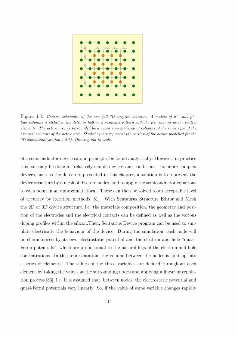
Figure 4.3: Generic schematic of the new full 3D stripixel detector. A matrix of n+- and p+-
type columns is etched in the detector bulk in a quincunx pattern with the p+ columns as the central
elements. The active area is surrounded by a guard ring made up of columns of the same type of the
external columns of the active area. Shaded square represent the portion of the device modelled for the
3D simulation( section 4.2.1). Drawing not to scale.
of a semiconductor device can, in principle, be found analytically. However, in practice
this can only be done for relatively simple devices and conditions. For more complex
devices, such as the detectors presented in this chapter, a solution is to represent the
device structure by a mesh of discrete nodes, and to apply the semiconductor equations
to each point in an approximate form. These can then be solved to an acceptable level
of accuracy by iteration methods [81]. With Sentaurus Structure Editor and Mesh
the 2D or 3D device structure, i.e. the materials composition, the geometry and posi-
tion of the electrodes and the electrical contacts can be dened as well as the various
doping proles within the silicon.Then, Sentaurus Device program can be used to sim-
ulate electrically the behaviour of the device. During the simulation, each node will
be characterised by its own electrostatic potential and the electron and hole \quasi-
Fermi potentials", which are proportional to the natural logs of the electron and hole
concentrations. In this representation, the volume between the nodes is split up into
a series of elements. The values of the three variables are dened throughout each
element by taking the values at the surrounding nodes and applying a linear interpola-
tion process [83], i.e. it is assumed that, between nodes, the electrostatic potential and
quasi-Fermi potentials vary linearly. So, if the value of some variable changes rapidly
114

across a region containing few nodes, the accuracy of the simulation will be reduced.
However, as the number of nodes increases (there is a limit for 2D and 3D models), the
resulting system of equations gets larger and the solving process becomes slower and
more dicult. To avoid these problems it is possible to use a high mesh density only in
the regions where the doping concentration changes rapidly or the electric eld is high.
For the same reason, considering the large size of semiconductor detectors with respect
to common micro- or nano-electronic devices (to which Synopsys TCAD is mainly ded-
icated), it is advisable to model as carefully as possible only a portion of the detector.
Actually, in general, a detector will have a repetitive structure, with many pixels or
strips, and in a steady state it will have a repetitive eld pattern, carrier densities
etc. At the contacts, the boundary conditions generally consist in a xed electrostatic
potential, and neutrality of charge. At the boundaries of the device mesh, the default
conditions are that the electric eld and current densities normal to the boundary are
zero. These are referred to as re ecting or Neumann boundary conditions and are also
applied to the external surface of dielectric layers such as SiO2. In a real detector in a
steady-state, these conditions will naturally occur along planes of symmetry inside the
device as well as along the external surfaces when the chip is \clean". This means that
basic steady-state simulations can be done using just the simplest repeating unit of the
detector. However, in order to investigate the electric eld distribution in the bulk of
the detector close to its edges, the simulations presented in this section involve a larger
region of the detector and 2D simulations have been performed of wider sections. In
gure 4.4 the two main structures considered in the 3D simulations are shown. In both
cases a corner (see gure 4.3) of the active area and of the guard ring of the sensor
is considered. The guard ring of the sensor has a squared shape made up of just one
line of columns of the same type of the external columns in the active area, in order to
x to zero the electric eld outside the active area. The distance between columns of
the same type is 80m, so the simulation mesh has a volume of 160m by 160m by
300m with more than 300000 nodes. The column type of the guard ring is the same
as the bulk and as the external columns of the active area (see gure 4.3). The specic
details of the simulated structures are as follows:
The substrate is 300 m thick, with constant 51011 cm3 phosphorus (a) or
11012 cm3 boron (b) doping.
115
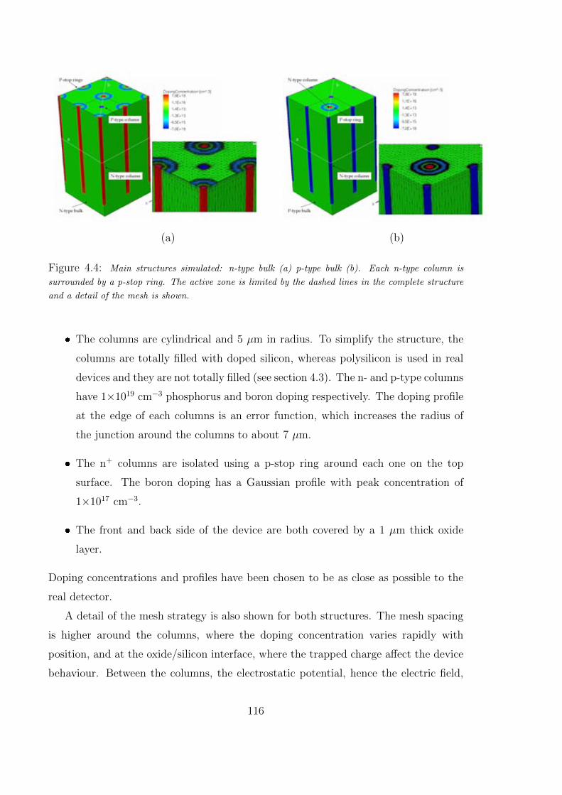
(a) (b)
Figure 4.4: Main structures simulated: n-type bulk (a) p-type bulk (b). Each n-type column is
surrounded by a p-stop ring. The active zone is limited by the dashed lines in the complete structure
and a detail of the mesh is shown.
The columns are cylindrical and 5 m in radius. To simplify the structure, the
columns are totally lled with doped silicon, whereas polysilicon is used in real
devices and they are not totally lled (see section 4.3). The n- and p-type columns
have 11019 cm3 phosphorus and boron doping respectively. The doping prole
at the edge of each columns is an error function, which increases the radius of
the junction around the columns to about 7 m.
The n+ columns are isolated using a p-stop ring around each one on the top
surface. The boron doping has a Gaussian prole with peak concentration of
11017 cm3.
The front and back side of the device are both covered by a 1 m thick oxide
layer.
Doping concentrations and proles have been chosen to be as close as possible to the
real detector.
A detail of the mesh strategy is also shown for both structures. The mesh spacing
is higher around the columns, where the doping concentration varies rapidly with
position, and at the oxide/silicon interface, where the trapped charge aect the device
behaviour. Between the columns, the electrostatic potential, hence the electric eld,
116
varies rapidly with the horizontal coordinate, but not along the z-direction. As a
consequence, the vertical mesh spacing is wider.
After creating the mesh, the Sentaurus Device program has been used inside the
Workbench framework to run the simulations. The physics models needed in the
simulation can be specify in the text le that control the program, as well as the
conditions that one want to simulate. Starting from the basic semiconductor physics
equations, Synopsys accepts many dierent and more complicated models in order
to correctly handle with the full device as well as with specic regions or conditions
inside its volume. In the simulations presented in this section, the mobility of the
carriers was taken into account using doping-concentration-dependent and high-eld-
saturation-dependent physical models. This means that the electron and hole velocities
cannot increase without limit as the electric eld gets stronger, but will instead reach
a saturation velocity. Then, the carrier generation and recombination rates are based
on a Shockley-Read-Hall model and depend on the electron and hole concentrations
and the doping density.
In order to account for the state charge induced at the interface between the silicon
substrate and the oxide layer discussed in sections 1.2.4 2.4.1, a xed positive charge
of 21010 cm2 has been introduced. Specic information on all the models and con-
ditions available in Sentaurus Device can be found in the dedicated user's guide [82].
Using all the proper models for our structures a quasi-stationary simulation was
run, where the bias applied to the detector was steadily increased from 0V to 15V in
consecutive steps, to nd how the depletion region and electric eld pattern develop.
At each step, the time-dependent terms in the semiconductor equations are zero and
an initial guess at the correct solution is found by extrapolation from the previous
solutions; then a global approximate Newton method is used to solve the equations
system to an acceptable level of accuracy.
In both structures, the depletion region start from the p+-type columns and grows
cylindrically outwards. The distance between a p-type and a n-type column is 56.6 m.
So, the lateral depletion, i.e. the depletion of the zone between columns of opposite
doping, occurs at low voltage, around 4V for both types of bulk. Figure 4.5 shows
the electric eld strength and voltage distribution in an horizontal cross section (white
section (a) in gure 4.5) of both structures in correspondence of the half of the columns
117
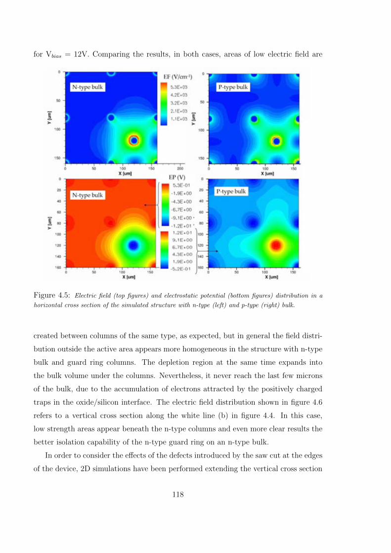
for Vbias = 12V. Comparing the results, in both cases, areas of low electric eld are
Figure 4.5: Electric eld (top gures) and electrostatic potential (bottom gures) distribution in a
horizontal cross section of the simulated structure with n-type (left) and p-type (right) bulk.
created between columns of the same type, as expected, but in general the eld distri-
bution outside the active area appears more homogeneous in the structure with n-type
bulk and guard ring columns. The depletion region at the same time expands into
the bulk volume under the columns. Nevertheless, it never reach the last few microns
of the bulk, due to the accumulation of electrons attracted by the positively charged
traps in the oxide/silicon interface. The electric eld distribution shown in gure 4.6
refers to a vertical cross section along the white line (b) in gure 4.4. In this case,
low strength areas appear beneath the n-type columns and even more clear results the
better isolation capability of the n-type guard ring on an n-type bulk.
In order to consider the eects of the defects introduced by the saw cut at the edges
of the device, 2D simulations have been performed extending the vertical cross section
118

Figure 4.6: Electric eld distribution in a vertical cross section of the simulated structure with n-type
(left) and p-type (right) bulk.
of both models to the edge, 100 m (p
2 in the cross section) far from the guard
ring, and to two more columns inside the active region. The defects along the edge
have been simulated using the model presented in reference [84]. It consists in lling
consecutive regions (in our case 4 regions 4.5 m wide) with dierent concentration of
neutral carrier traps (both electrons and holes) with an exponential energy distribution
close to the conductive band. Concentration of each trap type decreases from the bare
edge inwards. Figure 4.7 shows the results of the simulations concerning the electric
eld distribution for Vbias=12V. Again, the n-type bulk and guard ring result to be
more eective in dening and isolating the active area of the detector. Following the
hints of these results the n-type bulk conguration has been chosen for the prototypes
production.
4.2.2 Layout of the detectors
A mask set has been designed for the production of baby sensors and test structures.
Each device has a surface of 11 cm2 area in which the columns electrodes are
arranged in a diamond pattern. The n+ columns are surrounded each one by a p-stop
ring in order to avoid any short circuit through the charges in the silicon/oxide interface
between electrodes of dierent strips (see section 1.2.4). Then, two sets of perpendicular
119

Figure 4.7: 2D simulation Electric eld distribution in a vertical cross section of the simulated
structure with n-type (left) and p-type (right) bulk.
metal strips, 127 X-strips (p-type columns) and 128 Y-strips (n-type columns) with a
X-pitch = Y-pitch of 80 m, 10 m wide and separated by a dielectric layer are dened
on the surface directly contacting with the electrodes (Schottky contacts) to allow a
projective X-Y read out (see gure 4.3). The active area is surrounded by a guard
ring made up of n+ columns with the same pitch and distance as the others connected
by the Y-strips. Other detector models have been considered in the mask design in
order to extract information by comparing the results of their characterization. Some
devices with X- and Y-pitch of 160 m have been added as well as some else with
pitch of 80 m but with polysilicon connections between p+ columns instead of metal1.
Detectors with 80 m or 160 m pitch and readout pads inside the guard ring perimeter
have been included in order to investigate the possibility of obtaining detectors with a
reduced dead area around the active area.
The mask is then completed by dierent 1D position-sensitive or diode test struc-
tures obtained by shorting the n-type and/or the p-type pads in order to simplify the
connection with the electronics chains for dierent characterization measurements. All
1The design of these detectors has been developed at the same time of the design of the detectors
presented in the previous chapter. The interest in polysilicon as contact material has been extended
to these devices too.
120
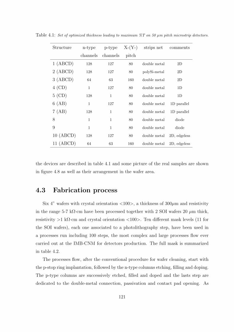
Table 4.1: Set of optimized thickness leading to maximum %T on 50 m pitch microstrip detectors.
Structure n-type p-type X-(Y-) strips net comments
channels channels pitch
1 (ABCD) 128 127 80 double metal 2D
2 (ABCD) 128 127 80 polySi-metal 2D
3 (ABCD) 64 63 160 double metal 2D
4 (CD) 1 127 80 double metal 1D
5 (CD) 128 1 80 double metal 1D
6 (AB) 1 127 80 double metal 1D parallel
7 (AB) 128 1 80 double metal 1D parallel
8 1 1 80 double metal diode
9 1 1 80 double metal diode
10 (ABCD) 128 127 80 double metal 2D, edgeless
11 (ABCD) 64 63 160 double metal 2D, edgeless
the devices are described in table 4.1 and some picture of the real samples are shown
in gure 4.8 as well as their arrangement in the wafer area.
4.3 Fabrication process
Six 4" wafers with crystal orientation <100>, a thickness of 300m and resistivity
in the range 5-7 kcm have been processed together with 2 SOI wafers 20 m thick,
resistivity >1 kcm and crystal orientation <100>. Ten dierent mask levels (11 for
the SOI wafers), each one associated to a photolithography step, have been used in
a processes run including 100 steps, the most complex and large processes ow ever
carried out at the IMB-CNM for detectors production. The full mask is summarized
in table 4.2.
The processes ow, after the conventional procedure for wafer cleaning, start with
the p-stop ring implantation, followed by the n-type columns etching, lling and doping.
The p-type columns are successively etched, lled and doped and the lasts step are
dedicated to the double-metal connection, passivation and contact pad opening. As
121
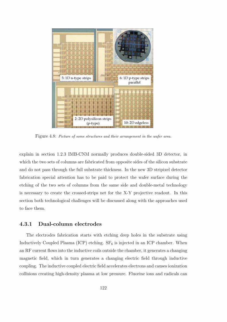
Figure 4.8: Picture of some structures and their arrangement in the wafer area.
explain in section 1.2.3 IMB-CNM normally produces double-sided 3D detector, in
which the two sets of columns are fabricated from opposite sides of the silicon substrate
and do not pass through the full substrate thickness. In the new 3D stripixel detector
fabrication special attention has to be paid to protect the wafer surface during the
etching of the two sets of columns from the same side and double-metal technology
is necessary to create the crossed-strips net for the X-Y projective readout. In this
section both technological challenges will be discussed along with the approaches used
to face them.
4.3.1 Dual-column electrodes
The electrodes fabrication starts with etching deep holes in the substrate using
Inductively Coupled Plasma (ICP) etching. SF6 is injected in an ICP chamber. When
an RF current ows into the inductive coils outside the chamber, it generates a changing
magnetic eld, which in turn generates a changing electric eld through inductive
coupling. The inductive coupled electric eld accelerates electrons and causes ionization
collisions creating high-density plasma at low pressure. Fluorine ions and radicals can
122

Table 4.2: Mask levels for the stripixel fabrication run carried out at the IMB-CNM clean room
facilities.
Level Pattern Comments
P-DIFF p-stop p-stop rings definition around n-type columns
N-HOLES n+ columns n+ columns etching
POLY polysilicon definition of the n+ columns on the surface
P-HOLES p+ columns p+ columns etching
POLY2 polysilicon definition of the p+ columns on the surface
WINDOW metal window removing SiO2 on the guard ring columns
and p-type columns to contact with the metal layer
METAL metal (first layer) first metal layer pattern definition
VIA metal2 window opening connection between two metal layers
and removing SiO2 on the p-type columns
METAL2 metal (second layer) second metal layer pattern definition
PASSIV metal contacts opening windows on the metal connection pads
BACK WINDOW SOI wafer etching the support substrate up to SOI wafers
then be accelerated onto the wafer surface, where they react quickly with silicon and
etch it; the etch product is SiF4. One of the most important advantages of ICP system
is that the ion bombardment ux and ion bombardment energy can be independently
controlled by the source power and bias RF power, respectively. Then, low pressure of
the system translates into longer ions main free path and less ion collision scattering,
that enhances etch prole control. Nevertheless, going on etching the columns through
the mask pattern (levels N-HOLES and P-HOLES in table 4.2), unreacted uorine will
accumulate and etch away the sides of the holes. To avoid this, periodically during
the process the SF6 is pumped out of the chamber and C4F8 is injected and ionized
to create a polymer chain of CF2 which is deposited on the substrate. This polymer
protects the sides of the holes from chemical etching during the next etching step.
The sequence of steps go on up to the desired depth of the column; endpoint of the
process is determined by time, which has been previously calibrated. Ideally, the holes
123
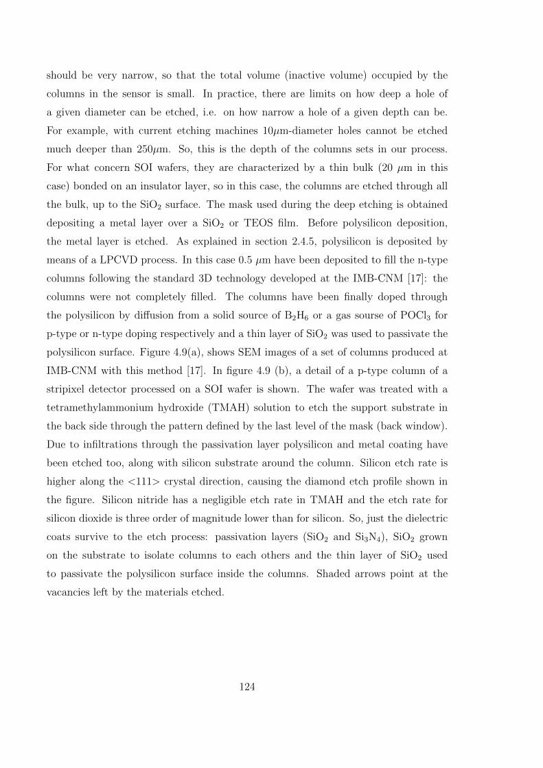
should be very narrow, so that the total volume (inactive volume) occupied by the
columns in the sensor is small. In practice, there are limits on how deep a hole of
a given diameter can be etched, i.e. on how narrow a hole of a given depth can be.
For example, with current etching machines 10m-diameter holes cannot be etched
much deeper than 250m. So, this is the depth of the columns sets in our process.
For what concern SOI wafers, they are characterized by a thin bulk (20 m in this
case) bonded on an insulator layer, so in this case, the columns are etched through all
the bulk, up to the SiO2 surface. The mask used during the deep etching is obtained
depositing a metal layer over a SiO2 or TEOS lm. Before polysilicon deposition,
the metal layer is etched. As explained in section 2.4.5, polysilicon is deposited by
means of a LPCVD process. In this case 0.5 m have been deposited to ll the n-type
columns following the standard 3D technology developed at the IMB-CNM [17]: the
columns were not completely lled. The columns have been nally doped through
the polysilicon by diusion from a solid source of B2H6 or a gas sourse of POCl3 for
p-type or n-type doping respectively and a thin layer of SiO2 was used to passivate the
polysilicon surface. Figure 4.9(a), shows SEM images of a set of columns produced at
IMB-CNM with this method [17]. In gure 4.9 (b), a detail of a p-type column of a
stripixel detector processed on a SOI wafer is shown. The wafer was treated with a
tetramethylammonium hydroxide (TMAH) solution to etch the support substrate in
the back side through the pattern dened by the last level of the mask (back window).
Due to inltrations through the passivation layer polysilicon and metal coating have
been etched too, along with silicon substrate around the column. Silicon etch rate is
higher along the <111> crystal direction, causing the diamond etch prole shown in
the gure. Silicon nitride has a negligible etch rate in TMAH and the etch rate for
silicon dioxide is three order of magnitude lower than for silicon. So, just the dielectric
coats survive to the etch process: passivation layers (SiO2 and Si3N4), SiO2 grown
on the substrate to isolate columns to each others and the thin layer of SiO2 used
to passivate the polysilicon surface inside the columns. Shaded arrows point at the
vacancies left by the materials etched.
124
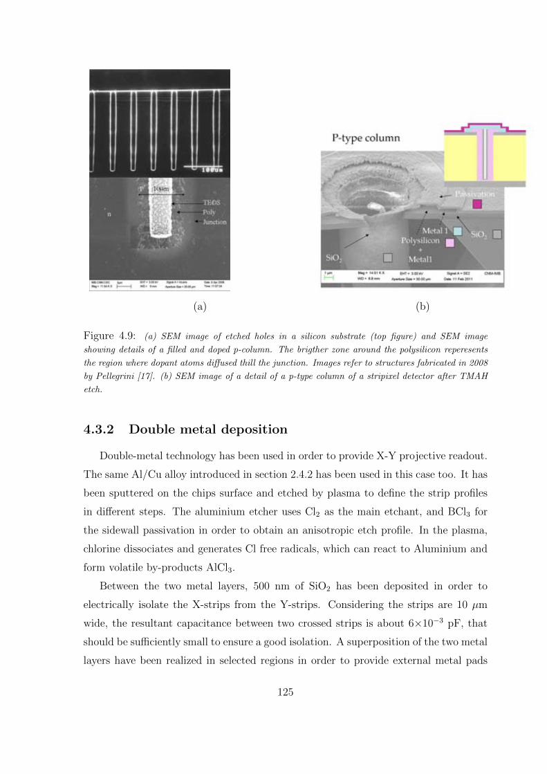
(a) (b)
Figure 4.9: (a) SEM image of etched holes in a silicon substrate (top gure) and SEM image
showing details of a lled and doped p-column. The brigther zone around the polysilicon reperesents
the region where dopant atoms diused thill the junction. Images refer to structures fabricated in 2008
by Pellegrini [17]. (b) SEM image of a detail of a p-type column of a stripixel detector after TMAH
etch.
4.3.2 Double metal deposition
Double-metal technology has been used in order to provide X-Y projective readout.
The same Al/Cu alloy introduced in section 2.4.2 has been used in this case too. It has
been sputtered on the chips surface and etched by plasma to dene the strip proles
in dierent steps. The aluminium etcher uses Cl2 as the main etchant, and BCl3 for
the sidewall passivation in order to obtain an anisotropic etch prole. In the plasma,
chlorine dissociates and generates Cl free radicals, which can react to Aluminium and
form volatile by-products AlCl3.
Between the two metal layers, 500 nm of SiO2 has been deposited in order to
electrically isolate the X-strips from the Y-strips. Considering the strips are 10 m
wide, the resultant capacitance between two crossed strips is about 6103 pF, that
should be suciently small to ensure a good isolation. A superposition of the two metal
layers have been realized in selected regions in order to provide external metal pads
125
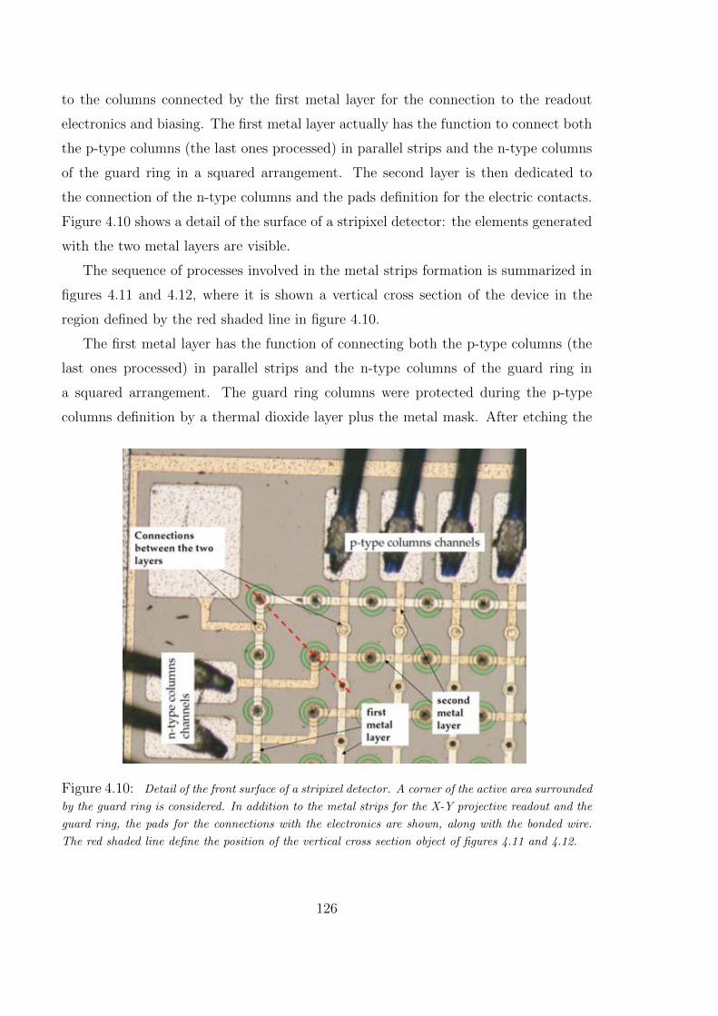
to the columns connected by the rst metal layer for the connection to the readout
electronics and biasing. The rst metal layer actually has the function to connect both
the p-type columns (the last ones processed) in parallel strips and the n-type columns
of the guard ring in a squared arrangement. The second layer is then dedicated to
the connection of the n-type columns and the pads denition for the electric contacts.
Figure 4.10 shows a detail of the surface of a stripixel detector: the elements generated
with the two metal layers are visible.
The sequence of processes involved in the metal strips formation is summarized in
gures 4.11 and 4.12, where it is shown a vertical cross section of the device in the
region dened by the red shaded line in gure 4.10.
The rst metal layer has the function of connecting both the p-type columns (the
last ones processed) in parallel strips and the n-type columns of the guard ring in
a squared arrangement. The guard ring columns were protected during the p-type
columns denition by a thermal dioxide layer plus the metal mask. After etching the
Figure 4.10: Detail of the front surface of a stripixel detector. A corner of the active area surrounded
by the guard ring is considered. In addition to the metal strips for the X-Y projective readout and the
guard ring, the pads for the connections with the electronics are shown, along with the bonded wire.
The red shaded line dene the position of the vertical cross section object of gures 4.11 and 4.12.
126
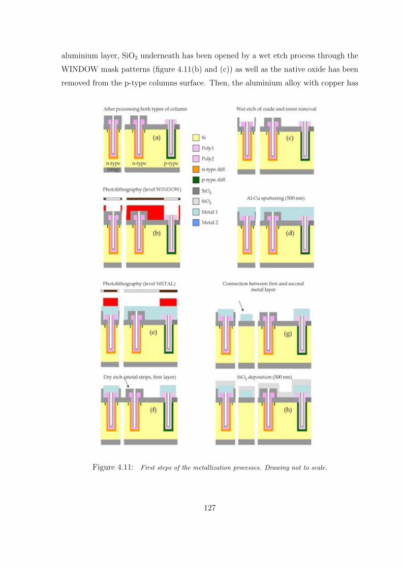
aluminium layer, SiO2 underneath has been opened by a wet etch process through the
WINDOW mask patterns (gure 4.11(b) and (c)) as well as the native oxide has been
removed from the p-type columns surface. Then, the aluminium alloy with copper has
Figure 4.11: First steps of the metallization processes. Drawing not to scale.
127
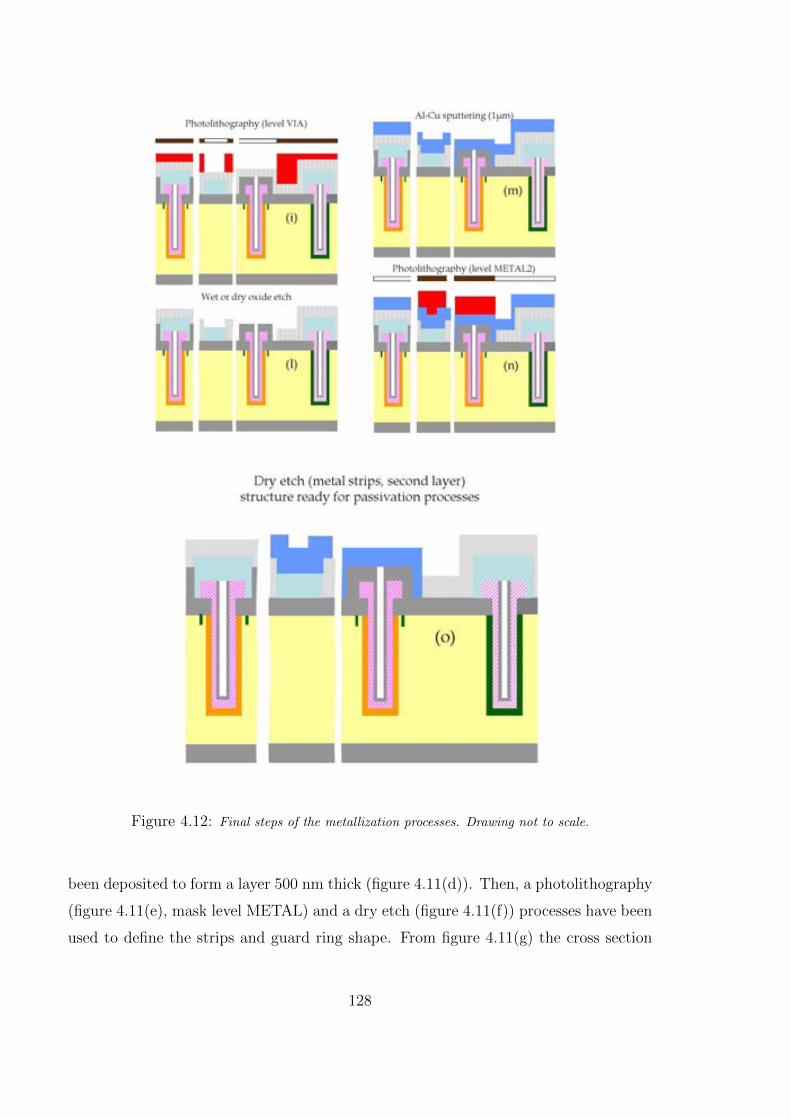
Figure 4.12: Final steps of the metallization processes. Drawing not to scale.
been deposited to form a layer 500 nm thick (gure 4.11(d)). Then, a photolithography
(gure 4.11(e), mask level METAL) and a dry etch (gure 4.11(f)) processes have been
used to dene the strips and guard ring shape. From gure 4.11(g) the cross section
128
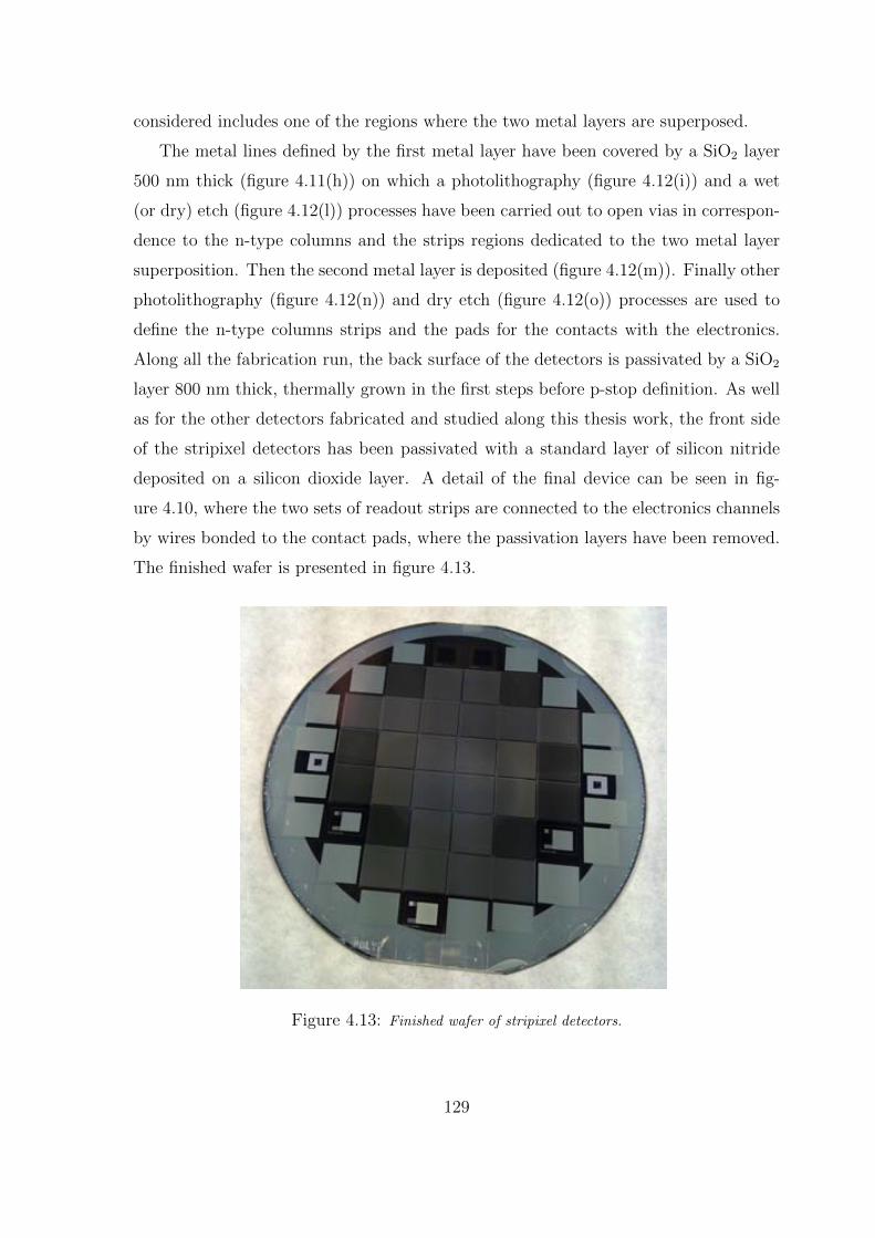
considered includes one of the regions where the two metal layers are superposed.
The metal lines dened by the rst metal layer have been covered by a SiO2 layer
500 nm thick (gure 4.11(h)) on which a photolithography (gure 4.12(i)) and a wet
(or dry) etch (gure 4.12(l)) processes have been carried out to open vias in correspon-
dence to the n-type columns and the strips regions dedicated to the two metal layer
superposition. Then the second metal layer is deposited (gure 4.12(m)). Finally other
photolithography (gure 4.12(n)) and dry etch (gure 4.12(o)) processes are used to
dene the n-type columns strips and the pads for the contacts with the electronics.
Along all the fabrication run, the back surface of the detectors is passivated by a SiO2
layer 800 nm thick, thermally grown in the rst steps before p-stop denition. As well
as for the other detectors fabricated and studied along this thesis work, the front side
of the stripixel detectors has been passivated with a standard layer of silicon nitride
deposited on a silicon dioxide layer. A detail of the nal device can be seen in g-
ure 4.10, where the two sets of readout strips are connected to the electronics channels
by wires bonded to the contact pads, where the passivation layers have been removed.
The nished wafer is presented in gure 4.13.
Figure 4.13: Finished wafer of stripixel detectors.
129
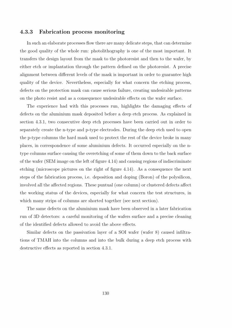
4.3.3 Fabrication process monitoring
In such an elaborate processes ow there are many delicate steps, that can determine
the good quality of the whole run: photolithography is one of the most important. It
transfers the design layout from the mask to the photoresist and then to the wafer, by
either etch or implantation through the pattern dened on the photoresist. A precise
alignment between dierent levels of the mask is important in order to guarantee high
quality of the device. Nevertheless, especially for what concern the etching process,
defects on the protection mask can cause serious failure, creating undesirable patterns
on the photo resist and as a consequence undesirable eects on the wafer surface.
The experience had with this processes run, highlights the damaging eects of
defects on the aluminium mask deposited before a deep etch process. As explained in
section 4.3.1, two consecutive deep etch processes have been carried out in order to
separately create the n-type and p-type electrodes. During the deep etch used to open
the p-type columns the hard mask used to protect the rest of the device broke in many
places, in correspondence of some aluminium defects. It occurred especially on the n-
type columns surface causing the overetching of some of them down to the back surface
of the wafer (SEM image on the left of gure 4.14) and causing regions of indiscriminate
etching (microscope pictures on the right of gure 4.14). As a consequence the next
steps of the fabrication process, i.e. deposition and doping (Boron) of the polysilicon,
involved all the aected regions. These puntual (one column) or clustered defects aect
the working status of the devices, especially for what concern the test structures, in
which many strips of columns are shorted together (see next section).
The same defects on the aluminium mask have been observed in a later fabrication
run of 3D detectors: a careful monitoring of the wafers surface and a precise cleaning
of the identied defects allowed to avoid the above eects.
Similar defects on the passivation layer of a SOI wafer (wafer 8) caused inltra-
tions of TMAH into the columns and into the bulk during a deep etch process with
destructive eects as reported in section 4.3.1.
130
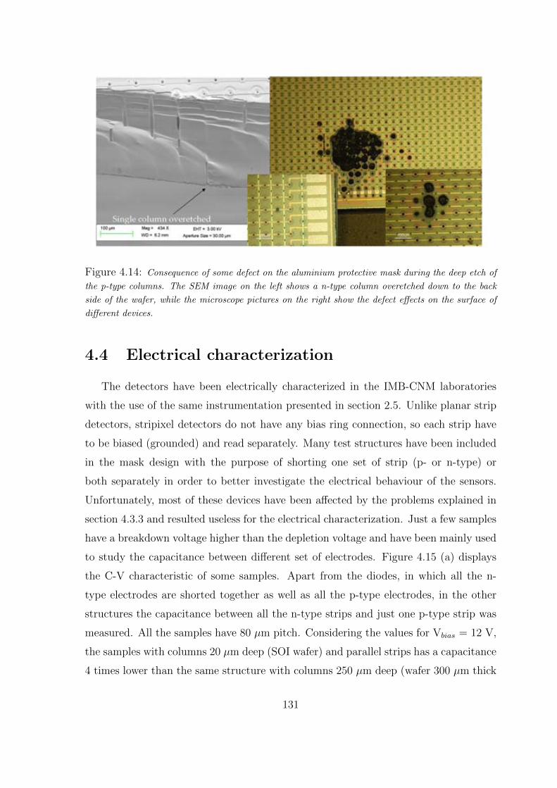
Figure 4.14: Consequence of some defect on the aluminium protective mask during the deep etch of
the p-type columns. The SEM image on the left shows a n-type column overetched down to the back
side of the wafer, while the microscope pictures on the right show the defect effects on the surface of
different devices.
4.4 Electrical characterization
The detectors have been electrically characterized in the IMB-CNM laboratories
with the use of the same instrumentation presented in section 2.5. Unlike planar strip
detectors, stripixel detectors do not have any bias ring connection, so each strip have
to be biased (grounded) and read separately. Many test structures have been included
in the mask design with the purpose of shorting one set of strip (p- or n-type) or
both separately in order to better investigate the electrical behaviour of the sensors.
Unfortunately, most of these devices have been affected by the problems explained in
section 4.3.3 and resulted useless for the electrical characterization. Just a few samples
have a breakdown voltage higher than the depletion voltage and have been mainly used
to study the capacitance between different set of electrodes. Figure 4.15 (a) displays
the C-V characteristic of some samples. Apart from the diodes, in which all the n-
type electrodes are shorted together as well as all the p-type electrodes, in the other
structures the capacitance between all the n-type strips and just one p-type strip was
measured. All the samples have 80 µ m pitch. Considering the values for Vbias = 12 V,
the samples with columns 20 µ m deep (SOI wafer) and parallel strips has a capacitance
4 times lower than the same structure with columns 250 µ m deep (wafer 300 µ m thick
131

(a) (b)
Figure 4.15: (a) C-V characteristic of dierent structures. See text for details. (b) 1/C2 dependence
to the bias voltage for two diodes, one from each type of wafer. The wafers have dierent resistivity.
and parallel strips), but only 2 times lower than the structures from the same wafer
and crossed strips. The values are in the range between 2 and 8 pF. The values of the
interstrip capacitance, i.e. the capacitance between one p-type strip and both its rst
neighbour strips have been measured on the same samples. The result obtained for the
detectors from the wafer SOI is independent of the parallel or crossed conguration of
the strips and takes a value of about 0.15 pF for Vbias = 12 V. The interstrip capacitance
of the sample with the columns 250 m deep, is 0.8 pF at the same voltage value.
The diode from the wafer SOI has a bulk capacitance of about 0.3 nF, while the
diode from the wafer 300 m thick of 1.2 nF. Figure 4.15 (b) shows the classic 1/C2
dependence to the bias voltage for both diodes. It can be noticed that the depletion
voltage of the detector from the wafer 300 m thick and resistivity in the range 5-
7 kcm is 3V < Vdepl < 4V as expected from the simulation results, while the
depletion voltage of the diode from the SOI wafer 20 m thick and resistivity >1 kcm,
is 5V < Vdepl < 6V. In both cases the distance between electrodes with dierent doping
is d = pitchp
2 56.6 m.
The results of the I-V characteristic measurements are shown in gures 4.16 (a) for
detectors 300 m thick and (b) for detectors 20 m thick. A current of about 10 nA has
been recorded from the detectors with columns 250 m deep, when just one p-type strip
132
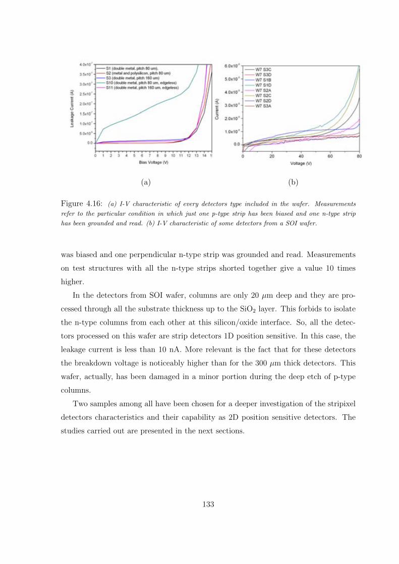
(a) (b)
Figure 4.16: (a) I-V characteristic of every detectors type included in the wafer. Measurements
refer to the particular condition in which just one p-type strip has been biased and one n-type strip
has been grounded and read. (b) I-V characteristic of some detectors from a SOI wafer.
was biased and one perpendicular n-type strip was grounded and read. Measurements
on test structures with all the n-type strips shorted together give a value 10 times
higher.
In the detectors from SOI wafer, columns are only 20 m deep and they are pro-
cessed through all the substrate thickness up to the SiO2 layer. This forbids to isolate
the n-type columns from each other at this silicon/oxide interface. So, all the detec-
tors processed on this wafer are strip detectors 1D position sensitive. In this case, the
leakage current is less than 10 nA. More relevant is the fact that for these detectors
the breakdown voltage is noticeably higher than for the 300 m thick detectors. This
wafer, actually, has been damaged in a minor portion during the deep etch of p-type
columns.
Two samples among all have been chosen for a deeper investigation of the stripixel
detectors characteristics and their capability as 2D position sensitive detectors. The
studies carried out are presented in the next sections.
133
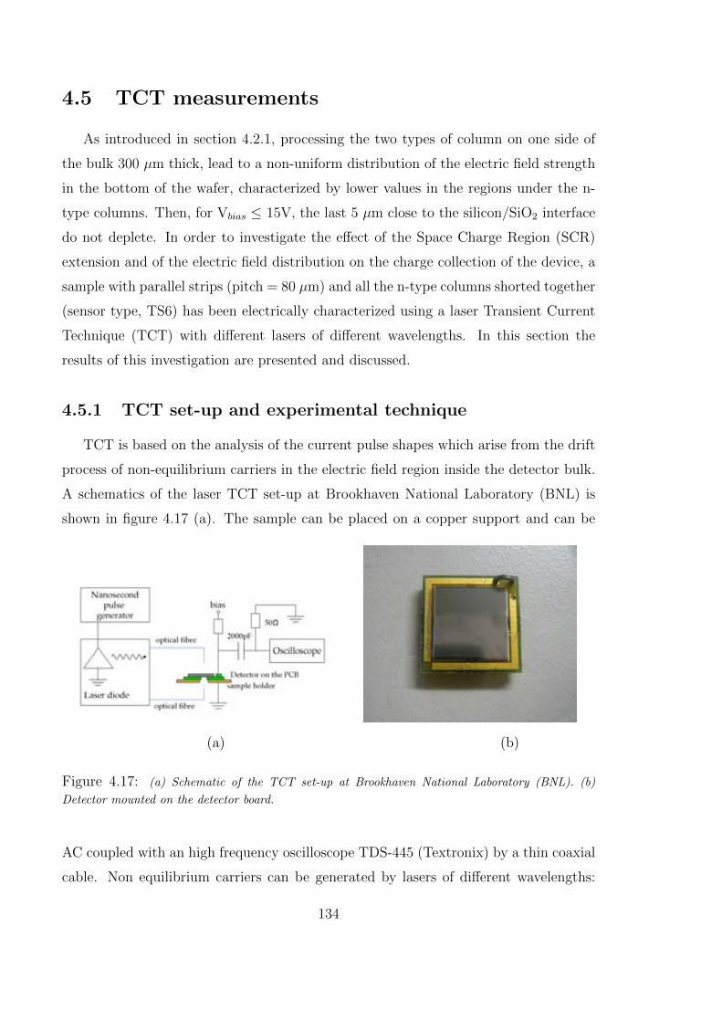
4.5 TCT measurements
As introduced in section 4.2.1, processing the two types of column on one side of
the bulk 300 m thick, lead to a non-uniform distribution of the electric eld strength
in the bottom of the wafer, characterized by lower values in the regions under the n-
type columns. Then, for Vbias 15V, the last 5 m close to the silicon/SiO2 interface
do not deplete. In order to investigate the eect of the Space Charge Region (SCR)
extension and of the electric eld distribution on the charge collection of the device, a
sample with parallel strips (pitch = 80 m) and all the n-type columns shorted together
(sensor type, TS6) has been electrically characterized using a laser Transient Current
Technique (TCT) with dierent lasers of dierent wavelengths. In this section the
results of this investigation are presented and discussed.
4.5.1 TCT set-up and experimental technique
TCT is based on the analysis of the current pulse shapes which arise from the drift
process of non-equilibrium carriers in the electric eld region inside the detector bulk.
A schematics of the laser TCT set-up at Brookhaven National Laboratory (BNL) is
shown in gure 4.17 (a). The sample can be placed on a copper support and can be
(a) (b)
Figure 4.17: (a) Schematic of the TCT set-up at Brookhaven National Laboratory (BNL). (b)
Detector mounted on the detector board.
AC coupled with an high frequency oscilloscope TDS-445 (Textronix) by a thin coaxial
cable. Non equilibrium carriers can be generated by lasers of dierent wavelengths:
134
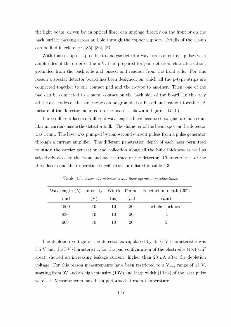
the light beam, driven by an optical bre, can impinge directly on the front or on the
back surface passing across an hole through the copper support. Details of the set-up
can be nd in references [85], [86], [87].
With this set-up it is possible to analyse detector waveforms of current pulses with
amplitudes of the order of the mV. It is prepared for pad detectors characterization,
grounded from the back side and biased and readout from the front side. For this
reason a special detector board has been designed, on which all the p-type strips are
connected together to one contact pad and the n-type to another. Then, one of the
pad can be connected to a metal contact on the back side of the board. In this way
all the electrodes of the same type can be grounded or biased and readout together. A
picture of the detector mounted on the board is shown in gure 4.17 (b).
Three dierent lasers of dierent wavelengths have been used to generate non equi-
librium carriers inside the detector bulk. The diameter of the beam spot on the detector
was 1 mm. The laser was pumped by nanosecond current pulses from a pulse generator
through a current amplier. The dierent penetration depth of each laser permitted
to study the carrier generation and collection along all the bulk thickness as well as
selectively close to the front and back surface of the detector. Characteristics of the
three lasers and their operation specications are listed in table 4.3.
Table 4.3: Laser characteristics and their operation specications.
Wavelength () Intensity Width Period Penetartion depth (20)
(nm) (V) (ns) (s) (m)
1060 10 10 20 whole thickness
830 10 10 20 15
660 10 10 20 5
The depletion voltage of the detector extrapolated by its C-V characteristic was
3.5 V and the I-V characteristic, for the pad conguration of the electrodes (11 cm2
area), showed an increasing leakage current, higher than 20 A after the depletion
voltage. For this reason measurements have been restricted to a Vbias range of 15 V,
starting from 0V and an high intensity (10V) and large width (10 ns) of the laser pulse
were set. Measurements have been performed at room temperature.
135
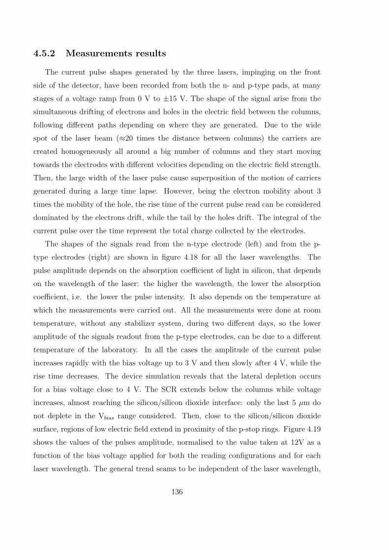
4.5.2 Measurements results
The current pulse shapes generated by the three lasers, impinging on the front
side of the detector, have been recorded from both the n- and p-type pads, at many
stages of a voltage ramp from 0 V to 15 V. The shape of the signal arise from the
simultaneous drifting of electrons and holes in the electric eld between the columns,
following dierent paths depending on where they are generated. Due to the wide
spot of the laser beam (20 times the distance between columns) the carriers are
created homogeneously all around a big number of columns and they start moving
towards the electrodes with dierent velocities depending on the electric eld strength.
Then, the large width of the laser pulse cause superposition of the motion of carriers
generated during a large time lapse. However, being the electron mobility about 3
times the mobility of the hole, the rise time of the current pulse read can be considered
dominated by the electrons drift, while the tail by the holes drift. The integral of the
current pulse over the time represent the total charge collected by the electrodes.
The shapes of the signals read from the n-type electrode (left) and from the p-
type electrodes (right) are shown in gure 4.18 for all the laser wavelengths. The
pulse amplitude depends on the absorption coecient of light in silicon, that depends
on the wavelength of the laser: the higher the wavelength, the lower the absorption
coecient, i.e. the lower the pulse intensity. It also depends on the temperature at
which the measurements were carried out. All the measurements were done at room
temperature, without any stabilizer system, during two dierent days, so the lower
amplitude of the signals readout from the p-type electrodes, can be due to a dierent
temperature of the laboratory. In all the cases the amplitude of the current pulse
increases rapidly with the bias voltage up to 3 V and then slowly after 4 V, while the
rise time decreases. The device simulation reveals that the lateral depletion occurs
for a bias voltage close to 4 V. The SCR extends below the columns while voltage
increases, almost reaching the silicon/silicon dioxide interface: only the last 5 m do
not deplete in the Vbias range considered. Then, close to the silicon/silicon dioxide
surface, regions of low electric eld extend in proximity of the p-stop rings. Figure 4.19
shows the values of the pulses amplitude, normalised to the value taken at 12V as a
function of the bias voltage applied for both the reading congurations and for each
laser wavelength. The general trend seams to be independent of the laser wavelength,
136
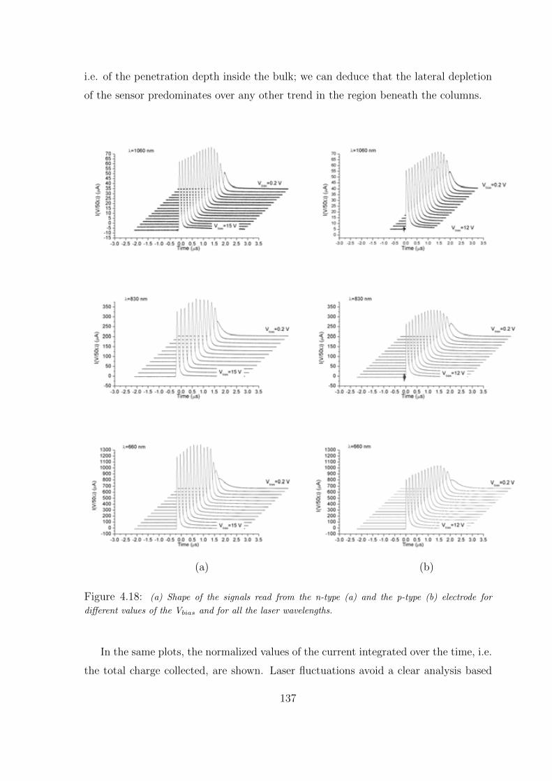
i.e. of the penetration depth inside the bulk; we can deduce that the lateral depletion
of the sensor predominates over any other trend in the region beneath the columns.
(a) (b)
Figure 4.18: (a) Shape of the signals read from the n-type (a) and the p-type (b) electrode for
dierent values of the Vbias and for all the laser wavelengths.
In the same plots, the normalized values of the current integrated over the time, i.e.
the total charge collected, are shown. Laser uctuations avoid a clear analysis based
137
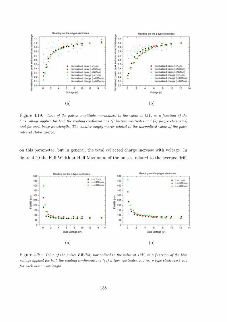
(a) (b)
Figure 4.19: Value of the pulses amplitude, normalised to the value at 12V, as a function of the
bias voltage applied for both the reading congurations ((a)n-type electrodes and (b) p-type electrodes)
and for each laser wavelength. The smaller empty marks related to the normalized value of the pulse
integral (total charge)
on this parameter, but in general, the total collected charge increase with voltage. In
gure 4.20 the Full Width at Half Maximum of the pulses, related to the average drift
(a) (b)
Figure 4.20: Value of the pulses FWHM, normalised to the value at 12V, as a function of the bias
voltage applied for both the reading congurations ((a) n-type electrodes and (b) p-type electrodes) and
for each laser wavelength.
138

time of all the carriers, are shown for both reading configurations. Again, the curves
show a trend independent of the laser wavelength.
In order to investigate the region under the columns, the same measurements have
been repeated driving the light of the laser through an optical fibre to the back surface
of the detector. Using both the laser with λ=660 nm and λ=830 nm, no signal could be
read, neither for the highest value of the bias voltage (15 V). From table 4.3 we know
the two wavelength correspond to a penetration length of 5 and 15 µ m respectively.
Simulations with Sentaurus TCAD showed that the last 5 microns of the bulk do not
deplete when a voltage lower than or equal to 15 V is applied. Going deeper into the
bulk up to 15 µ m, the region result to be characterised by a low electric field strength
expecially under the n-type columns (see figure4.21 (a)). This can affects carriers
transport to the electrodes introducing a delay not recorded by the oscilloscope.
(a) (b)
Figure 4.21: (a) Detail of the simulated (2D) electric field distribution in the bulk zone below the
columns of the active area, when a bias of 12V is applied. The white outline define the SCR. The plot
on the top display the electric field strength along the cut defined by the red line, 15 µ m inside the
bulk from the silicon/silicon dioxide interface. (b) Pulse amplitude for both reading configurations as
a function of the bias voltage. The values obtained when the laser with λ=1 µ m enter from the back
surface are compared with the values obtained when the laser enter from the front surface.
Using the laser of λ=1060 nm, a current pulse can be obtained for both the reading
configurations. The pulses amplitude results in both cases attenuated with respect to
the pulses read when the laser penetrates from the front surface. Considering the value
139
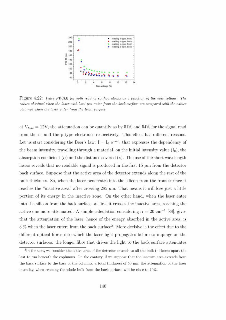
Figure 4.22: Pulse FWHM for both reading congurations as a function of the bias voltage. The
values obtained when the laser with =1 m enter from the back surface are compared with the values
obtained when the laser enter from the front surface.
at Vbias = 12V, the attenuation can be quantify as by 51% and 54% for the signal read
from the n- and the p-type electrodes respectively. This eect has dierent reasons.
Let us start considering the Beer's law: I = I0 eαx, that expresses the dependency of
the beam intensity, travelling through a material, on the initial intensity value (I0), the
absorption coecient () and the distance covered (x). The use of the short wavelength
lasers reveals that no readable signal is produced in the rst 15 m from the detector
back surface. Suppose that the active area of the detector extends along the rest of the
bulk thickness. So, when the laser penetrates into the silicon from the front surface it
reaches the \inactive area" after crossing 285 m. That means it will lose just a little
portion of its energy in the inactive zone. On the other hand, when the laser enter
into the silicon from the back surface, at rst it crosses the inactive area, reaching the
active one more attenuated. A simple calculation considering = 20 cm1 [88], gives
that the attenuation of the laser, hence of the energy absorbed in the active area, is
3 % when the laser enters from the back surface2. More decisive is the eect due to the
dierent optical bres into which the laser light propagates before to impinge on the
detector surfaces: the longer bre that drives the light to the back surface attenuates
2In the text, we consider the active area of the detector extends to all the bulk thickness apart the
last 15 m beneath the coplumns. On the contary, if we suppose that the inactive area extends from
the back surface to the base of the columns, a total thickness of 50 m, the attenuation of the laser
intensity, when crossing the whole bulk from the back surface, will be close to 10%.
140
approximately the laser light by a 50%.
Measurements results are shown in gure 4.21 (b). Comparing the FWHM of the
pulses, as expected, it results practically independent of the surface from which the
laser enters.
4.6 2D position sensitivity and spatial resolution
In order to study the 2D position sensitivity of the new stripixel detector, a simple
(5 points) scan of a pixel has been performed using the same laser setup presented
in section 3.3 and the ALIBAVA DAQ system. Again, a special detector board has
been designed to adapt the detector geometry to the readout electronics. In this case,
the 127 p-type strips have been DC coupled to 127 channels of one Beetle chip, while
two sets of 10 consecutive n-type strips have been AC coupled to the same number
of channels of the other Beetle chip through a capacitor of 2 pF, and biased (10 V)
through a resistor with R = 1M. The other n-type strips have been all bounded3 to
a common bias pad and connected to the same bias circuit through a proper resistor.
The sample bounded to the board was a 2D detector 300 m thick, with pitch
of 80 m, crossed strips and doped polysilicon instead of the rst metal layer (see
section 4.2.2). A picture of the detector mounted on the board is shown in gure 4.23.
4.6.1 Laser characterization
At rst, the laser beam has been positioned to impinge on the detector surface,
approximately in the centre of the pixel dened by two consecutive n-type strips,
among the ones biased and coupled with the readout channels, and two consecutive
p-type strips. Then, it has been moved in other four positions within the pixel.
Due to the nature of the detector, the ALIBAVA DAQ system read out two signals
for each position of the laser: a negative signal from the rst Beetle chip (n-type
strips) and a positive signal from the second Beetle chip (p-type strips). In a detector
characterised by a double-metal connection of the strips, the two signals are supposed
3the wire bonding procedure has been carried out by the High Energy Physics group of the Uni-
versity of Liverpool.
141
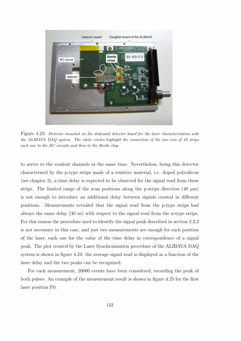
Figure 4.23: Detector mounted on the dedicated detector board for the laser characterisation with
the ALIBAVA DAQ system. The white circles highlight the connection of the two sets of 10 strips
each one to the RC circuits and then to the Beetle chip.
to arrive to the readout channels at the same time. Nevertheless, being this detector
characterised by the p-type strips made of a resistive material, i.e. doped polysilicon
(see chapter 3), a time delay is expected to be observed for the signal read from these
strips. The limited range of the scan positions along the p-strips direction (40 µ m)
is not enough to introduce an additional delay between signals created in different
positions. Measurements revealed that the signal read from the p-type strips had
always the same delay (30 ns) with respect to the signal read from the n-type strips.
For this reason the procedure used to identify the signal peak described in section 3.3.2
is not necessary in this case, and just two measurements are enough for each position
of the laser, each one for the value of the time delay in correspondence of a signal
peak. The plot created by the Laser Synchronisation procedure of the ALIBAVA DAQ
system is shown in figure 4.24: the average signal read is displayed as a function of the
laser delay and the two peaks can be recognized.
For each measurement, 20000 events have been considered, recording the peak of
both pulses. An example of the measurement result is shown in figure 4.25 for the first
laser position P0.
142
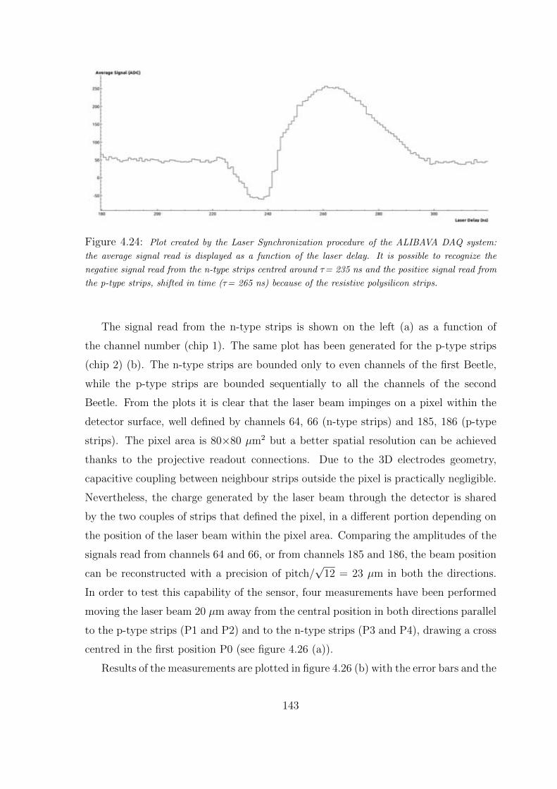
Figure 4.24: Plot created by the Laser Synchronization procedure of the ALIBAVA DAQ system:
the average signal read is displayed as a function of the laser delay. It is possible to recognize the
negative signal read from the n-type strips centred around τ= 235 ns and the positive signal read from
the p-type strips, shifted in time (τ= 265 ns) because of the resistive polysilicon strips.
The signal read from the n-type strips is shown on the left (a) as a function of
the channel number (chip 1). The same plot has been generated for the p-type strips
(chip 2) (b). The n-type strips are bounded only to even channels of the first Beetle,
while the p-type strips are bounded sequentially to all the channels of the second
Beetle. From the plots it is clear that the laser beam impinges on a pixel within the
detector surface, well defined by channels 64, 66 (n-type strips) and 185, 186 (p-type
strips). The pixel area is 80 × 80 µ m2 but a better spatial resolution can be achieved
thanks to the projective readout connections. Due to the 3D electrodes geometry,
capacitive coupling between neighbour strips outside the pixel is practically negligible.
Nevertheless, the charge generated by the laser beam through the detector is shared
by the two couples of strips that defined the pixel, in a different portion depending on
the position of the laser beam within the pixel area. Comparing the amplitudes of the
signals read from channels 64 and 66, or from channels 185 and 186, the beam position
can be reconstructed with a precision of pitch/√
12 = 23 µ m in both the directions.
In order to test this capability of the sensor, four measurements have been performed
moving the laser beam 20 µ m away from the central position in both directions parallel
to the p-type strips (P1 and P2) and to the n-type strips (P3 and P4), drawing a cross
centred in the first position P0 (see figure 4.26 (a)).
Results of the measurements are plotted in figure 4.26 (b) with the error bars and the
143

(a) (b)
Figure 4.25: Measurement results: (a) Signal read from the n-type strips (zoom around the channels
of interest. (b) Signal read from the p-type strips (zoom around the channels of interest).
nominal position of the laser beam. The only result that does not include the expected
value into its error bars is related to the measurement of position P2. Observing the
schematics in gure 4.26 (a) and remembering what presented in chapter 2, the issue
can be due to the orography of the detector surface in the zone of the p-stop ring, that
can have cause a stronger refraction of the laser light changing its trajectory.
Finally, signals from the n-type strips results to be lower than the signals read from
the p-type strips (gure 4.25). Due to the necessity of decoupling the high voltage
supply from the readout chip, the n-type strips are AC coupled with the Beetle channels
through a 2 pF capacitor. From the electrical characterization, we know that the
capacitance of one strip to the bulk is of the same order, that can explain a loss of
signal at the entrance of the readout electronics.
4.7 Summary and discussion
The study presented in this chapter represents the rst experience in producing
and characterizing dual-column 3D stripixel detectors. The stripixel concept was for-
mulated and present by Z.Li almost 10 years ago, when he started investigating the
possibility of obtaining a 2D position-sensitive device by a single-sided fabrication pro-
cess (pixel detector), that could be coupled and readout with a moderate number of
electronic channels (double-strips detector). At rst, the idea was integrated in planar
detectors by means of double-metal layer technology, then the interest in radiation-
144
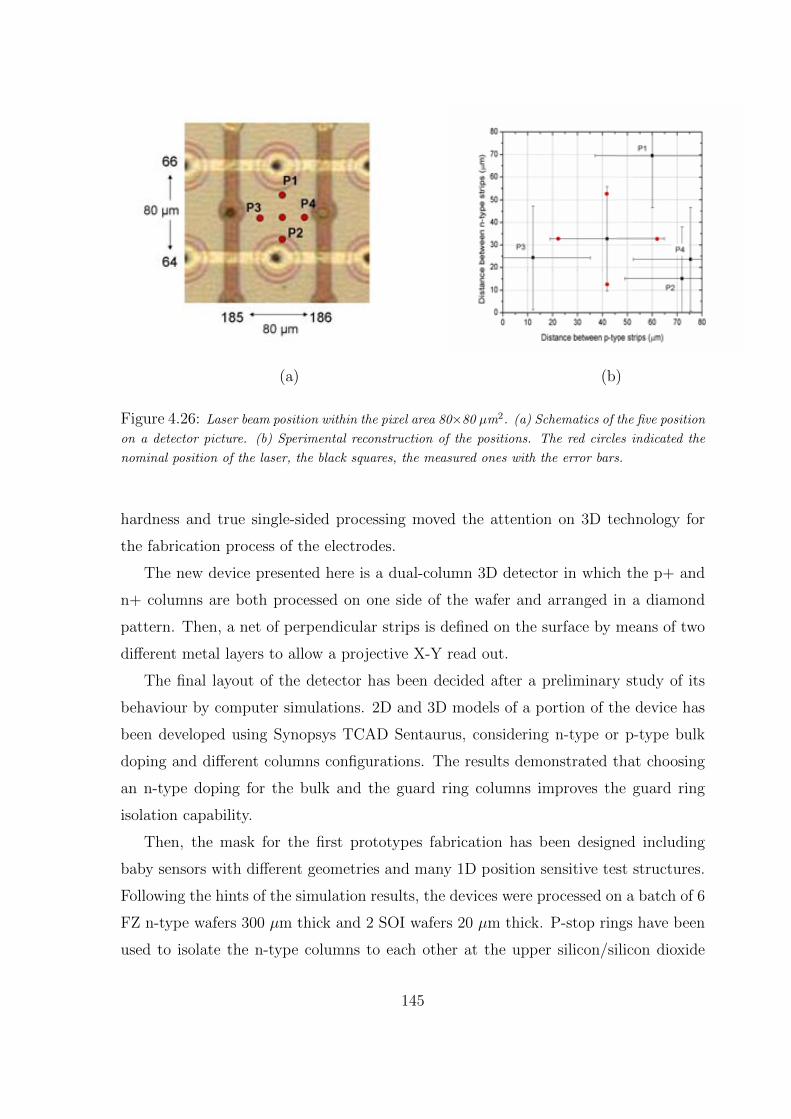
(a) (b)
Figure 4.26: Laser beam position within the pixel area 80× 80 µ m2. (a) Schematics of the five position
on a detector picture. (b) Sperimental reconstruction of the positions. The red circles indicated the
nominal position of the laser, the black squares, the measured ones with the error bars.
hardness and true single-sided processing moved the attention on 3D technology for
the fabrication process of the electrodes.
The new device presented here is a dual-column 3D detector in which the p+ and
n+ columns are both processed on one side of the wafer and arranged in a diamond
pattern. Then, a net of perpendicular strips is defined on the surface by means of two
different metal layers to allow a projective X-Y read out.
The final layout of the detector has been decided after a preliminary study of its
behaviour by computer simulations. 2D and 3D models of a portion of the device has
been developed using Synopsys TCAD Sentaurus, considering n-type or p-type bulk
doping and different columns configurations. The results demonstrated that choosing
an n-type doping for the bulk and the guard ring columns improves the guard ring
isolation capability.
Then, the mask for the first prototypes fabrication has been designed including
baby sensors with different geometries and many 1D position sensitive test structures.
Following the hints of the simulation results, the devices were processed on a batch of 6
FZ n-type wafers 300 µ m thick and 2 SOI wafers 20 µ m thick. P-stop rings have been
used to isolate the n-type columns to each other at the upper silicon/silicon dioxide
145
interface. Two metal layers have been used to contacts the electrodes and allow a
projective X-Y read out on the detector surface.
The nished samples have been electrically characterized in the IMB-CNM labo-
ratory nding that the depletion voltage is lower than 4 V and the leakage current
measured between two strips of opposite doping assumes high values around 10 nA in
detectors 300 m thick.
A test structure with all the n-type strips shorted together as well as all the p-type
strips, has been characterized using a laser Transient Current Technique with lasers
of dierent wavelengths and penetration depths, in a range of voltages between 0V
and 15V. The whole thickness of the bulk and the regions close to the silicon /oxide
interfaces have been investigated conrming that the lateral depletion voltage is less
than 4 V. Signals have been read from both n- and p-type strips. No signal is produced
when the laser cross only the last 15 m under the columns.
2D sensitivity has been tested by scanning the surface of a pixel with a laser and
reading separately the strips crossing the interesting area. The ALIBAVA DAQ system
was used to read out the sensor. Measurements have shown that the laser beam induces
a signal only in two pairs of strips, the two p-type and two n-type strips that dene
the pixel area, almost without charge sharing outside the pixel. The position of the
laser inside the pixel can be reconstructed with a resolution of pitch/p
12 = 23 m in
both the directions.
As mentioned in section 1.2.1, crossed readout strips with a 90 angle lead to
multi-hit ambiguity at high hit density. This design has been chosen here in order
to simplify the structures, focusing the attention on the double-columns and double-
metal layer technologies. The investigation carried out demonstrates the feasibility of
both technologies, however revealing the diculties one has to face dealing with such
complicated processes.
Nevertheless, small-angle stereo can be used in this structures as well as a dierent
arrangement of the electrodes, like those proposed by Z.Li [77], can be designed in
order to further improve the detector capabilities.
146

Chapter 5
Conclusions
The work presented in this thesis deals with the development of innovative tech-
nologies of silicon radiation detectors for future tracker systems. Three types of device
have been studied and designed with the help of dierent tools for computer simula-
tions (Spectre by Cadence and Sentaurus TCAD). They have been manufactured in
the clean room facilities of IMB-CNM in Barcelona and characterized with proper ex-
perimental set-ups in order to test both the detectors capabilities and the quality and
suitability of the technology used for their fabrication process.
In chapter 2 the upgrade of dedicated sensors for the laser alignment of future
tracker systems has been presented. The layer composition of silicon trackers allows
track reconstruction with a precision that depends both on the precision of the sen-
sible elements involved and on the stability of the whole system. Considering the
technological state of the art, stability can only be reached with a precise monitoring
of reciprocal positions between sensible elements in dierent layers. A laser alignment
system provides a solution without additional costs or mass to the system. Following
the successful experiences of the AMS and CMS experiments, the design and technol-
ogy of single-sided silicon microstrip p+-in-n detectors have been slightly modied and
monitored in order to improve IR light transmittance through the detectors volume.
An optical model of the detector has been developed by the IFCA group of experi-
mental physics in Santander and the passage of infra-red light through the sensor has
been simulated, nding the geometrical and technological parameters that could boost
light transmittance. The design and fabrication process of prototype baby sensors
have been carried out at IMB-CNM of Barcelona respecting the hints of the simulation
147

study and the baseline pitch width of 50 m xed by the SiLC collaboration. The
metal strip electrodes have been narrowed in order to meet the optimal width/pitch
ratio ( 10%) that enhance light transmittance without interfering with the diode
structures (p+ implants) of the sensors. A circular window has been opened in the
back metal contact, to allow the laser beam passing through, towards the next sensor
to be aligned. The fabriction process has been monitored in order to measure the thik-
ness of the dielectric layers grown or deposited on the silicon surfaces and to perform
optical measurements with the aim of further improving the simulation model of the
detector and the predicted transmittance of laser light. The last passivation layer of
silicon nitride deposited on both sides of the detector resulted to play a key rule as an
Anti-Re ecting Coating.
The main goals reached by this project are:
A maximum transmittance of 50% for metal-strip-width/pitch ratio of 6% and
a peak value of 80% in unpatterned structures. Results are stable even after
irradiation with 1 MeV neutrons at a uence of 11015 n/cm2.
Uniformity of the optical characteristics, i.e. the technological parameters, within
6 wafers, each one populated by 12 sensors, is better than 5%, that ensure the
possibility of large scale production of the detectors.
The upgrade of the detectors has been carried out slightly changing the design
and the standard technology of common silicon microstrip detectors, obtaining a
similar simple and cheap device.
An optical model of a real microstrip detector and the simulation of the passage
of an IR laser beam through its active volume have been developed, obtaining
coherent predictions of the measured transmittance in the real prototypes. The
model is then validated as a powerful tool for possible future detector upgrade.
In chapter 3 a new 2D position sensitive detector has been presented based on the
standard technology of single-sided AC coupled, silicon microstrip detectors in which
resistive coupling electrodes have been integrated. The metal electrodes on each strip
have been replaced with highly doped polysilicon strips and each electrode has been
double read out. With this conguration, the resistive charge division method can
148

be applied to obtain spatial information on the coordinate of an ionizing event along
the strip length. Optimal results can be achieved when using a readout electronics
with optimal shaping time and electrodes resistance much higher than the preamplier
impedance, as reported by Radeka in 1984. The orthogonal coordinate can be obtained
by using the usual cluster-nding algorithms for microstrip detectors. On the other
hand, when a current signal travels along a resistive electrode (a diusive RC line), it
undergoes both an amplitude attenuation and an increase of the rise time the further
it travels and the higher the resistance of the electrode. Amplitude attenuation allows
to use the resistive charge division method, increasing rise time has to be taken into
account when coupling the detector with a front-end electronics characterized by a nite
integration constant and a short shaping time. Two prototypes of p+-in-n detectors
with strips 20 mm long and dierent electrode linear resistance ( R/l=2.8 /m and
12.2 /m) have been studied and fabricated. In order to study the performance of
the novel detector when coupled with a fast readout electronics, electrical models of the
two prototypes equivalent circuits have been developed. The propagation of a current
signal with initial rise time = 2ns has been simulated with Spectre by Cadence when the
pulse generator is connected to dierent points along an implant length. Both ends of
the coupled resistive electrode were connected each one to a charge preamplier and an
CR-RC shaper with shaping time of 25 ns. A systematic non constant ballistic decit
has been observed aecting the linearity of the sensor response: the eect increases for
higher resistive electrode. The sensors have been fabricated processing the electrodes
during the processes steps, and using the mask level, dedicated to the bias resistances
denition. The electrode resistivity on each wafer has been dened by doping the
polysilicon with dierent Boron concentrations. The real prototypes have been nally
characterized at the IFCA clean room facility in Santander, performing a longitudinal
scan of a strip with a collimated near infra-red laser. The sensors were read out with
the ALIBAVA DAQ system, based on the Beetle ASIC, the front end chip developed
for the tracking system of LHCb at CERN and characterized by a peaking time of
25 ns. Each side of the strips was connected to a readout chip. The results of the
characterization demonstrate that the resistive charge division method is suitable for
silicon microstrip detectors with resistive electrodes, although high resistance lead to
the same non constant ballistic decit foreseen by the simulation study.
149

The most relevant results of this rst investigation are:
2D position sensitive silicon detectors based on the resistive charge division
method can be obtained by means of the standard single-sided fabrication pro-
cess of AC coupled microstrip detectors, simply designing the proper patterns in
the mask levels dedicated to the bias resistor denition.
Decoupling the restive electrode from the strip implants, the resistance value
of the electrode can be opportunely selected in accordance with the electronic
shaping time, without aecting the diode structure of the strip. The simple
simulation model developed in this thesis, and validated by the experimental
results, can be used for future optimization of these parameters.
Spatial resolution along the strip length strictly depends on the S/N, that suers
the eects of the amplitude attenuation as well as of the internal and external
noise sources. In the case of the two prototypes studied here, the achieved spatial
resolution for a 6MIPs signal have been 1.1% and 1.2% of the total strip length
for the detector with less and more resistive electrodes respectively.
The possibility of driving the wire bonding pads to the same edge of the detector,
allowing the use of just one readout chip, has been also investigated running in the de-
tection of undesirable induced signals in the metal lines composing the driving system.
Specic studies on detection of minimum ionizing particles (irradiation at neutron fa-
cilities, beam tests) are in progress to assess its soundness as tracking technology for
the future particle physics experiments, for the particular case of the external layers
of the tracking system in order to improve the tracks reconstruction of the common
single-sided strip detectors. Nevertheless, in its current conception, this implementa-
tion appears as a suitable technology for highly ionizing particles as it is the case of
neutron monitors based on conversion layers or other nuclear imaging technologies,
ranging from Compton cameras to heavy-ion detection.
Finally, chapter 4 relates the new design, fabrication and rst characterization of
double columns stripixel detectors. The stripixel concept was proposed by Z.Li from the
Brookhaven National Laboratory in 2004, when he rstly presented a novel 2D position
sensitive silicon detector based on the planar pixel technology and the integration of
two metal layers on the detector surface to achieve a projective X-U readout typical of
150

double-sided strip detectors. After an attempt of placing both the n+ and p+ planar
electrodes in the same side of the sensor, failed due to the impossibility of depleting the
area beneath the electrodes, 3D detector technology has been considered as a promising
technology for stripixel detectors, upgrading the device to a radiation hard detector.
The new device proposed in this thesis consists of double-column electrodes (both n+
and p+) arranged in a diamond conguration on one side of the n-type silicon bulk and
connected by two sets of perpendicular strips, organized in two separated metal layers,
that allow a X-Y projective readout of the sensor. The nal design has been achieved
after a computer simulation study of the internal electric eld distribution as a function
of the bulk and electrodes doping type, carried out with Sentaurus TCAD. A multiple
trap distribution model has been used to simulate the defects caused by the saw cut
at the edges of the device. The fabrication run dedicated to the prototypes of these
detectors has been the most complicated ever carried out in the clean room facilities
of the IMB-CNM in Barcelona for what concern radiation detectors processing. The
main challenges have been: performing two consecutive column etching processes on
the same surface of the wafer and using dual-metal technology over such a complicated
structure. Despite of some diculties during the processing ow, some detectors could
be characterized at the end of their fabrication. Electrical characterization allowed to
study the leakage current and the depletion voltage of the detectors. Transient Current
Technique measurements were used to test the low electric eld areas inside the detector
bulk and the readout capability from both type of columns. Finally, the same laser
set-up used to characterized the new detectors with resistive electrodes has been used
to test the 2D position sensitivity of this detector too. This work represents the rst
fabrication experience and characterization of 3D stripixel detectors. The main results
obtained can be summarized as follow:
A novel 2D position sensitive 3D detector, based on a real single-sided process,
has been developed with the use of double-column and dual-metal technologies.
The detector is characterized by low depletion voltage (<4V) even if low electric
eld areas always can be observed in the bottom of the bulk, expecially beneath
the n-type columns. The last few microns of the bulk never deplete.
2D position sensitivity has been demonstrated reconstructing a laser beam po-
sition within a pixel (8080 m2) dened by two consecutive p+-type strips
151

crossing two consecutive n+-type strips, with a spatial resolution of 23 m, due
to the low charge sharing between neighbouring strips.
3D detectors are promising devices for application in the innermost layers of track-
ing systems and in the pixel vertex detectors at the future colliders facilities, due to
their higher radiation hardness compared to planar detectors. Actually, both CMS
and ATLAS are investigating the possibility of replacing the current vertex detectors
with 3D pixel detectors. Although, short strip detectors have been proposed for the
innermost layers of the tracking systems.
Conceptually, 3D stripixel detector can be an alternative for those layers where
high radiation hardness is required, but channel occupancy does not put too strong
constraints on the electrode design: for instance, the external layers of vertex detectors
or the innermost layer of the tracking systems. In practice, apart of the diculties
and costs required by their fabrication process, introducing a proper arrangement of
the electrodes and/or stereo-angle between p+-type and n+-type strips is mandatory
to achieve good performance of the device.
152

Bibliography
[1] F. Gianotti, M. L. Mangano, T. Virdee, S. Abdullin, G. Azuelos, A. Ball, et al.
\Physics potential and experimental challenges of the LHC luminosity upgrade" Eu-
ropean Physical Journal C, 39(3), 293 333, 2005.
[2] The web page of ILC is: http://www.linearcollider.org/.
[3] L. Evans and B. Philip, \LHC machine", Journal of Instrumentation, 3(08),S08001,
2008.
[4] B.Wittmer et al., \The Laser Alignment System for the CMS Silicon Microstrip
Tracker", Nucl. Instr. and Meth. A581 (2007)
[5] The ATLAS collaboration. The ATLAS experiment at the CERN Large Hadron
Collider. Journal of Instrumentation, 3(08), S08003, 2008.
[6] M. Moll., \Development of radiation hard sensors for very high luminosity colliders
- CERN-RD50 project" Nucl. Instr. and Meth. A 511(1-2), 97-105, 2003.
[7] T. Blass et al., The SiLC Collaboration, \SiLC: Silicon Tracking for the Linear
Collider", PRC R&D 03/02 proposal submitted to the PRC-DESY, April 10 2003,
and addendum: PRC R&D 03/02 update 01 (03), and references therein. See also:
http://www.desy.de/f/prc/html/documentation.htm
[8] Centro Nacional de Microelectronica, Campus Universidad Autonoma de
Barcelona. 08193 Bellaterra (Barcelona), Spain (http://www.imb-cnm.csic.es/).
[9] Instituto de Fsica de Cantabria Edicio Juan Jorda, Avenida de los Castros, s/n
E-39005 Santander, Cantabria, Spain (http://www.ifca.unican.es/).
[10] G.Lutz \Semiconductor Radiation Detectors: Device Physics", Springer, 1999.
i
[11] S.M.Sze \Semiconductor devices", Ed. Wiley Interscience, 1985.
[12] H.Spieler \Semiconductor detector system", Oxford Science Pubblications, 2005.
[13] S. Ramo, \Currents induced by electron motion", Proc. IRE 27, 584585, 1939.
[14] W.R. Leo, \Techniques for nuclear and particles physics experiments", Springer
Verlag, 1994.
[15] R. Turchetta, \Spatial resolution of silicon microstrip detectors", Nucl. Instr. and
Meth. A 335 (1993) 44-58.
[16] S.I. Parker et al., \3D - A proposed new architecture for solid-state radiation
detectors", Nucl. Instr. and Meth. A 395 (1997) 328-343.
[17] G. Pellegrini, M.Lozano, M. Ullan, R. Bates, C. Fleta and D. Pennicard. \First
double-sided 3D detectors fabricated at CNM-IMB.", Nucl. Instr. and Meth. A 592(1-
2), 38-43, 2008.
[18] V. A.Wright et al., \Three-dimensional Medipix - a new generation of X-ray de-
tectors", IEEE Trans. Nucl. Sci., 52(5), 1873-1876, 2005.
[19] J. Morse, C. J. Kenney, E. M. Westbrook, I. Naday, and S. I. Parker. \The spatial
and energy response of a 3D architecture silicon detector measured with a synchrotron
X-ray microbeam", Nucl. Instr. and Meth. A, 524(1-3), 236-244, 2004.
[20] C. Piemonte. \Device simulations of isolation techniques for silicon microstrip
detectors made on p-type substrates" IEEE Trans. Nucl. Sci., 53(3), 1694-1705, 2006.
[21] C.Fleta, \Tecnologa de detectores de partculas de silicio resistentes a la radiacin",
PhD Thesis, Barcelona 2006.
[22] L. Evensen, A. Hanneborg, B. S. Avset, and M. Nese, \Guard ring design for
high-voltage operation of silicon detectors", Nucl. Instr. and Meth. A 337(1) 4452,
1993.
[23] C.J. Kenney et al., \Active-edge planar radiation sensors", Nucl. Instr. and Meth.
A 565(1) (2006) 272-277.
ii

[24] J. Kemmer, \Fabrication of low Noise Silicon Radiation Detectors by the Planar
Process", Nucl. Instr. and Meth. A 169 (1980) 499-502.
[25] C. Adolphsen et al., \The Mark II silicon strip vertex detector", Nucl. Instr. and
Meth. Phys. Res. A 313 (1992) 63-102.
[26] The web page of LEP is: http://public.web.cern.ch/public/en/research/lep-
en.html;
[27] G. Batignani et al. \The ALEPH silicon vertex detector", Nucl. Phys. B, Proc.
Suppl. 23 (1991) 291-296.
[28] N. Bingefors et al., \The DELPHI microvertex detector", Nucl. Instr. and Meth.
A 328 (1993) 447
[29] P.P. Allport et al., \The OPAL silicon strip microvertex detector with two coordi-
nate readout" Nucl . Instr. and Meth . A 324 (1993) 34.
[30] M. Acciarri et al., \The L3 silicon microvertex detector", Nucl . Instr. and Meth.
A 351 (1994) 300-312.
[31] A. Sill for the CDF collaboration, \CDF Run II Silicon Tracking Projects", Nucl
. Instr. and Meth. A447 20001.
[32] The web page of KEK is: http://legacy.kek.jp/intra-e/.
[33] Stanford Linear Accelerator Center, http://www.slac.stanford.edu/.
[34] Inner Tracker Technical Design Report. CERN/LHCC 2002-
029 LHCb TDR 008 November 8, 2002, available at:
http://lhcb.web.cern.ch/lhcb/TDR/front%20cover/LHCb-IT-TDR.pdf.
[35] The web site of the TOTEM collaboration is: http://totem.web.cern.ch/Totem/.
[36] \Alice Technical Design Report of the Inner Tracking System (ITS)",
CERN /LHCC 9912 ALICE TDR 4, 18 June 1999 available at:
http://aliceinfo.cern.ch/ITS/sites/aliceinfo.cern.ch.ITS/les/documents/ITS-
TDR.pdf.
iii

[37] W. Wallra, \TAS status", AMS Tracker Meeting, CERN, February 9th 2005.
[38] F. Taccetti et al., \Pamela tracking system: status report", Nucl. Instr. and Meth.
A 485 (2002) 7883.
[39] The web page of GLAST is: http://www-glast.slac.stanford.edu/tracker-
hardware/publications/c5-paper.pdf.
[40] The web page of CERN is: www.cern.ch.
[41] The RD50 Collaboration, RD50 Status Report 2008, CERN-LHCC-2010-012 and
LHCC-SR-003.
[42] The RD50 Collaboration web page is: /http://rd50.web.cern.ch/rd50S.
[43] M. Fernandez et al., \R&D on Microstrip IR Transparent Silicon Sensors" Eu-
det Memo 2007-32 available at: http://www.eudet.org/e26/e28/e182/e428/eudet-
memo-2007-32.pdf.
[44] B. Dhoedt, D. Delbeke, \RODIS: Rigorous Optical Diraction Software",
http://www.photonics.intec.ugent.be/research/facilities/design/rodis/.
[45] P. Bienstmann, L. Vanholme, \CAMFR: Cavity Modelling Framework",
http://camfr.sourceforge.net/.
[46] E.D. Palik, \Handbook of Optical Constants of Solids", Academic Press. 1st edition
(January 15, 1997).
[47] M.J. Keevers, M.A. Green, \Absorption edge of silicon from solar cell spectral
response measurements", Appl.Phys.Lett. 66 (2), 174-176, 9 January 1995
[48] S. E. Aw, H. S. Tan and C. K. Ong, \Optical absorption measurements of band-gap
shrinkage in moderately and heavily doped silicon" J. Phys. Condens Matter 3 (1991)
8213-8223.
[49] M. Fernandez et al., \Experimental validation of optical simula-
tions for microstrip detectors" Eudet Memo 2008-37 available at:
http://www.eudet.org/e26/e28/e615/e838/eudet-memo-2008-37.pdf
iv

[50] M. Fernandez et al., \New silicon microstrip detectors optimized for tracker align-
ment" Nucl. Instr. and Meth. A A624(2010)340343.
[51] T. Bergauer et al., \Results from a rst production of enhanced silicon sensor Test
Structures produced by ITE Warsaw", Nucl . Instr. and Meth A 598 (2009) 86-88.
[52] The TOPSIL web page is: http://www.topsil.com/1.
[53] Carlos Martinez \Desarrollo de una tecnologa de detectores de radiacin de silicio
de micropistas para aplicaciones de fsica de altas energas", PhD Thesis, Barcelona
2003.
[54] H.Xiao \Introduction to Semiconductor Manifacturing Technology", Prentise Hall
(2001).
[55] D.Bassignana et al. \Silicon microstrip detectors for future tracker alignment sys-
tems", Nucl. Instr. and Meth. A 628, 276-281.
[56] A. Chilingarov, \Recommendations towards a standardisation of the macroscopic
parameter measurements", Technical note 2003/03, RD50 (2003), available at:
http://rd50.web.cern.ch/rd50/.
[57] Near Infrared Spectrometer, NIR 512L-1.7T1 USB, 523 element InGaAs, single
stage TE cooled, Control Development, http://www.controldevelopment.com
[58] J. Stefan Institute, Jamova cesta 39, 1000 Ljubljana, Slovenia, http://www.ijs.si/.
[59] D.Bassignana et al., \First investigation of a novel 2D position-sensitive semicon-
ductor detector concept" 2012 JINST 7 P02005.
[60] H. Foeth, R. Hammarstrom, C. Rubbia, \On the localization of the position of the
particle along the wire of a multiwire proportional chamber", Nucl. Instr. and Meth.
109 (1973) 521.
[61] P. Schubelin, et al., \Low mass cylindrical multiwire proportional chamber with
unambiguous dual coordinate readout", Nucl. Instr. and Meth. 131 (1975) 39.
v

[62] A. Feinberg, N. Horwitz, I. Linscott, G. Moneti, \A Frameless, Cylindrically
Shaped, Multiwire Proportional Chamber Using Charge Division Readout", Nucl.
Instr. and Meth. A 141 (1977) 277.
[63] V. Radeka, P. Rehak, \Charge Dividing Mechanism on Resistive Electrode in
Position-Sensitive Detectors", IEEE Transactions on Nuclear Science NS-26 (1979)
225.
[64] R.B. Owen, M.L. Awcock, \One and Two Dimensional Position Sensing Semi-
conductor Detectors", IEEE Transactions on Nuclear Science NS-15 (1958) 290.
[65] V. Radeka, \Signal, Noise and Resolution in Position-Sensitive Detectors, IEEE
Transactions on Nuclear Science NS-21 (1974) 51.
[66] J. K. Carman, et al., \Longitudinal resistive charge division in multi-channel sili-
con strip sensors", Nucl. Instr. and Meth. A 646 (2011) 118.
[67] R.Marco-Hernandez and ALIBAVA collaboration, \A Portable Readout System
for Microstrip Silicon Sensors (ALIBAVA)", IEEE Transactions on Nuclear Science
NS-56 (2009) 1642.
[68] Beetle - a readout chip for LHCb http://www.kip.uni-heidelberg.de/lhcb/.
[69] N. Bacchetta et al. , \SPICE analysis of signal propagation in Si microstrip de-
tectors", IEEE Transactions on Nuclear Science NS-42 (1995) 459.
[70] Virtuoso Spectre data sheet, Cadence. Available at
http://www.cadence.com/products/custom ic/index.aspx.
[71] R. Brun et al., \ROOT An Object-Oriented Data Analisis Framework". Available
at http://root.cern.ch/drupal/.
[72] Alibava-gui documentation. Available at http://twiki.ic.uv.es/twiki/pub/Atlas/ALiBaVa/.
[73] J.C.Vermeulen \Noise in resistive charge-division position-sensing methods". Nu-
clear Instruments and Methods in physics Research A 185 (1981) 591-593.
[74] http://www.bnl.gov/world/.
vi

[75] Z.Li, \Novel silicon stripixel detector: concept, simulation, design, and fabriction",
Nuclear Instruments and Methods in Physics Research A 518 (2004) 738-753.
[76] Z.Li, \New 3d Si Detectors at BNL and CNM", 2006 IEEE Nuclear Science Sym-
posium Conference Record N34-5.
[77] Z.Li, \Development, simulation and processing of new 3D detectors", Nuclear In-
struments and Methods in Physics Research A 583 (2007) 139-148.
[78] R. Nouicer et al. \PHENIX Upgrade: Novel Stripixel Detector for Heavy Quark
Detection and Proton Spin Structure Measurements at RHIC Energies", Nuclear
Instruments and Methods in physics Research B 261 (2007) 1067-1071.
[79] R. Nouicer at al. \Status and Performance of New Silicon Stripixel Detector for
the PHENIX Experiment at RHIC: Beta Source, Cosmic-rays and Proton Beam at
120 GeV", 2009 JINST 4 P04011.
[80] Synopsys TCAD Sentaurus, http://www.synopsys.com/tools/tcad/Pages/default.aspx.
[81] W. Fichtner, D. J. Rose, and R. E. Bank. \Semiconductor device simulation",
IEEE Trans. Electron Dev., 30(9), 1018-1030, 1983.
[82] \Sentaurus Device" Version X-2005.10, October 2005 or \Sentaurus Device User's
Guide" Version E-2010.12, December 2010.
[83] M. N. O. Sadiku. \A simple introduction to nite-element analysis of electromag-
netic problems", IEEE Transactions on Education, 32(2), 85 93, 1989.
[84] E.P. Nochis et al., \Simulation of planaredgeless silicon detectors with a current
terminating structure", Nucl. Instrum. and Meth. A 583(1) (2007) 77-86.
[85] V. Eremin and Z. Li. \Determination of the Fermi Level Position for Neutron Ir-
radiated High Resistivity Silicon Detectors and Materials Using the Transient Charge
Technique (TChT)", BNL 60072. pres. IEEE Nuclear and Space Radiation Eects
Conf., Tucson, AZ. IEEE Trans. Nucl. Sci. NS-41, No. 6, p. 1907 (1994).
[86] V. Eremin, Z. Li, and Ijashenko. \Trapping Induced Neff and Electrical Field
Transformation at Dierent Temperatures in Neutron Irradiated High Resistivity
vii

Detectors", BNL 60154. pres. at Frontier Detectors for Frontier Physics, 6th Pisa
Mtg. on Advanced Detectors, Elba, Italy, 22-28 May (1994). Nucl. Instrum. and
Meth. A360 458 (1995).
[87] V. Eremin, N. Strokan, E. Verbitskaya, and Z. Li. \Development of Transient
Current and Charge Techniques for the Measurement of Eective Impurity Concen-
tration in the Space Charge Region of p-n Junction Detectors", BNL 60156. Nucl.
Instrum. and Meth. A372 (1996) 388-398.
[88] A. H. Johnston. \Charge Generation and Collection in p-n Junctions Excited with
Pulsed Infrared Lasers", IEEE Transactions on Nuclear Science, vol. 40, NO. 6,
december 1993.
[89] Sproul AB, Green MA. \Improved value for the silicon intrinsic carrier concen-
tration from 275 to 375 K", Journal of Applied Physics [Internet]. 1991 70:846-854.
Available from: http://link.aip.org/link/?JAP/70/846/1
viii