New product update: op amps and PSpice(R) for TI
61
New Product Update: General Purpose Op amps and PSpice® for TI Kiernan Farmer and Jerry Madalvanos 9/17/20 1 SLOP410
-
Upload
khangminh22 -
Category
Documents
-
view
4 -
download
0
Transcript of New product update: op amps and PSpice(R) for TI

New Product Update: General Purpose Op amps and PSpice® for TI
Kiernan Farmer and Jerry Madalvanos
9/17/20
1
SLOP410

General Purpose Amplifier Agenda Industry’s largest portfolio of amplifiers that are cost-optimized and simple to use for any application
Innovative
Technologies
Low Voltage
Amps
≤6V
World’s
Smallest
Packages
High Voltage
Amps
16V, 40V+
Standard
Amps
Simulation
Tools
300mm
Manufacturing

TI Amplifiers Investment Areas
High Speed
Products • >50 MHz GBW Op Amps • Fully Differential Amplifiers • Transimpedance Amplifiers • Line Drivers
Focus Markets • Industrial
− Grid Infrastructure
− Test & Measurement
− Aerospace and Defense
− FA&C
• Automotive
− ADAS
− HEV/EV
Mid Power Audio
Amplifiers
Products • Mid Power Audio Amps
• Automotive Audio Amps
• Mid Power Haptics
• High Power Amps
• Automotive High Power
Low Power
Audio and Actuator
Products • Low Power Audio
• Low Power Haptics
• Industrial Piezo Drivers
Focus Markets
• Personal Electronics: − Smartphones − Tablets − Wearables − Portable Speakers
• Automotive Haptics
General Purpose
Products • >1mV VOS Amps
• Low Voltage Gen Purpose
• High Voltage Gen Purpose
• Industry Standard Amps
• HV & LV
• AEC Q100 Amps
Focus Markets • Industrial
− Building Automation
− Factory Automation
− Appliances
− Grid Infrastructure
• Automotive
• Consumer Electronics
• Communications
Precision
Products • <1mV VOS • Class A/B Audio Amps • Instrumentation Amps • Power Amps • XTRs | DIFF Amps | LOGs
Focus Markets • Industrial
− Factory Automation
− Test & Measurement
− Medical
• Professional Audio
• Automotive
Comparators
Products • Low Power Comparators • High Speed Comparators • Low Voltage Comparators • High Voltage Comparators
Focus Markets • IoT • Building Automation • Factory Automation • Consumer Electronics • Automotive
RF - Amps
Products • RF Amps • RF Power Detectors • RF TIAs
Focus Markets • Communications
• Wireless Infrastructure
• Radar
− Military and Aerospace
• Industrial
− Test & Measurement
Focus Markets
• Automotive: − Telematics − Digital Cockpit − External Amplifier
• TV & Soundbars
• Smart Speakers
• Building Automation
• Multimedia Devices
Switching Amplifiers Linear Amplifiers

Wafer Sizes – 300mm Manufacturing 150mm, 200mm, 300mm
Roughly 6”, 8”, and 12” in diameter
• Increased chips per wafer to expand TI’s high
volume analog production
• 125% more area than 200mm
• 300% more area than 150mm
• Multi-fab support to maintain supply continuity
• Assembly sites with 300mm wafer capability

Problems solved
• Today's applications are using denser component spacing, placing mixed-signal
analog and digital devices even closer together. EMI can have detrimental effects
in these systems.
• TI’s amplifiers with EMI Filter inside incorporates an internal input low-pass filter
that reduces the amplifiers response to EMI. Both common-mode and differential
mode filtering are provided by this filter. The filter is designed for a cutoff frequency
outside the bandwidth of the op amp with a roll-off of 20dB per decade.
• Op amps with integrated EMI Filter have better EMI immunity and are more robust
to noise-sensitive application, such as motors and switching power supplies.
Implementation Overview
EMI Filter Overview TLV90xx | OPAx990 | LM358B
AN-1698 A Specification for EMI Hardened Operational Amplifiers
Device Example: EMIRR vs Frequency
Integrated
Comparing EMI Robustness
TLV9002 OPA2990
Improved EMI immunity of an
operational amplifier over a broad
frequency spectrum extending from 10
MHz to 6 GHz.
Reduce the effects of EMI from
sources such as wireless
communications and densely-
populated boards with a mix of analog
signal chain and digital components.

Industry Leading in Tiny Amps
SOIC-8 VSSOP-8 SOT-23-THN
SOIC-14 TSSOP-14 SOT-23-THN-14
4.9 x 6mm 2.9 x 2.8 mm
4.2 x 3.2mm 8.65 x 6mm
TSSOP-8
Package dimensions include leads
Evolution in size – more
functions in smaller spaces
Options for
Industrial & Auto Easy manufacturing
for customers
Broad product
portfolio
3 x 6.4mm
Competitive Edge in Small Packages
Layout compatible options with
industry standard packages
World’s smallest
amplifiers
Down to 0.8 x 0.8mm (1ch), 1.5 x 2mm (2ch),
2 x 2mm (4ch)
Satisfies second-source requirements
for commodity devices
3 x 4.9mm
5 x 6.4mm
Smallest leaded
packages
Meets needs of space-constrained and manufacturing-
constrained industrial & automotive designs
SOT-23-5 SC-70 X2SON
WSON X2QFN
WQFN X2QFN
2.9 x 2.8mm 0.8 x 0.8mm 2.0 x 2.1mm
2 x 2 mm
3 x 3 mm
2 x 1.5 mm
2 x 2 mm

DDF Package leaded SOT23 package | 8 pins | 0.65mm lead pitch
Features Benefits
• Electronic Point of Sale (EPOS)
• Building Automation
• Factory Automation & Control
• Motor Drives
• Digital Camera and Lenses
• Portable Speakers
Applications
• Smallest leaded dual package in Amoeba family
enables a reduced PCB area without requiring QFN
manufacturing techniques
• 0.65mm pin pitch allows for dual-layout techniques
with industry standard SOIC, TSSOP, and VSSOP
packages
• Body Size 1.6 mm x 2.9 mm
• Body + Leads Size 2.8 mm x 2.9 mm
• Lead Pitch 0.65 mm
• Package Height 1.1 mm
• Identical lead pitch as TSSOP, VSSOP
Available Now!
TLV9002 LMV358A OPA2991 TLV9162
TLV9052 LM358B OPA2992 TLV9302
TLV9062 LM2904B TLV9102 TLV9352
LM358LV OPA2990 TLV9152 TLV9362
www.ti.com/smallamp-designguide
DGK to DDF
VSSOP to SOT23-8
PW to DDF
TSSOP to SOT23-8
www.ti.com/smallamps
Same Size as DBV (SOT23-5)

New Devices Package Options
Channel Package Name Designator (pins) Body Size (mm) Package Size (mm) Shutdown
1
X2SON DPW 5 0.8 x 0.8 Same
SOT553 DRL 5 1.6 x 1.2 1.6 x 1.6
SC70 DCK 5 2.0 x 1.25 2.0 x 2.1
SOT23 DBV 5/6 2.9 x 1.6 2.9 x 2.8
2
X2QFN RUG 10 2.0 x 1.5 Same
WSON DSG 8 2.0 x 2.0 Same
SOT23-THIN DDF 8 2.9 x 1.6 2.9 x 2.8
VSSOP DGK
DGS 8/10 3.0 x 3.0 3.0 x 4.9
TSSOP PW 8 3.0 x 4.4 3.0 x 6.4
SOIC D 8 4.9 x 3.91 4.9 x 6.0
4
X2QFN RUC 14 2.0 x 2.0 Same
WQFN RTE 16 3.0 x 3.0 Same
SOT23-THIN DYY 14 5.8 x 1.6 5.8 x 2.8
TSSOP PW 14 5.0 x 4.4 5.0 x 6.4
SOIC D 14 8.65 x 3.91 8.65 x 6.0
Industry
Standard
Small
Package

Problems solved
• As products require longer battery life, the need for lower power solutions is
increasing. Typically, low IQ amplifiers have high noise specs and low GBP. If
these are key specs for your system, using a shutdown amplifier is a solution.
• By using a logic signal to turn the amplifier off between readings, the system
level IQ is reduced significantly. Therefore one could utilize a higher GBW, lower
noise amplifier to obtain the required info. It’s important to consider SHDN enable
and disable times. Typically they are proportional to GBW of the device.
• Aside from the obvious power savings, putting the amplifier into shutdown also
provides a know output state of high-Z. This can be useful in applications where
safety is key, such as medical products or mission-critical applications.
Implementation Overview
Shutdown Overview TLV900xS | TLV905xS | TLV906xS | OPAx990S | OPAx991S
Shutdown: Features and Benefits (releasing soon!)
Specifications TLV900xS
w/ Shutdown
TLV313
w/o Shutdown
SHDN pins Enable IQ=0.5uA IQ=65uA
SHDN pins Disable IQ=60uA IQ=65uA
Total IQ with 10%
Duty Cycle IQ=6.45uA IQ=65uA
Device Example
Advantage
Saves Power
CMOS logic compatible
Default Power ON - NC Acceptable
INP
VCC+
INN
VCC-
EN
OUT +
−
VCC+
VCC- ON OFF ON OFF
Enable Pin Power Cycling
Pin out difference
One Extra pin for Single
Two Extra pins for Dual, Quad
VEN = NC Amplifier Enabled
VEN > (Vcc-)+0.9V Amplifier Enabled
VEN < (Vcc-)+0.7V Amplifier Disabled
OFF
ON
OFF
ON
V+
V-
Min VSHDN_THR_LO (V-)+0.2V
Max VSHDN_THR_HI (V-)+1.1V
(V-)+0.7VTyp VSHDN_THR_LO
Typ VSHDN_THR_HI (V-)+0.9V

General Purpose Amps | Roadmap Overview
Low voltage (VDD < 7V)
High voltage (VDD > 7V)
Standard amps (5V and 36V)
TLV906x 10MHz
10MHz
TL06xH 1MHz,
-40 – 125C
OPAx991 40V, 4.5MHz,
0.675mV, RRIO TL07xH
TL08xH 3MHz, -40–125C
5V standard amplifiers
36V standard amplifiers
LM321LV Single
LM358LV Dual
LM324LV Quad
Optimized for 5V systems
LM358B 1MHz, Dual
-40 – 85C
LM2904B 1MHz, Dual
-40 – 125C
TLV900x 1MHz
1 MHz
TLV915x 16V, 4.5MHz,
0.675mV, RRIO
OPAx990 40V, 1MHz,
1.5mV, RRIO
TLV910x 16V, 1MHz,
1.5mV, RRIO
16V
TLV904x 350kHz, 10uA
350 kHz – Low Iq
OPAx375 10MHz 3.1nV/√Hz
10 MHz - Low noise
TLV935x 40V, 3.5MHz,
1.8mV RRO
TLV930x 40V, 1MHz,
2.5mV, RRO
40V
Sampling Production
Industry Standard Bipolar
1 MHz 1 MHz
3-5 MHz 3-5 MHz JFET/CMOS
TLV905x 5MHz, 15V/us
5MHz– High Slew Rate
16V 40V

Catalog LV Roadmap (1.8V-5.5V) Sampling Production
TLV900x/S | 1MHz RRIO, 1.5mV, 60μA
TLV906x/S | 10MHz RRIO, 1.5mV, 0.75mA
TLV905x/S | 5MHz RRIO, 15V/µs, 0.33mA
OPAx375 | 10MHz RRO, 0.5mV, 3.1nV/√Hz
Diffe
ren
tia
ted
G
en
era
l
Lower Noise
Lower IQ
Higher Slew Rate
OPAx313
TLVx313/TLV600x
OPAx316
TLVx316
OPAx347
OPAx348
OPAx314
TLVx314
TLV904x/S | 350kHz 1.2V Opp. RRIO, 2.2mV, 10uA
TLV674x | 10MHz RRO, 1.5mV, 3.1nV/√Hz

TLV906x: TLV9061 / TLV9062 / TLV9064 10MHz | 300µV typ| 1.8V - 5.5V | World’s Smallest Amplifier
• E-bike Battery management unit
• Currency counters
• Sensors and Signal Conditioning
• ADC Input Driver amplifier
• Medical Instrumentation
Features Benefits
Applications
• World's smallest amplifier package enables robust
performance in tight places
• Rail-to-rail and wide voltage supply capabilities allow for a
versatile range of low voltage applications
• High performance features such as high GBW, low offset,
low noise, and a varying supply voltage operation ease the
burden of selection of finding an all-around op amp
suitable for a variety of applications.
• Low noise enables use in high dynamic range applications
• EMI filtering results in high EMIRR
• 0.8mm x 0.8mm package
• Rail-to-Rail Input and Output
• Wide Bandwidth 10 MHz
• Quiescent Current 538 µA (typ)
• Low Offset 1.6 mV (max)
• Very Low Noise 10 nV/√Hz
• Supply Voltage 1.8 V to 5.5 V
• Extended Temp Range -40C to 125C
• EMI Input Filtered
TLV906x • Low Side Current Sensing
• PCB Layout Guidelines
• Design and Manufacture
with TI’s X2SON Packages

TLV900x: TLV9001 / TLV9002 / TLV9004 RRIO | 1 MHz | 1.8V - 5.5V CMOS Amplifier for Cost-Sensitive Applications
• E-bike Battery management unit
• Currency counters
• Sensors and Signal Conditioning
• ADC Input Driver amplifier
• Medical Instrumentation
Features Benefits
Applications
• Rail-to-rail and wide voltage supply capabilities allow
for a versatile range of low voltage applications
• High bandwidth-1 MHz supports high-speed signal
processing
• Higher cap load drive results in robust solutions w.r.t
stability
• Low noise enables use in high dynamic range
applications
• EMI filtering results in high EMIRR
• Rail-to-Rail Input and Output
• Wide Bandwidth 1 MHz
• High Cap-load Drive 100 pF
• Low Offset 1.5 mV (max)
• Very Low Noise 26 nV/√Hz @ 1kHz
• Quiescent Current 60 µA (typ)
• Supply Voltage 1.8 V to 5.5 V
• Unity Gain Stable
• EMI Input Filtered
Linear IR LED Drive with Temperature Compensation
Amp MCU
PWM / GPIO
2.5V

TLV904x: TLV9041 / TLV9042 / TLV9044 RRIO | 350 kHz | 1.2 V – 5.5 V Low Iq, CMOS Amplifier
Features Benefits
• High bandwidth 350kHz @ Low Quiescent current
• Rail-to-rail and 1.2V minimum voltage supply
capabilities allow for a versatile range of low voltage
applications
• Utilizes innovative output stage to provide high cap-
load drive improves stability across design parameters
• Low noise for low power amplifiers enables use in high
dynamic range applications
• EMI filtering results in high EMIRR
• Rail-to-Rail Input and Output
• Quiescent Current 10 µA (typ)
• Wide Bandwidth 350 kHz
• High Cap-load Drive 75 pF
• Low Offset 3 mV max 375 uV typ
• Low Noise 82 nV/√Hz @ 1kHz
• Supply Voltage 1.2 V to 5.5 V
• Unity Gain Stable
• EMI Input Filtered
• Smoke Detectors
• Motion Detectors
• Wearables
• Sensor Signal Conditioning
• Personal Electronics
Applications
AMPS
1 & 2
AMPS
3 & 4
TLV9044

TLV905x: TLV9051 / TLV9052 / TLV9054 RRIO | 5 MHz | 1.8V - 5.5V CMOS Amplifier for Cost-Sensitive Applications
• HVAC: Heating, Ventilating, and AC
• Photodiode Amplifier
• Current Shunt Monitoring for DC Motor Control
• White Goods (Fridges, Washer/Dryer, Large Appliances)
• Low-Side Current Sensing
Features Benefits
Applications
• RRI allows operation down to 1.8V providing ability to
function slightly below the rail
• High bandwidth-5MHz supports faster settling time
compared to lower GBW amplifiers
• Slew boost technology provides better transient
performance rapid changing inputs
• Low noise enables lower SNR in high-gain sensor
signal conditioning applications
• RC Filtering supply improves EMIRR
• Rail-to-Rail Input and Output
• Wide Bandwidth 5 MHz
• Low Offset +/- 0.35mV (typ)
• Very Low Noise 16 nV/√Hz @ 1kHz
• Quiescent Current 330 µA (typ)
• Fast Slew Rate 15 V/µS
• Supply Voltage 1.8 V to 5.5 V
• Internal RFI & EMI Filter on supply rails
• Extended Temp Range -40ºC to 125ºC
Slew
Limit
Small Signal
Step Response

Slew Boost Overview TLV905x | OPAx991 | TLV915x | TLV935x
Problems solved
• A typical amplifier has an input stage and an output stage with a compensation capacitor (Cc). Its slew rate is determined by the maximum current (iout) available to charge Cc.
• TI’s Slew Boost topology senses large signal inputs and switches in
another current source (isb) to increase the amount of current available for charging Cc.
• Slew boosted op amps have better transient performance in applications
with rapidly changing inputs or discontinuous signals such as motor control and current sensing.
Implementation Overview
Slew Boost: Features and Benefits (releasing soon!)
Specifications Slew Boosted
TLV905x
Non-Slew
Boosted
OPAx377
Slew Rate (V/µs) 15 2
GBW 5 MHz 5.5 MHz
Supply Current (Iq) 330 µA 1050 µA
Device Example:
Slew
Limit
Small Signal
Step Response
• Improved slew rate
performance for a given
device bandwidth and
current consumption.
• Decreased settling time
for large signal inputs

OPAx375: OPA375 / OPA2375 / OPA4375 RRO | 10MHz | 1.8V – 6.0V | Low Noise, CMOS Amplifier
• Smoke Detectors
• Infotainment Audio applications
• Sensors and Signal Conditioning
• ADC Input Driver amplifier
• Medical Instrumentation
Features Benefits
Applications
• Low Noise enables high gain configurations to amplify
weak sensor signals
• High bandwidth-10MHz supports high-speed signal
processing
• Higher cap load drive results in robust solutions w.r.t
stability
• Low noise enables lower SNR in high-gain sensor
signal conditioning applications
• EMI filtering results in high EMIRR
• Very Low Noise 3.7 nV/√Hz @ 10k
• Wide Bandwidth 10 MHz
• High Cap-load Drive 50 pF
• Low Offset 500 µV(max)
• Quiescent Current 980 µA (typ)
• Supply Voltage 1.8 V to 6.0 V
• Max Vos Drift 2.0 µV / °C
• Rail-to-Rail Output
• Unity Gain Stable
VEE
VCC
+
0.9V bias generator
OUT-
++3
2
6
74
TLV6741
5p
10MEG
Sensor Capacitance 2n
Sensor resistance 10MEG OPAx375

TLV674x: TLV6741 / TLV6742 / TLV6744 RRO | 10MHz | 1.8V - 5.5V Low Noise, CMOS Amplifier
• Medical Sensor Signal Conditionings
• Microphone pre amplifiers
• Infotainment Systems
• ADC Input Driver amplifier
• Currency counters
Features Benefits
Applications
• Low Noise enables high gain configurations to amplify
weak sensor signals
• High bandwidth-10MHz supports high-speed signal
processing
• Higher cap load drive results in robust solutions w.r.t
stability
• Low noise enables use in high dynamic range
applications
• EMI filtering results in high EMIRR
• Very Low Noise 3.7 nV/√Hz
• Wide Bandwidth 10 MHz
• High Cap-load Drive 50 pF
• Low Offset 1 mV (max)
• Quiescent Current 960 µA (typ)
• Supply Voltage 1.8 V to 5.5 V
• Rail-to-Rail Output
• Unity Gain Stable
• EMI Input Filtered
VEE
VCC
+
0.9V bias generator
OUT-
++3
2
6
74
TLV6741
5p
10MEG
Sensor Capacitance 2n
Sensor resistance 10MEG

Catalog HV Roadmap 3
6-4
0V
Ca
talo
g
TLV930x | 1MHz 40V, 1 MHz, RRO, 2.5mV, 150uA
TLV935x | 3.5MHz 3.5 MHz, RRO, 1.5mV, Low cost
16
V C
ata
log
OPAx990 | 1MHz 40V 1.1 MHz, RRIO, 1.4mV, 120uA
OPAx991 | 4.5MHz 4.5 MHz, RRIO, 650uV, High slew
TLV910x | 1MHz 1.1 MHz, RRIO, 1.4mV, 120uA
TLV915x | 4.5MHz 4.5 MHz, RRIO, 650uV, High slew
Sampling Production
LM613x
TLE207x
LMC7101/LMC6xx
LM7301
OPAx17x
TLE216x
TLVx17x
TLV27x
TLV237x
1 MHz 3-5 MHz

OPAx990: OPA990 / OPA2990 / OPA4990 RRIO | 1.1MHz | 1.5mV | MUX-friendly | 2.7V - 40V CMOS amplifier
Features Benefits
Applications
• Full common-mode input range over a wide supply
gives consistent performance for many configurations
• Strong output current and cap load drive with low
settling time ideal for ADC-driving applications
• Low noise and THD+N improves dynamic range
• Industry-leading slew rate for IQ enables
applications with fast transients and step responses.
• EMI filtering for robust performance in noisy
environments
• Rail to rail input and output
• Wide bandwidth 1.1 MHz
• Low offset 0.3mV/1.5mV(typ/max)
• Low offset drift 0.6µV/°C
• Very low noise, THD+N 28 nV/√Hz, 0.00162%
• Quiescent current 120 µA (typ)
• High output current 80mA (typ)
• High slew rate 4.5V/µs
• Cap load drive 100pF
• MUX-friendly inputs No back-to-back diodes
• Excellent EMIRR 72dB
• Optical modules and networking
• Test & measurement
• Grid infrastructure
• Industrial automation
• Industrial, telecom, and server power delivery
MUX-friendly inputs give much faster
settling time when interfaced with MUX

MUX-Friendly Input Overview OPAx99x | TLV93xx | TLV91xx| OPA189 | OPA19x
Problems solved
• Most high voltage amplifiers have back-to-back diodes connected
between the inputs of the amplifier for front-end protection. These
protection diodes introduce a significant settling time delay in
multiplexed applications.
• When switching between input channels, the MUX observes a full-
scale step change. This forces the input protection diodes to turn
ON and draw large currents.
Settling Issues in Multiplexed Signal Chain Overview
Much faster settling time when interfaced
with MUX
• 16-bit, differential four-channel
multiplexed DAQ system
• 400-kSPS throughput
• Differential input of ±20V
• Integral nonlinearity (INL) < ±0.9 LSB
• Channel-to-channel settling< ±1.2 LSB
MUX-Friendly Features & Benefits:
MUX-friendly precision operational amplifiers

TLV910x: TLV9101 / TLV9102 / TLV9104 RRIO | 1.1MHz | 1.5mV | MUX-friendly | 2.7V - 16V CMOS Amplifier
Features Benefits
Applications
• Full common-mode input range over a wide supply
gives consistent performance for many configurations
• Strong output current and cap load drive with low
settling time ideal for ADC-driving applications
• Low noise and THD+N improves dynamic range
• Industry-leading slew rate for IQ enables
applications with fast transients and step responses.
• EMI filtering for robust performance in noisy
environments
• Rail to Rail Input and Output
• Wide Bandwidth 1.1 MHz
• Low Offset 0.3mV (typ),1.5 mV (max)
• Very Low Noise, THD+N 28 nV/√Hz, 0.0028%
• Quiescent Current 120 µA (typ)
• High Output Current 80mA (typ)
• Cap Load Drive 100pF
• High Slew Rate 4.5V/µs
• MUX-Friendly Inputs No back-to-back diodes
• EMI Input Filtered
• Optical modules
• Battery-powered test & measurement
• Portable and low power industrial automation
• Telecom RRU/BBU and power
• Appliances
High current output drive for photo diode
or laser bias application.

TLV930x: TLV9301 / TLV9302 / TLV9304 RRO | 1MHz | 2.5mV | MUX-friendly | 4.5V - 40V CMOS amplifier
• Strong output current and cap load drive with low
settling time ideal for ADC-driving applications
• Low noise and THD+N improves dynamic range
• Industry-leading slew rate for IQ enables
applications with fast transients and step responses.
• EMI filtering for robust performance in noisy
environments
• Rail to rail output
• Wide bandwidth 1 MHz
• Low offset 0.5mV(typ), 2.5 mV(max)
• Very low noise, THD+N 30 nV/√Hz, 0.003%
• Quiescent current 150 µA (typ)
• High output current 60mA (typ)
• Cap load drive 100pF
• High slew rate 3V/µs
• MUX-friendly inputs No back-to-back diodes
• EMI input filtered
• PSU: merchant and server power
• Power delivery: AC-DC/DC-DC
• Motor drive and closed loop control
• Low-side current sense
MUX-friendly inputs give much faster
settling time when interfaced with MUX
Applications
Features Benefits

OPAx991: OPA991 / OPA2991 / OPA4991 RRIO | 4.5MHz | 125µV | MUX-friendly | 2.7V - 40V low noise CMOS amplifier
• Test & measurement
• Medical
• Grid and solar infrastructure
• Motor drive and closed loop control
• Industrial, telecom, and server power delivery
Features Benefits
Applications
• Broadest supply voltage in the industry, rail-to-rail support
offers exceptional flexibility in a range of applications
• Low offset voltage and offset voltage drift parameters allow for
accurate measurements across temperature
• Low noise and THD+N enables audio/high-gain configurations
• Excellent IQ to BW/noise ratio; suitable for portable
applications
• Strong output current and cap load drive with low settling time
ideal for ADC applications
• EMI filtering for robust performance in noisy environments
• Rail to rail input and output
• Wide bandwidth 4.5 MHz
• Low offset 125µV (typ), 750µV (max)
• Low offset drift 0.3 µV/°C
• Very low noise, THD+N 10 nV/√Hz, 0.0002%
• Quiescent current 575 µA (typ)
• High output current 75 mA (typ)
• High slew rate 22V/µs
• Cap load drive 1nF
• Excellent EMIRR 85dB @ 1GHz
MUX-friendly inputs give much faster settling
time when interfaced with MUX Low-error V-I converter

TLV915x: TLV9151 / TLV9152 / TLV9154 RRIO | 4.5 MHz | 125µV | 560µA/channel | 2.7V - 16V Low Power CMOS Amplifier
• Portable test & measurement
• Battery-powered medical
• Motor drive and closed loop control
• Industrial, telecom, and server power delivery
• Low noise, low power audio
Features Benefits
Applications
• Broad supply voltage, rail-to-rail support offers exceptional
flexibility in a range of applications
• Low offset voltage and offset voltage drift parameters allow for
accurate measurements across temperature
• Low noise and THD+N enables audio/high-gain configurations
• Excellent IQ to BW/noise ratio; suitable for portable
applications
• Strong output current and cap load drive with low settling time
ideal for ADC applications
• EMI filtering for robust performance in noisy environments
• Rail to rail input and output
• Wide bandwidth 4.5 MHz
• Low offset 150µV (typ), 750µV (max)
• Very low noise, THD+N 11 nV/√Hz, 0.0002%
• Quiescent current 550 µA (typ)
• High output current 70 mA (typ)
• Cap load drive 800pF
• Excellent EMIRR 83dB @ 1GHz
Electret mic pre-amplifier
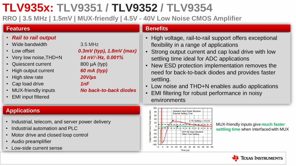
TLV935x: TLV9351 / TLV9352 / TLV9354 RRO | 3.5 MHz | 1.5mV | MUX-friendly | 4.5V - 40V Low Noise CMOS Amplifier
• Industrial, telecom, and server power delivery
• Industrial automation and PLC
• Motor drive and closed loop control
• Audio preamplifier
• Low-side current sense
Features Benefits
Applications
• High voltage, rail-to-rail support offers exceptional
flexibility in a range of applications
• Strong output current and cap load drive with low
settling time ideal for ADC applications
• New ESD protection implementation removes the
need for back-to-back diodes and provides faster
settling.
• Low noise and THD+N enables audio applications
• EMI filtering for robust performance in noisy
environments
• Rail to rail output
• Wide bandwidth 3.5 MHz
• Low offset 0.3mV (typ), 1.8mV (max)
• Very low noise,THD+N 14 nV/√Hz, 0.001%
• Quiescent current 800 µA (typ)
• High output current 60 mA (typ)
• High slew rate 20V/µs
• Cap load drive 1nF
• MUX-friendly inputs No back-to-back diodes
• EMI input filtered
MUX-friendly inputs give much faster
settling time when interfaced with MUX

Standard Amplifier Roadmap Sampling Production
LM2904 | LM2902
32V, 0.7MHz, 7mV, 0 to +70C 26V, 7mV, -40 to +125°C
LM2904LV | LM2902LV 5.5V, 3mV, -40 to +125°C
Sta
nd
ard
Am
plifi
ers
TL07x | TL08x
32V, 0.7MHz, 7mV, 0 to +70C 30V, 3MHz, 10mV, -40 to +85°C
TL06x
32V, 0.7MHz, 7mV, 0 to +70C 36V, 1MHz, 6mV, -40 to +85°C
TL07xH | TL08xH 36V, 4MHz, 4mV, -40 to +125°C
TL06xH 36V, 1MHz, 4mV, -40 to +125°C
LM358 | LM324
32V, 0.7MHz, 7mV, 0 to +70C 32V, 7mV, 0 to +70°C
LM358LV | LM324LV 5.5V, 3mV, -40 to +125°C
LM2904B 36V, 3mV, -40 to +125°C
LM358B 36V, 3mV, -40 to +85°C

Specs LM358 LM358A LM2904 LM358B LM2904B LM358LV
LM2904LV
Supply Voltage 3V to 32V 3V to 32V 3V to 26V 3V to 36V 3V to 36V 2.7V to 5.5V
Temp. Range 0° to 70°C 0° to 70°C -40° to 125°C -40° to 85°C -40° to 125°C -40° to 125°C
VOS (max) 7 mV 3 mV 7 mV 3 mV 3 mV 3 mV
IB (typ) 20 nA 15 nA 20 nA 10 nA 10 nA 15 pA
GBW 0.7 MHz 0.7 MHz 0.7 MHz 1.2 MHz 1.2 MHz 1 MHz
Slew Rate 0.3 V/µs 0.3 V/µs 0.3 V/µs 0.5 V/µs 0.5 V/µs 1.5 V/µs
IQ (typ) 350 µA 350 µA 350 µA 300 µA 300 µA 90 µA
ESD Rating (HBM) 500V 500V 500V 2kV 2kV 2kV
Other Features – – – EMI Hardened EMI Hardened EMI Hardened
Packages SOIC, TSSOP,
VSSOP, PDIP
SOIC, TSSOP,
VSSOP, PDIP
SOIC, TSSOP,
VSSOP, PDIP
SOIC, TSSOP, VSSOP,
SOT-23-8, WSON
SOIC, TSSOP, VSSOP,
SOT-23-8, WSON
SOIC, TSSOP, VSSOP,
SOT-23-8, WSON
LM358B -40° to 85°C
LM2904B -40° to 125°C
LM358LV -40° to 125°C
LM2904LV -40° to 125°C
Up to 36V
≤5.5V
LM358 0° to 70°C
LM258 -25° to 85°C
LM2904 -40° to 125°C
Legacy Portfolio New Portfolio
New Standard Amplifiers | LM358 & LM2904 refresh
L
M3xx
| L
M290
x Fa
mily
Com
pari
sons
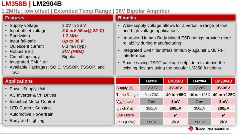
LM358B | LM2904B 1.2MHz | low offset | Extended Temp Range | 36V Bipolar Amplifier
• Power Supply Units
• AC Inverter & VF Drives
• Industrial Motor Control
• LED Current Sensing
• Automotive Powertrain
• Body and Lighting
• Wide supply voltage allows for a versatile range of low
and high voltage applications
• Improved Human Body Model ESD ratings provide more
reliability during manufacturing
• Integrated EMI filter offers immunity against EMI/ RFI
interference
• Space saving TSOT package helps to miniaturize the
existing designs using the popular LM358 functions
• Supply voltage 3.0V to 36 V
• Input offset voltage 3.0 mV (Max@ 25ᵒC)
• Bandwidth 1.2 MHz
• Input fail-safe Up to 36 V
• Quiescent current 0.3 mA (typ)
• Robust ESD 2kV (HBM)
• Circuit topology Bipolar
• Integrated EMI filter
• Available Packages: SOIC, VSSOP, TSSOP, and
TSOT
LM358 LM358B LM2904 LM2904B
Supply (V) 3V-32V 3V-36V 3V-26V 3V-36V
Temp Range 0 to 70C -40 to +85C -40 to +125C -40 to +125C
VOS (max) 7mV 3mV 7mV 3mV
IQ / ch (typ) 350µA 300µA 350µA 300µA
EMI Filters ✔ ✔
ESD (HBM) 500V 2kV 500V 2kV
Features Benefits
Applications

LM358BA | LM2904BA 1.2MHz | Low offset | Extended Temp Range | 36V Bipolar Amplifier
• Wide supply voltage allows for a versatile range of low
and high voltage applications
• Improved Human Body Model ESD ratings provide more
reliability during manufacturing
• Integrated EMI filter offers immunity against EMI/ RFI
interference
• Space saving TSOT package helps to miniaturize the
existing designs using the popular LM358 functions
• Supply voltage 3.0V to 36 V
• Input offset voltage 1.75 mV (Max@ 25ᵒC)
• Bandwidth 1.2 MHz
• Input fail-safe Up to 36 V
• Quiescent current 0.3 mA (typ)
• Robust ESD 2kV (HBM)
• Circuit topology Bipolar
• Integrated EMI filter
• Available Packages: SOIC, VSSOP, TSSOP, and
TSOT
Features Benefits
Applications
• Power Supply Units
• AC Inverter & VF Drives
• Industrial Motor Control
• LED Current Sensing
• Automotive Powertrain
• Body and Lighting
LM358A LM358BA LM2904A LM2904BA
Supply (V) 3V-32V 3V-36V 3V-26V 3V-36V
Temp Range 0 to 70C -40 to +85C -40 to +125C -40 to +125C
VOS (max) 3mV 1.75mV 3mV 1.75mV
IQ / ch (typ) 350µA 300µA 350µA 300µA
EMI Filters ✔ ✔
ESD (HBM) 500V 2kV 500V 2kV
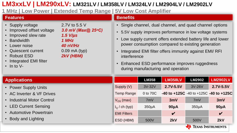
LM3xxLV | LM290xLV: LM321LV / LM358LV / LM324LV / LM2904LV / LM2902LV
1 MHz | Low Power | Extended Temp Range | 5V Low Cost Amplifier
• Power Supply Units
• AC Inverter & VF Drives
• Industrial Motor Control
• LED Current Sensing
• Automotive Powertrain
• Body and Lighting
• Single channel, dual channel, and quad channel options
• 5.5V supply improves performance in low voltage systems
• Low supply current offers extended battery life and lower
power consumption compared to existing generation
• Integrated EMI filter offers immunity against EMI/ RFI
interference
• Enhanced ESD performance improves ruggedness
during manufacturing and operation
• Supply voltage 2.7V to 5.5 V
• Improved offset voltage 3.0 mV (Max@ 25ᵒC)
• Improved slew rate 1.5 V/µs
• Bandwidth 1 MHz
• Lower noise 40 nV/Hz
• Quiescent current 0.09 mA (typ)
• Robust ESD 2kV (HBM)
• Integrated EMI filter
• In to V-
Features Benefits
Applications LM358 LM358LV LM2902 LM2902LV
Supply (V) 3V-32V 2.7V-5.5V 3V-26V 2.7V-5.5V
Temp Range 0 to 70C -40 to +125C -40 to +125C -40 to +125C
VOS (max) 7mV 3mV 7mV 3mV
IQ / ch (typ) 350µA 90µA 350µA 90µA
EMI Filters ✔ ✔
ESD (HBM) 500V 2kV 500V 2kV

New Standard Amplifiers | TL06x, TL07x, TL08x refresh
Part GBW
TL06x 1 MHz
TL07x 3 MHz
TL08x 3 MHz
X = 1, 2, and 4 (channel count)
Part GBW
TL06xH 1 MHz
TL07xH 4 MHz
TL08xH 4 MHz
Legacy Portfolio New Portfolio
Specs TL06x TL06xH TL07x TL07xH TL08x TL08xH
RTM Existing 2Q20 Existing 2Q20 Existing 2Q20
Supply Voltage 7V – 36V 4.5V - 36V 7V – 36V 4.5V - 36V 10V – 30V 4.5V - 36V
VOS (max) 15mV 4mV 6 mV 4mV 15mV (C grade)
6mV (I grade) 4mV
IB (typ) 30 pA 5 pA 65 pA 30 pA 30 pA 30 pA
GBW 1 MHz 1MHz 3 MHz 4 MHz 3 MHz 4 MHz
Slew Rate 3.5 V/us 3.5 V/us 13 V/us 20 V/us 13 V/us 20 V/us
IQ (typ) 0.2 mA/ch 0.1 mA/ch 1.4 mA/ch 0.8 mA/ch 1.4 mA/ch 0.8 mA/ch
ESD 2kV ESD 2kV ESD 2kV ESD 2kV ESD 1kV ESD 2kV ESD
Temp Grades 0 – 70C (C),
-40 to 85C (I) -40 – 125C
0 – 70C (C),
-40 to 85C (I) -40 – 125C
0 – 70C (C),
-40 to 85C (I) -40 – 125C

TL06xH: TL061H / TL062H / TL064H RRI to V+ | 1MHz | 4mV | 4.5V – 36V General Purpose Amplifier
• Industrial automation and PLC
• Motor drive and closed loop control
• Audio preamplifier and DAC buffer
• High-side current sense
Features Benefits
Applications
• High voltage support offers robust flexibility in a range
of industrial applications
• Low offset and drift offer improved accuracy
• Input common mode range to V+ enables high side
current sensing applications
• High slew rate for motor control and closed loop
control applications
• EMI filtering for robust performance in noisy
environments
• Wide Supply Range 4.5V – 36V
• Wide Bandwidth 1 MHz
• Low Offset 2mV/4mV (typ/max)
• Low offset drift 3µV/°C
• Low Noise 37 nV/√Hz
• Quiescent Current 100µA (typ)
• High Slew Rate 3.5V/µs
• ESD 2kV HBM
• Full industrial temp range -40 to 125°C
• Integrated EMI filter
TL072C

TL07xH: TL071H / TL072H / TL074H RRI to V+ | 4MHz | 2mV | 4.5V – 36V Low Noise General Purpose Amplifier
• Industrial automation and PLC
• Motor drive and closed loop control
• Audio preamplifier and DAC buffer
• High-side current sense
Features Benefits
Applications
• High voltage support offers robust flexibility in a range
of industrial applications
• Low offset and drift offer improved accuracy
• Input common mode range to V+ enables high side
current sensing applications
• Low noise and THD+N enables audio applications
• High slew rate for motor control and closed loop
control applications
• EMI filtering for robust performance in noisy
environments
• Wide Supply Range 4.5V – 36V
• Wide Bandwidth 4 MHz
• Low Offset 2mV/4mV (typ/max)
• Low offset drift 3µV/°C
• Very Low Noise, THD+N 18 nV/√Hz, 0.003%
• Quiescent Current 1mA (typ)
• High Slew Rate 13V/µs
• ESD 2kV HBM
• Full industrial temp range -40 to 125°C
• Integrated EMI filter
TL072C

TL08xH: TL081H / TL082H / TL084H RRI to V+ | 4MHz | 2mV | 4.5V – 36V General Purpose Amplifier
• Industrial automation and PLC
• Motor drive and closed loop control
• Audio preamplifier and DAC buffer
• High-side current sense
Features Benefits
Applications
• High voltage support offers robust flexibility in a range
of industrial applications
• Low offset and drift offer improved accuracy
• Input common mode range to V+ enables high side
current sensing applications
• High slew rate for motor control and closed loop
control applications
• EMI filtering for robust performance in noisy
environments
• Wide Supply Range 4.5V – 36V
• Wide Bandwidth 4 MHz
• Low Offset 2mV/4mV (typ/max)
• Low offset drift 3µV/°C
• Quiescent Current 1mA (typ)
• High Slew Rate 13V/µs
• ESD 2kV HBM
• Full industrial temp range -40 to 125°C
• Integrated EMI filter
TL072C

PSpice for TI Introduction and Demo
New Product Update webinar series
Jerry Madalvanos
36

Agenda
• Benefits of PSpice for TI
• How to Download
• Creating and running a project
– Live demo
37

Benefits of PSpice® for TI – Free Version • PSpice for TI is a new design and simulation tool that utilizes
the industry leading Cadence® PSpice technology
• Familiar Cadence® environment (industry’s most widely used
schematic capture and simulation environment).
• Full-featured simulator
– Automatic measurements, post-processing, advanced analyses
(Monte Carlo, Worst-case, Thermal)
• Training Videos: Introduction and Advanced
• Integration with TI.com
– Integrated library with thousands of built-in models that
automatically synchronizes with TI.com
– E2E Forum Support
– Ability to work off-line
• Simulate with unlimited markers for TI models
– 3 marker limit for non-TI models, paid upgrade unlocks marker limit
38

Helpful Resources
• Download Link
– https://www.ti.com/tool/PSPICE-FOR-TI
• Tutorial Videos
– https://training.ti.com/pspice-ti-introduction
39

Downloading PSpice® for TI
• Navigate to https://www.ti.com/tool/PSPICE-FOR-TI
• Click “Request”
• Login to your myTI account and fill out
the required information
• Approval can be immediate
– May take 24-48 hours (excluding weekends)
• Follow the instructions in the email to
download PSPICE for TI
40
Live Demo
• How to create a project
• How to build a simple circuit (op amp, passives, sources, label nets)
• How to create & run a simulation profile (transient)
• How to view the results
• How to export the design as a *.zip file
41

Creating Project
• In the toolbar go to File New Project
42

Creating Project
• Name the project
• Choose the file location for the project
– Click OK
• Select “Create a Blank Project”
– Click OK
43

Circuit Template
• This step-by-step guide uses the
inverting summer circuit outlined in the
Analog Engineer’s Circuit
Cookbook (Page 18)
44

Placing the Op Amp
• Navigate to the right hand toolbar
labeled “PSpice Part Search”
• Type “TLV170” into the search
box, and click the magnifying
glass icon – Alternatively, you can navigate the folders
above the search bar and find it in Texas
Instruments/Amplifiers/Operational
Amplifiers/General Purpose Op
Amps/TLV170
• Double-click “TLV170”
mouse over the schematic
click and place the op amp
– Press ESC to stop placing
TLV170 45
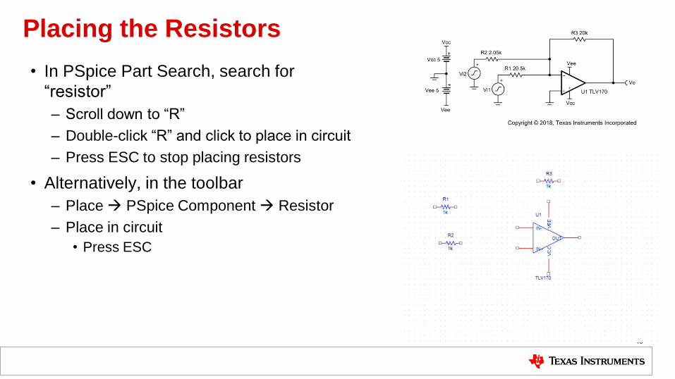
Placing the Resistors
• In PSpice Part Search, search for
“resistor”
– Scroll down to “R”
– Double-click “R” and click to place in circuit
– Press ESC to stop placing resistors
• Alternatively, in the toolbar
– Place PSpice Component Resistor
– Place in circuit
• Press ESC
46
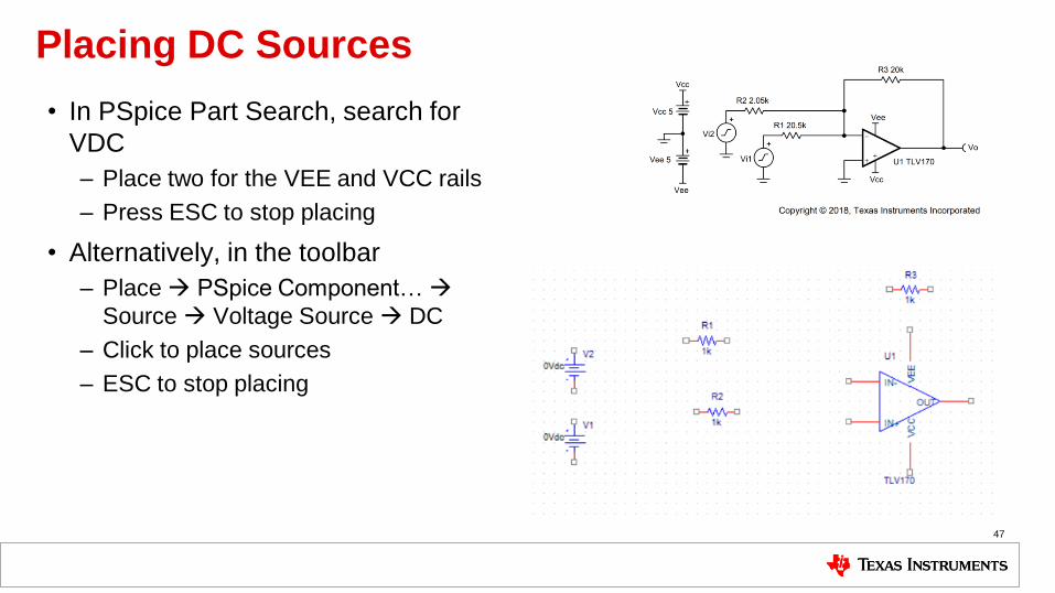
Placing DC Sources
• In PSpice Part Search, search for
VDC
– Place two for the VEE and VCC rails
– Press ESC to stop placing
• Alternatively, in the toolbar
– Place PSpice Component…
Source Voltage Source DC
– Click to place sources
– ESC to stop placing
47

Placing Input Sources
• In PSpice Part Search, search for
VDC
– Place two for the Vin1 and Vin2
– Press ESC to stop placing
• Alternatively, in the toolbar
– Place PSpice Component…
Source Voltage Sources Sine
– Click to place sources
– ESC to stop placing
48

Placing Grounds
• Press “g” to start the “Place
Ground tool
• Choose “0/CAPSYM” and place
grounds in circuit
– Press OK
– Place in Circuit
– Press ESC
• Alternatively
– Navigate to the toolbar
and click “Place”, select “Ground…”
49

Wiring the Circuit
• Press “w” to start the wiring tool
– Alternatively, in the toolbar:
• Place Wire
• Press ESC to exit the wiring tool
• Connect components based on
the inverting summer circuit
• Note: Place wires on V1, V2, and
U1 as shown to attach net labels
to them
50

Labeling Nets
• Press “n” to open the “Place
Net Alias” tool
– Alternatively, in the toolbar:
• Place Net Alias…
• Enter the name of the net
and click a wire to place the
label
– For this example, place the
following nets:
• Vcc
• Vee
• Vin1
• Vin2
• Vout
51

Assigning Values to Components
• Double-click the value you wish
to edit (not the component)
• Enter the value based upon the inverting
summer circuit from the Analog Engineer’s
Cookbook
• Repeat process until all values
match the cookbook circuit
52

Analyzing the Circuit
• In the toolbar, click the
“New Simulation Profile” button
• Enter a name for your simulation
• Press “Create”
• Edit the “Run To Time” to 3ms
– This will show 3 periods of the
longest waveform
• Press “OK”
53

Running the Simulation
• In the toolbar, click the
“Voltage/Level Marker”
button
• Place Voltage markers
on Vout, Vin1, and Vin2
• Press the “Run PSpice”
button
• Open the PSpice
simulation window
• Note: The first simulation may
take several minutes…
54

Viewing the Results
• To split traces, right click
the plot and select “Add
Plot”
• Repeat the above step so
there are three plots total
• Click the name of the trace
in the bottom left corner
• Cut the trace and paste
one on each plot
55

Comparing Simulation to Cookbook Results
• Simulation matches the
expected output!
56

Exporting Project
• Back in the PSpice for TI window
• Click on the .dsn file in the project directory
• In the toolbar, navigate to “File” then to
“Archive Project”
• Make sure “Library files”, “Include
TestBench”,“Referenced projects”, and
“Create single archive file” are selected
• Select the archive directory and name the
file, then hit “OK”
• The zipped project can easily be sent for
analysis
57

Helpful Notes
• If PSpice part search is not open by default, you can
open it by navigating to “Place”, “PSpice Component”,
“Search…”
58

59
Visit www.ti.com/npu
For more information on the New Product Update
series, calendar and archived recordings

60

IMPORTANT NOTICE AND DISCLAIMER
TI PROVIDES TECHNICAL AND RELIABILITY DATA (INCLUDING DATASHEETS), DESIGN RESOURCES (INCLUDING REFERENCE DESIGNS), APPLICATION OR OTHER DESIGN ADVICE, WEB TOOLS, SAFETY INFORMATION, AND OTHER RESOURCES “AS IS” AND WITH ALL FAULTS, AND DISCLAIMS ALL WARRANTIES, EXPRESS AND IMPLIED, INCLUDING WITHOUT LIMITATION ANY IMPLIED WARRANTIES OF MERCHANTABILITY, FITNESS FOR A PARTICULAR PURPOSE OR NON-INFRINGEMENT OF THIRD PARTY INTELLECTUAL PROPERTY RIGHTS.These resources are intended for skilled developers designing with TI products. You are solely responsible for (1) selecting the appropriate TI products for your application, (2) designing, validating and testing your application, and (3) ensuring your application meets applicable standards, and any other safety, security, or other requirements. These resources are subject to change without notice. TI grants you permission to use these resources only for development of an application that uses the TI products described in the resource. Other reproduction and display of these resources is prohibited. No license is granted to any other TI intellectual property right or to any third party intellectual property right. TI disclaims responsibility for, and you will fully indemnify TI and its representatives against, any claims, damages, costs, losses, and liabilities arising out of your use of these resources.TI’s products are provided subject to TI’s Terms of Sale (www.ti.com/legal/termsofsale.html) or other applicable terms available either on ti.com or provided in conjunction with such TI products. TI’s provision of these resources does not expand or otherwise alter TI’s applicable warranties or warranty disclaimers for TI products.
Mailing Address: Texas Instruments, Post Office Box 655303, Dallas, Texas 75265Copyright © 2020, Texas Instruments Incorporated