New designs of reversible sequential devices - arXiv
14
kTln2 k =1.3806505 × 10 -23 m 2 kg 2 K -1 (JoulesKelvin -1 ) arXiv:0908.1620v1 [quant-ph] 12 Aug 2009
-
Upload
khangminh22 -
Category
Documents
-
view
0 -
download
0
Transcript of New designs of reversible sequential devices - arXiv

New designs of reversible sequential devices
Anindita Banerjee and Anirban Pathak
October 30, 2018
Jaypee Institute of Information Technology University, Noida, India
Abstract
A clear protocol for synthesis of sequential reversible circuits from any particular gate library has beenprovided. Using that protocol, reversible circuits for SR latch, D latch, JK latch and T latch are designed fromNCT gate library. All the circuits have been optimized with the help of existing local optimization algorithms(e.g. template matching, moving rule and deletion rule). It has been shown that the present proposals havelower gate complexities, lower number of garbage bits, lower quantum cost and lower number of feedback loopscompared to the earlier proposals. For a fair comparison, the optimized sequential circuits have been comparedwith the earlier proposals for the same after converting the earlier proposed circuits into equivalent NCT circuits.Further, we have shown that the advantage in gate count obtained in some of the earlier proposals by introductionof New gates is an artifact and if it is allowed then every reversible circuit block can be reduced to a single gate. Inthis context, some important conceptual issues related to the designing and optimization of sequential reversiblecircuits have been addressed. A protocol for minimization of quantum cost of reversible circuit has also beenproposed here.
1 Introduction
Landauer's principle [1] states that any logically irreversible operation on information, such as the erasure of a bitor the merging of two computation paths, is always associated with an increase of entropy of the non-informationbearing degrees of freedom of the information processing apparatus or its environment. Each bit of lost informationwill lead to the release of at least kT ln2 amount of heat, where k = 1.3806505×10⁻²³m2kg2K−1(JoulesKelvin−1)is Boltzamann's constant and T is the absolute temperature at which the operation is performed. By 2020 this losswill become a substantial part of energy dissipation in VLSI circuits, if Moore's law continues to be in e�ect. Thisparticular problem of VLSI designing was realized by Feynman and Bennet in 1970s. In 1973 Bennet [2] had shownthat energy dissipation problem of VLSI circuits can be circumvented by using reversible logic. This is so becausereversible computation does not require to erase any bit of information and consequently it does not dissipate anyenergy for computation. Reversible computation requires reversible logic circuits and synthesis of reversible logiccircuits di�ers signi�cantly from its irreversible counter part because of di�erent factors [3]. The technologicalrequirement of designing of energy dissipation free VLSI circuits, particular characteristics of synthesis and testingof reversible circuits and the tremendous advantage of quantum circuits have motivated scientists and engineersfrom various background (eg. Physics, Electronics, Computer science, Mathematics, Material science, Chemistry)to study various aspects of reversible circuits.
Quantum mechanical operations are always reversible and consequently all quantum gates are reversible. Aclassical reversible gate can not handle superposition of states (qubit) so it forms a special case of quantum circuit ora subset of the set of the quantum circuits. But from the construction point of view classical reversible gates are easyto build [4, 5]. A lot of interesting works have already been reported in the �eld of synthesis [6]-[10], optimization[11, 12], evaluation [13] and testing [14] of reversible circuits. In a short period the reversible computation hasemerged as a promising technology having applications in low power CMOS [15], nanotechnology [16], opticalcomputing [17], optical information processing, DNA computing [18], bioinformatics, digital signal processing andquantum computing [3]. From these wide range of potential applications and from the energy dissipation problemof VLSI it is clearly evident that the reversibility will play dominant role in designing circuits in future.
But the designing aspect of reversible sequential circuit is not yet studied rigorously. This is because of thefact that feedback in a reversible circuit can not be visualized in the usual sense in which feedback is visualizedin a conventional irreversible circuit. This issue was �rst addressed by To�oli [19], where he had shown that thereversible sequential circuits can be constructed provided the transition function of the circuit block without thefeedback loop is unitary. His ideas on the sequential reversible circuit had further strengthen in his pioneering workon conservative logic [20]. Later on some e�orts have been made to construct reversible sequential circuit [21]-[28].All these e�orts are concentrated on the designing of various �ip �ops because of the fact that the �ip �ops are thebasic building block of the memory element of a computer and if one wishes to build a reversible classical computerthen these designs will play a crucial role. But several conceptual issues related to designing and optimization
1
arX
iv:0
908.
1620
v1 [
quan
t-ph
] 1
2 A
ug 2
009

Figure 1: Reversible gate
Table 1: And gate; a. Irreversible and b. Reversible
of reversible sequential circuits are not addressed till now. The earlier works [21]-[28] neither provide any clearprotocol for synthesis of reversible sequential circuit nor they have systematically tried to think beyond the scope ofclassical irreversible logic. Further the quantum cost of the reversible sequential elements have not been calculatedso far nor a systematic algorithm for minimization of quantum cost has been reported. These facts have motivatedus to provide a protocol for synthesis of optimized reversible circuits. We have also provided a protocol to optimizethe quantum cost of a reversible circuit/gate. We have also addressed the other important conceptual issues relatedto the designing of reversible sequential circuits. In the next section we provide background of reversible circuitsand in section 3 we address conceptual issues related to the feedback and the choice of gate library. In section 4 wehave discussed the earlier approaches and their limitations. In section 5, we have provided a protocol for synthesisof reversible circuits we have also used it to design reversible sequential elements. In section 6, we have given aprotocol for comparing our designs with the earlier proposals. Finally we conclude in section 7.
2 Background
A reversible logic circuit comprises of reversible gates. A gate is reversible if it has equal number of inputs andoutputs and the boolean function that maps the input in output is bijective. Consider Fig. 1, where input vector Iis (x1, x2, ......xn) and output vector O is (y1, y2, ......yn). The gate (function) is reversible if it satis�es the conditionof one to one and onto mapping between input and output domains.
A garbage bit is the additional output to make a function reversible and it is not used for further computations.Therefore large number of garbage bits are undesirable in a reversible circuit. As an example, in Table 1 we haveshown an irreversible and a reversible AND gate. It is evident that the Z output gives us the required output andthe other outputs X and Y are garbage.
The quantum cost [13, 29, 30, 31] of a reversible gate is the number of primitive quantum gates needed toimplement the gate. All (1× 1) and (2× 2) are considered as quantum primitive gate and the cost all quantumprimitive gates are considered. For example we can construct To�oli with square root of not gate (V) and CNOTand in that construction the total gate count of To�oli is �ve [32]. Thus the quantum cost of To�oli is �ve.
Following two methods have been provided by Mohammadi [33] to �nd the quantum cost of a non-primitivereversible gate or a circuit:
1. Implement a circuit/gate using only the quantum primitive (1× 1) and (2× 2) gates and count them [29, 30,33].
2. Synthesize the new circuit/gate using the well known gates whose quantum cost is speci�ed and add up theirquantum cost to calculate total quantum cost [33, 34].
At this point we would like to mention that quantum cost obtained in these two procedures may be higher thanthe actual one unless local optimization algorithm is applied to equivalent circuit obtained in terms of quantumprimitive gates. Further we would like to mention that there is a conceptual di�erence between optimizationalgorithm used for reduction of circuit complexity and the one used for reduction of quantum cost. This is sobecause in case of circuit optimization we are restricted to a gate library but to reduce the quantum cost we canintroduce any New gate as long as the gate is (1× 1) or (2× 2). Let us show how the modi�ed local optimization
2

Figure 2: Modi�ed local optimization algorithm (moving rule) is applied to minimize the quantum cost of Fredkingate
Figure 3: Protocol for optimization of quantum cost
algorithm may help. Consider a Fredkin gate as given in Fig 2a. which has 3 To�oli gates. This can further bereduced by template matching to one To�oli and two CNOT gates as shown in Fig. 2b. If we substitute the To�oligates by quantum primitives we obtain the circuit shown in Fig. 2c. According to Mohammadi's methods [33] thequantum cost is seven. We now apply the moving rule [11] twice to circuit in Fig 2c (the movements are shown byarrows) to obtain Fig. 2d, in which the quantum cost of Fredkin gate is found to be �ve. Here we would like to drawyour attention towards the fact that the moving rule (which was essentially designed to reduce circuit complexity)has not reduced the circuit complexity but it has reduced the quantum cost.
Thus we have established that local optimization play a very crucial role in reducing the quantum cost, earlierworks [13, 33, 34] have not provided adequate attention towards this fact and consequently we observe that quan-tum cost of several gates proposed in earlier works on reversible circuits can be reduced using local optimizationalgorithms. Here we would like to note that the recently Maslov [12] has used local optimization technique basedon templates to reduce the quantum circuit cost but he has not provided any systematic protocol for reduction ofquantum cost.
We have shown our protocol in Fig. 3 and have used it to �nd quantum cost of our circuit and also the quantumcost of di�erent reversible circuits proposed in [29, 33, 34].
3

3 Conceptual issues related to reversible circuit
To provide a systematic protocol for designing reversible sequential circuit and to compare the proposed circuitdesigns with the existing designs we need to address certain conceptual issues related to reversible circuit designing.To be precise, conceptual issues related to feedback, choices of gate library and approximate optimization (localoptimization) techniques will be addressed in the following subsections.
3.1 Feedback in a reversible circuit
Figure 4: Circuit a and b are equivalent but the idea of time axis is not valid in b. Here |Ψ(t)〉 is the product stateat time t and t3 > t2 > t1 > 0
.
It is widely believed that feedback is not allowed in a reversible circuit. This is true if we consider feedback in asimilar fashion as it is dealt in classical irreversible logic. The objection against feedback is twofold. Firstly, mergingof two computational paths is not allowed in a reversible circuit and secondly, time axis goes from left to right ina reversible circuit (as shown in Fig. 4a). Thus if we need to follow the same notion of time axis in a reversiblesequential circuit then feedback will essentially mean a journey in negative time axis or existence of time machine.This is against the notion of physical reality. But these strong objections against feedback in reversible circuit canbe circumvented by establishing the equivalence between the circuits in Fig. 4a and Fig. 4b. To be precise, thefeedback loop shown in Fig. 4b is only in space not in time. Therefore, the circuit in Fig. 4b is equivalent to acascaded circuit in time axis (see Fig. 4a). Thus the usual notion of time axis is not valid in reversible sequentialcircuit (i.e. in a circuit having spatial feedback loop similar to one shown in Fig. 4b). Further, since the circuit inFig. 4b is equivalent to the cascade shown in Fig 4a, there is no merging of computational paths and consequentlythere would not be any loss of energy provided U is unitary. This conclusion coincides with the To�oli's idea [19]of unitary transition function. Now if we follow, this notion of feedback, then to establish the reversibility of thedesign it would be su�cient to establish the unitarity of U. Here we would also like to note that in this restrictednotion of spatial feedback we can not allow any arbitrary feedback loop. An allowed loop has to be reducible to thestructure shown in Fig. 4b.
3.2 Latch and Flip �op
In digital designing a latch is de�ned as a bistable memory unit which changes its output with the input and isindependent of a clock. The term �ip �op is de�ned as a sequential device that samples its input and changes itsoutput only at times determined by clock signals. But this is also called gated latch in some books [35, 36]. Inthese books �ip �op are constructed from two gated latches, one of them is the master latch and other is the slavelatch. They have classi�ed �ip �ops into two categories one is master slave �ip �op. In this �ip �op the masterlatch is disabled when (clock pulse) CP=0 and slave latch is disabled when CP=1. The other type of �ip �op isedge triggered �ip �op and this synchronizes the state changes during a CP transition. The structure of masterslave type and edge triggered type are same that is it consists of two gated latches with a not gate as shown in Fig7b. This methodology has been followed throughout the existing designs for [22, 28]. Hence for reversible sequentialcircuit designing, it is important to mention which convention is used but hardly any previous works has mentionedthis.
3.3 Gate library: Which gates should be used for the synthesis of the reversible
circuit?
Whichever synthesis algorithm we follow, it is important to chose a gate library which is universal but the choiceof the gate library (i.e. gates which are the member of that library) is not unique and there does not exist any
4

Table 2: Reversible gates from NCT gate library, their size and functions.
single convention. The physical complexity of gates may not be same in two di�erent implementation of reversiblecircuits. For example, it may be easy to build an arbitrary gate 'A' in MOSFET technology but it may not be thateasy to implement in optical based technology [37, 38]. A N-qubit reversible gate is represented by 2Nx 2N unitarymatrix and product of any arbitrary number of unitary matrices is always unitary. Consequently, if we put a setof reversible quantum gates in a black box then an unitary matrix will represent the box and one can technicallyconsider it as a New gate. If we allow such construction of New gates then any circuit block (of arbitrary size) canbe reduced to a single New gate. 1
Thus it is straightforward to observe that the use of New gate to reduce the gate count [39]-[43] is an artifact.To be precise, we would like to mention that to reduce the gate complexity and garbage bits various papers havereported di�erent New gates. For example, Hassan Babu [40] has introduced a 3x3 New gate for full adder circuit,H. Thapliyal [24, 39] has introduced New gate and 3x3 TKS gate for multiplexer based full adder and multipliersand a 4x4 TSG gate for carry look-ahead and other adder architectures. In [26] he has also introduced New To�oligate and New Fredkin gate for SR latch and JK Gated latch respectively. Majid Haghparast [41]-[43] has proposedvarious gates, which includes New Fault Tolerant gate for fault tolerant reversible logic circuits, HNG gate forreversible multiplier circuit and MKG gate for full adder. Thus the gate count (gate complexity) reported in theseworks are misleading and consequently we need a logical approach to construct an universal gate library which inturn will help us to compare more than one circuit designs proposed for the same purpose.
Figure 5: Realization of classical irreversible operations with the help of reversible gates: a) COPY gate, b) ANDgate, c) NAND gate, d) OR gate, e) NOR gate
Di�erent universal set of quantum gates have been reported by various groups and among them one of partic-ular interest was introduced by Aharonov [44] which contains Hadamard (H) and To�oli (T) gates. Thus for allcomputation in the domain of classical reversible computation it is su�cient to consider To�oli as the universalgate. This is easy to visualize through Fig. 5c where it is shown that the NAND gate can be constructed usingTo�oli. Further we would like to note that NOT and CNOT gates can be achieved from (T) gates. (For NOT gatechoose both the �rst and second control bits as |1〉 and for CNOT gate choose the �rst control bit as |1〉.) To�oli[19] had also shown that the NCT gate library is universal for the synthesis of reversible Boolean circuits. Actuallythe inclusion of NOT and CNOT makes the universal set over complete but this inclusion is justi�able from theperspective of implementational simplicity [4, 5, 38] and consistency with earlier works [7, 29].
Maslov has prescribed a reversible logic synthesis benchmark [29] in which he has suggested several gate libraries,which are NCT (NOT, CNOT, To�oli), NCTSF ( NOT, CNOT, To�oli, Swap, Fredkin), GT (generalized n-bitTo�oli) and GT&GF (generalized To�oli and generalized n-bit Fredkin). Among these libraries NCT library is thesmallest complete set. Consequently NCT is a good choice of gate library. Further, these gates can be experimentallyrealized using MOSFET [4, 5] and simple optics [37, 38]. Keeping all these facts in mind, we have chosen NCT gatelibrary. The circuits from NCT gate library as shown in Table 2 is called NCT circuits. In text we will refer NOT asN, CNOT as C, To�oli as T. In addition to NCT circuits of reversible sequential elements we have also synthesizedNCV circuits for the same. The NCV circuits are made using gates from NCV gate library, which includes N, C,controlled V and controlled V + gates, is complete. In [3] the universality of this library is proved and this libraryis also used in earlier work [12]. Further the NCV circuits are required for determination of quantum cost. Here we
1This is true in case of any quantum circuit block too, provided it does not contain any measurement operation.
5

would like to note that the quantum cost of circuit is the number of quantum primitive gates required to constructthe circuit. Since T is not a quantum primitive gate, an NCT circuit can not be used directly to determine thequantum cost. But T can be constructed using square root of not gate (V) and CNOT and in that construction thetotal gate count of To�oli is �ve [30, 32]. It is also interesting to note that according to the Solovay-Kitaev theorem[45] translation between di�erent universal sets causes only poly-logarithmic overhead. We have used these facts tocompare our designs of sequential circuits with the existing proposals. The comparison is done with respect to theNCT gate library, NCV gate library, number of garbage bits (G), quantum cost (QC) and total cost (TC)2 which isas shown in Table 3, 4 and 5. It should be noted that reversible logic is used in many areas like optical computing,low power CMOS design, DNA computing quantum computing etc. The choice of gate library has a signi�cant rolein designing implementable feasibility and resources cost.
3.4 Why are the optimized designs di�erent?
Even if we start with the same truth table and same gate library then also di�erent logical paths may lead to di�erentcircuits. After designing a circuit we need to optimize it but an exact optimization technique's time complexity (τ)is
τ = O(22nnlm
)(1)
where, n is the number of qubit line present in the circuit, m is the total number gate present in the circuit and lis the number of qubit associated with the largest gate present in the gate library where l ≤ n. Thus in the presentcase when the gate library is (NCT) then l = 3 and the time complexity of global optimization algorithm is
τ = O(22nn3m
)(2)
This increases exponentially with n and m. In order to avoid this exponential rise in time, certain approximateoptimization (local optimization) algorithms [11, 12] have been designed and in practice we use them. Sincethe optimization algorithm is an approximate one, it may lead to di�erent circuit designs but the order of gatecomplexities have to be the same. This fact is clearly re�ected in the Table 3, 4 and 5 given below.
4 How to design the circuit
4.1 Earlier approaches
In the previous subsection we have shown that in order to design a reversible sequential circuit we have to designU as in Fig. 4, as unitary. Now if we know the truth table of U and wish to decompose U in terms of �nite numberof logic gates, we can use one of the two existing approaches.
1. The �rst approach is the direct substitution method where one designs reversible circuit [21] - [26] by substi-tuting the irreversible gates with equivalent reversible gates. To understand this let us take an example, seeFig 2. in which the classical irreversible gates like OR, NOR, AND, NAND, etc are replaced by correspondingNCT reversible gates (Fig 2b and 2c) and NCT reversible circuits (Fig 2d and 2e) respectively. In this ap-proach after designing the equivalent gates one can substitute each irreversible gate of a conventional circuitby corresponding equivalent reversible gates and obtain the required reversible circuit. The application ofthis approach is limited since it requires an existing reversible circuit and it can not go beyond the limits ofclassical computation. Picton [21] has substituted Fredkin gates in the traditional SR latch built from NORgates, Rice [22, 23] has used To�oli gate in SR latch and used Fredkin gate to generate fanout from the clock.Thapliyal [24] has substituted NAND gate by a New gate and AND gate by Fredkin gate. In another paperof Thapliyal et al. [26] they have de�ned another gate named as New To�oli gate that replaces NOR gate intraditional SR latch circuit.
2. The second approach is the augmented truth table approach [28] where one starts with irreversible truth tableand extend it to an augmented one and apply transformation based synthesis algorithm to obtain the circuit.
Apart from these two main approaches there are other work [25, 26] where authors have proposed novel reversiblecircuits that optimizes the gate count by introducing New gates i.e. they have obtained the characteristic equationof a particular latch and mapped it to reversible gate (which can be To�oli or Fredkin) or proposed a new gatethat performs the same logic. Thapliyal [27] has also designed reversible latches and �ip �ops for DNA technologywhere he has used Fredkin gates for Fan out, AND and OR operations.
2Sum of garbage bit, quantum cost and gate count (circuit cost) may be considered as the total cost TC of the circuit.
6

4.1.1 Limitations of earlier approach
1. In the former approach the resource cost is higher which means large number of gates and garbages. This isso because each irreversible gate is substituted by a reversible circuit. Also the number of feedback loops aresame as that in classical irreversible design.
2. The latter approach is not an unique approach, as mentioned in [28], the designs of latches depend on theoutput column (see Table II in [28]), therefore di�erent values assigned to these output columns will a�ectthe design. Thus it is not clear whether the proposed design is optimal or not.
4.2 Past works
Picton [21] was �rst to propose a reversible circuit for SR latch in 1996. Later on Rice [22] had shown that Picton'sdesign does not have the desired characteristics of SR latch. This observation had motivated Rice to modify Picton'sSR latch and present its To�oli version. The design proposed by Rice with To�oli gates has S̄ (Set) and R̄ (Reset)as inputs but while drawing a comparison we consider the primary inputs S and R so we add a NOT gate before Sand R and consider its gate count as 4 as shown in Fig. 6.
Figure 6: Circuits of (a) Rice SR latch and (b) Rice SR latch with primary inputs.
Figure 7: Circuits of (a) Conventional master slave �ip �op and (b) Reversible master slave �ip �op.
The SR Latch introduced by Thapliyal and Vinod [26] uses a Modi�ed To�oli gate (see Fig. 9 in [26]) whichwas claimed to function as NOR gate for the purpose of designing SR latch but we found that it does not functionas a NOR gate because the output R = (A + B) ⊕ C (where A B and C are the inputs) so if C = 0 thenR = (A + B) ⊕ 0 = A + B. Therefore its implementation gives faulty output. However if we substitute 0 by 1 atthe input i.e. C=1 then it gives desired output. Bijectivity is de�ned as one to one and on to mapping from theinputs to the outputs and a reversible gate or circuit should always be bijective. If we operate the traditional �ip
�op in Set condition (i.e. S=1 and R=0) then the output will be Q+ = 1 and Q+
= 0 for following two cases: (i)when the previous state was in SET condition and (ii) when the previous state was in RESET condition. Sincewe obtain same result for two di�erent cases, it always violates bijectivity. This problem may arise in the circuitsdesigned by the �rst approach and this fact is re�ected in the state table of SR latch reported by Rice (see TableV in [22] as it gives same output (0100) for two di�erent inputs (0100) and (0101)). Apart from this the circuits of[21, 24] have fanout problem. Thapliyal and Vinod [26] presented the transistor implementation of reversible circuitdesigns which had fanout at various places of the circuit. Chuang [28] has proposed implementation of sequentialelements designed by them in electron waveguide Y- branch switch technology which also had fanout and fanin atvarious places. Apart from this unstability, is an important concern. All the earlier designs [21]-[27] inherited theunstable condition of the conventional SR Latch which is observed when S = 1 and R = 1. Also we would like tonote that all the proposed reversible �ip �ops [22]-[27] (master slave type or edge triggered type) imitate the sameconventional model as given below in Fig. 7. It should be noted that the purpose of this conventional model of �ip�op is to overcome the transparent nature of the gated latch so that the current output of master is transferred tothe slave.
7

Figure 8: Flowchart for the synthesis of reversible circuits and obtaining their gate count.
Figure 9: Traditional truth table of SR latch and its new truth table.
5 New designs for reversible sequential elements: latch, gated latch and
�ip �op
In the earlier works no systematic protocol for synthesis of optimized reversible circuits have been proposed. Con-sequently the reversible sequential circuits proposed so far are to some extent adhoc. Here we have proposeda systematic protocol for the synthesis and optimization of the reversible sequential circuits. The protocol is de-scribed through the �owchart shown in Fig. 8. We have taken a reversible truth table and obtained di�erent circuitsby applying basic algorithm and bi directional algorithm and optimized it. We then calculated the quantum cost ofeach circuit and then selected the circuit with optimal quantum cost. We counted NCT gates and then substitutedthe T gates with quantum primitive gates and calculated the NCV gate count. In this section we present somenew designs of reversible latches which are constructed using the proposed synthesis protocol. It was reported byRice [22, 23] that a reversible latch must have at least three inputs which is S, R and non inverted Q [22]. In ourlatch we have kept similar inputs and have obtained desired output Q+ while S
′and R
′are garbage outputs. The
traditional truth table of SR latch and its reversible truth table is given in Fig. 9. It is evident that it does not
8

Figure 10: Circuit designs of (a) SR latch along with its reversible truth table and (b) D latch along with itsreversible truth table.
Figure 11: Circuit designs of (a) JK latch along with its reversible truth table and (b) T latch along with itsreversible truth table.
violate bijectivity. Here as you can see that the extended reversible truth table is smarter than conventional truthtable table because it has no unstable condition that is when S and R is 1 then the outputs retain the last state.In other words it works in a domain which is beyond the reach of irreversible logic.
Also the minimum number of garbage outputs required for reversibility is dlog(q)e where q is the hammingweight in output patterns (that is the number of times the logical ones is repeated) [47]. In our design we have2 garbage bits, which is minimal. We present some new designs of some latches along with their truth table inFig.10 and Fig.11. In designing latches we have concentrated on logic requirement. For example, in SR latch therequirement would be met by two inputs the output which is feedback to input that governs the output (outputchange when inputs are di�erent that is S ⊕ R = 1 and last state and input S are di�erent otherwise it will holdthe last state) so we extended the truth table to logic driven extended truth table and our inputs S and R aretransformed to S
′and R
′. Then we applied bidirectional algorithm synthesis to obtain a circuit and now our
output of R′was (A⊕ C)⊕ (C ⊕B) = A⊕ B so we further optimized it. The algorithm was tried using di�erent
approaches/choice of gate (N, C or T) and di�erent circuits were obtained. Often these circuits have same NCT gatecount even after applying optimization algorithms therefore quantum cost for every circuit is found and the NCTcircuit with optimal quantum cost is selected. Here we would like to note that the number of loops considerablyreduces in above designs. For example the conventional SR latch and proposed SR latch by Picton [21], Rice [22]and Thapliyal [26] requires two feed back loops while present proposal requires one.
We have also presented designs for gated latches which is given in Fig. 12. These have been designed fromrespective latches by extending those CNOT gate to To�oli whose target is Qth bit line. In Fig. 13 we havepresented the designs for �ip �ops where we have used the circuit in box as slave. The slave follows the masterwhen clock goes low. Consider the SR �ip �op in Fig. 13a, here the slave box has a Not gate and a To�oli gatewhich gives the output of �ip �op on 4th bit line only when the clock goes low. A CNOT gate at the end copiesthe output and it is fed back to 3rd bit line. We have compared our resources of SR latch, gated latches and �ip�ops with the resources used in earlier designs in Table 3, 4 and 5 respectively.
6 Comparison Protocol
Since the earlier designs of reversible circuits use di�erent gate libraries. For the purpose of comparison of circuitcomplexity of our proposals with the existing proposals we have followed the steps given below:
1. Equivalent circuit: An equivalent circuit (using NCT gate library) is obtained for each non-NCT gates using
9

Figure 12: Circuit designs of (a) gated SR Latch, (b) gated D Latch, (c) gated JK Latch and (d) gated T Latchrespectively.
Figure 13: Circuit designs of (a) SR Flip �op, (b) D Flip �op, (c) JK Flip �op and (d) T Flip �op respectively.
our protocol in Fig. 8 and NCT gate count is obtained, for example Fredkin gate was used in [21, 22] requires3 NCT-gates, New gate was used in [40] requires 4 NCT-gates, CCCNOT gate was used in [22, 28] requires 3To�oli gates, Modi�ed To�oli gate and Modi�ed Fredkin gate in [26] requires 3 and 4 NCT gates respectively.
2. Optimization: The equivalent circuits constructed by the above techniques are then optimized with the helpof template matching, moving rule and deletion rule [11].
3. Substitution: Once the optimized circuits equivalent to non-NCT gates are obtained, they are replaced in theoriginal circuits of Picton, Thapliyal, Rice and Chuang. Thus the essential logic remains the same.
4. Re optimization: After obtaining the NCT equivalent and logic conserving circuits of earlier proposals, theoptimization techniques (i.e. template matching algorithm, moving rule and deletion rule) are applied onceagain on the whole circuit to obtain optimized, NCT equivalent and logic conserving circuit of the earlierproposals.
5. Cost of resources: Number of NCT gates present in these circuits is counted and this count is consideredas NCT gate count of the circuit. As the choice of NCT as universal gate library is not unique it may betempting to see what happens if one uses a di�erent universal gate library. We have chosen NCV as thealternate universal gate library and calculated the NCV gate count. We have also calculated the quantumcost discussed in section 2 and �nally total cost (TC) of the circuit is obtained by adding the gate count (circuit
10
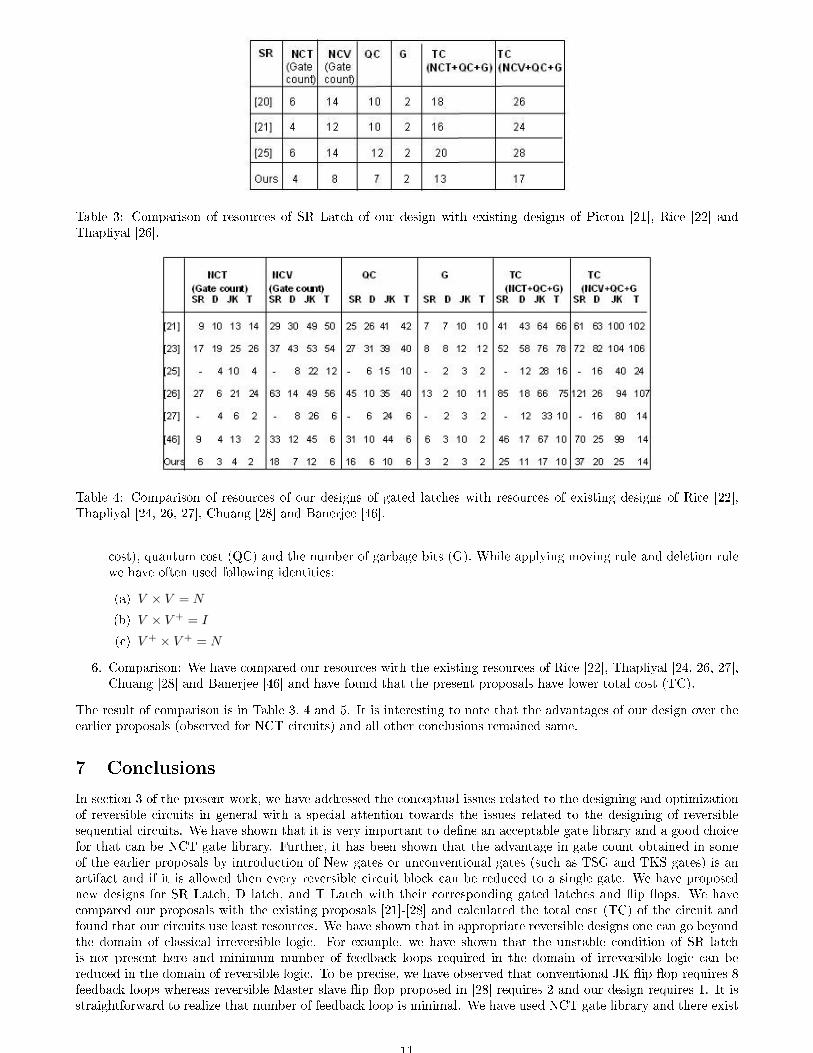
Table 3: Comparison of resources of SR Latch of our design with existing designs of Picton [21], Rice [22] andThapliyal [26].
Table 4: Comparison of resources of our designs of gated latches with resources of existing designs of Rice [22],Thapliyal [24, 26, 27], Chuang [28] and Banerjee [46].
cost), quantum cost (QC) and the number of garbage bits (G). While applying moving rule and deletion rulewe have often used following identities:
(a) V × V = N
(b) V × V + = I
(c) V + × V + = N
6. Comparison: We have compared our resources with the existing resources of Rice [22], Thapliyal [24, 26, 27],Chuang [28] and Banerjee [46] and have found that the present proposals have lower total cost (TC).
The result of comparison is in Table 3, 4 and 5. It is interesting to note that the advantages of our design over theearlier proposals (observed for NCT circuits) and all other conclusions remained same.
7 Conclusions
In section 3 of the present work, we have addressed the conceptual issues related to the designing and optimizationof reversible circuits in general with a special attention towards the issues related to the designing of reversiblesequential circuits. We have shown that it is very important to de�ne an acceptable gate library and a good choicefor that can be NCT gate library. Further, it has been shown that the advantage in gate count obtained in someof the earlier proposals by introduction of New gates or unconventional gates (such as TSG and TKS gates) is anartifact and if it is allowed then every reversible circuit block can be reduced to a single gate. We have proposednew designs for SR Latch, D latch, and T Latch with their corresponding gated latches and �ip �ops. We havecompared our proposals with the existing proposals [21]-[28] and calculated the total cost (TC) of the circuit andfound that our circuits use least resources. We have shown that in appropriate reversible designs one can go beyondthe domain of classical irreversible logic. For example, we have shown that the unstable condition of SR latchis not present here and minimum number of feedback loops required in the domain of irreversible logic can bereduced in the domain of reversible logic. To be precise, we have observed that conventional JK �ip �op requires 8feedback loops whereas reversible Master slave �ip �op proposed in [28] requires 2 and our design requires 1. It isstraightforward to realize that number of feedback loop is minimal. We have used NCT gate library and there exist
11

Table 5: Comparison of resources of our designs of �ip �ops using NCT gate library with resources of existingdesigns of Rice [22], Thapliyal [24, 26, 27] and Chuang [28].
several proposals [4, 5, 37, 38] for realization of CNOT and CCNOT gates using optical computing and CMOS basedtechnology. Thus experimentalists can easily implement our circuits. Consequently, we can easily build classicalreversible memory element. But the implementation of the present work is not limited to classical domain, this isbecause of the fact that we can also implement the proposed circuits in quantum domain with the help of opticalimplementation [37, 38]. If one aims to provide optimized reversible circuits for all the useful components of aclassical computer then this work along with the proposal of [4, 5, 37, 38] will help him to provide a complete designfor a classical reversible computer. Since it will be free from the problem of decoherence and scalability it seemsmore practical and easy to built than a real scalable quantum computer.
References
[1] R. Landuer, Irreversibility and heat generation in the computing process, IBM J. Res. Develop., 5 (1961) 183.
[2] C. H. Bennet, Logical reversibility of computation, IBM J. Res. Dev., 6 (1973) 525.
[3] M. Nielsen and I. Chuang, Quantum computation and quantum information, Cambridge University Press, NewDelhi (2002).
[4] A. De Vos et al, Design of reversible logic circuits by means of control gates, Integrated Circuit Design, LNCS,1918 (2000) 255.
[5] B. Desoete and A. De Vos, A reversible carry-look-ahead adder using control gates, Integration, VLSI J., 33(2002) 88.
[6] P. Kerntopf, A new heuristic algorithm for reversible logic synthesis, In Proceedings of the IEEE DesignAutomation Conference (2004) 834.
[7] A. Agarwal and N. K. Jha, Synthesis of reversible logic, Proceedings of IEEE, Design, Automation and Testin Europe Conference and Exhibition, 2 (2004) 1384.
[8] A. De Vos and Y. Van Rentergem, Reversible computing: from mathematical group theory to electronicalcircuit experiment, In Proceedings of the 2nd Conference on Computing Frontiers (2005).
[9] V. V. Shende, I. L. Markov, and S. S. Bullock, Synthesis of quantum logic circuits, IEEE Trans. Comput.-AidedDes. Integr. Circuits Syst., 25 (2006) 1000.
[10] M. Mohammadi and M. Eshghi, Heuristic methods to use dont cares in automated design of reversible andquantum logic circuits, Quantum Inform. Process. J. 7 (2008) 175.
[11] D. M. Miller, D. Maslov, G. W. Duek, A Transformation based algorithm for reversible logic synthesis, Pro-ceedings of 40th Design Automation conference (DAC'03), Anaheim, Califomia (2003) 318.
[12] D. Maslov et al., Quantum Circuit Simpli�cation and Level Compaction., quant-ph/0604001, (2008).
[13] M. Mohammadi and M. Eshghi, On �gures of merit in reversible and quantum logic designs, Quant. Infor.Pro., 8 (2009) 297.
[14] D. P. Vasudevan et al, Reversible-logic design with online testability, IEEE Trans. Instru. and Meas., 55 (2006)406.
12

[15] G. Schrom, Ultra-low-power CMOS technology. PhD thesis, Technischen Universitat Wien.(1998).
[16] R. C. Merkle, Two types of mechanical reversible logic. Nanotech, 4 (1993) 114.
[17] E. Knill, R. La�amme and G. J. Milburn, A scheme for e�cient quantum computation with linear optics.Nature, 409 (2001) 46.
[18] H. Wood and D. J. Chen, Fredkin gate circuits via recombination enzymes, Proceedings Evolutionary Compu-tation, 2004 (CEC2004).
[19] T. To�oli, Reversible computing, Tech memo MIT/LCS/TM-151, MIT Lab for Computer Science (1980).
[20] E. Fredkin and T. To�oli, Conservative logic, Int. J. Theo. Phys., 21 (1982) 219.
[21] P. Picton, Multi-valued sequential logic design using fredkin gates, MVL Journal, 1 (1996) 241.
[22] J. E. Rice, A New Look at Reversible Memory Elements. Proc. Int. Symp. Circuits and Systems (ISCAS), Kos,Greece, IEEE, Piscataway, NJ. (2006) 1243.
[23] J. E. Rice, An Introduction to reversible latches, The Computer Journal, 51 (2008) 700.
[24] H. Thapiyal and M. B. Shrinivas, A beginning in the reversible logic synthesis of sequential circuits, Proceedingsof MAPLD, 2005.
[25] H. Thapiyal and M. Zwolinski, Reversible logic to cryptographic hardware: A New Paradigm, Proceedingsof the 49th IEEE International Midwest Symposium on Circuits and Systems (MWSCAS 2006) Puerto Rico(2006).
[26] H. Thapliyal and A. P. Vinod, Design of reversible sequential elements with feasibility of transistor implemen-tation, Proceedings of the 2007 IEEE International Symposium on Circuits and Systems (ISCAS 2007), NewOrleans, USA, (2007) 625.
[27] H. Thapliyal, M.B Srinivas, An Extension to DNA Based Fredkin Gate Circuits: Design of Reversible SequentialCircuits using Fredkin Gates, arXiv cs/0603092.
[28] M. Chuang and C. Wang, ACM Journal on emerging technologies in computing systems, 3 (2008) 19.1.
[29] D. Maslov, G. W. Dueck and N. Scott, Reversible logic synthesis benchmark page,http://webhome.cs.uvic.ca/∼dmaslov/, (2009).
[30] A. Barenco et al., Elementary Gates for Quantum Computation, Physical Review A, 52 (1995) 3457.
[31] P. Gupta, A. Agarwal and N. K. Jha, An algorithm for synthsis of reversible logic circuits, Proceedings onComputer Aided Design of Integrated Circuits and Systems, 25 (2006) 2317.
[32] J. A. Smolin and D. P. DiVincenzo, Five two-bit quantum gates are su�cient to implement the quantumFredkin gate, Phys. Rev. A, 53 (1996) 2855.
[33] M. Mohammadi, K. Navi and M. Eshghi, Optimized reversible multiplier circuit, Journal of circuits, systemsand computers, 18 (2009) 1.
[34] M. S. Islam et al., Low cost quantum realization of reversible multiplier circuit, Infor Tech J., 8 (2009) 208.
[35] M. M. Mano, and C. R. Kime, Logic computer design fundamentals, Pearson Education, Delhi (2003).
[36] T. Sasao, Switching theory for logic synthesis, Kluwer Academic, (1999).
[37] J. L. O'Brien et al., Demonstration of an all-optical quantum controlled-NOT gate, Nature 426 (2003) 264.
[38] J. Fiurá ek, Linear-optics quantum To�oli and Fredkin gates, Phys. Rev. A, 73 (2006) 062313.
[39] H. M. Thapiyal and M. B. Srinivas, A New reversible TSG gate and its applications for designing e�cient addercircuit, 7th International Symposium on Representations and Methodologies of Future Computing Technologies(RM2005), Tokyo, Japan (2005)
[40] H. H. Babu and A. R. Chowdhury, Journal of Systems Architecture, Design of a compact reversible binarycoded decimal adder circuit, 52 (2006) 272.
[41] M. Haghparast and K. Navi, A new fault tolerant reversible gate for nanotechnology based systems, Am. J.Applied Sci., 5 (2008) 519.
13

[42] M. Haghparast et al., Design of a novel reversible multiplier circuit using HNG gate in Nanotechnology, WorldAppl. Sci. J., 3 (2008) 974.
[43] M. Haghparast and K. Navi, A novel reversible full adder circuit for nanotechnology based systems, J. AppliedSci., 7 (2007) 3995.
[44] D. Aharonov, A simple proof that to�oli and hadamard are quantum universal, quant-ph/0301040v1 (2003).
[45] A. Yu. Kitaev, Quantum computations:Algorithms and error correction, Russian math, 6 (1997) 1191.
[46] A. Banerjee and A. Pathak, On the synthesis of sequential rcircuits, quant-ph, 0707.4233v1.
[47] D. Maslov and G. W. Duek, Garbage in reversible design of multiple output functions, Proc. of 6th InternationalSymposium on Representations and Methodology of Future Computing Technologies, (2003) 162.
14