
Real-time GNSS spoofing detection in maritime code receivers
Upload
khangminh22Category
view
1download
0
New Concepts in Front End Design for Receivers withLarge, Multiband Tuning Ranges
S. M. Shajedul Hasan
Dissertation submitted to the Faculty of theVirginia Polytechnic Institute and State University
in partial fulfillment of the requirements for the degree of
Doctor of Philosophyin
Electrical Engineering
Committee Members:
Dr. Steven W. Ellingson, ChairDr. R. Michael Buehrer
Dr. Jeffrey H. ReedDr. William A. DavisDr. John H. Simonetti
April 3, 2009Blacksburg, Virginia
Keywords: RF Multiplexer, Multiband Multimode Radio, Public Safety Radio, WidebandReceiver
Copyright 2009, S. M. Shajedul Hasan

New Concepts in Front End Design for Receivers with Large,
Multiband Tuning Ranges
S. M. Shajedul Hasan
Abstract
This dissertation presents new concepts in front end design for receivers with large, multiband
tuning ranges. Such receivers are required to support large bandwidths (up to 10’s of MHz) over
very large tuning ranges (30:1 and beyond) with antennas that are usually narrowband, or which
at best support multiple narrow bandwidths. Traditional techniques to integrate a single antenna
with such receivers are limited in their ability to handle simultaneous channels distributed over very
large tuning ranges, which is important for frequency-agile cognitive radio, surveillance, and other
applications requiring wideband or multiband monitoring. Direct conversion architecture is gaining
popularity due to the recent advancements in CMOS–based RFIC technology. The possibility of
multiple parallel transceivers in RF CMOS suggests an approach to antenna–receiver integration
using multiplexers. This dissertation describes an improved use of multiplexers to integrate anten-
nas to receivers. First, the notion of sensitivity–constrained design is considered. In this approach,
the goal is first to achieve sensitivity which is nominally dominated by external (environmental)
noise, and then secondly to improve bandwidth to the maximum possible consistent with this goal.
Next, a procedure is developed for designing antenna-multiplexer-preamplifier assemblies using this
philosophy. It is shown that the approach can significantly increase the usable bandwidth and num-
ber of bands that can be supported by a single, traditional antenna. This performance is verified
through field experiments. A prototype multiband multimode radio for public safety applications
using these concepts is designed and demonstrated.

This dissertation is dedicated to
my mother Hasina Sardar, my wife Rimi Ferdous,
and my advisors:
Dr. S. W. Ellingson, Dr. M. K. Howlader, Dr. Y. W. Kang, & Dr. S. M. L. Kabir
iii

Acknowledgments
I am very grateful to God who helped and guided me throughout my life and made it possible. I
could never have reached to this point without Him.
My advisor, Dr. Steven Ellingson, has a tremendous contribution in achievement of this important
milestone in my life. I am really grateful to him for his continuous guidance and patience help
throughout my student life at Virginia Tech. His depth of technical knowledge and engineering
skills really helped me to advance my research. This dissertation will not be in this shape without
his constructive comments and editing. I am feeling lucky to be a student of him.
I am also thankful to my committee members Dr. Jeffrey H. Reed, Dr. R. Michael Buehrer, Dr.
William A. Davis, and Dr. John H. Simonetti for their valuable time and feedback. Special thanks
to Dr. Reed, whose “Software Radio” class helped me to understand many fundamental topics
related to SDR area. I would also like to give my thanks to Dr. Davis for his guidance when I was
a teaching assistant in his “Radio Engineering” course. My thanks also goes to Dr. Buehrer for
participating in my qualifying exam.
I am also thankful to the people of Motorola who provides us an RFIC chip which is used in this
dissertation. I am really grateful to Mr. Gio Cafaro, Mr. Bob Stengel, and Dr. Neiyer Correal for
their patience help and guidance.
My thanks go to my colleague Ms. Kshitija Deshpande for allowing me to use her antenna temper-
ature calculation code discussed in Section 4.4.4 in this dissertation. I also would like to give my
thanks to Mr. Mahmud Harun for his help in some of my measurements. My heartiest thanks go
to Mr. Rithirong Thandee, Mr. Philip Balister, and Ms. Qian Liu for their contribution to design
iv

the user interface of the multiband radio described in this document.
I would like to convey my special thanks to my colleague Dr. Kyehun Lee for his help to make
me understand many fundamental topics in my research area. Also many thanks to Mr. Taeyoung
Yang of Virginia Tech Antenna Group (VTAG) for his generous help in some of my antenna
measurement. I am also grateful to the people of VTAG for allowing me to use their facility for
some of my measurements. I also would like to mention one of my former colleague Dr. Christopher
Anderson for his help to make me learn the layout software Mentor Graphics. My special thanks
to Dr. Siddik Yarman from Istanbul University for his help to make me understand the concept of
RFT matching.
Many thanks to the people of MPRG lab who helped me during my studies and research at Virginia
Tech, such as Ms. Hilda Reynolds, Ms. Nancy Goad, Ms. Jenny Frank, and Mr. James Dunson.
This work was funded in part by the National Institute of Justice of the U.S. Department of Justice
under grant number 2005–IJ–CX–K018 and in part by the Office of Naval Research via contract
number N00014-07-C-0147.
v

Contents
1 Introduction 1
1.1 Multiband Multimode Radio (MMR) . . . . . . . . . . . . . . . . . . . . . . . . . . . 2
1.2 Application Example: Public Safety . . . . . . . . . . . . . . . . . . . . . . . . . . . 3
1.3 Traditional Front End Design . . . . . . . . . . . . . . . . . . . . . . . . . . . . . . . 7
1.4 Current Trends in Front End Design . . . . . . . . . . . . . . . . . . . . . . . . . . . 9
1.5 Problem Statement . . . . . . . . . . . . . . . . . . . . . . . . . . . . . . . . . . . . . 10
1.6 Contributions . . . . . . . . . . . . . . . . . . . . . . . . . . . . . . . . . . . . . . . . 11
1.7 Organization of this Dissertation . . . . . . . . . . . . . . . . . . . . . . . . . . . . . 12
2 Receiver Design Fundamentals & Trends 14
2.1 Anatomy of a Radio . . . . . . . . . . . . . . . . . . . . . . . . . . . . . . . . . . . . 14
2.2 Antennas . . . . . . . . . . . . . . . . . . . . . . . . . . . . . . . . . . . . . . . . . . 16
2.3 Receiver System Design Parameters . . . . . . . . . . . . . . . . . . . . . . . . . . . 20
2.3.1 Digitization . . . . . . . . . . . . . . . . . . . . . . . . . . . . . . . . . . . . . 20
2.3.2 Sensitivity and Gain . . . . . . . . . . . . . . . . . . . . . . . . . . . . . . . . 22
2.3.3 Linearity . . . . . . . . . . . . . . . . . . . . . . . . . . . . . . . . . . . . . . 23
2.3.4 Selectivity . . . . . . . . . . . . . . . . . . . . . . . . . . . . . . . . . . . . . . 26
2.4 Receiver Architectures . . . . . . . . . . . . . . . . . . . . . . . . . . . . . . . . . . . 28
2.4.1 Superheterodyne Architecture . . . . . . . . . . . . . . . . . . . . . . . . . . . 29
2.4.2 Direct Sampling Architecture . . . . . . . . . . . . . . . . . . . . . . . . . . . 30
2.4.3 Direct Conversion Architecture . . . . . . . . . . . . . . . . . . . . . . . . . . 31
2.4.4 Modern Techniques to Overcome Direct Conversion Limitations . . . . . . . . 33
vi

2.5 New Possibilities for MMR with RFICs . . . . . . . . . . . . . . . . . . . . . . . . . 36
2.6 Summary . . . . . . . . . . . . . . . . . . . . . . . . . . . . . . . . . . . . . . . . . . 38
3 Antenna–Receiver Interfacing 41
3.1 Antenna Matching & Parameters . . . . . . . . . . . . . . . . . . . . . . . . . . . . . 41
3.2 Fundamental Limitations . . . . . . . . . . . . . . . . . . . . . . . . . . . . . . . . . 45
3.2.1 Bode–Fano Limit . . . . . . . . . . . . . . . . . . . . . . . . . . . . . . . . . . 45
3.2.2 Foster’s Reactance Theorem . . . . . . . . . . . . . . . . . . . . . . . . . . . . 48
3.3 Wideband Matching using Passive Components . . . . . . . . . . . . . . . . . . . . . 48
3.3.1 Analytical Techniques . . . . . . . . . . . . . . . . . . . . . . . . . . . . . . . 50
3.3.2 Real Frequency Technique . . . . . . . . . . . . . . . . . . . . . . . . . . . . . 54
3.4 Antenna Tuning using Variable Reactors . . . . . . . . . . . . . . . . . . . . . . . . . 55
3.5 Non-Foster Impedance Matching . . . . . . . . . . . . . . . . . . . . . . . . . . . . . 58
3.6 Summary . . . . . . . . . . . . . . . . . . . . . . . . . . . . . . . . . . . . . . . . . . 60
4 Sensitivity-Constrained Front-End Design 61
4.1 Noise Characterization . . . . . . . . . . . . . . . . . . . . . . . . . . . . . . . . . . . 62
4.1.1 Sources of Noise . . . . . . . . . . . . . . . . . . . . . . . . . . . . . . . . . . 62
4.1.2 Noise Modeling . . . . . . . . . . . . . . . . . . . . . . . . . . . . . . . . . . . 63
4.1.3 Characterization of Environmental Noise . . . . . . . . . . . . . . . . . . . . 64
4.2 Optimum Noise Figure Specification . . . . . . . . . . . . . . . . . . . . . . . . . . . 69
4.3 Implications for Design of Antenna Matching . . . . . . . . . . . . . . . . . . . . . . 72
4.4 Experimental Verification . . . . . . . . . . . . . . . . . . . . . . . . . . . . . . . . . 74
4.4.1 Experiment Design . . . . . . . . . . . . . . . . . . . . . . . . . . . . . . . . . 76
4.4.2 Antenna Design . . . . . . . . . . . . . . . . . . . . . . . . . . . . . . . . . . . 79
4.4.3 Data Collection . . . . . . . . . . . . . . . . . . . . . . . . . . . . . . . . . . . 84
4.4.4 Results . . . . . . . . . . . . . . . . . . . . . . . . . . . . . . . . . . . . . . . 89
4.5 Summary . . . . . . . . . . . . . . . . . . . . . . . . . . . . . . . . . . . . . . . . . . 94
5 Multiplexer Design 95
5.1 Classical Multiplexer Design Theory . . . . . . . . . . . . . . . . . . . . . . . . . . . 96
vii

5.2 Research Trends in Multiplexer Design . . . . . . . . . . . . . . . . . . . . . . . . . . 103
5.3 Sensitivity-Constrained Multiplexer Design . . . . . . . . . . . . . . . . . . . . . . . 104
5.4 VHF Monopole Multiplexer Design Example . . . . . . . . . . . . . . . . . . . . . . 106
5.4.1 Problem Statement . . . . . . . . . . . . . . . . . . . . . . . . . . . . . . . . . 106
5.4.2 Multiplexer Design . . . . . . . . . . . . . . . . . . . . . . . . . . . . . . . . . 107
5.4.3 Experiment Design . . . . . . . . . . . . . . . . . . . . . . . . . . . . . . . . . 120
5.4.4 Data Collection . . . . . . . . . . . . . . . . . . . . . . . . . . . . . . . . . . . 123
5.4.5 Results . . . . . . . . . . . . . . . . . . . . . . . . . . . . . . . . . . . . . . . 123
5.5 Summary . . . . . . . . . . . . . . . . . . . . . . . . . . . . . . . . . . . . . . . . . . 128
6 Multiplexer Application to a Multiband Multimode Radio 129
6.1 Multiplexer Design for a Generic Monopole Antenna . . . . . . . . . . . . . . . . . . 129
6.1.1 Optimization . . . . . . . . . . . . . . . . . . . . . . . . . . . . . . . . . . . . 130
6.1.2 Results . . . . . . . . . . . . . . . . . . . . . . . . . . . . . . . . . . . . . . . 137
6.2 Multiplexer Design for a Real Antenna . . . . . . . . . . . . . . . . . . . . . . . . . . 138
6.2.1 Optimization . . . . . . . . . . . . . . . . . . . . . . . . . . . . . . . . . . . . 142
6.2.2 Results . . . . . . . . . . . . . . . . . . . . . . . . . . . . . . . . . . . . . . . 142
6.2.3 Implementation and Lab Results . . . . . . . . . . . . . . . . . . . . . . . . . 147
6.3 Summary . . . . . . . . . . . . . . . . . . . . . . . . . . . . . . . . . . . . . . . . . . 148
7 Design & Development of a Multiband Multimode Radio 154
7.1 Overview of the Project . . . . . . . . . . . . . . . . . . . . . . . . . . . . . . . . . . 156
7.2 Original Superhet Architecture . . . . . . . . . . . . . . . . . . . . . . . . . . . . . . 156
7.2.1 RF Downconverter (RFDC) . . . . . . . . . . . . . . . . . . . . . . . . . . . . 158
7.2.2 RF Upconverter (RFUC) . . . . . . . . . . . . . . . . . . . . . . . . . . . . . 160
7.3 Motorola RFIC: Description & Performance Analysis . . . . . . . . . . . . . . . . . . 162
7.3.1 Overview of the Motorola RFIC . . . . . . . . . . . . . . . . . . . . . . . . . 162
7.3.2 RFIC Evaluation Board . . . . . . . . . . . . . . . . . . . . . . . . . . . . . . 163
7.3.3 Receiver Measurement Results . . . . . . . . . . . . . . . . . . . . . . . . . . 167
7.4 Direct Conversion Architecture . . . . . . . . . . . . . . . . . . . . . . . . . . . . . . 170
viii

7.5 Prototype Design . . . . . . . . . . . . . . . . . . . . . . . . . . . . . . . . . . . . . . 172
7.5.1 RFFE Board . . . . . . . . . . . . . . . . . . . . . . . . . . . . . . . . . . . . 172
7.5.2 RFIC Board . . . . . . . . . . . . . . . . . . . . . . . . . . . . . . . . . . . . 172
7.5.3 ADC/DAC Board . . . . . . . . . . . . . . . . . . . . . . . . . . . . . . . . . 175
7.5.4 FPGA Board . . . . . . . . . . . . . . . . . . . . . . . . . . . . . . . . . . . . 176
7.5.5 GNI Analysis . . . . . . . . . . . . . . . . . . . . . . . . . . . . . . . . . . . . 177
7.5.6 Current Status . . . . . . . . . . . . . . . . . . . . . . . . . . . . . . . . . . . 178
7.6 Summary . . . . . . . . . . . . . . . . . . . . . . . . . . . . . . . . . . . . . . . . . . 180
8 Conclusions 182
8.1 Findings . . . . . . . . . . . . . . . . . . . . . . . . . . . . . . . . . . . . . . . . . . . 182
8.2 Future Work . . . . . . . . . . . . . . . . . . . . . . . . . . . . . . . . . . . . . . . . 184
A Relationship Between Predetection SNR and SINAD 186
B GNI Analysis 189
C VHF Multiplexer Board 191
D Superheterodyne Downconverter 196
E RF Front End Board 202
E.1 Board Overview . . . . . . . . . . . . . . . . . . . . . . . . . . . . . . . . . . . . . . . 202
E.2 Layout, and Bill of Materials . . . . . . . . . . . . . . . . . . . . . . . . . . . . . . . 207
F RFIC Board 216
F.1 Board Overview . . . . . . . . . . . . . . . . . . . . . . . . . . . . . . . . . . . . . . . 216
F.2 Schematic, Layout, and Bill of Materials . . . . . . . . . . . . . . . . . . . . . . . . . 219
G ADC/DAC Board 232
G.1 Board Overview . . . . . . . . . . . . . . . . . . . . . . . . . . . . . . . . . . . . . . . 232
G.2 Layout, and Bill of Materials . . . . . . . . . . . . . . . . . . . . . . . . . . . . . . . 239
H Audio Board & User Interface 247
ix

I Copyright Permissions 256
Bibliography 257
x

List of Figures
1.1 Illustration of multiband multimode radio using (a) different chipsets for variousbands/modes, (b) one single chipset for all bands/modes. Adopted from an illus-tration by Bitwave Semiconductor (www.bitwave.com) (used with permission, seeAppendix I). . . . . . . . . . . . . . . . . . . . . . . . . . . . . . . . . . . . . . . . . 4
1.2 Interoperability between two disparate radio networks. (a) Two groups, using in-compatible bands/modes. (b) Network-based interoperability. (c) Introducing a newuncoordinated user. (d) User-based interoperability. . . . . . . . . . . . . . . . . . . 6
1.3 Receiver section of VX-7R multiband radio [13]. . . . . . . . . . . . . . . . . . . . . 8
1.4 Antenna impedance of VX-7R multiband radio (measured by the author with theassistance of Virgina Tech Antenna Group). . . . . . . . . . . . . . . . . . . . . . . . 8
1.5 Calculated IME (loss due to reflection at the antenna–receiver interface) betweenthe VX-7R antenna and a preamplifier with input impedance 50Ω. . . . . . . . . . . 9
2.1 Block diagram of a typical radio. . . . . . . . . . . . . . . . . . . . . . . . . . . . . . 15
2.2 Circuit model for antenna during transmission of signals. . . . . . . . . . . . . . . . 17
2.3 Circuit model for antenna during reception of signals. . . . . . . . . . . . . . . . . . 19
2.4 TTG circuit model for ZA for a dipole antenna. . . . . . . . . . . . . . . . . . . . . . 20
2.5 Graphical explanation of P1, IIP2, and IIP3. . . . . . . . . . . . . . . . . . . . . . . 25
2.6 Intermodulation products. . . . . . . . . . . . . . . . . . . . . . . . . . . . . . . . . . 26
2.7 Simple receive system for linearity–sensitivity trade-off analysis. . . . . . . . . . . . . 27
2.8 Sensitivity (MDS) and IIP3 versus attenuator setting for the simple receiver modelshown in Figure 2.7 . . . . . . . . . . . . . . . . . . . . . . . . . . . . . . . . . . . . . 27
2.9 N -channel multiplexer using bandpass filters. . . . . . . . . . . . . . . . . . . . . . . 28
2.10 A single–conversion superheterodyne receiver architecture. . . . . . . . . . . . . . . . 30
2.11 Block diagram of a direct sampling receiver. . . . . . . . . . . . . . . . . . . . . . . . 31
2.12 Block diagram of a direct conversion receiver. . . . . . . . . . . . . . . . . . . . . . . 33
xi

2.13 LO leakage and interface leakage in a direct conversion receiver (shown for one base-band section only). . . . . . . . . . . . . . . . . . . . . . . . . . . . . . . . . . . . . . 34
2.14 Illustration of chopper stabilization technique. . . . . . . . . . . . . . . . . . . . . . . 35
2.15 RF block with a differential input and output. . . . . . . . . . . . . . . . . . . . . . . 36
2.16 Illustration of differential implementation of the chopper stabilization technique. . . 37
2.17 Functional block diagram of the Motorola RFIC version 4 (used with permission, seeAppendix I). . . . . . . . . . . . . . . . . . . . . . . . . . . . . . . . . . . . . . . . . 39
2.18 Possible architectures to design a MMR using multiplexer and RFICs. . . . . . . . . 40
3.1 General configuration for antenna matching. . . . . . . . . . . . . . . . . . . . . . . . 42
3.2 Block diagram to calculate transducer power gain. . . . . . . . . . . . . . . . . . . . 44
3.3 Illustration of the Bode-Fano limit. . . . . . . . . . . . . . . . . . . . . . . . . . . . . 47
3.4 Matching bandwidth for various VSWR estimated using an approximate form of theBode–Fano bound for a monopole antenna 20 cm long with 5 mm radius. . . . . . . 49
3.5 Configuration to demonstrate the matching techniques. . . . . . . . . . . . . . . . . 50
3.6 Four element matching network using method in [47]. . . . . . . . . . . . . . . . . . 52
3.7 Performance (TPG) of the four element matching network. . . . . . . . . . . . . . . 52
3.8 Matching circuit calculated using RFT method. . . . . . . . . . . . . . . . . . . . . . 56
3.9 Performance (TPG) of the matching circuit calculated using RFT method. Compareto Figure 3.7. . . . . . . . . . . . . . . . . . . . . . . . . . . . . . . . . . . . . . . . . 57
3.10 Antenna tuning using variable reactors. . . . . . . . . . . . . . . . . . . . . . . . . . 57
3.11 Matching a capacitive reactance (such as that of an electrically small monopole)using (a) traditional matching, (b) non-Foster matching (adapted from [66]). . . . . 59
3.12 Basic NIC circuit using op-amp. . . . . . . . . . . . . . . . . . . . . . . . . . . . . . 59
4.1 PSD of various noise environments calculated using the data provided in [73]. . . . . 63
4.2 Modeling external noise of an antenna immersed in external noise temperature TA. . 64
4.3 Median noise figures for various external noise sources using the model provided in [73]. 66
4.4 Median noise figures for various external noise sources using the model presented inTable 4.2. . . . . . . . . . . . . . . . . . . . . . . . . . . . . . . . . . . . . . . . . . . 68
xii

4.5 Example of the optimum noise figure specification. Lines with markers show themaximum noise figure for which the sensitivity of a receiver is limited by the noisegenerated by its own front end (by a factor of 10 over external noise) in 95% of loca-tions that can be classified as the indicated type. The irreducible mean contributionfrom the combination of Galactic background noise and the CMB is also shown. . . 71
4.6 Contributions to the PSD at the preamplifier output for a lossless antenna (η = 1)by Galactic noise. In this plot, preamplifier gain and noise figure are chosen to beGp = +22 dB and F = 3.0 dB, respectively. . . . . . . . . . . . . . . . . . . . . . . . 73
4.7 Same as Figure 4.6, but now assuming “Residential” noise. . . . . . . . . . . . . . . 75
4.8 Block diagram of the field experiment setup. . . . . . . . . . . . . . . . . . . . . . . . 77
4.9 Image of the components used in the receiver (the part which is close to antenna)during the field experiment. . . . . . . . . . . . . . . . . . . . . . . . . . . . . . . . . 78
4.10 The components used in the receiver (the part which is close to data acquisition) ofthe field experiment. . . . . . . . . . . . . . . . . . . . . . . . . . . . . . . . . . . . . 78
4.11 Transfer function of the receiver used in the field experiment. . . . . . . . . . . . . . 80
4.12 The dimensions of the monopole antenna used in the field experiment. . . . . . . . . 82
4.13 The dimensions of the ground screen used in the field measurement as well as in thesimulation. . . . . . . . . . . . . . . . . . . . . . . . . . . . . . . . . . . . . . . . . . 83
4.14 Antenna construction details. . . . . . . . . . . . . . . . . . . . . . . . . . . . . . . . 84
4.15 Simulated and measured impedance of the VHF monopole antenna. . . . . . . . . . 85
4.16 Calculated IME between the VHF monopole antenna and a preamplifier with Zp =50Ω using both the simulated and measured antenna impedance. . . . . . . . . . . . 86
4.17 Antenna and ground screen setup during the field experiment. . . . . . . . . . . . . . 87
4.18 Measured integrated PSD at the input of spectrum analyzer. Integrated over 500ms with 1 kHz spectral resolution. . . . . . . . . . . . . . . . . . . . . . . . . . . . . 88
4.19 PSD referenced to the antenna terminals. . . . . . . . . . . . . . . . . . . . . . . . . 91
4.20 Antenna efficiency (η) assuming realistic ground with the ground screen shown inFigure 4.13 on it. . . . . . . . . . . . . . . . . . . . . . . . . . . . . . . . . . . . . . . 92
4.21 Ratio of the predicted to the measured PSD. . . . . . . . . . . . . . . . . . . . . . . 93
5.1 Circuit diagram of a diplexer. Each of the channels are designed for 50Ω terminationimpedance. . . . . . . . . . . . . . . . . . . . . . . . . . . . . . . . . . . . . . . . . . 97
xiii

5.2 Performance (TPG) of the diplexer in Figure 5.1, assuming 50Ω source impedance.Each channels are designed for 50Ω termination impedance. Solid lines representthe results when the input ports of the diplexer channels are connected together anddotted lines represent the results when each of the channels are connected with thesource separately. . . . . . . . . . . . . . . . . . . . . . . . . . . . . . . . . . . . . . . 98
5.3 A parallel–connected multiplexer. . . . . . . . . . . . . . . . . . . . . . . . . . . . . . 99
5.4 A series–connected multiplexer. . . . . . . . . . . . . . . . . . . . . . . . . . . . . . . 100
5.5 Multiplexer with parallel connected channels, input of which is connected with amatching circuit and an antenna. . . . . . . . . . . . . . . . . . . . . . . . . . . . . . 102
5.6 Multiplexer interfacing concept. . . . . . . . . . . . . . . . . . . . . . . . . . . . . . . 107
5.7 Circuit topology of each multiplexer channel. The inputs of the three channels areconnected in parallel. . . . . . . . . . . . . . . . . . . . . . . . . . . . . . . . . . . . . 108
5.8 Performance (TPG) of the initial (50Ω–in, 50Ω–out) multiplexer, assuming constant50Ω source impedance. Solid lines represent the results when input port of all mul-tiplexer channels are connected together and dotted lines represent the results wheneach of the channels are connected with the source separately. . . . . . . . . . . . . . 109
5.9 Performance (TPG) of initial (50Ω–in, 50Ω–out) multiplexer, assuming the simulatedimpedance of the VHF monopole. Solid lines represent the results when input portsof all multiplexer channels are connected together and dotted lines represent theresults when each of the channels are connected with the source separately. . . . . . 110
5.10 Antenna impedance calculated from center frequency series RC or series RL approx-imation (as appropriate) of the VHF monopole antenna. Solid lines represents theapproximation and dotted lines represent the original value. . . . . . . . . . . . . . . 112
5.11 Performance (TPG) of optimized multiplexer, assuming simulated impedance ofVHF monopole. Solid lines represent the results after optimization and dotted linesrepresent the results before optimization. . . . . . . . . . . . . . . . . . . . . . . . . 114
5.12 Performance (TPG) comparison of optimized multiplexer for original and standardcomponent values. Solid lines represent the performance using standard componentvalues and dotted lines represent the performance using original values. . . . . . . . 115
5.13 Performance (γ) of optimized multiplexer (using standard component values) for 2,3, and 4 dB preamplifier noise figures, assuming simulated impedance of the VHFmonopole antenna and Celestial noise. . . . . . . . . . . . . . . . . . . . . . . . . . . 116
5.14 Performance (γ) of optimized multiplexer (using standard component values) for 2,3, and 4 dB preamplifier noise figures, assuming simulated impedance of the VHFmonopole antenna and “Residential” noise. . . . . . . . . . . . . . . . . . . . . . . . 117
xiv

5.15 Lab measurement of the optimized (standard component values given in Table 5.3)multiplexer assuming 50Ω source and load impedances. Solid lines represent themeasurement results and dashed lines are the results from simulation. (Note thatthis result is not representative of actual performance, since the source impedance is50Ω as opposed to ZA). Three channels are measured separately and shown on thesame plot. . . . . . . . . . . . . . . . . . . . . . . . . . . . . . . . . . . . . . . . . . . 119
5.16 Predicted TPG of the optimized multiplexer assuming the simulated antenna impedanceas source, and using the S21 measurements described in the text. Solid lines repre-sent the resulting TPG and dashed lines represent the same result using S21 fromthe simulation. . . . . . . . . . . . . . . . . . . . . . . . . . . . . . . . . . . . . . . . 120
5.17 Performance (γ) of optimized implemented multiplexer (using standard components)for 2, 3, and 4 dB preamplifier noise figures, assuming simulated impedance of theVHF monopole antenna and Celestial noise as external noise environment, based onthe S21 measurements described in the text. . . . . . . . . . . . . . . . . . . . . . . . 121
5.18 Analysis of the experiment used to determine multiplexer channel TPG. . . . . . . . 122
5.19 The multiplexer in the process of field testing. . . . . . . . . . . . . . . . . . . . . . . 124
5.20 Measured integrated PSD for each multiplexer channel, and also without the multi-plexer. Integrated over 500 ms with 1 kHz spectral resolution. . . . . . . . . . . . . . 125
5.21 Performance (TPG) of the multiplexer as built with standard component values.Solid lines represent the measured TPG from the field experiment and dotted linesrepresent the predicted TPG based on the S21 measurements shown in Figure 5.16. 126
5.22 Ratio of the predicted to the measured TPG. . . . . . . . . . . . . . . . . . . . . . . 127
6.1 Interfacing concept of the multiplexer designed for the VT MMR. . . . . . . . . . . . 131
6.2 Circuit topology of each multiplexer channel in the VT MMR. The inputs of the fourchannels are connected in parallel. . . . . . . . . . . . . . . . . . . . . . . . . . . . . 131
6.3 Performance (TPG) of initial (50Ω–in, 50Ω–out) multiplexer designed for the VTMMR, assuming constant 50Ω antenna impedance. . . . . . . . . . . . . . . . . . . . 132
6.4 Circuit model used to calculate the impedance of generic rod antenna using the TTGmodel. . . . . . . . . . . . . . . . . . . . . . . . . . . . . . . . . . . . . . . . . . . . . 133
6.5 Impedance of the generic rod antenna. Solid lines represent the result using TTGmodel and dotted lines represent the result using the method of moments. . . . . . . 134
6.6 Calculated IME between the antenna and a preamplifier with Zp = 50Ω. The solidline represents the result using the generic rod antenna (TTG circuit model) andthe dotted lines represents the result using antenna impedance simulated from themethod of moments. . . . . . . . . . . . . . . . . . . . . . . . . . . . . . . . . . . . . 135
xv

6.7 Antenna impedance calculated from series RC or series RL approximation of the rodantenna. Solid lines represent the series RC or RL approximation and the dottedlines represent the actual values. . . . . . . . . . . . . . . . . . . . . . . . . . . . . . 136
6.8 Performance (TPG) of the optimized multiplexer designed for the generic rod an-tenna. Solid lines represent the results after optimization and dotted lines representthe results before optimization. . . . . . . . . . . . . . . . . . . . . . . . . . . . . . . 138
6.9 Performance (γ) of optimized multiplexer for the generic rod antenna, assumingCelestial noise environment. . . . . . . . . . . . . . . . . . . . . . . . . . . . . . . . . 139
6.10 Performance (γ) of the optimized multiplexer for the generic rod antenna, assuming“Residential” noise environment. . . . . . . . . . . . . . . . . . . . . . . . . . . . . . 140
6.11 Noise PSD at the output of the preamplifier referenced to antenna terminals (rodantenna). Assuming “Residential” noise as external noise source and a preamplifierwith 2 dB noise figure. . . . . . . . . . . . . . . . . . . . . . . . . . . . . . . . . . . . 141
6.12 The exact dimensions of antenna, Model ANT-418-CW-QW from Antenna Factor,Inc. [89] (used with permission, see Appendix I). Units in parentheses are in mm. . . 143
6.13 Measured impedance of antenna, Model ANT-418-CW-QW from Antenna Factor, Inc.144
6.14 Calculated IME between the antenna, Model ANT-418-CW-QW from Antenna Fac-tor, Inc., and a preamplifier with Zp = 50Ω using the measured antenna impedance. 145
6.15 Antenna impedance calculated from series RC or series RL approximation of theANT-418-CW-QW. Solid lines represent the approximation and dotted lines repre-sent the actual values. . . . . . . . . . . . . . . . . . . . . . . . . . . . . . . . . . . . 146
6.16 Performance (TPG) of the optimized multiplexer (using standard component values)designed for the ANT-418-CW-QW. Solid lines represent the results after optimiza-tion and dotted lines represent the results before optimization. . . . . . . . . . . . . 149
6.17 Performance (γ) of optimized multiplexer (using standard component values) for theANT-418-CW-QW, assuming Celestial noise environment only. . . . . . . . . . . . . 150
6.18 Performance (γ) of optimized multiplexer (using standard component values) for theANT-418-CW-QW, assuming “Residential” noise environment. . . . . . . . . . . . . 151
6.19 Noise PSD at the output of the preamplifier referenced to antenna ANT-418-CW-QW terminals assuming “Residential” noise environment and a preamplifier with 2dB noise figure. Using standard component values in the multiplexer. . . . . . . . . 152
6.20 Lab measurement of the optimized (using standard component values given in Ta-ble 6.5) multiplexer designed for the ANT-418-CW-QW, using instead 50Ω sourceand load impedances. Solid lines represent the measurement results and dashed linesare the results from simulation. (Note that this result is not representative of actualperformance, since the source impedance is 50Ω as opposed to ZA). . . . . . . . . . . 153
7.1 VT MMR prototype. . . . . . . . . . . . . . . . . . . . . . . . . . . . . . . . . . . . . 155
xvi

7.2 Original strawman design for the VT MMR using superhet architecture. . . . . . . . 159
7.3 Block diagram of the superhet–based RF downconverter designed for the VT MMR. 160
7.4 RFDC developed for the original (superhet–based) VT MMR. . . . . . . . . . . . . . 161
7.5 RFUC developed for the superhet–based VT MMR. . . . . . . . . . . . . . . . . . . 161
7.6 VT evaluation board for Motorola RFIC version 4. The IC itself is the square chipin the center of the board. . . . . . . . . . . . . . . . . . . . . . . . . . . . . . . . . . 164
7.7 Snapshot of the LabView program used to configure the RFIC through an SPI link. 165
7.8 Gain measured in the first receiver port of the RFIC. . . . . . . . . . . . . . . . . . . 168
7.9 Input 1 dB compression point measured in the first receiver port of the RFIC. . . . . 169
7.10 Image rejection measured in the first receiver port of the RFIC. . . . . . . . . . . . . 169
7.11 System diagram of the final VT MMR prototype (using the Motorola RFIC). . . . . 171
7.12 RFFE board for the VT MMR (top view); ground screen side. . . . . . . . . . . . . 173
7.13 RFFE board for the VT MMR (bottom view); component side. . . . . . . . . . . . . 173
7.14 Block diagram of the RFFE board. . . . . . . . . . . . . . . . . . . . . . . . . . . . . 174
7.15 RFIC board for the VT MMR. . . . . . . . . . . . . . . . . . . . . . . . . . . . . . . 175
7.16 ADC/DAC board for the VT MMR (frequency synthesizer on reverse side). . . . . . 176
A.1 Audio SNR as a function of predetection SNR for analog FM (B = 12.5 kHz). . . . . 188
B.1 Block diagram of a general receiver chain for GNI analysis. All the component valuesare in linear units (i.e., not dB). . . . . . . . . . . . . . . . . . . . . . . . . . . . . . 189
C.1 Schematic of the multiplexer designed for the VHF monopole antenna. . . . . . . . . 192
C.2 Top layer of the multiplexer board designed for the VHF monopole antenna. . . . . . 193
D.1 Schematic of the superheterodyne RF downconverter board designed for the initialVT MMR prototype (continues in Figure D.2). . . . . . . . . . . . . . . . . . . . . . 197
D.2 Schematic of the superheterodyne RF downconverter board designed for the initialVT MMR prototype (continued from Figure D.1). . . . . . . . . . . . . . . . . . . . 198
D.3 Top layer of the superheterodyne RF downconverter board designed for the initialVT MMR prototype. . . . . . . . . . . . . . . . . . . . . . . . . . . . . . . . . . . . . 199
E.1 Summary of input/output ports of the RFFE board. . . . . . . . . . . . . . . . . . . 203
E.2 Schematic of the multiplexer and switch section of the RFFE board. . . . . . . . . . 204
xvii

E.3 Schematic of the amplifier section of the RFFE board. . . . . . . . . . . . . . . . . . 205
E.4 Schematic of the attenuator section of the RFFE board. . . . . . . . . . . . . . . . . 206
E.5 Frequency responses of the 5th order Chebyshev filters implemented in the RFFEboard. . . . . . . . . . . . . . . . . . . . . . . . . . . . . . . . . . . . . . . . . . . . . 208
E.6 Schematic of the power supply section of the RFFE board. . . . . . . . . . . . . . . 209
E.7 Top layer (also ground plane for antenna) of the RFFE board. . . . . . . . . . . . . 210
E.8 Bottom layer (component side) of the RFFE board. . . . . . . . . . . . . . . . . . . 211
F.1 Summary of input/output ports of the RFIC board. . . . . . . . . . . . . . . . . . . 217
F.2 Schematic of the RFIC section of the RFIC board. . . . . . . . . . . . . . . . . . . . 220
F.3 Schematic of the baseband section of the RFIC board. . . . . . . . . . . . . . . . . . 221
F.4 Schematic of the receiver section of the RFIC board. . . . . . . . . . . . . . . . . . . 222
F.5 Schematic of the transmitter section of the RFIC board. . . . . . . . . . . . . . . . . 223
F.6 Schematic of the power supply section of the RFIC board. . . . . . . . . . . . . . . . 224
F.7 Schematic of the SPI section of the RFIC board. . . . . . . . . . . . . . . . . . . . . 225
F.8 Top layer of the RFIC board. . . . . . . . . . . . . . . . . . . . . . . . . . . . . . . . 226
F.9 Bottom layer of the RFIC board. . . . . . . . . . . . . . . . . . . . . . . . . . . . . . 227
F.10 Power layer of the RFIC board. . . . . . . . . . . . . . . . . . . . . . . . . . . . . . . 228
G.1 Summary of the ADC/DAC board I/O. . . . . . . . . . . . . . . . . . . . . . . . . . 233
G.2 Schematic of the ADC section of ADC/DAC board. . . . . . . . . . . . . . . . . . . 235
G.3 Schematic of the DAC section of ADC/DAC board. . . . . . . . . . . . . . . . . . . 236
G.4 Schematic of the power supply section of ADC/DAC board. . . . . . . . . . . . . . . 237
G.5 Schematic of the synthesizer section of ADC/DAC board. . . . . . . . . . . . . . . . 238
G.6 Top layer of the ADC/DAC board. . . . . . . . . . . . . . . . . . . . . . . . . . . . . 241
G.7 Bottom layer of the ADC/DAC board. . . . . . . . . . . . . . . . . . . . . . . . . . . 242
G.8 Power layer of the ADC/DAC board. . . . . . . . . . . . . . . . . . . . . . . . . . . . 243
H.1 Audio board. . . . . . . . . . . . . . . . . . . . . . . . . . . . . . . . . . . . . . . . . 248
H.2 Schematic of the audio board. . . . . . . . . . . . . . . . . . . . . . . . . . . . . . . . 249
H.3 Top layer of the audio board. . . . . . . . . . . . . . . . . . . . . . . . . . . . . . . . 250
xviii

H.4 The Gumstix embedded controller including the touchscreen LCD interface. . . . . . 254
H.5 SPI communication between the Gumstix controller and the RFIC. . . . . . . . . . . 254
xix

List of Tables
1.1 Frequency bands and modes commonly used for public safety mobile radio commu-nications in the United States. TIA–603 includes narrowband analog FM. . . . . . . 5
4.1 Median values for noise model parameters [73]. . . . . . . . . . . . . . . . . . . . . . 65
4.2 Parameters for mean noise temperature TA = af−b [K]. . . . . . . . . . . . . . . . . 67
4.3 GNI stage–cascade analysis of the measurement system used for field experiment(calculated for 80 MHz). . . . . . . . . . . . . . . . . . . . . . . . . . . . . . . . . . . 79
5.1 Component values of the multiplexer channels designed for constant 50Ω input andoutput impedances. . . . . . . . . . . . . . . . . . . . . . . . . . . . . . . . . . . . . . 108
5.2 Maximum theoretical TPG calculated from Bode–Fano limits assuming best fitRC/RL antenna impedances. n is the order of Chebyshev matching filter. . . . . . . 111
5.3 Original and nearest standard component values for the multiplexer after the opti-mization for the simulated impedance of the VHF monopole antenna. . . . . . . . . 118
6.1 Starting (pre–optimization) component values of the multiplexer designed for theVT MMR. Each of the channels are designed for constant 50Ω input and outputimpedances. . . . . . . . . . . . . . . . . . . . . . . . . . . . . . . . . . . . . . . . . . 131
6.2 Maximum theoretical TPG calculated from Bode–Fano limit. (n is the order ofChebyshev matching filter). . . . . . . . . . . . . . . . . . . . . . . . . . . . . . . . . 133
6.3 Component values of the multiplexer optimized for the generic rod antenna (TTGmodel). . . . . . . . . . . . . . . . . . . . . . . . . . . . . . . . . . . . . . . . . . . . 134
6.4 Maximum theoretical TPG calculated from the Bode–Fano limit. (n is the order ofChebyshev matching filter). . . . . . . . . . . . . . . . . . . . . . . . . . . . . . . . . 143
6.5 Original and nearest standard component values of the multiplexer optimized for theantenna, Model ANT-418-CW-QW from Antenna Factor, Inc. . . . . . . . . . . . . 144
7.1 Performance comparison of MMRs below 1 GHz. . . . . . . . . . . . . . . . . . . . . 157
xx
7.2 Characteristics summary of the RF downconverter designed for the original (superhet–based) VT MMR. . . . . . . . . . . . . . . . . . . . . . . . . . . . . . . . . . . . . . . 160
7.3 RFIC version 4 receiver performance summary, as provided by Motorola [40]. . . . . 163
7.4 Default settings for the receiver operation of the Motorola RFIC during the perfor-mance analysis experiment [97]. . . . . . . . . . . . . . . . . . . . . . . . . . . . . . . 166
7.5 Measured receiver performance of the RFIC in public safety frequency bands. . . . . 168
7.6 ADC specifications and associated design constraints for the VT MMR. . . . . . . . 178
7.7 Design implications (Nb, Gmin, Gr) corresponding to various choices of frequencyrange and response. Gain here defined is defined from antenna terminals to ADCinput. . . . . . . . . . . . . . . . . . . . . . . . . . . . . . . . . . . . . . . . . . . . . 178
7.8 GNI analysis of the analog signal path of the VT MMR for multiplexer Channel 1(138–174 MHz). . . . . . . . . . . . . . . . . . . . . . . . . . . . . . . . . . . . . . . . 179
7.9 GNI analysis of the analog signal path of the VT MMR for multiplexer Channel 2(220–222 MHz). . . . . . . . . . . . . . . . . . . . . . . . . . . . . . . . . . . . . . . . 179
7.10 GNI analysis of the analog signal path of the VT MMR for multiplexer Channel 3(406–512 MHz). . . . . . . . . . . . . . . . . . . . . . . . . . . . . . . . . . . . . . . . 179
7.11 GNI analysis of the analog signal path of the VT MMR for multiplexer Channel 4(764–862 MHz). . . . . . . . . . . . . . . . . . . . . . . . . . . . . . . . . . . . . . . . 180
7.12 Power consumption of the VT MMR prototype. . . . . . . . . . . . . . . . . . . . . . 181
E.1 Description of input/output ports of the RFFE board. . . . . . . . . . . . . . . . . . 203
E.2 Attenuator control signals in the RFFE board. . . . . . . . . . . . . . . . . . . . . . 207
E.3 Receive/Transmit switch control signals in the RFFE board. . . . . . . . . . . . . . 207
E.4 Summary of cost for one RFFE board. . . . . . . . . . . . . . . . . . . . . . . . . . . 208
F.1 Description of input/output ports of the RFIC board. . . . . . . . . . . . . . . . . . 218
F.2 Summary of the cost for one RFIC board. (∗The cost of the RFIC is a very roughestimate provided by Motorola.) . . . . . . . . . . . . . . . . . . . . . . . . . . . . . 219
G.1 Description of input/output ports of the ADC/DAC board. . . . . . . . . . . . . . . 233
G.2 Jumper settings of the ADC/DAC board. . . . . . . . . . . . . . . . . . . . . . . . . 239
G.3 Summary of the cost for one ADC/DAC board. . . . . . . . . . . . . . . . . . . . . . 240
H.1 Channel selection truth table. . . . . . . . . . . . . . . . . . . . . . . . . . . . . . . . 255
H.2 GPIO pin definition. . . . . . . . . . . . . . . . . . . . . . . . . . . . . . . . . . . . . 255
xxi

Chapter 1
Introduction
Wideband radios with multiband capability are becoming increasingly important in various appli-
cations such as public safety, military communication, and cognitive radio. However, the design
of such radios becomes complicated with expansion in the number and width of frequency bands.
Design issues include interfacing a single antenna with a transceiver, designing a suitable wideband
RF front end, and processing multiple channels simultaneously. In this dissertation, we describe
and demonstrate new concepts for front end design for transceivers with large, multiband tuning
ranges intended to address these issues.
This chapter briefly introduces the multiband multimode radio (MMR) and the challenges behind its
development. Section 1.1 (“Multiband Multimode Radio (MMR)”) describes MMR and Section 1.2
(“Application Example: Public Safety”) discusses one of the applications currently driving the de-
velopment of MMR. Section 1.3 (“Traditional Front End Design”) presents traditional approaches
to MMR front end design. Section 1.4 (“Current Trends in Front End Design”) summarizes the
current research trends in front end design, and existing limitations. Section 1.5 (“Problem State-
ment”) poses the specific problem that this dissertation addresses. Section 1.6 (“Contributions”)
summarizes the research contributions of this dissertation and Section 1.7 (“Organization of this
Dissertation”) describes the organization of the remainder of this dissertation.
1

1.1 Multiband Multimode Radio (MMR)
MMR is a class of radio which can operate in multiple frequency bands using multiple modes.
MMR is not new; for example, radios have long been available that provide AM and FM modes
over frequencies ranging from a few MHz to a few GHz. An example of a state-of-the-art commercial
MMR is the dual-mode (CDMA/GSM) quad-band cellular phone, which is multiband primarily
to accommodate regional and international roaming. There are also many high-performance low-
cost handheld transceivers capable of 3– or 4–band operation widely available for amateur radio
applications. Low cost is possible for these MMRs due primarily to the following reasons: (1) each
band individually has a small tuning range and is limited to one mode or a family of very similar
modes, (2) modest performance requirements, and (3) extremely large production volumes.
Present-day MMRs are constrained in the number of bands and modes that can be supported.
One of the emerging issues is that most MMRs are traditionally designed to communicate through
only one band at a time, i.e., simultaneous operation in multiple bands is typically not supported.
However, simultaneous multiband operation is desirable in public safety radios; for example, where
first responders may want to talk in one channel and simultaneously receive data using another
frequency band. Furthermore, current MMRs are limited by small instantaneous bandwidth (10’s
of kHz to a few MHz), small tuning ranges (a few percent bandwidth), and the physical limitations
of existing antennas.
There is a need for a new class of MMR which provides simultaneously very large instantaneous
bandwidth (up to 10’s of MHz) to process multiple channels concurrently and very large (30:1
or beyond) tuning ranges to cover multiple frequency bands. Additional motivation arises from
the desire for “future–proof” radios using software defined radio (SDR) technology [1] and to sup-
port seamless interoperability among many existing disparate standards. Examples include public
safety [2, 3] and military communications [4]. Another reason is that frequency–agile cognitive
radio (CR) and certain government surveillance applications benefit from this MMR. In the CR
application, this benefit is due to need to search for “white spaces”; that is, unused spectrum.
In order to accommodate various bands and modes, designers are currently working hard to tightly
integrate various disparate band-specific circuits in a one single radio, which in turn increases the
2

cost, power consumption, and requires multiple antennas. This is illustrated in Figure 1.1(a).
The emergence of new wideband, radio–frequency integrated circuits (RFIC) which can cover large
range of frequencies and support multiple modes is motivating designers to develop MMR using the
concept shown in Figure 1.1(b) [5]. Note that even if all bands and modes can be supported using
a common chipset, the antenna remains a problem, and there is a need for a multiband RF front
end (RFFE) to integrate a single antenna with a wideband receiver. This dissertation addresses
this front end problem and presents a new concept to antenna integration with the RF front end
which may be better suited to modern MMR applications.
1.2 Application Example: Public Safety
To understand the need for improved MMR, we now consider an application example. Wireless
communication is an essential component of public safety operations [6, 7]. First responders have
benefited from many technical advances in the wireless area in recent years including new modes
for voice and data communications, cellular and satellite communications, and wireless local area
networks (WLAN). At the same time, this profusion of new technology has aggravated a looming
crisis of interoperability. Incompatible equipment, rigid and fragmented spectrum allocations, and
continuing reliance on proprietary and “closed” systems are some of the key problems preventing
seamless communications among first responders. Table 1.1 summarizes public safety communica-
tions in terms of frequency bands which are used, and the modes of communications that are used
in each band.
Currently, the dominant paradigm for interoperability in public safety communications is based
on network infrastructure. This is illustrated in Figure 1.2(b). In this approach, disparate radio
networks are integrated through the use of radios that are combined back-to-back and serve as
relays. A limitation of this approach is poor support for uncoordinated users, i.e., unanticipated
users utilizing technology not supported by the network infrastructure as illustrated in Figure 1.2(c).
Classic examples of such users include military units, state and federal agencies, and non-profit
organizations acting in a support role during disaster response and other various crisis operations.
However, this problem exists to some extent wherever first responders rely on cellular, WLAN, and
3

(a) (b)
Figure 1.1: Illustration of multiband multimode radio using (a) different chipsets for variousbands/modes, (b) one single chipset for all bands/modes. Adopted from an illustration by Bit-wave Semiconductor (www.bitwave.com) (used with permission, see Appendix I).
4

Table 1.1: Frequency bands and modes commonly used for public safety mobile radio communica-tions in the United States. TIA–603 includes narrowband analog FM.
Band Frequency (MHz) Mode(s)HF 25–30 TIA–603 [8]
VHF30–50 TIA-603138–174 TIA–603, P25 [9]220–222 Voice/Data (not TIA–603)
UHF 406–512 TIA–603, P25
700 MHz764-776 TIA-603, TIA-902 [10], P25, IEEE 802.16(e)794-806 TIA-603, TIA-902, P25, IEEE 802.16(e)
800 MHz
806-817 TIA-603, P25824-849 Cellular uplink (many modes)851-862 TIA-603, P25869-894 Cellular downlink (many modes)
PCS 1850–1990 PCS (many modes)ISM 2400-2483 IEEE 802.114.9 GHz 4940-4990 IEEE 802.11, Voice over IP (VoIP), Universal
Mobile Telecommunication System (UMTS)/Time Division Duplex (TDD)
other technologies which are too expensive or complex to be accommodated by existing network-
based interoperability devices. Other solutions – including deployments of multiple sets of handsets
and terminals, and loan of equipment to uncoordinated users – usually entail undesirable additional
operational, training, and logistical difficulties.
An alternative to network-based interoperability that better serves uncoordinated users is user-
based interoperability. In this approach, shown in Figure 1.2(d) existing infrastructure continues to
operate without modification, but is accessed in a seamless and transparent manner by means of
a single MMR, which is deployed to the users. Ideally, users equipped with such radios would be
able to communicate in any public safety radio system, immediately and without prior technical
coordination. Furthermore, MMRs using SDR technology could eventually lead to simplification,
standardization, and improved future-proofing of radio infrastructure.
Such technology has long been of interest to the U.S. military, which faces similar interoperability
challenges and has invested considerable resources on the problem. However, military requirements
differ considerably from those of the public safety community. Thus, military SDR-based MMR
technology has limited applicability to public safety applications [11]. Nevertheless, military SDRs
5

Figure 1.2: Interoperability between two disparate radio networks. (a) Two groups, using incom-patible bands/modes. (b) Network-based interoperability. (c) Introducing a new uncoordinateduser. (d) User-based interoperability.
6

including the Thales MBITR and the Harris Falcon–II radios have been considered in field tests
with public safety agencies [12].
Two recently–announced MMRs, the Harris Unity XG–100P1, and the Thales Liberty2, are reported
to cover all the public safety frequency bands in 136–870 MHz, with maximum bandwidth up to 25
kHz. The vendors indicate that these radios will be available sometime in 2009, however, details
on the architecture and performance of these radios is not publicly available yet.
1.3 Traditional Front End Design
The term “front end” refers to the combination of components in a transceiver between the an-
tenna and the first frequency conversion stage, including antenna matching circuits, bandpass or
channelization filters, preamplifiers (on receive side) and power amplifiers (PAs) (on transmit side),
and their associated matching circuits. The design of an RFFE for MMR is a complex problem.
To illustrate this, Figure 1.3 shows a simplified block diagram of the receiver section of a low-cost
handheld commercial MMR for amateur radio communications, the Yaesu VX-7R. This radio is
desired for operation in the frequency bands 50–54 MHz, 144–148 MHz, 220–222 MHz, and 420–450
MHz with channel bandwidth up to 25 kHz. Double conversion superheterodyne architecture is
used to generate the 450 kHz intermediate frequency (IF) at which AM and narrowband FM are
detected. Triple conversion architecture is used to generate the 1 MHz IF for wideband FM.
The small antennas used by handheld MMRs are inherently narrowband, exhibiting a wide range of
impedances over the tuning range, which in turn imposes difficulties to get good matching between
the antenna and the radio using traditional matching techniques. To illustrate this, Figure 1.4
shows the measured impedance–frequency characteristics of the “rubber duck” antenna provided
with the VX-7R. The calculated impedance mismatch efficiency (IME) (defined in Section 3.1)
assuming a preamplifier with 50Ω input impedance is shown in Figure 1.5. Note that this antenna
is only able to achieve efficient matching with the preamplifier at certain frequencies. The need
for dramatically larger instantaneous bandwidth and tuning ranges in emerging MMR applications
make this antenna–receiver integration an even more daunting task.1http://www.rfcomm.harris.com/talkasone/2http://www.thalesliberty.com
7

ERA-3SM ERA-3SM ERA-3SM ERA-3SM ERA-3SM
DIPLEXER
1250 MHz
DIPLEXER
1000 MHz
LARK
1250 MHz
LARK
1250 MHz
ERA-3SM ERA-6SM
SYM-11 SYM-11
FROM LO-1 FROM LO-2
TO
ANTFROM
DAC
78 MHz
ERA-3SM
1000 MHz
TRIPLEXER
LO
LO
LO
540-800 MHz
300-540 MHz
76-300 MHz
30-76 MHz
0.5-30 MHz
LO
LO46.8 MHz
35.1 MHz 11.7 MHz
450 kHz
1 MHz
47.25 MHz
OR
45.8 MHz
47.25 MHz
45.8 MHz
AM, NB-FM
WB-FM
ANT
TX- IN
T/R SW
T/R SW
T/R SW
RF Front End
10.7 MHz
Figure 1.3: Receiver section of VX-7R multiband radio [13].
50 100 150 200 250 300 350 400 450 500 550 6000
20
40
60
80
Rea
l(Z11
) [Ω
]
50 100 150 200 250 300 350 400 450 500 550 600
−150
−100
−50
0
50
100
Frequency(MHz)
Imag
(Z11
) [Ω
]
Figure 1.4: Antenna impedance of VX-7R multiband radio (measured by the author with theassistance of Virgina Tech Antenna Group).
8

50 100 150 200 250 300 350 400 450 500 550 600-14
-12
-10
-8
-6
-4
-2
0
Frequency [MHz]
Impedance M
ism
atc
h E
ffic
iency [dB
]
Figure 1.5: Calculated IME (loss due to reflection at the antenna–receiver interface) between theVX-7R antenna and a preamplifier with input impedance 50Ω.
1.4 Current Trends in Front End Design
As shown in Figure 1.3, existing front end designs for MMRs commonly use multiplexers (e.g.,
diplexers, triplexers, etc.) to channelize incoming signals. Traditional design methodologies for
multiplexers assume standard input or output impedances [14]. These are useful over frequency
ranges in which antennas are approximately resonant, but are of limited value outside this range.
Although there is much recent work in compact ultrawideband (UWB) antennas [15, Chapter 4],
this is mostly not relevant to the applications of interest, due to their awkward and bulky shapes
at frequencies below 1 GHz [16].
RF micro-electromechanical systems (MEMS) switches [17] can be used to implement reconfigurable
antennas. Cummings (2003) discusses the viability of RF MEMS for designing reconfigurable
antennas [18]. Anagnostou et al. (2006) describe an RF MEMS-based reconfigurable antenna that
radiates similar patterns over three widely separated frequencies [19]. However, this approach has
limitations as described below and in Section 3.4.
A more practical alternative for mobile and portable radio below 1 GHz is active matching, which
9

seeks to match the antenna and transceiver using switch–selectable impedances instead of just a
fixed one [20, Chapter 4]. Typically, a microprocessor directs the switches to configure the electrical
components into any one of a number of impedance matching circuits. However, the size of the
tuning circuits increases with decreasing frequency and increasing number of desired bands to be
covered.
An approach similar to above (using different switching technology) which is now a popular idea is
the implementation of reconfigurable front ends using MEMS switches, e.g., [21]. This approach is
presently limited by immature device technology (switches with the necessary power handling and
reliability are in many cases not available) [22], increased complexity (more control signals), and
provide matches which are narrowband in the same sense as those provided by traditional active
tuners.
1.5 Problem Statement
This dissertation seeks to address and improve upon the state–of–the–art in front end design for
transceivers with large, multiband tuning ranges. To make the scope of this research manageable,
this dissertation is restricted in scope to the receive side only. Thus, this work is directly applicable
to receive-only devices (e.g., surveillance and white space seekers) as well as the receive section of
transceivers where this functionality can be isolated (e.g., as in fully time division duplex (TDD)
systems). The extension of this work to frequency division duplex (FDD) and fully integrated
transceiver systems is left as future work. From this point forward, the term “front end” refers
specifically the receive portion of the front end.
This work consists of the following elements :
• Traditional monopole antennas used in current mobile/handheld radios are narrowband in
nature. Traditional antenna–receiver interfacing provides matching only in a narrow range of
frequencies, whereas wideband matching is difficult and fundamentally limited by the physics
of antennas (as explained in Section 3.2). We would like to improve the effective bandwidth
of radios using traditional monopole antennas currently in use. Our concept is to improve
10

bandwidth by allowing the impedance mismatch to degrade in a controlled way such that the
sensitivity remains acceptable, and is nominally limited only by external noise. In order to
implement this concept there should be a clear idea about the external noise environment. So
our first task is to quantify and reformulate what is known about external noise from previous
studies.
• Although the above concept has already been demonstrated in a limited way for application
in radio astronomy, no attempt has been made to investigate this concept for mobile radio
applications. So our next task is to repeat previous work, however, using an antenna more
closely related to monopoles used in our applications of interest.
• Current multiplexer design methodologies assume standard input/output impedances, thereby
imposing the restriction that the antenna–multiplexer interface must be a fixed standard
impedance. We would like to remove this restriction while simultaneously employing the
principle of external noise domination mentioned above. This combination of approaches
appears to be completely new and no previous study along these lines has been found. We
demonstrate designs based on these concepts both analytically and in field conditions.
• To assess the pros and cons of the above concepts in a practical application, we would like to
design and demonstrate a complete MMR for the public safety application.
1.6 Contributions
The main contribution of this dissertation is to incorporate sensitivity–constrained approach in
impedance matching to perform antenna–receiver interfacing for receivers with large, multiband
tuning ranges. Original contributions of this research include the following items.
1. Presently there is no simple standard way to take the effect of external sources of noise into
account when specifying the noise figures of receivers with large, and multiband tuning ranges.
In this dissertation, the concept of a subjective “optimum” noise figure specification has been
developed to serve this purpose (Section 4.2). This concept should be useful in the design of
the next generation wideband receivers for software-defined and cognitive radio systems.
11

2. A receiver has been designed and used to demonstrate the principle of external noise–dominated
sensitivity (Section 4.4). Although this principle has been demonstrated before using dipoles,
the specific contribution here is demonstration using a VHF monopole antenna which is more
similar to the antennas used in mobile and portable radios. This experiment also provides a
performance baseline for other measurements in this dissertation.
3. A new antenna–receiver integration methodology using multiplexers is developed (Section 5.3).
This approach is not limited by the assumption of standard/constant impedance at the
antenna–receiver interface, and emphasizes performance not from an impedance–matching
perspective, but rather from the perspective of system sensitivity. This approach is shown
to significantly increase the usable bandwidth without changing the design of the antenna or
adversely affecting sensitivity.
4. The approach is demonstrated in field conditions, again with a VHF monopole antenna (Sec-
tion 5.4) with a multiplexer for the bands 10–28 MHz, 32-50 MHz, and 54-80 MHz.
5. RF front end multiplexers are designed (Sections 6.1 and 6.2) for application to MMR for
the public safety frequency bands 138–174 MHz, 220–222 MHz, 406–512 MHz, and 764–
862 MHz. These are demonstrated to have the expected performance in simulation, although
some difficulties are encountered in hardware implementation.
6. A complete MMR has been designed and built employing the multiplexer from Section 6.2 with
a state–of–the–art CMOS–based direct conversion RFIC, and demonstrated in the above pub-
lic safety frequency bands using a simple traditional narrowband monopole antenna (Chap-
ter 7).
1.7 Organization of this Dissertation
The remainder of this dissertation is organized as follows.
• Chapter 2 (“Receiver Design Fundamentals & Trends”) provides a review of the relevant
concepts and trends related to receiver design.
12
• Chapter 3 (“Antenna–Receiver Interfacing”) provides a review of the fundamental limitations
of antenna–receiver matching, with some examples.
• Chapter 4 (“Sensitivity-Constrained Front-End Design”) presents the concept of designing a
sensitivity–constrained front end, incorporating the effect of external noise. The concept is
demonstrated in a field experiment.
• Chapter 5 (“Multiplexer Design”) presents the new multiplexer design methodology, and
reports experimental verification.
• Chapter 6 (“Multiplexer Application to a Multiband Multimode Radio”) describes the de-
sign and performance analysis of front end multiplexers developed using the new design
methodology, now for applications in the public safety bands 138–174 MHz, 220–222 MHz,
406–512 MHz, and 764–862 MHz. The multiplexers are developed for a generic rod monopole
antenna and for an actual short monopole antenna.
• Chapter 7 (“Design & Development of a Multiband Multimode Radio”) describes the de-
sign and development of a complete prototype MMR for public safety application employing
the proposed front end and frequency conversion design concepts described in the previous
chapters.
• Chapter 8 (“Conclusions”) summarizes the findings of this research and makes recommenda-
tions for future work.
13
Chapter 2
Receiver Design Fundamentals &
Trends
This chapter provides a brief review of receiver design fundamentals and trends. Various compo-
nents of a receiver and issues related to receiver design are also presented here. This chapter is
organized as follows. In Section 2.1 (“Anatomy of a Radio ”), a description of the various parts of
a radio is presented. Section 2.2 (“Antennas”) describes the antenna circuit and impedance model.
The various parameters of a receiver from a system design perspective are discussed in Section 2.3
(“Receiver System Design Parameters”). Section 2.4 (“Receiver Architectures”) describes various
frequency conversion architectures. Section 2.5 (“New Possibilities for MMR with RFICs”) intro-
duces some relevant recent developments in RF integrated circuit (RFIC) technology and their
implications for MMR design. Finally, Section 2.6 (“Summary”) summarizes this chapter.
2.1 Anatomy of a Radio
Figure 2.1 shows a block diagram of a typical radio. As we can see there is a single antenna
connected with a front end through a matching circuit. This matching circuit can be a fixed or a
variable matching circuit, the main function of which is to match the front end with the antenna
in such a way that acceptable sensitivity can be achieved during reception and acceptable power
14

Matching
Circuit
Demodulator
Modulator
Preamp
PA
Antenna
User
or
Application
Analog Digital
RF IF
RF BB
or
or
Duplexer (FDD)
T/R SW (TDD)
or
Analog Digital
RF IF
RF BB
or
or
BPF
Front End
Figure 2.1: Block diagram of a typical radio.
transfer can be obtained during transmission. If the transceiver is time–division duplexed (TDD)
then a transmit/receive (T/R) switch is used to route the incoming or outgoing RF signal to the
receiver or from the transmitter, respectively. On the other hand, if the system is frequency–division
duplexed (FDD) then a duplexer is placed at the transceiver’s front end to allow simultaneous
transmit/receive on different frequencies while using the same antenna.
The receive path consists of a bandpass filter (BPF) and a preamplifier to amplify the incoming
RF signals. Traditionally, this preamplifier sets the receiver’s noise figure (F ), and thus sensitivity.
Depending on the receiver architecture, the incoming RF signal can be processed in one of three
ways: (1) For direct sampling architecture the incoming analog RF signal is digitized using an
analog to digital converter (ADC); (2) For superheterodyne architecture it is downconverted to an
intermediate frequency (IF) before digitization; or (3) For direct conversion architecture this is
downconverted to a complex–valued (zero center frequency) baseband (BB) signal before digitiza-
15

tion. After digitization, the received signal is further processed or demodulated in a demodulator.
The same sequence of operations, but in reverse order, are performed in the transmitter side of the
block diagram.
2.2 Antennas
An antenna converts signals in the form of guided electromagnetic energy (in transmission lines) to
signals in the form of unguided electromagnetic energy (in radio waves), and vice versa. Antennas
are normally reciprocal devices; i.e., behave the same on transmit as on receive. In this section we
describe how antennas can be modeled for receiver design studies. This section also presents some
antenna impedance models, which can be used as a tool to model antenna impedance in the later
chapters of this dissertation.
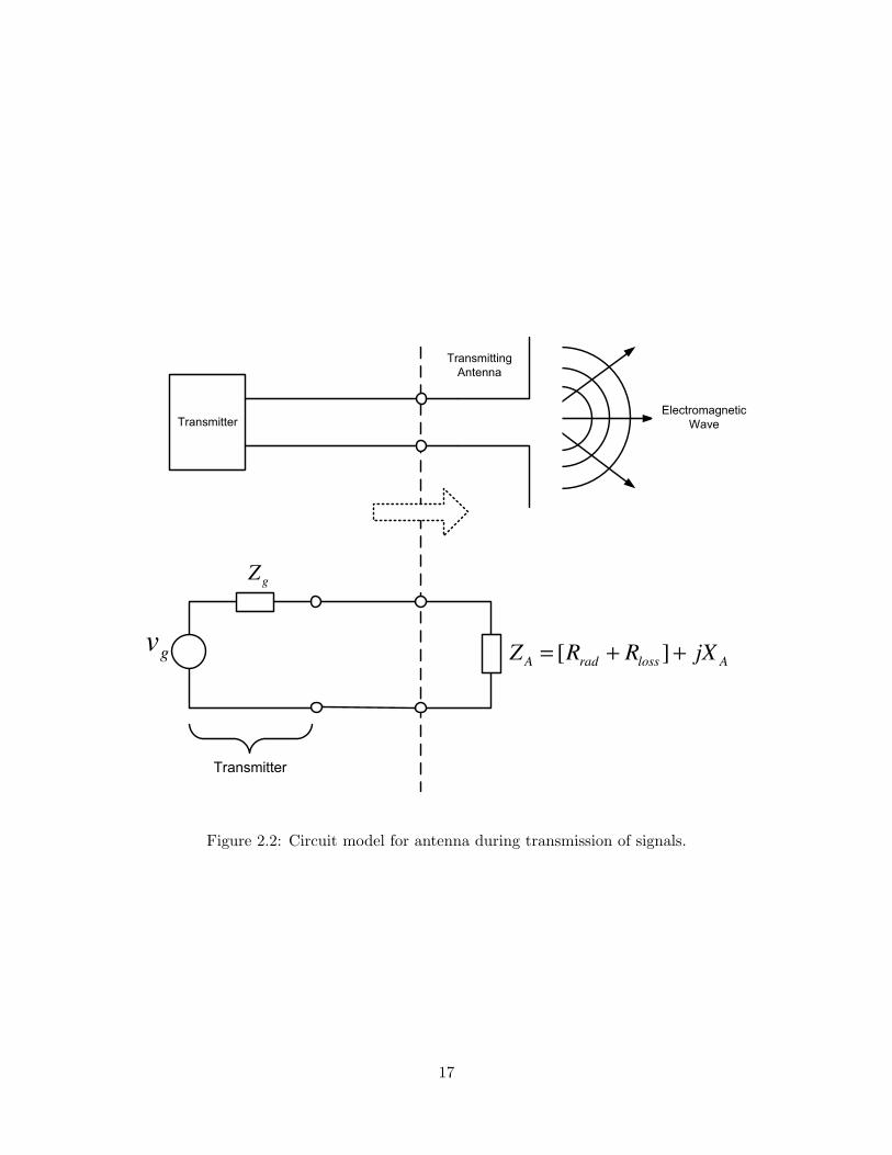
As shown in Figure 2.2, an antenna can be modeled as impedance ZA for transmission [23]. More-
over, in that figure the transmitter is modeled as a voltage source vg in series with the impedance
Zg. The antenna impedance ZA can be expressed as
ZA = RA + jXA (2.1)
where RA represents dissipation, which can be expressed as
RA = Rrad + Rloss (2.2)
where Rrad represents radiated power that leaves the antenna and never returns, and Rloss repre-
sents ohmic loss associated with finite conductivity. For the antennas of interest here, Rloss << Rrad
typically and can be neglected. The input reactance XA represents power stored in the near field
of the antenna; i.e. the non-radiating field.
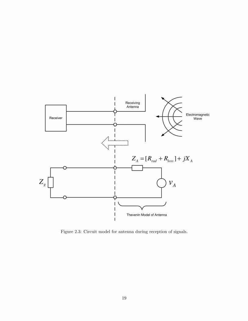
Figure 2.3 shows the Thevenin equivalent circuit model for an antenna in receive mode. Here, vA
is the open-circuit voltage, which is the voltage generated at the terminals of an open-circuited
antenna in response to an incident electric field, and Zg now represents the input impedance of the
receiver. As a consequence of reciprocity, the impedance of an antenna is identical during reception
16
TransmitterElectromagnetic
Wave
gv [ ]A rad loss AZ R R jX= + +
gZ
Transmitter
Transmitting
Antenna
Figure 2.2: Circuit model for antenna during transmission of signals.
17

and transmission.
The impedance ZA is the ratio of the voltage to current at the antenna terminals. For the purpose
of antenna–receiver integration, it is useful to know this parameter before starting to design an RF
front end. The impedance of a lossless short dipole, the length of which is very small compared to
its wavelength, can be represented as [23]
RA∼= Rrad ≈ 80π2
(h
λ
)2
Ω (2.3)
XA ≈ − 60π
(hλ
) [ln
(h
a
)− 1
]Ω (2.4)
where h is the half-length and a is the radius of the dipole. In this dissertation, our intention is
to pay special attention to the same type of simple straight monopole antennas which are already
very popular in hand–held and mobile transceivers. An ideal monopole antenna is obtained by
replacing one half of an ideal dipole antenna with an infinite ground plane. Due to the simple
relationship between the monopole and dipole, dipole impedance can easily be transformed to
monopole impedance using the relationship
ZA,monopole =12ZA,dipole. (2.5)
Various numerical methods, including the method of moments (MoM) and the finite difference time
domain (FDTD) method, are used to calculate antenna impedance for more complex or realistic
antennas for which simple expressions are not available. However, these methods provide only
numerical results (e.g., a list of impedance versus frequency), rather than an equivalent circuit of
the impedance of an antenna. For the purposes of RF front end design, however, the latter is
often more useful. Methods which produce circuit models for canonical antenna types (such as
dipoles) include [24–26]. We prefer the method of Tang, Tieng, and Gunn [25] due to its simplicity
and ability to accurately model the impedance of a dipole antenna over a broad bandwidth using
an equivalent circuit of just four components. This method will be referred to as “TTG” in this
dissertation. The TTG approach provides a circuit model for ZA of the form shown in Figure 2.4.
Equations 2.6 through 2.9 show the calculations for the values of the circuit elements. Note that
18
ReceiverElectromagnetic
Wave
Av
[ ]A rad loss AZ R R jX= + +
gZ
Thevenin Model of Antenna
Receiving
Antenna
Figure 2.3: Circuit model for antenna during reception of signals.
19

31C
32C
31L
31R
Figure 2.4: TTG circuit model for ZA for a dipole antenna.
the constants h and a are in meters, and the TTG model is only applicable for straight dipoles.
C31 =12.0674h
log(2h/a)− 0.7245pF (h in meters) (2.6)
C32 = 2h
0.89075
[log(2h/a)]0.8006 − 0.861− 0.02541
pF (h in meters) (2.7)
L31 = 0.2h
[1.4813 log(2h/a)]1.012 − 0.6188
µH (h in meters) (2.8)
R31 = 0.41288 [log(2h/a)]2 + 7.40754(2h/a)−0.02389 − 7.27408 kΩ (2.9)
2.3 Receiver System Design Parameters
This section briefly describes some useful system–level parameters of a receiver. This section is
organized as follows. Section 2.3.1 (“Digitization”) and Section 2.3.2 (“Sensitivity and Gain”)
describe digitization and the issues related to receiver’s sensitivity, respectively. In Section 2.3.3
(“Linearity”), various linearity parameters are defined. Finally, Section 2.3.4 (“Selectivity”) dis-
cusses selectivity.
2.3.1 Digitization
Digitization is the process of converting an analog signal into digital form. An analog to digital
converter (ADC) is used to perform this digitization. An ADC requires the magnitude of the input
20

signal in a particular range to digitize it properly. For example, most modern high–speed ADCs
output full scale when the input signal level is about 1 Vpp at 50Ω input impedance, i.e., at about
+3 dBm. It also has its own internal noise due to quantization, which is rounding error between
the analog input to the ADC and the output digitized value. The quantization noise of an ideal
ADC is
PQ = −1.76− 6.02Nb [dB relative to Pclip] (2.10)
where Nb is the number of bits of the ADC, and Pclip is the input power corresponding to the
maximum level the ADC can properly encode. However, due to the additional analog noise (ap-
proximately 2 dB typically) generated by the digitizer, a simpler and more realistic expression
is
PQ∼= −6Nb [dB relative to Pclip] (2.11)
The problem of determining the nominal gain and Nb for a particular receiver is now considered.
Let Pt be the total power input to the receiver at the antenna terminals. This power is the sum
of Pext (total external noise power received by the receiver), and PS (total power due to external
signal sources). The minimum required gain in the analog signal path, Gmin, and the maximum
allowed gain, Gr, are given by
Gmin =PQγq
Pext, and (2.12)
Gr =Pclipδr
Pt, (2.13)
respectively, where γq is the minimum desired ratio of external noise to quantization noise at the
input of the ADC, and δr is the maximum desired ratio of maximum acceptable input power to Pclip.
The ratio δr (typically about −10 dB) is chosen to accommodate temporary increases in power due
to intermittent signals and the spurious co-phasing of individual signals. Now, the quantization
noise power referenced to the input of the ADC is
PQ = Pclip10−6Nb/10. (2.14)
The ratio γq then given by
γq =PextGr
PQ=
Pext
Ptδr106Nb/10. (2.15)
21
It is desirable for external and internal noise to dominate over quantization noise. Thus γq is
typically chosen to be around 10. Solving for Nb yields [27]
Nb ≥ 1.67 log10
(Ptγq
Pextδr
). (2.16)
The number of bits required for quantization noise to be dominated by external noise by a factor
of γq at the output of the ADC can be calculated using Equation 2.16. In this process, Pext and
PS must be known, and γq and δr are design parameters.
2.3.2 Sensitivity and Gain
Sensitivity in a receiver can be defined as the minimum input signal power required to produce
a predetection (i.e., input to demodulator) output signal having a specified signal to noise ratio
(SNR). This input level is known as minimum detectable signal (MDS) and is given by
MDS = δkT0BF (2.17)
where δ is the minimum predetection SNR needed to detect a signal, k is Boltzmann’s constant
(1.38×10⁻²³ J/K), T0 is the noise reference temperature (290 K), and B is the detection bandwidth
of the receiver. F represents the noise figure of the receiver.
Noise figure is a characterization of the additional noise contribution of an RF stage and is defined
as the ratio of the SNR at the input of an RF stage to the SNR at the output of an RF stage; i.e.,
F =Si/Ni
So/No(2.18)
where Si and So is the signal at the input and output, respectively; and Ni and No is the noise at
the input and output, respectively.
Often in radio design, noise figure is specified, as opposed to minimizing or specifying MDS [28].
This approach makes it possible to overspecify the receiver’s noise figure during the design process.
This fact is especially true for the frequencies at VHF and below, where the receiver noise can
be dominated by the external environmental noise. An emphasis in the work reported in this
22
dissertation is to determine the extent to which this observation can be used to improve the usable
bandwidth of front ends. Chapter 4 describes this approach in more detail.
The purpose of gain (G) in a receiver is to increase the power of the received signal to a level
greater than that of the quantization noise of the ADC. However, gain which introduces excessive
additional noise defeats the purpose. In a well-designed receiver, environmental noise should dom-
inate over internal analog noise if possible; and quantization noise should be dominated by both
the environmental and internal analog noise. By combining these two conditions the receiver gain
requirement can be bounded as follows:
Pclipδr
Pt≥ G ≥
γqPclip10−0.6Nb
Pext. (2.19)
A traditional receiver design might proceed as follows: (1) We specify the sensitivity (MDS), which
then sets the receiver’s noise figure; (2) Nb is determined using Equation 2.16; and then (3) The
range of required total gain is calculated using Equation 2.19.
Another way to specify the sensitivity of receivers used for voice communication is audio signal–
to–noise–and–distortion ratio (SINAD). A typical specification for SINAD is that it must be at
least 12 dB for a 1 kHz audio tone [8]. The relationship between predetection SNR and SINAD is
described for analog FM in Appendix A. The analysis in the appendix shows that 12 dB SINAD
corresponds to 6.5 dB predetection SNR for a modulation bandwidth of 12.5 kHz and an audio
bandwidth of 3 kHz.
2.3.3 Linearity
Linearity is the desirable property that the output signal voltage (or current) varies in direct
proportion to the input signal voltage (or current), i.e., the output-to-input signal ratio is always
the same. Any practical analog system is only approximately linear, with the deviation from
linearity increasing with increasing power. Assuming that the input voltage signal applied to an
amplifier is vin, then the output voltage vout can be expressed as (weakly non–linear)
vout(t) = α0 + α1vin(t) + α2v2in(t) + α3v
3in(t) + . . . (2.20)
23

where αi is the ith order coefficient with i = 0, 1, 2, 3, .... The above equation describes a linear
system if αi ≡ 0 for i > 1.
An amplifier usually maintains approximately constant gain for low-level input signals. However,
at higher input levels, it goes into compression and the gain decreases. A graphical illustration of
this compression is shown in Figure 2.5. In other words, as the input signal increases in power, a
point is reached where the power of the signal at the output is not amplified by the same amount as
the smaller signal. At the point where the input signal is amplified by an amount 1 dB less than the
ideal gain, the 1 dB compression point (P1) has been reached. A common requirement is that input
power P1 should be greater than the largest expected input signal power. Using Equation 2.20, the
corresponding voltage can be expressed as [29]
√0.145
∣∣∣∣α1
α3
∣∣∣∣ (2.21)
This non–linear transfer function also leads to the generation of intermodulation products at the
output of the receiver. These intermodulation products can fall into the spectrum of interest
and interfere with the desired received signals. This is illustrated in Figure 2.6, in which for any
two tones at frequencies ω1 and ω2, the second-order intermodulation products (IM2s) appear
at frequencies ω1 ± ω2. Moreover, the third-order intermodulation products (IM3s) appear at
frequencies 2ω1 ± ω2 and ω1 ± 2ω2, respectively.
To characterize the non–linearity and the level of intermodulation products, there are two other
useful parameters: the second order intercept point (IP2), and the third order intercept point (IP3).
A graphical illustration of these parameters are also shown in Figure 2.5. The input–referred second-
order intercept point IIP2 is defined as the level of two equal-strength input tones at the point at
which the resulting IM2s have the same power as the input tones, as they appear in the output. The
input–referred third-order intercept point IIP3 is defined as the level of two equal-strength input
tones at the point at which the resulting IM3s have the same power as the input tones, as they
appear in the output. Using Equation 2.20, the voltage corresponding to IIP3 can be expressed
as [29] √43
∣∣∣∣α1
α3
∣∣∣∣. (2.22)
24

Input Power [dB]
Output Power [dB]
Nonlinear Response
Linear Response
1P
2IIP
3IIP
1 dB
Third Order Intermodulation
Slope = 3
Second Order Intermodulation
Slope = 2
Figure 2.5: Graphical explanation of P1, IIP2, and IIP3.
25

ω1ω
2ω 1
ω2
ω
1 22ω ω−
2 12ω ω−
2 1ω ω−
2 1ω ω+
22ω
12ω ω
Figure 2.6: Intermodulation products.
The relationship between P1 and IIP3 can be found by combining Equations 2.21 and 2.22 to yield
P1IIP3
≈ −9.6 dB. (2.23)
Typically, improvements in sensitivity and linearity are mutually exclusive. This can be demon-
strated using the simple example shown in Figure 2.7 consisting of three components: a preamplifier,
a variable attenuator, and a second amplifier. Note that in the figure OIP3 is the output third
order intercept point and noise figure of the attenuator is inverse to the attenuation. Total gain,
IIP3, and noise figure can be calculated using a stage–cascade gain, noise figure, and third order
intercept (GNI) analysis, described in Appendix B. Figure 2.8 shows the effect of total gain on
linearity (IIP3) and sensitivity (MDS). Note that improvement in MDS as attenuation is decreased
is accompanied by degradation in IIP3, and vice versa. Thus, it is difficult to achieve jointly opti-
mum MDS and IIP3. As a result, some trade–offs need to be made; e.g., to accept good sensitivity,
trading off linearity; or vice versa. This problem can be managed to some extent by incorporating
selectivity in the RF front end in order to suppress intermodulation products. This is discussed
next.
2.3.4 Selectivity
The selectivity of a receiver is defined as its ability to respond only to the desired frequency band and
reject unwanted frequencies including those likely to contribute to the intermodulation products.
Bandpass filters, filter banks, or tunable filters may be used to implement selectivity. Preselection
refers to the implementation of selectivity specifically in the RF front end of a receiver. Typically, for
26

Preamplifier Variable Attenuator Amplifier
Gain = +20 dB
OIP3 = 5 dB
F = 4 dB
Gain = variable
OIP3 = 20 dB
F = 1/ Gain
Gain = +30 dB
OIP3 = 10 dB
F = 8 dB
Figure 2.7: Simple receive system for linearity–sensitivity trade-off analysis.
0 5 10 15 20 25 30-120
-115
-110
-105
Attenuation [dB]
MD
S [ d
B(m
W/1
00kH
z)]
0 5 10 15 20 25 30-60
-50
-40
-30
-20
Attenuation [dB]
IIP
3 [dB
m]
Figure 2.8: Sensitivity (MDS) and IIP3 versus attenuator setting for the simple receiver modelshown in Figure 2.7
27

Filter 1
Filter 2
Filter N
Channel 1
Channel 2
Channel N
Input
Figure 2.9: N -channel multiplexer using bandpass filters.
single band radios operating over narrow fractional bandwidth, a single fixed or tunable bandpass
filter is adequate to perform preselection. However, it is often not possible to implement preselection
in a multiband radio or a radio which operates over large range of frequencies using a single bandpass
filter. A multiplexer can be a possible solution in this case. A multiplexer is a parallel or series
combination of filters to separate the RF input into multiple frequency bands. Figure 2.9 shows
an example of a multiplexer using parallel bandpass filters. An example of the implementation of
selectivity in superheterodyne receiver using a triplexer and bandpass filters is shown in Figure 1.3.
2.4 Receiver Architectures
This section describes some of the relevant architectures for receivers. Section 2.4.1 (“Superhetero-
dyne Architecture”) briefly discusses the widely-used superheterodyne architecture. Section 2.4.2
(“Direct Sampling Architecture”) describes direct sampling architecture, which can be the ideal
(but still not practical) receiver architecture for MMR. Finally, the direct conversion architecture
is discussed in Section 2.4.3 (“Direct Conversion Architecture”). Each section discusses the pros
and cons of the architectures for application to MMR.
28

2.4.1 Superheterodyne Architecture
A superheterodyne (also known as a “superhet”) receiver is a receiver in which the frequency
of the RF signal is mixed with a locally–generated “local oscillator” (LO) for conversion to an
intermediate frequency (IF). Superhet receivers have been in use for a long time and have been
quite popular since the early days of radio communication. One, two, or more stages of conversion
can be used in superhet architecture. Figure 2.10 provides a block diagram of a single–conversion
superhet receiver. The receiver consists of a preselector bandpass filter, a preamplifier, and a mixer
to convert the input RF frequency fRF to the IF frequency fIF . fLO is the frequency supplied by
the LO to the mixer.
This frequency conversion process also allows an undesired frequency called the “image frequency”
that is capable of producing the same IF that the desired input frequency produces. For example,
the image frequencies in Figure 2.10 would be fLO ± fRF depending on the side of signal injection
(If fLO > fRF then it is called high–side injection, and if fLO < fRF then it is called low–
side injection). This “image frequency” can be mixed with fLO, produce fIF , and can create
interference to proper reception of the signal. One of the major chores in the design of superhet
receivers is the suppression of unwanted image frequencies, which needs to be filtered out using an
image rejection filter preceding the mixer. Since this undesired signal is never filtered to “zero”
amplitude in practical receivers, usually designer does the frequency planning (to select the suitable
IF and LO frequencies) in such a way that the image frequencies do not fall into the desired band of
frequencies. However, the frequency planning becomes complicated and daunting for a receiver with
large tuning range, because it is difficult to avoid image frequencies inside the desired frequency
band.
There is a another problem which also limits the tuning range of a superhet receiver. This is due to
the interference of the “half–IF frequency”, which is located halfway between the frequencies of the
LO and the incoming RF signal. The half–IF signal is downconverted into the IF band by mixing
with the second harmonic of the LO signal [29, p.126]. Although this problem can be avoided with
adequate filtering in the front–end, or by using low–distortion amplifiers and mixers, it is hard to
mitigate adequately for MMR with large tuning ranges.
29
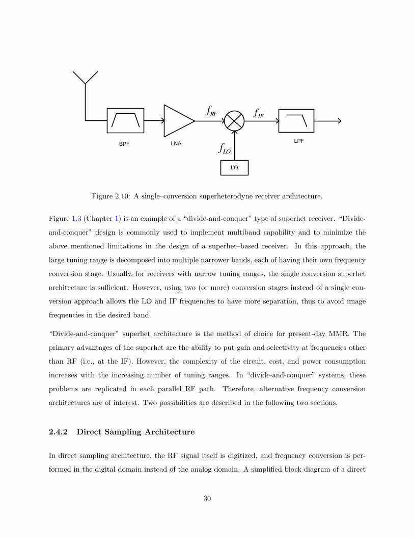
LPFBPF LNA
LO
RFf
LOf
IFf
Figure 2.10: A single–conversion superheterodyne receiver architecture.
Figure 1.3 (Chapter 1) is an example of a “divide-and-conquer” type of superhet receiver. “Divide-
and-conquer” design is commonly used to implement multiband capability and to minimize the
above mentioned limitations in the design of a superhet–based receiver. In this approach, the
large tuning range is decomposed into multiple narrower bands, each of having their own frequency
conversion stage. Usually, for receivers with narrow tuning ranges, the single conversion superhet
architecture is sufficient. However, using two (or more) conversion stages instead of a single con-
version approach allows the LO and IF frequencies to have more separation, thus to avoid image
frequencies in the desired band.
“Divide-and-conquer” superhet architecture is the method of choice for present-day MMR. The
primary advantages of the superhet are the ability to put gain and selectivity at frequencies other
than RF (i.e., at the IF). However, the complexity of the circuit, cost, and power consumption
increases with the increasing number of tuning ranges. In “divide-and-conquer” systems, these
problems are replicated in each parallel RF path. Therefore, alternative frequency conversion
architectures are of interest. Two possibilities are described in the following two sections.
2.4.2 Direct Sampling Architecture
In direct sampling architecture, the RF signal itself is digitized, and frequency conversion is per-
formed in the digital domain instead of the analog domain. A simplified block diagram of a direct
30

ADC
Figure 2.11: Block diagram of a direct sampling receiver.
sampling receiver is shown in Figure 2.11. The RF bandpass filter is used to select the desired band
and a preamplifier is used to amplify the signal to the input requirements of the ADC.
Digitization requires sample rate more than twice the highest bandwidth of interest. If it is needed
to design a MMR to operate in the frequency range of 100 MHz to 1 GHz using direct sampling, then
the required sampling speed for the ADC would be at least 2 GSPS (billion samples per second).
Achieving this is currently difficult, expensive, and power–intensive [30, 31]. As an example the
theoretical power consumption of a ADC operating at rates of 100s of MSPS is currently on the
order of watts. This is clearly a high value of power consumption for consideration to be included
in a mobile radio.
Even if high power consumption is acceptable, the RF design becomes a challenge due to the
linearity issues, especially for IM2s. Since direct sample architecture needs to pass the entire
tuning range, the IM2s are usually passed through the preamplifier and ADC, and thus corrupting
the desired signal. The only way to minimize this problem is to use narrowband filter, however, that
will limit the tuning range of the direct sampling receiver. In other words, the overall tuning range
of the direct sampling architecture is very much limited by the IM2s. From the above discussions
we can conclude that currently direct sampling may not be a generally–suitable architecture for
MMR.
2.4.3 Direct Conversion Architecture
In a direct conversion receiver (DCR), the incoming RF signal is directly mixed down to an analog
baseband signal with a center frequency of zero. A block diagram of a DCR is shown in Figure 2.12.
31

The RF signal is directly converted to complex baseband in-phase (I) and quadrature-phase (Q)
signals using a single LO set to the frequency to be received. The benefits of this architecture
include: elimination of IF stages; channel filtering and amplification are relatively easier at baseband
compared to at RF; reduced ADC requirements; power consumption reduction due to reduced
components and lower sampling rate; and wide tuning range, limited only by the initial BPF.
However, DCR has been in limited use in the past due to some major implementation drawbacks
compared to the superhet architecture [32, 33]. These include
1. DC Offsets
An incidental DC offset voltage is caused by self–mixing; the LO leakage actually mixes
with the original LO signal creating a DC voltage which can corrupt the signal of interest,
lowering the SNR, and more importantly, possibly saturating the baseband amplifier stages.
Figure 2.13 demonstrates the generation of DC offset and LO leakage in a DCR. Furthermore,
LO leakage through the RF sections is a large consideration in a design, since it can cause
in–band interference due to the proximity of the LO signal to the frequency of the incoming
RF. A similar effect occurs if a large interferer leaks from the preamplifier or mixer input to
the LO port and is multiplied by itself.
2. I/Q Imbalance
As shown in Figure 2.12, a DCR incorporates quadrature downconversion. It is difficult to
achieve constant amplitude and 90 phase over a large frequency range.
3. Phase Noise
As the down–converted RF signal is usually small in amplitude compared to the LO, and
nearly the same frequency, additional SNR degradation due to the phase noise of the LO is
often significant in DCR.
4. Even–Order Distortion
Non-linearities in the mixer and preamplifier produce even–order intermodulation, which
(especially second–order) introduces undesirable spectral components at baseband, and also
degrades the receiver sensitivity. Superhet receivers are susceptible primarily only to odd–
order intermodulation effects because even–order terms lie far outside the (narrow) tuning
32

LO
cos
sin
I
Q
Figure 2.12: Block diagram of a direct conversion receiver.
range (as shown in Figure 2.6). In direct conversion, on the other hand, the undesired
component due to even–order distortion can corrupt the down–converted signal of interest,
because two high frequency interferes can generate a low frequency even–order distortion
product which can pass through the mixers from the RF input to the baseband output.
Due to recent advancements in circuit implementation all of the problems can be alleviated to some
extent. These techniques are discussed briefly in the next section.
2.4.4 Modern Techniques to Overcome Direct Conversion Limitations
This section presents emerging techniques to solve the inherent limitations, discussed in the previous
section, of direct conversion architecture. Section 2.4.4.1 (“Chopper Stabilization”) presents a tech-
nique called chopper stabilization that reduces noise injected near DC, DC offset, and second–order
intermodulation products. Section 2.4.4.2 (“Differential Implementation”) discusses the advantages
of differential implementation of DCR.
2.4.4.1 Chopper Stabilization
Chopper stabilization (or “chopping”) [34], also known as “dynamic matching” [35], is an effective
method for mitigating in–band noise injected near DC, DC offset, and second–order intermodulation
products. Figure 2.14 illustrates the concept of chopping for an amplifier. Mixers are located at
33
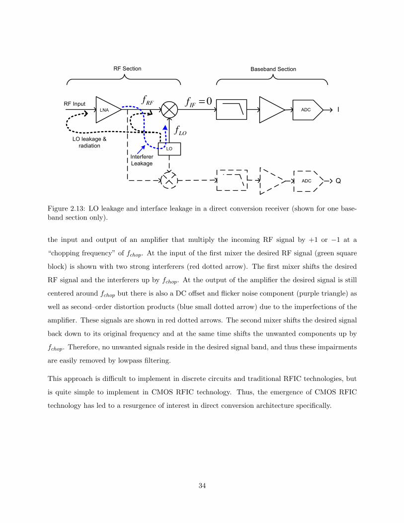
LO
RF Input
LO leakage &
radiation
LNA ADC
RF Section Baseband Section
Interferer
Leakage
RFf
LOf
0IFf =
ADC
I
Q
Figure 2.13: LO leakage and interface leakage in a direct conversion receiver (shown for one base-band section only).
the input and output of an amplifier that multiply the incoming RF signal by +1 or −1 at a
“chopping frequency” of fchop. At the input of the first mixer the desired RF signal (green square
block) is shown with two strong interferers (red dotted arrow). The first mixer shifts the desired
RF signal and the interferers up by fchop. At the output of the amplifier the desired signal is still
centered around fchop but there is also a DC offset and flicker noise component (purple triangle) as
well as second–order distortion products (blue small dotted arrow) due to the imperfections of the
amplifier. These signals are shown in red dotted arrows. The second mixer shifts the desired signal
back down to its original frequency and at the same time shifts the unwanted components up by
fchop. Therefore, no unwanted signals reside in the desired signal band, and thus these impairments
are easily removed by lowpass filtering.
This approach is difficult to implement in discrete circuits and traditional RFIC technologies, but
is quite simple to implement in CMOS RFIC technology. Thus, the emergence of CMOS RFIC
technology has led to a resurgence of interest in direct conversion architecture specifically.
34

+1/-1 @ fchop +1/-1 @ f
chop
fchop
fchop
Single-Ended RF
Input
Differential RF
Input
Input Switches Output Switches
fchop
fchopDesired
Signal
InterferersDC Offset
2nd Order
Distortion
Figure 2.14: Illustration of chopper stabilization technique.
2.4.4.2 Differential Implementation
Conventional (single ended) circuits use the voltage on a single conductor to convey the signal and
the voltage is measured with respect to ground. Differential circuits, in contrast, split the signal
across the two conductors in such a way that it can be defined as the voltage difference between
the conductors, and independent of the reference (ground) potential. Differential circuits provide
improvements in rejection of electromagnetic interference, increased common-mode signal rejection,
and increase in dynamic range rejection of even-order harmonic distortion [36]. The DC offset and
the even orders of intermodulation distortion can be reduced using differential implementation.
Thus, differential signaling can greatly improve the performance of a DCR.
To illustrate, let us assume that Vi1 and Vi2 are the input voltages to the differential RF block
shown in Figure 2.15. Since differential implementation requires equal magnitude and opposite
phase input signals, if Vi1 = A sin (ωt) then Vi2 = −Vi1 = −A sin (ωt). Now, using Equation 2.20,
the second–order non–linearity of the output voltage in the two output paths would be
V(2)o1 = α21V
2i1 = α21
A2
2(1− cos(2ωt)) (2.24)
35
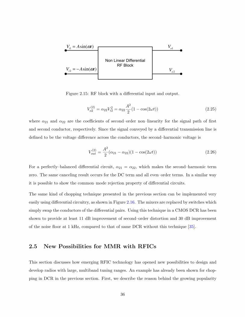
Non Linear Differential
RF Block
2sin( )iV A tω= −
1sin( )
iV A tω=
1oV
2oV
Figure 2.15: RF block with a differential input and output.
V(2)o2 = α22V
2i2 = α22
A2
2(1− cos(2ωt)) (2.25)
where α21 and α22 are the coefficients of second–order non–linearity for the signal path of first
and second conductor, respectively. Since the signal conveyed by a differential transmission line is
defined to be the voltage difference across the conductors, the second–harmonic voltage is
V(2)out =
A2
2(α21 − α22)(1− cos(2ωt)) (2.26)
For a perfectly–balanced differential circuit, α21 = α22, which makes the second–harmonic term
zero. The same canceling result occurs for the DC term and all even–order terms. In a similar way
it is possible to show the common–mode rejection property of differential circuits.
The same kind of chopping technique presented in the previous section can be implemented very
easily using differential circuitry, as shown in Figure 2.16. The mixers are replaced by switches which
simply swap the conductors of the differential pairs. Using this technique in a CMOS DCR has been
shown to provide at least 11 dB improvement of second–order distortion and 30 dB improvement
of the noise floor at 1 kHz, compared to that of same DCR without this technique [35].
2.5 New Possibilities for MMR with RFICs
This section discusses how emerging RFIC technology has opened new possibilities to design and
develop radios with large, multiband tuning ranges. An example has already been shown for chop-
ping in DCR in the previous section. First, we describe the reason behind the growing popularity
36

+1/-1 @ fchop +1/-1 @ f
chop
fchop
fchop
Single-Ended RF
Input
Differential RF
Input
Input Switches Output Switches
fchop
fchopDesired
Signal
InterferersDC Offset
2nd Order
Distortion
Figure 2.16: Illustration of differential implementation of the chopper stabilization technique.
of the CMOS process for RFICs. Then we present an example of a recent CMOS–based direct
conversion RFIC. We present some reasons why multiplexers become important to achieve MMR
using these RFICs.
CMOS is very popular in modern digital circuitry due to its high density, high speed, and inex-
pensive process. However, it is very difficult to implement RF circuity in CMOS due to process
variations and inaccurate design models [37]. In recent years, these problems have been greatly
mitigated. Since CMOS has the capability of implementing dense circuitry at reduced cost, multi-
ple transceivers can be implemented on a single chip, or multiple low–cost RFICs can be connected
in parallel for multiband operation. It is also possible to implement a lot of “tweaking parameters”
inside the RFIC to increase the performance of MMR. For example, these tweaking parameters
can be implemented as internal capacitors in series with internal switches. Fine adjustments in
filter responses is then possible by selecting capacitors to be added or removed as needed. Another
advantage is that the power consumption and cost of the MMR can be greatly reduced.
A few examples of recent work in this area includes an SDR receiver developed by Bagheri et. al.
in [38]. This is a 90 nm CMOS DCR operating in the 800 MHz to 5 GHz band with reconfigurable
bandwidth from 100 kHz to 8 MHz. Another transceiver RFIC, which is configurable from 700
MHz to 3.8 GHz for protocols with bandwidth of 25 kHz to 20 MHz, has been developed by
Bitwave Semiconductor in 130 nm CMOS [39]. This IC has only one receive and one transmit path.
Terocelo 1 has developed an RFIC for 500 MHz to 6 GHz in 65 nm CMOS. In 2007, Motorola
Research Laboratories developed a multiband direct conversion RFIC using 90 nm CMOS [40].1http://www.terocelo.com
37
Figure 2.17 shows the functional block diagram of this RFIC. A detailed description including a
performance analysis of this IC is presented in Chapter 7. This IC is designed for the operation
from 100 MHz to 2.5 GHz. Five receive paths and three transmit paths have been implemented in
the same IC. Since they share a common baseband section, only one receive and one transmit path
can be selected at a time. However, since the anticipated cost is so low (approximately $50 [41]),
it is possible to use multiple chips without much impact on MMR cost. Future chips with multiple
independent baseband sections are possible. The most recent versions of this IC have integrated
ADC/DAC. We use version 4 of this chip (as shown in Figure 2.17) to build a prototype MMR for
public safety application as described in Chapter 7.
Note that there are two categories of RFIC: Those with a single receive path, and those with
multiple receive paths. If we want to build a MMR using an RFIC having single receive path then
we require multiple RFICs to cover multiple bands. On the other hand, a single RFIC with multiple
receive paths itself might be sufficient for a MMR. Figure 2.18 shows two kinds of possible MMR
architectures using RFIC and a multiplexer. Figure 2.18(a) shows a “blocking” architecture in
which one single RFIC is used and each of its receive paths are connected to the multiple channels
of a multiplexer. This is the scheme that is possible with Motorola RFIC version 4, and which
is implemented in the prototype MMR in Chapter 7. On the other hand, Figure 2.18(b) shows
a “non-blocking” architecture in which multiple RFICs are connected to the multiple channels of
a multiplexer. The advantage of “non-blocking” architecture is that it is possible to receive or
transmit on multiple channels simultaneously.
From the above discussion it is clear that in order to get the advantage of these RFICs for MMR,
an RF front end is required which channelizes the incoming RF signal into separate bands (i.e.,
implementation of selectivity) for the receive paths of the RFIC. We prefer to use a multiplexer to
implement this RF front end.
2.6 Summary
This chapter presented a brief review of the various parts and parameters related to design of a
receiver. “Divide-and-conquer” superheterodyne architecture is favored to design MMR presently
38

Reference
PMA VGA BQ
PLL/VCO
SPI
MUX
Tx TEST POINTS
DCOC
Rx DDS
RX-1 IN
RX-2 IN
RX-3 IN
RX-4 IN
RX-5 IN
RX-BB OUT
TANKN
TANKPCP_PLL
FREF
CSEL
SPI_CLK
MOSI
MISO
RESET
Motorola Proprietary
++
++
++
Tx Reverse DDS
Cartesian BB Forward
Forward Pole 2 Butterworth Input Buffer
Reference
Tx Forward DDSReference
Cartesian Rev Amp/Mixer
TX-1 OUT
RX-FB-IN
TX-2 OUT
TX-3 OUT
TX-BB IN
Figure 2.17: Functional block diagram of the Motorola RFIC version 4 (used with permission, seeAppendix I).
39

RFIC
RFIC
RFIC
RFIC
BB
BB
BB
BB
RFIC
RFIC
RFIC
RFIC
BB
BB
BB
BB
(a) Blocking (b) Non-Blocking
Figure 2.18: Possible architectures to design a MMR using multiplexer and RFICs.
due to its ability to cover large tuning range with the necessary selectivity. However the com-
plexity, cost, and power requirements increase with increase in the number of desired frequency
bands. Direct conversion architecture is emerging as an alternative due to the advantages of small
form factor, low cost, reduced bill of materials, and low power consumption. Traditionally this
architecture is suffered from multiple number of implementation problems, however, most of which
can now be mitigated to a far greater extent due to the advancement of CMOS RFIC technology.
Moreover, the emergence of practical inexpensive CMOS RFICs, are motivating us to design a
MMR using these wideband direct conversion RFICs. However, in order to design a MMR using
a single traditional antenna, a new kind of RF front–end consisting of a multiplexer is needed for
the antenna–receiver integration. As a first step in identifying a suitable multiplexer design, the
next section describes the fundamental limits of antenna–receiver matching and also discusses some
traditional techniques to achieve wideband matching.
40
Chapter 3
Antenna–Receiver Interfacing
Wideband impedance matching (i.e., matching over large fractional bandwidths) is made difficult
by the fundamental limitations of impedance matching. This chapter reviews these limitations
as well as various wideband matching techniques and their limitations. This chapter is organized
as follows. Section 3.1 (“Antenna Matching & Parameters”) describes some basic parameters of
matching. Fundamental limitations of matching are reviewed in Section 3.2 (“Fundamental Limi-
tations”). Section 3.3 (“Wideband Matching using Passive Components”) summarizes techniques
for wideband matching using passive components. Section 3.4 (“Antenna Tuning using Variable
Reactors”) reviews some current research trends in antenna matching using variable reactors. In
Section 3.5 (“Non-Foster Impedance Matching”), a wideband matching technique using active com-
ponents is briefly described. This chapter is summarized in Section 2.6 (“Summary”).
3.1 Antenna Matching & Parameters
Usually, receivers are designed assuming frequency–independent input impedance of standard real
value (e.g., 50Ω), shown as ZL in Figure 3.1. However, over wide tuning ranges the antenna
impedance ZA is frequently quite different from ZL and it varies significantly with frequency, as
shown in Figure 1.4. An impedance–matching network is used to manage the impedance mismatch
between the antenna and the receiver as shown in Figure 3.1.
41

Impedance
Matching
NetworkTransceiver
Antenna
Transmission
Line
0Z
0Z
AZ in
Z
Impedance
Matching
Network
Rest of
Receiver
Antenna
AZ L
Z
Figure 3.1: General configuration for antenna matching.
Usually, the impedance–matching network is designed to provide the maximum power transfer.
From this perspective, the ideal impedance–matching network has three requirements: (1) input
impedance should be the conjugate of the antenna impedance, i.e., Z∗A, (2) the network should be
lossless, i.e., no ohmic elements (especially resistors) should be present in the matching circuit, and
(3) the output impedance should be Z∗L, i.e., real-valued. A matching circuit having these three
properties will result in all available power (i.e., what the antenna can generate into a conjugate
matched load) being delivered to the rest of the receiver. The question of how good the matching
actually needs to be depends on the requirements of the application.
Antenna–receiver impedance–matching is commonly narrowband in nature (i.e., bandwidth is 10%
or less). For example, a design is optimized for the center frequency, but the result works well
enough over a small band of frequencies around the design frequency. The match can be perfect
at the center frequency, but degrades away from it. However, wideband matching is needed for
the MMR applications identified in Chapter 1, since these operate over large fractional bandwidths
possibly using a single antenna. The ability to achieve an acceptable match over a bandwidth of
10% or more is fundamentally limited by a bound on the product of gain and bandwidth. Section 3.2
(“Fundamental Limitations”) discusses this in more detail.
The impedance match between an antenna and the receiver can be characterized in terms of voltage
standing wave ratio (VSWR), defined as
ρ =1 + |Γ|1− |Γ|
, (3.1)
42
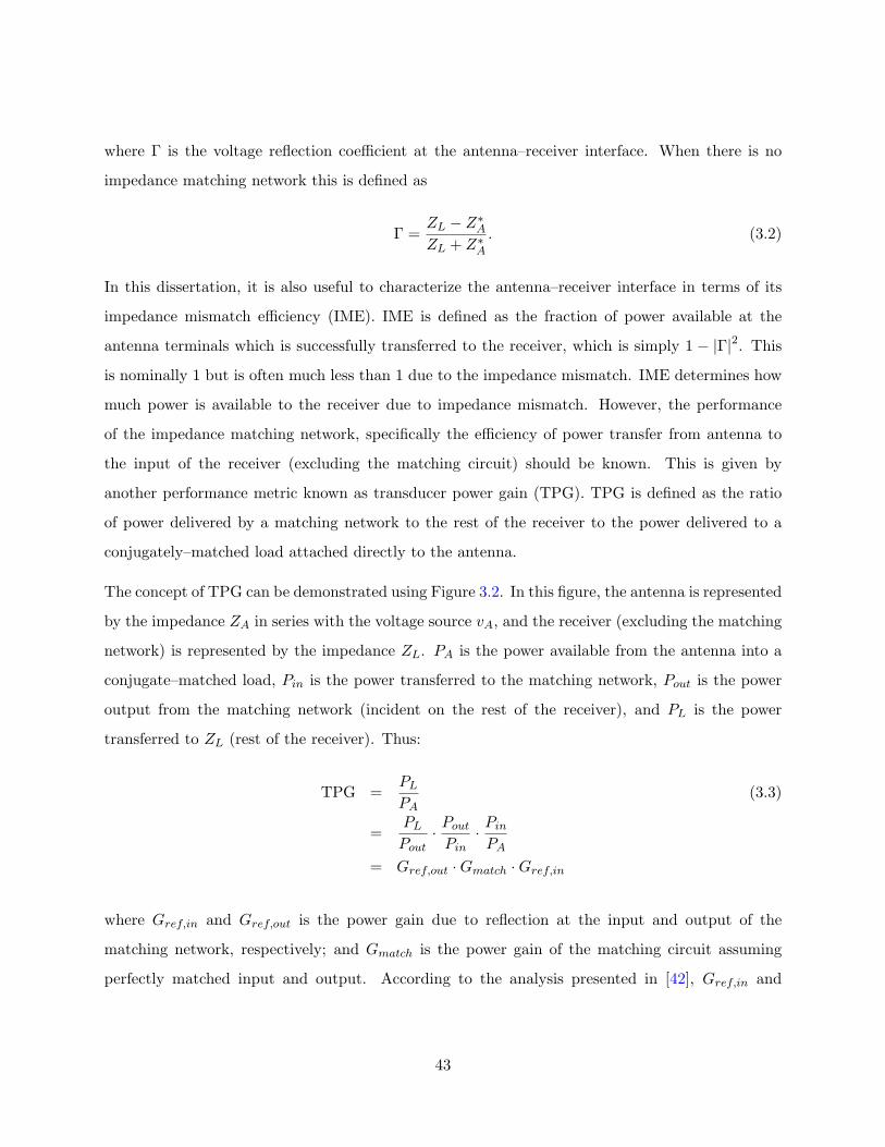
where Γ is the voltage reflection coefficient at the antenna–receiver interface. When there is no
impedance matching network this is defined as
Γ =ZL − Z∗
A
ZL + Z∗A
. (3.2)
In this dissertation, it is also useful to characterize the antenna–receiver interface in terms of its
impedance mismatch efficiency (IME). IME is defined as the fraction of power available at the
antenna terminals which is successfully transferred to the receiver, which is simply 1 − |Γ|2. This
is nominally 1 but is often much less than 1 due to the impedance mismatch. IME determines how
much power is available to the receiver due to impedance mismatch. However, the performance
of the impedance matching network, specifically the efficiency of power transfer from antenna to
the input of the receiver (excluding the matching circuit) should be known. This is given by
another performance metric known as transducer power gain (TPG). TPG is defined as the ratio
of power delivered by a matching network to the rest of the receiver to the power delivered to a
conjugately–matched load attached directly to the antenna.
The concept of TPG can be demonstrated using Figure 3.2. In this figure, the antenna is represented
by the impedance ZA in series with the voltage source vA, and the receiver (excluding the matching
network) is represented by the impedance ZL. PA is the power available from the antenna into a
conjugate–matched load, Pin is the power transferred to the matching network, Pout is the power
output from the matching network (incident on the rest of the receiver), and PL is the power
transferred to ZL (rest of the receiver). Thus:
TPG =PL
PA(3.3)
=PL
Pout· Pout
Pin· Pin
PA
= Gref,out ·Gmatch ·Gref,in
where Gref,in and Gref,out is the power gain due to reflection at the input and output of the
matching network, respectively; and Gmatch is the power gain of the matching circuit assuming
perfectly matched input and output. According to the analysis presented in [42], Gref,in and
43

AZ
+-
Av
Two Port Matching
Network LZ
AΓ inΓ
LΓoutΓ
inZ
,ref inG
matchG ,ref outG
AP inPout
PLP
SZ
+- Sv
LZ
SΓLΓ
0Z
SR
SX
LR
LX
outZ
Figure 3.2: Block diagram to calculate transducer power gain.
Gref,out are
Gref,in =1− |Γin|2
|1− ΓAΓin|2, (3.4)
Gref,out =1− |ΓL|2
|1− ΓoutΓL|2, (3.5)
where ΓA, Γin, Γout, and ΓL are the voltage reflection coefficients indicated in Figure 3.2. Also:
ΓA = Γ∗in =ZA − Z∗
in
ZA + Z∗in
, (3.6)
ΓL = Γ∗out =ZL − Z∗
out
ZL + Z∗out
, (3.7)
where Zin and Zout are the input and output impedance of the matching network indicated in
Figure 3.2. Substitution of Equations 3.4 and 3.5 into 3.3 yields:
TPG =1− |Γin|2
|1− ΓAΓin|2Gmatch
1− |ΓL|2
|1− ΓoutΓL|2. (3.8)
As a special case, if input and output of the matching network is completely matched with the
44

impedance of the source and load, respectively, then the value of all the reflection coefficients
would be zero and we have TPG = Gmatch.
3.2 Fundamental Limitations
Matching may be difficult, so it is important to know the actual requirements, and it is also useful to
know the fundamental limits, so that we can get the idea about how reasonable our matching goal
or requirement is. This section presents some of the fundamental limitations of antenna matching.
3.2.1 Bode–Fano Limit
It is not always possible to get unity TPG even if there is no loss in the matching circuit, due to
the trade-off between the bandwidth of a matching circuit and the TPG through that matching
circuit. This trade-off has been described by Bode and Fano [43, 44]. They primarily presented
a systematic study of the origin and nature of the theoretical limitations on the tolerance and
bandwidth of match and of their dependence on the characteristics of the given load impedance.
The basic idea of their work is: while the operating bandwidth at the input to the matching circuit
increases as a function of the number of tuning circuits, there is an upper limit to the bandwidth
that can be realized. The first investigation related to this fundamental limit was made by Bode
for the case of an impedance ZL consisting of a resistance R in parallel with a capacitance C, and
he showed that in this case the fundamental limitation takes the form [44]
∫ +∞
−∞ln
∣∣∣∣ 1Γ(ω)
∣∣∣∣ dω ≤ π
RC(Parallel RC). (3.9)
Let us assume the voltage reflection coefficient Γ(ω) is constrained to be unity outside the frequency
range ωL to ωH and Γ(ω) is constrained to be constant in ωL to ωH , as shown in Figure 3.3. Then,
Equation 3.9 can be solved for the minimum reflection coefficient
Γmin = exp(− π
Bω0RC
)(Parallel RC) (3.10)
45

where ω0 ≡√
ωHωL and B = (ωH − ωL)/(ωHωL). This reflection function, which is illustrated in
Figure 3.3, can be fit exactly using a polynomial of infinite degree, corresponding to a matching
network having infinite number of elements. As a result the above reflection value of |Γmin| can be
achieved only with a matching network having infinite number of circuit elements. The following
are two insights that can be gained from Equations 3.9 and 3.10:
1. To obtain the best possible match over the widest bandwidth, the reflection coefficient should
be equal to one outside of the passband, as this allows for |Γ| to be minimized inside the
passband.
2. If the bandwidth needs to be increased, this can be done only by decreasing the TPG, i.e.,
increasing |Γ|) through the matching circuit.
The above result is specific to parallel RC impedances, whereas we are interested to know the
fundamental limitations of matching for antenna–receiver integration generally. In general this is
quite difficult, however there are approximations relevant to a few more special cases. For example,
the impedance of an electrically–short antenna can be approximated by a series RC or series RL
circuit. The following equations show the Bode–Fano bounds for the series RC and series RL
impedances [45] ∫ +∞
−∞ω−2 ln
∣∣∣∣ 1Γ(ω)
∣∣∣∣ dω ≤ πRC (Series RC) (3.11)
∫ +∞
−∞ω ln
∣∣∣∣ 1Γ(ω)
∣∣∣∣ dω ≤ πR
L(Series RL) (3.12)
and the resulting Γmin’s assuming Γ(ω) is the form of Figure 3.3 are
Γmin = exp(−πRCω0
B
)(Series RC) (3.13)
Γmin = exp(− πR
Lω0B
)(Series RL). (3.14)
Although these bounds are useful to know the maximum achievable bandwidth given a TPG con-
straint, in reality it is not reasonable to specify a matching circuit with an infinite number of circuit
components. Fano obtained a modified version of the relationship presented above (Equation 3.9)
46
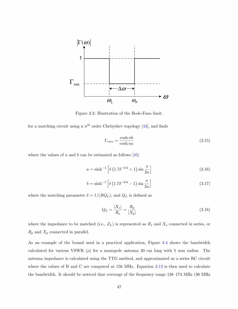
ω
( )ωΓ
1
minΓ
Lω Hω
ω∆
Figure 3.3: Illustration of the Bode-Fano limit.
for a matching circuit using a nth order Chebyshev topology [43], and finds
Γmin =coshnb
coshna(3.15)
where the values of a and b can be estimated as follows [45]
a = sinh−1[δ(1.7δ−0.6 + 1
)sin
π
2n
](3.16)
b = sinh−1[δ(1.7δ−0.6 − 1
)sin
π
2n
](3.17)
where the matching parameter δ = 1/(BQL), and QL is defined as
QL =|Xs|Rs
=Rp
|Xp|(3.18)
where the impedance to be matched (i.e., ZL) is represented as Rs and Xs connected in series, or
Rp and Xp connected in parallel.
As an example of the bound used in a practical application, Figure 3.4 shows the bandwidth
calculated for various VSWR (ρ) for a monopole antenna 20 cm long with 5 mm radius. The
antenna impedance is calculated using the TTG method, and approximated as a series RC circuit
where the values of R and C are computed at 156 MHz. Equation 3.13 is then used to calculate
the bandwidth. It should be noticed that coverage of the frequency range 138–174 MHz (36 MHz
47

bandwidth around 156 MHz a public safety band) can be achieved only for ρ ≥ 7, and that better
VSWR is possible only by reducing the bandwidth.
3.2.2 Foster’s Reactance Theorem
Foster’s Reactance Theorem [46] states that the first derivative of the reactance of a passive loss-
less circuit with respect to frequency is always positive. This is obvious for single inductors and
capacitors, as shown in the following equations
XL(ω) = jωL ;∂
∂ω(XL(ω)) = jL > 0 (3.19)
XC(ω) =−j
ωC;
∂
∂ω(XC(ω)) =
j
ω2C> 0 (3.20)
This gives additional insight as to why broadband matching is very difficult using only passive
reactances. This can be demonstrated using an example. If it is desired to perfectly match the
antenna impedance shown in Figure 1.4 to a purely resistive input impedance of a receiver then it
is needed to use a matching circuit which exactly cancels the antenna reactance over the desired
bandwidth. Over the frequency range where the slope is positive (including resonance), the cor-
responding ideal matching circuit’s input reactance has a negative slope, and therefore cannot be
achieved using only passive lossless reactive components, such as capacitors and inductors. While
it is possible for the matching circuit to cancel the reactance exactly at one frequency, it is not
possible to cancel the reactance exactly over a range of frequencies.
An attempt to sidestep this limitation is Non–Foster Matching, discussed in Section 3.5.
3.3 Wideband Matching using Passive Components
This section reviews some existing wideband matching techniques using fixed–value passive com-
ponents. Section 3.3.1 (“Analytical Techniques”) discusses some classical analytical techniques and
their limitations, whereas Section 3.3.2 (“Real Frequency Technique”) presents a popular iterative
technique. The model used is as shown in Figure 3.5, which shows an antenna of known impedance
ZA(f) = RA(f) + jXA(f) connected to a receiver modeled as a matching network in cascade with
48

100 110 120 130 140 150 160 170 180 190 2000
10
20
30
40
50
60
70
80
90
Frequency [MHz]
Bandw
idth
[M
Hz]
ρ = 1.5
ρ = 2
ρ = 7
Figure 3.4: Matching bandwidth for various VSWR estimated using an approximate form of theBode–Fano bound for a monopole antenna 20 cm long with 5 mm radius.
49

+AZ
LRiv
-
+-Av LR
AZ ov
+
-
*
Matching Circuit
+
1( )R j Cω
−
−
LRiv
-
+-Av ov
+
-
Lossless
Matching
Circuit
Series RC Impedance
( )ωΓ
( )LZ f+-g
vLossless
Matching
Network
gR
( )mZ f
( )AZ f
+-A
vLossless
Matching
NetworkLR
( )mZ f
Figure 3.5: Configuration to demonstrate the matching techniques.
a resistive load RL.
3.3.1 Analytical Techniques
An example of a classical broadband matching technique using passive reactances is discussed
in [47]. The first step is to define how good the match should be at the center frequency, i.e.
selecting the value of ρ (input VSWR). Subsequent steps are most easily explained in terms of the
Smith Chart. A constant ρ (VSWR) circle and impedance curve are drawn. The next step is to
add reactance (L or C, series or parallel) in such as a way that the impedance at mid–frequency
is shifted towards the constant VSWR circle as much as possible. The second network element is
selected to position the mid-frequency impedance to accept the maximum permissible VSWR, and
the remaining two elements are selected to “wrap” or shift the end portions of the impedance curve
(i.e. impedance at the high and low frequencies in the desired bandwidth) to within the desired
VSWR circle. Thus the first two elements set the efficiency of the match, and the last two elements
determine the bandwidth.
Demonstrating this method, Figure 3.6 shows a four–element matching circuit to match a monopole
antenna 1.97 m long and 21 mm diameter (This antenna to be used in field experiments in Chap-
ter 4) to a 50Ω load over the frequency range 10–28 MHz. This design assumes the simulated
impedance of the antenna shown in Figure 4.15. To find out the Bode–Fano limit, the antenna is
modeled as a series RC impedance, the values (R = 4.9Ω and C = 32.0 pF) of which are calculated
50

from the antenna impedance at the geometric mean frequency (i.e., 16.7 MHz) of this frequency
range. According to the approximate Bode–Fano limit, the maximum theoretical TPG is then –10.4
dB, which is calculated using Equation 3.13 with TPG (in dB) = 10 log10(1− |Γmin|2). Figure 3.7
shows the TPG achieved by the designed four–element network. This matching circuit clearly
performs well around 19 MHz but quickly degrades at higher and lower frequencies. Although
the match could be improved by adding more components to the circuit, the design process using
this graphical method will become intractable. As is, this matching circuit provides about 5 MHz
bandwidth for –10.4 dB minimum TPG.
Other approaches allow matching circuits of higher order, but are based on assumptions about the
source impedance; e.g., requiring certain network topologies such as series RC or parallel RL. An
example is a method described by Rhea [48, 49]. He describes a matching technique that begins
with a Chebyshev filter with constant (e.g. 50Ω) termination impedance and modifies it. This
method is only applicable to antenna impedance which can be modeled as series RC or parallel
RL. In this method the reactive part of the impedance of the antenna is absorbed in the filter
reactance, i.e., the reactance of the component (in the filter) which is close to the antenna needs
to be changed in such a way that the combination of the antenna reactance and the new value of
this component’s reactance are equal to the original value of this reactance. The procedure is as
follows: First, a Chebyshev filter for which the input and output impedances are both equal to
the load impedance is designed for the desired band of frequencies. Then the value of absorption
reactance can be found from
Cseries =B
2πgRAfc(Series RC) (3.21)
Lshunt =B ×RA
2πgfc(Parallel RL) (3.22)
where fc is the geometric center frequency, B is the fractional bandwidth, g is the value of the Cheby-
shev lowpass prototype element (component value of the prototype with termination impedance
1Ω) adjacent to the source [50], RA is the source resistance, Cseries is the minimum series capac-
itor value which can be absorbed, and Lshunt is the minimum shunt inductor value which can be
absorbed.
51
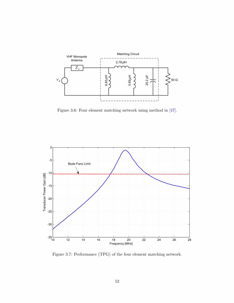
Av Ω50
6.83 H
2.78 H
0.69 H
25.2 pF
VHF Monopole
Antenna
Matching Circuit
AZ
µ
µµ
Figure 3.6: Four element matching network using method in [47].
10 12 14 16 18 20 22 24 26 28-35
-30
-25
-20
-15
-10
-5
0
Frequency [MHz]
Tra
nsducer
Pow
er
Gain
[dB
]
Bode-Fano Limit
Figure 3.7: Performance (TPG) of the four element matching network.
52
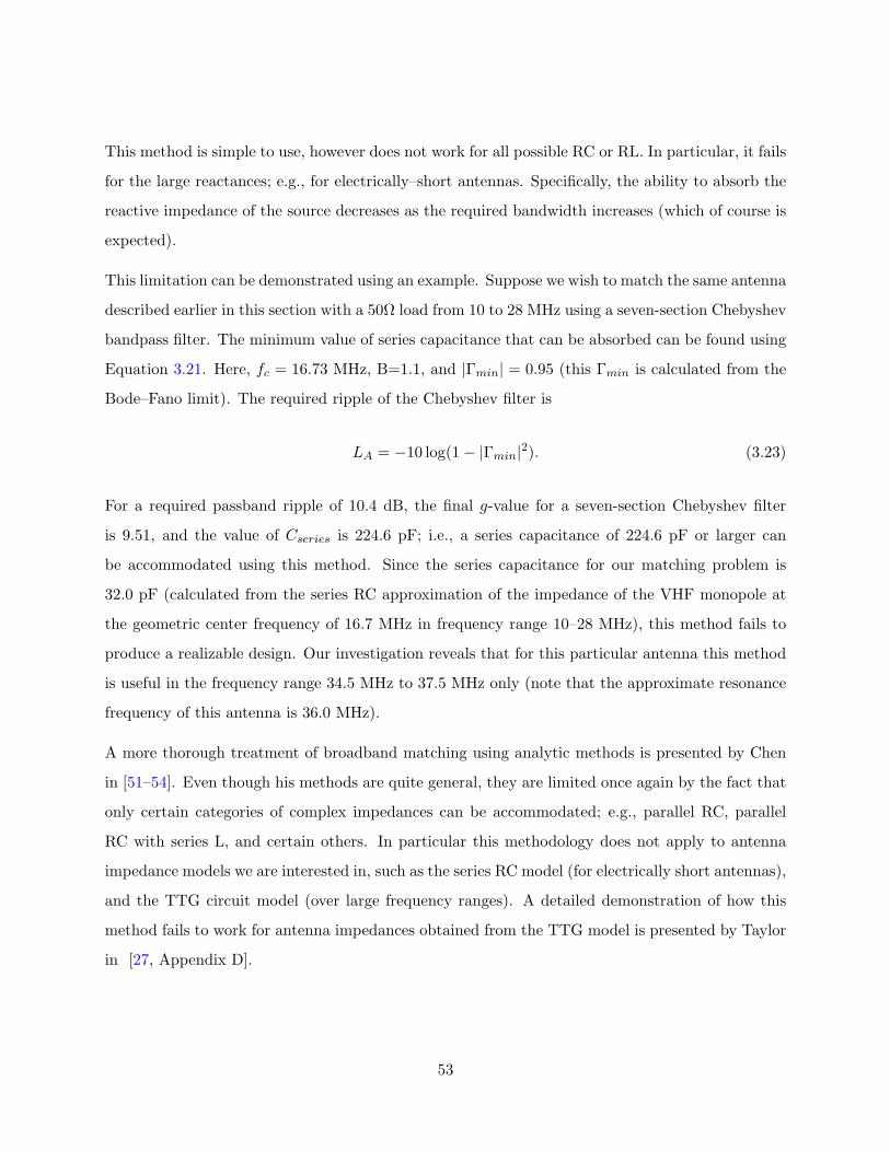
This method is simple to use, however does not work for all possible RC or RL. In particular, it fails
for the large reactances; e.g., for electrically–short antennas. Specifically, the ability to absorb the
reactive impedance of the source decreases as the required bandwidth increases (which of course is
expected).
This limitation can be demonstrated using an example. Suppose we wish to match the same antenna
described earlier in this section with a 50Ω load from 10 to 28 MHz using a seven-section Chebyshev
bandpass filter. The minimum value of series capacitance that can be absorbed can be found using
Equation 3.21. Here, fc = 16.73 MHz, B=1.1, and |Γmin| = 0.95 (this Γmin is calculated from the
Bode–Fano limit). The required ripple of the Chebyshev filter is
LA = −10 log(1− |Γmin|2). (3.23)
For a required passband ripple of 10.4 dB, the final g-value for a seven-section Chebyshev filter
is 9.51, and the value of Cseries is 224.6 pF; i.e., a series capacitance of 224.6 pF or larger can
be accommodated using this method. Since the series capacitance for our matching problem is
32.0 pF (calculated from the series RC approximation of the impedance of the VHF monopole at
the geometric center frequency of 16.7 MHz in frequency range 10–28 MHz), this method fails to
produce a realizable design. Our investigation reveals that for this particular antenna this method
is useful in the frequency range 34.5 MHz to 37.5 MHz only (note that the approximate resonance
frequency of this antenna is 36.0 MHz).
A more thorough treatment of broadband matching using analytic methods is presented by Chen
in [51–54]. Even though his methods are quite general, they are limited once again by the fact that
only certain categories of complex impedances can be accommodated; e.g., parallel RC, parallel
RC with series L, and certain others. In particular this methodology does not apply to antenna
impedance models we are interested in, such as the series RC model (for electrically short antennas),
and the TTG circuit model (over large frequency ranges). A detailed demonstration of how this
method fails to work for antenna impedances obtained from the TTG model is presented by Taylor
in [27, Appendix D].
53
3.3.2 Real Frequency Technique
Having demonstrated the limitations of closed form analytical techniques, we now consider a popular
iterative numerical technique. In [55, 56], Carlin introduces a method called the Real Frequency
Technique (RFT) to achieve broadband matching of an antenna having arbitrary impedance to a
resistive load. An important advantage of this method with respect to methods based on circuit
models is its capability to work with experimental (i.e., measured) impedance data. For this reason,
this technique is advantageous for matching impedances not easily expressible in forms of circuit
models, such as antennas. The RFT method consists of the following two steps to find out and
realize the impedance Zm(f) = Rm(f) + jXm(f) of the matching circuit shown in Figure 3.5:
1. Optimization of Zm(f)
The purpose of the optimization step is to find a realizable Zm(f) that optimizes TPG over
the desired frequency range. To begin, RA(f) is approximated by a number of straight
line segments, i.e., in a piecewise linear fashion, with frequency break points at 0 < f0 <
f1 . . . < fn corresponding to the available impedance data values. Once this is done, RA(f)
is entirely specified in terms of the slopes of the line segments, which may now be viewed as
unknown parameters for the optimization problem. The next step is to find the slopes which
optimize TPG at the frequency break points. Once the line segments describing Rm(f) have
been found, the corresponding reactance function Xm(f) can be determined from the Hilbert
transform [57, Sec. 3.4].
2. Realization of Zm(f)
After finding Zm(f), the next step is to find a lossless LC network that has this impedance.
The process starts by constructing Rm(f), an approximation to the original piecewise linear
Rm(f) in the form of a rational polynomial, employing the methods suggested by Carlin
and Yarman in [56]. Next step is to convert Rm(f) to Zm(s), a rational polynomial, where
s = jω is the complex frequency, using the Gerwetz procedure [45]. The final step is the
interpretation of Zm(s) as a lossless LC network terminated in RL using the Darlington
synthesis procedure [57].
54

Yarman [58] improved this technique, eliminating the numerical evaluation of the Hilbert transfor-
mation to improve the computational efficiency. The main idea of his modification is the generation
of the unit–normalized scattering parameters S11, S12, S21, and S22 of the lossless matching circuit
from the unknown – but initialized – numerator polynomial h(p) of the unit–normalized reflection
coefficient S11 = h(p)/g(p). The term g(p) is the Hurwitz polynomial and can be calculated from
h(p). The unknown real coefficients h0, h1, h2, . . . , hn of h(p) are determined using a nonlinear op-
timization routine such that TPG is maximized over a specified pass band. The matching network
can then be realized as a lossless network with resistive termination and synthesized using long
division from these optimized scattering parameters.
Figure 3.8 shows the matching circuit designed using this version of RFT (known as simplified
RFT) to match the same antenna described earlier to a 50Ω load for 10–28 MHz. The performance
of this circuit is presented in Figure 3.9. This matching circuit is designed using the MATLAB code
supplied in [59] using the simulated impedance data shown in Figure 4.15. Note that this matching
circuit provides much more uniform performance over the desired frequency range. In this case
14.4 MHz bandwidth is achieved for –10.4 dB minimum TPG. The improvement in performance
compared to the four–element technique (Figure 3.7) is significant, but comes at the expense of a
greater number of matching sections.
Although the RFT method seems very attractive to solve the wideband matching problem, it is very
complicated to implement. Optimization is an inherent part of this technique, and it is generally
unconstrained and multidimensional in nature. Although there are other techniques available to
perform this optimization [60], there is no guarantee that the optimization will converge, or converge
to the global optimum.
3.4 Antenna Tuning using Variable Reactors
When the achievable bandwidth–TPG trade–off is insufficient for an application, the use of variable
reactances may be considered to increase the range of frequencies over which a TPG requirement
can be met. Figure 3.10 shows the concept of antenna-receiver interfacing using variable reactors.
By changing the impedance of reactors we can achieve good impedance matching at at least one
55
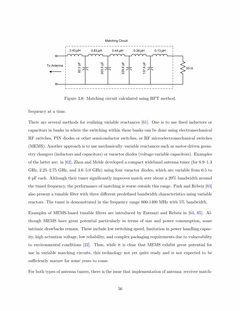
Ω50
2.43 H
To Antenna
0.83 H 0.44 H 0.38 H 0.13 H
82.2 pF
203.5 pF
229.6 pF
137.6 pF
Matching Circuit
µ µ µ µ µ
Figure 3.8: Matching circuit calculated using RFT method.
frequency at a time.
There are several methods for realizing variable reactances [61]. One is to use fixed inductors or
capacitors in banks in where the switching within these banks can be done using electromechanical
RF switches, PIN diodes or other semiconductor switches, or RF microelectromechanical switches
(MEMS). Another approach is to use mechanically–variable reactances such as motor-driven geom-
etry changers (inductors and capacitors) or varactor diodes (voltage-variable capacitors). Examples
of the latter are: in [62], Zhou and Melde developed a compact wideband antenna tuner (for 0.9–1.3
GHz, 2.25–2.75 GHz, and 3.6–5.0 GHz) using four varactor diodes, which are variable from 0.5 to
6 pF each. Although their tuner significantly improves match over about a 20% bandwidth around
the tuned frequency, the performance of matching is worse outside this range. Park and Rebeiz [63]
also present a tunable filter with three different predefined bandwidth characteristics using variable
reactors. The tuner is demonstrated in the frequency range 800-1400 MHz with 5% bandwidth.
Examples of MEMS-based tunable filters are introduced by Entesari and Rebeiz in [64, 65]. Al-
though MEMS have great potential particularly in terms of size and power consumption, some
intrinsic drawbacks remain. These include low switching speed, limitation in power handling capac-
ity, high actuation voltage, low reliability, and complex packaging requirements due to vulnerability
to environmental conditions [22]. Thus, while it is clear that MEMS exhibit great potential for
use in variable matching circuits, this technology not yet quite ready and is not expected to be
sufficiently mature for some years to come.
For both types of antenna tuners, there is the issue that implementation of antenna–receiver match-
56
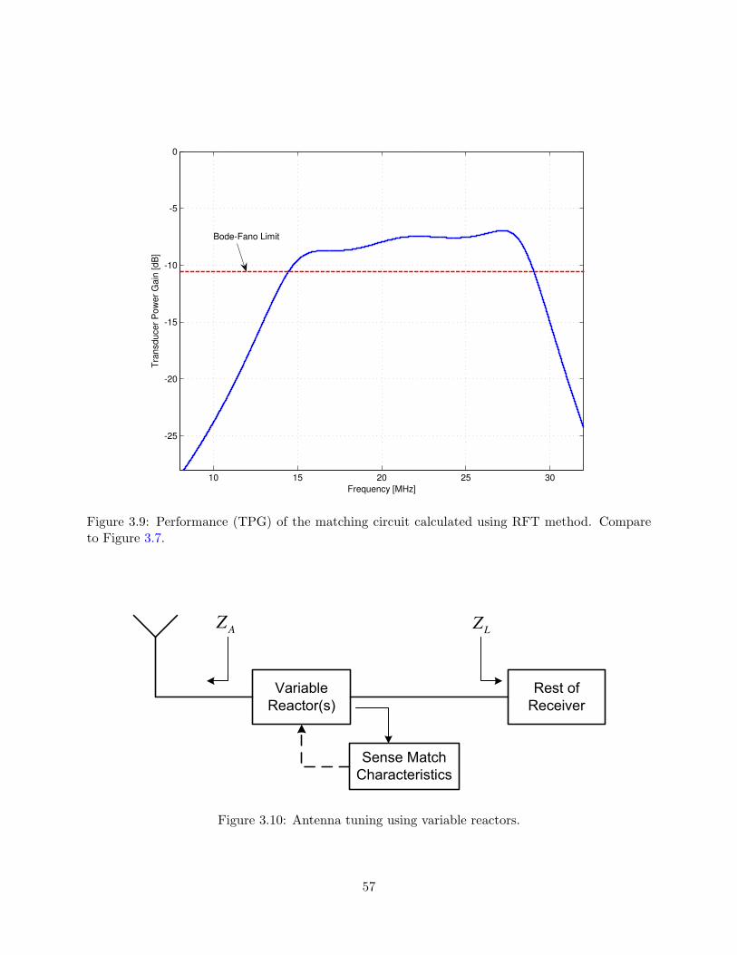
10 15 20 25 30
-25
-20
-15
-10
-5
0
Frequency [MHz]
Tra
nsducer
Pow
er
Gain
[dB
]
Bode-Fano Limit
Figure 3.9: Performance (TPG) of the matching circuit calculated using RFT method. Compareto Figure 3.7.
Variable
Reactor(s)
Rest of
Receiver
Sense Match
Characteristics
AZ
LZ
Figure 3.10: Antenna tuning using variable reactors.
57
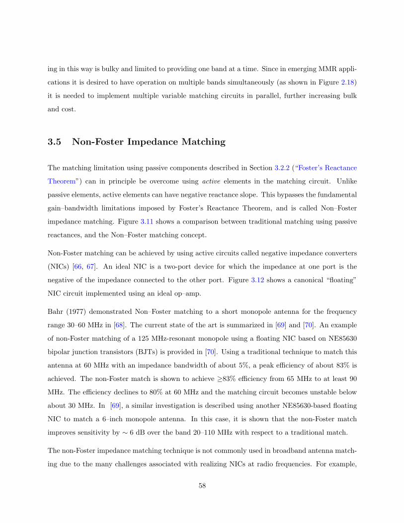
ing in this way is bulky and limited to providing one band at a time. Since in emerging MMR appli-
cations it is desired to have operation on multiple bands simultaneously (as shown in Figure 2.18)
it is needed to implement multiple variable matching circuits in parallel, further increasing bulk
and cost.
3.5 Non-Foster Impedance Matching
The matching limitation using passive components described in Section 3.2.2 (“Foster’s Reactance
Theorem”) can in principle be overcome using active elements in the matching circuit. Unlike
passive elements, active elements can have negative reactance slope. This bypasses the fundamental
gain–bandwidth limitations imposed by Foster’s Reactance Theorem, and is called Non–Foster
impedance matching. Figure 3.11 shows a comparison between traditional matching using passive
reactances, and the Non–Foster matching concept.
Non-Foster matching can be achieved by using active circuits called negative impedance converters
(NICs) [66, 67]. An ideal NIC is a two-port device for which the impedance at one port is the
negative of the impedance connected to the other port. Figure 3.12 shows a canonical “floating”
NIC circuit implemented using an ideal op–amp.
Bahr (1977) demonstrated Non–Foster matching to a short monopole antenna for the frequency
range 30–60 MHz in [68]. The current state of the art is summarized in [69] and [70]. An example
of non-Foster matching of a 125 MHz-resonant monopole using a floating NIC based on NE85630
bipolar junction transistors (BJTs) is provided in [70]. Using a traditional technique to match this
antenna at 60 MHz with an impedance bandwidth of about 5%, a peak efficiency of about 83% is
achieved. The non-Foster match is shown to achieve ≥83% efficiency from 65 MHz to at least 90
MHz. The efficiency declines to 80% at 60 MHz and the matching circuit becomes unstable below
about 30 MHz. In [69], a similar investigation is described using another NE85630-based floating
NIC to match a 6–inch monopole antenna. In this case, it is shown that the non-Foster match
improves sensitivity by ∼ 6 dB over the band 20–110 MHz with respect to a traditional match.
The non-Foster impedance matching technique is not commonly used in broadband antenna match-
ing due to the many challenges associated with realizing NICs at radio frequencies. For example,
58
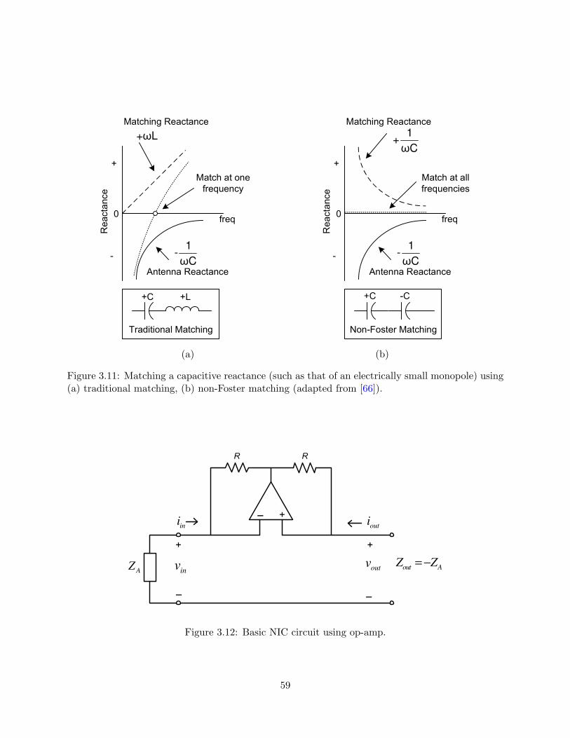
1-ωC
+ωL
Reactance
+
-
0
Matching Reactance
Antenna Reactance
Match at one
frequency
Traditional Matching
freq
1-ωC
1+ωC
Reactance
+
-
0
Matching Reactance
Antenna Reactance
Match at all
frequencies
Non-Foster Matching
freq
+L+C +C -C
1-ωC
+ωL
Reactance
+
-
0
Matching Reactance
Antenna Reactance
Match at one
frequency
Traditional Matching
freq
1-ωC
1+ωC
Reactance
+
-
0
Matching Reactance
Antenna Reactance
Match at all
frequencies
Non-Foster Matching
freq
+L+C +C -C
(a) (b)
Figure 3.11: Matching a capacitive reactance (such as that of an electrically small monopole) using(a) traditional matching, (b) non-Foster matching (adapted from [66]).
_+
R R
AZ out AZ Z= −inv outv
+ +
_ _
ini outi
Figure 3.12: Basic NIC circuit using op-amp.
59

since a NIC depends on shifting the phase of an incoming signal by 180, any parasitic phase
difference between the signals will prevent a perfect negative impedance conversion. Also, load
impedance significantly affects the operation (especially the stability) of the circuit [71]. Since it
uses active circuitry with frequency–variable input impedance, it suffers from stability, linearity,
and noise issues. In general, it is not mature enough to apply into MMR application. However, it
might be an attractive future work to extend the research presented here.
3.6 Summary
Wideband matching of an antenna to a receiver is very difficult in MMR due to the fundamental
limitations of the Bode–Fano bound and Foster’s Reactance Theorem. In this chapter, several
matching techniques as well as their limitations have been discussed using examples in which a
VHF monopole antenna (1.97 m long and 21 mm diameter) is matched to a 50Ω load over the
frequency range 10–28 MHz. A matching circuit (consisting of four passive components), which is
designed using a classical method achieved 5 MHz bandwidth at the TPG calculated from Bode–
Fano limit (–10.4 dB). Although the matching bandwidth can be increased using more components
in the matching circuit, the design becomes intractable with the increase of components using
classical methods. A higher order match can be achieved using RFT, an iterative technique which
does not require the antenna impedance in circuit form. RFT provides 14.4 MHz bandwidth at
-10.4 dB TPG to match the above antenna. However, the implementation of RFT is complex
and depends heavily on optimization, which might not converge and is nevertheless still bound by
fundamental limits. Antenna tuning is limited to providing a match for only one narrow band at
a time. Non–Foster matching is another alternative, but suffers from stability, linearity, and noise
issues. In summary, none of these approaches is entirely satisfactory for the purposes of MMR as
laid out in Chapter 1. In the next chapter, we will consider an alternative approach which bypasses
fundamental limitations of antenna matching in a different way.
60
Chapter 4
Sensitivity-Constrained Front-End
Design
Wideband matching is fundamentally limited by the Bode–Fano limit and Foster’s reactance the-
orem presented in the previous chapter. Hence antenna–receiver integration is very difficult, espe-
cially for a receiver covering a large range of frequencies. However, if a receiver is already external
noise–dominated then further improvement of antenna–receiver matching does not necessarily im-
prove the overall sensitivity. Presently there is no simple standard way to take this into account
when specifying matching and noise figure requirements of receivers, especially with large, multi-
band tuning ranges.
This chapter describes the effect of external noise on matching and sensitivity. This chapter is
organized as follows. Section 4.1 (“Noise Characterization”) describes the various external sources
of noise and Section 4.2 (“Optimum Noise Figure Specification”) describes an “optimum noise
figure” specification for multiband receivers based on the findings. Section 4.3 (“Implications
for Design of Antenna Matching”) describes some antenna matching implications due to external
noise. In Section 4.4 (“Experimental Verification”), a field experiment is performed to verify the
theoretical developments of the previous sections. Finally, Section 4.5 (“Summary”) summarizes
this chapter.
61
4.1 Noise Characterization
The sensitivity of a receiver is related to signal to noise ratio, which in turn depends on noise.
In order to build a sensitivity-constrained front-end we need to account for the effect of noise
in our front-end design. Section 4.1.1 (“Sources of Noise”) describes common noise sources and
Section 4.1.2 (“Noise Modeling”) presents noise modeling. Finally, Section 4.1.3 (“Characterization
of Environmental Noise”) discusses how these noise sources can be characterized to obtain the
parameters to be used in the noise model.
4.1.1 Sources of Noise
Primarily two kinds of noise sources are present in any RF front end: Internal noise, which is
generated by electrical components internal to the system; and external noise, which comes from
the environment. This section briefly discusses these two noise sources.
An important source of internal noise is Johnson noise (also known as “thermal noise”), which is
associated with ohmic losses in an antenna or in electronic components of a radio system. This is
generated by the thermal agitation of the electrons inside electrical circuits. Shot noise and flicker
noise are also examples of internal noise.
External noise sources may be classified as (1) natural, such as noise from the atmosphere, from
the Sun and the planets, Galactic noise generated by astrophysical processes [72], noise due to the
radiation of cosmic microwave background (CMB), and thermal noise from the Earth itself; and (2)
anthropogenic, i.e., from industrial and other man–made activities. The external noise delivered
to a receiver includes natural noise plus additional noise resulting from human activity. These
contributions have been measured and characterized in considerable detail, and are conveniently
described in a report by the International Telecommunication Union (ITU) [73]. Figure 4.1 shows
the power spectral density (PSD) of various external noise environments calculated using the models
provided in [73]. Noise due to the CMB contributes about 2.7 K to the antenna temperature. On the
other hand, among the terrestrial noise sources, the ground generally radiates a noise temperature
of roughly equal to ambient temperature (about 290 K), part of which is received by the antenna.
Atmospheric noise is caused by natural atmospheric processes, primarily due to lightning discharges
62

10-1
100
101
102
103
-180
-170
-160
-150
-140
-130
-120
-110
-100
-90
-80
Frequency [MHz]
Pow
er
Spectr
al D
ensity [dB
m/R
BW
], R
BW
=1H
z
Business A
Residential
Rural
Quiet Rural
Galactic
Business B
Figure 4.1: PSD of various noise environments calculated using the data provided in [73].
in thunderstorms. Depending on location man–made noise is categorized as “Business A”, “Business
B”, “Residential”, “Rural”, and “Quiet rural” in [73]. The characterization of these noise sources
will be addressed in greater detail in Section 4.1.3.
4.1.2 Noise Modeling
Johnson noise generated in a resistor can be modeled as a voltage source, representing the noise
of the non-ideal resistor, in series with an ideal noise–free resistor. The root mean square (RMS)
magnitude of the noise voltage due to Johnson noise is given by
vn =√
4kT∆fR (4.1)
where k is Boltzmann’s constant (1.38× 10⁻²³ J/K), T is the physical temperature of resistor, ∆f
is bandwidth, and R is the resistance of the ideal resistor. The voltage induced at the terminals of
63

Antenna immersed
in external noise
AT
*
AZ
L AP kT f= ∆
L AP kT f= ∆
AZ
+
-
External Noise Model
,A nv%
4 A AkT fR= ∆
*
AZ
Figure 4.2: Modeling external noise of an antenna immersed in external noise temperature TA.
an antenna by external noise can be modeled in the same manner as internal noise; i.e., as a voltage
source in series with an impedance. Figure 4.2 shows the concept of modeling environmental noise
delivered by an antenna immersed in external noise at noise temperature TA. In the figure, vA,n
and ZA represent the noise voltage and antenna impedance respectively, PL represents the power
transfer assuming a perfectly matched load, and RA is real part of the antenna impedance ZA.
Since later sections of this chapter require knowledge of external noise, the next section describes
this characterization of environmental noise sources in detail.
4.1.3 Characterization of Environmental Noise
The median noise figure values for any of the external noise models described in [73] is given by
F = c− d log10 f [dB] (4.2)
where f is the frequency in MHz, and c and d are given in Table 4.1. Figure 4.3 shows the median
noise figure of these environmental noise sources. It should be noted that the values of c and d
provided in Table 4.1 is only valid in the frequency range of 0.3 to 250 MHz for all environmental
noise sources with some exceptions, such as the “Quiet Rural” model is valid from 0.3 to 30 MHz,
the Galactic background model is valid from 10 to 250 MHz, and the “Business B” model is valid
from 200 to 900 MHz.
64

Table 4.1: Median values for noise model parameters [73].
Environment Category c d
Business A 76.8 27.7Business B 44.3 12.3Residential 72.5 27.7Rural 67.2 27.7Quiet Rural 53.6 28.6Galactic Noise 52.0 23.0
In our research we are interested to know how much PSD is contributed by external noise to the
input of a RF front end, to determine whether the front–end is external noise dominated or not.
It is convenient to use noise temperature for the calculation of PSD instead of noise figure. Hence
we would like to transform this characterization to a more convenient form expressed in noise
temperature. From Equation 4.2 we see that external noise can be accurately described in terms of
a mean noise temperature TA following the power law af−b. This also can be expressed in terms of
Gaussian statistics with a variance σ2 with respect to location within a given noise environment.
Table 4.2 presents a modified version Table 4.1, including the values of a and b. In Table 4.2,
‘Celestial’ refers to the combination of Galactic noise and the CMB. In [73], ‘Business A” is used
in 0.3 to 250 MHz and ‘Business B” is used in 200 to 900 MHz. In the new characterization, these
are merged into a single model which is similar to ‘Business A” below 130 MHz and similar to
‘Business B” below 900 MHz. This modification is done simply extending the “Business B” curve
below 200 MHz to find the intercept point with “Business A”. Figure 4.4 shows the new median
noise figures using Table 4.2.
The statistical variation of mean noise power with respect to location is expressed in terms of “decile
variations”, Du and Dl, the upper and lower decile values (i.e., the values exceeded 10 percent and
90 percent of the time) of the variability of noise power. The decile values are not only dependent
on frequency, but also upon the actual location in various noise sources environment. Assuming
that the noise distribution is symmetric about the mean, Du is approximately equal to Dl. The
values of Du and Dl are provided in [73]. We can find the standard deviation σ, i.e., the square
root of variance with respect to location, of noise from the given decile values. The area under the
65

10-1
100
101
102
103
-10
0
10
20
30
40
50
60
70
80
90
Frequency [MHz]
Media
n N
ois
e F
igure
[dB
] (r
ef. tem
p. 290
o K
)
Business A
Business B
Residential
Rural
Quiet Rural
Galactic
Figure 4.3: Median noise figures for various external noise sources using the model provided in [73].
66
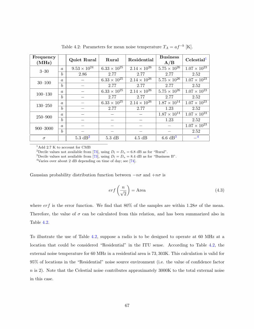
Table 4.2: Parameters for mean noise temperature TA = af−b [K].
FrequencyQuiet Rural Rural Residential
BusinessCelestial1
(MHz) A/B
3–30a 9.53× 1024 6.33× 1025 2.14× 1026 5.75× 1026 1.07× 10²³
b 2.86 2.77 2.77 2.77 2.52
30–100a − 6.33× 1025 2.14× 1026 5.75× 1026 1.07× 10²³
b − 2.77 2.77 2.77 2.52
100–130a − 6.33× 1025 2.14× 1026 5.75× 1026 1.07× 10²³
b − 2.77 2.77 2.77 2.52
130–250a − 6.33× 1025 2.14× 1026 1.87× 10¹⁴ 1.07× 10²³
b − 2.77 2.77 1.23 2.52
250–900a − − − 1.87× 10¹⁴ 1.07× 10²³
b − − − 1.23 2.52
900–3000a − − − − 1.07× 10²³
b − − − − 2.52σ 5.3 dB2 5.3 dB 4.5 dB 6.6 dB3 −4
1Add 2.7 K to account for CMB2Decile values not available from [73], using Dl = Du = 6.8 dB as for “Rural”.3Decile values not available from [73], using Dl = Du = 8.4 dB as for “Business B”.4Varies over about 2 dB depending on time of day; see [74].
Gaussian probability distribution function between −nσ and +nσ is
erf
(n√2
)= Area (4.3)
where erf is the error function. We find that 80% of the samples are within 1.28σ of the mean.
Therefore, the value of σ can be calculated from this relation, and has been summarized also in
Table 4.2.
To illustrate the use of Table 4.2, suppose a radio is to be designed to operate at 60 MHz at a
location that could be considered “Residential” in the ITU sense. According to Table 4.2, the
external noise temperature for 60 MHz in a residential area is 73, 303K. This calculation is valid for
95% of locations in the “Residential” noise source environment (i.e. the value of confidence factor
n is 2). Note that the Celestial noise contributes approximately 3000K to the total external noise
in this case.
67

100
101
102
103
104
-40
-20
0
20
40
60
80
Frequency [MHz]
Media
n N
ois
e F
igure
[dB
] (r
ef. tem
p. 290
o K
)
Business
Residential
Rural
Quiet Rural
Galactic
Figure 4.4: Median noise figures for various external noise sources using the model presented inTable 4.2.
68

4.2 Optimum Noise Figure Specification
This section presents and demonstrates a specification and a methodology to find out the “opti-
mum” noise figure for a receiver. This is not a traditional optimum point. A receiver’s sensitivity
depends on the total noise of the receiver, which includes the noise generated internally and the
noise received from the environment. Usually sensitivity increases with the improvement of the
internal noise figure of a receiver. However, when a receiver is external noise–dominated, then after
a certain threshold further improvement of the receiver’s internal noise figure does not necessarily
improve the sensitivity significantly. Rather, it complicates the circuit design, and thus increases
the total design cost. This subjective point at which further improvements in noise figure do not
significantly improve sensitivity, but only increases complexity, is what we refer to as the “opti-
mum” point. This concept is particularly useful for receivers with large, multiband tuning ranges.
The value in this specification is that it (1) prevents the designer from over–specifying the receiver
noise figure and (2) can be exploited in our proposed work as a loosened constraint in the sense that
we can tolerate a poor–quality match where we are safely external noise-dominated, or in other
situations where the best possible noise figure is not required or desired.
Let us assume that an antenna is connected to a preamplifier, which can be described in terms of
its input impedance Zp, gain Gp, and noise temperature Tp. Now the PSD due to the external
noise temperature TA at the output of the preamplifier, referenced to the input of the preamplifier,
is given by
Sext = ηkTA
[1− |Γ|2
]Gp (4.4)
where η is the antenna efficiency associated with the loss due to the finite conductivity of the
materials used to make the antenna and absorption by the imperfect (nonperfectly-conducting)
ground, and Γ = (Zp − Z∗A)/(Zp + Z∗
A). The preamplifier–generated noise at the output of the
receiver can be expressed in terms of the preamplifier’s input–referenced noise temperature Tp as
Np = kTpGp (4.5)
69
Now the total PSD at the output of receiver can be expressed as
Sout = Sext + Np (4.6)
= (ηTA
[1− |Γ|2
]+ Tp)kGp
The ratio γ of external noise to internally–generated noise at the input of the receiver is thus
γ =Sext
Np
= ηTA
Tp
[1− |Γ|2
](4.7)
The optimal preamplifier temperature Tp is that which is sufficiently small to make Sext dominant
over Np. This can be achieved by γ on the order of 10 or so. However, smaller γ – perhaps even
γ < 1 – might be appropriate depending on the application and the need to trade off sensitivity
for improved linearity or reduced cost. For example (and as shown in Figures 2.7 and 2.8), if we
decrease Tp (i.e., improve sensitivity) then it reduces linearity. The corresponding noise factor is
computed from noise temperature using
Fopt =Topt
T0+ 1 (4.8)
where
Topt = ηTA
γ
[1− |Γ|2
](4.9)
is the optimal value of Tp, and T0 is the reference noise temperature (290 K).
To illustrate the concept, an example is presented here for the frequency range of 3 MHz to 3
GHz. For receiver noise figure specification purposes, one should choose the applicable category of
man-made noise, determine the associated noise temperature, and subtract from this some margin
n representing the confidence with which the designer wishes to be sure this value is not exceeded.
n is conveniently described in units σ. Figure 4.5 shows the optimum noise figure 10 log10(Fopt)
for γ = 10 and n = 2σ in various environments assuming η[1− |Γ|2
]= 1 (i.e., perfectly matched
antenna with no ground loss). The specification shown in Figure 4.5 is the linear sum of celestial
noise plus that of the most relevant man-made noise category, reduced by the specified margin.
70

107
108
109
0
10
20
30
40
50
60
Frequency (Hz)
Nois
e F
igure
(dB
)
Quiet Rural
Rural
Residential
Business
Galactic+CMB
Figure 4.5: Example of the optimum noise figure specification. Lines with markers show themaximum noise figure for which the sensitivity of a receiver is limited by the noise generated by itsown front end (by a factor of 10 over external noise) in 95% of locations that can be classified as theindicated type. The irreducible mean contribution from the combination of Galactic backgroundnoise and the CMB is also shown.
For example, if a receiver is required to operate at 200 MHz in a “Business” environment, then
according to the specification the noise figure should be 6 dB in order to ensure sensitivity is
dominated by external noise by a factor of 10 over 95% of locations.
It should be noted that the specification described here does not take into account individual sources
of radio frequency interference and impulsive noise; these are separate considerations. Also, the
values in Table 4.2 are based on the measurements reported in [73], which may not be universally
valid or representative of new sources of man-made noise. However, we can easily modify this table
employing some corrective measures such as increasing n, or making site-specific measurements and
extracting from them applicable values of a and b. It can also be modified using noise measurements
71

reported by others. Some examples follow. Rogers et. al. presented external noise measurements
from 70 to 1500 MHz in suburban and rural environments of Northeast [75]. In [76], Wagstaff and
Merricks presented measurements of man–made noise from 100 MHz to 3 GHz with bandwidths
up to 10 MHz. Gorka et. al. presented some man–made noise measurements for the medium wave
band based on measurements performed in Spain and Mexico [77]. Note that the measurements
reported in [73] also do not contain any information about indoor noise sources. It is also possible
to change/modify our noise specification incorporating indoor noise sources if it is known.
4.3 Implications for Design of Antenna Matching5
In the previous section we demonstrated that the optimum noise figure for a receiver is not nec-
essarily the minimum possible noise figure. Thus, the best possible match between antenna and
receiver is not necessarily the one which maximizes TPG. We now wish to know how good the match
must be to get reasonable noise figure. As we know from the previous section, if an RF front–end
is strongly dominated by external noise; then any additional improvement in match would not
significantly improve sensitivity.
Figure 4.6 shows the contributions to the PSD at the preamplifier output for a lossless antenna
(η = 1) for several fixed values of ρ, assuming preamplifier gain Gp = +22 dB and noise temperature
288.6 K (i.e., noise figure F = 3.0 dB). The ρ = 1 curve corresponds to a perfectly–matched
condition for all frequencies (for illustration purposes only, perfect matching at all frequencies is
not practically feasible) and impedance mismatching increases with the increasing values of ρ. This
plot provided some insight for understanding how good matching must be at any given frequency
to obtain Galactic noise–limited operation. Note that below 100 MHz, a preamplifier with a very
modest noise figure (i.e., noise temperature on the order of a few hundred degrees Kelvin) can be
sufficient to obtain a very large γ even if the antenna is badly matched. Note also that the highest
Galactic noise–limited frequency is determined by the noise figure of the preamplifier. For example,
Figure 4.6 illustrates that even for ρ = 10 the front–end is externally noise dominated up to about
80 MHz for a preamplifier with 3 dB noise figure.5This is an extension of an analysis originally presented in [78].
72

107
108
-150
-140
-130
-120
-110
-100
-90
-80
Frequency [MHz]
PS
D a
t pre
am
p o
utp
ut [d
Bm
/RB
W], R
BW
=1kH
z
ρ = 1
ρ = 10
ρ = 100
Preamplifier
Galactic noise at indicated VSWR
Figure 4.6: Contributions to the PSD at the preamplifier output for a lossless antenna (η = 1) byGalactic noise. In this plot, preamplifier gain and noise figure are chosen to be Gp = +22 dB andF = 3.0 dB, respectively.
73

Since Galactic noise is unavoidable, it is the worst case scenario for receiver design. As shown in
Figure 4.4, radios are often used in areas where the noise PSD is much greater than the PSD of
Galactic noise. Figure 4.7 repeats Figure 4.6, but now assuming “Residential” noise. As we can see
the frequency range over which internal noise is dominated by external noise is greatly increased.
This frequency range of noise–limited operation is further increased for even noisier environments,
such as “Business”.
In summary, a receiver can be external noise–dominated even for a large mismatch between the
antenna and preamplifier, depending on noise environment and frequency. An important caveat
is that the parameters of a preamplifier ( Zp, Gp, and Tp) exhibit some frequency dependence;
however, this variation is typically insignificant compared to the effect of the frequency dependence
of ZA. This will be demonstrated in Section 4.4. Also, Tp can be sensitive to the impedance match
at the preamplifier input, however this effect is technology-dependent and is difficult to model in
a generic way. In this section, it is assumed that this variation is insignificant compared to other
effects (and is also confirmed in Section 4.4), and this issue can be considered for future study. As
we pointed out in Chapter 2, our intention is to employ a multiplexer to match an antenna with a
preamplifier.
4.4 Experimental Verification
In this section, we verify the theory developed in the previous sections by performing an experiment
in field conditions. This experiment considers a VHF monopole antenna in a situation which is
limited only by Galactic noise and some radio frequency interference (RFI). This experiment will
also serve as a starting point for additional experiments pertaining to multiplexer development
in Chapter 5. This section is organized as follows. Section 4.4.1 (“Experiment Design”) and
Section 4.4.2 (“Antenna Design”) describe the design of the experiment and the VHF monopole
antenna, respectively. Section 4.4.3 (“Data Collection”) describes the process of data collection
and discusses how some problems encountered during the measurement were mitigated. Finally,
results are presented in Section 4.4.4 (“Results”).
74

107
108
-150
-140
-130
-120
-110
-100
-90
-80
Frequency [MHz]
PS
D a
t pre
am
p o
utp
ut [d
Bm
/RB
W], R
BW
=1kH
z
ρ = 1
ρ = 10
ρ = 100
Preamplifier
Residential noise at indicated VSWR
Figure 4.7: Same as Figure 4.6, but now assuming “Residential” noise.
75

4.4.1 Experiment Design
The goal of this experiment is to verify the theory of Section 4.2; specifically Equation 4.4. At
the same time, we are developing and validating instrumentation needed for the measurement of
the performance of multiplexers described in later chapters. Since the PSD of Galactic noise is
accurately known, easily accessed, and confirmed through some previous measurements [72, 74], it
is chosen as the noise environment for this experiment. This is in contrast to man–made external
noises which varies dramatically depending on location, and also as a function of the daily cycle
of human activity. However, the PSD of Galactic noise is very weak, and thus this experiment is
best done at frequencies where it is strongest. Thus the frequency range in which we make the
measurements is 10–80 MHz. Another motivation is that if our front end is Galactic noise–limited,
then definitely it will be external noise–limited for all other environments.
Similar experiments have been reported in the past. For example, Ellingson, Simonetti, and Patter-
son [74] presented a dipole for a 29–47 MHz radio telescope array and demonstrated the performance
by measuring Galactic noise. The main differences in the current study is the use of a monopole
antenna instead of a dipole, and a somewhat larger fractional bandwidth of interest.
Figure 4.8 shows a block diagram of our experiment setup, which consists of three sections: antenna,
receiver, and data acquisition. A simple VHF monopole antenna, the description of which is
presented in detail in Section 4.4.2, was developed for this experiment. A spectrum analyzer is
used as a data acquisition tool to measure the PSD at the output of the receiver, the main task of
which is to amplify the received noise with sufficiently low noise figure so that it can dominate the
internal noise of spectrum analyzer. The receiver also performs some filtering to reduce the level
of intermodulation due to radio frequency interference (RFI) signals outside the frequency range of
interest. The PSD measured at the input of the spectrum analyzer can be calibrated to the antenna
terminals by removing the gain transfer function of the receiver from accounting for IME. The PSD
at the antenna terminals can also be calculated independently, from theoretical considerations. If
the difference between these two PSDs are sufficiently small then we can confidently say that the
measurement results confirm the theory in the previous sections.
Figures 4.9 and 4.10 show various parts of the receiver. Table 4.3 shows a summary of gain, noise
76

Spectrum
Analyzer
ANT
GALI-S66+
Eval. Board
BSF-108+
Eval. Board
-7 dB
GALI-55+
Eval. Board
-5 dB
150 ft RG-58
Coaxial Cable
10-80 MHz GALI-74+
Laptop PC with
Data Acquisition
Software
Figure 4.10
Figure 4.9
Figure 4.8: Block diagram of the field experiment setup.
figure, and third order intercept (GNI) analysis. The first component, which is an evaluation
board for the GALI-S66+ amplifier from Minicircuits6, is selected to have sufficiently low noise
figure (2.7 dB). This amplifier board is connected to a 88-108 MHz bandstop filter (BSF-108+
from Minicircuits) to reduce the total amount of out–of–band RFI power input by blocking high
power broadcast FM radio stations. Attenuators were used between the amplifier stages to optimize
the trade–off between sensitivity and linearity. A long cable (approximately 150 ft) was used to
separate the antenna from the data acquisition system, in order to avoid interference from the
spectrum analyzer and PC. This cable introduces 1 − 9 dB loss over the frequency range 10 − 80
MHz (increasing with increasing frequency). The analog receiver section shown in Figure 4.10 is
borrowed from the Eight-meter-wavelength Transient Array (ETA) [79, 80]. However, only part of
the receiver is used (a single GALI-74+ amplifier and a bandpass filter modified for 10− 80 MHz ).
Finally, the output of this receiver is connected to a spectrum analyzer, Model FSH3 from Rhode
& Schwarz. The spectrum analyzer is connected to a laptop PC with data acquisition software,
which is developed in LabWindows7.
The design requirements for this experiment are: (1) The gain of the receiver should be sufficiently
high for external noise to dominate over the spectrum analyzer’s internal noise, (2) The noise figure
of the receiver should be sufficiently low, and (3) the 1 dB compression point (P1) of the receiver
should be high enough to make intermodulation due to RFI negligible. The total gain, IIP3, and6http://www.minicircuits.com7http://www.ni.com/lwcvi/
77

Figure 4.9: Image of the components used in the receiver (the part which is close to antenna) duringthe field experiment.
Figure 4.10: The components used in the receiver (the part which is close to data acquisition) ofthe field experiment.
78
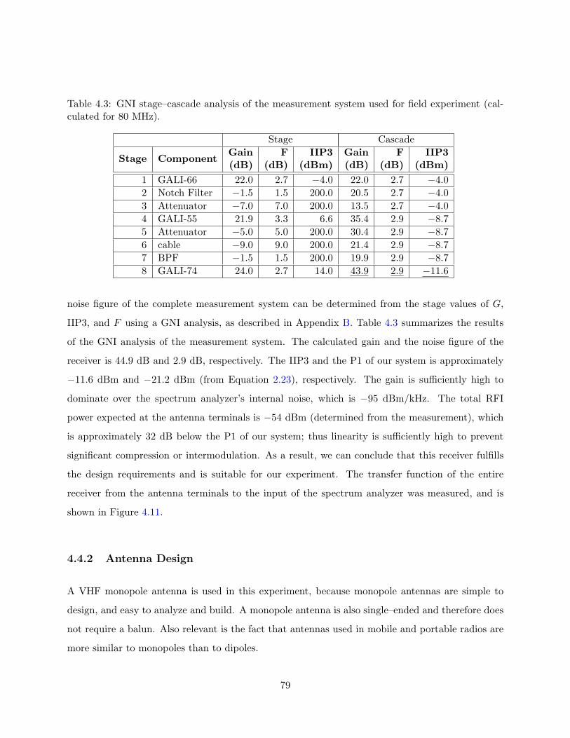
Table 4.3: GNI stage–cascade analysis of the measurement system used for field experiment (cal-culated for 80 MHz).
Stage Cascade
Stage ComponentGain F IIP3 Gain F IIP3(dB) (dB) (dBm) (dB) (dB) (dBm)
1 GALI-66 22.0 2.7 −4.0 22.0 2.7 −4.02 Notch Filter −1.5 1.5 200.0 20.5 2.7 −4.03 Attenuator −7.0 7.0 200.0 13.5 2.7 −4.04 GALI-55 21.9 3.3 6.6 35.4 2.9 −8.75 Attenuator −5.0 5.0 200.0 30.4 2.9 −8.76 cable −9.0 9.0 200.0 21.4 2.9 −8.77 BPF −1.5 1.5 200.0 19.9 2.9 −8.78 GALI-74 24.0 2.7 14.0 43.9 2.9 −11.6
noise figure of the complete measurement system can be determined from the stage values of G,
IIP3, and F using a GNI analysis, as described in Appendix B. Table 4.3 summarizes the results
of the GNI analysis of the measurement system. The calculated gain and the noise figure of the
receiver is 44.9 dB and 2.9 dB, respectively. The IIP3 and the P1 of our system is approximately
−11.6 dBm and −21.2 dBm (from Equation 2.23), respectively. The gain is sufficiently high to
dominate over the spectrum analyzer’s internal noise, which is −95 dBm/kHz. The total RFI
power expected at the antenna terminals is −54 dBm (determined from the measurement), which
is approximately 32 dB below the P1 of our system; thus linearity is sufficiently high to prevent
significant compression or intermodulation. As a result, we can conclude that this receiver fulfills
the design requirements and is suitable for our experiment. The transfer function of the entire
receiver from the antenna terminals to the input of the spectrum analyzer was measured, and is
shown in Figure 4.11.
4.4.2 Antenna Design
A VHF monopole antenna is used in this experiment, because monopole antennas are simple to
design, and easy to analyze and build. A monopole antenna is also single–ended and therefore does
not require a balun. Also relevant is the fact that antennas used in mobile and portable radios are
more similar to monopoles than to dipoles.
79

10 20 30 40 50 60 70 80 90-30
-20
-10
0
10
20
30
40
50
60
Frequency [MHz]
Gain
[d
B]
Figure 4.11: Transfer function of the receiver used in the field experiment.
80

The monopole antenna, shown in Figure 4.12, results from applying image theory to a half-wave
dipole. According to this theory, if a conducting plane is placed below a single element of length
L/2 carrying a current, then the combination of the element and its image acts identically to a
dipole of length L except that the radiation occurs only in the space above the plane. We used a
copper pipe 1.97 m long and 21 mm in diameter as our VHF monopole antenna.
Since the Earth is not a perfect ground, a ground screen is used above the Earth ground. Figure 4.13
shows the dimensions of the ground screen. It should be noted that the particular size and shape
of the ground screen was determined solely by the materials on hand, and is in no sense optimized.
Reflectix brand foil insulation8, which consists of two layers of aluminum foil with plastic bubble
laminated between the foil layers (mostly used for thermal insulation) is used as for the ground
screen for this experiment. The antenna is connected to the input of the receiver using a custom-
made “pig-tail” coaxial cable shown in Figure 4.14(a). To make the antenna stand upright during
the measurement, a wood dowel was inserted into the copper pipe and also driven into the ground,
as shown in Figure 4.14.
Commercial software FEKO9, which simulates an antenna using the Method of Moments (MoM),
is used to model this antenna as copper wire of circular cross section. In our simulation, the
ground screen is included above the the Earth ground, which is assumed to have conductivity
σ = 5 × 10⁻³ S/m and relative permittivity εr = 13. Figure 4.15 shows the resulting simulated
antenna impedance as well as the measured values. Simulated results indicate that this antenna is
resonant at around 36 MHz and the radiation resistance at the resonant frequency is 33.4Ω. The
measurement is in close agreement, indicating resonance at 34.6 MHz. However, it is noticeable
from Figure 4.15 that there are some discrepancies between the measured and simulated antenna
impedance. Since during the antenna impedance measurement we could not use any filter or other
components to block strong RFI that exists below 20 MHz (see Figure 4.18), we suspect that below
20 MHz this may cause measurement error. The reason behind the discrepancy above 40 MHz
is not known. However, the difference between the measured and simulated impedance in that
range has little effect on IME. This is illustrated in Figure 4.16, which shows the calculated IME
between the VHF monopole antenna and a preamplifier with Zp = 50Ω, using both the simulated
8Model#ST16025, http://www.reflectixinc.com9http://www.feko.info
81
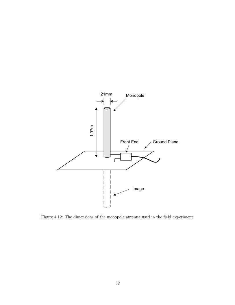
1.97m
21mm
Ground Plane
Monopole
Image
Front End
Figure 4.12: The dimensions of the monopole antenna used in the field experiment.
82

4.4 m
2.4 m
1.5 m
6.8 m
2.5 m
Antenna Location
Figure 4.13: The dimensions of the ground screen used in the field measurement as well as in thesimulation.
83
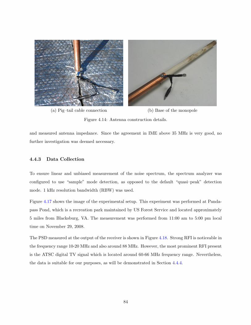
(a) Pig–tail cable connection (b) Base of the monopole
Figure 4.14: Antenna construction details.
and measured antenna impedance. Since the agreement in IME above 35 MHz is very good, no
further investigation was deemed necessary.
4.4.3 Data Collection
To ensure linear and unbiased measurement of the noise spectrum, the spectrum analyzer was
configured to use “sample” mode detection, as opposed to the default “quasi–peak” detection
mode. 1 kHz resolution bandwidth (RBW) was used.
Figure 4.17 shows the image of the experimental setup. This experiment was performed at Panda-
pass Pond, which is a recreation park maintained by US Forest Service and located approximately
5 miles from Blacksburg, VA. The measurement was performed from 11:00 am to 5:00 pm local
time on November 29, 2008.
The PSD measured at the output of the receiver is shown in Figure 4.18. Strong RFI is noticeable in
the frequency range 10-20 MHz and also around 88 MHz. However, the most prominent RFI present
is the ATSC digital TV signal which is located around 60-66 MHz frequency range. Nevertheless,
the data is suitable for our purposes, as will be demonstrated in Section 4.4.4.
84
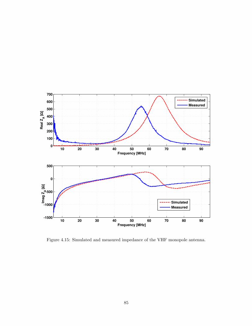
10 20 30 40 50 60 70 80 900
100
200
300
400
500
600
700
Real Z
A [
ΩΩ ΩΩ]
Frequency [MHz]
10 20 30 40 50 60 70 80 90-1500
-1000
-500
0
500
Frequency [MHz]
Imag
ZA [
ΩΩ ΩΩ]
Simulated
Measured
Simulated
Measured
Figure 4.15: Simulated and measured impedance of the VHF monopole antenna.
85
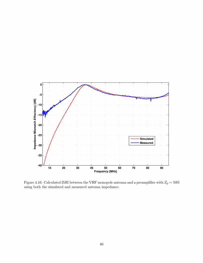
10 20 30 40 50 60 70 80 90-40
-35
-30
-25
-20
-15
-10
-5
0
Frequency [MHz]
Imp
ed
an
ce M
ism
atc
h E
ffie
cie
ncy [
dB
]
Simulated
Measured
Figure 4.16: Calculated IME between the VHF monopole antenna and a preamplifier with Zp = 50Ωusing both the simulated and measured antenna impedance.
86

Figure 4.17: Antenna and ground screen setup during the field experiment.
87

10 20 30 40 50 60 70 80 90-110
-100
-90
-80
-70
-60
-50
PS
D [
dB
m/R
BW
], R
BW
=1kH
z
Frequency [MHz]
Figure 4.18: Measured integrated PSD at the input of spectrum analyzer. Integrated over 500 mswith 1 kHz spectral resolution.
88

4.4.3.1 Problems Overcome
In the first attempts of this experiment using a preliminary version of the receiver, we observed
intermodulation due to the strong RFI signals apparent in Figure 4.18. This problem was solved
by (1) adding the BSF–108+ FM reject filter shown in Figure 4.8, and (2) introducing additional
attenuators between amplifier stages also as shown in Figure 4.8. Further investigation revealed
that low–level RFI from our measurement instruments was also appearing in the measured data.
The RFI was emitted from the data acquisition laptop PC, and also from an inverter which was
used to convert DC power into AC for the spectrum analyzer and laptop PC. To solve this problem,
the inverter was shut down during the measurement (the spectrum analyzer and the laptop PC
used their own internal batteries) and the laptop PC was relocated approximately 150 ft away from
the antenna using coaxial cable.
4.4.4 Results
Figure 4.19 shows the PSD of Galactic noise Sin referenced to the antenna terminals, i.e., at the
input of the receiver, including IME. Figure 4.19 also shows two predicted PSD curves; one com-
puted using the IME computed from the measured antenna impedance, and the second computed
using the IME from the simulated antenna impedance from Section 4.4.2. Modifying Equation 4.4,
the predicted value of Sin is calculated as
Sin = ηkTA
[1− |Γ|2
](4.10)
where TA is calculated as explained in the next paragraph.
The previously defined Galactic noise model provides the median value of the noise temperature.
However, in reality Galactic noise varies by approximately 3 dB as a function of time of day, and
this variation depends on the antenna pattern also. Therefore, in order to get a precise prediction
of PSD it is needed to use a more detailed and accurate model. This is done using a computer code
developed by K. Deshpande [81]. This code predicts antenna temperature due to Galactic noise
taking into account the location on the earth, antenna pattern, date, and time. It provides the
antenna temperature for the frequency of 38 MHz, however this temperature can be extrapolated
89

to other frequencies using the factor (ν/(38MHz))−2.55, where ν is the frequency in MHz [74]. In
summary, one of the main differences between the calculation of the Galactic noise temperature in
this way and using Table 4.2 is that this calculation includes the diurnal variation as well as the
antenna pattern and is thus more precise, whereas the calculation from Table 4.2 does not include
these.
The prediction curves in Figure 4.19 also incorporate ground loss, which is estimated using the
FEKO antenna simulation as follows: The antenna is simulated in transmission mode and the total
radiated power is measured. This is done twice: once for realistic lossy ground ( σ = 5 × 10⁻³
S/m, εr = 13), and once for perfectly conducting ground. The ratio of these radiated powers then
provides the ground loss efficiency. The finite ground screen was included during the simulation
for realistic lossy ground. On the other hand, for the perfectly conducting ground simulation, this
finite ground screen was excluded and the perfectly electric conducting ground plane was assumed
to be infinite. Figure 4.20 shows result. Note that the computed efficiency (η) varies between –5.3
dB and –3.4 dB.
Referring to Figure 4.19, note that the measured PSD closely follows the predicted PSD estimated
using the simulated antenna impedance. However, the measured PSD does not closely follow the
predicted PSD estimated using the measured antenna impedance, specifically at the lower frequency
region (below 35 MHz). The reason behind this probably the RFI–induced discrepancies between
the measured and simulation antenna impedance observed in Figure 4.15; thus the simulated result
is judged to be more accurate. Figure 4.21 shows the ratio of the predicted and the measured
PSD for the two different cases: in the first case predicted PSD is calculated using the simulated
antenna impedance, and in the second case predicted PSD is calculated using the measured an-
tenna impedance. Note the agreement is very good between 35 and 70 MHz, and the “dropout”
just above 60 MHz corresponds to the ATSC digital TV signal (Channel 3, 60–66 MHz). The
discrepancy between simulated and measured results below 35 MHz corresponds to the difference
in IME identified above. However, neither is particularly accurate in this region, perhaps because
the antenna reactance is very large (thus, important to know precisely) in this frequency range.
The error above 70 MHz probably due to the low γ; i.e., increasing contribution of internal noise
relative to external noise.
90

10 20 30 40 50 60 70 80 90-150
-140
-130
-120
-110
-100
-90
-80
Frequency [MHz]
PS
D [dB
m/R
BW
], R
BW
= 1
kH
z
Predicted result using measured ZA
Measured result
Predicted result using simulated ZA
ATSC Channel 3
FM Broadcast Band
Figure 4.19: PSD referenced to the antenna terminals.
91
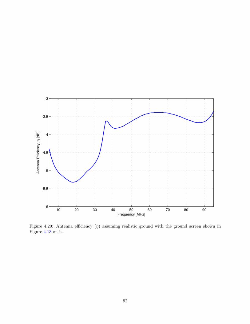
10 20 30 40 50 60 70 80 90-6
-5.5
-5
-4.5
-4
-3.5
-3
Frequency [MHz]
Ante
nna E
ffic
iency,
η [dB
]
Figure 4.20: Antenna efficiency (η) assuming realistic ground with the ground screen shown inFigure 4.13 on it.
92
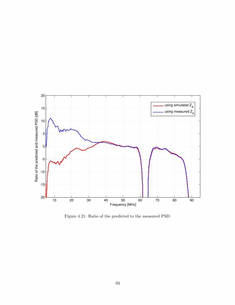
10 20 30 40 50 60 70 80 90-20
-15
-10
-5
0
5
10
15
20
Frequency [MHz]
Ratio o
f th
e p
redic
ted a
nd m
easure
d P
SD
[dB
]
using simulated ZA
using measured ZA
Figure 4.21: Ratio of the predicted to the measured PSD.
93

4.5 Summary
This chapter presented a concept to achieve “optimum” noise figure of a receiver from a sensitivity
point of view. If a front end is external noise–dominated then the matching requirement between
an antenna and a receiver can be loosened, and even a poor quality match can potentially provide
nearly the best possible sensitivity. The concept was validated through a field experiment mea-
suring Galactic noise using a VHF monopole antenna. Our measurement results closely follow the
predicted results over much of the frequency range 20–75 MHz and discrepancies can be attributed
to measurement or modeling errors. This experiment will be expanded in the next chapter to
measure the performance of a new kind of sensitivity–constrained multiplexer. The next chapter
describes the design methodology and performance analysis of this multiplexer.
94

Chapter 5
Multiplexer Design
Our goal is to present a design concept to build an RF front end for MMR to cover a large range
of frequency bands using just a single antenna. As is pointed out in Chapter 2, in order to fa-
cilitate this, it is needed to incorporate a multiplexer in our design. A multiplexer also plays
an important role to perform “preselection”, i.e., implementation of selectivity before frequency
conversion to manage intermodulation effects. Although antenna impedance varies significantly
with frequency, most of the traditional methodologies of multiplexer design assume constant in-
put/output impedance and do not consider external noise effects (described in Section 4.3). This
chapter presents a new multiplexer design methodology incorporating the concept described in
Chapter 4.
The organization of this chapter is as follows. Section 5.1 (“Classical Multiplexer Design Theory”)
discusses the classical theory of multiplexer design including its limitations. Current research trends
in multiplexer design are presented in Section 5.2 (“Research Trends in Multiplexer Design”). Sec-
tion 5.3 (“Sensitivity-Constrained Multiplexer Design”) describes the new sensitivity–constrained
multiplexer design concept. This design concept is demonstrated implementing an actual mul-
tiplexer for a VHF monopole antenna. The design description as well as detailed performance
analyses are presented in Section 5.4 (“VHF Monopole Multiplexer Design Example”). This chap-
ter is summarized in Section 5.5 (“Summary”).
95
5.1 Classical Multiplexer Design Theory
A multiplexer is a parallel or series combination of filters which is used to separate the input into
multiple frequency bands. Multiplexers are traditionally designed such that the impedance at all
ports is a standard value, such as 50 Ω. Common multiplexer types include diplexers (1:2 ports)
and triplexers (1:3 ports). An example of how a triplexer is used appears in Fig. 1.3. This section
briefly introduces classical multiplexer design theory and its limitations, which we want to overcome
in our design methodology.
It might at first appear that the design of the multiplexer could easily be accomplished by designing
the filters using any standard filter design procedures, and then connecting the filters in parallel
or series. However, in reality some interaction exists between the filters which could result in very
poor performance. This is demonstrated in Figures 5.1 and 5.2. Figure 5.1 shows the schematic of
two filters (a highpass and a lowpass) designed for 140 MHz cutoff frequency (at –1 dB) assuming
constant 50Ω termination impedance. Figure 5.2 compares the TPG performance when they are
connected individually and when they are connected together to 50Ω termination impedance. It
should be noted how the TPG performance get worse by simply connecting these filters together.
This interaction may be small for the filters with non–overlapping passbands, or filters with narrow
bandwidth (say, on the order of 1% bandwidth or less) and with guard bands between channels.
However for other cases, especially for filters with overlapping passbands, this interaction can be
significant. Therefore, an objective of multiplexer design is to employ techniques in order to avoid
those undesirable interactions between the filters.
Figures 5.3 and 5.4 show multiplexers for parallel–connected channels and for series–connected
channels, respectively. A useful reference on multiplexer design is Matthaei, Young and Jones [14],
which describes several methods to design multiplexers using these architectures. It presents design
methodology using narrow-band filters with guard bands between channels, as well as multiplexers
with contiguous passbands. These methods rely on the use of susceptance– or reactance–annulling
networks (as shown in Figure 5.3 and 5.4) to mitigate or reduce the imaginary part of the multi-
plexer’s total input admittance or reactance, respectively. Ideally, the combination of an annulling
network and the total input impedance of a multiplexer should provide a nearly constant total input
96

69.8 nH
33.4 pF
120.2 nH
33.4 pF
69.8 nH
50Ω
18.5 pF
38.7 nH
10.7 pF
38.7 nH
18.5 pF
+-gv
50Ω
50Ω
Figure 5.1: Circuit diagram of a diplexer. Each of the channels are designed for 50Ω terminationimpedance.
admittance or reactance, which approximates the generator conductance (Gg) or resistance (Rg),
across the operating band of the multiplexer. In Figure 5.3, Yi (i = 1, 2, . . . , n) represents the input
admittance (i.e. the reciprocal of impedance) of the corresponding multiplexer channels, which are
terminated by a constant conductance GL. B represents the value of susceptance in the annulling
network the purpose of which is to cancel the combined input admittance Yin between channel
filters. vg represents the voltage generated by the source (antenna in our case). In Figure 5.4, Zi
(i = 1, 2, . . . , n) represents the input impedance of the corresponding multiplexer channels, which
are terminated by a constant resistance RL. Zin is the total input impedance of the multiplexer
and X represents the value of reactance in the annulling network.
A strategy for classical design proceeds as follows. Consider the parallel form of Figure 5.4. In [44],
Bode shows that if the real part of an admittance (e.g., Yin in Figure 5.3) has the rectangular form
Re Yin = 0 , for 0 ≤ ω < ωa
= GL , for ωa ≤ ω < ωb
= 0 , for ωb ≤ ω < ∞ (5.1)
97
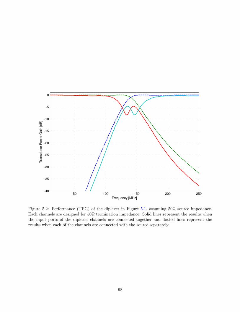
50 100 150 200 250-40
-35
-30
-25
-20
-15
-10
-5
0
Frequency [MHz]
Tra
nsducer
Pow
er
Gain
[dB
]
Figure 5.2: Performance (TPG) of the diplexer in Figure 5.1, assuming 50Ω source impedance.Each channels are designed for 50Ω termination impedance. Solid lines represent the results whenthe input ports of the diplexer channels are connected together and dotted lines represent theresults when each of the channels are connected with the source separately.
98
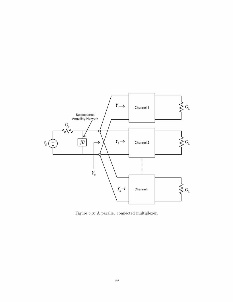
+-gv Channel 2
Channel 1
Channel n
gG
inY
jB
Susceptance
Annulling Network
1Y
2Y
nY
LG
LG
LG
Figure 5.3: A parallel–connected multiplexer.
99
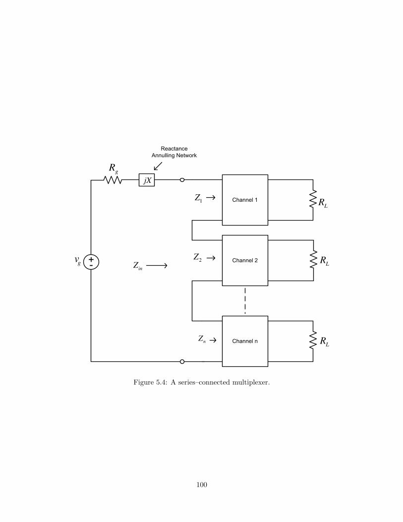
+-gv Channel 2
Channel 1
Channel n
gR
jX
Reactance
Annulling Network
1Z
LR
2Z
nZ
inZ LR
LR
Figure 5.4: A series–connected multiplexer.
100

then the imaginary part of the admittance can be expressed as
Im Yin =GL
πln
∣∣∣∣∣∣∣∣∣1 +
ω
ω0w −
(ω
ω0
)2
1− ω
ω0w −
(ω
ω0
)2
∣∣∣∣∣∣∣∣∣ (5.2)
where ω0 =√
ωaωb and w = (ωb − ωa)/ω0. Thus a suitable annulling reactance exists for at least
one frequency in ωa, ωb, and the bandwidth is limited by the tradeoff with TPG in the same
manner as described in Section 3.2.
Figure 5.5 shows the antenna matching application. Traditionally, the antenna impedance ZA(ω)
is assumed to be a real, constant value over the frequency range of interest. Let us call this RA0.
The resulting design equation becomes
RA0 = Zmux(ω) = Zmatch(ω) ‖ Zin(ω). (5.3)
The above equation needs to be solved for Zmatch(ω) to realize a matching circuit which transforms
the complex–valued input impedance of the multiplexer to a constant value, so that it can match
with RA0. The exact solution of this equation is very complex (perhaps not even possible) and
the complexity increases with the number of channels. Alternatively, an approximate solution can
potentially be found using a perturbation approach, i.e., starting with a crude initial solution,
linearizing the design equation in the region of that solution, and then iterating to get the desired
result. This approach permits the use of any design to implement the channelizing filters, but is not
guaranteed to yield a realizable or useful solution for the matching circuit. Typically, optimization
yields at best a loose fit to the requirement implied by Equation 5.3. The associated annulling
network is typically a parallel–resonator circuit.
The main problem with this state of affairs with respect to what is required for MMR receiver front
ends is that ZA(ω) cannot be assumed to be constant (even approximately) over large bandwidth,
as is demonstrated in Fig. 1.4. This issue has only recently begun to be addressed, as will be
discussed in the next section.
101

Channel 2
Channel 1
Channel n
( )in
Z ω
Matching Network
1( )Z ω
LR
2( )Z ω
( )nZ ω
( )match
Z ω
Antenna
( )muxZ ω
( )AZ ω
LR
LR
Figure 5.5: Multiplexer with parallel connected channels, input of which is connected with a match-ing circuit and an antenna.
102

5.2 Research Trends in Multiplexer Design
This section describes some recent research trends in multiplexer design.
Most of the current work on multiplexer design is for high frequency (GHz or more) applications.
Some examples are as follows. An example of a wideband 10–35 GHz six-channel microstrip mul-
tiplexer was described by Hong and Cheng (2006) in [82]. Each of the channels contain filters
centered at 10 GHz, 12 GHz, 19 GHz, 21 GHz, 32 GHz, and 35 GHz. All of these filters are
parallel–coupled microstrip bandpass filters composed of half–wavelength resonators with 500 MHz
bandwidth. Deng (2006) described a matching circuit for microstrip triplexer to minimize the inter-
action among the bandpass filters [83]. His methodology was demonstrated designing a multiplexer
with channels centered at 1.48 GHz, 1.75 GHz, and 1.98 GHz. Each of the channels provide ap-
proximately 5% fractional bandwidth. Another recent example of multiplexer design is a microstrip
four-channel multiplexer for a dual-band WLAN-UWB receiver, proposed by Lai and Jeng (2005)
in [84]. Each of the output ports consists of a dual–band bandpass filter: one with two passbands
from 2.1 to 2.9 GHz and from 5.1 to 5.9 GHz (for WLAN), and other with two passbands from 3.1
to 4.9 GHz and from 6.1 to 8.2 GHz (for UWB). In this work a Genetic algorithm (GA) technique
was employed to determine circuit topology and to overcome the interaction between the filters.
GA techniques might be useful in future development of a design methodology (the approach we
present in Section 5.3) to optimize the multiplexer channel filters.
An example of an innovative multiplexer design which uses passive circuit components in a frequency
range of greater interest was presented by Galbraith et. al. (2008) in [85]. A 20–channel multiplexer
with contiguous channels was demonstrated from the frequency range 20–90 MHz. The design of
this multiplexer is inspired by the cochlea of the human inner ear. The cochlea separates sound
into frequency bands with high selectivity using a very simple techniques; the analogous electrical
circuit is also relatively simple and effective. However, this approach is limited in the fractional
bandwidth of the channels, and thus is not entirely suitable for wideband mobile/portable MMR
applications.
A common feature of all of these above examples is the use of standard input/output impedances,
which is a constraint we wish to relax. However, researchers are only very recently beginning to
103
think about this. In [86], Wu and Meng (2007) present a direct synthesis approach for general
Chebyshev filters terminated by a complex load at one end and a real valued load on the other.
They presented a methodology to normalize the assumed complex matched impedance at one end
of the filter to the same real valued matched impedance as that at the other end of the filter so
that the existing synthesis techniques for general Chebyshev filters can be applied. The design
process starts with selecting the complex impedance (which needs to be matched) at the center
frequency of the filter. Then it is normalized to the reference impedance using the proposed design
methodology. Finally, they determine the necessary coefficients to realize the circuit. A diplexer,
the filters of which are centered at 1.74 GHz and 1.85 GHz frequency, is demonstrated using this
process. The bandwidth of both filters is approximately 80 MHz. Although this methodology helps
to design filters for complex termination impedance, it is still limited to achieve good matching
only at a single frequency per band instead of wide range of frequencies. This design methodology
is also limited to the use of filters with narrow fractional bandwidth.
In summary, no existing technique is entirely satisfactory for mobile/portable MMR, for the fol-
lowing reasons. Most of the previous techniques are for high frequency (GHz or more) and are
less useful to design multiplexers for low frequency (less than GHz), where discrete inductors and
capacitors must typically be used in lieu of wavelength–scale structures such as microstrip lines and
waveguides. The previous techniques are also limited by the use of either standard input/output
impedance or at best constant complex input/standard output impedance. Most of the described
techniques are also limited to narrow fractional bandwidth. We would like to relax these limita-
tions by using the concept described in Chapter 4 to design a new kind of sensitivity–constrained
multiplexer. The next section describes this concept in more detail.
5.3 Sensitivity-Constrained Multiplexer Design
This section explains the concept of sensitivity–constrained multiplexer design. To bypass some of
the difficulty associated with antenna matching, we propose an alternative design goal emphasizing
system sensitivity over impedance matching. This is motivated by the observation, made in Sec-
tion 4.2, that external noise can be very strong in practical scenarios, especially at low frequencies.
104

According to Equation 4.7, the ratio of external (unavoidable) noise to internally generated noise
is
γ(ω) = ηTA(ω)
Tp
[1− |Γ(ω)|2
](5.4)
where in this case reflection coefficient Γ(ω) is
Γ(ω) =Zmux(ω)− Z∗
A(ω)Zmux(ω) + Z∗
A(ω). (5.5)
Clearly, sensitivity is optimized by minimizing |Γ(ω)| (i.e., good matching) and minimizing Tp (i.e.,
low noise design). However, once γ is high (greater than about 5 or so), additional effort to minimize
|Γ(ω)| or Tp will have little effect on sensitivity. Furthermore, if acceptable γ can be achieved for
a poor |Γ(ω)| – as is possible when TA is large – improvements in |Γ(ω)| are actually counter-
productive, since this limits the design by imposing unnecessarily strict matching requirements.
Our proposed technique starts with designing each of the multiplexer channel filters for standard
(e.g., 50Ω) input and output impedance, connecting the input port of the multiplexer channels
together to the antenna, and then performing the optimization of the multiplexer channels according
to the following principles:
1. The ratio γ at the multiplexer output should be large, and
2. The multiplexer TPG should be “reasonably flat” over the passband.
Let the TPG of the channels be Ti(ω), where i = 1, 2, . . . , n represents the channel number; and the
value of components (i.e., inductors or capacitors) used in the channels is Xi,j , where j = 1, 2, . . . , p
represents the component numbers in each channel. The optimization is
minXi,j
n∑i=1
∫ ωb,i
ωa,i
[Ti(ω)− TBF,i]2 dω
(5.6)
where TBF,i is the theoretical TPG calculated using the Bode–Fano bound at the center frequency
of each channel; ωa,i and ωb,i are the lower and higher cutoff frequencies of each channel respectively.
This attempts to find Xi,j ’s such that the best possible fit to the optimum estimated per–channel
105

TPGs is obtained. Note that the quality of the fit is assessed using a mean–square error criteria.
Since it is likely that a perfect solution will not be found, we also specify a criteria for stopping the
optimization:
Ti(ω)|max − Ti(ω)|min < εi (5.7)
where Ti(ω)|max and Ti(ω)|min are the maximum and minimum values of the TPG over channel
i, and εi is a “flatness” constraint for each channel. Note that the starting point of selecting εi
can be the ripple of the Chebyshev filters which are originally designed for each channel. If the
optimization does not converge then depending on the need the value of εi can be increased.
Any multivariable optimization technique can be used to optimize the component values. The
optimization does not require or depend on any particular algorithm. This design methodology is
demonstrated in the next section.
5.4 VHF Monopole Multiplexer Design Example
In this section we demonstrate the method of sensitivity–constrained multiplexer design proposed
in Section 5.3, and evaluate the design in field conditions to confirm that the results are as ex-
pected. In this design example, we add a three–channel multiplexer to the VHF monopole antenna
described in Section 4.4.2, and use the same experimental system to conduct new measurements.
This section is organized as follows. Section 5.4.1 (“Problem Statement”) demonstrates the limi-
tation of classical (constant impedance) multiplexer design in the specific context of this example.
Section 5.4.2 (“Multiplexer Design”) presents an improved design using the sensitivity–constrained
approach. Section 5.4.3 (“Experiment Design”) and Section 5.4.4 (“Data Collection”) presents the
field experiment and data collection methodology, respectively. Finally, results are presented in
Section 5.4.5 (“Results”).
5.4.1 Problem Statement
Our goal is to interface the antenna shown in Figure 4.15 to separate receiver inputs corresponding
to the 10-28 MHz, 32-50 MHz, and 54-80 MHz bands. The interface concept of this multiplexer
106
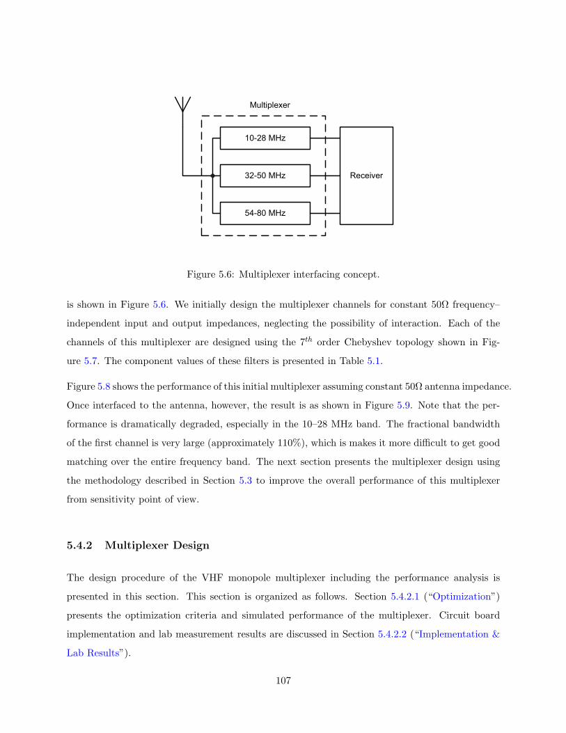
10-28 MHz
32-50 MHz
54-80 MHz
Receiver
Multiplexer
Figure 5.6: Multiplexer interfacing concept.
is shown in Figure 5.6. We initially design the multiplexer channels for constant 50Ω frequency–
independent input and output impedances, neglecting the possibility of interaction. Each of the
channels of this multiplexer are designed using the 7th order Chebyshev topology shown in Fig-
ure 5.7. The component values of these filters is presented in Table 5.1.
Figure 5.8 shows the performance of this initial multiplexer assuming constant 50Ω antenna impedance.
Once interfaced to the antenna, however, the result is as shown in Figure 5.9. Note that the per-
formance is dramatically degraded, especially in the 10–28 MHz band. The fractional bandwidth
of the first channel is very large (approximately 110%), which is makes it more difficult to get good
matching over the entire frequency band. The next section presents the multiplexer design using
the methodology described in Section 5.3 to improve the overall performance of this multiplexer
from sensitivity point of view.
5.4.2 Multiplexer Design
The design procedure of the VHF monopole multiplexer including the performance analysis is
presented in this section. This section is organized as follows. Section 5.4.2.1 (“Optimization”)
presents the optimization criteria and simulated performance of the multiplexer. Circuit board
implementation and lab measurement results are discussed in Section 5.4.2.2 (“Implementation &
Lab Results”).
107
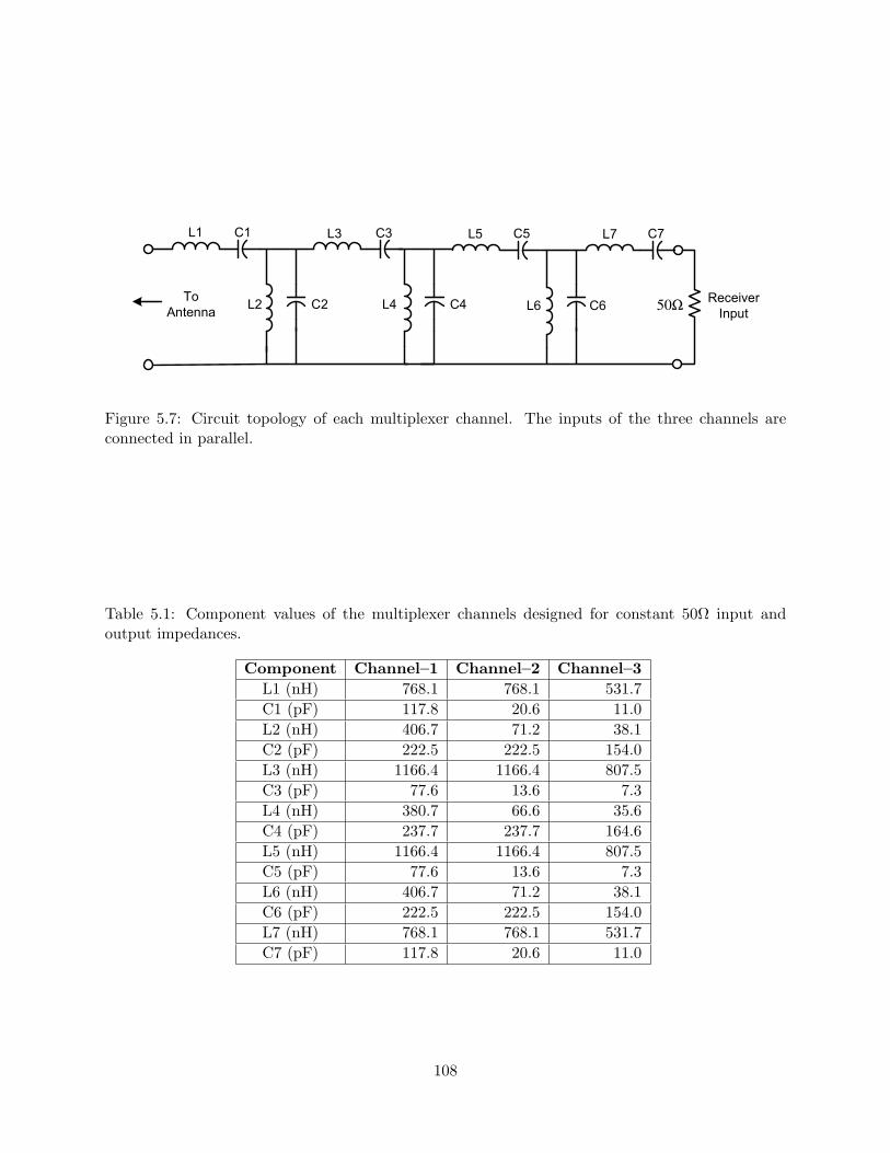
L1 C1
L2 C2
L3 C3
L4 C4
L5 C5
50ΩReceiver
InputTo Antenna
L1 C1
L2 C2
L3 C3
L4 C4
L5 C5
50ΩReceiver
Input
To
Antenna
L7 C7
L6 C6
Figure 5.7: Circuit topology of each multiplexer channel. The inputs of the three channels areconnected in parallel.
Table 5.1: Component values of the multiplexer channels designed for constant 50Ω input andoutput impedances.
Component Channel–1 Channel–2 Channel–3L1 (nH) 768.1 768.1 531.7C1 (pF) 117.8 20.6 11.0L2 (nH) 406.7 71.2 38.1C2 (pF) 222.5 222.5 154.0L3 (nH) 1166.4 1166.4 807.5C3 (pF) 77.6 13.6 7.3L4 (nH) 380.7 66.6 35.6C4 (pF) 237.7 237.7 164.6L5 (nH) 1166.4 1166.4 807.5C5 (pF) 77.6 13.6 7.3L6 (nH) 406.7 71.2 38.1C6 (pF) 222.5 222.5 154.0L7 (nH) 768.1 768.1 531.7C7 (pF) 117.8 20.6 11.0
108

10 20 30 40 50 60 70 80 90-50
-45
-40
-35
-30
-25
-20
-15
-10
-5
0
Frequency [MHz]
Tra
nsducer
Pow
er
Gain
[dB
]
Figure 5.8: Performance (TPG) of the initial (50Ω–in, 50Ω–out) multiplexer, assuming constant 50Ωsource impedance. Solid lines represent the results when input port of all multiplexer channels areconnected together and dotted lines represent the results when each of the channels are connectedwith the source separately.
109
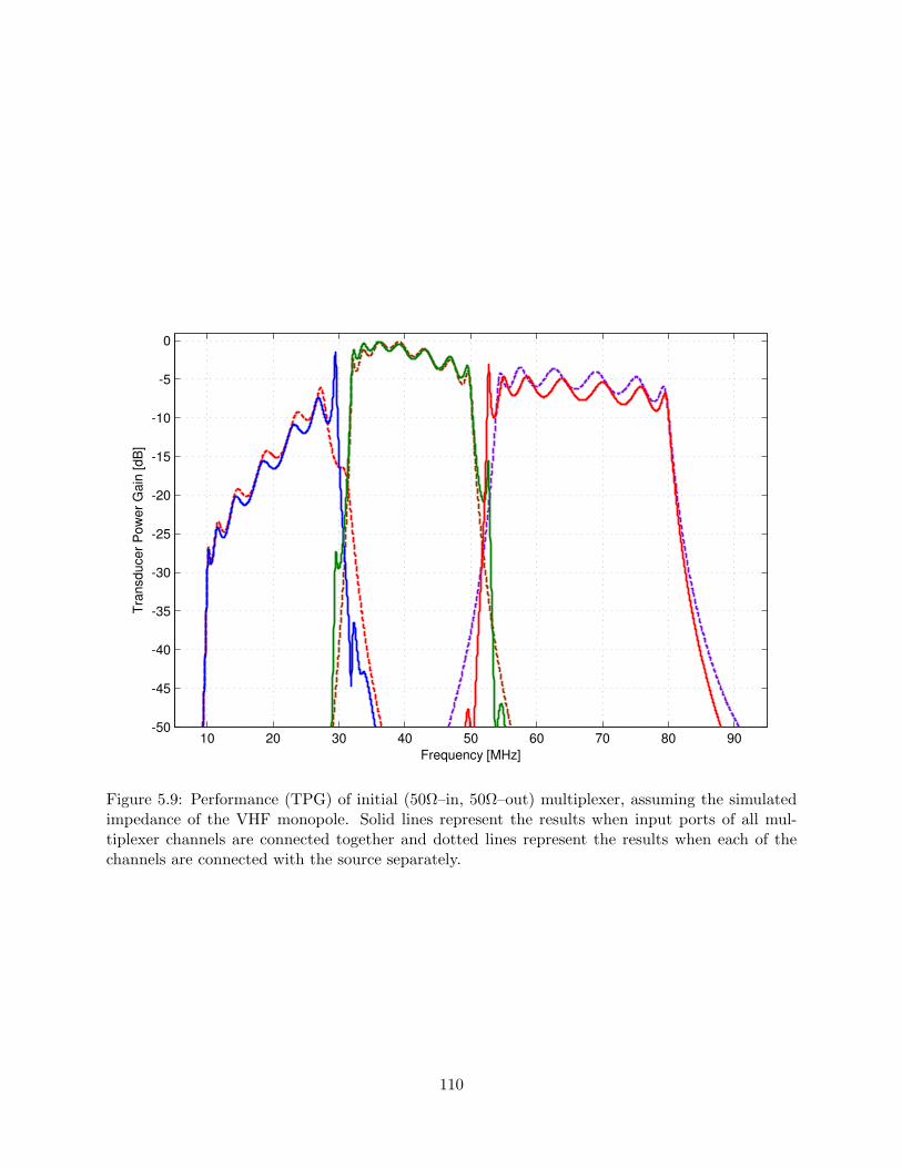
10 20 30 40 50 60 70 80 90-50
-45
-40
-35
-30
-25
-20
-15
-10
-5
0
Frequency [MHz]
Tra
nsducer
Pow
er
Gain
[dB
]
Figure 5.9: Performance (TPG) of initial (50Ω–in, 50Ω–out) multiplexer, assuming the simulatedimpedance of the VHF monopole. Solid lines represent the results when input ports of all mul-tiplexer channels are connected together and dotted lines represent the results when each of thechannels are connected with the source separately.
110

Table 5.2: Maximum theoretical TPG calculated from Bode–Fano limits assuming best fit RC/RLantenna impedances. n is the order of Chebyshev matching filter.
Parameter Channel–1 Channel–2 Channel–3(10–28 MHz) (32–50 MHz) (54–80 MHz)
f0 16.73 MHz 40 MHz 65.73 MHzB 110% 40% 50%ZA(f0) 4.9− j296.5 Ω 52.5 + j48.0 Ω 674.4− j41.6 ΩR 4.9 Ω 52.5 Ω 674.4 ΩSeries C or L 32.0 pF 191.0 nH 58.2 pF|Γ(f0)|min 0.95 4.8× 10⁻⁴ 1.2× 10−56
TPG (n = ∞) −10.4 dB ≈ 0 dB ≈ 0 dBTPG (n = 7) −13.8 dB ≈ 0 dB ≈ 0 dB
5.4.2.1 Optimization
Before starting the optimization we need to have an idea about the theoretically best possible
TPG, i.e., the maximum possible TPG for both infinite number of matching sections as well as 7th
order Chebyshev topology in a matching circuit, from the Bode–Fano bound using the equations
in Section 3.2.1 for each multiplexer channel. To calculate the Bode–Fano bound, the antenna
impedance is approximated using a series RC or series RL model in our desired frequency band.
The procedure is specifically as follows:
1. For each channels’ geometric center frequency (f0), the impedance of the VHF monopole
antenna is calculated.
2. From this impedance we calculate the value of the series resistance R, and the series ca-
pacitance C or series inductance L (depending on the positive or negative reactance value).
Figure 5.10 shows the antenna impedance calculated from the series RC and series RL ap-
proximation of the VHF monopole antenna, compared to the actual (simulated) values.
3. Using these values and the fractional bandwidths of each channel, the theoretical TPG is
calculated using Equations 3.13 to 3.18. The results are shown in Table 5.2. This table also
shows the TPG limit for a matching circuit using 7th order Chebyshev topology.
111
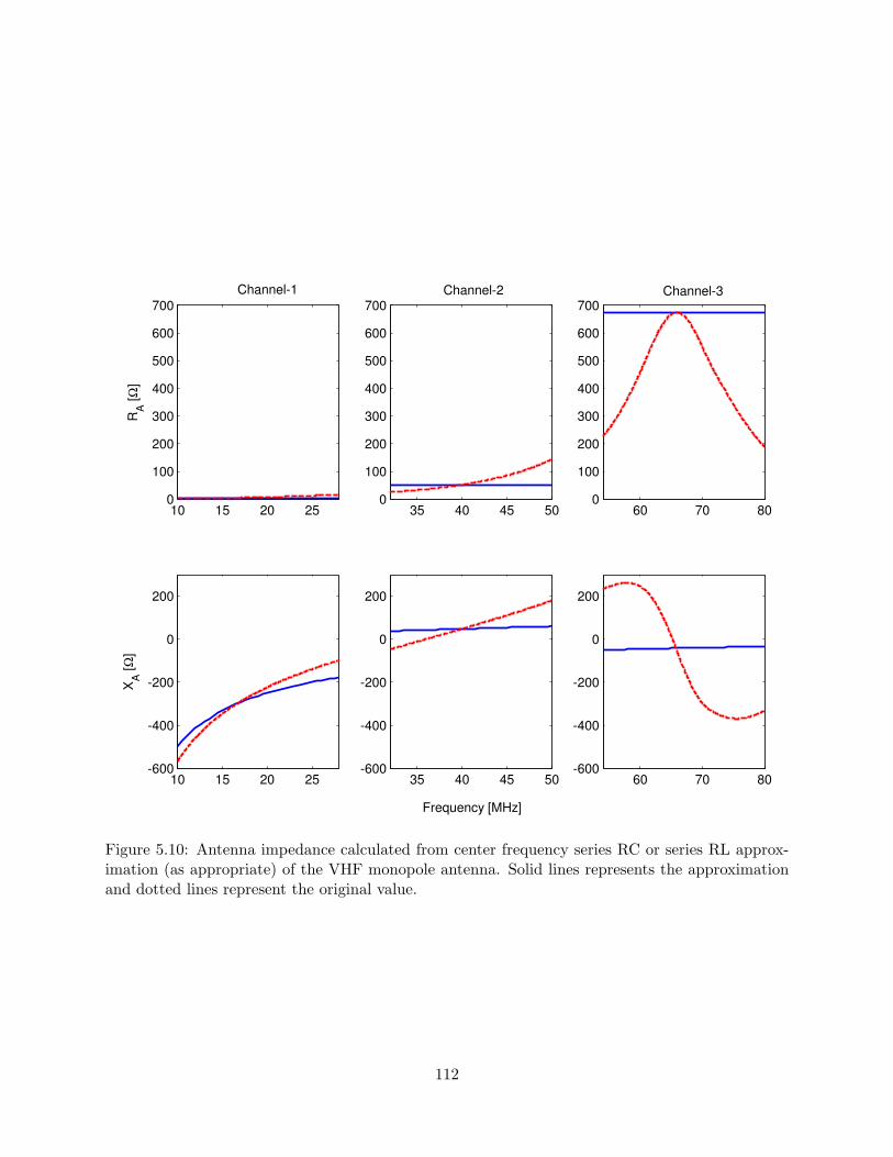
10 15 20 250
100
200
300
400
500
600
700
RA [
Ω]
35 40 45 500
100
200
300
400
500
600
700
60 70 800
100
200
300
400
500
600
700
10 15 20 25-600
-400
-200
0
200
XA [
Ω]
35 40 45 50-600
-400
-200
0
200
60 70 80-600
-400
-200
0
200
Frequency [MHz]
Channel-1 Channel-2 Channel-3
Figure 5.10: Antenna impedance calculated from center frequency series RC or series RL approx-imation (as appropriate) of the VHF monopole antenna. Solid lines represents the approximationand dotted lines represent the original value.
112
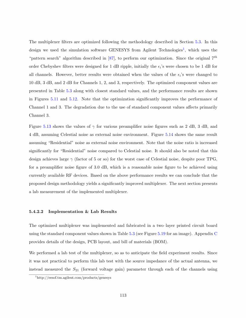
The multiplexer filters are optimized following the methodology described in Section 5.3. In this
design we used the simulation software GENESYS from Agilent Technologies1, which uses the
“pattern search” algorithm described in [87], to perform our optimization. Since the original 7th
order Chebyshev filters were designed for 1 dB ripple, initially the εi’s were chosen to be 1 dB for
all channels. However, better results were obtained when the values of the εi’s were changed to
10 dB, 3 dB, and 2 dB for Channels 1, 2, and 3, respectively. The optimized component values are
presented in Table 5.3 along with closest standard values, and the performance results are shown
in Figures 5.11 and 5.12. Note that the optimization significantly improves the performance of
Channel 1 and 3. The degradation due to the use of standard component values affects primarily
Channel 3.
Figure 5.13 shows the values of γ for various preamplifier noise figures such as 2 dB, 3 dB, and
4 dB, assuming Celestial noise as external noise environment. Figure 5.14 shows the same result
assuming “Residential” noise as external noise environment. Note that the noise ratio is increased
significantly for “Residential” noise compared to Celestial noise. It should also be noted that this
design achieves large γ (factor of 5 or so) for the worst case of Celestial noise, despite poor TPG,
for a preamplifier noise figure of 3.0 dB, which is a reasonable noise figure to be achieved using
currently available RF devices. Based on the above performance results we can conclude that the
proposed design methodology yields a significantly improved multiplexer. The next section presents
a lab measurement of the implemented multiplexer.
5.4.2.2 Implementation & Lab Results
The optimized multiplexer was implemented and fabricated in a two–layer printed circuit board
using the standard component values shown in Table 5.3 (see Figure 5.19 for an image). Appendix C
provides details of the design, PCB layout, and bill of materials (BOM).
We performed a lab test of the multiplexer, so as to anticipate the field experiment results. Since
it was not practical to perform this lab test with the source impedance of the actual antenna, we
instead measured the S21 (forward voltage gain) parameter through each of the channels using1http://eesof.tm.agilent.com/products/genesys
113

10 20 30 40 50 60 70 80 90-50
-45
-40
-35
-30
-25
-20
-15
-10
-5
0
Frequency [MHz]
Tra
nsducer
Pow
er
Gain
[dB
]
Figure 5.11: Performance (TPG) of optimized multiplexer, assuming simulated impedance of VHFmonopole. Solid lines represent the results after optimization and dotted lines represent the resultsbefore optimization.
114

10 20 30 40 50 60 70 80 90-50
-45
-40
-35
-30
-25
-20
-15
-10
-5
0
Frequency [MHz]
Tra
nsducer
Pow
er
Gain
[dB
]
Figure 5.12: Performance (TPG) comparison of optimized multiplexer for original and standardcomponent values. Solid lines represent the performance using standard component values anddotted lines represent the performance using original values.
115

10 20 30 40 50 60 70 80 900
5
10
15
20
25
30
35
Frequency [MHz]
Ratio o
f E
xte
rnal to
Inte
rnal N
ois
e [Lin
ear
Units]
F = 2 dB
F = 3 dB
F = 4 dB
Figure 5.13: Performance (γ) of optimized multiplexer (using standard component values) for 2, 3,and 4 dB preamplifier noise figures, assuming simulated impedance of the VHF monopole antennaand Celestial noise.
116

10 20 30 40 50 60 70 80 900
200
400
600
800
1000
1200
Frequency [MHz]
Ratio o
f E
xte
rnal to
Inte
rnal N
ois
e [Lin
ear
Units]
F = 2 dB
F = 3 dB
NF = 4 dB
Figure 5.14: Performance (γ) of optimized multiplexer (using standard component values) for 2, 3,and 4 dB preamplifier noise figures, assuming simulated impedance of the VHF monopole antennaand “Residential” noise.
117
Table 5.3: Original and nearest standard component values for the multiplexer after the optimiza-tion for the simulated impedance of the VHF monopole antenna.
Component Channel–1 Channel–2 Channel–3Original Standard Original Standard Original Standard
L1 (nH) 1201.9 1198.0 1179.7 1198.0 1.3 22.0C1 (pF) 10000.0 10000.0 15.8 15.0 17.1 18.0L2 (nH) 545.9 538.0 102.2 100.0 41.5 47.0C2 (pF) 183.9 180.0 152.8 150.0 133.9 120.0L3 (nH) 1500.0 1498.0 1441.8 1456.0 906.2 960.0C3 (pF) 54.6 56.0 10.8 10.0 6.3 6.2L4 (nH) 433.9 538.0 78.2 82.0 35.1 39.0C4 (pF) 214.8 180.0 204.9 180.0 165.8 150.0L5 (nH) 1332.9 1336.0 1194.4 1198.0 795.9 784.0C5 (pF) 64.0 68.0 13.3 12.0 7.3 7.5L6 (nH) 368.4 380.0 69.7 68.0 34.2 33.0C6 (pF) 235.9 220.0 231.5 220.0 170.2 180.0L7 (nH) 753.2 737.0 594.6 538.0 383.8 380.0C7 (pF) 109.5 120.0 27.3 27.0 15.2 15.0
50Ω source and load impedance. We then compared this to the S21 calculated using simulation.
The TPG for the 50Ω input condition is calculated in GENESYS using both the measured and
simulated S21. Figure 5.15 shows the results. Although Channel 1 agrees with the simulation
result closely, the other two channels are little bit off from the simulation result. The reason
behind this is believed to be due to parasitic reactances in the PCB layout. A similar problem
is described in [85], in which the authors intended to implement a multiplexer in approximately
the same frequency region (20–90 MHz) using similar (air–core) inductors. They claimed to have
solved the problem with the assistance of simulations accounting for board parasitics using the full–
wave electromagnetic simulator “Sonet EM” from Sonet Software, Inc2. They also used trimmer
capacitors to facilitate fine adjustments. We did not try to implement these solutions due to the
schedule and funding limitations of our project.
The TPG for the field measurement can be predicted using the measured S21 of the multiplexer.
The simulated S21 is replaced with the measured S21, and the predicted TPG is then calculated
using the actual antenna impedance as the source impedance. Figure 5.16 shows the predicted TPG
for the field experiment. Figure 5.17 shows the values of γ for various preamplifier noise figures2http://www.sonnetsoftware.com/
118
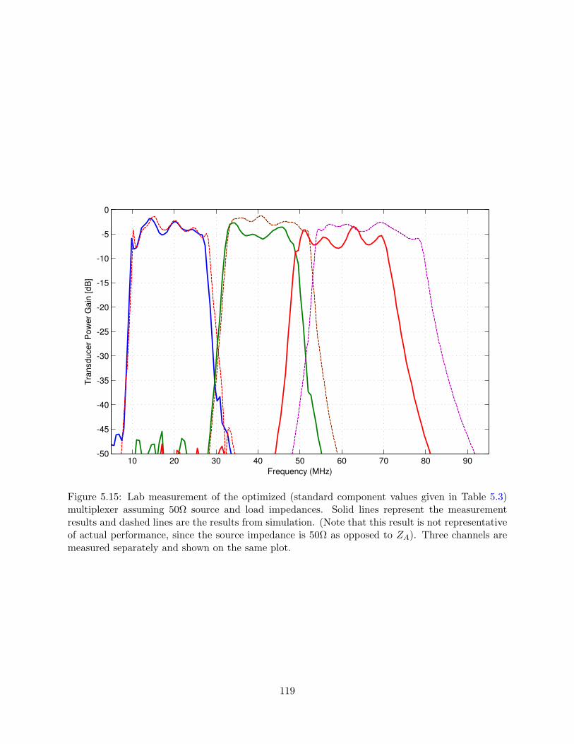
10 20 30 40 50 60 70 80 90-50
-45
-40
-35
-30
-25
-20
-15
-10
-5
0
Frequency (MHz)
Tra
nsducer
Pow
er
Gain
[dB
]
Figure 5.15: Lab measurement of the optimized (standard component values given in Table 5.3)multiplexer assuming 50Ω source and load impedances. Solid lines represent the measurementresults and dashed lines are the results from simulation. (Note that this result is not representativeof actual performance, since the source impedance is 50Ω as opposed to ZA). Three channels aremeasured separately and shown on the same plot.
119
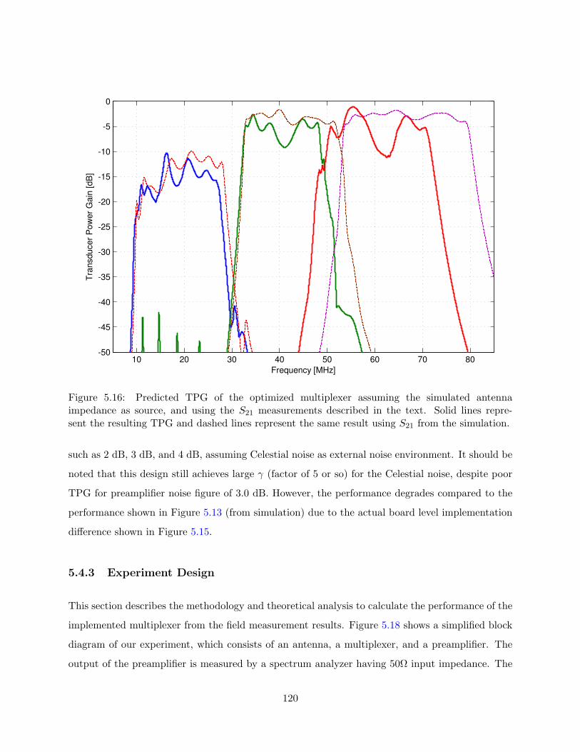
10 20 30 40 50 60 70 80-50
-45
-40
-35
-30
-25
-20
-15
-10
-5
0
Frequency [MHz]
Tra
nsducer
Pow
er
Gain
[dB
]
Figure 5.16: Predicted TPG of the optimized multiplexer assuming the simulated antennaimpedance as source, and using the S21 measurements described in the text. Solid lines repre-sent the resulting TPG and dashed lines represent the same result using S21 from the simulation.
such as 2 dB, 3 dB, and 4 dB, assuming Celestial noise as external noise environment. It should be
noted that this design still achieves large γ (factor of 5 or so) for the Celestial noise, despite poor
TPG for preamplifier noise figure of 3.0 dB. However, the performance degrades compared to the
performance shown in Figure 5.13 (from simulation) due to the actual board level implementation
difference shown in Figure 5.15.
5.4.3 Experiment Design
This section describes the methodology and theoretical analysis to calculate the performance of the
implemented multiplexer from the field measurement results. Figure 5.18 shows a simplified block
diagram of our experiment, which consists of an antenna, a multiplexer, and a preamplifier. The
output of the preamplifier is measured by a spectrum analyzer having 50Ω input impedance. The
120

10 20 30 40 50 60 70 80 900
5
10
15
20
25
30
35
40
Frequency [MHz]
Ratio o
f E
xte
rnal to
Inte
rnal N
ois
e [Lin
ear
Units]
F = 2 dB
F = 3 dB
F = 4 dB
Figure 5.17: Performance (γ) of optimized implemented multiplexer (using standard components)for 2, 3, and 4 dB preamplifier noise figures, assuming simulated impedance of the VHF monopoleantenna and Celestial noise as external noise environment, based on the S21 measurements describedin the text.
121

antenna is the same antenna described in Chapter 4, and the preamplifier represents the receiver
described in Chapter 4.
The PSD at the antenna terminals is
SA = ηkTA (5.8)
When no multiplexer is used, we have
S(1)out = SA
(1−
∣∣∣Γ(1)A
∣∣∣2) GP + kTP GP (5.9)
where Γ(1)A in this case (no multiplexer in Figure 5.18) is ΓP , i.e., the reflection coefficient at the
interface of antenna and the preamplifier, TP is the noise temperature of the preamplifier, and GP
is the total gain of the preamplifier. An estimate of SA, the PSD that the antenna delivers to a
perfectly matched load, is therefore given by
SA =S
(1)out − kTP GP(
1−∣∣∣Γ(1)
A
∣∣∣2) GP
(5.10)
Channel
Filter+-
50
Antenna Preamplifier
AZ
~
,A nV Ω
Multiplexer
AΓ PΓ
AS P
SoutS
FG
pG
pT,
Figure 5.18: Analysis of the experiment used to determine multiplexer channel TPG.
122
When the multiplexer is included, we have
S(2)out = S
(2)P GP + kTP GP (5.11)
Now the PSD S(2)P delivered to the preamplifier by the multiplexer channel under test can be
estimated as
S(2)P =
S(2)out − kTP GP
GP(5.12)
Combining Equations 5.10 and 5.12, the TPG of the multiplexer can be calculated from measure-
ments of S(1)out and S
(2)out as
TPG =S
(2)P
SA
=S
(2)out − kTP GP
S(1)out − kTP GP
(1−
∣∣∣Γ(1)A
∣∣∣2) (5.13)
5.4.4 Data Collection
Figure 5.19 shows the multiplexer as used during the field measurement. Figure 5.20 shows the
integrated S(2)out for all three channels, and S
(1)out.
5.4.5 Results
From the measurements of S(1)out and S
(2)out the TPG for each multiplexer channel is calculated using
Equation 5.13, where the value of Tp is obtained from the preamplifier noise figure (F = 2.9 dB)
calculated in Table 4.3, and Gp can be found from Figure 4.11. Figure 5.21 shows the resulting
measured TPG as well as the predicted TPG. Note that some strong RFI is present (especially
at lower frequencies) in our measurement data . In our calculation process, we performed window
averaging to make the measurement data smooth, thereby reducing the effect of RFI. However, we
can get the idea from the Figure 5.21 that the measured performance closely follows the predicted
performance.
Note that the measured responses do not roll off sharply at the band edges as the predicted responses
do. This is because after the cutoff frequencies of multiplexer filters the receiver becomes dominated
by its internal noise instead of external noise.
123

Figure 5.19: The multiplexer in the process of field testing.
Figure 5.22 shows the ratio of the measured and the predicted TPG of the multiplexer. The
measured TPG is within approximately ±5 dB for Channel 1, ±3 dB for Channel 2, and ±4 dB for
Channel 3, with respect to the predicted TPG. The large and rapidly frequency–varying difference
between the predicted and measured TPG for Channel 1 is primarily due to RFI, which has been
reduced but not completely eliminated by the averaging described above. Channels 2 and 3 are
less affected by this problem, as expected. The mean ratio over each channel is very close to the
expected value of unity, with the error being attributable to a combination of differences in the
ripple structure in the frequency responses, and incompletely suppressed RFI. This seems to be
confirmed by the fact that Channel 2, which contains less RFI compared to the other channels,
provides TPG performance close to the predicted TPG compared to the other channels.
124

10 20 30 40 50 60 70 80 90-180
-170
-160
-150
10 20 30 40 50 60 70 80 90-180
-170
-160
-150
10 20 30 40 50 60 70 80 90-180
-170
-160
-150
10 20 30 40 50 60 70 80 90-180
-170
-160
-150
Frequency [MHz]
PS
D [dB
m/R
BW
], R
BW
= 1
kH
z
S(2)
out for Ch-1
S(2)
out for Ch-2
S(2)
out for Ch-3
S(1)
out
Figure 5.20: Measured integrated PSD for each multiplexer channel, and also without the multi-plexer. Integrated over 500 ms with 1 kHz spectral resolution.
125

10 20 30-50
-45
-40
-35
-30
-25
-20
-15
-10
-5
0
Frequency [MHz]
Tra
nsducer
Pow
er
Gain
[dB
]
Channel-1
30 35 40 45 50 55-50
-45
-40
-35
-30
-25
-20
-15
-10
-5
Frequency [MHz]
Channel-2
50 60 70 80-50
-45
-40
-35
-30
-25
-20
-15
-10
-5
0
Frequency [MHz]
Channel-3
Figure 5.21: Performance (TPG) of the multiplexer as built with standard component values. Solidlines represent the measured TPG from the field experiment and dotted lines represent the predictedTPG based on the S21 measurements shown in Figure 5.16.
126

10 12 14 16 18 20 22 24 26 28-10
-5
0
5
10
32 34 36 38 40 42 44 46 48 50-10
-5
0
5
10
Ratio o
f th
e P
redic
ted a
nd M
easure
d T
PG
[dB
]
52 54 56 58 60 62 64 66 68 70-10
-5
0
5
10
Frequency [MHz]
Channel 1
Channel 2
Channel 3
Figure 5.22: Ratio of the predicted to the measured TPG.
127
5.5 Summary
This chapter presented a multiplexer design methodology emphasizing sensitivity, rather than
match efficiency, exploiting the dominance of environmental noise over a receiver’s internal noise.
We demonstrated the technique by designing and implementing a multiplexer to interface with a
VHF monopole antenna for operation in three frequency bands – 10–28 MHz, 32–50 MHz, and 54-80
MHz. It has been shown from the field experiment that the performance (TPG) of the multiplexer
follows the predicted performance. Despite poor TPG, the designed multiplexer achieves large γ
(factor of 5 or so) in an environment consisting primarily of Celestial (as opposed to man–made)
noise environment for a preamplifier noise figure of 3 dB. The ratio γ in environments including
significant man–made noise would be much greater. The performance of this multiplexer can be
further improved incorporating the parasitic effects (from the PC board) in the design during the
board level implementation. Next chapter describes the design of a multiplexer to integrate a MMR
receiver with a single antenna to operate at frequencies above 100 MHz.
128

Chapter 6
Multiplexer Application to a
Multiband Multimode Radio
A multiband multimode radio has been designed and developed at Virginia Tech for public safety
applications. In this radio, the Motorola RFIC described in Section 7.3 is interfaced with a single
monopole antenna using a four channel multiplexer, based on the design concepts of Chapter 5. This
chapter presents the design and performance analysis of this multiplexer (the rest of the radio is
described in Chapter 7). Initially, this multiplexer is designed for a simple 20 cm monopole antenna
of 5 mm radius, to provide a generic example of performance [88]. Section 6.1 (“Multiplexer Design
for a Generic Monopole Antenna”) presents the design and performance analysis of this multiplexer.
Then a multiplexer is designed for a commercially–available monopole antenna 18 cm long and 6
mm diameter. The design and performance analysis of this multiplexer is discussed in Section 6.2
(“Multiplexer Design for a Real Antenna”). Section 6.3 (“Summary”) summarizes this chapter.
6.1 Multiplexer Design for a Generic Monopole Antenna
We wish to interface a monopole antenna to separate receiver inputs using the multiplexer architec-
ture and frequency bands shown in Figure 6.1 incorporating the same design procedure described
in Chapter 5. Initially, the multiplexer channels are designed for a constant 50Ω termination
129

impedance using the 5th order Chebyshev topology shown in Figure 6.2.
The starting component values for this design are presented in Table 6.1. The performance of this
multiplexer, assuming constant 50Ω antenna impedance, is shown in Figure 6.3. It should be noted
that the interaction between the channels is negligible when antenna impedance is assumed to be
50Ω since the multiplexer is designed for constant 50Ω termination impedance and the presence of
wide separation between channels.
6.1.1 Optimization
The VT MMR is designed to achieve performance comparable to existing radios, using the same
monopole–type antennas already in use. Hence the multiplexer for this radio is designed to accom-
modate a generic “rod” monopole antenna 20 cm long and 5 mm in radius, the dimensions of which
are comparable to antennas used by existing radios. Another reason for considering this antenna
first is because we want to explore the performance of our proposed technique using a simple and
easy–to–model antenna first, and we will design it for an actual antenna later.
The monopole is modeled in the manner shown in Figure 2.3, as a voltage source in series with an
antenna impedance ZA which is equal to one–half the impedance of corresponding dipole (obtained
using image theory) in free space. We obtain a circuit model for ZA using the TTG method de-
scribed in Section 2.2. The circuit model and associated impedance are shown in Figure 6.4 and 6.5,
respectively. Figure 6.5 also shows the impedance calculated using the method of moments (MoM)
for comparison purpose only. Note that both methods of analysis are in reasonable agreement
between 100 and 450 MHz. The TTG method resulted in a circuit model that is resonant at 341
MHz, slightly lower than the anticipated resonance of 347 MHz, which was correctly predicted by
the MoM. The TTG method produces a radiation resistance of approximately 30Ω at resonance,
whereas MoM produces 36Ω at resonance. From this comparison we can conclude that the circuit
model attained from the TTG method is a reasonable characterization of the impedance of a dipole
or monopole antenna over at least half of our desired range of frequencies (138–862 MHz). In fact
the TTG model is suitable for our purposes over the entire range of interest. This is demonstrated
by the calculated IME shown in Figure 6.6.
130
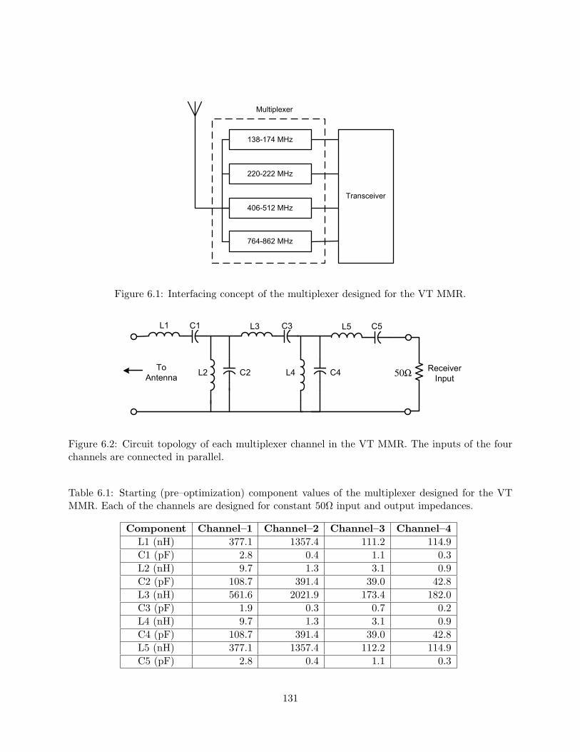
138-174 MHz
220-222 MHz
406-512 MHz
Transceiver
Multiplexer
764-862 MHz
Figure 6.1: Interfacing concept of the multiplexer designed for the VT MMR.
L1 C1
L2 C2
L3 C3
L4 C4
L5 C5
50ΩReceiver
InputTo Antenna
L1 C1
L2 C2
L3 C3
L4 C4
L5 C5
50ΩReceiver
Input
To
Antenna
L7 C7
L6 C6
L1 C1
L2 C2
L3 C3
L4 C4
L5 C5
50ΩReceiver
Input
To
Antenna
Figure 6.2: Circuit topology of each multiplexer channel in the VT MMR. The inputs of the fourchannels are connected in parallel.
Table 6.1: Starting (pre–optimization) component values of the multiplexer designed for the VTMMR. Each of the channels are designed for constant 50Ω input and output impedances.
Component Channel–1 Channel–2 Channel–3 Channel–4L1 (nH) 377.1 1357.4 111.2 114.9C1 (pF) 2.8 0.4 1.1 0.3L2 (nH) 9.7 1.3 3.1 0.9C2 (pF) 108.7 391.4 39.0 42.8L3 (nH) 561.6 2021.9 173.4 182.0C3 (pF) 1.9 0.3 0.7 0.2L4 (nH) 9.7 1.3 3.1 0.9C4 (pF) 108.7 391.4 39.0 42.8L5 (nH) 377.1 1357.4 112.2 114.9C5 (pF) 2.8 0.4 1.1 0.3
131

100 200 300 400 500 600 700 800 900-50
-45
-40
-35
-30
-25
-20
-15
-10
-5
0
Frequency [MHz]
Tra
nsducer
Pow
er
Gain
[dB
]
Figure 6.3: Performance (TPG) of initial (50Ω–in, 50Ω–out) multiplexer designed for the VT MMR,assuming constant 50Ω antenna impedance.
132
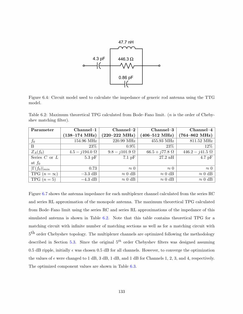
Ω4.3 pF
47.7 nH
446.3
0.86 pF
Figure 6.4: Circuit model used to calculate the impedance of generic rod antenna using the TTGmodel.
Table 6.2: Maximum theoretical TPG calculated from Bode–Fano limit. (n is the order of Cheby-shev matching filter).
Parameter Channel–1 Channel–2 Channel–3 Channel–4(138–174 MHz) (220–222 MHz) (406–512 MHz) (764–862 MHz)
f0 154.96 MHz 220.99 MHz 455.93 MHz 811.52 MHzB 23% 0.9% 23% 12%ZA(f0) 4.5− j194.0 Ω 9.8− j101.9 Ω 66.5 + j77.8 Ω 446.2− j41.5 ΩSeries C or Lat f0
5.3 pF 7.1 pF 27.2 nH 4.7 pF
|Γ(f0)|min 0.73 ≈ 0 ≈ 0 ≈ 0TPG (n = ∞) −3.3 dB ≈ 0 dB ≈ 0 dB ≈ 0 dBTPG (n = 5) −4.3 dB ≈ 0 dB ≈ 0 dB ≈ 0 dB
Figure 6.7 shows the antenna impedance for each multiplexer channel calculated from the series RC
and series RL approximation of the monopole antenna. The maximum theoretical TPG calculated
from Bode–Fano limit using the series RC and series RL approximations of the impedance of this
simulated antenna is shown in Table 6.2. Note that this table contains theoretical TPG for a
matching circuit with infinite number of matching sections as well as for a matching circuit with
5th order Chebyshev topology. The multiplexer channels are optimized following the methodology
described in Section 5.3. Since the original 5th order Chebyshev filters was designed assuming
0.5 dB ripple, initially ε was chosen 0.5 dB for all channels. However, to converge the optimization
the values of ε were changed to 1 dB, 3 dB, 1 dB, and 1 dB for Channels 1, 2, 3, and 4, respectively.
The optimized component values are shown in Table 6.3.
133

100 200 300 400 500 600 700 800 9000
100
200
300
400
500R
eal Z
A [
Ω]
Frequency [MHz]
100 200 300 400 500 600 700 800 900-400
-300
-200
-100
0
100
200
Frequency [MHz]
Imag Z
A [
Ω]
TTG
MoM
TTG
MoM
Figure 6.5: Impedance of the generic rod antenna. Solid lines represent the result using TTG modeland dotted lines represent the result using the method of moments.
Table 6.3: Component values of the multiplexer optimized for the generic rod antenna (TTGmodel).
Component Channel–1 Channel–2 Channel–3 Channel–4L1 (nH) 290.6 1322.5 82.5 81.1C1 (pF) 6.9 0.4 1.1 0.3L2 (nH) 7.6 1.3 3.1 0.9C2 (pF) 136.1 389.4 39.0 42.8L3 (nH) 402.9 2101.2 173.4 182.0C3 (pF) 2.6 0.3 0.7 0.2L4 (nH) 8.3 1.2 3.1 0.9C4 (pF) 125.1 437.5 39.0 42.8L5 (nH) 207.2 1301.4 112.2 114.9C5 (pF) 5.1 0.4 1.1 0.3
134

100 200 300 400 500 600 700 800 900-25
-20
-15
-10
-5
0
Frequency [MHz]
Impedance M
ism
atc
h E
ffic
iency [dB
]
TTG
MoM
Figure 6.6: Calculated IME between the antenna and a preamplifier with Zp = 50Ω. The solidline represents the result using the generic rod antenna (TTG circuit model) and the dotted linesrepresents the result using antenna impedance simulated from the method of moments.
135

140 1600
100
200
300
400
RA [
Ω]
Channel 1
218 220 222 2240
100
200
300
400
Channel 2
400 450 5000
100
200
300
400
Channel 3
750 800 850
100
200
300
400
Channel 4
140 160
-250
-200
-150
-100
-50
0
50
100
XA [
Ω]
218 220 222 224
-250
-200
-150
-100
-50
0
50
100
Frequency [MHz]
400 450 500
-250
-200
-150
-100
-50
0
50
100
750 800 850
-250
-200
-150
-100
-50
0
50
100
Figure 6.7: Antenna impedance calculated from series RC or series RL approximation of the rodantenna. Solid lines represent the series RC or RL approximation and the dotted lines representthe actual values.
136
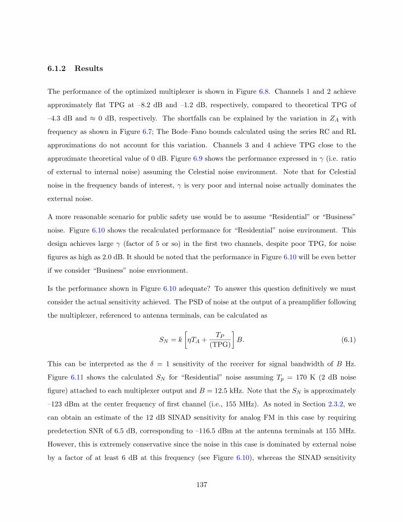
6.1.2 Results
The performance of the optimized multiplexer is shown in Figure 6.8. Channels 1 and 2 achieve
approximately flat TPG at –8.2 dB and –1.2 dB, respectively, compared to theoretical TPG of
–4.3 dB and ≈ 0 dB, respectively. The shortfalls can be explained by the variation in ZA with
frequency as shown in Figure 6.7; The Bode–Fano bounds calculated using the series RC and RL
approximations do not account for this variation. Channels 3 and 4 achieve TPG close to the
approximate theoretical value of 0 dB. Figure 6.9 shows the performance expressed in γ (i.e. ratio
of external to internal noise) assuming the Celestial noise environment. Note that for Celestial
noise in the frequency bands of interest, γ is very poor and internal noise actually dominates the
external noise.
A more reasonable scenario for public safety use would be to assume “Residential” or “Business”
noise. Figure 6.10 shows the recalculated performance for “Residential” noise environment. This
design achieves large γ (factor of 5 or so) in the first two channels, despite poor TPG, for noise
figures as high as 2.0 dB. It should be noted that the performance in Figure 6.10 will be even better
if we consider “Business” noise envrionment.
Is the performance shown in Figure 6.10 adequate? To answer this question definitively we must
consider the actual sensitivity achieved. The PSD of noise at the output of a preamplifier following
the multiplexer, referenced to antenna terminals, can be calculated as
SN = k
[ηTA +
TP
(TPG)
]B. (6.1)
This can be interpreted as the δ = 1 sensitivity of the receiver for signal bandwidth of B Hz.
Figure 6.11 shows the calculated SN for “Residential” noise assuming Tp = 170 K (2 dB noise
figure) attached to each multiplexer output and B = 12.5 kHz. Note that the SN is approximately
–123 dBm at the center frequency of first channel (i.e., 155 MHz). As noted in Section 2.3.2, we
can obtain an estimate of the 12 dB SINAD sensitivity for analog FM in this case by requiring
predetection SNR of 6.5 dB, corresponding to –116.5 dBm at the antenna terminals at 155 MHz.
However, this is extremely conservative since the noise in this case is dominated by external noise
by a factor of at least 6 dB at this frequency (see Figure 6.10), whereas the SINAD sensitivity
137
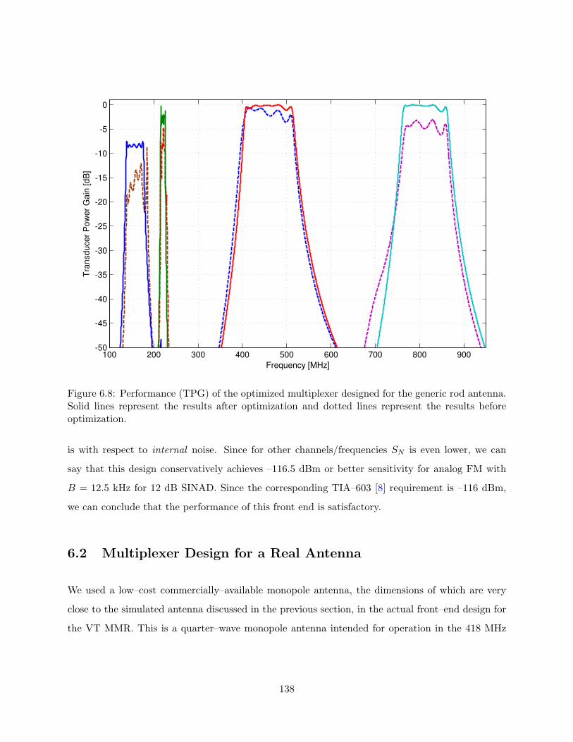
100 200 300 400 500 600 700 800 900-50
-45
-40
-35
-30
-25
-20
-15
-10
-5
0
Frequency [MHz]
Tra
nsducer
Pow
er
Gain
[dB
]
Figure 6.8: Performance (TPG) of the optimized multiplexer designed for the generic rod antenna.Solid lines represent the results after optimization and dotted lines represent the results beforeoptimization.
is with respect to internal noise. Since for other channels/frequencies SN is even lower, we can
say that this design conservatively achieves –116.5 dBm or better sensitivity for analog FM with
B = 12.5 kHz for 12 dB SINAD. Since the corresponding TIA–603 [8] requirement is –116 dBm,
we can conclude that the performance of this front end is satisfactory.
6.2 Multiplexer Design for a Real Antenna
We used a low–cost commercially–available monopole antenna, the dimensions of which are very
close to the simulated antenna discussed in the previous section, in the actual front–end design for
the VT MMR. This is a quarter–wave monopole antenna intended for operation in the 418 MHz
138
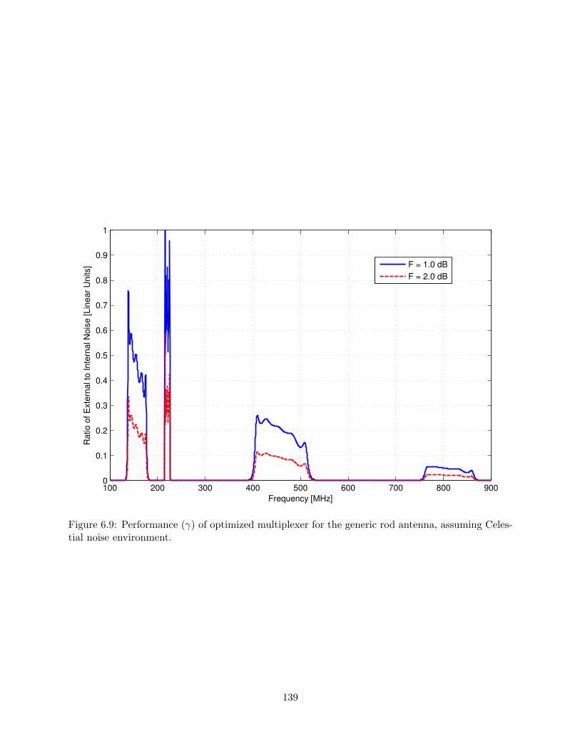
100 200 300 400 500 600 700 800 9000
0.1
0.2
0.3
0.4
0.5
0.6
0.7
0.8
0.9
1
Frequency [MHz]
Ratio o
f E
xte
rnal to
Inte
rnal N
ois
e [Lin
ear
Units]
F = 1.0 dB
F = 2.0 dB
Figure 6.9: Performance (γ) of optimized multiplexer for the generic rod antenna, assuming Celes-tial noise environment.
139

100 200 300 400 500 600 700 800 9000
2
4
6
8
10
12
14
16
18
20
Frequency [MHz]
Ratio o
f E
xte
rnal to
Inte
rnal N
ois
e [Lin
ear
Units]
F = 1.0 dB
F = 2.0 dB
Figure 6.10: Performance (γ) of the optimized multiplexer for the generic rod antenna, assuming“Residential” noise environment.
140

100 200 300 400 500 600 700 800 900-150
-145
-140
-135
-130
-125
-120
-115
-110
-105
-100
Frequency [MHz]
Nois
e P
SD
[dB
m/R
BW
],R
BW
=12.5
kH
z
Figure 6.11: Noise PSD at the output of the preamplifier referenced to antenna terminals (rodantenna). Assuming “Residential” noise as external noise source and a preamplifier with 2 dBnoise figure.
141
frequency band, Model ANT-418-CW-QW from Antenna Factor, Inc.1. The electrical specifications
from the manufacturer are 418 MHz center frequency, typical VSWR < 1.9 at center frequency,
80 MHz bandwidth, and 50Ω impedance. Figure 6.12 shows the exact dimensions of this antenna.
The measured impedance and IME are shown in Figures 6.13 and 6.14, respectively. It should
be noted that the impedance bandwidth of this commercial antenna is smaller compared to the
generic rod antenna described in the previous section. For example, for –3 dB IME the generic rod
antenna achieves approximately 282 MHz bandwidth, whereas this commercial antenna achieves
approximately 175 MHz. The next section describes the optimization of multiplexer channels for
this antenna.
6.2.1 Optimization
The maximum theoretical TPG calculated from the Bode–Fano limit using the series RC and series
RL approximations of the impedance of this antenna is shown in Table 6.4. Figure 6.15 shows the
antenna impedance calculated from the series RC and series RL approximations of the antenna
for each of the multiplexer channel frequency ranges. The maximum theoretical TPG is −1.4 dB
for the first channel and approximately 0 dB for other channels. Note that this TPG is calculated
for a matching circuit with 5th order Chebyshev topology. Following the methodology described
in Section 5.3, multiplexer channels are optimized. Since the original 5th order Chebyshev filters
was designed assuming 0.5 dB ripple, initially ε was chosen 0.5 dB for all channels. However, to
converge the optimization the values of ε were changed to 2 dB, 3 dB, 1 dB, and 3 dB for Channels
1, 2, 3, and 4, respectively. Table 6.5 shows the component values after optimization.
6.2.2 Results
The performance of the multiplexer expressed in TPG is shown in Figure 6.16. Channels 1 and 2
achieve approximately flat TPG around –6.5 dB and –2.0 dB, respectively, compared to theoretical
maximum TPG of –1.4 dB and ≈ 0 dB, respectively. The Bode-Fano bound calculated using series
RC and RL approximation (shown in Figure 6.15) is for center frequency only and do not include1http://www.antennafactor.com
142
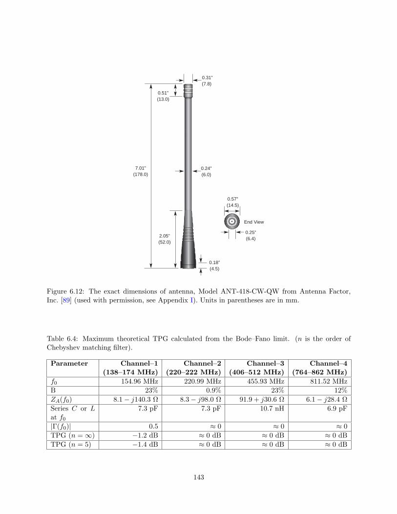
ANT-418-CW-QW DATA SHEET
Product Dimensions Description
Features
Electrical Specifications
Ordering Information
* Requires proximity ground plane
Electrical specifications and plots measured on 4.00”x 4.00” reference ground plane
CENTER 418.000MHz SPAN 200.000MHz
S11 SWR 1.158
7.01”(178.0)
0.24”(6.0)
0.51”(13.0)
2.05”(52.0)
0.18”(4.5)
0.31”(7.8)
0.25”(6.4)
End View
0.57”(14.5)
CW Series 1/4-wave antennas deliver outstandingperformance in a rugged and cosmetically attractivepackage. These antennas feature an FCC Part 15 compliantRP-SMA connector. This simplifies packaging and shipment,allowing for easy field replacement while complying withFCC requirements. A wide variety of matching connectorsallows for numerous mounting options.
Rev 07-22-08
Typical VSWR
Antenna Factor 159 Ort Lane Merlin, OR 97532 www.antennafactor.com541-956-0931 (phone) 541-471-6251 (fax)
VSWR Graph
• Low cost• Excellent performance• Omni-directional pattern• Wide bandwidth• Very low VSWR• Fully weatherized• Flexible main shaft• Rugged & damage-resistant• Part 15 compliant RP-SMA connector• Use with plastic* or metal enclosures
• Center Freq. 418MHz• Bandwidth 80MHz• Wavelength 1/4-wave• VSWR <1.9 typ. at center• Impedance 50 ohms• Connector RP-SMA
• ANT-418-CW-QW
Figure 6.12: The exact dimensions of antenna, Model ANT-418-CW-QW from Antenna Factor,Inc. [89] (used with permission, see Appendix I). Units in parentheses are in mm.
Table 6.4: Maximum theoretical TPG calculated from the Bode–Fano limit. (n is the order ofChebyshev matching filter).
Parameter Channel–1 Channel–2 Channel–3 Channel–4(138–174 MHz) (220–222 MHz) (406–512 MHz) (764–862 MHz)
f0 154.96 MHz 220.99 MHz 455.93 MHz 811.52 MHzB 23% 0.9% 23% 12%ZA(f0) 8.1− j140.3 Ω 8.3− j98.0 Ω 91.9 + j30.6 Ω 6.1− j28.4 ΩSeries C or Lat f0
7.3 pF 7.3 pF 10.7 nH 6.9 pF
|Γ(f0)| 0.5 ≈ 0 ≈ 0 ≈ 0TPG (n = ∞) −1.2 dB ≈ 0 dB ≈ 0 dB ≈ 0 dBTPG (n = 5) −1.4 dB ≈ 0 dB ≈ 0 dB ≈ 0 dB
143

100 200 300 400 500 600 700 800 9000
50
100
150R
eal Z
A [
Ω]
Frequency [MHz]
100 200 300 400 500 600 700 800 900-250
-200
-150
-100
-50
0
50
Frequency [MHz]
Imag Z
A [
Ω]
Figure 6.13: Measured impedance of antenna, Model ANT-418-CW-QW from Antenna Factor, Inc.
Table 6.5: Original and nearest standard component values of the multiplexer optimized for theantenna, Model ANT-418-CW-QW from Antenna Factor, Inc.
Component Channel–1 Channel–2 Channel–3 Channel–4Orig. Std. Orig. Std. Orig. Std. Orig. Std.
L1 (nH) 307.3 306.0 1352.5 1350.0 121.5 120.0 133.5 130.0C1 (pF) 5.4 5.4 0.4 0.4 1.1 1.1 0.3 0.3L2 (nH) 7.7 7.8 1.3 1.3 3.2 3.1 1.0 1.2C2 (pF) 140.0 139.0 404.6 399.0 38.1 39.0 39.1 33.8L3 (nH) 426.2 426.0 2032.9 2027.0 174.1 175.0 181.5 178.0C3 (pF) 2.5 2.5 0.3 0.3 0.7 0.7 0.2 0.2L4 (nH) 9.1 9.0 1.3 1.3 3.1 3.1 1.0 1.2C4 (pF) 117.5 118.0 393.1 393.0 38.9 39.0 37.7 33.7L5 (nH) 246.1 246.0 1379.4 1380.0 110.7 110.0 107.9 105.6C5 (pF) 4.3 4.3 0.4 0.4 1.1 1.1 0.4 0.4
144

100 200 300 400 500 600 700 800 900-20
-18
-16
-14
-12
-10
-8
-6
-4
-2
0
Frequency [MHz]
Impedance M
ism
atc
h E
ffic
iency [dB
]
Figure 6.14: Calculated IME between the antenna, Model ANT-418-CW-QW from Antenna Factor,Inc., and a preamplifier with Zp = 50Ω using the measured antenna impedance.
any frequency variation. This might be the reason behind the TPG difference mentioned above. On
the other hand, Channel 3 achieved TPG of –1 dB, which is close to the approximate theoretical
value of ≈ 0 dB. On the other hand, Channel 4 achieved –5.5 dB compared to the theoretical
value of ≈ 0 dB. However, this degradation of TPG does not have that much effect on the overall
sensitivity for this channel. This can be explained using Figures 6.11 and 6.19. As we notice from
the figures that for this antenna the SN calculated at the center frequency of the Channel 4 (i.e.,
811 MHz) is increased to –134.5 dBm compared to the previous value of –136.5 dBm. So the
degradation of TPG actually makes the sensitivity worse only by 2 dB.
Figure 6.17 shows the performance expressed in γ for Celestial noise environment. γ is very poor
and internal noise actually dominates the external noise in this case. Figure 6.18 shows the same
analysis for “Residential” noise. In this case we achieve large γ (factor of 5 or so) in the first
two channels, despite poor TPG, for preamplifier noise figure as high as 2.0 dB. Channel 3 and
4 are clearly not external noise–dominated in this case. It should be noted that the TPG for the
fourth channel is poor compared to the TPG calculated for the generic rod antenna. The reason
145
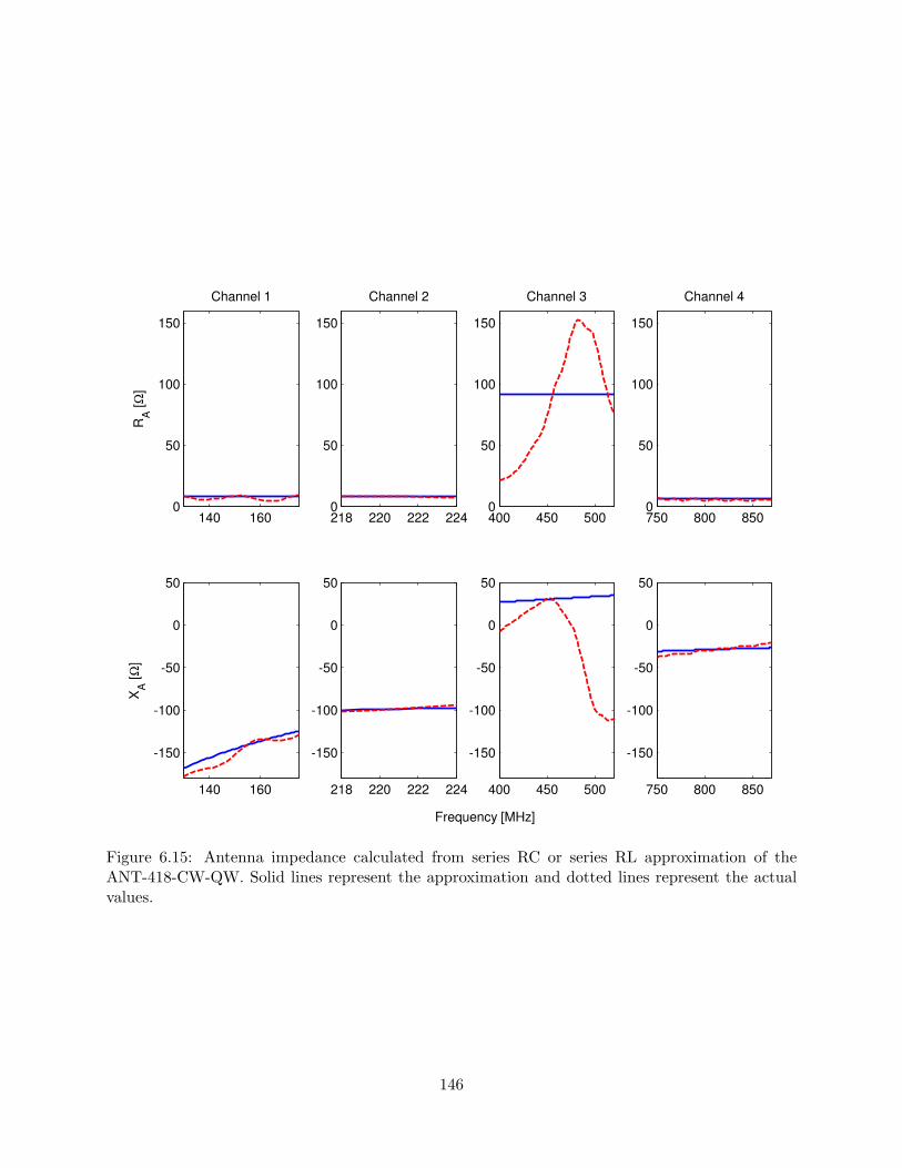
140 1600
50
100
150
Channel 1
RA [
Ω]
218 220 222 2240
50
100
150
Channel 2
400 450 5000
50
100
150
Channel 3
750 800 8500
50
100
150
Channel 4
140 160
-150
-100
-50
0
50
XA [
Ω]
218 220 222 224
-150
-100
-50
0
50
400 450 500
-150
-100
-50
0
50
Frequency [MHz]
750 800 850
-150
-100
-50
0
50
Figure 6.15: Antenna impedance calculated from series RC or series RL approximation of theANT-418-CW-QW. Solid lines represent the approximation and dotted lines represent the actualvalues.
146

behind this might be the smaller impedance bandwidth of this antenna compared to the generic
rod antenna.
To assess whether this performance is adequate in the public safety application, Figure 6.19 shows
the PSD of total noise at the output of a preamplifier with 2 dB noise figure referenced to the
antenna terminals (i.e., SN ) with B = 12.5 kHz. Note that the SN is approximately –123.5 dBm
at the center frequency of the first channel (i.e., 155 MHz). We can obtain an estimate of the
12 dB SINAD sensitivity for analog FM in this case by requiring predetection SNR of 6.5 dB,
corresponding to –117.0 dBm at the antenna terminals at 155 MHz. However, this is extremely
conservative since the noise in this case is dominated by external noise by a factor of at least
7 dB at this frequency (see Figure 6.18), whereas the SINAD sensitivity is with respect to internal
noise. Since for other channels/frequencies SN is even lower, we can say that this design achieved
–117.0 dBm or better sensitivity (typical value is –116 dBm [8]) for analog FM with B = 12.5 kHz
for 12 dB SINAD. As a result we can conclude that the performance of this front end is satisfactory.
6.2.3 Implementation and Lab Results
This multiplexer was designed and fabricated as a four–layer printed circuit board (PCB), the
details of which are presented in Appendix E. (The assembled multiplexer board is shown in Fig-
ure 7.13.) The S21 parameter of each of the channels using 50Ω termination was measured and
compared with the S21 calculated from the simulation results using the same termination (instead
of antenna impedance). Figure 6.20 shows the results assuming 50Ω source and load impedance.
The performance of the implemented multiplexer is worse (especially Channels 2–4) compared to
the simulated performance. In particular the performance of Channel 4 is completely unaccept-
able. This is mainly for two reasons: (1) Due to the parasitic effects from the PCB layout, and (2)
Because suitable standard components are not available. In our application inductors with high Q
(100 or higher) and high series resonant frequency (SRF) (higher than 1 GHz) are needed. Similarly
it is desired to have capacitors with high Q (10,000 or higher) and low equivalent series resistance
(ESR) (possibly 0Ω). However, “Q” of the inductors we used are between 12 to 25, and many of
them has SRF below 700 MHz (the frequency of which falls into our desired frequency bands). On
the other hand, Q of the capacitors we used in the range of 100 to 1000, and ESR is in the range
147

of 0.2 to 0.5 Ω.
As we mentioned in the previous chapter, this problem might be improved by including the effects
of board parasitics (from PCB) during the simulation of this multiplexer. Moreover, trimmer
capacitors can be used to perform fine adjustments to the components. Since the frequency range
of channel 4 is close to GHz range, we might consider using microstrip type of design to implement
this channel. So the combination of using microstrip and passive components can be an alternative
approach for implementing this multiplexer. However, due to schedule and funding limitations we
did not able to experiment with this.
We were unable to obtain TPG from the S21 results shown in Figure 6.20, because the S21 mea-
surement were scalar (magnitude–only) opposed to coherent (magnitude and phase). We were
also unable to make a validating field measurement using Celestial noise, as Celestial noise is far
too weak in this frequency regime to be detectable using the simple equipment available in Chap-
ter 4 and 5. Thus, the best estimate of “bottom line” performance for this antenna–multiplexer
combination, assuming suitable components can be found, is as shown in Figures 6.16–6.18.
6.3 Summary
This chapter described the design of two multiplexers for application in public safety MMR as
discussed in Section 1.2. The first multiplexer was designed for a generic rod antenna. The TPG
performance of this multiplexer closely follows the theoretical (approximate series RC/RL based)
Bode–Fano limit. The second multiplexer was designed for an actual commercial monopole antenna
of similar length and radius. Although the TPG performance of this multiplexer is not as good as
the previous one (especially Channel 4), this has only a slight effect (less than 2 dB degradation)
on sensitivity. In both cases γ (i.e., the ratio of external noise to internal noise) is a factor of
5 or so, and sensitivity is –116.5 dBm or better (for B = 12.5 kHz and 12 dB SINAD) for a
preamplifier noise figure of 2 dB. Although simulation results indicate satisfactory performance for
all four channels, due to the parasitic effects of the PC board and lack of suitable components, the
constructed multiplexer does not exhibit acceptable performance.
A complete description of the VT MMR is provided in the next chapter.
148
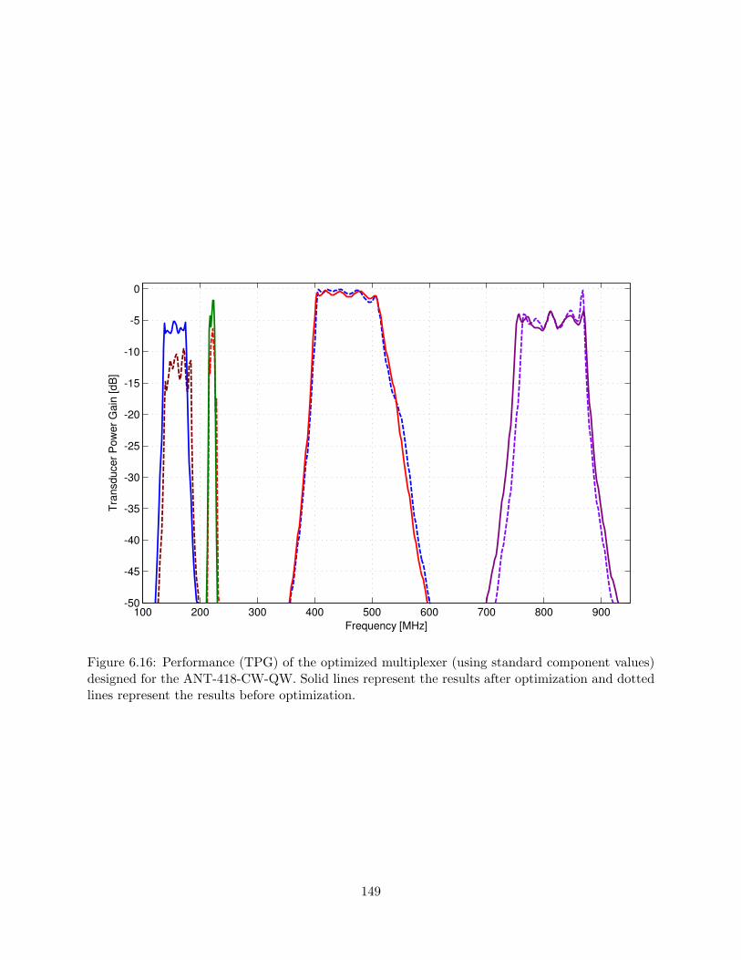
100 200 300 400 500 600 700 800 900-50
-45
-40
-35
-30
-25
-20
-15
-10
-5
0
Frequency [MHz]
Tra
nsducer
Pow
er
Gain
[dB
]
Figure 6.16: Performance (TPG) of the optimized multiplexer (using standard component values)designed for the ANT-418-CW-QW. Solid lines represent the results after optimization and dottedlines represent the results before optimization.
149
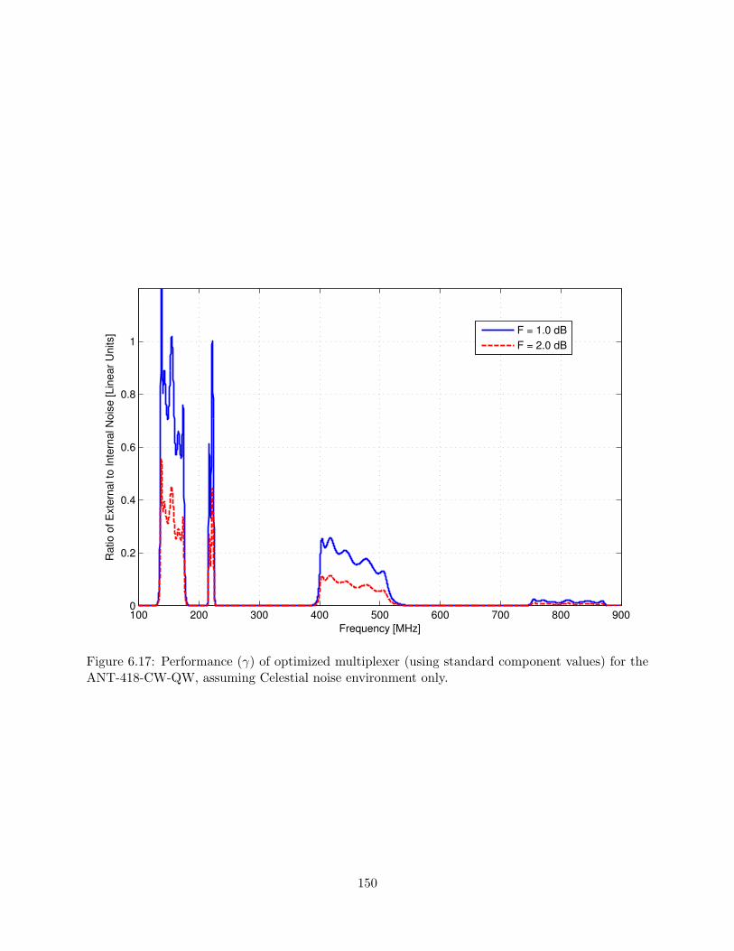
100 200 300 400 500 600 700 800 9000
0.2
0.4
0.6
0.8
1
Frequency [MHz]
Ratio o
f E
xte
rnal to
Inte
rnal N
ois
e [Lin
ear
Units]
F = 1.0 dB
F = 2.0 dB
Figure 6.17: Performance (γ) of optimized multiplexer (using standard component values) for theANT-418-CW-QW, assuming Celestial noise environment only.
150

100 200 300 400 500 600 700 800 9000
5
10
15
20
25
Frequency [MHz]
Ratio o
f E
xte
rnal to
Inte
rnal N
ois
e [Lin
ear
Units]
F = 1.0 dB
F = 2.0 dB
Figure 6.18: Performance (γ) of optimized multiplexer (using standard component values) for theANT-418-CW-QW, assuming “Residential” noise environment.
151
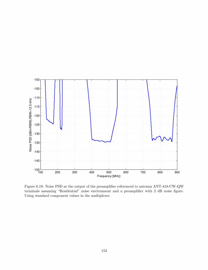
100 200 300 400 500 600 700 800 900-150
-145
-140
-135
-130
-125
-120
-115
-110
-105
-100
Frequency [MHz]
Nois
e P
SD
[dB
m/R
BW
],R
BW
=12.5
kH
z
Figure 6.19: Noise PSD at the output of the preamplifier referenced to antenna ANT-418-CW-QWterminals assuming “Residential” noise environment and a preamplifier with 2 dB noise figure.Using standard component values in the multiplexer.
152

100 200 300 400 500 600 700 800 900-40
-35
-30
-25
-20
-15
-10
-5
0
Frequency [MHz]
Tra
nsducer
Pow
er
Gain
[dB
]
Figure 6.20: Lab measurement of the optimized (using standard component values given inTable 6.5) multiplexer designed for the ANT-418-CW-QW, using instead 50Ω source and loadimpedances. Solid lines represent the measurement results and dashed lines are the results fromsimulation. (Note that this result is not representative of actual performance, since the sourceimpedance is 50Ω as opposed to ZA).
153

Chapter 7
Design & Development of a
Multiband Multimode Radio
This chapter presents the design and development of a MMR for public safety applications, which
provides the opportunity to demonstrate the sensitivity–constrained RF multiplexer design concept
(Sections 5.3 and 6.2) using direct conversion architecture (Section 2.4.3). Figure 7.1 shows the
VT MMR prototype. This chapter is organized as follows. Section 7.1 (“Overview of the Project”)
presents a brief overview of the VT MMR project. An early design concept for this radio is presented
in Section 7.2 (“Original Superhet Architecture”). Then the availability of a CMOS–based direct
conversion RFIC motivated us to modify the architecture. An overview and performance analysis
of this RFIC is presented in Section 7.3 (“Motorola RFIC: Description & Performance Analysis”).
Section 7.4 (“Direct Conversion Architecture”) describes the architecture developed using the new
RFIC. A description of the developed prototype is presented in Section 7.5 (“Prototype Design”).
This chapter is summarized in Section 7.6 (“Summary”).
154
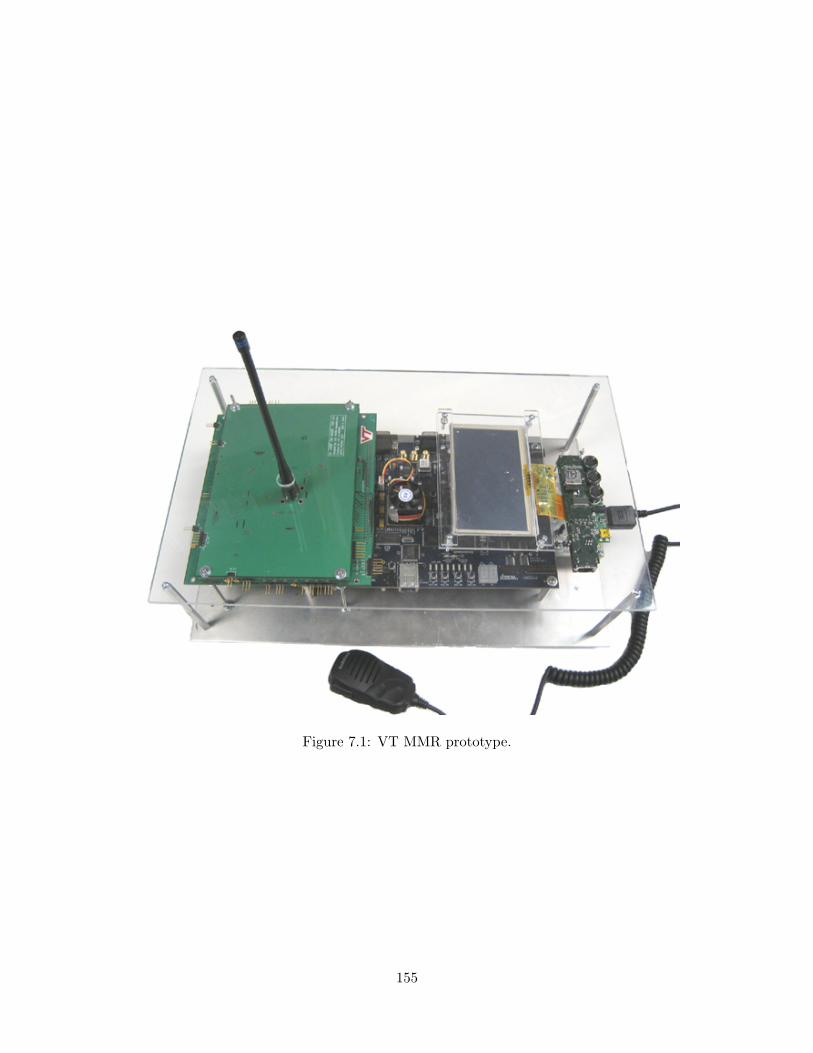
Figure 7.1: VT MMR prototype.
155

7.1 Overview of the Project
At Virginia Tech, we are working to develop a MMR to solve the interoperability issues among the
public safety organizations1. This issue has already been discussed in Section 1.2 (“Application
Example: Public Safety”). We are working to develop a radio which would be able to communicate
in any public safety radio system, immediately and without prior technical coordination. This
research is part of a project sponsored by the U.S. Department of Justice [90, 91].
The goal of the VT MMR project is to develop and demonstrate a single radio which can operate
in the frequency bands shown in Table 1.1 using any mode; and be able to operate on multiple
frequency bands simultaneously. It should be noted that following guidance from the sponsor, it
was decided to limit the frequency range of interest to bands above 100 MHz; i.e., not to include
the VHF low band (25–50 MHz). Also, for reasons to be discussed in Section 7.2, we decided to
focus our attention on bands below 1 GHz. Thus, the total frequency range of interest is from 138
MHz to 862 MHz.
Table 7.1 shows the sensitivity requirement from the standards document TIA–603 [8] for analog
FM communication below 1 GHz. It also shows for comparison the performance of the final VT
MMR (Section 7.5) as well as the performance of other currently available MMRs with similar
design goals.
7.2 Original Superhet Architecture
Figure 7.2 shows the initial strawman design of the VT MMR, which was a more traditional design
based on the “divide–and–conquer” superhet architecture. It is noticeable from Table 1.1 that the
spectrum used for public safety applications below 1 GHz is relatively concentrated into just a
few, relatively narrow but contiguous “chunks” of spectrum; namely “VHF” (138–174 and 220–222
MHz), “UHF” (406–512 MHz), and the 700 MHz and 800 MHz bands. Bands above 1 GHz do not
use the same narrowband voice modes prevalent below 1 GHz, but rather use cellular protocols
(around 1900 MHz), unlicensed spectrum around 2.4 GHz using IEEE 802.11 modes (Wi–Fi), and1VT MMR Project Website: http://www.ece.vt.edu/swe/chamrad/
156
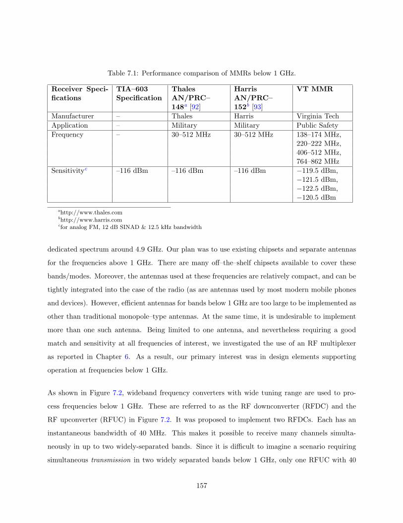
Table 7.1: Performance comparison of MMRs below 1 GHz.
Receiver Speci-fications
TIA–603Specification
ThalesAN/PRC–148a [92]
HarrisAN/PRC–152b [93]
VT MMR
Manufacturer – Thales Harris Virginia TechApplication – Military Military Public SafetyFrequency – 30–512 MHz 30–512 MHz 138–174 MHz,
220–222 MHz,406–512 MHz,764–862 MHz
Sensitivityc –116 dBm –116 dBm –116 dBm −119.5 dBm,−121.5 dBm,−122.5 dBm,−120.5 dBm
ahttp://www.thales.combhttp://www.harris.comcfor analog FM, 12 dB SINAD & 12.5 kHz bandwidth
dedicated spectrum around 4.9 GHz. Our plan was to use existing chipsets and separate antennas
for the frequencies above 1 GHz. There are many off–the–shelf chipsets available to cover these
bands/modes. Moreover, the antennas used at these frequencies are relatively compact, and can be
tightly integrated into the case of the radio (as are antennas used by most modern mobile phones
and devices). However, efficient antennas for bands below 1 GHz are too large to be implemented as
other than traditional monopole–type antennas. At the same time, it is undesirable to implement
more than one such antenna. Being limited to one antenna, and nevertheless requiring a good
match and sensitivity at all frequencies of interest, we investigated the use of an RF multiplexer
as reported in Chapter 6. As a result, our primary interest was in design elements supporting
operation at frequencies below 1 GHz.
As shown in Figure 7.2, wideband frequency converters with wide tuning range are used to pro-
cess frequencies below 1 GHz. These are referred to as the RF downconverter (RFDC) and the
RF upconverter (RFUC) in Figure 7.2. It was proposed to implement two RFDCs. Each has an
instantaneous bandwidth of 40 MHz. This makes it possible to receive many channels simulta-
neously in up to two widely-separated bands. Since it is difficult to imagine a scenario requiring
simultaneous transmission in two widely separated bands below 1 GHz, only one RFUC with 40
157
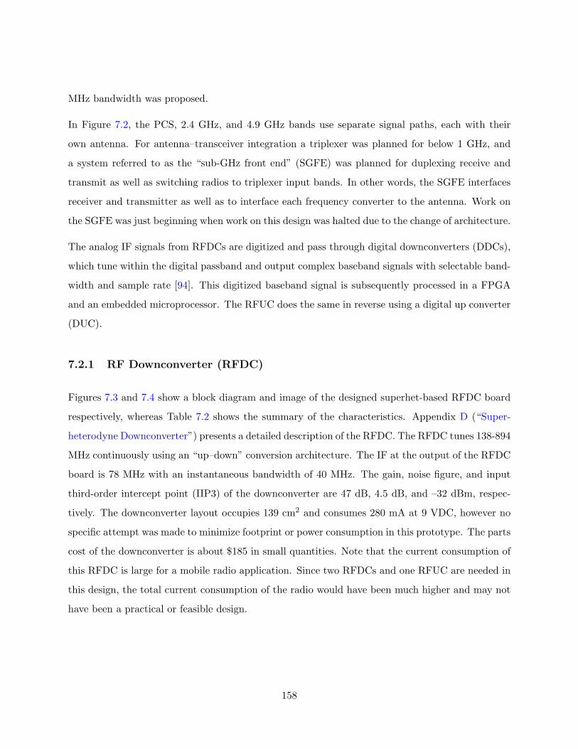
MHz bandwidth was proposed.
In Figure 7.2, the PCS, 2.4 GHz, and 4.9 GHz bands use separate signal paths, each with their
own antenna. For antenna–transceiver integration a triplexer was planned for below 1 GHz, and
a system referred to as the “sub-GHz front end” (SGFE) was planned for duplexing receive and
transmit as well as switching radios to triplexer input bands. In other words, the SGFE interfaces
receiver and transmitter as well as to interface each frequency converter to the antenna. Work on
the SGFE was just beginning when work on this design was halted due to the change of architecture.
The analog IF signals from RFDCs are digitized and pass through digital downconverters (DDCs),
which tune within the digital passband and output complex baseband signals with selectable band-
width and sample rate [94]. This digitized baseband signal is subsequently processed in a FPGA
and an embedded microprocessor. The RFUC does the same in reverse using a digital up converter
(DUC).
7.2.1 RF Downconverter (RFDC)
Figures 7.3 and 7.4 show a block diagram and image of the designed superhet-based RFDC board
respectively, whereas Table 7.2 shows the summary of the characteristics. Appendix D (“Super-
heterodyne Downconverter”) presents a detailed description of the RFDC. The RFDC tunes 138-894
MHz continuously using an “up–down” conversion architecture. The IF at the output of the RFDC
board is 78 MHz with an instantaneous bandwidth of 40 MHz. The gain, noise figure, and input
third-order intercept point (IIP3) of the downconverter are 47 dB, 4.5 dB, and –32 dBm, respec-
tively. The downconverter layout occupies 139 cm2 and consumes 280 mA at 9 VDC, however no
specific attempt was made to minimize footprint or power consumption in this prototype. The parts
cost of the downconverter is about $185 in small quantities. Note that the current consumption of
this RFDC is large for a mobile radio application. Since two RFDCs and one RFUC are needed in
this design, the total current consumption of the radio would have been much higher and may not
have been a practical or feasible design.
158
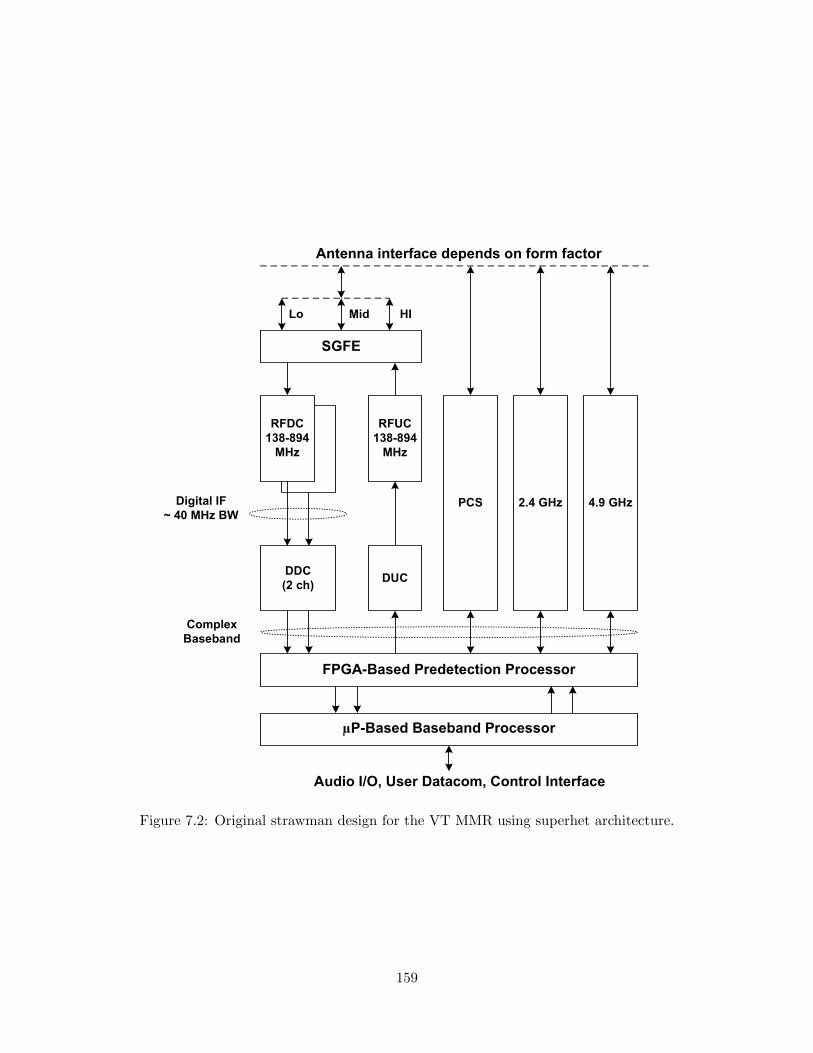
SGFE
RFDC
138-894
MHz
RFUC
138-894
MHz
PCS 2.4 GHz 4.9 GHz
DDC
(2 ch)DUC
FPGA-Based Predetection Processor
µP-Based Baseband Processor
Audio I/O, User Datacom, Control Interface
Lo Mid HI
Antenna interface depends on form factor
Digital IF
~ 40 MHz BW
Complex
Baseband
Figure 7.2: Original strawman design for the VT MMR using superhet architecture.
159

Low Level Diagram of RF Down-Converter for the NIJ Project
This design is for 5 frequency bands, Version 2.0
Frequency Bands:
High: 746-776
Mid: 450-512
Low: 138-222
DIPLEXER
1250 MHz
DIPLEXER
78 MHz1220-1280 MHz 58-98 MHz
1388-2144 MHz 1328 MHz
TO
ADC
FROM
PRESELECTOR
1220-1280 MHz
(138-894 MHz)
1250 MHz IF 78 MHz IF
Figure 7.3: Block diagram of the superhet–based RF downconverter designed for the VT MMR.
Table 7.2: Characteristics summary of the RF downconverter designed for the original (superhet–based) VT MMR.
Parameter Measured Performance UnitsTuning Range 138–894 (continuous) MHzInstantaneous 3 dB Bandwidth 40.0 MHz
Gain50.5 (max.)
dB47.0 (avg.)35.4 (min.)
IIP3
–28.0 (max.)dBm–32.0 (avg.)
–34.0 (min.)Noise Figure 4.5 dBPower 2.52 (0.28 A @ 9.0 V) WOutput IF Center Frequency 78.0 MHzDimensions 3.5× 6.0 in
7.2.2 RF Upconverter (RFUC)
Using a similar philosophy, a superhet–based RFUC was also designed which tunes 138-894 MHz
continuously using the same frequency plan as the RFDC. Figure 7.5 shows this board. However,
the decision to change to the new architecture was made before measurements were performed for
this board, and the design was not documented in a separate report.
160
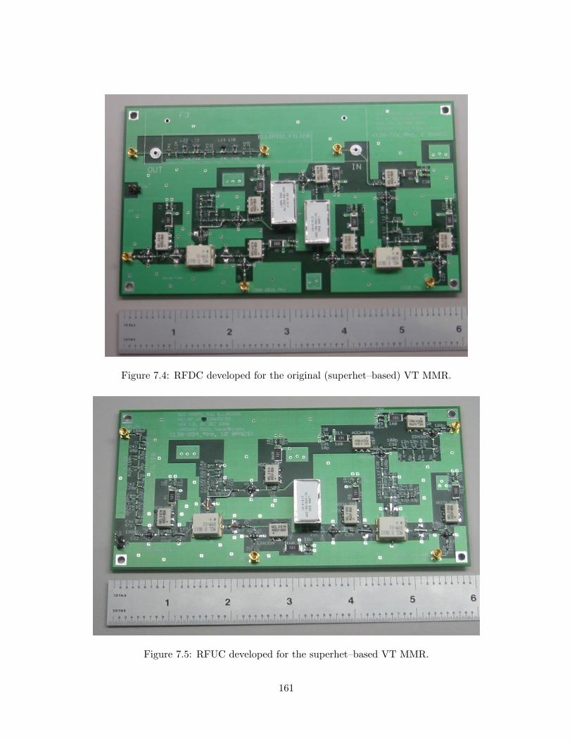
Figure 7.4: RFDC developed for the original (superhet–based) VT MMR.
Figure 7.5: RFUC developed for the superhet–based VT MMR.
161
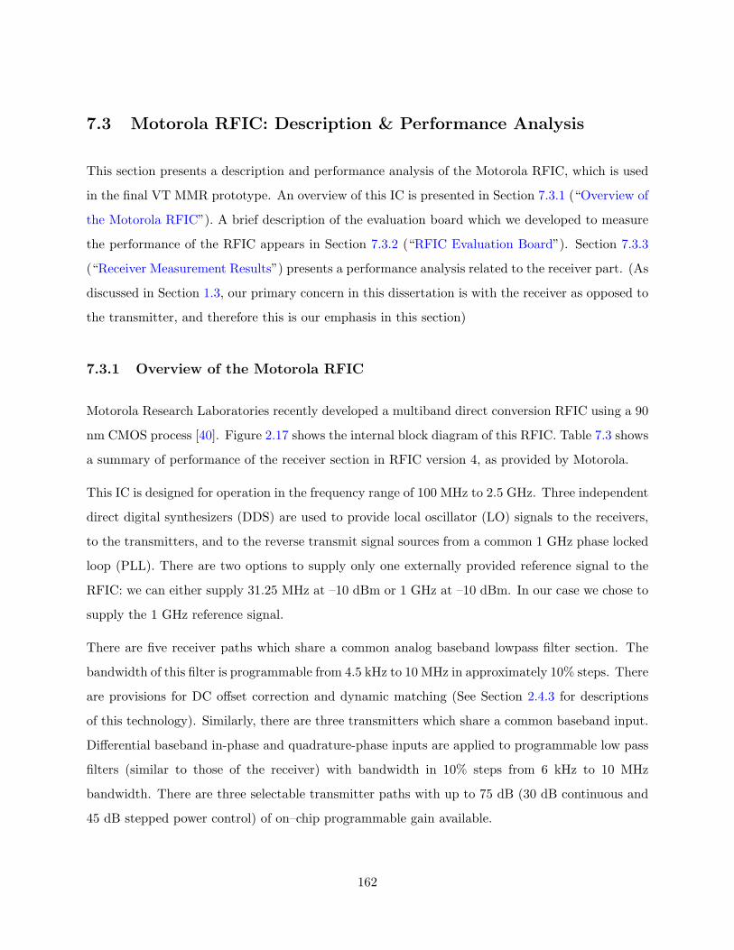
7.3 Motorola RFIC: Description & Performance Analysis
This section presents a description and performance analysis of the Motorola RFIC, which is used
in the final VT MMR prototype. An overview of this IC is presented in Section 7.3.1 (“Overview of
the Motorola RFIC”). A brief description of the evaluation board which we developed to measure
the performance of the RFIC appears in Section 7.3.2 (“RFIC Evaluation Board”). Section 7.3.3
(“Receiver Measurement Results”) presents a performance analysis related to the receiver part. (As
discussed in Section 1.3, our primary concern in this dissertation is with the receiver as opposed to
the transmitter, and therefore this is our emphasis in this section)
7.3.1 Overview of the Motorola RFIC
Motorola Research Laboratories recently developed a multiband direct conversion RFIC using a 90
nm CMOS process [40]. Figure 2.17 shows the internal block diagram of this RFIC. Table 7.3 shows
a summary of performance of the receiver section in RFIC version 4, as provided by Motorola.
This IC is designed for operation in the frequency range of 100 MHz to 2.5 GHz. Three independent
direct digital synthesizers (DDS) are used to provide local oscillator (LO) signals to the receivers,
to the transmitters, and to the reverse transmit signal sources from a common 1 GHz phase locked
loop (PLL). There are two options to supply only one externally provided reference signal to the
RFIC: we can either supply 31.25 MHz at –10 dBm or 1 GHz at –10 dBm. In our case we chose to
supply the 1 GHz reference signal.
There are five receiver paths which share a common analog baseband lowpass filter section. The
bandwidth of this filter is programmable from 4.5 kHz to 10 MHz in approximately 10% steps. There
are provisions for DC offset correction and dynamic matching (See Section 2.4.3 for descriptions
of this technology). Similarly, there are three transmitters which share a common baseband input.
Differential baseband in-phase and quadrature-phase inputs are applied to programmable low pass
filters (similar to those of the receiver) with bandwidth in 10% steps from 6 kHz to 10 MHz
bandwidth. There are three selectable transmitter paths with up to 75 dB (30 dB continuous and
45 dB stepped power control) of on–chip programmable gain available.
162

Table 7.3: RFIC version 4 receiver performance summary, as provided by Motorola [40].
Parameter ValueFrequency Range 100 MHz – 2.5 GHzReceiver Noise Figure 7 dBReceiver Gain 48 dBReceiver IIP2 +60 dBmReceiver IIP3 –6 dBmReceiver Current Drain 40 mALO Phase Noise –123 dBc/Hz @ 25 kHzLO Frequency Resolution 15 HzLO Current Drain per DDS 80 mA
All the parameters of the RFIC can be controlled and configured using a serial port interface (SPI)
link, which consists of five signals: chip select, clock, reset, serial input, and serial output. In
order to operate this IC and to set the various parameters, a minimum of 262 registers must be
programmed through SPI.
Prior to using this RFIC in our design, we evaluated it using two separate evaluation boards.
The first evaluation board was provided by Motorola. The second evaluation board was built by
us and is described in Section 7.3.2. We found performance to be generally consistent with the
specifications published by Motorola.
7.3.2 RFIC Evaluation Board
We designed and developed an evaluation board, which contains RFIC version 4, in order to validate
Motorola’s performance specifications and to ensure that we were able to reproduce their main
results when the chip was integrated into a design developed by us. Figure 7.6 shows this evaluation
board. The design of this board fully documented in [95]. This board contains all the circuitry
needed to evaluate this IC including power circuit, SPI circuit, etc. All of the RF input/output (i.e.
receive and transmit) ports require differential signals. Since our RF front end (including filters,
preamplifiers), measurement instruments, and other related components are single–ended, we used
on–board baluns to convert single–ended signals to differential, and vice–versa in all five receive and
three transmit ports. To interface to the differential baseband ports we used two peripheral boards
163

Figure 7.6: VT evaluation board for Motorola RFIC version 4. The IC itself is the square chip inthe center of the board.
provided by Motorola: one converts a differential input signal to a single–ended output signal; and
the other board converts a single–ended signal to a differential output signal to supply baseband
input to the transmitter.
In our measurements we used a LabView4 program, which was also developed by Motorola, to
control the functionality of the RFIC via SPI. Figure 7.7 shows a screenshot of this program. The
default settings which are used during the measurement of the RFIC receiver are presented in
Table 7.4. Additional details of the testing are documented in [96].
4http://www.ni.com/labview
164
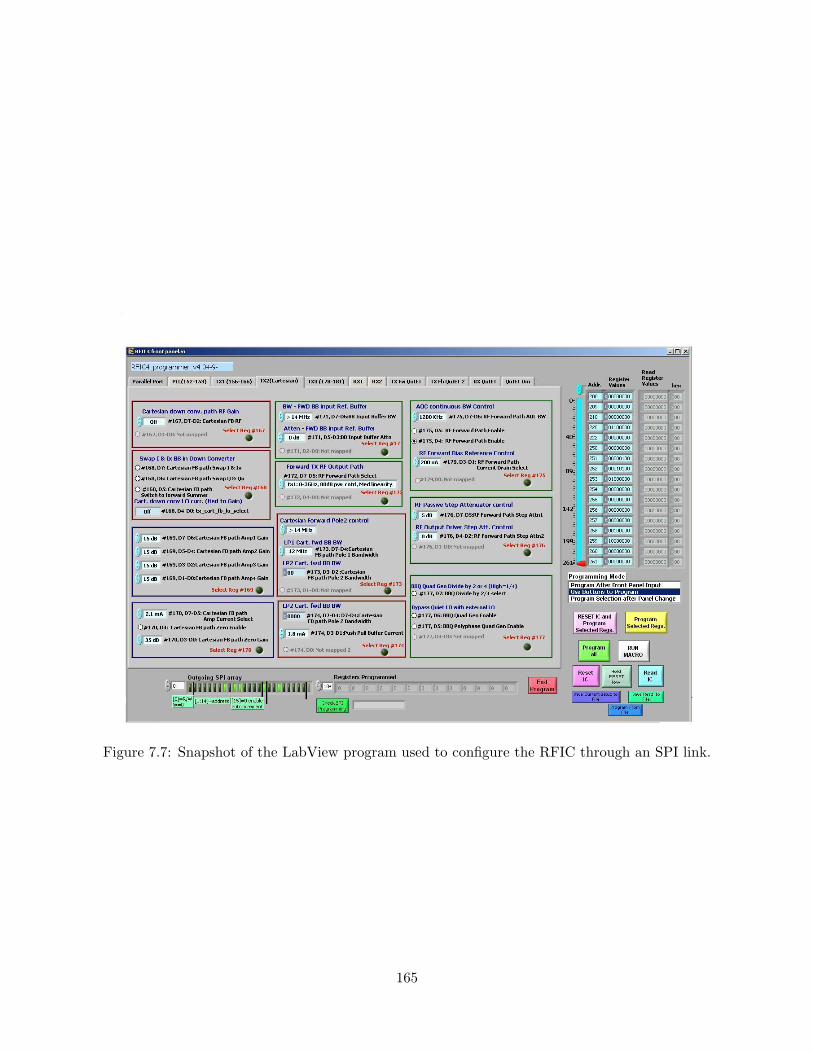
Figure 7.7: Snapshot of the LabView program used to configure the RFIC through an SPI link.
165
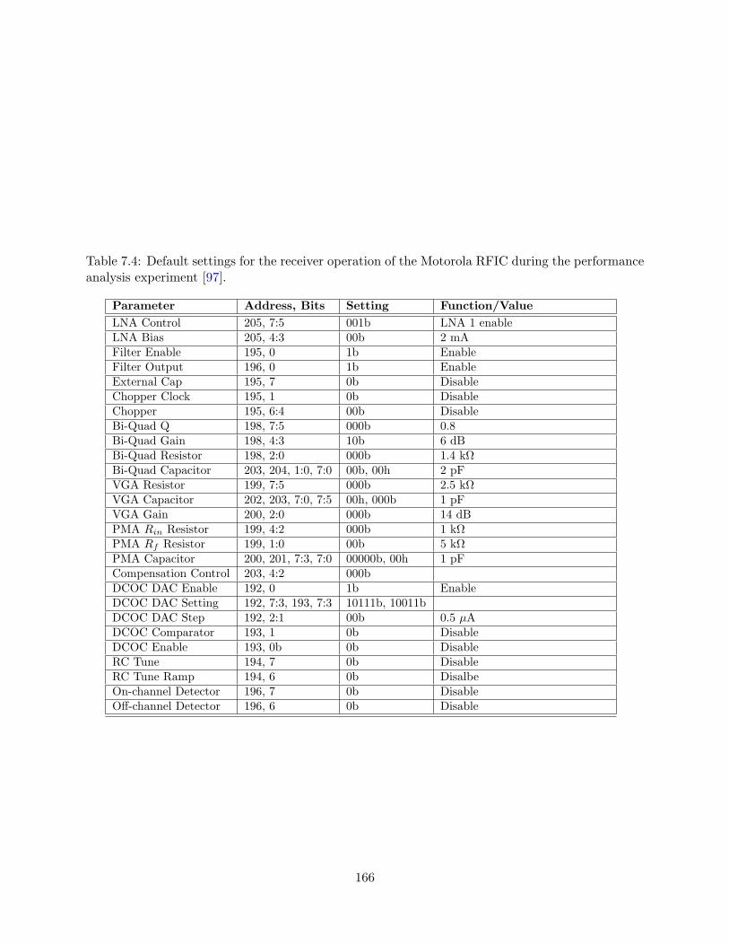
Table 7.4: Default settings for the receiver operation of the Motorola RFIC during the performanceanalysis experiment [97].
Parameter Address, Bits Setting Function/ValueLNA Control 205, 7:5 001b LNA 1 enableLNA Bias 205, 4:3 00b 2 mAFilter Enable 195, 0 1b EnableFilter Output 196, 0 1b EnableExternal Cap 195, 7 0b DisableChopper Clock 195, 1 0b DisableChopper 195, 6:4 00b DisableBi-Quad Q 198, 7:5 000b 0.8Bi-Quad Gain 198, 4:3 10b 6 dBBi-Quad Resistor 198, 2:0 000b 1.4 kΩBi-Quad Capacitor 203, 204, 1:0, 7:0 00b, 00h 2 pFVGA Resistor 199, 7:5 000b 2.5 kΩVGA Capacitor 202, 203, 7:0, 7:5 00h, 000b 1 pFVGA Gain 200, 2:0 000b 14 dBPMA Rin Resistor 199, 4:2 000b 1 kΩPMA Rf Resistor 199, 1:0 00b 5 kΩPMA Capacitor 200, 201, 7:3, 7:0 00000b, 00h 1 pFCompensation Control 203, 4:2 000bDCOC DAC Enable 192, 0 1b EnableDCOC DAC Setting 192, 7:3, 193, 7:3 10111b, 10011bDCOC DAC Step 192, 2:1 00b 0.5 µADCOC Comparator 193, 1 0b DisableDCOC Enable 193, 0b 0b DisableRC Tune 194, 7 0b DisableRC Tune Ramp 194, 6 0b DisalbeOn-channel Detector 196, 7 0b DisableOff-channel Detector 196, 6 0b Disable
166

7.3.3 Receiver Measurement Results
This section presents the RFIC receiver section measurement results using the above evaluation
board, which have been taken using the first of five receive ports of the RFIC. Table 7.5 summarizes
the receiver measurement results in public safety frequency bands. These results apply to the RFIC
without any attempt to optimize configurable settings internal to the chip.
Fig. 7.8 shows the gain–frequency characteristics. This is power gain, measured with respect to
50 Ω termination. Although the gain rolls off a little bit in the VHF and PCS bands, it is steady
in the UHF, 700 MHz and 800 MHz bands. We can see that the gain lies between 45 and 52 dB,
which is consistent with Motorola’s specification in Table 7.3.
Figure 7.9 shows the input 1 dB compression point for the RFIC receiver. The input 1 dB com-
pression point varies between –35 and –14 dBm, and it improves once we cross into the UHF band.
Although it was not measured, we can estimate the IIP3 using Equation 2.23; it varies between –25
and –4 dBm. It should be noted that the IIP3 specification provided by Motorola shown in Ta-
ble 7.3 (–6 dBm) is measured at 800 MHz. From our measurement we achieve –16 dBm IIP3 at 800
MHz which is approximately 10 dB lower than Motorola’s specification. Discussion with Motorola
suggests that this difference probably due to the associated external circuitry (e.g., balun) used in
the evaluation board [41]. However, this fact has not been confirmed due to the unavailability of
IIP3 information in the balun manufacturer’s datasheet.
The measurement results of image rejection for the RFIC receiver are shown in Figure 7.10. We
performed these measurements using the default parameters, which are optimized for 800 MHz,
and did not attempt to optimize the performance for other frequencies. For that reason, the image
rejection is high in the 800 MHz frequency band compared to the other bands. We observed
the worst image rejection with these settings is in the PCS band; approximately 9 dB. Although
presumably the performance achieved at 800 MHz could be achieved at other frequencies with some
tuning of the parameters in Table 7.4, due to schedule and funding limitations we did not attempt
to do this.
167

Table 7.5: Measured receiver performance of the RFIC in public safety frequency bands.
Band Freq. (MHz) Gain (dB) P1dB (dBm) Image Rejection (dB)
VHF156.0 47.8 −33.0 27.6221.0 49.8 −33.0 24.9
UHF 459.0 48.8 −34.0 19.4
700 MHz770.0 50.0 −27.0 28.7800.0 49.8 −26.0 30.0
800 MHz
811.5 50.1 −24.0 35.7836.5 51.0 −23.0 42.2856.5 51.1 −23.0 38.4881.5 50.6 −22.0 28.4
PCS 1920.0 42.2 −14.0 9.2010V @ 0.11A (1.1 W)a total for the evaluation board
aCurrent drain for the RFIC alone: 40 mA @ 2.5 V for RF/BB; 80 mA @ 2.5 V for LO
200 400 600 800 1000 1200 1400 1600 180030
35
40
45
50
55
60
Frequency [MHz]
Gain
[dB
]
Figure 7.8: Gain measured in the first receiver port of the RFIC.
168

200 400 600 800 1000 1200 1400 1600 1800-50
-45
-40
-35
-30
-25
-20
-15
-10
-5
Frequency [MHz]
Input 1 d
B C
om
pre
ssio
n P
oin
t [d
B]
Figure 7.9: Input 1 dB compression point measured in the first receiver port of the RFIC.
200 400 600 800 1000 1200 1400 1600 18005
10
15
20
25
30
35
40
45
Frequency [MHz]
Image R
eje
ction [dB
]
Figure 7.10: Image rejection measured in the first receiver port of the RFIC.
169
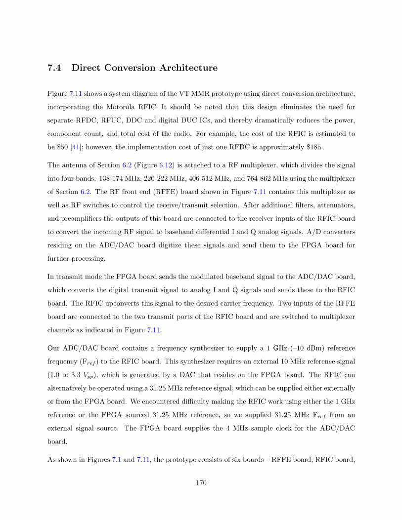
7.4 Direct Conversion Architecture
Figure 7.11 shows a system diagram of the VT MMR prototype using direct conversion architecture,
incorporating the Motorola RFIC. It should be noted that this design eliminates the need for
separate RFDC, RFUC, DDC and digital DUC ICs, and thereby dramatically reduces the power,
component count, and total cost of the radio. For example, the cost of the RFIC is estimated to
be $50 [41]; however, the implementation cost of just one RFDC is approximately $185.
The antenna of Section 6.2 (Figure 6.12) is attached to a RF multiplexer, which divides the signal
into four bands: 138-174 MHz, 220-222 MHz, 406-512 MHz, and 764-862 MHz using the multiplexer
of Section 6.2. The RF front end (RFFE) board shown in Figure 7.11 contains this multiplexer as
well as RF switches to control the receive/transmit selection. After additional filters, attenuators,
and preamplifiers the outputs of this board are connected to the receiver inputs of the RFIC board
to convert the incoming RF signal to baseband differential I and Q analog signals. A/D converters
residing on the ADC/DAC board digitize these signals and send them to the FPGA board for
further processing.
In transmit mode the FPGA board sends the modulated baseband signal to the ADC/DAC board,
which converts the digital transmit signal to analog I and Q signals and sends these to the RFIC
board. The RFIC upconverts this signal to the desired carrier frequency. Two inputs of the RFFE
board are connected to the two transmit ports of the RFIC board and are switched to multiplexer
channels as indicated in Figure 7.11.
Our ADC/DAC board contains a frequency synthesizer to supply a 1 GHz (–10 dBm) reference
frequency (Fref ) to the RFIC board. This synthesizer requires an external 10 MHz reference signal
(1.0 to 3.3 Vpp), which is generated by a DAC that resides on the FPGA board. The RFIC can
alternatively be operated using a 31.25 MHz reference signal, which can be supplied either externally
or from the FPGA board. We encountered difficulty making the RFIC work using either the 1 GHz
reference or the FPGA–sourced 31.25 MHz reference, so we supplied 31.25 MHz Fref from an
external signal source. The FPGA board supplies the 4 MHz sample clock for the ADC/DAC
board.
As shown in Figures 7.1 and 7.11, the prototype consists of six boards – RFFE board, RFIC board,
170
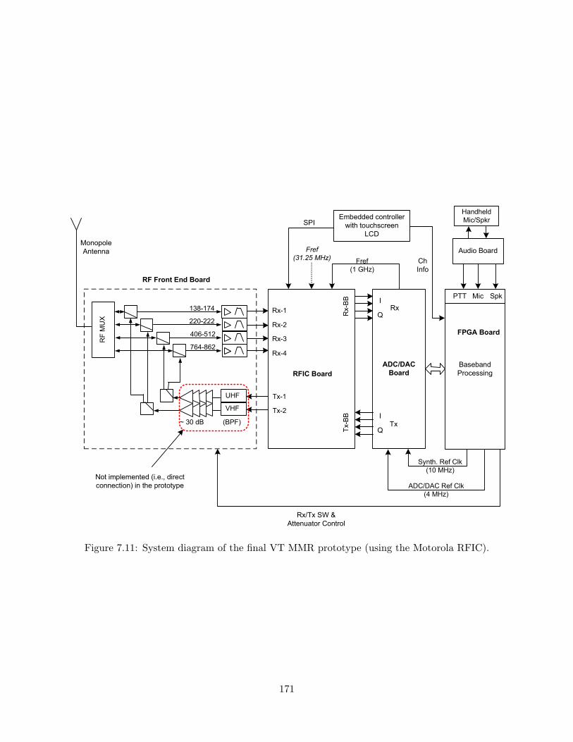
RF Front End Board
ADC/DAC
Board
Rx/Tx SW &
Attenuator Control
Rx
Tx
I
Q
I
Q
Baseband
Processing
FPGA Board
Embedded controller
with touchscreen
LCD
SPI
Audio Board
PTT Mic Spk
Ch
Info
RF MUX
138-174
220-222
406-512
764-862
UHF
VHF
(BPF)~ 30 dB
Rx-1
Rx-2
Rx-3
Rx-4
Tx-1
Tx-2
Rx-BB
Tx-BB
Fref
(1 GHz)
Handheld
Mic/Spkr
RFIC Board
Not implemented (i.e., direct
connection) in the prototype
Monopole
Antenna
ADC/DAC Ref Clk
(4 MHz)
Synth. Ref Clk
(10 MHz)
Fref
(31.25 MHz)
Figure 7.11: System diagram of the final VT MMR prototype (using the Motorola RFIC).
171

ADC/DAC board, FPGA board, audio control board, and user interface board. The first three
boards are stacked together and connected directly, i.e., without cable, using male–female MMCX
RF connectors in order to achieve a more compact arrangement. The ADC/DAC board is also
connected with the FPGA board using a 80–pin square 0.1-in header using the “Analog Devices
Interface” (ADI) pin assignment scheme. A detailed description of the audio board and the user
interface of this radio is provided in Appendix H. The next section describes the design of other
parts in more detail.
7.5 Prototype Design
This section presents the design overview of the developed VT MMR prototype. Section 7.5.1
(“RFFE Board”) and Section 7.5.2 (“RFIC Board”) describe the RFFE board and the RFIC
board, respectively. The description of the ADC/DAC board and the FPGA board is presented in
Section 7.5.3 (“ADC/DAC Board”) and Section 7.5.4 (“FPGA Board”), respectively. Section 7.5.5
(“GNI Analysis”) presents a GNI analysis/performance summary of the radio. At the end, Sec-
tion 7.5.6 (“Current Status”) presents the current status of this prototype.
7.5.1 RFFE Board
Figures 7.12 and 7.13 show the board-level implementation of the designed RFFE board. A block
diagram of this board is shown in Figure 7.14. A detailed description including the circuit diagram,
PCB layout, and bill of materials are presented in Appendix E. Since we are using a monopole in
this radio, it requires a ground plane. As shown in Figure 7.12, the top layer of this board serves as
the ground plane for our antenna. All other components including multiplexer, filters, amplifiers,
and RF switches are placed at the bottom layer as shown in Figure 7.13.
7.5.2 RFIC Board
The RFIC board in the current VT MMR prototype is an evolution from the evaluation board
described in Section 7.3.2, and is shown in Figure 7.15. Appendix F documents the design in detail
172
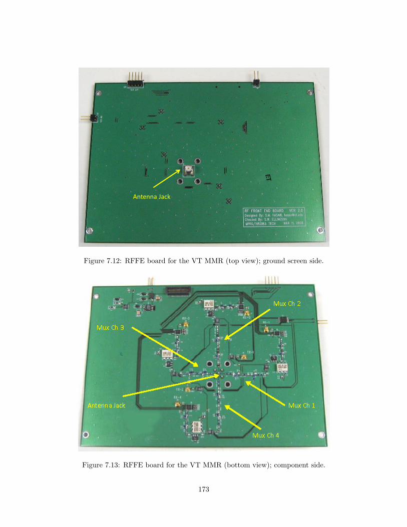
Antenna Jack
Figure 7.12: RFFE board for the VT MMR (top view); ground screen side.
Figure 7.13: RFFE board for the VT MMR (bottom view); component side.
173

Multiplexer
SW1
SW2
SW3
SW4
SW5
SW6
TX-1
TX-1
RX-1
RX-2
RX-3
RX-4
RFIC
Board
O/P
RF Front End Board
Figure 7.14: Block diagram of the RFFE board.
including the schematic, PCB layout, and bill of materials.
Since the receivers in the RFIC require differential signals, transformers have been used as baluns
to convert single-ended signals to/from RFFE to differential signals. Ports Rx-1 to Rx-4 use the
ETC1-1-13 1:1 transformer (frequency range 4.5 to 3000 MHz) from M/A-COM 2. Similar to
the receiver section, the RFIC also provides the transmitter output in differential form, which is
converted into single-ended using a transformer. Since the impedance for the RFIC transmitter
ports is 200Ω, we use a 1:4 transformer, Model ETC4-1T-7 (frequency range 6 to 1000 MHz) from
M/A-COM.
Like the performance of the evaluation board, at 800 MHz the measured gain of the receiver section
of this RFIC board is also 50 dB, input 1dB compression point is –26 dBm, and the image rejection
is around 30 dB3. Note that the performance of this RFIC, specifically the image rejection, can
be improved significantly if we optimize the various programmable parameters as discussed in2http://www.macom.com3Although not specifically of interest in this study, we also looked at transmit. Transmitter output power at
800 MHz is 1.5 dBm, output 1 dB compression point is 1.6 dBm, and sideband rejection is 17 dB.
174

Figure 7.15: RFIC board for the VT MMR.
Section 7.3.3. The implemented RFIC board consumes 1.1W power (10V @ 110 mA) during
reception and consumes 1.7W (10V @ 170 mA) power during transmission.
7.5.3 ADC/DAC Board
Figure 7.16 shows the ADC/DAC board. A detailed description of this board including the circuit
diagram, PCB layout, and bill of materials is presented in Appendix G.
The differential I and Q signals from the RFIC board are digitized using the AD9248 A/D converter
from Analog Devices4. This is a dual 14-bit ADC sampling 4 MSPS (in our design) which consumes
about 65 mA at 3V. Similarly, the AD9761 dual 10-bit D/A converter is used to generate differential
analog I and Q signals. This is an interpolating DAC which samples at 4 MSPS and consumes
about 50 mA at 3V. A compelling feature of this part is the availability of internal interpolation4http://www.analog.com
175

Figure 7.16: ADC/DAC board for the VT MMR (frequency synthesizer on reverse side).
filters which lead to a significantly reduced requirement for anti-alias filtering. This board also
contains a frequency synthesizer to supply 1 GHz reference frequency to the RFIC board.
7.5.4 FPGA Board
To process digital baseband signals in the VT MMR, we used a Stratix II DSP development board,
which contains a Stratix II EP2S60F1020C4 FPGA, from Altera5. This board was selected based
on our familiarity with this board due to work in other projects, as well as the availability of
a suitable audio CODEC, Model TLV320AIC23PW, from Texas Instruments6. All digital signal
processing is performed in the Stratix II FPGA. This FPGA is overkill for this application; only5http://www.altera.com6http://www.ti.com
176
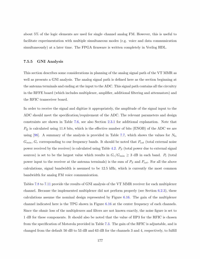
about 5% of the logic elements are used for single–channel analog FM. However, this is useful to
facilitate experimentation with multiple simultaneous modes (e.g. voice and data communication
simultaneously) at a later time. The FPGA firmware is written completely in Verilog HDL.
7.5.5 GNI Analysis
This section describes some considerations in planning of the analog signal path of the VT MMR as
well as presents a GNI analysis. The analog signal path is defined here as the section beginning at
the antenna terminals and ending at the input to the ADC. This signal path contains all the circuitry
in the RFFE board (which includes multiplexer, amplifier, additional filtering and attenuators) and
the RFIC transceiver board.
In order to receive the signal and digitize it appropriately, the amplitude of the signal input to the
ADC should meet the specification/requirement of the ADC. The relevant parameters and design
constraints are shown in Table 7.6, see also Section 2.3.1 for additional explanation. Note that
PQ is calculated using 11.8 bits, which is the effective number of bits (ENOB) of the ADC we are
using [98]. A summary of the analysis is provided in Table 7.7, which shows the values for Nb,
Gmin, Gr corresponding to our frequency bands. It should be noted that Pext (total external noise
power received by the receiver) is calculated using Table 4.2. PS (total power due to external signal
sources) is set to be the largest value which results in Gr/Gmin ≥ 3 dB in each band. Pt (total
power input to the receiver at the antenna terminals) is the sum of PS and Pext. For all the above
calculations, signal bandwidth is assumed to be 12.5 kHz, which is currently the most common
bandwidth for analog FM voice communication.
Tables 7.8 to 7.11 provide the results of GNI analysis of the VT MMR receiver for each multiplexer
channel. Because the implemented multiplexer did not perform properly (see Section 6.2.3), these
calculations assume the nominal design represented by Figure 6.16. The gain of the multiplexer
channel indicated here is the TPG shown in Figure 6.16 at the center frequency of each channels.
Since the ohmic loss of the multiplexers and filters are not known exactly, the noise figure is set to
1 dB for these components. It should also be noted that the value of IIP3 for the RFIC is chosen
from the specification of Motorola provided in Table 7.3. The gain of the RFIC is adjustable, and is
changed from the default 50 dB to 53 dB and 63 dB for the channels 3 and 4, respectively, to fulfill
177
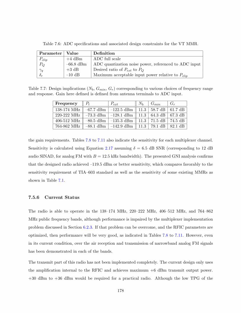
Table 7.6: ADC specifications and associated design constraints for the VT MMR.
Parameter Value DefinitionPclip +4 dBm ADC full scalePQ –66.8 dBm ADC quantization noise power, referenced to ADC inputγq +3 dB Desired ratio of Pext to PQ
δr –10 dB Maximum acceptable input power relative to Pclip
Table 7.7: Design implications (Nb, Gmin, Gr) corresponding to various choices of frequency rangeand response. Gain here defined is defined from antenna terminals to ADC input.
Frequency Pt Pext Nb Gmin Gr
138-174 MHz –67.7 dBm –122.5 dBm 11.3 58.7 dB 61.7 dB220-222 MHz –73.3 dBm –128.1 dBm 11.3 64.3 dB 67.3 dB406-512 MHz –80.5 dBm –135.3 dBm 11.3 71.5 dB 74.5 dB764-862 MHz –88.1 dBm –142.9 dBm 11.3 79.1 dB 82.1 dB
the gain requirements. Tables 7.8 to 7.11 also indicate the sensitivity for each multiplexer channel.
Sensitivity is calculated using Equation 2.17 assuming δ = 6.5 dB SNR (corresponding to 12 dB
audio SINAD, for analog FM with B = 12.5 kHz bandwidth). The presented GNI analysis confirms
that the designed radio achieved –119.5 dBm or better sensitivity, which compares favorably to the
sensitivity requirement of TIA–603 standard as well as the sensitivity of some existing MMRs as
shown in Table 7.1.
7.5.6 Current Status
The radio is able to operate in the 138–174 MHz, 220–222 MHz, 406–512 MHz, and 764–862
MHz public frequency bands, although performance is impaired by the multiplexer implementation
problem discussed in Section 6.2.3. If that problem can be overcome, and the RFIC parameters are
optimized, then performance will be very good, as indicated in Tables 7.8 to 7.11. However, even
in its current condition, over the air reception and transmission of narrowband analog FM signals
has been demonstrated in each of the bands.
The transmit part of this radio has not been implemented completely. The current design only uses
the amplification internal to the RFIC and achieves maximum +6 dBm transmit output power.
+30 dBm to +36 dBm would be required for a practical radio. Although the low TPG of the
178
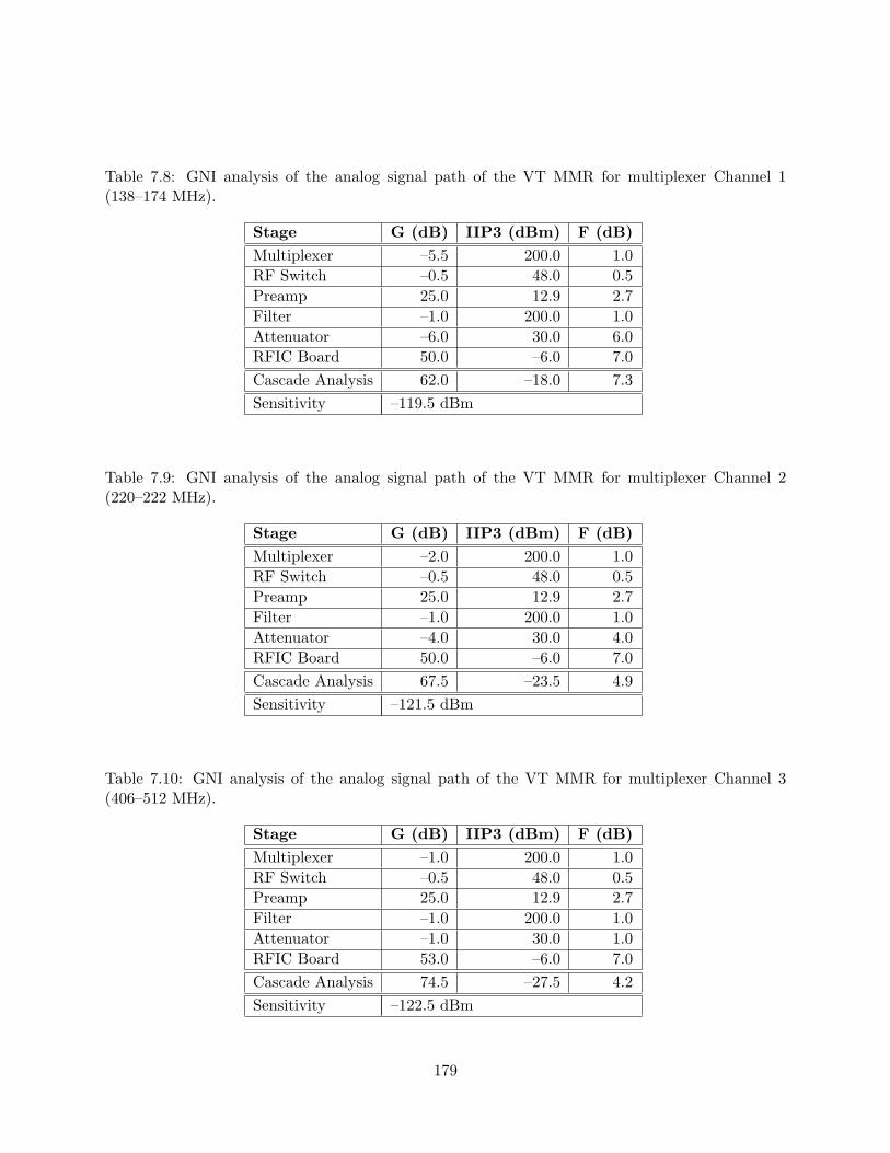
Table 7.8: GNI analysis of the analog signal path of the VT MMR for multiplexer Channel 1(138–174 MHz).
Stage G (dB) IIP3 (dBm) F (dB)Multiplexer –5.5 200.0 1.0RF Switch –0.5 48.0 0.5Preamp 25.0 12.9 2.7Filter –1.0 200.0 1.0Attenuator –6.0 30.0 6.0RFIC Board 50.0 –6.0 7.0Cascade Analysis 62.0 –18.0 7.3Sensitivity –119.5 dBm
Table 7.9: GNI analysis of the analog signal path of the VT MMR for multiplexer Channel 2(220–222 MHz).
Stage G (dB) IIP3 (dBm) F (dB)Multiplexer –2.0 200.0 1.0RF Switch –0.5 48.0 0.5Preamp 25.0 12.9 2.7Filter –1.0 200.0 1.0Attenuator –4.0 30.0 4.0RFIC Board 50.0 –6.0 7.0Cascade Analysis 67.5 –23.5 4.9Sensitivity –121.5 dBm
Table 7.10: GNI analysis of the analog signal path of the VT MMR for multiplexer Channel 3(406–512 MHz).
Stage G (dB) IIP3 (dBm) F (dB)Multiplexer –1.0 200.0 1.0RF Switch –0.5 48.0 0.5Preamp 25.0 12.9 2.7Filter –1.0 200.0 1.0Attenuator –1.0 30.0 1.0RFIC Board 53.0 –6.0 7.0Cascade Analysis 74.5 –27.5 4.2Sensitivity –122.5 dBm
179

Table 7.11: GNI analysis of the analog signal path of the VT MMR for multiplexer Channel 4(764–862 MHz).
Stage G (dB) IIP3 (dBm) F (dB)Multiplexer –3.5 200.0 1.0RF Switch –0.5 48.0 0.5Preamp 25.0 12.9 2.7Filter –1.0 200.0 1.0Attenuator –1.0 30.0 1.0RFIC Board 63.0 –6.0 7.0Cascade Analysis 82.0 –25.0 5.7Sensitivity –120.5 dBm
multiplexer is not problem for receiver, this would be a problem for transmit since good matching
(to achieve maximum power transfer) is required in order to mitigate the reflection of transmitted
power back into the transmit and receive sections of the radio. We did not address this issue in
the present work. For that reason, there is a need to modify the current design to increase the
transmission efficiency; perhaps by connecting the transmitter to the antenna through a separate
set of (variable) matching circuits. However, this left is left for future work.
Table 7.12 shows the power consumption of the VT MMR. The radio consumes approximately
1.51A current at 16V. We use a 4 A·h battery, which lasts for about 1.5 hours at this current draw.
As shown in the table, the FPGA board and user interface circuitry consume approximately 88%
of the total power. However, no attempt has been made to optimize the power consumption, and
in a practical implementation, these could easily be made dramatically less.
7.6 Summary
This chapter presented a description of a prototype multiband multimode radio based on direct
conversion architecture for public safety application. This prototype was designed to operate in all
the public safety frequency bands from 100 MHz to 1 GHz using just a single narrowband monopole
antenna, the size and shape of which is similar to those used by traditional mobile radios. The
multiplexer described in Section 6.2 is used to integrate the antenna with the receiver. This radio
advances the state–of–the–art in MMR by allowing a single traditional antenna to cover all bands
180

Table 7.12: Power consumption of the VT MMR prototype.
Board Power Current DrainRFFE 0.18 W 16V @ 10 mARFIC 1.70 W 16V @ 110 mAADC/DAC 0.99 W 16V @ 60 mAFPGA 13.28 W 16V @ 830 mAUser Interface &Others
8.00 W 16V @ 500 mA
Total 24.16 W 16V @ 1.51 A
over a very large tuning range to be received with sensitivity which is comparable to existing radios
which require antenna changes to accomplish the same goal. Table 7.1 shows this comparison.
Limitations of this radio are also discussed in Section 7.5.6.
181

Chapter 8
Conclusions
This dissertation described new concepts to design RF front ends focusing on the development
and evaluation of sensitivity–constrained RF multiplexers which allow the integration of a single
antenna to a receiver with large, multiband tuning ranges. Chapter 4 (“Sensitivity-Constrained
Front-End Design”) describes the concept of sensitivity–constrained design, develops the associated
theory and analysis, and provides a demonstration in field conditions. In Chapter 5 (“Multiplexer
Design”), this concept was extended to the design of multiplexers and once again verified through
field measurements. In Chapter 6 (“Multiplexer Application to a Multiband Multimode Radio”)
this approach was used to design a multiplexer for a public safety MMR with a small monopole
antenna. In Chapter 7 (“Design & Development of a Multiband Multimode Radio), we described
a complete multiband multimode radio using the multiplexer of Chapter 6.
In this chapter, principal findings and topics for future research are suggested.
8.1 Findings
The principal findings in this dissertation are as follows:
1. Sections 4.2 and 4.3 describe an “optimum” noise figure specification for wideband receivers,
which accounts for the trade–off between antenna–receiver match efficiency and bandwidth,
182
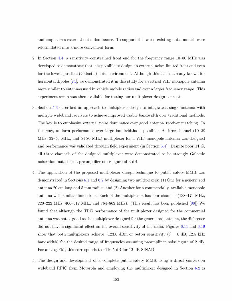
and emphasizes external noise dominance. To support this work, existing noise models were
reformulated into a more convenient form.
2. In Section 4.4, a sensitivity–constrained front end for the frequency range 10–80 MHz was
developed to demonstrate that it is possible to design an external noise–limited front end even
for the lowest possible (Galactic) noise environment. Although this fact is already known for
horizontal dipoles [74], we demonstrated it in this study for a vertical VHF monopole antenna
more similar to antennas used in vehicle mobile radios and over a larger frequency range. This
experiment setup was then available for testing our multiplexer design concept.
3. Section 5.3 described an approach to multiplexer design to integrate a single antenna with
multiple wideband receivers to achieve improved usable bandwidth over traditional methods.
The key is to emphasize external noise dominance over good antenna–receiver matching. In
this way, uniform performance over large bandwidths is possible. A three channel (10–28
MHz, 32–50 MHz, and 54-80 MHz) multiplexer for a VHF monopole antenna was designed
and performance was validated through field experiment (in Section 5.4). Despite poor TPG,
all three channels of the designed multiplexer were demonstrated to be strongly Galactic
noise–dominated for a preamplifier noise figure of 3 dB.
4. The application of the proposed multiplexer design technique to public safety MMR was
demonstrated in Sections 6.1 and 6.2 by designing two multiplexers: (1) One for a generic rod
antenna 20 cm long and 5 mm radius, and (2) Another for a commercially–available monopole
antenna with similar dimensions. Each of the multiplexers has four channels (138–174 MHz,
220–222 MHz, 406–512 MHz, and 764–862 MHz). (This result has been published [88]) We
found that although the TPG performance of the multiplexer designed for the commercial
antenna was not as good as the multiplexer designed for the generic rod antenna, the difference
did not have a significant effect on the overall sensitivity of the radio. Figures 6.11 and 6.19
show that both multiplexers achieve –123.0 dBm or better sensitivity (δ = 0 dB, 12.5 kHz
bandwidth) for the desired range of frequencies assuming preamplifier noise figure of 2 dB.
For analog FM, this corresponds to –116.5 dB for 12 dB SINAD.
5. The design and development of a complete public safety MMR using a direct conversion
wideband RFIC from Motorola and employing the multiplexer designed in Section 6.2 is
183
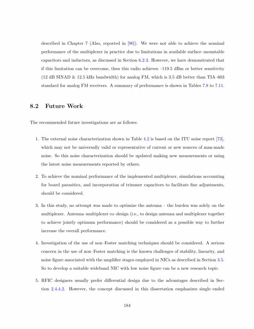
described in Chapter 7 (Also, reported in [90]). We were not able to achieve the nominal
performance of the multiplexer in practice due to limitations in available surface–mountable
capacitors and inductors, as discussed in Section 6.2.3. However, we have demonstrated that
if this limitation can be overcome, then this radio achieves –119.5 dBm or better sensitivity
(12 dB SINAD & 12.5 kHz bandwidth) for analog FM, which is 3.5 dB better than TIA–603
standard for analog FM receivers. A summary of performance is shown in Tables 7.8 to 7.11.
8.2 Future Work
The recommended future investigations are as follows:
1. The external noise characterization shown in Table 4.2 is based on the ITU noise report [73],
which may not be universally valid or representative of current or new sources of man-made
noise. So this noise characterization should be updated making new measurements or using
the latest noise measurements reported by others.
2. To achieve the nominal performance of the implemented multiplexer, simulations accounting
for board parasitics, and incorporation of trimmer capacitors to facilitate fine adjustments,
should be considered.
3. In this study, no attempt was made to optimize the antenna – the burden was solely on the
multiplexer. Antenna–multiplexer co–design (i.e., to design antenna and multiplexer together
to achieve jointly optimum performance) should be considered as a possible way to further
increase the overall performance.
4. Investigation of the use of non–Foster matching techniques should be considered. A serious
concern in the use of non–Foster matching is the known challenges of stability, linearity, and
noise figure associated with the amplifier stages employed in NICs as described in Section 3.5.
So to develop a suitable wideband NIC with low noise figure can be a new research topic.
5. RFIC designers usually prefer differential design due to the advantages described in Sec-
tion 2.4.4.2. However, the concept discussed in this dissertation emphasizes single–ended
184

circuitry. In order to make the proposed work more useful for practical implementation (e.g.,
eliminating the need for balun transformers) differential implementation of this work should
be considered.
6. Since this dissertation is mainly focused on the receiver, the transmitter part of the VT
MMR is not designed to achieve acceptable transmission efficiency. Future research is needed
to complete the integration of a single antenna to both of the transmitter and the receiver to
achieve good transmission efficiency as well as acceptable receive sensitivity.
185
Appendix A
Relationship Between Predetection
SNR and SINAD
The purpose of this appendix is to explain the relationship between the predetection signal–to–
noise ratio (SNR) and the audio signal–to–noise–and–distortion ratio (SINAD) for an analog FM
demodulation1. SINAD is defined as ratio of the signal including noise and distortion to the noise
and distortion component for an analog FM receiver.
In [99, pp. 169–172], Jakes gives the relationship between the audio signal power, S0, and the
signal power, S, as:
S0 =(1− e−ρ
)2S (A.1)
where ρ is the predetection SNR. The total audio noise, N , is given by:
N =a (1− e−ρ)2
ρ+
8πBWe−ρ√2(ρ + 2.35)
(A.2)
where B is the input signal bandwidth in Hz, W is the baseband lowpass cutoff frequency in Hz,
and a is B/(2W ).
We want to know S0/N as a function of ρ. A difficulty arises in doing this, because S0 is a function
of S, whereas N is not. Jakes deals with this by making the assumption that “the RMS frequency1This appendix based on notes provided by S.W. Ellingson, Virginia Tech, dated 1996.
186
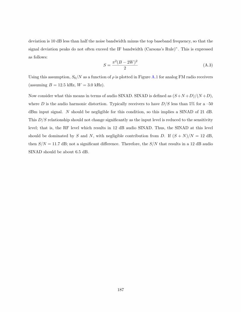
deviation is 10 dB less than half the noise bandwidth minus the top baseband frequency, so that the
signal deviation peaks do not often exceed the IF bandwidth (Carsons’s Rule)”. This is expressed
as follows:
S =π2(B − 2W )2
2(A.3)
Using this assumption, S0/N as a function of ρ is plotted in Figure A.1 for analog FM radio receivers
(assuming B = 12.5 kHz, W = 3.0 kHz).
Now consider what this means in terms of audio SINAD. SINAD is defined as (S+N +D)/(N +D),
where D is the audio harmonic distortion. Typically receivers to have D/S less than 5% for a –50
dBm input signal. N should be negligible for this condition, so this implies a SINAD of 21 dB.
This D/S relationship should not change significantly as the input level is reduced to the sensitivity
level; that is, the RF level which results in 12 dB audio SINAD. Thus, the SINAD at this level
should be dominated by S and N , with negligible contribution from D. If (S + N)/N = 12 dB,
then S/N = 11.7 dB; not a significant difference. Therefore, the S/N that results in a 12 dB audio
SINAD should be about 6.5 dB.
187

0 1 2 3 4 5 6 7 8 9 10-10
-5
0
5
10
15
20
25
30
35
40
SNR [dB]
Audio
SN
R [dB
]
Figure A.1: Audio SNR as a function of predetection SNR for analog FM (B = 12.5 kHz).
188
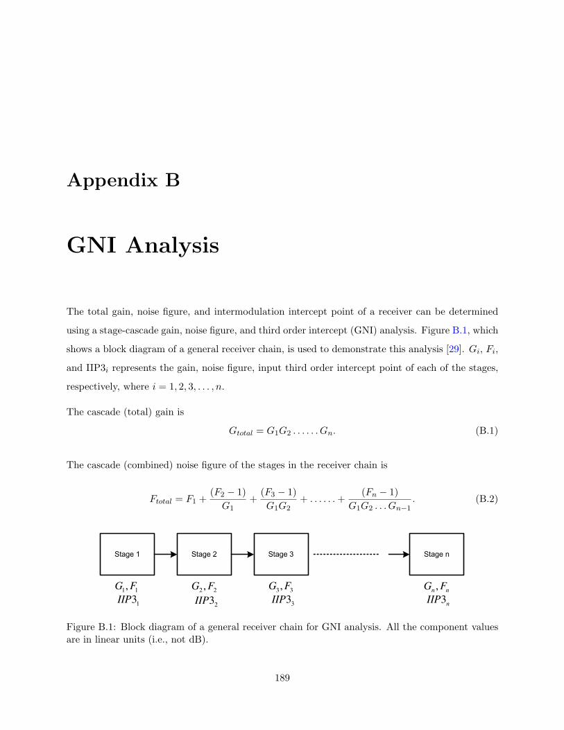
Appendix B
GNI Analysis
The total gain, noise figure, and intermodulation intercept point of a receiver can be determined
using a stage-cascade gain, noise figure, and third order intercept (GNI) analysis. Figure B.1, which
shows a block diagram of a general receiver chain, is used to demonstrate this analysis [29]. Gi, Fi,
and IIP3i represents the gain, noise figure, input third order intercept point of each of the stages,
respectively, where i = 1, 2, 3, . . . , n.
The cascade (total) gain is
Gtotal = G1G2 . . . . . . Gn. (B.1)
The cascade (combined) noise figure of the stages in the receiver chain is
Ftotal = F1 +(F2 − 1)
G1+
(F3 − 1)G1G2
+ . . . . . . +(Fn − 1)
G1G2 . . . Gn−1. (B.2)
Stage 1 Stage 2 Stage 3 Stage n
1 1,G F
13IIP
2 2,G F
3 3,G F ,n nG F
23IIP 3
3IIP 3n
IIP
Figure B.1: Block diagram of a general receiver chain for GNI analysis. All the component valuesare in linear units (i.e., not dB).
189

The cascade IIP3 is given by
1IIP3total
=1
IIP31+
G1
IIP32+
G1G2
IIP33+ . . . . . . +
G1G2 . . . Gn
IIP3n. (B.3)
The output third order intercept point (OIP3) is sometimes of interest. The relationship to IIP3
is simply OIP3 = G · (IIP3).
190

Appendix C
VHF Multiplexer Board
This appendix presents details of the design of the multiplexer board for the VHF monopole antenna
discussed in Section 5.4 (“VHF Monopole Multiplexer Design Example”). Figure C.1 shows the
schematic of the multiplexer board. The PCB layout of the implemented multiplexer board is
presented in Figure C.2. The bill of materials for this board is shown at the end of this appendix.
191

Fig
ure
C.1
:Sc
hem
atic
ofth
em
ulti
plex
erde
sign
edfo
rth
eV
HF
mon
opol
ean
tenn
a.
192

Fig
ure
C.2
:Top
laye
rof
the
mul
tipl
exer
boar
dde
sign
edfo
rth
eV
HF
mon
opol
ean
tenn
a.
193
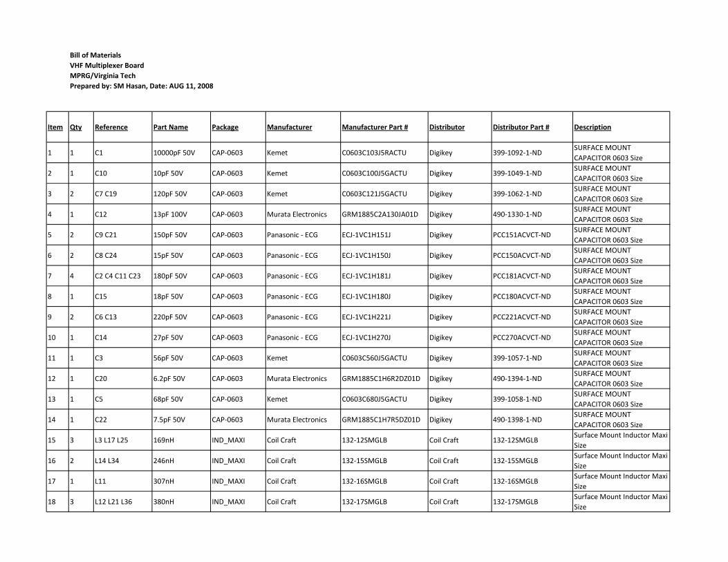
Bill of Materials
VHF Multiplexer Board
MPRG/Virginia Tech
Prepared by: SM Hasan, Date: AUG 11, 2008
Item Qty Reference Part Name Package Manufacturer Manufacturer Part # Distributor Distributor Part # Description
1 1 C1 10000pF 50V CAP-0603 Kemet C0603C103J5RACTU Digikey 399-1092-1-NDSURFACE MOUNT
CAPACITOR 0603 Size
2 1 C10 10pF 50V CAP-0603 Kemet C0603C100J5GACTU Digikey 399-1049-1-NDSURFACE MOUNT
CAPACITOR 0603 Size
3 2 C7 C19 120pF 50V CAP-0603 Kemet C0603C121J5GACTU Digikey 399-1062-1-NDSURFACE MOUNT
CAPACITOR 0603 Size
4 1 C12 13pF 100V CAP-0603 Murata Electronics GRM1885C2A130JA01D Digikey 490-1330-1-NDSURFACE MOUNT
CAPACITOR 0603 Size
5 2 C9 C21 150pF 50V CAP-0603 Panasonic - ECG ECJ-1VC1H151J Digikey PCC151ACVCT-NDSURFACE MOUNT
CAPACITOR 0603 Size
6 2 C8 C24 15pF 50V CAP-0603 Panasonic - ECG ECJ-1VC1H150J Digikey PCC150ACVCT-NDSURFACE MOUNT
CAPACITOR 0603 SizeCAPACITOR 0603 Size
7 4 C2 C4 C11 C23 180pF 50V CAP-0603 Panasonic - ECG ECJ-1VC1H181J Digikey PCC181ACVCT-NDSURFACE MOUNT
CAPACITOR 0603 Size
8 1 C15 18pF 50V CAP-0603 Panasonic - ECG ECJ-1VC1H180J Digikey PCC180ACVCT-NDSURFACE MOUNT
CAPACITOR 0603 Size
9 2 C6 C13 220pF 50V CAP-0603 Panasonic - ECG ECJ-1VC1H221J Digikey PCC221ACVCT-NDSURFACE MOUNT
CAPACITOR 0603 Size
10 1 C14 27pF 50V CAP-0603 Panasonic - ECG ECJ-1VC1H270J Digikey PCC270ACVCT-NDSURFACE MOUNT
CAPACITOR 0603 Size
11 1 C3 56pF 50V CAP-0603 Kemet C0603C560J5GACTU Digikey 399-1057-1-NDSURFACE MOUNT
CAPACITOR 0603 Size
12 1 C20 6.2pF 50V CAP-0603 Murata Electronics GRM1885C1H6R2DZ01D Digikey 490-1394-1-NDSURFACE MOUNT
CAPACITOR 0603 Size
13 1 C5 68pF 50V CAP-0603 Kemet C0603C680J5GACTU Digikey 399-1058-1-NDSURFACE MOUNT
CAPACITOR 0603 Size
14 1 C22 7.5pF 50V CAP-0603 Murata Electronics GRM1885C1H7R5DZ01D Digikey 490-1398-1-NDSURFACE MOUNT
CAPACITOR 0603 Size
15 3 L3 L17 L25 169nH IND_MAXI Coil Craft 132-12SMGLB Coil Craft 132-12SMGLBSurface Mount Inductor Maxi
Size
16 2 L14 L34 246nH IND_MAXI Coil Craft 132-15SMGLB Coil Craft 132-15SMGLBSurface Mount Inductor Maxi
Size
17 1 L11 307nH IND_MAXI Coil Craft 132-16SMGLB Coil Craft 132-16SMGLBSurface Mount Inductor Maxi
Size
18 3 L12 L21 L36 380nH IND_MAXI Coil Craft 132-17SMGLB Coil Craft 132-17SMGLBSurface Mount Inductor Maxi
Size
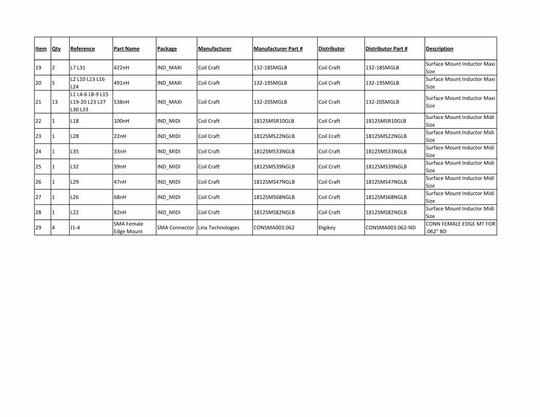
Item Qty Reference Part Name Package Manufacturer Manufacturer Part # Distributor Distributor Part # Description
19 2 L7 L31 422nH IND_MAXI Coil Craft 132-18SMGLB Coil Craft 132-18SMGLBSurface Mount Inductor Maxi
Size
20 5L2 L10 L13 L16
L24491nH IND_MAXI Coil Craft 132-19SMGLB Coil Craft 132-19SMGLB
Surface Mount Inductor Maxi
Size
21 13
L1 L4-6 L8-9 L15
L19-20 L23 L27
L30 L33
538nH IND_MAXI Coil Craft 132-20SMGLB Coil Craft 132-20SMGLBSurface Mount Inductor Maxi
Size
22 1 L18 100nH IND_MIDI Coil Craft 1812SMSR10GLB Coil Craft 1812SMSR10GLBSurface Mount Inductor Midi
Size
23 1 L28 22nH IND_MIDI Coil Craft 1812SMS22NGLB Coil Craft 1812SMS22NGLBSurface Mount Inductor Midi
Size
24 1 L35 33nH IND_MIDI Coil Craft 1812SMS33NGLB Coil Craft 1812SMS33NGLBSurface Mount Inductor Midi
Size
25 1 L32 39nH IND_MIDI Coil Craft 1812SMS39NGLB Coil Craft 1812SMS39NGLBSurface Mount Inductor Midi
Size
26 1 L29 47nH IND_MIDI Coil Craft 1812SMS47NGLB Coil Craft 1812SMS47NGLBSurface Mount Inductor Midi
Size
27 1 L26 68nH IND_MIDI Coil Craft 1812SMS68NGLB Coil Craft 1812SMS68NGLBSurface Mount Inductor Midi
27 1 L26 68nH IND_MIDI Coil Craft 1812SMS68NGLB Coil Craft 1812SMS68NGLBSurface Mount Inductor Midi
Size
28 1 L22 82nH IND_MIDI Coil Craft 1812SMS82NGLB Coil Craft 1812SMS82NGLBSurface Mount Inductor Midi
Size
29 4 J1-4SMA Female
Edge MountSMA Connector Linx Technologies CONSMA003.062 Digikey CONSMA003.062-ND
CONN FEMALE EDGE MT FOR
.062" BD
Appendix D
Superheterodyne Downconverter
This appendix documents the design of the superheterodyne RF downconverter board (RFDC) for
the VT MMR discussed in Section 7.2 (“Original Superhet Architecture”). Figures D.1 and D.2
show the schematic of the RFDC board. The PCB layout of the implemented RFDC board is
shown in Figure D.3. The bill of materials for this board is shown at the end of this appendix.
196

Fig
ure
D.1
:Sc
hem
atic
ofth
esu
perh
eter
odyn
eR
Fdo
wnc
onve
rter
boar
dde
sign
edfo
rth
ein
itia
lV
TM
MR
prot
otyp
e(c
onti
nues
inFig
ure
D.2
).
197
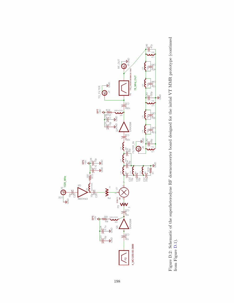
Fig
ure
D.2
:Sc
hem
atic
ofth
esu
perh
eter
odyn
eR
Fdo
wnc
onve
rter
boar
dde
sign
edfo
rth
ein
itia
lV
TM
MR
prot
otyp
e(c
onti
nued
from
Fig
ure
D.1
).
198

Fig
ure
D.3
:Top
laye
rof
the
supe
rhet
erod
yne
RF
dow
ncon
vert
erbo
ard
desi
gned
for
the
init
ialV
TM
MR
prot
otyp
e.
199

Bill of Materials
NIJ RF Downconverter Board, Version 1.0
MPRG/Virginia Tech
Prepared by: SM Hasan, Date: AUG 01, 2006
Item Qty Reference Part Name Package Manufacturer Mfg. No. Distributor Distributor No. Description
1 17
C2, C5, C7, C8, C10, C11,
C13, C14, C15, C21, C23,
C25, C26, C28, C29, C31,
C39
10p C0603 TDK Corporation C1608C0G1H100D Digikey 445-1269-1-ND CAP CER 10PF 50V C0G 0603
2 2 C1, C4 22p C0603 TDK Corporation C1608C0G1H102J Digikey 445-1293-1-ND CAP CER 1000PF 50V C0G 5% 0603
3 7C3, C6, C9, C12, C24, C27,
C30 0.1u C0603 TDK Corporation C1608Y5V1H104Z Digikey 445-1324-1-ND CAP CER .10UF 50V Y5V 0603
4 1 C16 1.0p C0603 AVX Corporation 06035J1R0BBTTR Digikey 478-2808-1-NDCAP CERAMIC 1.0PF 50V 0603
RFSMD
5 1 C17 3.0p C0603 AVX Corporation 06035J3R0BBTTR Digikey 478-2817-1-NDCAP CERAMIC 3.0PF 50V 0603
RFSMD
6 1 C40 3.9p C0603 AVX Corporation 06035J3R9BBTTR Digikey 478-2819-1-NDCAP CERAMIC 3.9PF 50V 0603
RFSMD
7 1 C18 2.2p C0603 AVX Corporation 06035J2R2BBTTR Digikey 478-2814-1-NDCAP CERAMIC 2.2PF 50V 0603
RFSMD
8 1 C19 0.8p C0603 AVX Corporation 06035J0R8PBTTR Digikey 478-2806-1-NDCAP CERAMIC .8PF 50V 0603 RF
SMD8 1 C19 0.8p C0603 AVX Corporation 06035J0R8PBTTR Digikey 478-2806-1-ND
SMD
9 1 C20 2.4p C0603 AVX Corporation 06035J2R4BBTTR Digikey 478-2815-1-NDCAP CERAMIC 2.4PF 50V 0603
RFSMD
10 2 C36, C44 12p C0603 AVX Corporation C1608C0G1H120J Digikey 445-1270-1-ND CAP CER 12PF 50V C0G 5% 0603
11 1 C33 15p C0603 TDK Corporation C1608C0G1H150J Digikey 445-1271-1-ND CAP CER 15PF 50V C0G 5% 0603
12 2 C35, C41 30p C0603 Murata Electronics GRM1885C1H300JA01D Digikey 490-1414-2-ND CAP CER 30PF 50V 5% C0G 0603
13 1 C37 33p C0603 TDK Corporation C1608C0G1H330J Digikey 445-1275-2-ND CAP CER 33PF 50V C0G 5% 0603
14 1 C34 39p C0603 TDK Corporation C1608C0G1H390J Digikey 445-1276-2-ND CAP CER 39PF 50V C0G 5% 0603
15 2 C45, C46 47p C0603 TDK Corporation C1608C0G1H470J Digikey 445-1277-2-ND CAP CER 47PF 50V C0G 5% 0603
16 1 C42 68p C0603 TDK Corporation C1608C0G1H680J Digikey 445-1279-2-ND CAP CER 68PF 50V C0G 5% 0603
17 2 C32, C38 100p C0603 TDK Corporation C1608C0G1H101J Digikey 445-1281-2-ND CAP CER 100PF 50V C0G 5% 0603
18 1 C43 120p C0603 TDK Corporation C1608C0G1H121J Digikey 445-1282-2-ND CAP CER 120PF 50V C0G 5% 0603
19 2 F1, F2LARK_MC1250-60-
3MMMC1250 Lark Engineering Inc LARK_MC1250-60-3MM Lark Engineering Inc LARK_MC1250-60-3MM LARK FILTER
20 1 F3TTE_K4938-
58/98M-20-1405TTE20 TTE Inc TTE_K4938-58/98M-20-1405 TTE Inc
TTE_K4938-58/98M-20-
1405TTE FILTER
21 6 J1, J2, J5, J6, J7, J8 MMCX MMCX Emerson 135-3711-201 Digikey J821-ND MMCX CONN

Item Qty Reference Part Name Package Manufacturer Mfg. No. Distributor Distributor No. Description
22 1 JP1 9V 1X02 Mill-Max Manufacturing 890-90-036-10-800000 Digikey 89090-03610800000-ND SQUARE HEAD
23 1 L6 2.2n 0402/0603 Coil Craft 0603CS-2N2X_LU Coil Craft 0603CS-2N2X_LU Inductor
24 2 L5, L7 2.7n 0402/0603 Coil Craft 0402CS-2N7X_LU Coil Craft 0402CS-2N7X_LU Inductor
25 2 L3, L4 6.8n 0402/0603 Coil Craft 0603CS-6N8X_LU Coil Craft 0603CS-6N8X_LU Inductor
26 1 L13 33n 0402/0603 Coil Craft 0603CS-33NX_LU Coil Craft 0603CS-33NX_LU Inductor
27 1 L21 36n 0402/0603 Coil Craft 0603CS-36NX_LU Coil Craft 0603CS-36NX_LU Inductor
28 2 L12, L14 39n 0402/0603 Coil Craft 0603CS-39NX_LU Coil Craft 0603CS-39NX_LU Inductor
29 2 L20 72n 0402/0603 Coil Craft 0603CS-72NX_LU Coil Craft 0603CS-72NX_LU Inductor
30 1 L24 82n 0402/0603 Coil Craft 0603CS-82NX_LU Coil Craft 0603CS-82NX_LU Inductor
31 1 L10 91n 0402/0603 Coil Craft 0603CS-91NX_LU Coil Craft 0603CS-91NX_LU Inductor
32 2 L11, L22 100n 0402/0603 Coil Craft 0603CS-R10X_LU Coil Craft 0603CS-R10X_LU Inductor32 2 L11, L22 100n 0402/0603 Coil Craft 0603CS-R10X_LU Coil Craft 0603CS-R10X_LU Inductor
33 1 L18 150n 0402/0603 Coil Craft 0603CS-R15X_LU Coil Craft 0603CS-R15X_LU Inductor
34 1 L23 330n 0402/0603 Coil Craft 0603CS-R33X_LU Coil Craft 0603CS-R33X_LU Inductor
35 1 L19 820n 0402/0603 JW Miller PM1008-R82K-RC Digikey M8475CT-ND INDUCTOR CHIP .82UH 10% SMD
36 2 M1, M2 SYM-11 TTT167 Mini Circuits SYM-11 Mini Circuits SYM-11 MIXER
37 4 P1, P2, P3, P4 3 AF320 Mini Circuits PAT-3 Mini Circuits PAT-3 PAT
38 1 Q2 ERA-6SM WW107 Mini Circuits ERA-6SM Mini Circuits ERA-6SM AMPLIFIER
39 6 Q1, Q3, Q4, Q5, Q6, Q7 ERA-3SM WW107 Mini Circuits ERA-3SM Mini Circuits ERA-3SM AMPLIFIER
40 1 R5 56 R2512 Panasonic - ECG ERJ-1WYJ560U Digikey P56XCT-ND RES 56 OHM 1W 5% 2512 SMD
41 6 R1, R6, R8, R9,R13, R14 160 R2512 Panasonic - ECG ERJ-1TYJ161U Digikey PT160XTR-ND RES 160 OHM 1W 5% 2512 SMD
42 2 R7, R15 51 R0603 Susumu Co Ltd RR0816Q-510-D Digikey RR08Q51DCT-ND RES 51 OHM 1/16W .5% 0603 SMD
43 7U$1, U$2, U$3, U$4, U$5,
U$6, U$7ADCH-80A CD542 Mini Circuits ADCH-80A Mini Circuits ADCH-80A RF CHOKE
Appendix E
RF Front End Board
This appendix documents the design of the RF front end (RFFE) board for the VT MMR discussed
in Section 7.5.1 (“RFFE Board”). Note that the design of the multiplexer implemented in this
board is already described in detail in Section 6.2 (“Multiplexer Design for a Real Antenna”). This
appendix documents the design of the rest of the board.
E.1 Board Overview
A block diagram of the RFFE board is shown in Figure 7.14. In this section, Figure E.1 and
Table E.1 show the input/output ports of the RFFE board.
A schematic of the multiplexer section including the RF switches, which control the receive/transmit
selection, is shown in Figure E.2. Table E.3 shows the receive/transmit switch control signals.
Figure E.3 show the schematic of the amplifier section. This figure also contains the circuit diagram
of four 5th order Chebyshev bandpass filters, which are connected at the output of the amplifiers,
to perform additional filtering. The frequency responses of these filters are shown in Figure E.5.
To control the gain of the received signal, we use a 5-bit digitally–controlled attenuator, Model
HMC470LP3 from Hittite Microwave Inc. Figure E.4 shows a schematic of the attenuator section.
Table E.2 shows how attenuator control signals are used to request various levels of attenuation.
202
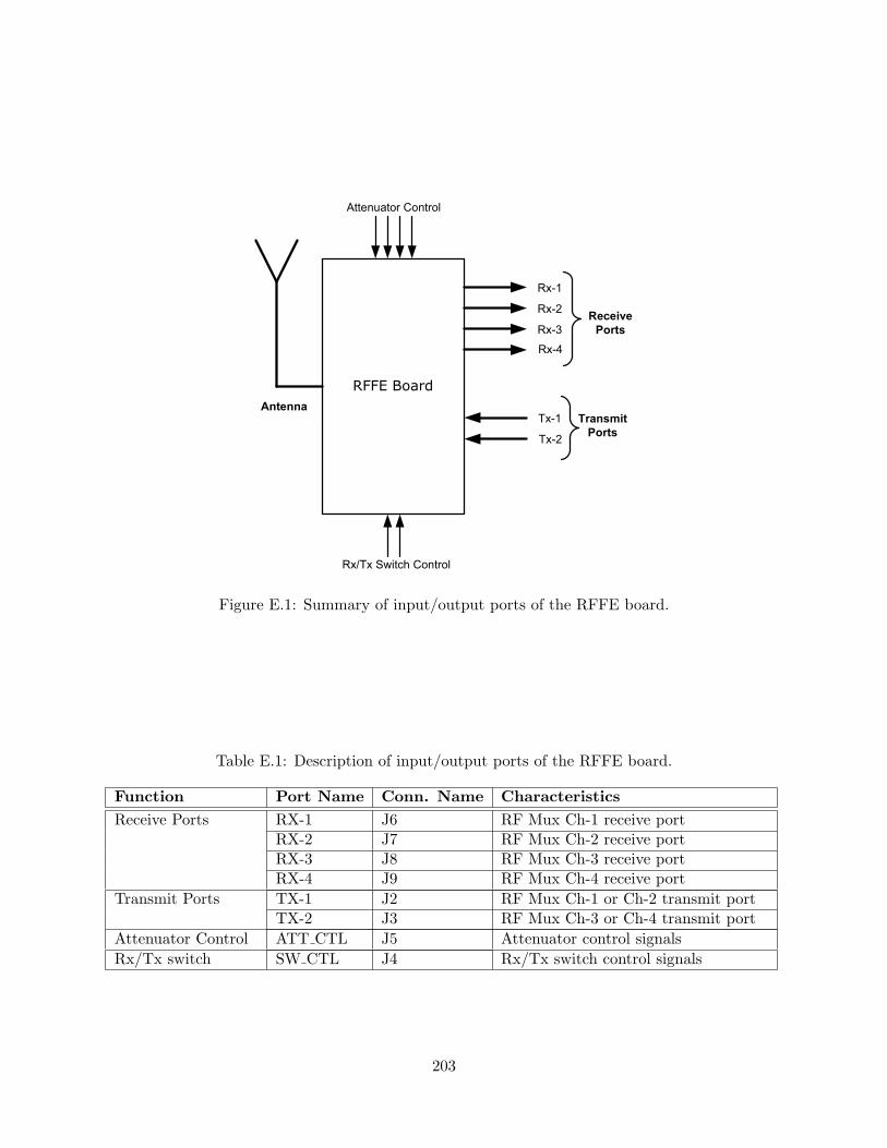
RFFE Board
Rx/Tx Board Overview
Rx-1
Receive
Ports
Transmit
Ports
Attenuator Control
Rx/Tx Switch Control
Rx-2
Rx-3
Rx-4
Tx-1
Tx-2
Antenna
Figure E.1: Summary of input/output ports of the RFFE board.
Table E.1: Description of input/output ports of the RFFE board.
Function Port Name Conn. Name CharacteristicsReceive Ports RX-1 J6 RF Mux Ch-1 receive port
RX-2 J7 RF Mux Ch-2 receive portRX-3 J8 RF Mux Ch-3 receive portRX-4 J9 RF Mux Ch-4 receive port
Transmit Ports TX-1 J2 RF Mux Ch-1 or Ch-2 transmit portTX-2 J3 RF Mux Ch-3 or Ch-4 transmit port
Attenuator Control ATT CTL J5 Attenuator control signalsRx/Tx switch SW CTL J4 Rx/Tx switch control signals
203

Fig
ure
E.2
:Sc
hem
atic
ofth
em
ulti
plex
eran
dsw
itch
sect
ion
ofth
eR
FFE
boar
d.
204

Fig
ure
E.3
:Sc
hem
atic
ofth
eam
plifi
erse
ctio
nof
the
RFFE
boar
d.
205

Fig
ure
E.4
:Sc
hem
atic
ofth
eat
tenu
ator
sect
ion
ofth
eR
FFE
boar
d.
206
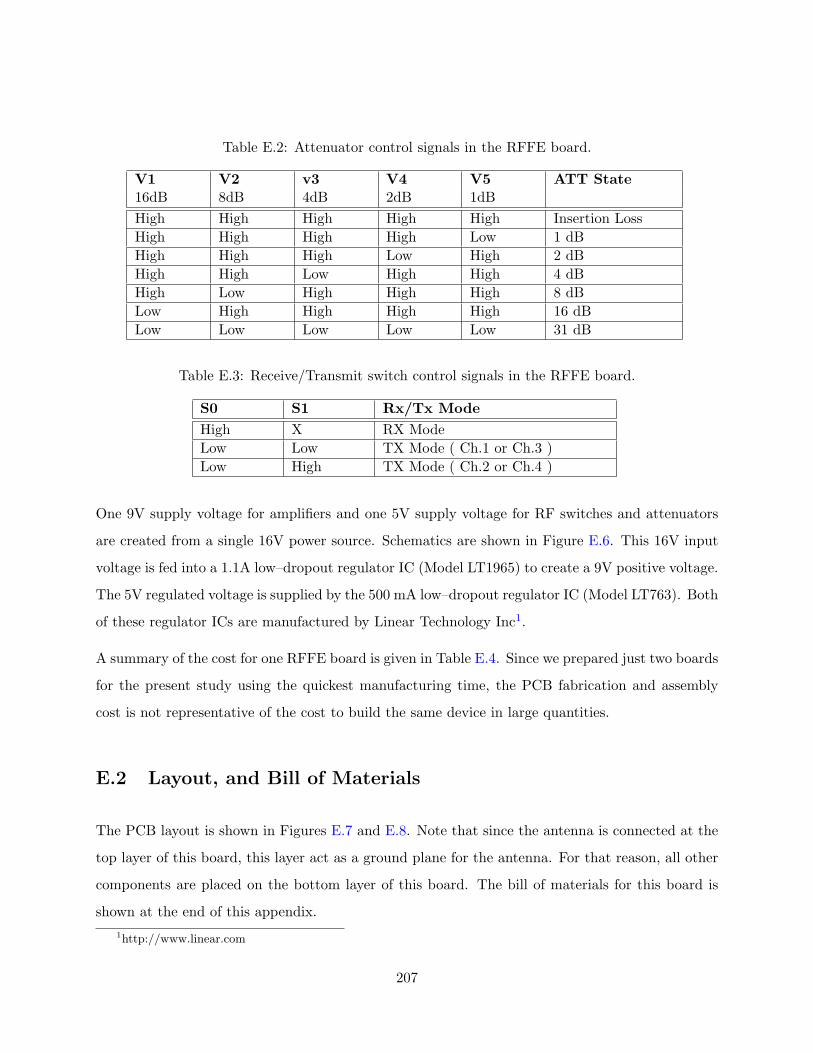
Table E.2: Attenuator control signals in the RFFE board.
V1 V2 v3 V4 V5 ATT State16dB 8dB 4dB 2dB 1dBHigh High High High High Insertion LossHigh High High High Low 1 dBHigh High High Low High 2 dBHigh High Low High High 4 dBHigh Low High High High 8 dBLow High High High High 16 dBLow Low Low Low Low 31 dB
Table E.3: Receive/Transmit switch control signals in the RFFE board.
S0 S1 Rx/Tx ModeHigh X RX ModeLow Low TX Mode ( Ch.1 or Ch.3 )Low High TX Mode ( Ch.2 or Ch.4 )
One 9V supply voltage for amplifiers and one 5V supply voltage for RF switches and attenuators
are created from a single 16V power source. Schematics are shown in Figure E.6. This 16V input
voltage is fed into a 1.1A low–dropout regulator IC (Model LT1965) to create a 9V positive voltage.
The 5V regulated voltage is supplied by the 500 mA low–dropout regulator IC (Model LT763). Both
of these regulator ICs are manufactured by Linear Technology Inc1.
A summary of the cost for one RFFE board is given in Table E.4. Since we prepared just two boards
for the present study using the quickest manufacturing time, the PCB fabrication and assembly
cost is not representative of the cost to build the same device in large quantities.
E.2 Layout, and Bill of Materials
The PCB layout is shown in Figures E.7 and E.8. Note that since the antenna is connected at the
top layer of this board, this layer act as a ground plane for the antenna. For that reason, all other
components are placed on the bottom layer of this board. The bill of materials for this board is
shown at the end of this appendix.1http://www.linear.com
207
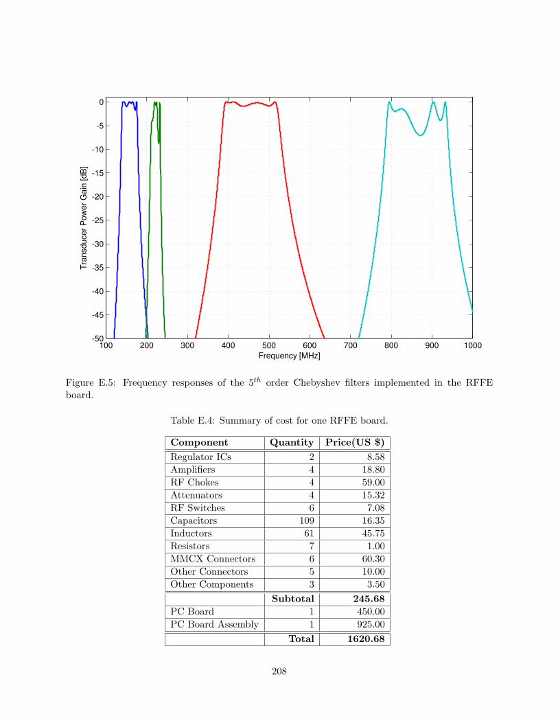
100 200 300 400 500 600 700 800 900 1000-50
-45
-40
-35
-30
-25
-20
-15
-10
-5
0
Frequency [MHz]
Tra
nsducer
Pow
er
Gain
[dB
]
Figure E.5: Frequency responses of the 5th order Chebyshev filters implemented in the RFFEboard.
Table E.4: Summary of cost for one RFFE board.
Component Quantity Price(US $)Regulator ICs 2 8.58Amplifiers 4 18.80RF Chokes 4 59.00Attenuators 4 15.32RF Switches 6 7.08Capacitors 109 16.35Inductors 61 45.75Resistors 7 1.00MMCX Connectors 6 60.30Other Connectors 5 10.00Other Components 3 3.50
Subtotal 245.68PC Board 1 450.00PC Board Assembly 1 925.00
Total 1620.68
208
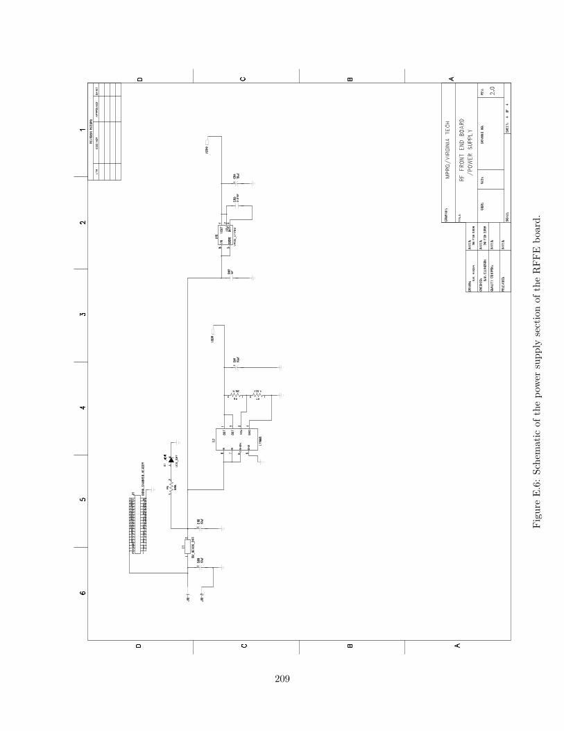
Fig
ure
E.6
:Sc
hem
atic
ofth
epo
wer
supp
lyse
ctio
nof
the
RFFE
boar
d.
209
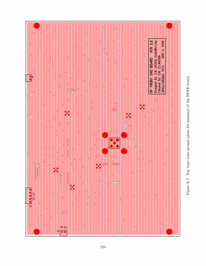
Fig
ure
E.7
:Top
laye
r(a
lso
grou
ndpl
ane
for
ante
nna)
ofth
eR
FFE
boar
d.
210

Fig
ure
E.8
:B
otto
mla
yer
(com
pone
ntsi
de)
ofth
eR
FFE
boar
d.
211

Bill of Materials
RFFE Board, Ver.2.0
MPRG/Virginia Tech
Prepared By: S.M. Hasan, Date: MAR 11, 2008
Item Qty Reference Part Name Package Manufacturer Manufacturer Part# Distributor Distributor Part# Description
1 1 U1 74VHCT04AMTC 14-TSSOP FAIRCHILD 74VHCT04AMTC Mouser 512-74VHCT04AMTC HEX INVERTER
2 4 L21 L27 L33 L39 ADCH-80A CD542 Minicircuits ADCH-80A+ Minicircuits ADCH-80A+ RF Choke
3 1 C93 0.01uF 100V CAP_1210 AVX Corporation 12101C103KAT2A Digikey 478-1608-1-ND
SURFACE MOUNT
CAPACITOR 0.098 X 0.126
INCHES
4 1 C92 1uF 100V CAP_1210 AVX Corporation 12101C105KAT2A Digikey 478-2570-1-ND
SURFACE MOUNT
CAPACITOR 0.098 X 0.126
INCHES
5 4 C24 C33 C42 C51 0.1uF 50V CAP_0603 Murata Electronics GRM188R71H104KA93D Digikey 490-1519-1-NDSURFACE MOUNT
CAPACITOR 0603 Size
6 3 C52 C54 C56 0.3pF 50V CAP_0603 AVX Corporation 06035J0R3PBTTR Digikey 478-2801-1-NDSURFACE MOUNT
CAPACITOR 0603 Size
7 1 C86 0.4pF 250V CAP_0603 AVX Corporation SQCSVA0R4BAT1A Digikey 478-3483-1-NDSURFACE MOUNT
CAPACITOR 0603 Size
8 3 C10 C36 C99 0.5pF 100V CAP_0603 Murata Electronics GQM1885C2AR50CB01D Digikey 490-3551-1-NDSURFACE MOUNT
CAPACITOR 0603 Size
9 1 C106 0.6pF 250V CAP_0603 AVX Corporation SQCSVA0R6BAT1A Digikey 478-3484-1-NDSURFACE MOUNT
CAPACITOR 0603 Size
10 4 C8 C13 C78 C107 0.7pF 50V CAP_0603 AVX Corporation 06035J0R7PBSTR Digikey 478-4445-1-NDSURFACE MOUNT
CAPACITOR 0603 Size
11 4 C16 C34 C38 C101 0.8pF 250V CAP_0603 AVX Corporation SQCSVA0R8BAT1A Digikey 478-3485-1-NDSURFACE MOUNT
CAPACITOR 0603 Size
12 3 C20 C105 C109 0.9pF 50V CAP_0603 AVX Corporation 06035J0R9PBTTR Digikey 478-2807-1-NDSURFACE MOUNT
CAPACITOR 0603 Size
13 2 C11 C15 1.1pF 250V CAP_0603 AVX Corporation SQCSVA1R1BAT1A Digikey 478-3487-1-NDSURFACE MOUNT
CAPACITOR 0603 Size
14 4 C43 C47 C97 C108 1.5pF 250V CAP_0603 AVX Corporation SQCSVA1R5BAT1A Digikey 478-3489-1-NDSURFACE MOUNT
CAPACITOR 0603 Size
15 1 C27 1.8pF 250V CAP_0603 AVX Corporation SQCSVA1R8BAT1A Digikey 478-3490-1-NDSURFACE MOUNT
CAPACITOR 0603 Size
16 14C63-64 C71-72 C79-80 C87-88
C96 C98 C100 C102-1041000pF 50V CAP_0603 AVX Corporation 06035C102KAT2A Digikey 478-1215-1-ND
SURFACE MOUNT
CAPACITOR 0603 Size
17 2 C2 C4 100pF 50V CAP_0603 AVX Corporation 06035A101KAT2A Digikey 478-3717-1-NDSURFACE MOUNT
CAPACITOR 0603 Size
18 12 C21-23 C30-32 C39-41 C48-50 10pF 250V CAP_0603 AVX Corporation SQCSVA100JAT1A Digikey 478-3502-1-NDSURFACE MOUNT
CAPACITOR 0603 Size
19 2 C26 C28 110pF 100V CAP_0603 Murata Electronics GRM1885C2A111JA01D Digikey 490-1352-1-NDSURFACE MOUNT
CAPACITOR 0603 Size
20 1 C70 18pF 250V CAP_0603 AVX Corporation SQCSVA180JAT1A Digikey 478-3505-1-NDSURFACE MOUNT
CAPACITOR 0603 Size
21 3 C6 C18 C45 1pF 250V CAP_0603 AVX Corporation SQCSVA1R0BAT1A Digikey 478-3486-1-NDSURFACE MOUNT
CAPACITOR 0603 Size

Item Qty Reference Part Name Package Manufacturer Manufacturer Part# Distributor Distributor Part# Description
22 1 C57 2.4pF 250V CAP_0603 AVX Corporation SQCSVA2R4BAT1A Digikey 478-3493-1-NDSURFACE MOUNT
CAPACITOR 0603 Size
23 2 C25 C29 2.7pF 250V CAP_0603 AVX Corporation SQCSVA2R7BAT1A Digikey 478-3494-1-NDSURFACE MOUNT
CAPACITOR 0603 Size
24 2 C35 C37 200pF 100V CAP_0603 Murata Electronics GRM1885C2A201JA01D Digikey 490-1358-1-NDSURFACE MOUNT
CAPACITOR 0603 Size
25 16 C58-61 C66-69 C74-77 C82-85 330pF 50V CAP_0603 Panasonic ECJ-1VC1H331J Digikey PCC331ACVCT-NDSURFACE MOUNT
CAPACITOR 0603 Size
26 5 C17 C19 C53 C55 C95 33pF 250V CAP_0603 AVX Corporation SQCSVA330JAT1A Digikey 478-3511-1-NDSURFACE MOUNT
CAPACITOR 0603 Size
27 2 C7 C9 360pF 100V CAP_0603 Murata Electronics GRM1885C2A361JA01D Digikey 490-1364-1-NDSURFACE MOUNT
CAPACITOR 0603 Size
28 6 C12 C14 C44 C46 C62 C81 39pF 250V CAP_0603 AVX Corporation SQCSVA390JAT1A Digikey 478-3512-1-NDSURFACE MOUNT
CAPACITOR 0603 Size
29 1 C1 3pF 250V CAP_0603 AVX Corporation SQCSVA3R0BAT1A Digikey 478-3495-1-NDSURFACE MOUNT
CAPACITOR 0603 Size
30 1 C65 4.7pF 250V CAP_0603 AVX Corporation SQCSVA4R7CAT1A Digikey 478-3498-1-NDSURFACE MOUNT
CAPACITOR 0603 Size
31 1 C3 5.1pF 100V CAP_0603 Murata Electronics GQM1885C2A5R1CB01D Digikey 490-3559-1-NDSURFACE MOUNT
CAPACITOR 0603 Size
32 1 C5 8.2pF 250V CAP_0603 AVX Corporation SQCSVA8R2CAT1A Digikey 478-3501-1-NDSURFACE MOUNT
CAPACITOR 0603 Size
33 1 C73 9.1pF 50V CAP_0603 Murata Electronics GQM1885C1H9R1CB01D Digikey 490-3569-1-NDSURFACE MOUNT
CAPACITOR 0603 Size
34 4 C89-91 C94 10uF 16V CAP_3216 Rohm TCA1C106M8R Digikey 511-1473-1-ND CAP TANTALUM
35 1 J11CONN_SAM8128_HEADE
RPlug Samtec Inc QTE-020-01-X-D-A Digikey SAM8128-ND
HIGH SPEED HEADER 40
PINS
36 1 J1 CONN_RPSMA-THROUGH SMA Linx Technologies CONREVSMA001 Digikey CONREVSMA001-NDSMA Through Hole
Connector
37 4 U2-5 GALI-74 DF782 Mincircuits GALI-74+ Minicircuits GALI-74+ Monolithic Amplifier
38 6 S1-6 HMC284MS8G MS8G HITTITE HMC284MS8G HITTITE HMC284MS8G RF SWITHC
39 4 U6-9 HMC470LP3 LP3 HITTITE HMC470LP3 HITTITE HMC470LP3 5 BIT DIGITAL ATTENUATOR
40 1 D1 LED_SMT SMT LITE-ON LTST-C190GKT Digikey 160-1183-1-ND LIGHT EMITTING DIODE
41 1 E2 LT1965 MSOP8G LINEAR TECHNOLOGY LT1965 Digikey LT1965IMS8E#PBF-ND LINEAR LDO REGULATOR
42 4 L17 L19 L41 L43 1.6nH L_0603 Coilcraft 0603CS-1N6X_LU Coilcraft 0603CS-1N6X_LUSurface Mount Inductor
0603 Size
43 1 L30 1000nH L_0603 Coilcraft 0603LS-102X_LB Coilcraft 0603LS-102X_LBSurface Mount Inductor
0603 Size
44 4 L15-16 L20 L56 100nH L_0603 Coilcraft 0603CS-R10X_LU Coilcraft 0603CS-R10X_LUSurface Mount Inductor
0603 Size
45 1 L58 10nH L_0603 Coilcraft 0603CS-10NX_LU Coilcraft 0603CS-10NX_LUSurface Mount Inductor
0603 Size
46 1 L18 110nH L_0603 Coilcraft 0603CS-R11X_LU Coilcraft 0603CS-R11X_LUSurface Mount Inductor
0603 Size
47 2 L8 L10 1200nH L_0603 Coilcraft 0603LS-122X_LB Coilcraft 0603LS-122X_LBSurface Mount Inductor
0603 Size
48 5 L11 L36 L40 L42 L44 120nH L_0603 Coilcraft 0603CS-R12X_LU Coilcraft 0603CS-R12X_LUSurface Mount Inductor
0603 Size
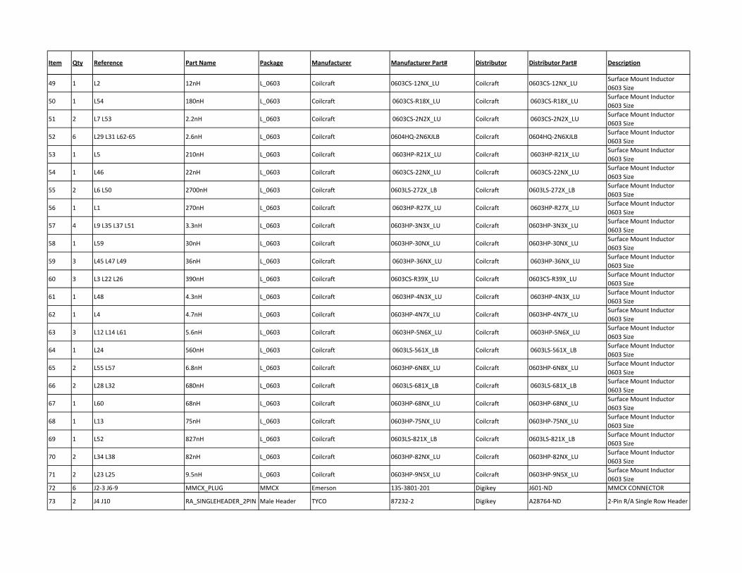
Item Qty Reference Part Name Package Manufacturer Manufacturer Part# Distributor Distributor Part# Description
49 1 L2 12nH L_0603 Coilcraft 0603CS-12NX_LU Coilcraft 0603CS-12NX_LUSurface Mount Inductor
0603 Size
50 1 L54 180nH L_0603 Coilcraft 0603CS-R18X_LU Coilcraft 0603CS-R18X_LUSurface Mount Inductor
0603 Size
51 2 L7 L53 2.2nH L_0603 Coilcraft 0603CS-2N2X_LU Coilcraft 0603CS-2N2X_LUSurface Mount Inductor
0603 Size
52 6 L29 L31 L62-65 2.6nH L_0603 Coilcraft 0604HQ-2N6XJLB Coilcraft 0604HQ-2N6XJLBSurface Mount Inductor
0603 Size
53 1 L5 210nH L_0603 Coilcraft 0603HP-R21X_LU Coilcraft 0603HP-R21X_LUSurface Mount Inductor
0603 Size
54 1 L46 22nH L_0603 Coilcraft 0603CS-22NX_LU Coilcraft 0603CS-22NX_LUSurface Mount Inductor
0603 Size
55 2 L6 L50 2700nH L_0603 Coilcraft 0603LS-272X_LB Coilcraft 0603LS-272X_LBSurface Mount Inductor
0603 Size
56 1 L1 270nH L_0603 Coilcraft 0603HP-R27X_LU Coilcraft 0603HP-R27X_LUSurface Mount Inductor
0603 Size
57 4 L9 L35 L37 L51 3.3nH L_0603 Coilcraft 0603HP-3N3X_LU Coilcraft 0603HP-3N3X_LUSurface Mount Inductor
0603 Size
58 1 L59 30nH L_0603 Coilcraft 0603HP-30NX_LU Coilcraft 0603HP-30NX_LUSurface Mount Inductor
0603 Size
59 3 L45 L47 L49 36nH L_0603 Coilcraft 0603HP-36NX_LU Coilcraft 0603HP-36NX_LUSurface Mount Inductor
0603 Size
60 3 L3 L22 L26 390nH L_0603 Coilcraft 0603CS-R39X_LU Coilcraft 0603CS-R39X_LUSurface Mount Inductor
0603 Size
61 1 L48 4.3nH L_0603 Coilcraft 0603HP-4N3X_LU Coilcraft 0603HP-4N3X_LUSurface Mount Inductor
0603 Size
62 1 L4 4.7nH L_0603 Coilcraft 0603HP-4N7X_LU Coilcraft 0603HP-4N7X_LUSurface Mount Inductor
0603 Size
63 3 L12 L14 L61 5.6nH L_0603 Coilcraft 0603HP-5N6X_LU Coilcraft 0603HP-5N6X_LUSurface Mount Inductor
0603 Size
64 1 L24 560nH L_0603 Coilcraft 0603LS-561X_LB Coilcraft 0603LS-561X_LBSurface Mount Inductor
0603 Size
65 2 L55 L57 6.8nH L_0603 Coilcraft 0603HP-6N8X_LU Coilcraft 0603HP-6N8X_LUSurface Mount Inductor
0603 Size
66 2 L28 L32 680nH L_0603 Coilcraft 0603LS-681X_LB Coilcraft 0603LS-681X_LBSurface Mount Inductor
0603 Size
67 1 L60 68nH L_0603 Coilcraft 0603HP-68NX_LU Coilcraft 0603HP-68NX_LUSurface Mount Inductor
0603 Size
68 1 L13 75nH L_0603 Coilcraft 0603HP-75NX_LU Coilcraft 0603HP-75NX_LUSurface Mount Inductor
0603 Size
69 1 L52 827nH L_0603 Coilcraft 0603LS-821X_LB Coilcraft 0603LS-821X_LBSurface Mount Inductor
0603 Size
70 2 L34 L38 82nH L_0603 Coilcraft 0603HP-82NX_LU Coilcraft 0603HP-82NX_LUSurface Mount Inductor
0603 Size
71 2 L23 L25 9.5nH L_0603 Coilcraft 0603HP-9N5X_LU Coilcraft 0603HP-9N5X_LUSurface Mount Inductor
0603 Size
72 6 J2-3 J6-9 MMCX_PLUG MMCX Emerson 135-3801-201 Digikey J601-ND MMCX CONNECTOR
73 2 J4 J10 RA_SINGLEHEADER_2PIN Male Header TYCO 87232-2 Digikey A28764-ND 2-Pin R/A Single Row Header
Item Qty Reference Part Name Package Manufacturer Manufacturer Part# Distributor Distributor Part# Description
74 1 J5 RA_SINGLEHEADER_5PIN Male Header TYCO 87232-5 Digikey A28770-ND 5-Pin R/A Single Row Header
75 4 R1-4 53.6 1/10W RES_0603 Panasonic ERJ-3EKF53R6V Digikey P53.6HCT-NDSURFACE MOUNT RESISTOR
0603 Size
76 1 R5 698 1/10W RES_0603 Rohm MCR03EZPFX6980 Digikey RHM698HCT-NDSURFACE MOUNT RESISTOR
0603 Size
77 1 R6 26.1K 1/4W RES_1206 Rohm MCR18EZHF2612 Digikey RHM26.1KFCT-NDSURFACE MOUNT RESISTOR
1206 Size
78 1 R7 4.02K 1/14W RES_1206 Rohm MCR18EZHF4021 Digikey RHM4.02KFCT-NDSURFACE MOUNT RESISTOR
1206 Size
79 1 E1 SM_BEADS_DIFF SMT FAIR-RITE PRODUCTS CORP 2743019447 Mouser 623-2743019447LF SM BEADS DIFFERENTIAL
80 1 U10 REGULATOR SO-8 Linear Technology LT1763CS8-5 Digikey LT1763CS8-5-ND Linear Regulator

Appendix F
RFIC Board
This appendix documents the design of the RFIC board for the VT MMR discussed in Section 7.5.2
(“RFIC Board”).
F.1 Board Overview
Figure F.1 and Table F.1 shows all the input/output ports of the RFIC board. Figure F.2 shows
the schematic of the RFIC section. Figures F.3 and F.4 show the schematics of the receiver section
of this board.
Schematics of the transmitter section of this board are shown in Figures F.3 and F.5. Similar to
the receiver section, the RFIC also provides the transmitter outputs in differential form, which
is converted into single-ended using a transformer. TX-1 and TX-2 ports use the M/A-COM
ETC4-1T-7 1:4 transformer (frequency range 6 to 1000 MHz). The TX-3 port uses the M/A-COM
ETC1.6-4-2-3 1:4 transformer (frequency range 500 to 2500 MHz).
Figure F.6 shows the schematic of the power supply section. The RFIC has several power supply
pins which require either 1.2V or 2.5V supply voltage. These supply voltages are created in two
steps. First, the main 10V input voltage is fed into the positive regulator IC MC78M05 to create
a 5V positive voltage. This 5V voltage is supplied to the input of several voltage regulator ICs
TPS76901, which provide the required output voltage of 1.2V or 2.5V.
216

Rx/Tx Board
with
Motorola RFIC
Rx/Tx Board Overview
RX-1
RX-2
RX-3
RX-4
RX-5
TX-1
TX-2
TX-3
Rx
RF Input
Tx
RF Output
Ip
In
Qp
Qn
Rx
Baseband
Output
Ip
In
Qp
Qn
Tx
Baseband
Input
FEXT
FREF
SPI
QLON-A
QLOP-A
ILON-A
ILOP-A
QLON-B
QLOP-B
ILON-B
ILOP-B
DDS Output
Frequency
Reference
RX-LO
Figure F.1: Summary of input/output ports of the RFIC board.
217

Table F.1: Description of input/output ports of the RFIC board.
Function Port Name Conn. Name CharacteristicsRx RF Input RX-1 J61 RF input,
RX-2 J60 100 MHz to 2.5 GHzRX-3 J59RX-4 J58RX-5 J62 RF input, 500 MHz to 2.5 GHz
Tx RF Output TX-1 J52 RF Output,TX-2 J54 100 MHz to 1000 MHzTX-3 J56 RF Output, 500 MHz to 2.5 GHz
Rx BasebandOutput
RX BB Ip J4-A Baseband in-phase differential signaloutput
RX BB In J4-BRX BB Qp J4-C Baseband quadrature-phaseRX BB Qn J4-D differential signal output
Tx BasebandInput
TX BB Ip J3-A In-phase differential signal max. 2Vpeak-peak
TX BB In J3-BTX BB Qp J3-C Quadrature-phase differential signalTX BB Qn J3-D max. 2V peak-peak
Freq. Refer-ence Input
RX LO J12 External LO input to the mixer
FEXT J24 1GHz external input used when by-passing the PLL
FREF J15 31.25 MHz reference for PLLDDS Output QLON-A J1-A DDS Rx positive calibration output
QLOP-A J1-B DDS Rx negative calibration outputILON-A J1-C DDS Tx forward positive calibration
outputILOP-A J1-D DDS Tx forward negative calibration
outputQLON-B J2-A DDS Tx feedback positive calibration
outputQLOP-B J2-B DDS Tx feedback negative calibration
outputILON-B J3-C DDS Tx feedback differential positive
outputILOP-B J3-D DDS Tx feedback differential negative
outputTX AGC En-able
TX AGC J7 Transmit AGC enable/disable
RX AGC En-able
RX AGC J8 Receive AGC enable/disable
SPI SPI J41 serial port interface to PCPower PWR J11 Power Supply Input
218

Figure F.7 shows the schematic of the SPI section. All the parameters of the RFIC can be controlled
using serial port interface (SPI), which consists of five signals - chip select, clock, reset, serial input,
and serial output. Octal bus buffer IC MC74LVX244 is used to control the chip select, clock, reset
and serial input signals. Serial output signal goes through the inverter IC TC7S04.
A summary of the cost for one RFIC board is given in Table F.2. Since we prepared just two
boards for the present study, the PCB fabrication and assembly cost is not representative of the
cost to build the same device in large quantities.
Table F.2: Summary of the cost for one RFIC board. (∗The cost of the RFIC is a very roughestimate provided by Motorola.)
Component Quantity Price(US $)Motorola RFIC 70.00∗
Other ICs 18 14.40Capacitors 187 35.70Inductors 8 6.00Resistors 73 9.80MMCX Connectors 15 90.40Other Connectors 36 51.90
Subtotal 278.20PCB Board 1 450.00PCB Board Assembly 1 925.00
Total 1653.20
F.2 Schematic, Layout, and Bill of Materials
Schematics of the RFIC board are shown in Figures F.2 to F.7. The PCB layout of the implemented
RFIC board is shown in Figures F.8 to F.10. The bill of materials for this board is shown at the
end of this appendix.
219

Fig
ure
F.2
:Sc
hem
atic
ofth
eR
FIC
sect
ion
ofth
eR
FIC
boar
d.
220

Fig
ure
F.3
:Sc
hem
atic
ofth
eba
seba
ndse
ctio
nof
the
RFIC
boar
d.
221
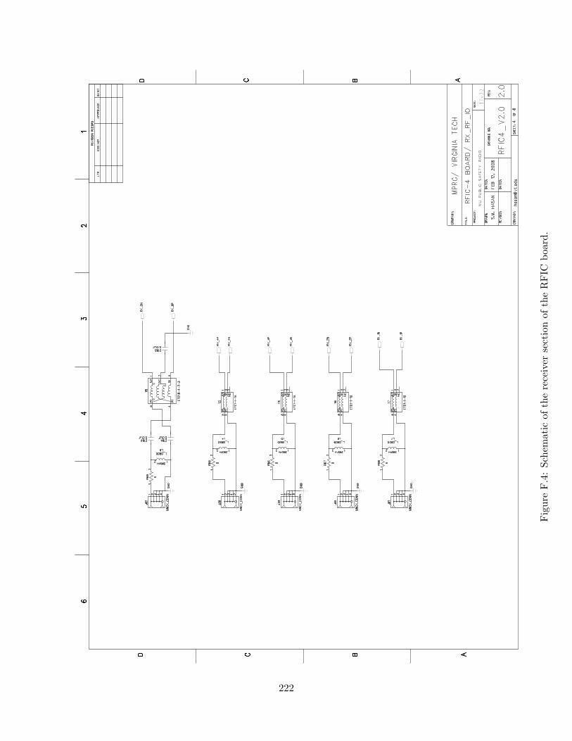
Fig
ure
F.4
:Sc
hem
atic
ofth
ere
ceiv
erse
ctio
nof
the
RFIC
boar
d.
222

Fig
ure
F.5
:Sc
hem
atic
ofth
etr
ansm
itte
rse
ctio
nof
the
RFIC
boar
d.
223

Fig
ure
F.6
:Sc
hem
atic
ofth
epo
wer
supp
lyse
ctio
nof
the
RFIC
boar
d.
224
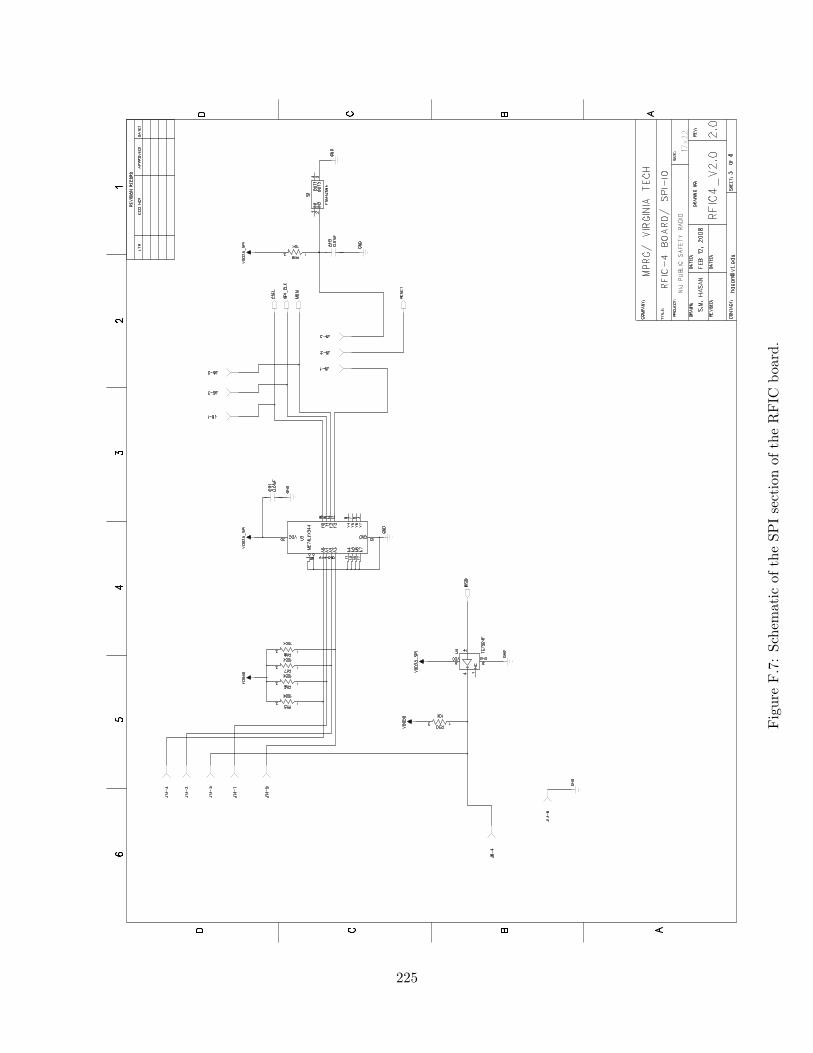
Fig
ure
F.7
:Sc
hem
atic
ofth
eSP
Ise
ctio
nof
the
RFIC
boar
d.
225

Fig
ure
F.8
:Top
laye
rof
the
RFIC
boar
d.
226
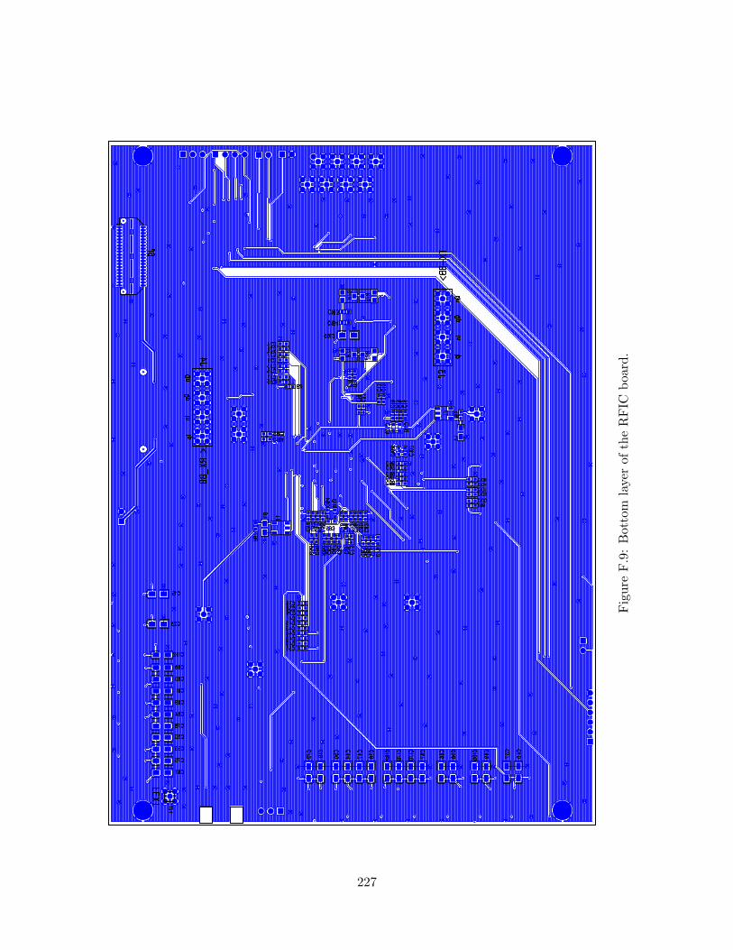
Fig
ure
F.9
:B
otto
mla
yer
ofth
eR
FIC
boar
d.
227

Fig
ure
F.1
0:Pow
erla
yer
ofth
eR
FIC
boar
d.
228
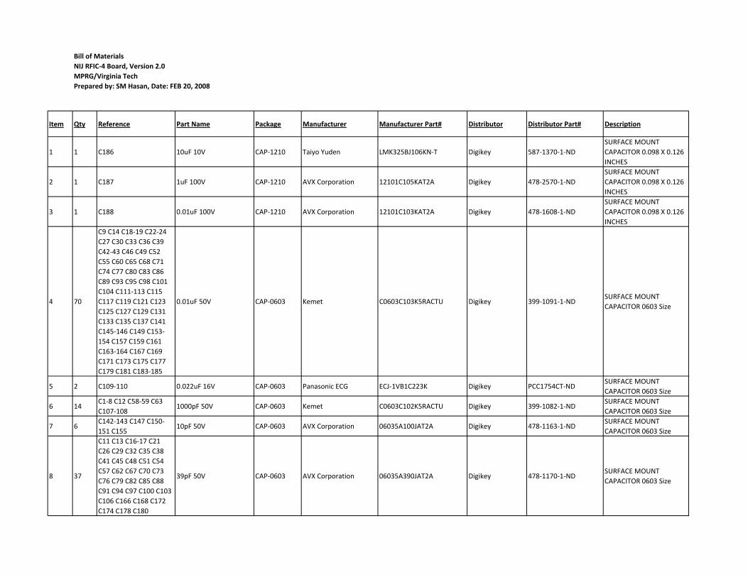
Bill of Materials
NIJ RFIC-4 Board, Version 2.0
MPRG/Virginia Tech
Prepared by: SM Hasan, Date: FEB 20, 2008
Item Qty Reference Part Name Package Manufacturer Manufacturer Part# Distributor Distributor Part# Description
1 1 C186 10uF 10V CAP-1210 Taiyo Yuden LMK325BJ106KN-T Digikey 587-1370-1-ND
SURFACE MOUNT
CAPACITOR 0.098 X 0.126
INCHES
2 1 C187 1uF 100V CAP-1210 AVX Corporation 12101C105KAT2A Digikey 478-2570-1-ND
SURFACE MOUNT
CAPACITOR 0.098 X 0.126
INCHES
3 1 C188 0.01uF 100V CAP-1210 AVX Corporation 12101C103KAT2A Digikey 478-1608-1-ND
SURFACE MOUNT
CAPACITOR 0.098 X 0.126
INCHES
4 70
C9 C14 C18-19 C22-24
C27 C30 C33 C36 C39
C42-43 C46 C49 C52
C55 C60 C65 C68 C71
C74 C77 C80 C83 C86
C89 C93 C95 C98 C101
C104 C111-113 C115
C117 C119 C121 C123
C125 C127 C129 C131
C133 C135 C137 C141
C145-146 C149 C153-
154 C157 C159 C161
C163-164 C167 C169
C171 C173 C175 C177
C179 C181 C183-185
0.01uF 50V CAP-0603 Kemet C0603C103K5RACTU Digikey 399-1091-1-NDSURFACE MOUNT
CAPACITOR 0603 Size
5 2 C109-110 0.022uF 16V CAP-0603 Panasonic ECG ECJ-1VB1C223K Digikey PCC1754CT-NDSURFACE MOUNT
CAPACITOR 0603 Size
6 14C1-8 C12 C58-59 C63
C107-1081000pF 50V CAP-0603 Kemet C0603C102K5RACTU Digikey 399-1082-1-ND
SURFACE MOUNT
CAPACITOR 0603 Size
7 6C142-143 C147 C150-
151 C15510pF 50V CAP-0603 AVX Corporation 06035A100JAT2A Digikey 478-1163-1-ND
SURFACE MOUNT
CAPACITOR 0603 Size
8 37
C11 C13 C16-17 C21
C26 C29 C32 C35 C38
C41 C45 C48 C51 C54
C57 C62 C67 C70 C73
C76 C79 C82 C85 C88
C91 C94 C97 C100 C103
C106 C166 C168 C172
C174 C178 C180
39pF 50V CAP-0603 AVX Corporation 06035A390JAT2A Digikey 478-1170-1-NDSURFACE MOUNT
CAPACITOR 0603 Size

Item Qty Reference Part Name Package Manufacturer Manufacturer Part# Distributor Distributor Part# Description
9 1 C64 6800pF 50V CAP-0603 Panasonic ECG ECJ-1VB1H682K Digikey PCC1782CT-NDSURFACE MOUNT
CAPACITOR 0603 Size
10 9
C92 C140 C144 C148
C152 C156 C158 C160
C162
10uF 6.3V CAP-0805 AVX Corporation 08056D106KAT2A Digikey 478-1417-1-NDSURFACE MOUNT
CAPACITOR 0805 Size
11 46
C10 C15 C20 C25 C28
C31 C34 C37 C40 C44
C47 C50 C53 C56 C61
C66 C69 C72 C75 C78
C81 C84 C87 C90 C96
C99 C102 C105 C114
C116 C118 C120 C122
C124 C126 C128 C130
C132 C134 C136 C138-
139 C165 C170 C176
C182
3.3uF 6.3VCAP-3216,
TANTRohm TCA0J335M8R Digikey 511-1440-1-ND CAP TANTALUM
12 1 C189 10uF 16VCAP_3216,
TANTRohm TCA1C106M8R Digikey 511-1473-1-ND CAP TANTALUM
13 1 J10CONN_SAM8123_SOCK
ETSocket Samtec Inc QSE-020-01-L-D-A Digikey SAM8123-ND High Speed Socket 40 pins
14 1 J9CONN_SAM8128_HEAD
ERPlug Samtec Inc QTE-020-01-X-D-A Digikey SAM8128-ND High Speed Plug 40 pins
15 4 T3 T5-7 ETC1-1-13 SM-22 MACOM ETC1-1-13Richardson
ElectronicsETC1-1-13 TRANSFORMER
16 2 T4 T8 ETC1.6-4-2-3 SM-22 MACOM ETC1.6-4-2-3Richardson
ElectronicsETC1.6-4-2-3
TRANSFORMER 500-2500
MHz
17 2 T1-2 ETC4-1T-7 SM-22 MACOM ETC4-1T-7Richardson
ElectronicsETC4-1T-7
TRANSFORMER 6-1000
MHz
18 2 R77-78 Pot 10K SMD Panasonic ECG EVN-5ESX50B14 Digikey P5E103CT-NDTRIMMER
POTENTIOMETER
19 4 R70-73 Pot 1K SMD Panasonic ECG EVN-5ESX50B13 Digikey P5E102CT-NDTRIMMER
POTENTIOMETER
20 1 S1 Switch Tact SMD Tyco Electronics FSM4JSMA Digikey 450-1129-ND
21 1 D1 LED, Green SMT LITE-ON LTST-C190GKT Digikey 160-1183-1-ND LIGHT EMITTING DIODE
22 1 L9 1.5nH L_0201 Coilcraft 0201CS-1N5XJLU Coilcraft 0201CS-1N5XJLUSurface Mount Inductor
0201 Size
23 3 L1-3 10nH L-0603 Coilcraft 0603CS-10NXJBW Coilcraft 0603CS-10NXJBWSurface Mount Inductor
0603 Size
24 5 L4-8 L_0805,390nH L-0805 Coilcraft 0805CS-391XJBC Coilcraft 0805CS-391XJBCSurface Mount Inductor
0805 Size
25 1 U2 MC74LVX244 TSSOP-20Fairchild
Semiconductor74LVX244MTCX Digikey 74LVX244MTCXCT-ND OCTAL BUS BUFFER
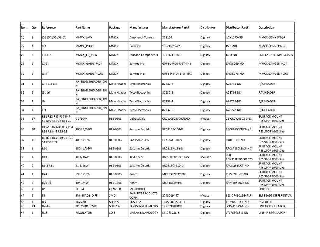
Item Qty Reference Part Name Package Manufacturer Manufacturer Part# Distributor Distributor Part# Description
26 8 J52 J54 J56 J58-62 MMCX_JACK MMCX Amphenol Connex 262104 Digikey ACX1275-ND MMCX CONNECTOR
27 1 J24 MMCX_PLUG MMCX Emerson 135-3801-201 Digikey J601-ND MMCX CONNECTOR
28 2 J12 J15 MMCX_EL_JACK MMCX Johnson Components 135-3711-801 Digikey J603-ND END LAUNCH MMCX JACK
29 2 J1-2 MMCX_GANG_JACK MMCX Samtec Inc GRF1-J-P-04-E-ST-TH1 Digikey SAM8069-ND MMCX GANGED JACK
30 2 J3-4 MMCX_GANG_PLUG MMCX Samtec Inc GRF1-P-P-04-E-ST-TH1 Digikey SAM8076-ND MMCX GANGED PLUG
31 4 J7-8 J11 J13RA_SINGLEHEADER_2PI
NMale Header Tyco Electronics 87232-2 Digikey A28764-ND R/A HEADER
32 2 J5 J16RA_SINGLEHEADER_3PI
NMale Header Tyco Electronics 87232-3 Digikey A28766-ND R/A HEADER
33 1 J6RA_SINGLEHEADER_4PI
NMale Header Tyco Electronics 87232-4 Digikey A28768-ND R/A HEADER
34 1 J14RA_SINGLEHEADER_6PI
NMale Header Tyco Electronics 87232-6 Digikey A28772-ND R/A HEADER
35 17R31 R33 R35 R37 R47-
50 R59 R61-62 R64-690 1/10W RES-0603 Vishay/Dale CRCW06030000Z0EA Mouser 71-CRCW0603-0-E3
SURFACE MOUNT
RESISTOR 0603 Size
36 30R15-18 R21-30 R32 R34
R36 R38-46 R55-58100K 1/16W RES-0603 Sasumu Co Ltd. RR0816P-104-D Digikey RR08P100KDCT-ND
SURFACE MOUNT
RESISTOR 0603 Size
37 11R9 R12 R14 R19-20 R51-
54 R60 R6310K 1/16W RES-0603 Panasonic ECG ERA-3AEB103V Digikey P10KDBCT-ND
SURFACE MOUNT
RESISTOR 0603 Size
38 1 R10 150K 1/16W RES-0603 Sasumu Co Ltd. RR0816P-154-D Digikey RR08P150KDCT-NDSURFACE MOUNT
RESISTOR 0603 Size
39 1 R13 1K 1/16W RES-0603 KOA Speer RN731JTTD1001B25 Mouser660-
RN731JTTD1001B25
SURFACE MOUNT
RESISTOR 0603 Size
40 9 R1-8 R11 51 1/16W RES-0603 Sasumu Co Ltd. RR0816Q-510-D Digikey RR08Q51DCT-NDSURFACE MOUNT
RESISTOR 0603 Size
41 1 R74 698 1/10W RES-0603 Rohm MCR03EZPFX6980 Digikey RHM698HCT-NDSURFACE MOUNT
RESISTOR 0603 Size
42 2 R75-76 10K 1/4W RES-1206 Rohm MCR18EZPJ103 Digikey RHM10KERCT-NDSURFACE MOUNT
RESISTOR 0603 Size
43 1 U1 RFIC-4 QFN-100 MOTOROLA SDR RFIC
44 1 E1 SM_BEADS_DIFF SMDFAIR-RITE PRODUCTS
CORP2743019447 Mouser 623-2743019447LF SM BEADS DIFFERENTIAL
45 1 U3 TC7S04F SSOP-5 TOSHIBA TC7S04F(T5L,F,T) Digikey TC7S04FTFCT-ND INVERTER
46 13 U4-16 TPS76901DBVR SOT-23-5 TEXAS INSTRUMENTS TPS76901DBVR Digikey 296-11029-1-ND LINEAR REGULATOR
47 1 U18 REGULATOR SO-8 LINEAR TECHNOLOGY LT1763CS8-5 Digikey LT1763CS8-5-ND LINEAR REGULATOR
Appendix G
ADC/DAC Board
This appendix documents the design of the ADC/DAC board for the VT MMR discussed in Sec-
tion 7.5.3 (“ADC/DAC Board”). This board also contains a frequency synthesizer to supply 1 GHz
reference to the RFIC board.
G.1 Board Overview
Figure G.1 and Table G.1 present all the input/output ports of the ADC/DAC board.
Figure G.2 shows the schematic of the ADC section in the ADC/DAC board. The AD9248 dual
14-bit A/D converter from Analog Devices has been selected to convert the analog signal to digital
signal in our design to operate the receiver section. The differential in-phase (I) and quadrature-
phase (Q) inputs are applied to the input ports of the ADCs. Although this ADC has two output
ports (data port A and data port B), the output data from the dual ADCs can be multiplexed onto
a single output port. In our case only data port B is enabled to supply the multiplexed digitized
signals from the two ADCs. The FPGA board shown in Figure 7.11 supplies the reference clock for
both of the A/D converters through the ADI connector in this IC. There is also an option to supply
reference clock from external source other than the FPGA board. The data port B is connected to
a 40-pin connector (J1) through two octal bus buffer ICs (74VHC541) and 22 ohm resistor pads.
The unused data port A is terminated with 22 ohm resistors and connected to a 40-pin header
232

ADC/DAC Board
Rx/Tx Board Overview
IB
DAC Output
ADC Input
ADI Interface to
FPGA Board
EXT_CLK_DAC
CLK_ADC
IA
QB
QA
IA
IB
QB
QA
Figure G.1: Summary of the ADC/DAC board I/O.
Table G.1: Description of input/output ports of the ADC/DAC board.
Function Port Name Conn. Name CharacteristicsDAC Output IB J8-A Differential Output
IA J8-B of I-ChannelQB J8-C Differential OutputQA J8-D of Q-Channel
ADC Input IA J24-A Differential InputIB J24-B of I-ChannelQB J24-C Differential InputQA J24-D of Q-Channel
CLK ADC Input CLK ADC J5 ADC Reference Clock (4 MHz)CLK DAC Input EXT CLK J9 External DAC Clock (4 MHz)Synthesizer Out-put
RF OUT J27 RF analog output from the synthesizer(50Ω, +10 dBm)
ADI Interface ADI J1, J12 ADI interface to FPGA
233

connector (J11).
Figure G.3 shows the circuit diagram of the DAC section in the ADC/DAC board. The AD9761
dual 10-bit D/A converter from Analog Devices has been selected to convert the digital signal
to analog signal in our design for the transmission operation. Similar to the ADC section, the
DAC provides the differential in-phase (I) and quadrature-phase (Q) analog output signals from
the digital I and Q input signal. Similar to the ADC section, the reference clock is supplied from
an FPGA board through the ADI connectors. This also has an option to receive reference clock
from external source other than the FPGA board. The input of the data port is connected to a
40-pin connector (J12) through 22 ohm resistor pads.
Figure G.4 shows the schematic of the power supply section in the ADC/DAC board.Three separate
3V supply voltages and one 2.5V supply voltage for ADC, and two separate 5V supply voltages
for DAC have been created from a single 10V power source. First, the main 10V input voltage is
fed into a 3A low–dropout regulator IC (LT1529) to create a 5V positive voltage. This 5V voltage
is supplied to the input of the four low–dropout regulator ICs (ADP3339), which provides the
required output voltage of 3V and 2.5V. Two positive voltage regulator ICs MC78M05 generate
the 5V supply voltages for the DAC directly from the 10V power supply.
Figure G.5 shows the schematic of the synthesizer section. We use a frequency synthesizer, Model
LFSW35105-100, from Synergy Microwave Corporation1. This synthesizer is capable of providing
frequency output 350 to 1050 MHz using just a single 10 MHz ( 1 Vpp to 3 Vpp) reference frequency.
The FPGA board shown in Figure 7.11 contains a DAC, which is used to supply this 10 MHz
reference signal to the synthesizer.
Table G.2 shows the jumper settings of the PCB.
A summary of the cost for one ADC/DAC board is given in Table G.3. Since we prepared just
two boards for the present study using the quickest manufacturing time, the PCB fabrication and
assembly cost is not representative of the cost to build the same device in large quantities.
1http://www.synergymwave.com
234
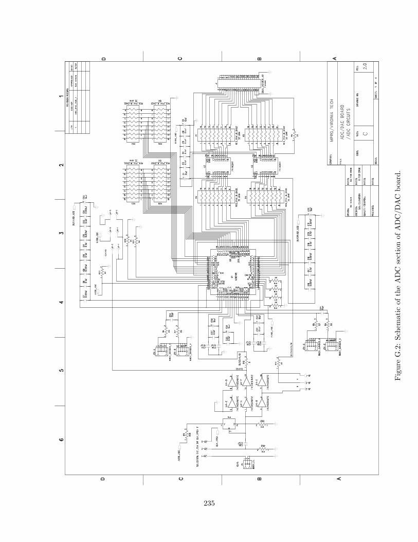
Fig
ure
G.2
:Sc
hem
atic
ofth
eA
DC
sect
ion
ofA
DC
/DA
Cbo
ard.
235

Fig
ure
G.3
:Sc
hem
atic
ofth
eD
AC
sect
ion
ofA
DC
/DA
Cbo
ard.
236

Fig
ure
G.4
:Sc
hem
atic
ofth
epo
wer
supp
lyse
ctio
nof
AD
C/D
AC
boar
d.
237
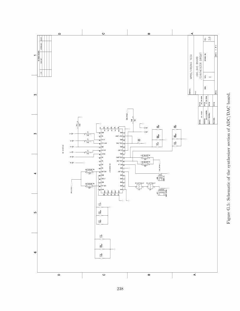
Fig
ure
G.5
:Sc
hem
atic
ofth
esy
nthe
size
rse
ctio
nof
AD
C/D
AC
boar
d.
238

Table G.2: Jumper settings of the ADC/DAC board.
Jumper Description Normal Setting CommentJ21 Power In 3V supply to ADCJ22 Power In 2.5V supply to ADCJ23 Power In 3V supply to ADCJ24 Power In 3V supply to ADCJ25 Power In 5V supply to DACJ26 Power In 5V supply to DACJ8 Mux Select Out Connect MUX SEL pin to ClockJ9 Mux Select Out Connect MUX SEL pin to VDDJ10 Mux Select In Connect MUX SEL pin to GNDJ7 Clock Polarity A Position B select the opposite polarityJ14 DAC Clock Select A ‘A’ selects the clock from the FPGA board
and ‘B’ selects the clock from an externalsource
G.2 Layout, and Bill of Materials
The PCB layout of the implemented ADC/DAC board is shown in Figures G.6 to G.8. The bill of
materials for this board is shown at the end of this appendix.
239
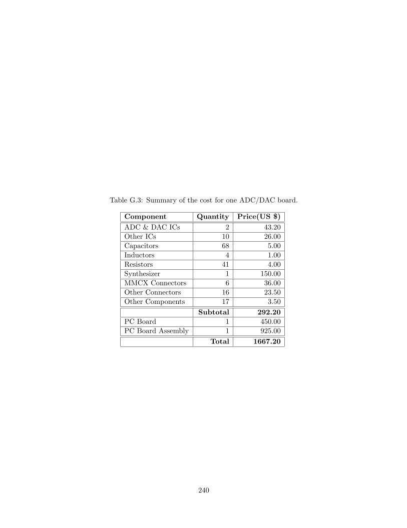
Table G.3: Summary of the cost for one ADC/DAC board.
Component Quantity Price(US $)ADC & DAC ICs 2 43.20Other ICs 10 26.00Capacitors 68 5.00Inductors 4 1.00Resistors 41 4.00Synthesizer 1 150.00MMCX Connectors 6 36.00Other Connectors 16 23.50Other Components 17 3.50
Subtotal 292.20PC Board 1 450.00PC Board Assembly 1 925.00
Total 1667.20
240

Fig
ure
G.6
:Top
laye
rof
the
AD
C/D
AC
boar
d.
241

Fig
ure
G.7
:B
otto
mla
yer
ofth
eA
DC
/DA
Cbo
ard.
242
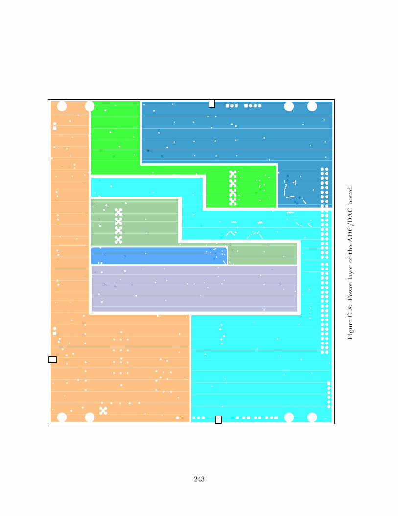
Fig
ure
G.8
:Pow
erla
yer
ofth
eA
DC
/DA
Cbo
ard.
243

Bill of Materials
NIJ ADC_DAC Board, Ver. 2.0
MPRG/Virginia Tech
Prepared By: S.M. Hasan, Date: FEB 20, 2008
Item Qty Reference Part Name Package Manufacturer Manufacturer Part# Distributor Distributor Part# Description
1 2 U2-3 74VHC541 20-SOL TOSHIBA TC74VHC541FW Digikey TC74VHC541FW-ND OCTAL BUS BUFFER
2 1 U4 74VHC04MTC 14-TSSOPFAIRCHILD
SEMICONDUCTOR74VHC04MTC Digikey 74VHC04MTC-ND HEX INVERTER
3 1 U8 AD3339,2.5V SOT-223 Analog Devices ADP3339AKCZ-2.5-R7 Digikey ADP3339AKCZ-2.5-R7CT-ND Low Dropout Regulator
4 3 U7 U9-10 AD3339,3V SOT-223 Analog Devices ADP3339AKCZ-3-RL7 Digikey ADP3339AKCZ-3-RL7CT-ND Low Dropout Regulator
5 1 U1 AD9248 64-LQFP Analog Devices AD9248BSTZ-20 Digikey AD9248BSTZ-20-ND14-Bit Dual A/D
Converter
6 1 U5 AD9761 28-SSOP ANALOG DEVICES AD9761ARSZ Digikey AD9761ARSZ-ND DUAL 10-BIT DAC
7 2 A1-2 Attenuator MMM168 Minicircuits LAT-10+ Minicircuits LAT-10+ SMD Fixed Attenuator
8 2 C74 C77 0.01uF 100V CAP_1210 AVX Corporation 12101C103KAT2A Digikey 478-1608-1-ND
SURFACE MOUNT
CAPACITOR 0.098 X 0.126
INCHES
9 2 C57 C76 1uF 100V CAP_1210 AVX Corporation 12101C105KAT2A Digikey 478-2570-1-ND
SURFACE MOUNT
CAPACITOR 0.098 X 0.126
INCHES
10 7C7 C9 C12 C14 C16 C18
C210.001uF CAP_0603 Panasonic-ECG ECJ-1VB1H102K Digikey PCC1772CT-ND
SURFACE MOUNT
CAPACITOR 0603 Size
11 19
C8 C10-11 C13 C17 C19-
20 C25-27 C29-31 C33
C37-38 C41-42 C45
0.1uF CAP_0603 Murata Electronics GRM188R71H104KA93D Digikey 490-1519-1-NDSURFACE MOUNT
CAPACITOR 0603 Size
12 4 C58 C78 C80 C82 1000pF 50V CAP_0603 AVX Corporation 06035C102KAT2A Digikey 478-1215-1-NDSURFACE MOUNT
CAPACITOR 0603 Size
13 4 C75 C79 C81 C83 100pF 50V CAP_0603 AVX Corporation 06035A101KAT2A Digikey 478-3717-1-NDSURFACE MOUNT
CAPACITOR 0603 Size
14 1 C36 1uF CAP_0603 Panasonic-ECG ECJ-1VB1C105K Digikey PCC2224CT-NDSURFACE MOUNT
CAPACITOR 0603 Size
15 4 C70-73 2.2uF 10V CAP_0603 Panasonic-ECG ECJ-1VB1A225K Digikey PCC2397CT-NDSURFACE MOUNT
CAPACITOR 0603 Size
16 6 C23-24 C39-40 C43-44 20pF CAP_0603 Murata Electronics GRM1885C2A200JA01D Digikey 490-1334-1-NDSURFACE MOUNT
CAPACITOR 0603 Size
17 5 C3-6 C35 0.1uF CAP_0805 Kemet C0805C104K5RACTU Digikey 399-1170-1-NDSURFACE MOUNT
CAPACITOR 0805 Size
18 4 C63 C65-66 C68 0.1uF CAP_1206 Kemet C1206C104K5RACTU Digikey 399-1249-1-NDSURFACE MOUNT
CAPACITOR 1206 Size
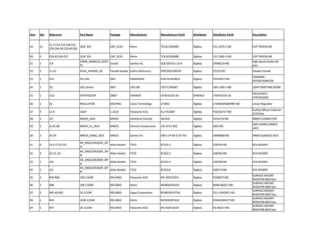
Item Qty Reference Part Name Package Manufacturer Manufacturer Part# Distributor Distributor Part# Description
19 21C1-2 C15 C22 C28 C32
C34 C46-56 C59-60 C6910uF 16V CAP_3216 Rohm TCA1C106M8R Digikey 511-1473-1-ND CAP TANTALUM
20 4 C61-62 C64 C67 22uF 10V CAP_3216 Rohm TCA1A226M8R Digikey 511-1465-1-ND CAP TANTALUM
21 1 J14CONN_SAM8123_SOCK
ETSocket Samtec Inc QSE-020-01-L-D-A Digikey SAM8123-ND
High Speed Socket 40
pins
22 2 J1 J12 DUAL_HEADER_40 Female Header Sullins Electronics PPPC202LFBN-RC Digikey S7123-ND Header Female
23 1 R15 Pot 10K SMT PANASONIC EVN-5ESX50B14 Digikey P5E103CT-NDTRIMMER
POTENTIOMETER
24 1 D1 LED, Green SMT LITE-ON LTST-C190GKT Digikey 160-1183-1-ND LIGHT EMITTING DIODE
25 1 U13 SYNTHESIZER 280LF SYNERGY LFSW35105-50 SYNERGY LFSW35105-50FREQUENCY
SYNTHESIZER
26 1 E2 REGULATOR MSOP8G Linear Technology LT1965 Digikey LT1965IMS8E#PBF-ND Linear Regulator
27 4 L1-4 10uH L-1210 Panasonic-ECG ELJ-FA100JF Digikey PCD1817CT-NDSurface Mount Inductor
1210 Size
28 1 J27 MMCX_JACK MMCX Amphenol Connex 262104 Digikey ACX1275-ND MMCX CONNECTOR
29 3 J5 J9 J28 MMCX_EL_JACK MMCX Johnson Components 135-3711-801 Digikey J603-NDEND LAUNCH MMCX
JACK
30 2 J8 J24 MMCX_GANG_JACK MMCX Samtec Inc GRF1-J-P-04-E-ST-TH1 Digikey SAM8069-ND MMCX GANGED JACK
31 6 J2-4 J7 J13 J22RA_SINGLEHEADER_2PI
NMale Header TYCO 87232-2 Digikey A28764-ND R/A HEADER
32 3 J6 J11 J15RA_SINGLEHEADER_3PI
NMale Header TYCO 87232-3 Digikey A28766-ND R/A HEADER
33 1 J10RA_SINGLEHEADER_4PI
NMale Header TYCO 87232-4 Digikey A28768-ND R/A HEADER
34 1 J21RA_SINGLEHEADER_6PI
NMale Header TYCO 87232-6 Digikey A28772-ND R/A HEADER
35 2 R36 R40 100 1/10W RES-0603 Panasonic-ECG ERJ-3GEYJ101V Digikey P100GCT-NDSURFACE MOUNT
RESISTOR 0603 Size
36 1 R48 10K 1/10W RES-0603 Rohm MCR03EZPJ103 Digikey RHM10KGCT-NDSURFACE MOUNT
RESISTOR 0603 Size
37 3 R42-43 R45 1K 1/10W RES-0603 Yageo Corporation RC0603JR-071KL Digikey 311-1.0KGRCT-NDSURFACE MOUNT
RESISTOR 0603 Size
38 1 R44 220K 1/10W RES-0603 Rohm MCR03EZPJ224 Digikey RHM220KGCT-NDSURFACE MOUNT
RESISTOR 0603 Size
39 1 R37 2K 1/10W RES-0603 Panasonic-ECG ERJ-3GEYJ202V Digikey P2.0KGCT-NDSURFACE MOUNT
RESISTOR 0603 Size
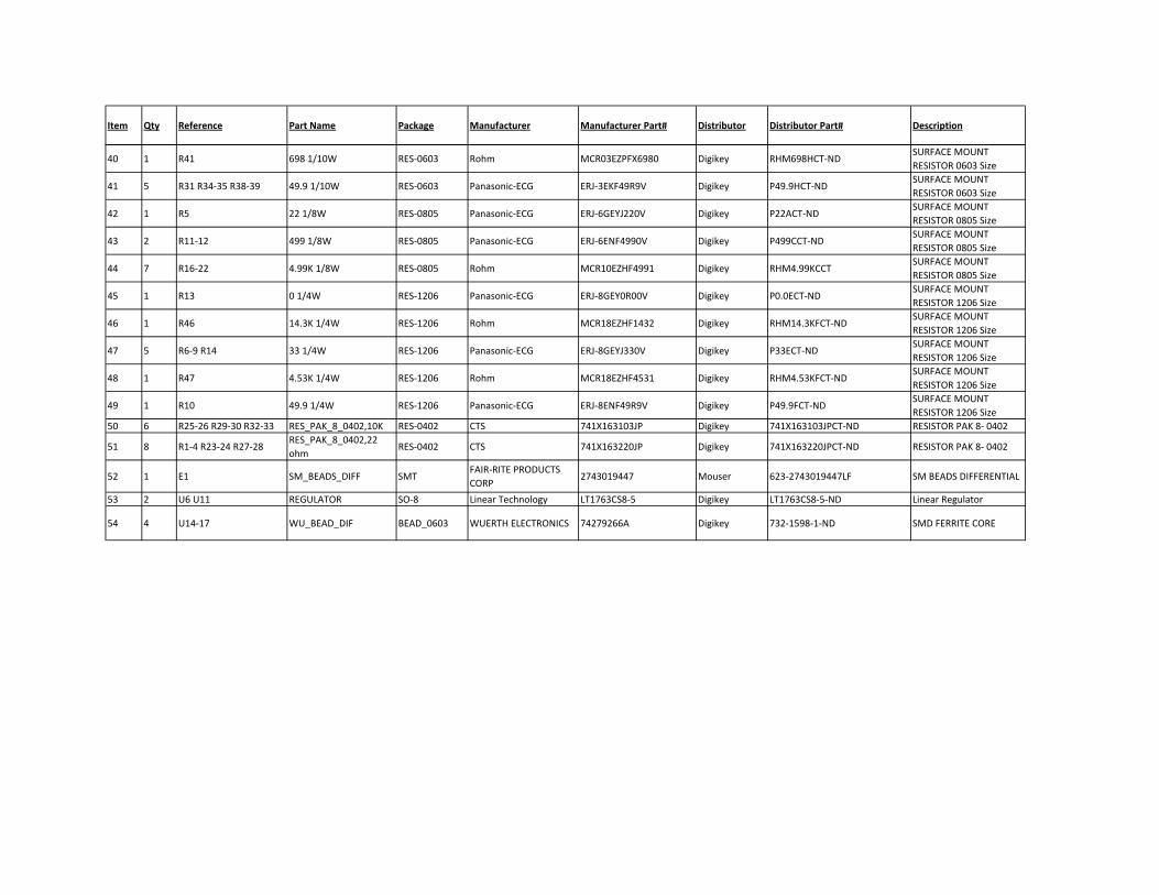
Item Qty Reference Part Name Package Manufacturer Manufacturer Part# Distributor Distributor Part# Description
40 1 R41 698 1/10W RES-0603 Rohm MCR03EZPFX6980 Digikey RHM698HCT-NDSURFACE MOUNT
RESISTOR 0603 Size
41 5 R31 R34-35 R38-39 49.9 1/10W RES-0603 Panasonic-ECG ERJ-3EKF49R9V Digikey P49.9HCT-NDSURFACE MOUNT
RESISTOR 0603 Size
42 1 R5 22 1/8W RES-0805 Panasonic-ECG ERJ-6GEYJ220V Digikey P22ACT-NDSURFACE MOUNT
RESISTOR 0805 Size
43 2 R11-12 499 1/8W RES-0805 Panasonic-ECG ERJ-6ENF4990V Digikey P499CCT-NDSURFACE MOUNT
RESISTOR 0805 Size
44 7 R16-22 4.99K 1/8W RES-0805 Rohm MCR10EZHF4991 Digikey RHM4.99KCCTSURFACE MOUNT
RESISTOR 0805 Size
45 1 R13 0 1/4W RES-1206 Panasonic-ECG ERJ-8GEY0R00V Digikey P0.0ECT-NDSURFACE MOUNT
RESISTOR 1206 Size
46 1 R46 14.3K 1/4W RES-1206 Rohm MCR18EZHF1432 Digikey RHM14.3KFCT-NDSURFACE MOUNT
RESISTOR 1206 Size
47 5 R6-9 R14 33 1/4W RES-1206 Panasonic-ECG ERJ-8GEYJ330V Digikey P33ECT-NDSURFACE MOUNT
RESISTOR 1206 Size
48 1 R47 4.53K 1/4W RES-1206 Rohm MCR18EZHF4531 Digikey RHM4.53KFCT-NDSURFACE MOUNT
RESISTOR 1206 Size
49 1 R10 49.9 1/4W RES-1206 Panasonic-ECG ERJ-8ENF49R9V Digikey P49.9FCT-NDSURFACE MOUNT
RESISTOR 1206 Size
50 6 R25-26 R29-30 R32-33 RES_PAK_8_0402,10K RES-0402 CTS 741X163103JP Digikey 741X163103JPCT-ND RESISTOR PAK 8- 0402
51 8 R1-4 R23-24 R27-28RES_PAK_8_0402,22
ohmRES-0402 CTS 741X163220JP Digikey 741X163220JPCT-ND RESISTOR PAK 8- 0402
52 1 E1 SM_BEADS_DIFF SMTFAIR-RITE PRODUCTS
CORP2743019447 Mouser 623-2743019447LF SM BEADS DIFFERENTIAL
53 2 U6 U11 REGULATOR SO-8 Linear Technology LT1763CS8-5 Digikey LT1763CS8-5-ND Linear Regulator
54 4 U14-17 WU_BEAD_DIF BEAD_0603 WUERTH ELECTRONICS 74279266A Digikey 732-1598-1-ND SMD FERRITE CORE
Appendix H
Audio Board & User Interface
This appendix documents the design of the audio board and the user interface implemented for the
VT MMR prototype.
Figure H.1 shows the audio board. This board has an interface to connect a hand–held push–
to–talk (PTT) type of microphone and speaker and contains a volume control for speaker and
microphone. It also has internal circuitry to the detect the PTT signal, so that whenever the PTT
button is pressed, the radio configures itself for transmit mode. Figure H.2 shows the schematic of
the audio board. The PCB layout of the implemented audio board is shown in Figure H.3. The
bill of materials for this board is shown at the end of this section.
247

Figure H.1: Audio board.
248
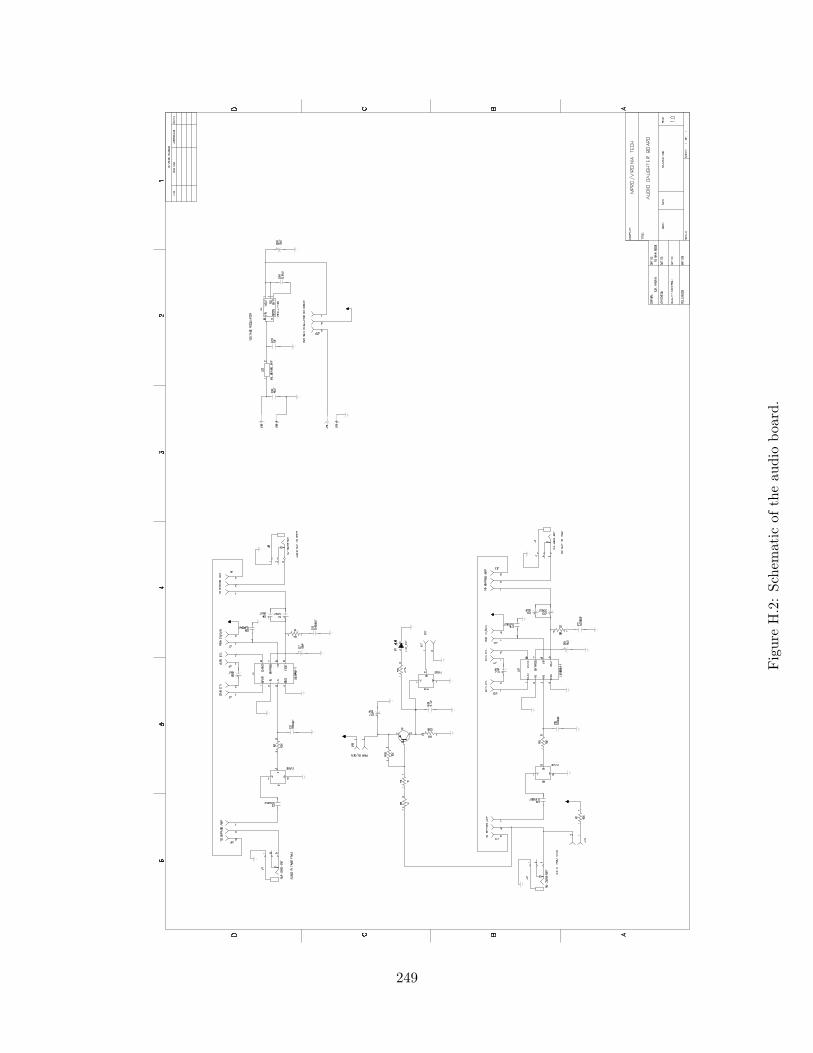
Fig
ure
H.2
:Sc
hem
atic
ofth
eau
dio
boar
d.
249

Fig
ure
H.3
:Top
laye
rof
the
audi
obo
ard.
250
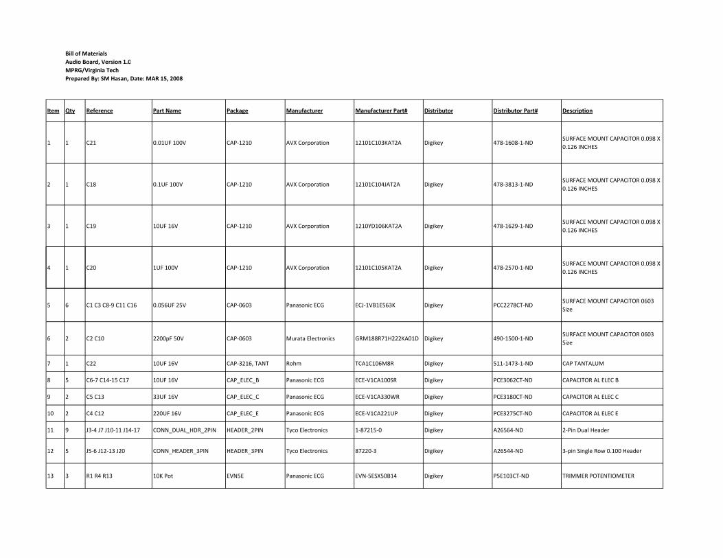
Bill of Materials
Audio Board, Version 1.0
MPRG/Virginia Tech
Prepared By: SM Hasan, Date: MAR 15, 2008
Item Qty Reference Part Name Package Manufacturer Manufacturer Part# Distributor Distributor Part# Description
1 1 C21 0.01UF 100V CAP-1210 AVX Corporation 12101C103KAT2A Digikey 478-1608-1-NDSURFACE MOUNT CAPACITOR 0.098 X
0.126 INCHES
2 1 C18 0.1UF 100V CAP-1210 AVX Corporation 12101C104JAT2A Digikey 478-3813-1-NDSURFACE MOUNT CAPACITOR 0.098 X
0.126 INCHES
3 1 C19 10UF 16V CAP-1210 AVX Corporation 1210YD106KAT2A Digikey 478-1629-1-NDSURFACE MOUNT CAPACITOR 0.098 X
0.126 INCHES
SURFACE MOUNT CAPACITOR 0.098 X 4 1 C20 1UF 100V CAP-1210 AVX Corporation 12101C105KAT2A Digikey 478-2570-1-ND
SURFACE MOUNT CAPACITOR 0.098 X
0.126 INCHES
5 6 C1 C3 C8-9 C11 C16 0.056UF 25V CAP-0603 Panasonic ECG ECJ-1VB1E563K Digikey PCC2278CT-NDSURFACE MOUNT CAPACITOR 0603
Size
6 2 C2 C10 2200pF 50V CAP-0603 Murata Electronics GRM188R71H222KA01D Digikey 490-1500-1-NDSURFACE MOUNT CAPACITOR 0603
Size
7 1 C22 10UF 16V CAP-3216, TANT Rohm TCA1C106M8R Digikey 511-1473-1-ND CAP TANTALUM
8 5 C6-7 C14-15 C17 10UF 16V CAP_ELEC_B Panasonic ECG ECE-V1CA100SR Digikey PCE3062CT-ND CAPACITOR AL ELEC B
9 2 C5 C13 33UF 16V CAP_ELEC_C Panasonic ECG ECE-V1CA330WR Digikey PCE3180CT-ND CAPACITOR AL ELEC C
10 2 C4 C12 220UF 16V CAP_ELEC_E Panasonic ECG ECE-V1CA221UP Digikey PCE3275CT-ND CAPACITOR AL ELEC E
11 9 J3-4 J7 J10-11 J14-17 CONN_DUAL_HDR_2PIN HEADER_2PIN Tyco Electronics 1-87215-0 Digikey A26564-ND 2-Pin Dual Header
12 5 J5-6 J12-13 J20 CONN_HEADER_3PIN HEADER_3PIN Tyco Electronics 87220-3 Digikey A26544-ND 3-pin Single Row 0.100 Header
13 3 R1 R4 R13 10K Pot EVN5E Panasonic ECG EVN-5ESX50B14 Digikey P5E103CT-ND TRIMMER POTENTIOMETER

14 1 D1 LED Green Clear LED_PAD LITE-ON LTST-C190GKT Digikey 160-1183-1-ND LIGHT EMITTING DIODE
15 2 U1-2 LM386M-1 SO-8NATIONAL
SEMICONDUCTORLM386M-1/NOPB Digikey LM386M-1-ND AUDIO POWER AMPLIFIER
16 1 J2 MJ-2523-SMT MJ-2523-SMT CUI Inc MJ-2523-SMT Digikey CP-2523MJCT-ND2.5mm SURFACE MOUNT AUDIO JACK
MONO
17 1 J8 MJ-3523-SMT MJ-3523-SMT CUI Inc MJ-3523-SMT Digikey CP-3523MJCT-ND2.5mm SURFACE MOUNT AUDIO JACK
MONO
18 2 J1 J9 MJ1-3510-SMT MJ1-3510-SMT CUI Inc MJ1-3510-SMT Digikey CP1-3510MJCT-ND
19 1 Q1 MMBT3906LT1 SOT23 ON Semiconductor MMBT3906LT1G Digikey MMBT3906LT1GOSCT-NDGENERAL PURPOSE PNP SILICON
TRANSISTOR
20 2 J18-19 RA_SINGLEHEADER_2PIN SINGLEHEADER_2 TYCO 87232-2 Digikey A28764-ND 2-Pin R/A Single Row Header
21 2 R3 R6 10 1/4W RES-1206 Rohm MCR18EZPJ100 Digikey A28764-ND SURFACE MOUNT RESISTOR 1206 Size21 2 R3 R6 10 1/4W RES-1206 Rohm MCR18EZPJ100 Digikey A28764-ND SURFACE MOUNT RESISTOR 1206 Size
22 1 R11 100K 1/4W RES-1206 Rohm MCR18EZPF1003 Digikey RHM100KFRCT-ND SURFACE MOUNT RESISTOR 1206 Size
23 4 R2 R5 R7 R10 10K 1/4W RES-1206 Rohm MCR18EZPJ103 Digikey RHM10KERCT-ND SURFACE MOUNT RESISTOR 1206 Size
24 2 R8-9 1K 1/4W RES-1206 Rohm MCR18EZPF1001 Digikey RHM1.00KFRCT-ND SURFACE MOUNT RESISTOR 1206 Size
25 1 R12 470 1/4W RES-1206 Rohm MCR18EZPF4700 Digikey RHM470FRCT-ND SURFACE MOUNT RESISTOR 1206 Size
26 1 U3 SM_BEADS_DIFF SM_BEADSFAIR-RITE PRODUCTS
CORP2743019447 Mouser 623-2743019447LF SM BEADS DIFFERENTIAL
27 1 U4 VREG_LT1763 SO-8 Linear Technology LT1763CS8-5 Digikey LT1763CS8-5-ND Linear Regulator

A detailed description of the user interface designed for the VT MMR prototype appears in [100].
Figure H.4 shows the image of the embedded controller (Gumstix “LCD pack” 1) including the
touchscreen LCD interface which is used as the user interface for controlling the VT MMR. See
Figure 7.1 for this is it appears installed in the radio.
The Gumstix controller communicates with the RFIC through the serial peripheral interface (SPI)
and it also sends the multiplexer channel select information to the FPGA. In SPI communication the
Gumstix controller act as the master and the RFIC act as the slave. General-purpose input/output
(GPIO) pins in the Gumstix controller are used to perform this SPI operation. Generally, data can
be transferred in both directions simultaneously when the slave select signal is low active. However,
SPI communication in this design is only one way at current stage. That is why the signal MISO in
Figure H.5 is connected with the dotted line. The signal RESET shown in Figure H.5 is required
to reset the RFIC before starting to program it.
The Gumstix controller selects a channel and sends the corresponding channel information to the
FPGA board. The FPGA board processes the channel information and then sends them to the
RFFE board. Table H.1 is the truth table for the channel selection. Table H.2 shows the GPIO
pin mapping.
1http://www.gumstix.com
253
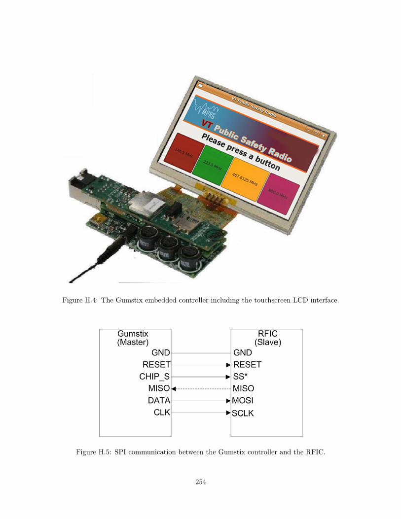
Figure H.4: The Gumstix embedded controller including the touchscreen LCD interface.
Figure 3: Assembly Drawinga
ahttp://gumstix.com/anim/LCDpack.swf
input/output (GPIO) pins to generate slave select signals in the given timeintervals. Generally, data can be transferred in both directions simultane-ously when the slave select signal is low active. However, SPI communicationin this report is only one way at current stage. That is why the signal MISOin Figure 4 is connected with the dotted line. The signal RESET in Figure 4is not defined in SPI bus, but it is required by the RFIC chip as the resetoperation is needed before reprogramming the RFIC chip.
Figure 4: SPI communication between Gumstix and RFIC
The Gumstix selects a channel and sends the corresponding channel in-formation to the FPGA board. The FPGA board processes the channel
5
Figure H.5: SPI communication between the Gumstix controller and the RFIC.
254
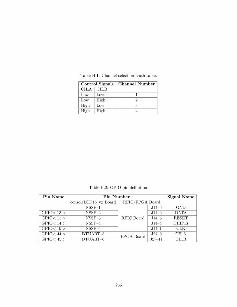
Table H.1: Channel selection truth table.
Control Signals Channel NumberCH A CH BLow Low 1Low High 2High Low 3High High 4
Table H.2: GPIO pin definition.
Pin Name Pin Number Signal NameconsoleLCD16–vx Board RFIC/FPGA Board
NSSP–1
RFIC Board
J14–6 GNDGPIO< 13 > NSSP–2 J14–2 DATAGPIO< 11 > NSSP–3 J14–5 RESETGPIO< 14 > NSSP–4 J14–4 CHIP SGPIO< 19 > NSSP–6 J14–1 CLKGPIO< 44 > BTUART–5
FPGA BoardJ27–9 CH A
GPIO< 45 > BTUART–6 J27–11 CH B
255

Appendix I
Copyright Permissions
Permission from Bitwave for the Figure 1.1
Date: Fri, 27 Feb 2009 08:09:40 -0500From: Russell Cyr <[email protected]>To: "S. Hasan" <[email protected]>Subject: Re: [Important] Permission to use a Figure
Dear Hasan:
You may use the figure as provided to us in your dissertation. Goodluck. Once it is published, we would very much like to read your thesis.
Best RegardsRuss
Russell J CyrCMO & Co-founderBitWave Semiconductor(O) +1.978.888.0202(C.) +1.978.697.1882(E) [email protected] Chelmsford Street, T3-7Lowell, MA 01851
256

Permission from Motorola for the Figure 2.17
Date: Thu, 12 Feb 2009 14:54:30 -0500From: Cafaro Gio-FNC013 <[email protected]>To: [email protected]: RE: Regarding the use of a Figure from your Paper
You have permission to use the figure. You should be able turn this intoa higher res picture. Good luck with the dissertation.
Gio
Permission from Antenna Factor for the Figure 6.12
Date: Thu, 26 Feb 2009 21:59:00 -0800From: Paul True <[email protected]>To: [email protected]: RE: [Important] Permission to use of a Figure from a Datasheet
Thanks for asking. We would appreciate a notation of Linx as the sourceof the image and with that you are granted permission to use it for thepurpose specified below. All the best on your dissertation.
Best Regards,
Paul TrueAntenna Factor Division &Linx Technologies, Inc.159 Ort LaneMerlin, OR 97532
257

Bibliography
[1] J. H. Reed, Software Radio: A Modern Approach to Radio Engineering, 1st ed. UpperSaddle River, NJ: Prentice Hall, 2002.
[2] National Institute of Justice, “Why Can’t We Talk? Working Together To Bridge theCommunications Gap To Save Lives : A Guide for Public Officials,” Feb. 2003. [Online].Available: http://www.ojp.usdoj.gov/nij/pubs-sum/204348.htm
[3] S. W. Ellingson and S. M. Hasan, “What’s in Radios Future?: All-band, all-mode radio couldsolve interoperability challenges.” Mission Critical Communications, vol. 22, no. 3, pp. 50–60,Mar. 2007.
[4] Joint Tactical Radio System. [Online]. Available: http://jtrs.army.mil
[5] J. Ryynanen et al., “Integrated Circuits for Multi–Band Multi–Mode Receivers,” IEEE Cir-cuits and Systems Magazine, vol. 6, no. 2, pp. 5–16, 2006.
[6] R. I. Desourdis Jr. et al., Emerging Public Safety Wireless Communication Systems, 1st ed.Norwood, MA: Artech House, 2001.
[7] SAFECOM Program, “Statement of Requirements for Public Safety Wireless Communica-tions & Interoperability,” U.S. Dept. of Homeland Security, Jan. 2003, ver. 1.1.
[8] Telecommunications Industry Association, Land Mobile FM or PM – Communications Equip-ment – Measurement and Performance Standards, Std. TIA-603-C, Dec. 2004.
[9] ——, Project 25 – Land Mobile Radio Transceiver Performance Recommendations – Project25 – Digital Radio Technology, C4FM/CQPSK Modulation, Std. TIA-102.CAAB-A, Sep.2002.
[10] ——, Radio Communications – Public Safety Wideband Data Equipment – Performance Mea-surement Procedures, Std. TIA-902.CAAA, Feb. 2003.
[11] Software Defined Radio (SDR) Forum, “Software Defined Radio Technology for PublicSafety,” Apr. 2006, SDRF-06-A-0001-V0.00. [Online]. Available: http://www.sdrforum.org
[12] J. Heaps, “Software Defined Radios Help Agencies Communicate,” National Institute ofJustice, Mar. 2008, NCJ 221504. [Online]. Available: http://nij.ncjrs.gov/publications/Pub Search.asp?category=99&searchtype=basic&location=top&PSID=36
258

[13] VX-7R Technical Supplement, Vertex Standard Co. Ltd., 2003.
[14] G. L. Matthaei, L. Young, and E. M. T. Jones, Microwave Filters, Impedance-MatchingNetworks, and Coupling Structures, new ed. Norwood, MA: Artech House, 1980.
[15] J. H. Reed, An Introduction to Ultra Wideband Communication Systems, Illustrated ed. Up-per Saddle River, NJ: Prentice Hall, 2005.
[16] I. A. Osaretin and C.-C. Chen, “Compact Dual-Linearly Polarized UWB Antenna forVHF/UHF Applications,” in Proc. IEEE Antennas and Propagation Society InternationalSymposium, San Diego, CA, Jul. 2008, pp. 1–4.
[17] G. M. Rebeiz, RF MEMS: Theory, Design, and Technology, 1st ed. Hoboken, NJ: Wiley-Interscience, 2002.
[18] N. P. Cummings, “Active Antenna Bandwidth Control Using Reconfigurable Antenna Ele-ments,” Ph.D. dissertation, Virginia Polytechnic Institute and State University, Blacksburg,Virginia, Dec. 2003.
[19] D. E. Anagnostou et al., “Design, Fabrication, and Measurements of an RF-MEMS-BasedSelf-Similar Reconfigurable Antenna,” IEEE Transactions on Antennas and Propagation,vol. 54, no. 4, pp. 422–432, Feb. 2006.
[20] U. Rohde and J. Whitaker, Communications Receivers: DSP, Software Radios, and Design,3rd ed. McGraw-Hill Professional, 2000.
[21] Q. Shen and N. S. Barker, “Distributed MEMS Tunable Matching Network Using Minimal-Contact RF-MEMS Varactors,” IEEE Transactions on Microwave Theory and Techniques,vol. 54, no. 6, pp. 2646–2658, Jun. 2006.
[22] R. Allan, “Can RF MEMS Master the Mass-Market Challenge?” Electronic Design, pp.33–40, Apr. 2007.
[23] W. L. Stutzman and G. A. Thiele, Antenna Theory And Design, 2nd ed. John Wiley &Sons, 1998.
[24] G. W. Streable and L. W. Pearson, “A Numerical Study on Realizable Broad-Band andEquivalent Admittances for Dipole and Loop Antennas,” IEEE Transactions on Antennasand Propagation, vol. AP-29, no. 5, pp. 707–717, Sep. 1981.
[25] T. Tang, Q. Tieng, and M. Gunn., “Equivalent Circuit of a Dipole Antenna Using Frequency-Independent Lumped Elements,” IEEE Transactions on Antennas and Propagation, vol. 41,no. 1, pp. 100–103, Jan. 1993.
[26] K. R. Babu, M. Ramesh, and A. Kalghatgi, “Broadband equivalent circuit of a dipole an-tenna,” IEE Proceedings of Microwave, Antennas, and Propagation, vol. 146, no. 6, pp.391–393, Dec. 1999.
[27] D. W. A. Taylor, “Design of Ultrawideband Digitizing Receivers for the VHF Low Band,”Master’s thesis, Virginia Polytechnic Institute and State University, Blacksburg, Virginia,May 2006.
259
[28] Personal communication, several design engineers with various major radio manufacturingcompanies, 2007–2008.
[29] B. Razavi, RF Microelectronics, 1st ed. Upper Saddle River, NJ: Prentice Hall, 1997.
[30] P. B. Kenington and L. Astier, “Power Consumption of A/D Converters for Software RadioApplications,” IEEE Transactions on Vehicular Technology, vol. 49, no. 2, pp. 643–650, Mar.2000.
[31] B. Le et al., “Analog–to–Digital Converters,” IEEE Signal Processing Magazine, vol. 22,no. 6, pp. 69–77, Nov. 2005.
[32] B. Razavi, “Design Considerations for Direct-Conversion Receivers,” IEEE Transactions onCircuits and Systems—Part II: Analog and Digital Signal Processing, vol. 44, no. 6, pp.428–435, Jun. 1997.
[33] A. Loke and F. Ali, “Direct Conversion Radio for Digital Mobile Phones–Design Issues,Status, and Trends,” IEEE Transactions on Microwave Theory and Techniques, vol. 50,no. 11, pp. 2422– 2435, Nov. 2002.
[34] C. C. Enz and G. C. Temes, “Circuit Techniques for Reducing the Effects of Op-Amp Imper-fections: Autozeroing, Correlated Double Sampling, and Chopper Stabilization,” Proceedingsof the IEEE, vol. 84, no. 11, pp. 1584–1614, Nov. 1996.
[35] E. E. Bautista, B. Bastani, and J. Heck, “A High IIP2 Downconversion Mixer Using DynamicMatching,” IEEE Journal of Solid-State Circuits, vol. 35, no. 12, pp. 1934–1941, Dec. 2000.
[36] W. R. Eisenstadt, B. Stengel, and B. M. Thompson., Microwave Differential Circuit DesignUsing Mixed-Mode S-Parameters. Boston, MA: Artech House, 2006.
[37] A. A. Abidi, “RF CMOS Comes of Age,” IEEE Journal of Solid-State Circuits, vol. 39, no. 4,pp. 549–561, Apr. 2004.
[38] R. Bagheri et al., “Software-Defined Radio Receiver: Dream to Reality,” IEEE Communica-tions Magazine, pp. 111–118, Aug. 2006.
[39] E. L. Org et al., “Software Defined Radio Architectures for Mobile Commercial Applications,”in Proc. SDR Forum Technical Conference, Orlando, FL, Nov. 2006.
[40] G. Cafaro et al., “A 100 MHz–2.5 GHz Direct Conversion CMOS Transceiver for SDR Appli-cations,” in Proc. IEEE Radio Frequency Integrated Circuits (RFIC) Symposium, Honolulu,Hawaii, Jun. 2007, pp. 189–192.
[41] G. Cafaro (Motorola, Inc.), personal communication, Jan. 2007.
[42] R. C.-H. Li, RF Circuit Design. Hoboken, NJ: John Wiley & Sons, Inc., 2009.
[43] R. M. Fano, “Theoretical Limitations on the Broadband Matching of Arbitrary Impedances,”Journal of Franklin Institute, vol. 249, Jan–Feb. 1950.
260

[44] H. W. Bode, Network Analysis and Feedback Amplifier Design. New York City, NY: R. E.Krieger Pub. Co, 1975.
[45] T. H. Cuthbert Jr., Circuit Design Using Personal Computers. Malabar, FL: Krieger, 1994.
[46] R. M. Foster, “A Reactance Theorem,” Bell System Technology Journal, vol. 3, Apr. 1924.
[47] R. L. Thomas, A Practical Introduction to Impedance Matching. Norwood, MA: ArtechHouse Publishers, 1976.
[48] R. Rhea. (2006, Mar.) The Yin-Yang of Matching: Part 1–Basic Matching Concepts.High Frequency Electronics. [Online]. Available: http://www.highfrequencyelectronics.com/Archives/Mar06/HFE0306 Rhea.pdf
[49] ——. (2006, Apr.) The Yin-Yang of Matching: Part 2–Practical Matching Techniques.High Frequency Electronics. [Online]. Available: http://www.highfrequencyelectronics.com/Archives/Apr06/HFE0406 Rhea-part2.pdf
[50] A. I. Zverev, Handbook of Filter Synthesis. Hoboken, NJ: Wiley-Interscience, 1967.
[51] W.-K. Chen, Theory and Design of Broadband Matching Networks. Oxford, England: Perg-amon Press, 1976.
[52] ——, “Explicit Formulas for the Synthesis of Optimum Broad-Band Impedance-MatchingNetworks,” IEEE Transactions on Circuits and Systems, vol. CAS-24, no. 4, pp. 157–169,Apr. 1977.
[53] W.-K. Chen and K. G. Kourounis, “Explicit Formulas for the Synthesis of Optimum Broad-Band Impedance-Matching Networks II,” IEEE Transactions on Circuits and Systems, vol.CAS-25, no. 8, pp. 609–620, Aug. 1978.
[54] W.-K. Chen and T. Chaisrakeo, “Explicit Formulas for the Synthesis of Optimum BandpassButterworth and Chebyshev Impedance-Matching Networks,” IEEE Transactions on Circuitsand Systems, vol. CAS-27, no. 10, pp. 928–941, Oct. 1980.
[55] H. J. Carlin, “A New Approach to Gain-Bandwidth Problems,” IEEE Transactions on Cir-cuits and Systems, vol. CAS-24, no. 4, pp. 170–175, Apr. 1977.
[56] H. J. Carlin and B. S. Yarman, “The Double Matching Problem: Analytic and Real FrequencySolutions,” IEEE Transactions on Circuits and Systems, vol. CAS-30, no. 1, pp. 15–28, Jan.1983.
[57] H. J. Carlin and P. P. Civalleri, Wideband Circuit Design. Boca Raton, FL: CRC Press,1997.
[58] B. S. Yarman and H. J. Carlin, “A Simplified “Real Frequency” Technique Applicable ToBroadband Multistage Microwave Amplifiers,” MTT-S International Microwave SymposiumDigest, vol. 82, no. 1, pp. 529–531, Jun. 1982.
[59] B. S. Yarman, Design of Ultra Wideband Antenna Matching Networks: Via Simplified RealFrequency Technique. New York, NY: Springer, 2008.
261
[60] W. Huyer and A. Neumaier, “Global Optimization by Multilevel Coordinate Search,” Journalof Global Optimization, vol. 14, pp. 331–355, 1999.
[61] W. Sabin and E. O. Schoenicke, Eds., HF Radio Systems & Circuits, 2nd ed. Raleigh, NC:SciTech Publishing, 1998.
[62] S. Z. Zhou and K. Melde, “Frequency Agility of Broadband Antennas Integrated with aReconfigurable RF Impedance Tuner,” IEEE Antennas and Wireless Propagation Letters,vol. 6, pp. 56–59, 2007.
[63] S.-J. Park and G. M. Rebeiz, “Low-Loss Two-Pole Tunable Filters With Three DifferentPredefined Bandwidth Characteristics,” IEEE Transactions on Microwave Theory and Tech-niques, vol. 56, no. 5, pp. 1137–1148, May 2008.
[64] K. Entesari and G. M. Rebeiz, “A Differential 4-bit 6.5-10-Ghz RF MEMS Tunable Filter,”IEEE Transactions on Microwave Theory and Techniques, vol. 53, no. 3, pp. 1103–1110, Mar.2005.
[65] ——, “A 12-18-GHz Three-Pole RF MEMS Tunable Filter,” IEEE Transactions on Mi-crowave Theory and Techniques, vol. 53, no. 8, pp. 2566–2571, Aug. 2005.
[66] S. E. Sussman-Fort. (2005, Nov.) Matching Network Design Using Non-Foster Impedances.Viewgraphs. [Online]. Available: http://www.ieee.li/pdf/viewgraphs matching networkdesign non foster impedances.pdf
[67] J. G. Linvill, “Transistor negative impedance converters,” Proceedings of I.R.E, vol. 41, pp.725–729, Jun. 1953.
[68] A. Bahr, “On the use of Active Coupling Networks with Electrically Small Receiving An-tennas,” IEEE Transactions on Antennas and Propagation, vol. 25, no. 6, pp. 841–845, Nov.1977.
[69] S. E. Sussman-Fort, “Matching Network Design Using Non-Foster Impedances,” InternationalJournal of RF and Microwave Computer-Aided Engineering, vol. 16, no. 2, pp. 135–142, Feb.2006.
[70] J. T. Aberle and R. L. Romak, Antennas with Non-Foster Matching Networks, 1st ed., ser.Synthesis Lectures on Antennas, C. A. Balanis, Ed. California, USA: Morgan and Claypool,2007, vol. 2.
[71] R. L. Romak, “Non-Foster Impedances As Active Broadband Matching Networks For Elec-trically Small Antennas,” Master’s thesis, Arizona State University, Tempe, Arizona, May2006.
[72] H. V. Cane, “Spectra of the nonthermal radio radiation from the galactic polar regions,”Monthly Notice Royal Astronomical Society, vol. 189, p. 465, 1979.
[73] International Telecommunication Union, “Radio Noise,” Tech. Rep. ITU-R P.372-8, 2003.
262
[74] S. W. Ellingson, J. H. Simonetti, and C. D. Patterson, “Design and Evaluation of an ActiveAntenna for a 29-47 MHz Radio Telescope Array,” IEEE Transactions on Antennas andPropagation, vol. 55, no. 3, pp. 826–831, Mar. 2007.
[75] A. E. E. Rogers et al., “Interference temperature measurements from 70 to 1500 MHz in sub-urban and rural environments of the Northeast,” in Proc. IEEE DySPAN ’2005, Baltimore,MD, Nov. 2005, pp. 119–123.
[76] A. Wagstaff and N. Merricks, “Man-made Noise Measurement Programme,” in IEE Proceed-ings Communications, vol. 152, no. 3, Jun. 2005, pp. 371–377.
[77] G. Prieto et al., “External Noise Measurements in the Medium Wave Band,” IEEE Transac-tions on Broadcasting, vol. 53, no. 2, pp. 553–559, Jun. 2007.
[78] S. W. Ellingson, “Antennas for the Next Generation of Low Frequency Radio Telescopes,”IEEE Transactions on Antennas and Propagation, vol. 53, no. 8, pp. 2480–2489, Aug. 2005.
[79] S. Ellingson, “In Situ Evaluation of the ETA Analog Signal Path,” Long WavelengthArray (LWA) Memo Series, Tech. Rep. 46, Aug. 2006. [Online]. Available: http://www.ece.vt.edu/swe/lwa/
[80] C. Patterson et al., “Searching for Transient Pulses with the ETA Radio Telescope,” ACMTransaction on Reconfigurable Technology & Systems, vol. 1, no. 4, Jan. 2009, Art. 20 (19pp).
[81] K. B. Deshpande (Virginia Tech), personal communication, Dec. 2008, (antenna temperatureprediction code).
[82] S. Hong and K. Chang, “A 10-35-GHz Six-Channel Microstrip Multiplexer for Wide-BandCommunication Systems,” IEEE Transactions on Microwave Theory and Techniques, vol. 54,no. 4, pp. 1370–1378, Apr. 2006.
[83] P.-H. Deng et al., “Design of Matching Circuits for Microstrip Triplexers Based on Stepped-Impedance Resonators,” IEEE Transactions on Microwave Theory and Techniques, vol. 54,no. 12, pp. 4185–4192, Dec. 2006.
[84] M.-I. Lai and S.-K. Jeng, “A Microstrip Three-Port and Four-Channel Multiplexer for WLANand UWB Coexistence,” IEEE Transactions on Microwave Theory and Techniques, vol. 53,no. 10, pp. 3244–3250, Oct. 2005.
[85] C. J. Galbraith et al., “Cochlea-Based RF Channelizing Filters,” IEEE Transactions onCircuits and Systems, vol. 55, no. 4, pp. 969–979, May 2008.
[86] K.-L. Wu and W. Meng, “A Direct Synthesis Approach for Microwave Filters With a Com-plex Load and Its Application to Direct Diplexer Design,” IEEE Transactions on MicrowaveTheory and Techniques, vol. 55, no. 5, pp. 1010–1017, May 2007.
[87] R. W. Rhea, “The Effectiveness of Four Direct Search Optimization Algorithms,” IEEEMTT-S International Microwave Symposium Digest, vol. 87, no. 2, pp. 697–702, Jun. 1987.
263
[88] S. Hasan and S. W. Ellingson, “Multiband Antenna-Receiver Integration using an RF Mul-tiplexer with Sensitivity-Constrained Design,” in Proc. IEEE Antennas and Propagation So-ciety International Symposium, San Diego, CA, U.S.A, Jul. 2008, pp. 1–4.
[89] Datasheet of ANT-418-CW-QW, Antenna Factor, Inc., 2008. [Online]. Available:http://www.antennafactor.com/documents/ANT-418-CW-QW Data Sheet.pdf
[91] S. M. Hasan et al., “All-Band All-Mode Radio for Public Safety,” in Proc. SDR ForumTechnical Conference, Orlando, FL, Nov. 2006.
[90] S. M. Hasan and S. W. Ellingson, “Multiband Public Safety Radio using a Multiband RFICwith an RF Multiplexer-based Antenna Interface,” in Proc. SDR Forum Technical Conference,Washingtond D.C., Oct. 2008.
[92] Datasheet of AN/PRC–148, Thales Communications, Inc., 2009. [Online]. Available:https://secure.thalescomminc.com/datasheets/MBITR.pdf
[93] Datasheet of AN/PRC–152, Harris RF Communications, Inc., 2009. [Online]. Available:www.rfcomm.harris.com/products/tactical-radio-communications/an-prc-152.pdf
[94] S. W. Ellingson, “Phase I Technical Report,” Virginia Tech, VA, Tech. Rep. 15, Oct. 2006.[Online]. Available: http://www.ece.vt.edu/swe/chamrad/
[95] S. M. Hasan and S. W. Ellingson, “Design and Development of an Evaluation Boardwith RFIC Ver. 4,” Virginia Tech, VA, Tech. Rep. 22, Sep. 2007. [Online]. Available:http://www.ece.vt.edu/swe/chamrad/
[96] S. M. Hasan, M. Harun, and S. W. Ellingson, “Performance Evaluation of RFIC Ver. 4 inPublic Safety Frequency Bands,” Virginia Tech, VA, Tech. Rep. 21, Jul. 2007. [Online].Available: http://www.ece.vt.edu/swe/chamrad/
[97] Motorola, “Technical Specification, Application & Evaluation for the SDR RFIC,” InternalReport, 2007.
[98] Datasheet of AD9248, Analog Devices, Inc., 2008. [Online]. Available: http://www.analog.com/static/imported-files/data sheets/AD9248.pdf
[99] W. C. Jakes, Microwave Mobile Communications. Piscataway, NJ: IEEE Press, 1993.
[100] Q. Liu, R. Thandee, S. Hasan, and S. Ellingson, “User Interface for the NIJ PublicSafety Radio,” Virginia Tech, VA, Tech. Rep. 31, Oct. 2008. [Online]. Available:http://www.ece.vt.edu/swe/chamrad/
264
Copyright © 2022 FDOKUMEN