New All-Pass Filter Circuit Compensating for C-CDBA Non-Idealities
11
NEW ALL-PASS FILTER CIRCUIT COMPENSATING FOR C-CDBA NON-IDEALITIES ¤ BILGIN METIN Management Information Systems Department, Bogazici University, Istanbul-34342, Turkey [email protected] KIRAT PAL Department of Earthquake Engineering, Indian Institute of Technology, Roorkee-247667, Uttaranchal, India Received 5 May 2009 Accepted 1 September 2009 In this paper, a CMOS current controlled current di®erencing bu®ered ampli¯er (C-CDBA) realization is presented. Also, a new ¯rst-order all-pass ¯lter that compensates for some C-CDBA non-idealities is given as an application example. The all-pass ¯lter circuit has low output impedance for easy cascadability and it can be made electronically tunable using the proposed C-CDBA implementation. The theoretical results are veri¯ed with SPICE simulations. Keywords: All-pass ¯lter; CDBA; C-CDBA; analog ¯lter; active ¯lter. 1. Introduction The current di®erencing bu®ered ampli¯er (CDBA) 1 is one of the useful active elements in analog ¯lter design. It includes a few more transistors than a current feed-back operational ampli¯er (CFOA), but it provides di®erent terminal relationships to produce new circuit possibilities. The ideal CDBA provides insen- sitivity to parasitic input capacitances and input resistances due to the internally grounded input terminals. One of the important active elements in analog design is the current controlled current conveyor (CCCII). 2 The parasitic X-input resistance of the CCCII is changed with a control current. In this way tunability and reduction in the number of resistors can be achieved. Also, Maheshwari adapted the con- trollability of parasitic resistance to the CDBA with a BJT based realization. 3 In the controlled CDBA (C-CDBA), the parasitic resistors in series to the N and P term- inals are electronically controllable similar to CCCII. The motivation of this paper is * This paper was recommended by Regional Editor Piero Malcovati Journal of Circuits, Systems, and Computers Vol. 19, No. 2 (2010) 381391 # . c World Scienti¯c Publishing Company DOI: 10.1142/S0218126610006128 381
Transcript of New All-Pass Filter Circuit Compensating for C-CDBA Non-Idealities
NEW ALL-PASS FILTER CIRCUIT COMPENSATING
FOR C-CDBA NON-IDEALITIES¤
BILGIN METIN
Management Information Systems Department,
Bogazici University, Istanbul-34342, [email protected]
KIRAT PAL
Department of Earthquake Engineering,Indian Institute of Technology,
Roorkee-247667, Uttaranchal, India
Received 5 May 2009
Accepted 1 September 2009
In this paper, a CMOS current controlled current di®erencing bu®ered ampli¯er (C-CDBA)
realization is presented. Also, a new ¯rst-order all-pass ¯lter that compensates for some C-CDBAnon-idealities is given as an application example. The all-pass ¯lter circuit has low output
impedance for easy cascadability and it can be made electronically tunable using the proposed
C-CDBA implementation. The theoretical results are veri¯ed with SPICE simulations.
Keywords: All-pass ¯lter; CDBA; C-CDBA; analog ¯lter; active ¯lter.
1. Introduction
The current di®erencing bu®ered ampli¯er (CDBA)1 is one of the useful active
elements in analog ¯lter design. It includes a few more transistors than a current
feed-back operational ampli¯er (CFOA), but it provides di®erent terminal
relationships to produce new circuit possibilities. The ideal CDBA provides insen-
sitivity to parasitic input capacitances and input resistances due to the internally
grounded input terminals. One of the important active elements in analog design is
the current controlled current conveyor (CCCII).2 The parasitic X-input resistance
of the CCCII is changed with a control current. In this way tunability and reduction
in the number of resistors can be achieved. Also, Maheshwari adapted the con-
trollability of parasitic resistance to the CDBA with a BJT based realization.3 In the
controlled CDBA (C-CDBA), the parasitic resistors in series to the N and P term-
inals are electronically controllable similar to CCCII. The motivation of this paper is
*This paper was recommended by Regional Editor Piero Malcovati
Journal of Circuits, Systems, and ComputersVol. 19, No. 2 (2010) 381�391
#.c World Scienti¯c Publishing Company
DOI: 10.1142/S0218126610006128
381
to present a CMOS implementation of C-CDBA in addition to the BJT based im-
plementation in the literature3 with a ¯rst-order all-pass ¯lter application. All-pass
¯lters are used to correct the phase shifts caused by analog ¯ltering operations
without changing the amplitude of the applied signal. In the literature, many ¯rst-
order voltage mode (VM) all-pass ¯lters were proposed.4�16 The presented VM all-
pass ¯lter enjoys the following advantages: First it employs a single CDBA and if a
C-CDBA is used in the circuit, it can be realized with minimum passive components
(one resistor and one capacitor) as in Ref. 12. Secondly the proposed circuit includes
a voltage bu®er compared to Ref. 12, which provides compensation for some non-
idealities of the C-CDBA. Furthermore, using two C-CDBAs, an electronically
tunable form of the presented circuit is obtained. Moreover, the circuit is suitable for
high frequency of operation since it uses a °oating capacitor which bypasses a section
of the circuit. Finally, the presented all-pass section has low output impedance for
easy cascadability.
2. The CMOS C-CDBA Realization
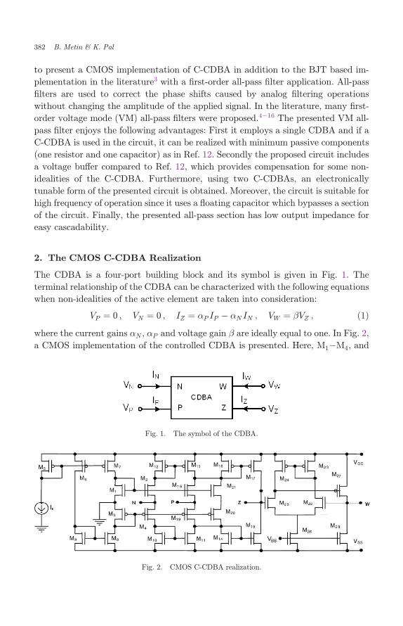
The CDBA is a four-port building block and its symbol is given in Fig. 1. The
terminal relationship of the CDBA can be characterized with the following equations
when non-idealities of the active element are taken into consideration:
VP ¼ 0 ; VN ¼ 0 ; IZ ¼ �P IP � �N IN ; VW ¼ �VZ ; ð1Þwhere the current gains �N , �P and voltage gain � are ideally equal to one. In Fig. 2,
a CMOS implementation of the controlled CDBA is presented. Here, M1�M4, and
Fig. 1. The symbol of the CDBA.
Fig. 2. CMOS C-CDBA realization.
382 B. Metin & K. Pal
M18 and M19 realize a mixed translinear loop derived from Ref. 17 by ¯xing for both
N and P terminals at the ground potential.M5�M10 andM12 provides biasing for the
mixed translinear loops. The M11, M13�M19 and M20�M21 form a current di®eren-
cing circuit at the Z terminal for the currents °owing in to the N and P terminals.
The transistors M22�M28 provide a voltage bu®er between the Z and W terminals.
RN and RP values depend on operation region of the MOS transistors M2, M4, M18
and M19. If MOS transistors operate in weak inversion (subthreshold region) with
small bias currents or control currents (IC), the model equations of the MOS tran-
sistors are exponential. The current equation can be given as follows17:
ID ¼ W
LID0e
qVGSnkT ð1� e�
qVDSkT Þ ; ð2Þ
where n is typically 1.2�1.5 and ID0 is the drain current at VDS ¼ 0 for W=L ¼ 1. If
the exponential term with VDS in Eq. (2) ignored, the parasitic resistances RN and
RP in series to the N and P terminals can be calculated as follows17:
RN ¼ RP ¼ VT
2IC; ð3Þ
where VT � kT=q � 26mV at 27�C is the thermal voltage. For adequately high
current values of IC (i.e., in strong inversion), and if the MOS transistors operate in
saturation region, RN and RP resistors can be calculated as follows:
RN ¼ 1
gm2 þ gm4
; RP ¼ 1
gm18 þ gm19
; ð4Þ
where gm4, gm18, and gm19 are the transconductances of M2, M4, M18, and M19,
respectively. They are calculated as follows: gmi ¼ffiffiffiffiffiffiffiffiffiffiffiffi2�iIC
p, ði ¼ 2; 4; 18; 19Þ.
3. Simulation Results: Characteristics of the CMOS C-CDBA
To verify the theoretical analyses, we simulated the proposed circuit using presented
CMOS C-CDBA in Fig. 2, using the SPICE circuit simulation program. The 0.35�m
level 3TSMCSPICEparameters inTable 1 are used in the simulations.TheDC supply
voltages are � 2.5V and biasing voltage VBB is �1.0V. The aspect ratio of the tran-
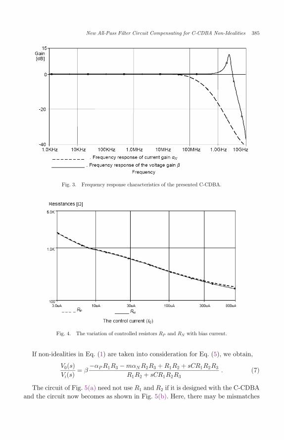
sistors is given in Table 2. Figure 3 shows frequency response characteristics of the
C-CDBA's current and voltage gains. The non-ideal current gains of the C-CDBA at
su±ciently low frequencies are �P ¼ 0:963 and �N ¼ 0:960. Also, the variation of the
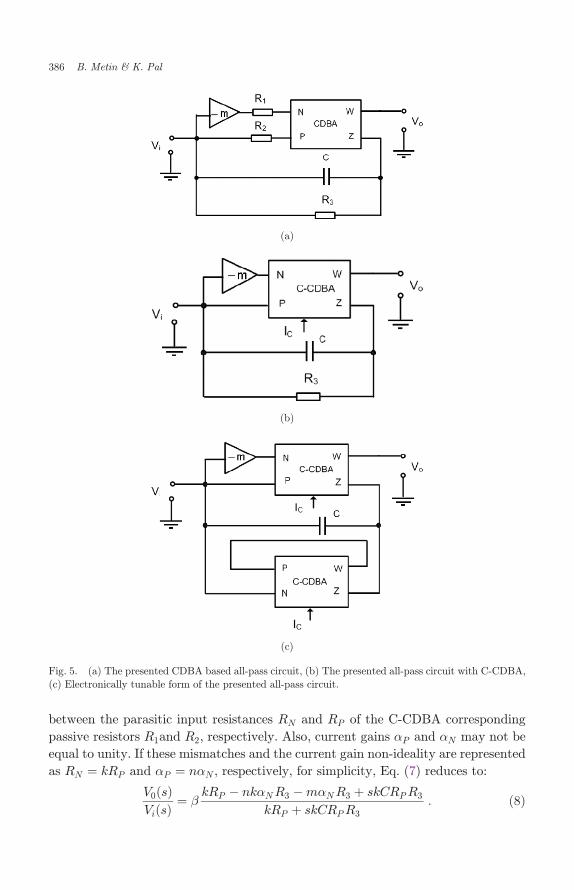
RP andRN of the presented C-CDBA with control current in DC analysis is shown in
Fig. 4. It shows a wide variation and good matching between the RP and RN .
4. Application Example: A Voltage Mode All-Pass Filter
Compensating for C-CDBA Non-Idealities
A C-CDBA may have some deviations in the gain parameters along with the mis-
matches between the parasitic input-resistors RP and RN due to the IC realization.
New All-Pass Filter Circuit Compensating for C-CDBA Non-Idealities 383
Since these cannot be corrected after production and cause undesired e®ects, there is
a need for compensation in C-CDBA based circuits. For this purpose, a new all-pass
¯lter circuit is proposed in this study. The voltage bu®er in the proposed circuit can
be used to compensate for some C-CDBA non-idealities. The presented all-pass ¯lter
is shown in Fig. 5 in various con¯gurations. The transfer function of the circuit in
Fig. 5(a) can be given as follows:
V0ðsÞViðsÞ
¼ �R1R3 �mR2R3 þR1R2 þ sCR1R2R3
R1R2 þ sCR1R2R3
: ð5Þ
Assuming R1 ¼ R2 ¼ R3 ¼ R and m ¼ 1 the transfer function of the circuit
reduces to,
V0ðsÞViðsÞ
¼ �1þ sCR
1þ sCR: ð6Þ
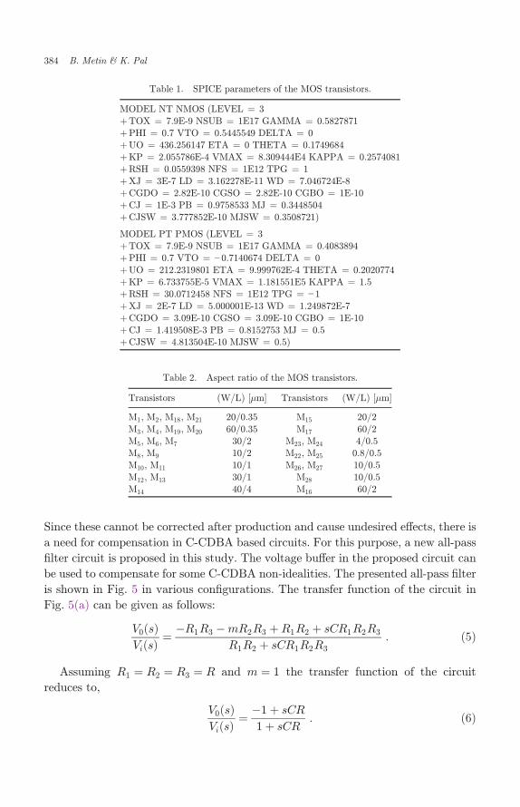
Table 1. SPICE parameters of the MOS transistors.
MODEL NT NMOS (LEVEL ¼ 3
þTOX ¼ 7.9E-9 NSUB ¼ 1E17 GAMMA ¼ 0.5827871
þPHI ¼ 0.7 VTO ¼ 0.5445549 DELTA ¼ 0þUO ¼ 436.256147 ETA ¼ 0 THETA ¼ 0.1749684
þKP ¼ 2.055786E-4 VMAX ¼ 8.309444E4 KAPPA ¼ 0.2574081
þRSH ¼ 0.0559398 NFS ¼ 1E12 TPG ¼ 1
þXJ ¼ 3E-7 LD ¼ 3.162278E-11 WD ¼ 7.046724E-8þCGDO ¼ 2.82E-10 CGSO ¼ 2.82E-10 CGBO ¼ 1E-10
þCJ ¼ 1E-3 PB ¼ 0.9758533 MJ ¼ 0.3448504
þCJSW ¼ 3.777852E-10 MJSW ¼ 0.3508721)
MODEL PT PMOS (LEVEL ¼ 3
þTOX ¼ 7.9E-9 NSUB ¼ 1E17 GAMMA ¼ 0.4083894þPHI ¼ 0.7 VTO ¼ − 0.7140674 DELTA ¼ 0
þUO ¼ 212.2319801 ETA ¼ 9.999762E-4 THETA ¼ 0.2020774
þKP ¼ 6.733755E-5 VMAX ¼ 1.181551E5 KAPPA ¼ 1.5þRSH ¼ 30.0712458 NFS ¼ 1E12 TPG ¼ − 1þXJ ¼ 2E-7 LD ¼ 5.000001E-13 WD ¼ 1.249872E-7
þCGDO ¼ 3.09E-10 CGSO ¼ 3.09E-10 CGBO ¼ 1E-10
þCJ ¼ 1.419508E-3 PB ¼ 0.8152753 MJ ¼ 0.5þCJSW ¼ 4.813504E-10 MJSW ¼ 0.5)
Table 2. Aspect ratio of the MOS transistors.
Transistors (W/L) [�m] Transistors (W/L) [�m]
M1, M2, M18, M21 20/0.35 M15 20/2
M3, M4, M19, M20 60/0.35 M17 60/2M5, M6, M7 30/2 M23, M24 4/0.5
M8, M9 10/2 M22, M25 0.8/0.5
M10, M11 10/1 M26, M27 10/0.5
M12, M13 30/1 M28 10/0.5M14 40/4 M16 60/2
384 B. Metin & K. Pal
If non-idealities in Eq. (1) are taken into consideration for Eq. (5), we obtain,
V0ðsÞViðsÞ
¼ ���P R1R3 �m�NR2R3 þ R1R2 þ sCR1R2R3
R1R2 þ sCR1R2R3
: ð7Þ
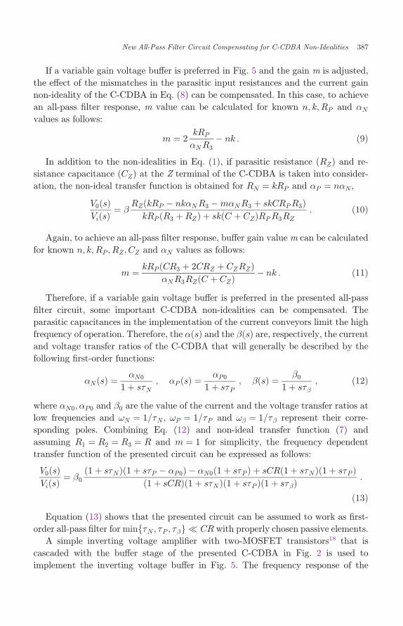
The circuit of Fig. 5(a) need not use R1 and R2 if it is designed with the C-CDBA
and the circuit now becomes as shown in Fig. 5(b). Here, there may be mismatches
Fig. 3. Frequency response characteristics of the presented C-CDBA.
Fig. 4. The variation of controlled resistors RP and RN with bias current.
New All-Pass Filter Circuit Compensating for C-CDBA Non-Idealities 385
between the parasitic input resistances RN and RP of the C-CDBA corresponding
passive resistors R1and R2, respectively. Also, current gains �P and �N may not be
equal to unity. If these mismatches and the current gain non-ideality are represented
as RN ¼ kRP and �P ¼ n�N , respectively, for simplicity, Eq. (7) reduces to:
V0ðsÞViðsÞ
¼ �kRP � nk�NR3 �m�NR3 þ skCRPR3
kRP þ skCRPR3
: ð8Þ
(a)
(b)
(c)
Fig. 5. (a) The presented CDBA based all-pass circuit, (b) The presented all-pass circuit with C-CDBA,
(c) Electronically tunable form of the presented all-pass circuit.
386 B. Metin & K. Pal
If a variable gain voltage bu®er is preferred in Fig. 5 and the gain m is adjusted,
the e®ect of the mismatches in the parasitic input resistances and the current gain
non-ideality of the C-CDBA in Eq. (8) can be compensated. In this case, to achieve
an all-pass ¯lter response, m value can be calculated for known n; k;RP and �N
values as follows:
m ¼ 2kRP
�NR3
� nk : ð9Þ
In addition to the non-idealities in Eq. (1), if parasitic resistance (RZ) and re-
sistance capacitance (CZ) at the Z terminal of the C-CDBA is taken into consider-
ation, the non-ideal transfer function is obtained for RN ¼ kRP and �P ¼ n�N ,
V0ðsÞViðsÞ
¼ �RZðkRP � nk�NR3 �m�NR3 þ skCRPR3Þ
kRP ðR3 þ RZÞ þ skðC þ CZÞRPR3RZ
: ð10Þ
Again, to achieve an all-pass ¯lter response, bu®er gain value m can be calculated
for known n; k;RP ;RZ ;CZ and �N values as follows:
m ¼ kRP ðCR3 þ 2CRZ þ CZRZÞ�NR3RZðC þ CZÞ
� nk : ð11Þ
Therefore, if a variable gain voltage bu®er is preferred in the presented all-pass
¯lter circuit, some important C-CDBA non-idealities can be compensated. The
parasitic capacitances in the implementation of the current conveyors limit the high
frequency of operation. Therefore, the �ðsÞ and the �ðsÞ are, respectively, the currentand voltage transfer ratios of the C-CDBA that will generally be described by the
following ¯rst-order functions:
�NðsÞ ¼�N0
1þ s�N; �P ðsÞ ¼
�P0
1þ s�P; �ðsÞ ¼ �0
1þ s��; ð12Þ
where �N0; �P0 and �0 are the value of the current and the voltage transfer ratios at
low frequencies and !N ¼ 1=�N , !P ¼ 1=�P and !� ¼ 1=�� represent their corre-
sponding poles. Combining Eq. (12) and non-ideal transfer function (7) and
assuming R1 ¼ R2 ¼ R3 ¼ R and m ¼ 1 for simplicity, the frequency dependent
transfer function of the presented circuit can be expressed as follows:
V0ðsÞViðsÞ
¼ �0
ð1þ s�NÞð1þ s�P � �P0Þ � �N0ð1þ s�P Þ þ sCRð1þ s�NÞð1þ s�P Þð1þ sCRÞð1þ s�NÞð1þ s�P Þð1þ s��Þ
:
ð13ÞEquation (13) shows that the presented circuit can be assumed to work as ¯rst-
order all-pass ¯lter forminf�N ; �P ; ��g � CR with properly chosen passive elements.
A simple inverting voltage ampli¯er with two-MOSFET transistors18 that is
cascaded with the bu®er stage of the presented C-CDBA in Fig. 2 is used to
implement the inverting voltage bu®er in Fig. 5. The frequency response of the
New All-Pass Filter Circuit Compensating for C-CDBA Non-Idealities 387
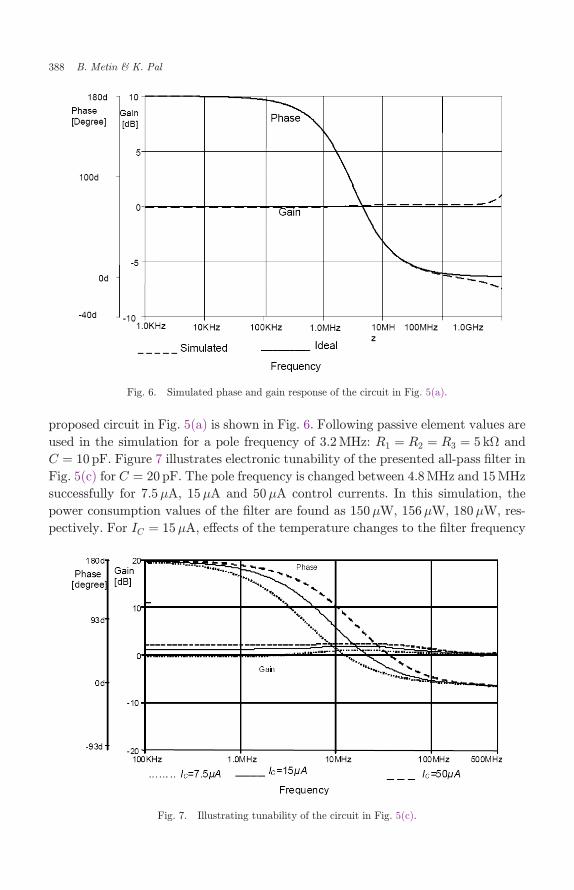
proposed circuit in Fig. 5(a) is shown in Fig. 6. Following passive element values are
used in the simulation for a pole frequency of 3.2MHz: R1 ¼ R2 ¼ R3 ¼ 5 k� and
C ¼ 10 pF. Figure 7 illustrates electronic tunability of the presented all-pass ¯lter in
Fig. 5(c) for C ¼ 20 pF. The pole frequency is changed between 4.8MHz and 15MHz
successfully for 7.5�A, 15�A and 50�A control currents. In this simulation, the
power consumption values of the ¯lter are found as 150�W, 156�W, 180�W, res-
pectively. For IC ¼ 15�A, e®ects of the temperature changes to the ¯lter frequency
Fig. 6. Simulated phase and gain response of the circuit in Fig. 5(a).
Fig. 7. Illustrating tunability of the circuit in Fig. 5(c).
388 B. Metin & K. Pal
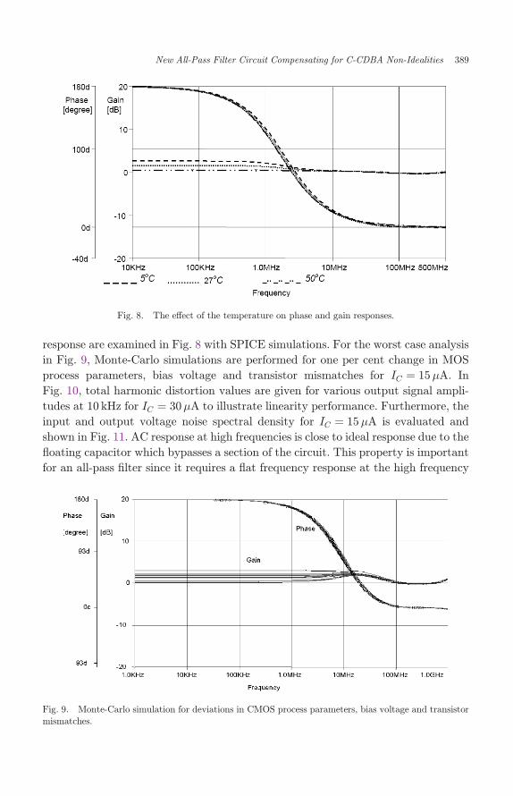
response are examined in Fig. 8 with SPICE simulations. For the worst case analysis
in Fig. 9, Monte-Carlo simulations are performed for one per cent change in MOS
process parameters, bias voltage and transistor mismatches for IC ¼ 15�A. In
Fig. 10, total harmonic distortion values are given for various output signal ampli-
tudes at 10 kHz for IC ¼ 30�A to illustrate linearity performance. Furthermore, the
input and output voltage noise spectral density for IC ¼ 15�A is evaluated and
shown in Fig. 11. AC response at high frequencies is close to ideal response due to the
°oating capacitor which bypasses a section of the circuit. This property is important
for an all-pass ¯lter since it requires a °at frequency response at the high frequency
Fig. 8. The e®ect of the temperature on phase and gain responses.
Fig. 9. Monte-Carlo simulation for deviations in CMOS process parameters, bias voltage and transistormismatches.
New All-Pass Filter Circuit Compensating for C-CDBA Non-Idealities 389
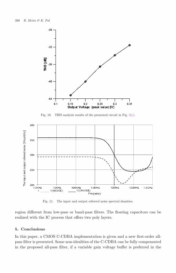
region di®erent from low-pass or band-pass ¯lters. The °oating capacitors can be
realized with the IC process that o®ers two poly layers.
5. Conclusions
In this paper, a CMOS C-CDBA implementation is given and a new ¯rst-order all-
pass ¯lter is presented. Some non-idealities of the C-CDBA can be fully compensated
in the proposed all-pass ¯lter, if a variable gain voltage bu®er is preferred in the
Fig. 10. THD analysis results of the presented circuit in Fig. 5(c).
Fig. 11. The input and output refereed noise spectral densities.
390 B. Metin & K. Pal
circuit. Electronically tunable form of the proposed all-pass ¯lter is given using the
presented C-CDBA. Simulations are performed to verify the theory.
Acknowledgments
This work was supported by Bogazici University Research Fund with the project
code 08N304.
References
1. C. Acar and S. Ozoguz, A new versatile building block: Current di®erencing bu®eredampli¯er suitable for analog signal processing ¯lters,Microeletron. J. 30 (1999) 157�160.
2. A. Fabre, O. Saaid, F. Wiest and C. Boucheron, High frequency applications based on anew current controlled conveyor, IEEE Trans. Circuits Syst. I 43 (1996) 82�91.
3. S. Maheshwari and I. A. Khan, Current controlled current di®erencing bu®ered ampli¯er:Implementation and applications, Active and Passive Electronic Components 4 (2004)219�227.
4. N. Pandey and S. K. Paul, All-pass ¯lters based on CCII- and CCCII-, Int. J. Electron. 91(2004) 485�489.
5. J. W. Horng, Current conveyors based all-pass ¯lters and quadrature oscillatorsemploying grounded capacitors and resistors, Comput. Electr. Eng. 31 (2005) 81�92.
6. J. W. Horng, C. L. Hou, C. M. Chang, I. C. Shiu andW. Y. Chiu, First-order all-pass ¯lterand sinusoidal oscillators using DDCCs, Int. J. Electron. 93 (2006) 457�466.
7. B. Metin, A. Toker, H. Terzioglu and O. Cicekoglu, A new all-pass section for high-performance signal processing with a single CCII-, Frequenz 57 (2003) 241�243.
8. I. A. Khan and S. Maheshwari, Simple ¯rst order all-pass section using a single CCII,Int. J. Electron. 87 (2000) 303�306.
9. A. Toker, S. Ozcan, H. Kuntman and O. Cicekoglu, Supplementary all-pass sections withreduced number of passive elements using a single current conveyor, Int. J. Electron. 88(2001) 969�976.
10. R. I. Salawu, Realization of an all-pass transfer function using the second generationcurrent conveyor, Proc. IEEE 68 (1980) 183�184.
11. S. Maheshwari and I. A. Khan, Novel ¯rst order all-pass sections using a single CCIII,Int. J. Electron. 88 (2001) 773�778.
12. S. Maheshwari, Voltage-mode all-pass ¯lters including minimum component countcircuits, Active and Passive Electronic Components, doi:10.1155/2007/79159 (2007),Article ID 79159.
13. M. Higashimura and Y. Fukui, Realization of all-pass networks using a current conveyor,Int. J. Electron. 65 (1988) 249�250.
14. S. Minaei and O. Cicekoglu, A resistorless realization of the ¯rst-order all-pass ¯lter,Int. J. Electron. 93 (2006) 177�183.
15. S. Maheshwari, High input impedance VM-APSs with grounded passive elements, IETCircuits Dev. Syst. 1 (2007) 72�78.
16. S. Maheshwari, High input impedance voltage-mode ¯rst-order all-pass sections, Int. J.Circ. Theor. Appl. 36 (2008) 511�522.
17. E. Altuntas and A. Toker, Realization of voltage and current mode KHN biquads usingCCCIIs, AEU 56 (2002) 45�49.
18. A. S. Sedra and K. C. Smith, Microelectronic Circuits, 5th ed. (Oxford University Press,Oxford, 2003).
New All-Pass Filter Circuit Compensating for C-CDBA Non-Idealities 391

![Active low pass filter design[1]](https://static.fdokumen.com/doc/165x107/631aaeddd43f4e1763048eee/active-low-pass-filter-design1.jpg)