Nanolayered Lightweight Flexible Shields With Multidirectional Optical Transparency
10
602 IEEE TRANSACTIONS ON ELECTROMAGNETIC COMPATIBILITY, VOL. 47, NO. 3, AUGUST 2005 Nanolayered Lightweight Flexible Shields With Multidirectional Optical Transparency Maria Sabrina Sarto, Senior Member, IEEE, Roberto Li Voti, Francesca Sarto, and Maria Cristina Larciprete Abstract—New nanolayered coatings are designed and deposited on flexible plastic substrate having the thickness of 100 µm, in or- der to realize lightweight ultrathin transparent shielding foils. The structure of the coating is optimized considering three figures of merit: the average transmittance in the visible range for normal incidence, the normalized average transmittance for oblique inci- dence at 550 nm, and the transmittance quality factor. The nan- otechnology exploited for the deposition of the transparent met- als is the dual ion beam sputtering. Tests of durability, optical transmission, and shielding effectiveness demonstrate that the film has a high adhesion under mechanical solicitation, high resistance against aging, peak transmittance in the visible range higher than 70%, omnidirectional properties in the range 0 ◦ –60 ◦ , and shielding effectiveness of 40 dB up to 6 GHz. Index Terms—Nanotechnology, optical coating, shielding, thin film. I. INTRODUCTION T HE USE of plastics is rapidly spreading in today’s elec- tronic market, which is pushing manufacturers to provide products that are smaller, more efficient, and have higher per- formance than ever before. Plastics allow highly cosmetic hous- ings, which are also lightweight and cost-effective. A crucial aspect that should be considered in the design of housing for electronic devices is the radiated emission and susceptibility of the equipment against radio frequency (RF) electromagnetic (EM) fields. Numerous studies and technological solutions have been proposed in order to improve the shielding performance of lightweight plastics [1]–[5]. However, a critical point is the screening of video display or other functional apertures, which must be characterized by high transparency in the visible range in order to allow optical inspection. Since 2003, a two year research project, supported by the Italian Minister of Scientific and Technological Research, has been coordinated by the Electromagnetic Compatibility group of the University of Rome “La Sapienza,” and carried out in collaboration with the Physics Optics group of the same Uni- versity and the Thin Film Laboratory of the ENEA Research Manuscript received January 14, 2004; revised January 27, 2005. This paper has been performed within the research project of relevant interest, supported by the Italian Minister of Scientific Research for the years 2003–2004, en- titled “Nanotechnology of new electromagnetic shields transparent at optical frequencies.” M. S. Sarto is with the Department of Electrical Engineering, Univer- sity of Rome “La Sapienza”, 00184 Rome, Italy (e-mail: mariasabrinasarto@ uniroma1.it). R. Li Voti and M. C. Larciprete are with INFM at the Department of Ener- getica, University of Rome “La Sapienza”, 00161 Rome, Italy. F. Sarto is with the Advanced Physics Technologies Unit—ENEA, 00060, Rome, Italy. Digital Object Identifier 10.1109/TEMC.2005.853214 Centre of Rome. The project is finalized to the design and re- alization of innovative shields, made of transparent metals, and characterized by high transparency in the visible range. Considerable work has been carried out in the optical com- munity on the development of transparent conductive coatings, specially for solar radiation control applications. The use of such coatings for EMI shielding requires lower sheet resis- tance values to be satisfied and the electrical bonding critical issue to be addressed. Recently, the theory of photonic crys- tals [6]–[10] has been applied to the study of metallo-dielectric coatings [11], [12], the so called “transparent metals,” in or- der to better understand and predict accurately their optical performance. Transparent metals are monodimensional (1-D) photonic band gap (PBG) structures characterized by passband properties in the optical range [11], [12]. The ability of transparent metals to shield EM fields at ra- dio frequency, i.e., from a few megahertz up to 1.5 GHz, was demonstrated in [13]–[16]. The state of art for transparent met- als is discussed in detail in [15]. Transparent metals with either flat- or resonant-like transmission spectra have been designed and realized. The use of different target materials such as zinc oxide and titanium oxide has been considered in order to exploit nonlinear optical properties [17] or to improve transmittance in the visible range [15]. The crucial aspect of electrical bonding has been also investigated [14]. The nanotechnology exploited for the deposition of such films on either glass or plastic substrate is the dual ion beam sputtering (DIBS), which allows high control of the coating thickness and masking. The results obtained demonstrated that the peak trans- missivity of the realized samples for normal incidence reaches nearly 70% in the visible range, and the shielding effectiveness (SE) from 30 MHz to 1.5 GHz is greater than 40 dB. The scope of this paper is to present the latest results of our two year research project. The major advance described in this paper, with respect to the previous work described in [13]–[16], concerns the following three aspects. First, the feasibility of the transparent metal deposition on plastic flexible substrate is in- vestigated; this is of particular interest in the exploitation of the new material to screen nonplanar surfaces such as video dis- plays, sensor caps, etc. Second, the optical transmittance of the transparent metal in the case of oblique incidence is optimized; this is needed if the coating is applied on nonplanar substrate. Third, the shielding performance of the transparent metal is as- sessed experimentally and maximized in the frequency range up to 6 GHz. New nanolayered coatings are designed and deposited on flexible plastic substrate having the thickness of 100 µm, in order to realize lightweight ultrathin transparent shielding foil, 0018-9375/$20.00 © 2005 IEEE
-
Upload
independent -
Category
Documents
-
view
0 -
download
0
Transcript of Nanolayered Lightweight Flexible Shields With Multidirectional Optical Transparency
602 IEEE TRANSACTIONS ON ELECTROMAGNETIC COMPATIBILITY, VOL. 47, NO. 3, AUGUST 2005
Nanolayered Lightweight Flexible Shields WithMultidirectional Optical Transparency
Maria Sabrina Sarto, Senior Member, IEEE, Roberto Li Voti, Francesca Sarto, and Maria Cristina Larciprete
Abstract—New nanolayered coatings are designed and depositedon flexible plastic substrate having the thickness of 100 µm, in or-der to realize lightweight ultrathin transparent shielding foils. Thestructure of the coating is optimized considering three figures ofmerit: the average transmittance in the visible range for normalincidence, the normalized average transmittance for oblique inci-dence at 550 nm, and the transmittance quality factor. The nan-otechnology exploited for the deposition of the transparent met-als is the dual ion beam sputtering. Tests of durability, opticaltransmission, and shielding effectiveness demonstrate that the filmhas a high adhesion under mechanical solicitation, high resistanceagainst aging, peak transmittance in the visible range higher than70%, omnidirectional properties in the range 0◦–60◦, and shieldingeffectiveness of 40 dB up to 6 GHz.
Index Terms—Nanotechnology, optical coating, shielding, thinfilm.
I. INTRODUCTION
THE USE of plastics is rapidly spreading in today’s elec-tronic market, which is pushing manufacturers to provide
products that are smaller, more efficient, and have higher per-formance than ever before. Plastics allow highly cosmetic hous-ings, which are also lightweight and cost-effective. A crucialaspect that should be considered in the design of housing forelectronic devices is the radiated emission and susceptibilityof the equipment against radio frequency (RF) electromagnetic(EM) fields. Numerous studies and technological solutions havebeen proposed in order to improve the shielding performanceof lightweight plastics [1]–[5]. However, a critical point is thescreening of video display or other functional apertures, whichmust be characterized by high transparency in the visible rangein order to allow optical inspection.
Since 2003, a two year research project, supported by theItalian Minister of Scientific and Technological Research, hasbeen coordinated by the Electromagnetic Compatibility groupof the University of Rome “La Sapienza,” and carried out incollaboration with the Physics Optics group of the same Uni-versity and the Thin Film Laboratory of the ENEA Research
Manuscript received January 14, 2004; revised January 27, 2005. This paperhas been performed within the research project of relevant interest, supportedby the Italian Minister of Scientific Research for the years 2003–2004, en-titled “Nanotechnology of new electromagnetic shields transparent at opticalfrequencies.”
M. S. Sarto is with the Department of Electrical Engineering, Univer-sity of Rome “La Sapienza”, 00184 Rome, Italy (e-mail: [email protected]).
R. Li Voti and M. C. Larciprete are with INFM at the Department of Ener-getica, University of Rome “La Sapienza”, 00161 Rome, Italy.
F. Sarto is with the Advanced Physics Technologies Unit—ENEA, 00060,Rome, Italy.
Digital Object Identifier 10.1109/TEMC.2005.853214
Centre of Rome. The project is finalized to the design and re-alization of innovative shields, made of transparent metals, andcharacterized by high transparency in the visible range.
Considerable work has been carried out in the optical com-munity on the development of transparent conductive coatings,specially for solar radiation control applications. The use ofsuch coatings for EMI shielding requires lower sheet resis-tance values to be satisfied and the electrical bonding criticalissue to be addressed. Recently, the theory of photonic crys-tals [6]–[10] has been applied to the study of metallo-dielectriccoatings [11], [12], the so called “transparent metals,” in or-der to better understand and predict accurately their opticalperformance. Transparent metals are monodimensional (1-D)photonic band gap (PBG) structures characterized by passbandproperties in the optical range [11], [12].
The ability of transparent metals to shield EM fields at ra-dio frequency, i.e., from a few megahertz up to 1.5 GHz, wasdemonstrated in [13]–[16]. The state of art for transparent met-als is discussed in detail in [15]. Transparent metals with eitherflat- or resonant-like transmission spectra have been designedand realized. The use of different target materials such as zincoxide and titanium oxide has been considered in order to exploitnonlinear optical properties [17] or to improve transmittance inthe visible range [15]. The crucial aspect of electrical bondinghas been also investigated [14].
The nanotechnology exploited for the deposition of such filmson either glass or plastic substrate is the dual ion beam sputtering(DIBS), which allows high control of the coating thickness andmasking. The results obtained demonstrated that the peak trans-missivity of the realized samples for normal incidence reachesnearly 70% in the visible range, and the shielding effectiveness(SE) from 30 MHz to 1.5 GHz is greater than 40 dB.
The scope of this paper is to present the latest results of ourtwo year research project. The major advance described in thispaper, with respect to the previous work described in [13]–[16],concerns the following three aspects. First, the feasibility of thetransparent metal deposition on plastic flexible substrate is in-vestigated; this is of particular interest in the exploitation of thenew material to screen nonplanar surfaces such as video dis-plays, sensor caps, etc. Second, the optical transmittance of thetransparent metal in the case of oblique incidence is optimized;this is needed if the coating is applied on nonplanar substrate.Third, the shielding performance of the transparent metal is as-sessed experimentally and maximized in the frequency range upto 6 GHz.
New nanolayered coatings are designed and deposited onflexible plastic substrate having the thickness of 100 µm, inorder to realize lightweight ultrathin transparent shielding foil,
0018-9375/$20.00 © 2005 IEEE
SARTO et al.: NANOLAYERED LIGHTWEIGHT FLEXIBLE SHIELDS WITH MULTIDIRECTIONAL OPTICAL TRANSPARENCY 603
which can be applied directly on the window to be screened bymeans of adhesive glue. The average SE of the material samplein the frequency range from 30 MHz up to 6 GHz should reachthe value of 40 dB.
The new multidirectional transparent metals should also pro-vide maximum optical transmittance higher than 70% for nor-mal incidence in the visible range, and average transmissivity foroblique incidence of 60% with overall silver content of 68 nm.
In the following, we first describe the sample preparation pro-cess. The 1-D PBG structure is optimized in order to achievethe desired design constraints. Three different samples of trans-parent metal are deposited by dual ion beam sputtering.
The results of the mechanical, electromagnetic, and opticaltests performed on the samples are presented and discussed. Theoptical transmittance of the coating, defined as the ratio betweenoutput light intensity and input light intensity, is measured forincidence angle varying from 0◦ up to 60◦. The shielding ef-fectiveness (SE), defined as the ratio between the electric fieldmagnitudes in a point behind the screen, without and with thescreen present, is measured in the frequency range up to 6 GHz,against plane wave and for normal incidence.
II. SAMPLE DESIGN AND PREPARATION
1-D PBG structures are made of material layers whose refrac-tive indexes alternate between a high and a low value. In gen-eral transparent metals are characterized by periodic or pseudo-periodic geometry [6]–[10]: two adjacent layers form a period,which is repeated a number of times. Thanks to the periodicgeometry, the light is allowed to propagate through the wholestructure only at some frequencies, as the electrons in crystals.
The layers thickness is chosen as a fraction of the opticalwavelength to get constructive or destructive interference, andconsequently to obtain high transparency or reflectivity for thedesired wavelengths. In fact, for strictly periodical multilayerstructures, destructive interference gives rise to stop bands inthe transmission spectrum, while constructive interference giverise to Fabry–Perot like resonances. Of course, many parametersplay a fundamental role in the design of a PBG structure: forexample, the thickness and the refractive index of each layerand the number of periods.
The scope of this paper is to design and realize a 1-D PBGstructures that exhibit high optical transmission in the visiblerange, i.e., from 400 to 700 nm, possibly independently of theincidence angle, while maintaining the requirements that guar-antee the optimum shielding performance reported in previousworks [13]–[16].
In the optical coatings community, numerical optimizationprocedures based for instance on the use of genetic algorithmsare widely used to define the optimum multilayer configurationthat satisfies the desired optical requirements. Such approachesdo not, however, provide general information on how variationsof the thickness of the deposited multilayered film can affectthe overall optical performance of the device. For this reason,a sensitivity study of the PBG structures to the layer thicknessis performed in order to extract information useful to orientthe designer in the choice of the most convenient structure for
the specific application of interest. The typical pseudoperiodi-cal symmetrical structure of a metallo-dielectric 1-D photoniccrystal is considered in this sudy as reference geometry.
The shielding effectiveness (SE) of the multilayer in the RFrange is defined as the ratio in decibel between the incident andtransmitted electric (or magnetic) fields. The transmission coef-ficient or transmittance (T) of the structure in the visible rangeis defined as the ratio between the intensities of the transmittedelectric field and the incident one.
A. Requirements
The new transparent metal is constituted by the sequence ofalternating thin layers of conducting and nonconducting mate-rials [13]. Silver (Ag) is used because the location of its plasmaresonance, at about 320 nm, makes it more suitable for trans-mission windows in the visible range than other metals [19].Titanium oxide is chosen as interlayer because it is one of thematerials having the highest refractive index.
The following constraints are required to be considered in thedesign process: First, the new material should provide shieldingeffectiveness higher than 40 dB at radio frequency, i.e., from30 MHz up to 6 GHz. In case of thin films, having thicknessmuch smaller than the skin depth, the shielding phenomenon isdominated by the reflection mechanism at the air-metal inter-face. Moreover, it is demonstrated that the transmission matrixof a nanolayered coating made of alternating layers of metaland dielectric material can be approximated by the transmissionmatrix of a single equivalent film of metal, whose thickness isgiven by the sum of the thickness of the metal layers in thestructure [13]. According to the procedure described in the Ap-pendix, the limit value of SE for frequency approaching zero isexpressed as function of the total silver thickness dAg and of theAg electrical conductivity σAg
SE0 = k + 20 log dAgσAg (1)
in which the constant k assumes the value of 45.51 dB if dAg isin meters (m) and σAg in Siemens-per-meter (S/m). Consideringthat the measured value of σAg for Ag film is 7.75 · 106 S/m [13],it follows from (1) that dAg, should be 68 nm.
Second, the transparent metal is designed to have maximumoptical transmittance T (0, λc) higher than 70% for normal in-cidence (θ = 0) at the central wavelength of the visible range(λc = 550 nm). The responsivity curve of the human eye, shownin Fig. 1, is given by the well known expression [18]:
r(λ) = exp�−2(λ − λ0)2/W 2� (2)
in which λmin = 400 nm, λmax = 700 nm, λ0 = 555 nm, W =83 nm. It is then required that the average transmittance fornormal incidence weighted by the human eye responsivity curve(2), defined by:
Tav(0) =
∫ λmax
λminT (λ; 0)r(λ)dλ∫ λmax
λminr(λ)dλ
(3)
is higher than 60%. The coating should be also characterized byomnidirectional transparency in the visible range. Therefore, itis required that the normalized average transmittance for oblique
604 IEEE TRANSACTIONS ON ELECTROMAGNETIC COMPATIBILITY, VOL. 47, NO. 3, AUGUST 2005
Fig. 1. Normalized responsivity curve of the human eye as function of the freespace wavelength [13].
incidence at λc = 550 nm, defined by
Tobl(λc) =2
πT (λc ; 0)
∫ π/2
0
T (λc ; θ)dθ (4)
is greater than 0.9 and smaller than 1.1. It should be observedthat in general values of Tobl less than one characterize transpar-ent metals with maximum transmittance at 550 nm for normalincidence, whereas values of Tobl greater than one are typical ofcoatings with maximum transmittance at 550 nm for oblique in-cidence. Therefore, the former PBG structures are optimized asoptical filters in the visible range, whereas the passband regionof the latter ones is not centered at 550 nm.
The optical performance of the PBG can be also evaluatedby using the transmittance quality factor QT weighted by thehuman eye responsivity curve, defined by:
QT =
∫ π/2
0 dθ∫ λmax
λminT (λ; θ)r(λ)dλ
π2
∫ λmax
λminr(λ)dλ
(5)
which allows to quantify the optical performance of the coatingas function of both the incidence angle and the frequency.
The optimum choice of d1 and d2 corresponds to the maxi-mum of QT . However, notice that the use of QT only as meritfigure in the design process does not allow to distinguish a prioribetween coatings with passband region centered in the visiblerange (Tobl < 1), or not (Tobl > 1).
The third constraint to be considered in the design processis that the shielding coating should be deposited on a plasticlightweight flexible foil. In addition, the external layer shouldbe nonconducting in order to minimize reflections in the opti-cal range, and at the same time the internal Ag layers shouldbe grounded in order to allow the circulation of the parasiticcurrents, which are responsible for the shielding mechanism.
Finally, it should be considered that the minimum thicknessof the Ag layers must be greater than 10 nm: in fact, experimen-tal studies have demonstrated that for smaller value of the filmthickness, the electrical conductivity of Ag decreases dramati-cally [19].
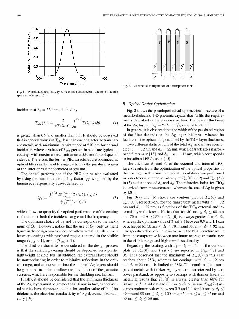
Fig. 2. Schematic configuration of a transparent metal.
B. Optical Design Optimization
Fig. 2 shows the pseudoperiodical symmetrical structure of ametallo-dielectric 1-D photonic crystal that fulfils the require-ments described in the previous section. The overall thicknessof the Ag layers, dAg = 2(d3 + d4), is equal to 68 nm.
In general it is observed that the width of the passband regionof the filter depends on the Ag layer thickness, whereas itslocation in the optical range is tuned by the TiO2 layer thickness.
Two different distributions of the total Ag amount are consid-ered: d3 = 12 nm and d4 = 22 nm, which characterizes narrow-band filters as in [13], and d3 = d4 = 17 nm, which correspondsto broadband PBGs as in [15].
The thickness d1 and d2 of the external and internal TiO2
layers results from the optimization of the optical properties ofthe coating. To this aim, numerical calculations are performedin order to evaluate the sensitivity of Tav(0) in (2) and Tobl(λc)in (3) as functions of d1 and d2. The refractive index for TiO2
is derived from measurements, whereas the one of Ag is givenby [20].
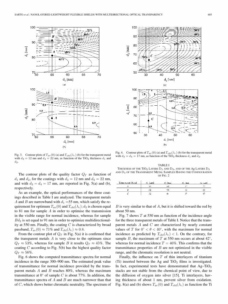
Fig. 3(a) and (b) shows the contour plot of Tav(0) andTobl(λc), respectively, for the transparent metal with d3 = 12nm and d4 = 22 nm, as functions of the TiO2 external and in-ternal layer thickness. Notice that for 50 nm ≤ d1 ≤ 60 nmand 70 nm ≤ d2 ≤ 82 nm Tav(0) is always greater than 60%,whereas the optimum value of Tobl(λc) between 0.9 and 1.1 canbe achieved for 50nm ≤ d1 ≤ 70 nm and 88 nm ≤ d2 ≤ 92 nm.The specific values of d1 and d2 to use in the PBG structure resultfrom the compromise between maximum average transmittancein the visible range and high onmidirectionality.
Regarding the coating with d3 = d4 = 17 nm, the contourplots of Tav(0) and Tobl(λc) are reported in Fig. 4(a) and(b). It is observed that the maximum of Tav(0) in this casereaches about 75%, whereas for coatings with d3 = 12 nmand d4 = 22 nm it is limited to 68%. This confirms that trans-parent metals with thicker Ag layers are characterized by nar-rower passband, as opposite to coatings with thinner layers ofmetal. It results that Tav(0) is always greater than 60% for30 nm ≤ d1 ≤ 44 nm and 60 nm ≤ d2 ≤ 84 nm. Tobl(λc) as-sumes optimum values between 0.9 and 1.1 for 30 nm ≤ d1 ≤40 nm and 86 nm ≤ d2 ≤ 100 nm, or 50 nm ≤ d1 ≤ 65 nm and50 nm ≤ d2 ≤ 58 nm.
SARTO et al.: NANOLAYERED LIGHTWEIGHT FLEXIBLE SHIELDS WITH MULTIDIRECTIONAL OPTICAL TRANSPARENCY 605
Fig. 3. Contour plots of Tav(0) (a) and Tobl(λc ) (b) for the transparent metalwith d3 = 12 nm and d4 = 22 nm, as function of the TiO2 thickness d1 andd2.
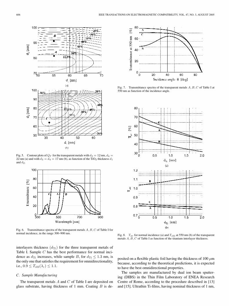
The contour plots of the quality factor QT as function ofd1 and d2, for the coatings with d3 = 12 nm and d4 = 22 nm,and with d3 = d4 = 17 nm, are reported in Fig. 5(a) and (b),respectively.
As an example, the optical performances of the three coat-ings described in Table I are analyzed. The transparent metalsA and B are narrowband with d1 =55 nm, which satisfy the re-quirement for optimum Tav(0) and Tobl(λc); d2 is chosen equalto 81 nm for sample A in order to optimise the transmissionin the visible range for normal incidence, whereas for sampleBd2 is set equal to 91 nm in order to optimize multidirectional-ity at 550 nm. Finally, the coating C is characterized by broadpassband, Tav(0) ≈ 71% and Tobl(λc) ≈ 0.8.
From the contour plot of QT in Fig. 5(a) it is confirmed thatthe transparent metals A is very close to the optimum sinceQT ≈ 53%, whereas for sample B it results QT ≈ 45%. Thecoating C according to Fig. 5(b) has the highest quality factorQT ≈ 56%.
Fig. 6 shows the computed transmittance spectra for normalincidence in the range 300–900 nm. The estimated peak valueof transmittance for normal incidence provided by the trans-parent metals A and B reaches 80%, whereas the maximumtransmittance at 0◦ of sample C is about 77%. In addition, thetransmittance spectra of A and B are much narrower than thatof C, which shows better chromatic neutrality. The spectrum of
Fig. 4. Contour plots of Tav(0) (a) and Tobl(λc ) (b) for the transparent metalwith d3 = d4 = 17 nm, as function of the TiO2 thickness d1 and d2.
TABLE ITHICKNESS OF THE TiO2 LAYERS D1 AND D2, AND OF THE Ag LAYERS D3
AND D4 OF THE TRANSPARENT METAL SAMPLES HAVING THE CONFIGURATION
OF FIG. 2
B is very similar to that of A, but it is shifted toward the red byabout 50 nm.
Fig. 7 shows T at 550 nm as function of the incidence anglefor the three transparent metals of Table I. Notice that the trans-parent metals A and C are characterized by nearly constantvalues of T for 0◦ < θ < 40◦, with the maximum for normalincidence as predicted by Tobl(λc) < 1. On the contrary, forsample B, the maximum of T at 550 nm occurs at about 42◦,whereas for normal incidence T = 46%. This confirms that thetransmittance properties of B are not optimized in the visiblerange, and the chromatic resolution is not neutral.
Finally, the influence on T of thin interlayers of titanium(Ti) inserted between the Ag and TiO2 films is investigated.In fact, experimental tests have demonstrated that Ag–TiO2
stacks are not stable from the chemical point of view, due tothe diffusion of oxygen into silver [15]. Ti interlayers, hav-ing thickness of about 1 nm, prevent silver from oxidation.Fig. 8(a) and (b) shows Tav(0) and Tobl(λc) as function the Ti
606 IEEE TRANSACTIONS ON ELECTROMAGNETIC COMPATIBILITY, VOL. 47, NO. 3, AUGUST 2005
Fig. 5. Contour plots of QT for the transparent metals with d3 = 12 nm, d4 =22 nm (a) and with d3 = d4 = 17 nm (b), as function of the TiO2 thickness d1
and d2.
Fig. 6. Transmittance spectra of the transparent metals A, B, C of Table I fornormal incidence, in the range 300–900 nm.
interlayers thickness (dTi) for the three transparent metals ofTable I. Sample C has the best performance for normal inci-dence as dTi increases, while sample B, for dTi ≤ 1.3 nm, isthe only one that satisfies the requirement for omnidirectionality,i.e., 0.9 ≤ Tobl(λc) ≤ 1.1.
C. Sample Manufacturing
The transparent metals A and C of Table I are deposited onglass substrate, having thickness of 1 mm. Coating B is de-
Fig. 7. Transmittance spectra of the transparent metals A, B, C of Table I at550 nm as function of the incidence angle.
Fig. 8. Tav for normal incidence (a) and Tobl at 550 nm (b) of the transparentmetals A, B, C of Table I as function of the titanium interlayer thickness.
posited on a flexible plastic foil having the thickness of 100 µmbecause, according to the theoretical predictions, it is expectedto have the best omnidirectional properties.
The samples are manufactured by dual ion beam sputter-ing (DIBS) in the Thin Film Laboratory of ENEA ResearchCentre of Rome, according to the procedure described in [13]and [15]. Ultrathin Ti-films, having nominal thickness of 1 nm,
SARTO et al.: NANOLAYERED LIGHTWEIGHT FLEXIBLE SHIELDS WITH MULTIDIRECTIONAL OPTICAL TRANSPARENCY 607
are inserted as interlayer between the Ag and TiO2 ones in orderto prevent oxygen migration from the TiO2 film to the Ag ones.
At first, the deposition rate of each material is derived fromthe measurement of the film thickness divided by the deposi-tion time. The film thickness is measured by stylus profilometryhaving typical precision of 1 nm. Regarding the TiO2 and Agcoatings, the fabrication errors in the layer thickness, includingprocess reproducibility, are within ±2 nm for the dielectric lay-ers and ±1 nm for the silver ones. Regarding the ultrathin Tiinterlayers, the thickness of the deposited films is estimated byfitting the measured optical transmittance curves of the samplesrealized. Our results show that the nominal thickness of 1 nm isreduced in practice to about 0.5 nm due to the oxygen diffusionfrom the Ti film when it is exposed to the oxygen gas during theadjacent TiO2 layer deposition [15].
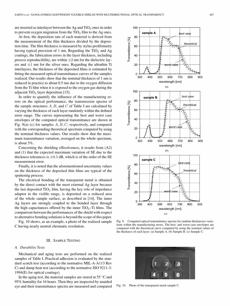
In order to quantify the influence of the manufacturing er-rors on the optical performance, the transmission spectra ofthe sample structures A,B, and C of Table I are calculated byvarying the thickness of each layer randomly within the definederror range. The curves representing the best and worst caseenvelopes of the computed optical transmittance are shown inFig. 9(a)–(c) for samples A,B,C, respectively, and comparedwith the corresponding theoretical spectrum computed by usingthe nominal thickness values. Our results show that the maxi-mum transmittance variation, averaged on the whole spectrum,is about 5%.
Concerning the shielding effectiveness, it results from (A2)and (1) that the expected maximum variation of SE due to thethickness tolerances is ±0.5 dB, which is of the order of the SEmeasurement error.
Finally, it is noted that the aforementioned uncertainty valueson the thickness of the deposited thin films are typical of thesputtering process.
The electrical bonding of the transparent metal is obtainedby the direct contact with the most external Ag layer becausethe last deposited TiO2 film, having the key role of impedanceadaptor in the visible range, is deposited on a reduced areaof the whole sample surface, as described in [14]. The innerAg layers are strongly coupled to the bonded layer throughthe high capacitances offered by the inner TiO2–Ti films. Thecomparison between the performances of the shield with respectto alternative bonding solutions is beyond the scope of this paper.
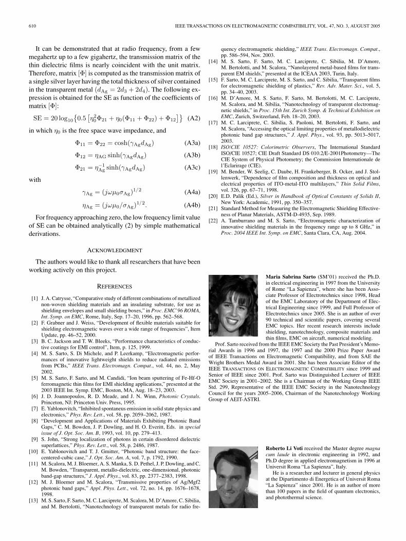
Fig. 10 shows, as an example, a photo of the realized sampleC having nearly neutral chromatic resolution.
III. SAMPLE TESTING
A. Durability Tests
Mechanical and aging tests are performed on the realizedsamples of Table I. Practical adhesion is evaluated by the stan-dard scotch test (according to the normative MIL-A-A113 RevC) and damp heat test (according to the normative ISO 9211-3:1994(E) for optical coatings).
In the aging test, the material samples are stored at 55 ◦C and95% humidity for 16 hours. Then they are inspected by unaidedeye and their transmittance spectra are measured and compared
Fig. 9. Computed optical transmittance spectra for random thicknesses varia-tions within the manufacturing errors. The best- and worst-case envelopes arecompared with the theoretical curve computed by using the nominal values ofthe thickness of each layer. (a) Sample A. (b) Sample B. (c) Sample C.
Fig. 10. Photo of the transparent metal sample C.
608 IEEE TRANSACTIONS ON ELECTROMAGNETIC COMPATIBILITY, VOL. 47, NO. 3, AUGUST 2005
with the ones recorded before the aging test. Our results showthat the film properties are not altered after aging.
In order to assess the adhesion properties of the film on theflexible substrate, sample B is bent 180◦ around metal cylindersof different diameters. The adhesive tape (certified accordingto the MIL A-A113 Rev. C: normative for coating adhesion) isapplied on the bend area of the film and removed with a quickpull. No film detachment is observed for cylinder diametersdown to 1 mm.
B. Optical Transmittance
Specular transmittance spectra at normal and oblique inci-dence are recorded in the visible-NIR (near infra-red) rangeby standard spectrophotometric technique (Lambda 19, doublebeam spectrophotometer by Perkin-Elmer).
In the case of oblique incidence, the sample is mounted ona routable sample holder, able to be tilted with respect to thebeam direction from 0◦ to 60◦. A second sample holder is placedinside the sample compartment, in symmetric position with re-spect to the first one, and rotates in the opposite direction bymeans of three rotating wheels. A bare substrate with the samethickness of the sample is mounted on this second sample holderto prevent lateral displacement of the beam on the detector. Themeasured transmittance spectrum is multiplied to the one of thebare substrate, in order to obtain absolute values. All spectra arerecorded by selecting the TE and TM polarization by mean ofa rotating polarizer placed between the sample and the detec-tor. The average polarization spectra are then obtained by thearithmetic mean of the TE and TM recorded ones.
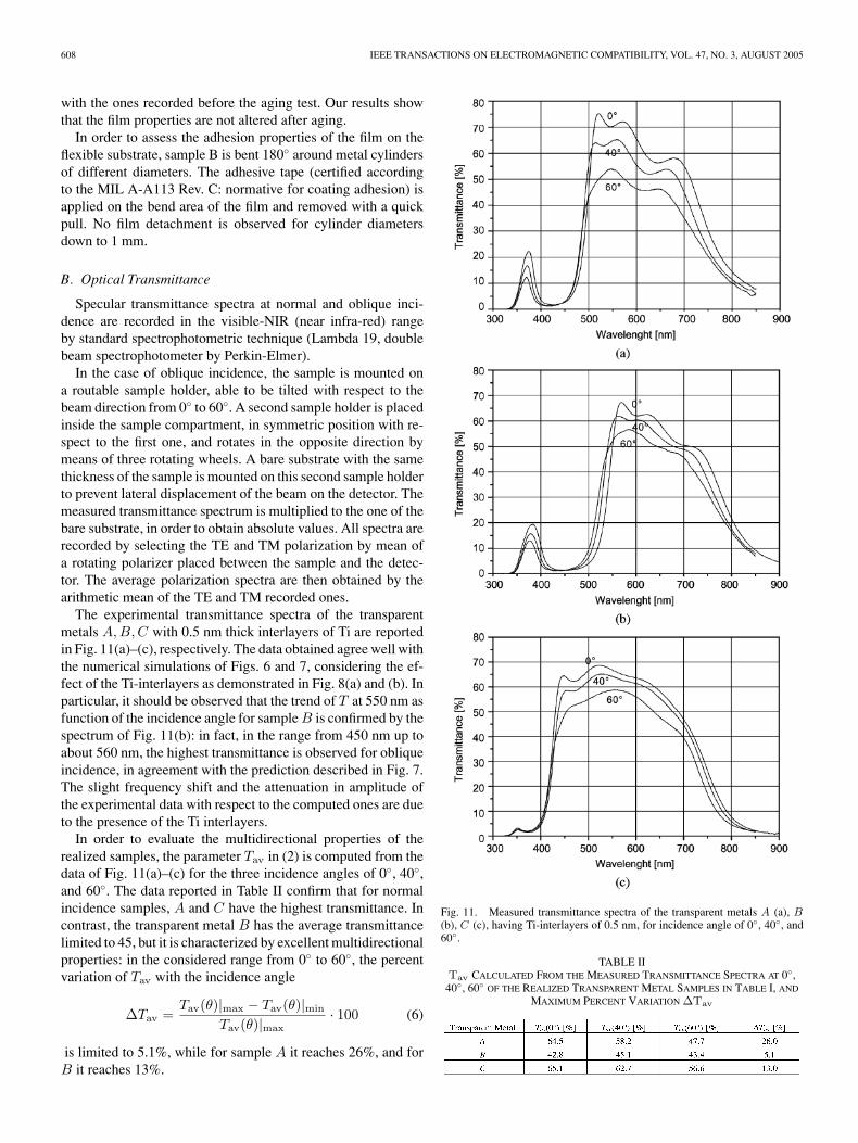
The experimental transmittance spectra of the transparentmetals A,B,C with 0.5 nm thick interlayers of Ti are reportedin Fig. 11(a)–(c), respectively. The data obtained agree well withthe numerical simulations of Figs. 6 and 7, considering the ef-fect of the Ti-interlayers as demonstrated in Fig. 8(a) and (b). Inparticular, it should be observed that the trend of T at 550 nm asfunction of the incidence angle for sample B is confirmed by thespectrum of Fig. 11(b): in fact, in the range from 450 nm up toabout 560 nm, the highest transmittance is observed for obliqueincidence, in agreement with the prediction described in Fig. 7.The slight frequency shift and the attenuation in amplitude ofthe experimental data with respect to the computed ones are dueto the presence of the Ti interlayers.
In order to evaluate the multidirectional properties of therealized samples, the parameter Tav in (2) is computed from thedata of Fig. 11(a)–(c) for the three incidence angles of 0◦, 40◦,and 60◦. The data reported in Table II confirm that for normalincidence samples, A and C have the highest transmittance. Incontrast, the transparent metal B has the average transmittancelimited to 45, but it is characterized by excellent multidirectionalproperties: in the considered range from 0◦ to 60◦, the percentvariation of Tav with the incidence angle
∆Tav =Tav(θ)|max − Tav(θ)|min
Tav(θ)|max· 100 (6)
is limited to 5.1%, while for sample A it reaches 26%, and forB it reaches 13%.
Fig. 11. Measured transmittance spectra of the transparent metals A (a), B(b), C (c), having Ti-interlayers of 0.5 nm, for incidence angle of 0◦, 40◦, and60◦.
TABLE IITav CALCULATED FROM THE MEASURED TRANSMITTANCE SPECTRA AT 0◦,
40◦, 60◦ OF THE REALIZED TRANSPARENT METAL SAMPLES IN TABLE I, AND
MAXIMUM PERCENT VARIATION ∆Tav
SARTO et al.: NANOLAYERED LIGHTWEIGHT FLEXIBLE SHIELDS WITH MULTIDIRECTIONAL OPTICAL TRANSPARENCY 609
Fig. 12. Measured and computed shielding effectiveness of sample B .
C. Shielding Effectiveness
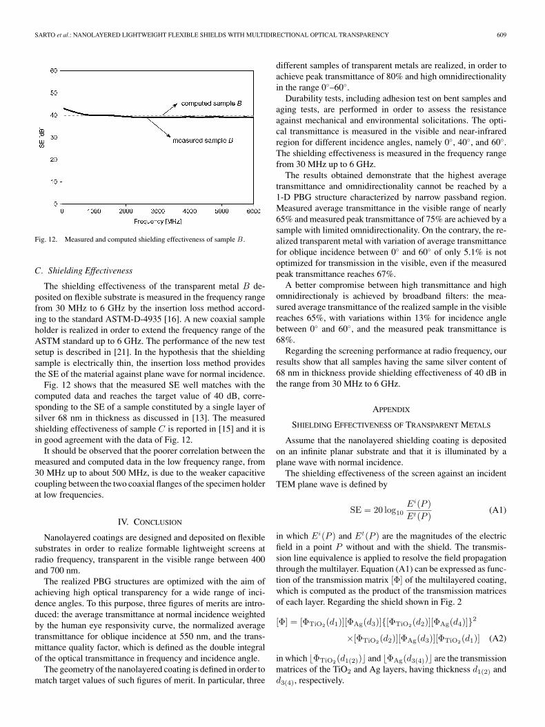
The shielding effectiveness of the transparent metal B de-posited on flexible substrate is measured in the frequency rangefrom 30 MHz to 6 GHz by the insertion loss method accord-ing to the standard ASTM-D-4935 [16]. A new coaxial sampleholder is realized in order to extend the frequency range of theASTM standard up to 6 GHz. The performance of the new testsetup is described in [21]. In the hypothesis that the shieldingsample is electrically thin, the insertion loss method providesthe SE of the material against plane wave for normal incidence.
Fig. 12 shows that the measured SE well matches with thecomputed data and reaches the target value of 40 dB, corre-sponding to the SE of a sample constituted by a single layer ofsilver 68 nm in thickness as discussed in [13]. The measuredshielding effectiveness of sample C is reported in [15] and it isin good agreement with the data of Fig. 12.
It should be observed that the poorer correlation between themeasured and computed data in the low frequency range, from30 MHz up to about 500 MHz, is due to the weaker capacitivecoupling between the two coaxial flanges of the specimen holderat low frequencies.
IV. CONCLUSION
Nanolayered coatings are designed and deposited on flexiblesubstrates in order to realize formable lightweight screens atradio frequency, transparent in the visible range between 400and 700 nm.
The realized PBG structures are optimized with the aim ofachieving high optical transparency for a wide range of inci-dence angles. To this purpose, three figures of merits are intro-duced: the average transmittance at normal incidence weightedby the human eye responsivity curve, the normalized averagetransmittance for oblique incidence at 550 nm, and the trans-mittance quality factor, which is defined as the double integralof the optical transmittance in frequency and incidence angle.
The geometry of the nanolayered coating is defined in order tomatch target values of such figures of merit. In particular, three
different samples of transparent metals are realized, in order toachieve peak transmittance of 80% and high omnidirectionalityin the range 0◦–60◦.
Durability tests, including adhesion test on bent samples andaging tests, are performed in order to assess the resistanceagainst mechanical and environmental solicitations. The opti-cal transmittance is measured in the visible and near-infraredregion for different incidence angles, namely 0◦, 40◦, and 60◦.The shielding effectiveness is measured in the frequency rangefrom 30 MHz up to 6 GHz.
The results obtained demonstrate that the highest averagetransmittance and omnidirectionality cannot be reached by a1-D PBG structure characterized by narrow passband region.Measured average transmittance in the visible range of nearly65% and measured peak transmittance of 75% are achieved by asample with limited omnidirectionality. On the contrary, the re-alized transparent metal with variation of average transmittancefor oblique incidence between 0◦ and 60◦ of only 5.1% is notoptimized for transmission in the visible, even if the measuredpeak transmittance reaches 67%.
A better compromise between high transmittance and highomnidirectionaly is achieved by broadband filters: the mea-sured average transmittance of the realized sample in the visiblereaches 65%, with variations within 13% for incidence anglebetween 0◦ and 60◦, and the measured peak transmittance is68%.
Regarding the screening performance at radio frequency, ourresults show that all samples having the same silver content of68 nm in thickness provide shielding effectiveness of 40 dB inthe range from 30 MHz to 6 GHz.
APPENDIX
SHIELDING EFFECTIVENESS OF TRANSPARENT METALS
Assume that the nanolayered shielding coating is depositedon an infinite planar substrate and that it is illuminated by aplane wave with normal incidence.
The shielding effectiveness of the screen against an incidentTEM plane wave is defined by
SE = 20 log10
Ei(P )Et(P )
(A1)
in which Ei(P ) and Et(P ) are the magnitudes of the electricfield in a point P without and with the shield. The transmis-sion line equivalence is applied to resolve the field propagationthrough the multilayer. Equation (A1) can be expressed as func-tion of the transmission matrix [Φ] of the multilayered coating,which is computed as the product of the transmission matricesof each layer. Regarding the shield shown in Fig. 2
[Φ] = [ΦTiO2(d1)][ΦAg(d3)]{[ΦTiO2(d2)][ΦAg(d4)]}2
×[ΦTiO2(d2)][ΦAg(d3)][ΦTiO2(d1)] (A2)
in which �ΦTiO2(d1(2))� and �ΦAg(d3(4))� are the transmissionmatrices of the TiO2 and Ag layers, having thickness d1(2) andd3(4), respectively.
610 IEEE TRANSACTIONS ON ELECTROMAGNETIC COMPATIBILITY, VOL. 47, NO. 3, AUGUST 2005
It can be demonstrated that at radio frequency, from a fewmegahertz up to a few gigahertz, the transmission matrix of thethin dielectric films is nearly coincident with the unit matrix.Therefore, matrix [Φ] is computed as the transmission matrix ofa single silver layer having the total thickness of silver containedin the transparent metal (dAg = 2d3 + 2d4). The following ex-pression is obtained for the SE as function of the coefficients ofmatrix [Φ]:
SE = 20 log10
{0.5
[η20Φ21 + η0(Φ11 + Φ22) + Φ12
]}(A2)
in which η0 is the free space wave impedance, and
Φ11 = Φ22 = cosh(γAgdAg) (A3a)
Φ12 = ηAG sinh(γAgdAg) (A3b)
Φ21 = η−1Ag sinh(γAgdAg) (A3c)
with
γAg = (jωµ0σAg)1/2 (A4a)
ηAg = (jωµ0/σAg)1/2. (A4b)
For frequency approaching zero, the low frequency limit valueof SE can be obtained analytically (2) by simple mathematicalderivations.
ACKNOWLEDGMENT
The authors would like to thank all researchers that have beenworking actively on this project.
REFERENCES
[1] J. A. Catrysse, “Comparative study of different combinations of metallizednon-woven shielding materials and an insulating substrate, for use asshielding envelopes and small shielding boxes,” in Proc. EMC’96 ROMA,Int. Symp. on EMC, Rome, Italy, Sep. 17–20, 1996, pp. 562–568.
[2] F. Grabner and J. Weiss, “Development of flexible materials suitable forshielding electromagnetic waves over a wide range of frequencies”, ItemUpdate, pp. 46–52, 2000.
[3] B. C. Jackson and T. W. Bleeks, “Performance characteristics of conduc-tive coatings for EMI control”, Item, p. 125, 1999.
[4] M. S. Sarto, S. Di Michele, and P. Leerkamp, “Electromagnetic perfor-mances of innovative lightweight shields to reduce radiated emissionsfrom PCBs,” IEEE Trans. Electromagn. Compat., vol. 44, no. 2, May2002.
[5] M. S. Sarto, F. Sarto, and M. Candidi, “Ion beam sputtering of Fe-Hf-Oferromagnetic thin films for EMI shielding applications,” presented at the2003 IEEE Int. Symp. EMC, Boston, MA, Aug. 18–23, 2003.
[6] J. D. Joannopoulos, R. D. Meade, and J. N. Winn, Photonic Crystals.Princeton, NJ: Princeton Univ. Press, 1995.
[7] E. Yablonovitch, “Inhibited spontaneus emission in solid state physics andelectronics,” Phys. Rev. Lett., vol. 58, pp. 2059–2062, 1987.
[8] “Development and Applications of Materials Exhibiting Photonic BandGaps,” C. M. Bowden, J. P. Dowling, and H. O. Everitt, Eds. in specialissue of J. Opt. Soc. Am. B, 1993, vol. 10, pp. 279–413.
[9] S. John, “Strong localization of photons in certain disordered dielectricsuperlattices,” Phys. Rev. Lett., vol. 58, p. 2486, 1987.
[10] E. Yablonovitch and T. J. Gmitter, “Photonic band structure: the face-centered-cubic case,” J. Opt. Soc. Am. A, vol. 7, p. 1792, 1990.
[11] M. Scalora, M. J. Bloemer, A. S. Manka, S. D. Pethel, J. P. Dowling, and C.M. Bowden, “Transparent, metallo-dielectric, one-dimensional, photonicband-gap structures,” J. Appl. Phys., vol. 83, pp. 2377–2383, 1998.
[12] M. J. Bloemer and M. Scalora, “Transmissive properties of Ag/Mgf2photonic band gaps,” Appl. Phys. Lett., vol. 72, no. 14, pp. 1676–1678,1998.
[13] M. S. Sarto, F. Sarto, M. C. Larciprete, M. Scalora, M. D’Amore, C. Sibilia,and M. Bertolotti, “Nanotechnology of transparent metals for radio fre-
quency electromagnetic shielding,” IEEE Trans. Electromagn. Compat.,pp. 586–594, Nov. 2003.
[14] M. S. Sarto, F. Sarto, M. C. Larciprete, C. Sibilia, M. D’Amore,M. Bertolotti, and M. Scalora, “Nanolayered metal-based films for trans-parent EM shields,” presented at the ICEAA 2003, Turin, Italy.
[15] F. Sarto, M. C. Larciprete, M. S. Sarto, and C. Sibilia, “Transparent filmsfor electromagnetic shielding of plastics,” Rev. Adv. Mater. Sci., vol. 5,pp. 34–40, 2003.
[16] M. D’Amore, M. S. Sarto, F. Sarto, M. Bertolotti, M. C. Larciprete,M. Scalora, and M. Sibilia, “Nanotechnology of transparent electromag-netic shields,” in Proc. 15th Int. Zurich Symp. & Technical Exhibition onEMC, Zurich, Switzerland, Feb. 18–20, 2003.
[17] M. C. Larciprete, C. Sibilia, S. Paoloni, M. Bertolotti, F. Sarto, andM. Scalora, “Accessing the optical limiting properties of metallodielectricphotonic band gap structures,” J. Appl. Phys., vol. 93, pp. 5013–5017,2003.
[18] ISO/CIE 10527: Colorimetric Observers, The International StandardISO/CIE 10527; CIE Draft Standard DS 010.2/E-2001Photometry—TheCIE System of Physical Photometry; the Commission Internationale del’Eclarirage (CIE).
[19] M. Bender, W. Seelig, C. Daube, H. Frankeberger, B. Ocker, and J. Stol-lenwerk, “Dependence of film composition and thickness on optical andelectrical properties of ITO-metal-ITO multilayers,” Thin Solid Films,vol. 326, pp. 67–71, 1998.
[20] E.D. Palik (Ed.), Silver in Handbook of Optical Constants of Solids II,New York: Academic, 1991, pp. 350–357.
[21] Standard Method for Measuring the Electromagnetic Shielding Effective-ness of Planar Materials, ASTM-D-4935, Sep. 1989.
[22] A. Tamburrano and M. S. Sarto, “Electromagnetic characterization ofinnovative shielding materials in the frequency range up to 8 GHz,” inProc. 2004 IEEE Int. Symp. on EMC, Santa Clara, CA, Aug. 2004.
Maria Sabrina Sarto (SM’01) received the Ph.D.in electrical engineering in 1997 from the Universityof Rome “La Sapienza”, where she has been Asso-ciate Professor of Electrotechnics since 1998, Headof the EMC Laboratory of the Department of Elec-trical Engineering since 1999, and Full Professor ofElectrotechnics since 2005. She is an author of over90 technical and scientific papers, covering severalEMC topics. Her recent research interests includeshielding, nanotechnology, composite materials andthin films, EMC on aircraft, numerical modeling.
Prof. Sarto received from the IEEE EMC Society the Past President’s Memo-rial Awards in 1996 and 1997, the 1997 and the 2000 Prize Paper Awardof IEEE Transactions on Electromagnetic Compatibility, and from SAE theWright Brothers Medal Award in 2001. She has been Associate Editor of theIEEE TRANSACTIONS ON ELECTROMAGNETIC COMPATIBILITY since 1999 andSenior of IEEE since 2001. Prof. Sarto was Distinguished Lecturer of IEEEEMC Society in 2001–2002. She is a Chairman of the Working Group IEEEStd. 299, Representative of the IEEE EMC Society in the NanotechnologyCouncil for the years 2005–2006, Chairman of the Nanotechnology WorkingGroup of AEIT-ASTRI.
Roberto Li Voti received the Master degree magnacum laude in electronic engineering in 1992, andPh.D degree in applied electromagnetism in 1996 atUniversit Roma “La Sapienza”, Italy.
He is a researcher and lecturer in general physicsat the Dipartimento di Energetica of Universit Roma“La Sapienza” since 2001. He is an author of morethan 100 papers in the field of quantum electronics,and photothermal science.
SARTO et al.: NANOLAYERED LIGHTWEIGHT FLEXIBLE SHIELDS WITH MULTIDIRECTIONAL OPTICAL TRANSPARENCY 611
Francesca Sarto has the degree in physics.She has been working in ENEA since 1993, as re-
searcher. She has been dealing with PVD techniques,in particular with sputtering and ion assisted tech-niques. Her main interest is the study of the phys-ical mechanisms occurring during the film growth,in order to correlate the film properties to the depo-sition parameters. In particular, her research activityhas been focused on the study and the improvementof the adhesion properties of single layer and mul-tilayer coatings deposited on plastic substrates. She
has carried out her research activity in the framework of national and Europeanprojects, in collaboration with academic and industrial partners, and publishedover 50 technical and scientific papers on this topics on international journalsor in the proceedings of international symposia.
Maria Cristina Larciprete was born in Rome, Italy,in 1974. She received the engineer degree from theUniversity La Sapienza of Rome in 1999 with an ex-perimental thesis on photothermal radiometry withinthe European project Brite-Euram. She pursued thePh.D. degree in the Laboratories of Dipartimentodi Energetica, Engineering faculty, of University ofRome, focusing on the nonlinear optical propertiesof photonic band gap (PBG), metal-dielectric multi-layer structures and optical limiting applications.
Her research interests also include material sci-ence and deposition techniques, i.e. thermal evaporation and sputtering. Atthe moment she is a postdoctoral fellow and is working on fabricationand characterization of polymer microring resonator based integrated opticaldevices.