Nanoelectronic Based Integrated Antennas
71
Nanoelectronic Based Integrated Antennas Johannes A. Russer 1 , Giuseppe Scarpa 1 , Peter Russer 1 , Paolo Lugli 1 , and Wolfgang Porod 2 1 InsAtute for Nanoelectronics, Technische Universität München, Germany 2 Center for Nano Science and Technology, University of Notre Dame, USA
-
Upload
independent -
Category
Documents
-
view
0 -
download
0
Transcript of Nanoelectronic Based Integrated Antennas

Nanoelectronic+Based++
Integrated+Antennas+
Johannes+A.+Russer1,+Giuseppe+Scarpa1,++
Peter+Russer1,+Paolo+Lugli1,+and+Wolfgang+Porod2+
1InsAtute+for+Nanoelectronics,+Technische+Universität+München,+Germany+
2Center+for+Nano+Science+and+Technology,+University+of+Notre+Dame,+USA+

WMF 9: Nanoelectronic Based Integrated Antennas IMS2012, Montreal, June 17-22, 2012 2
Contents
1. Introduction
2. Integrated Antennas:
Realization and modelling (CMOS, Bondwire)
3. Nanoantennas with MOM Tunnel Diodes
4. Carbon-based Nanoantennas
5. Novel fabrication techqniques:
Plasmonic Nanostructures
6. Outlook

WMF 9: Nanoelectronic Based Integrated Antennas IMS2012, Montreal, June 17-22, 2012 3
On-Chip Nanoantennas for
Sensing and Communication
• As the structure size of circuit devices and
components is continuously decreasing the
same will hold for antennas and radiation
elements used in integrated circuits for on-chip
and chip-to-chip communication.
• Following the general scaling trend on-chip
antennas will soon enter the micrometer- and
even the nanometer regime.

WMF 9: Nanoelectronic Based Integrated Antennas IMS2012, Montreal, June 17-22, 2012 4
Introduction
• The rate of signal transmission on or between monolithic integrated
circuits is limited by the cross-talk and the dispersion due to the wired
interconnects.
• An interesting option to overcome the bandwidth limitations is wireless
chip-to-chip and on-chip interconnects via integrated antennas.
• The electromagnetic coupling of antennas may occur via waves
radiated into space and scattered by objects or via surface waves.
WMF 9: Nanoelectronic Based Integrated Antennas IMS2012, Montreal, June 17-22, 2012 5
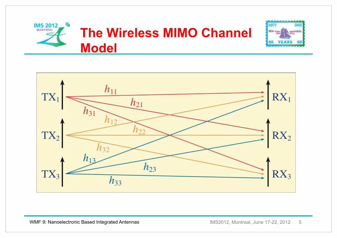
The Wireless MIMO Channel
Model

WMF 9: Nanoelectronic Based Integrated Antennas IMS2012, Montreal, June 17-22, 2012 6
Contents
1. Introduction
2. Integrated Antennas:
Realization and modelling (CMOS, Bondwire)
3. Nanoantennas with MOM Tunnel Diodes
4. Carbon-based Nanoantennas
5. Novel fabrication techqniques:
Plasmonic Nanostructures
6. Outlook

WMF 9: Nanoelectronic Based Integrated Antennas IMS2012, Montreal, June 17-22, 2012 7
On-chip meander antenna
An intrachip wireless interconnect system using meander monopole on-chip
antennas and operating at 22 GHz to 29 GHz is described in M. Sun, et al., “Performance of Intra-Chip wireless interconnect using On-Chip antennas and
UWB radios,’’ IEEE Trans. on Ant. & Prop., vol. 57, no. 9, pp. 2756-2762, 2009.
On-chip UWB radios in that frequency band are discussed there. The on-chip antennas are meander monopoles with 1 mm axial length.

WMF 9: Nanoelectronic Based Integrated Antennas IMS2012, Montreal, June 17-22, 2012 8
Realization I

WMF 9: Nanoelectronic Based Integrated Antennas IMS2012, Montreal, June 17-22, 2012 9
CMOS Integrated Antennas
Schematic drawing of a chip with an integrated antenna
• Instead of dedicating chip area for the antenna the antenna can
make use of the available on-chip metallization.
• This can be obtained by dividing the top metallization layer into
patches and impressing an RF signal across the gap between the
patches.

WMF 9: Nanoelectronic Based Integrated Antennas IMS2012, Montreal, June 17-22, 2012 10
Differential Lines, Connecting the
Digital Circuits Under the Separate
Antenna Patches

WMF 9: Nanoelectronic Based Integrated Antennas IMS2012, Montreal, June 17-22, 2012 11
Chip with Integrated Antenna
Cross section

WMF 9: Nanoelectronic Based Integrated Antennas IMS2012, Montreal, June 17-22, 2012 12
CMOS Integrated Antennas
Main Direction
Minimum Direction

WMF 9: Nanoelectronic Based Integrated Antennas IMS2012, Montreal, June 17-22, 2012 13
Realization II

WMF 9: Nanoelectronic Based Integrated Antennas IMS2012, Montreal, June 17-22, 2012 14
Bond Wires as Antennas
J.A. Russer, F. Mukhtar, S. Wane, D. Bajon, P. Russer, “Broad-Band Modeling of Bond Wire Antenna
Structures” Proc. 2012 German Microwave Conference (GeMIC), Ilmenau, 12-14 March 2012.

WMF 9: Nanoelectronic Based Integrated Antennas IMS2012, Montreal, June 17-22, 2012 15
W.-H. Chen, S. Joo, S. Sayilir, R. Willmot, T.-Y. Choi, D. Kim, J. Lu, D. Peroulis, and B. Jung,
“A 6-Gb/s wireless inter-chip data link using 43-GHz transceivers and bond-wire antennas,”
IEEE Journal of Solid-State Circuits, vol. 44, no. 10, pp. 2711 –2721, oct. 2009.
Transceiver ICs and Bond-
Wire Antennas on a PCB

WMF 9: Nanoelectronic Based Integrated Antennas IMS2012, Montreal, June 17-22, 2012 16
S. Wane, S. Bardy, R. van Heijster, F. Goulet, and P. Gamand, “Design of antenna-on-chip, antenna-
on-package and detectors from RF, microwave to THz frequency range in SiGe-C technology,”
European Microwave Conference (EuMC), Manchester, 2011.
Multi-Chip Module with Bondwire
Antenna Array.

WMF 9: Nanoelectronic Based Integrated Antennas IMS2012, Montreal, June 17-22, 2012 17
CMOS and CML Power Detectors
Using SiGe-C Technology
S. Wane, S. Bardy, R. van Heijster, F. Goulet, and P. Gamand, “Design of antenna-on-chip, antenna-
on-package and detectors from RF, microwave to THz frequency range in SiGe-C technology,”
European Microwave Conference (EuMC), Manchester, 2011.

WMF 9: Nanoelectronic Based Integrated Antennas IMS2012, Montreal, June 17-22, 2012 18
S. Wane, S. Bardy, R. van Heijster, F. Goulet, and P. Gamand, “Design of antenna-on-chip, antenna-
on-package and detectors from RF, microwave to THz frequency range in SiGe-C technology,”
European Microwave Conference (EuMC), Manchester, 2011.
Simulated Antenna-on-Chip for mm-Wave
Frequency Range
Simulated Antenna-on-Chip for
mm-Wave Frequency Range

WMF 9: Nanoelectronic Based Integrated Antennas IMS2012, Montreal, June 17-22, 2012 19
Transceiver ICs and Bond-
Wire Antennas on a PCB
S. Wane, S. Bardy, R. van Heijster, F. Goulet, and P. Gamand, “Design of antenna-on-chip, antenna-
on-package and detectors from RF, microwave to THz frequency range in SiGe-C technology,”
European Microwave Conference (EuMC), Manchester, 2011.

WMF 9: Nanoelectronic Based Integrated Antennas IMS2012, Montreal, June 17-22, 2012 20
Modelling

WMF 9: Nanoelectronic Based Integrated Antennas IMS2012, Montreal, June 17-22, 2012 21
Test Structure on Alumina Substrate
J.A. Russer, F. Mukhtar, S. Wane, D. Bajon, P. Russer, “Broad-Band Modeling of Bond Wire Antenna
Structures” Proc. 2012 German Microwave Conference (GeMIC), Ilmenau, 12-14 March 2012.

WMF 9: Nanoelectronic Based Integrated Antennas IMS2012, Montreal, June 17-22, 2012 22
Bond WireAntenna
J.A. Russer, F. Mukhtar, S. Wane, D. Bajon, P. Russer, “Broad-Band Modeling of Bond Wire Antenna
Structures” Proc. 2012 German Microwave Conference (GeMIC), Ilmenau, 12-14 March 2012.

WMF 9: Nanoelectronic Based Integrated Antennas IMS2012, Montreal, June 17-22, 2012 23
Bond Wire Antenna Transmission Link
J.A. Russer, F. Mukhtar, S. Wane, D. Bajon, P. Russer, “Broad-Band Modeling of Bond Wire Antenna
Structures” Proc. 2012 German Microwave Conference (GeMIC), Ilmenau, 12-14 March 2012.

WMF 9: Nanoelectronic Based Integrated Antennas IMS2012, Montreal, June 17-22, 2012 24
Brune Synthesis of an Equivalent Circuit
• O. Brune, “Synthesis of a finite two terminal network whose drivingpoint impedance is a prescribed
function of frequency,” J. Math. And Phys., vol. 10, no. 3, pp. 191–236, 1931.
• F. Mukhtar, Y. Kuznetsov, C. Hoffmann, and P. Russer, “Brune’s synthesis of linear lossy distributed
one-port and symmetric two-port microwave circuits,” 2011 German Microwave Conference (GeMiC).

WMF 9: Nanoelectronic Based Integrated Antennas IMS2012, Montreal, June 17-22, 2012 25
Measured and Computed S11
Parameters
J.A. Russer, F. Mukhtar, S. Wane, D. Bajon, P. Russer, “Broad-Band Modeling of Bond Wire Antenna
Structures” Proc. 2012 German Microwave Conference (GeMIC), Ilmenau, 12-14 March 2012.

WMF 9: Nanoelectronic Based Integrated Antennas IMS2012, Montreal, June 17-22, 2012 26
J.A. Russer, F. Mukhtar, S. Wane, D. Bajon, P. Russer, “Broad-Band Modeling of Bond Wire Antenna
Structures” Proc. 2012 German Microwave Conference (GeMIC), Ilmenau, 12-14 March 2012.
Measured and Computed S12
Parameters

WMF 9: Nanoelectronic Based Integrated Antennas IMS2012, Montreal, June 17-22, 2012 27
Contents
1. Introduction
2. Integrated Antennas:
Realization and modelling (CMOS, Bondwire)
3. Nanoantennas with MOM Tunnel Diodes
4. Carbon-based Nanoantennas
5. Novel fabrication techqniques:
Plasmonic Nanostructures
6. Outlook

WMF 9: Nanoelectronic Based Integrated Antennas IMS2012, Montreal, June 17-22, 2012 28
Integration of Antennas with
MOM Diodes
• A promising novel concept for infrared (IR) detectors is
the combination of a nanoantenna with a rectifying
element.
• The rectifying element extracts a DC component from
the rapidly-varying current delivered from the
nanoantenna. Semiconductor diodes are widely used,
but they encounter frequency limitations for the mm-wave and long-wave IR regime.
• It has been demonstrated that MOM tunnel diodes can
provide rectification for IR and even optical radiation

WMF 9: Nanoelectronic Based Integrated Antennas IMS2012, Montreal, June 17-22, 2012 29
Antenna with Integrated MOM Diode
P. Esfandiari, G. Bernstein, P. Fay, W. Porod et al., “Tunable antennacoupled
metal-oxide-metal (MOM) uncooled IR detector,” in Proc. of SPIE, vol. 5783, 2005, pp. 471 – 482.
The MOM diode is naturaly formed at the overlap area
between the antenna arms

WMF 9: Nanoelectronic Based Integrated Antennas IMS2012, Montreal, June 17-22, 2012 30
Al
MOM diode
Al-AlOx-Pt
Electrical leads
diode formed antenna antenna
Pt Al
Design 1
Shadow evaporation
Design 2
Two step lithography
Pt
MOM diode
Al-AlOx-Pt
Antenna with Integrated MOM Diode

WMF 9: Nanoelectronic Based Integrated Antennas IMS2012, Montreal, June 17-22, 2012 31
linearly polarized IR
radiation"
Al-AlOx-Al nanoantenna"
Metal Oxide Metal" Metal Oxide Metal"
Metal X Oxide Metal X"
Electrode 1 Electrode 2"
QM"Tunneling"
Net e-transfer for "one half cycle"
Electrode 1 Electrode 2"
Net e-transfer for "other half cycle"
Electrode 1 Electrode 2"
For symmetrical barrier MOM!
No net e-transfer over
complete cycle of IR radiation!
No net QM Tunneling current"
Symmetric MOM - Unbiased

WMF 9: Nanoelectronic Based Integrated Antennas IMS2012, Montreal, June 17-22, 2012 32
Asymmetric MOM
linearly polarized IR radiation"
Al-AlOx-Pt
nanoantenna
Metal X Metal Y"Electrode 1 Electrode 2"
Metal X Metal Y"
Electrode 1 Electrode 2"
Equilibrium condition"φ = φ1 - φ2=W1-W2
φ2 φ1 φ
Metal X Oxide Metal Y
Vacuum level!
W1"
For unbiased asymmetrical barrier MOM!
Net e-transfer over complete cycle
of IR radiation!
Asymmetric MOM - Unbiased
Metal X Metal Y"Electrode 1 Electrode 2"
W2"

WMF 9: Nanoelectronic Based Integrated Antennas IMS2012, Montreal, June 17-22, 2012 33
J. A. Bean, B. Tiwari, G. H. Bernstein, P. Fay, and W. Porod, “Thermal infrared detection
using dipole antenna-coupled metal-oxide-metal diodes,” Journal of Vacuum Science &
Technology B: Microelectronics and Nanometer Structures, vol. 27, p. 11, 2009.!
SEM Image of a Shadow Evaporation Device

WMF 9: Nanoelectronic Based Integrated Antennas IMS2012, Montreal, June 17-22, 2012 34
20 finished devices through 2 step lithography process"
Corresponding SEM image" 2-step lithography dipole antenna"
Al
Pt
Al-AlOx-Pt
Overlap 50x80 nm
Gold
bonding
pads
Two Step Lithography Devices Optical Microscope Images

WMF 9: Nanoelectronic Based Integrated Antennas IMS2012, Montreal, June 17-22, 2012 35
Contents
1. Introduction
2. Integrated Antennas:
Realization and modelling (CMOS, Bondwire)
3. Nanoantennas with MOM Tunnel Diodes
4. Carbon-based Nanoantennas
5. Novel fabrication techqniques:
Plasmonic Nanostructures
6. Outlook

WMF 9: Nanoelectronic Based Integrated Antennas IMS2012, Montreal, June 17-22, 2012 36
• Types of CNTs
– Single-walled nanotubes (SWNT)
– Multi-walled nanotubes (MWNT)
• Electrical Properties
– Ratio of semiconducting to metallic
(typically 2:1)
– Chemically tunable
• CNT Films
– Semiconductor-metal transition and percolation
– Work function of 4.8 – 4.9 eV
– High mechanical stability
Basic Information

WMF 9: Nanoelectronic Based Integrated Antennas IMS2012, Montreal, June 17-22, 2012 37
Carbon Nanotube Antennas
• A further considerable size reduction of integrated antenna
structures may be achieved using CNTs.
• CNTs exhibit exceptional electron transport properties,
yielding ballistic carrier transport at room temperature with a
mean free path of around 0.7 µm and a carrier mobility of
10,000 cm2/Vs.

WMF 9: Nanoelectronic Based Integrated Antennas IMS2012, Montreal, June 17-22, 2012 38
Carbon Nanotube Antennas
• Quantum transport effects in the CNT yield a quantum
capacitance CQ and a kinetic inductance LK in addition to
the geometric capacitance CG and inductance LG.
• The phase velocity for the modified equivalent circuit is
around 0.02 c0 which is in accordance with the reduced
wavelength of the surface plasmons.

WMF 9: Nanoelectronic Based Integrated Antennas IMS2012, Montreal, June 17-22, 2012 39
Effective Surface Impedance Boundary Condition*
State of the Art in EM Modelling of CNT‘s
* G.Y. Slepyan et al., Electrodynamics of carbon nanotubes: Dynamic conductivity, impedance boundary conditions,
and surface wave propagation, Phys. Rev. B, 1999, Vol. 60, p. 17136 - 17149
Based on the quantum-mechanical transport properties (Boltzmann equation)
Electron transport in different energy-subbands
Incorporates interband transitions
Complex, axial sheet conductivity
Used in Hallén‘s integral equation for MoM solution

WMF 9: Nanoelectronic Based Integrated Antennas IMS2012, Montreal, June 17-22, 2012 40
Verification and Conclusion (1)
Dielectric model of CNT
CNT modeled as a sequence of dielectric cubes
Excited in the gap by a impressed electric field
Induced current along CNT computed by

WMF 9: Nanoelectronic Based Integrated Antennas IMS2012, Montreal, June 17-22, 2012 41
Verification and Conclusion (2)
Comparison between dielectric model and MoM solution*
* G.W. Hanson, Current on an Infinitely-Long Carbon Nanotube Antenna Excited by a Gap Generator, IEEE Trans.
Antennas Propagat., 2006, Vol. 54, p. 76 - 81
MoM Solution
Effective dielectric model

WMF 9: Nanoelectronic Based Integrated Antennas IMS2012, Montreal, June 17-22, 2012 42
Carbon Nanotube Antennas
• Due to the extremely high aspect ratio (length to cross sectional
area), CNTs have AC resistances per unit length in the order of
several kW/µm.
• This causes high conduction losses and thus seriously
decreases the efficiency and the achievable gain
ofnanoantennas.
• This problem could be bypassed using of arrays of nanoantennas or a bundle of parallel nanowires.

WMF 9: Nanoelectronic Based Integrated Antennas IMS2012, Montreal, June 17-22, 2012 43
Graphene Antennas
• Like CNTs, graphene also exhibits excellent conductivity and slow
wave properties. The achievable slow-wave effect in plasmon modes is
in the order of c0/100.
• At THz frequencies a population inversion in the graphene layer can be
realized by optical pumping or forward bias which yields an
amplification of the surface plasmon.
• Graphene allows the realization of planar structures and also the
realization of active circuits.
J. Moon et al., “Development toward Wafer-Scale graphene RF electronics,” in Topical Meeting
on Silicon Monolithic Integrated Circuits in RF Systems, January 11–13, 2010, New Orleans, LA, Jan 2010, pp. 1-3.

WMF 9: Nanoelectronic Based Integrated Antennas IMS2012, Montreal, June 17-22, 2012 44
Graphene Antennas
Theoretical investigations have shown that antennas with sizes in the
order of several hundred nanometers are suitable to radiate
electromagnetic waves in the terahertz band, i. e. from 0.1 THz to 1
THz.
J. M. Jornet and I. F. Akyildiz, “Graphene-based nano-antennas for
electromagnetic nanocommunications in the terahertz band,” in Proc. of
4th European Conference on Antennas and Propagation, EUCAP, 2010.

WMF 9: Nanoelectronic Based Integrated Antennas IMS2012, Montreal, June 17-22, 2012 45
• Scalable high-throughput process for the fabrication of highly
uniform CNT films
• Transparent electrodes for organic optoelectronics
Possible replacement for ITO
• General technological framework for the development of CNT-
based (flexible) electronics.
CNT Films - Background and
Motivation

WMF 9: Nanoelectronic Based Integrated Antennas IMS2012, Montreal, June 17-22, 2012 46
Spin-Coating Dip-Coating
Spray-Coating
Vacuum Filtration
• Chemical and/or thermal
treatments
• Surfactant removal
– Enhanced electrical conductivity
– Enhanced transmittance
• Doping and dedoping effects
– Tuning electrical
characteristics
Post-deposition Treatment
Deposition Methods

WMF 9: Nanoelectronic Based Integrated Antennas IMS2012, Montreal, June 17-22, 2012 47
• Spray Parameters
– Nozzle-to-Sample Distance.
– Substrate Temperature
– Atomizing/Carrier Gas
Pressure
– Material Flow Rate
Spray Deposition

WMF 9: Nanoelectronic Based Integrated Antennas IMS2012, Montreal, June 17-22, 2012 48
• High uniformity along
with extremely low
surface roughness
– Average surface
roughness of ~7
nm on 10x10 µm2
• Finely separated
bundles
– Average bundle
length of ~ 750
nm
A. Abdellah, A. Yaqub, C. Ferrari, B. Fabel, P. Lugli, G. Scarpa, Spray Deposition of Highly Uniform CNT Films and Their Application
in Gas Sensing, Proceedings IEEE-NANO 2011, pp.1118-1123.,.
Topographical Characterization

WMF 9: Nanoelectronic Based Integrated Antennas IMS2012, Montreal, June 17-22, 2012 49
• Concentrated nitric acid treatment
prior to characterization
• Good DC conductivity
– 4000 S/cm for 45 nm thick layer
σdc= 1/(Rsh·t)
• Good sheet resistance at high
transparency
– 200 Ω/sq at ~80% transmittance
• Easy tuning of film parameters
through spray time adjustment
A. Abdellah, A. Yaqub, C. Ferrari, B. Fabel, P. Lugli, G. Scarpa, Spray Deposition of Highly Uniform CNT Films and Their Application
in Gas Sensing, Proceedings IEEE-NANO 2011, pp.1118-1123.,.
Electrical-Optical Characterization

WMF 9: Nanoelectronic Based Integrated Antennas IMS2012, Montreal, June 17-22, 2012 50
Glass Substrate
10x10 mm2 CNT patch
2-point contacts
Approx. 5 mm spacing
SiO2/Si Substrate
6x6 mm2 CNT patch
Interdigitated electrodes
Well-defined 100 μm spacing
CNT-Sensor Architectures

WMF 9: Nanoelectronic Based Integrated Antennas IMS2012, Montreal, June 17-22, 2012 51
Grand Challenge
for Analytical Chemistry
ABBY-net Institute for Nanoelectronics [email protected]

WMF 9: Nanoelectronic Based Integrated Antennas IMS2012, Montreal, June 17-22, 2012 52
Why organic electronics ?
• Easy to process (low costs)
• Large area application
• Flexible substrates
• Chemical tunability of conjugated polymers
• easy integration in different devices
• ecological and economic advantages ....
Example of organic sheet-image
scanner
Inkjet-Printed solar cell from
Konarka

WMF 9: Nanoelectronic Based Integrated Antennas IMS2012, Montreal, June 17-22, 2012 53
Why printing and plastic ?
Making smart systems on plastic foil can bring
advantages and could bring sensors where there is none
at the moment:
• Thin, planar, flat configuration
• Flexible, foldable, conformal
• Light weight, large area
• Lower-cost
Institute for Nanoelectronics [email protected]
For some domains of application:
• Wearable, implantable solutions • Very low-cost RFID labels
• Internet of Things • Smart textiles

WMF 9: Nanoelectronic Based Integrated Antennas IMS2012, Montreal, June 17-22, 2012 54
Fabrication Processes
Spin-
coating
Spray-
coating Ink-jet
printing
screen
printing
transfer printing

WMF 9: Nanoelectronic Based Integrated Antennas IMS2012, Montreal, June 17-22, 2012 55
Review: Material Today (2011)

WMF 9: Nanoelectronic Based Integrated Antennas IMS2012, Montreal, June 17-22, 2012 56
• Sensitivity response to several ions (pH, Na, K)
• Degradation effects under AC / DC bias
• G. Scarpa et al. IEEE Transactions on Nanotechnology, 2010.
• G. Scarpa et al. IEEE Nanotechnology Magazine, 2010.
• G. Scarpa et al. Sensors 10(3), 2262-2273, 2010.
Water-stable operation
in aqueous media

WMF 9: Nanoelectronic Based Integrated Antennas IMS2012, Montreal, June 17-22, 2012 57
SiO2/Si Substrate
6x6 mm2 CNT patch
Interdigitated electrodes
Well-defined 100 µm spacing
low-cost fabrication (spray.coating)
gas-sensing response for NH3, CO2,…
NH3
Spray Deposition of SWNT
Thin-Films
A. Abdellah et al. Spray Deposition of Highly Uniform CNT Films and Their Application in Gas
Sensing, Proceedings IEEE-NANO 2011.
TUM-NANO activities on
CNTs-based sensors

WMF 9: Nanoelectronic Based Integrated Antennas IMS2012, Montreal, June 17-22, 2012 58
Contents
1. Introduction
2. Integrated Antennas:
Realization and modelling (CMOS, Bondwire)
3. Nanoantennas with MOM Tunnel Diodes
4. Carbon-based Nanoantennas
5. Novel fabrication techqniques:
Plasmonic Nanostructures
6. Outlook

WMF 9: Nanoelectronic Based Integrated Antennas IMS2012, Montreal, June 17-22, 2012 59
Alternative Materials and Fabrication
Techniques
• The antennas described previously are generally
fabricated with conventional technologies, namely
evaporation of the metallic films followed by patterning via photo or electron-lithography.
• In the CNT or graphene case, the conductive layers
have to be grown epitaxially on the given substrate.
However, our approach is based on sprayed film
• Especially when small dimensions are required, as for
the nanometer gaps required in plasmonic structures or
in nanometer scale MOM diodes, a very interesting
alternative could be offered by nanotransfer techniques.

WMF 9: Nanoelectronic Based Integrated Antennas IMS2012, Montreal, June 17-22, 2012 60
Nanoimprint Nanotransfer
1.
2.
3.
1.
3.
2.
Evaporation
Evaporated
Layer
Nanoimprinting Techniques - Process

WMF 9: Nanoelectronic Based Integrated Antennas IMS2012, Montreal, June 17-22, 2012 61
Benefits:
• Simple and flexible
• Cost effective
• Repeatable
• High throughput, large area
• Small feature size (sub-10nm)
Applications:
• Semiconductor
• Magnetic storage media (hard drives)
• Optical storage media
• Opto electronics
• Energy conversion devices
• Polymer / Molecular electronics
• Bio-applications
Challenges:
• One-step Lithography
• High resolution mould needed
• Alignment accuracy (limiting factor)
• Validation / Quality control
Sub-Wavelength gratings,
Metal and polymer gratings
Submicrometer electrodes
Polymeric devices
Structured OPDs, OSCs
Nanostructures for efficient "
Electrochemical Energy Conversion
NIL Features

WMF 9: Nanoelectronic Based Integrated Antennas IMS2012, Montreal, June 17-22, 2012 62
220 nm 50nm
Obducat 2,5-inch NIL-equipment
with UV and Thermal Capabilities
200nm
100nm
Polymeric"
dielectric and metallic
nanostructures
Results Overview

WMF 9: Nanoelectronic Based Integrated Antennas IMS2012, Montreal, June 17-22, 2012 63
Motivation:
• Can function as waveplates, wavefilters, AR
coatings, mirrors, modulators, light-coupling
• Attractive as top reflectors for VCSELs
instead of DBR
• High reflection coefficient with thin layers
• Controlling Parameters: material, grating
period, grating thickness, and fill factor
• Lines are polarization dependent
• 2D are not polarization dependent
G. Scarpa et al. Nanoimprint Lithography for Optical Components"IEEE ICTON '07, Vol. 2, pp. 194-197, 2007
Sub-Wavelength Gratings

WMF 9: Nanoelectronic Based Integrated Antennas IMS2012, Montreal, June 17-22, 2012 64
Polymer
Metal+Cathode
Surface+Plasmon+loss+
ITO+
Emission
Waveguide+loss
J. Frischeisen et al., Optics Express, Vol. 19, Issue S1, pp. A7-A19, 2011.
In collaboration with W. Brütting / Schmidt-Mende
Nanoimprinted Gratings for Efficient
OLED Emission

WMF 9: Nanoelectronic Based Integrated Antennas IMS2012, Montreal, June 17-22, 2012 65
Schematic of Direct Metal-Transfer
A metal coated high resolution
heterostructure is pressed onto a
substrate, thereby creating
nanometer separated electrodes.
S. Harrer, S. Strobel, G. Scarpa, G. Abstreiter, M.
Tornow, and P. Lugli, “Room temperature
nanoimprint lithography using molds fabricated by molecular beam epitaxy,” IEEE Trans.
Nanotechnology, vol. 7, no. 3, pp. 363–370, 2008.
S. Harrer, S. Strobel, G. Penso Blanco, G.
Scarpa, G. Abstreiter, M. Tornow, and P.
Lugli, “Technology assessment of a novel
highyield lithographic technique for sub-15-
nm direct nanotransfer printing of nanogap
electrodes,” IEEE Trans. Nanotechnology,
vol. 8, no. 6, pp. 662 –670, 2009.

WMF 9: Nanoelectronic Based Integrated Antennas IMS2012, Montreal, June 17-22, 2012 66
Transfer Metal Pads with
a Gap of a Few Nanometers
• Transferred metal pads, exhibiting
a gap featuring line separations
down to approximately 9 nm.
• The structures could be transferred
along the complete length of the
mold (approximately 4 mm) with an
efficiency of about 80%.
• Structures containing several lines
separated by nanometer gaps
have also been realized.

WMF 9: Nanoelectronic Based Integrated Antennas IMS2012, Montreal, June 17-22, 2012 67
Plasmonic Nanostructures
• Plasmonic nanostructures for
future ultrasmall and ultrafast
devices and for detection
techniques assisted by
localized electric fields. • L. Jiang, Y. Sun, F. Huo, H. Zhang, L.
Qin, S. Li, und X. Chen, „Free-
standing one-dimensional plasmonic
nanostructures“, Nanoscale, Bd. 4,
Nr. 1, S. 66–75, Dez. 2011.

WMF 9: Nanoelectronic Based Integrated Antennas IMS2012, Montreal, June 17-22, 2012 68
Antennas for Light
• Bowtie antenna fabricated by focused ion-beam milling and electron-
beam lithography.
L. Novotny und N. van Hulst, „Antennas for light“, Nature Photonics, Bd. 5, Nr. 2, S. 83–90, Feb. 2011.

WMF 9: Nanoelectronic Based Integrated Antennas IMS2012, Montreal, June 17-22, 2012 69
Contents
1. Introduction
2. Integrated Antennas:
Realization and modelling (CMOS, Bondwire)
3. Nanoantennas with MOM Tunnel Diodes
4. Carbon-based Nanoantennas
5. Novel fabrication techqniques:
Plasmonic Nanostructures
6. Outlook

WMF 9: Nanoelectronic Based Integrated Antennas IMS2012, Montreal, June 17-22, 2012 70
Conclusion and Outlook
• As the structure size of circuit devices and components
is continuously decreasing the same will hold for
antennas and radiation elements used in integrated circuits for on-chip and chip-to-chip communication.
• Following the general scaling trend, on-chip antennas
will soon enter the µ- and even the nanometer regime.
• Integrated antennas based on nanoelectronics provide a
tremendous potential for the realization of novel devices
and systems from DC up to the optical range.
• The applications will cover wireless intra-chip and
interchip transmission at Gbit/s rates, field sensors and
photon harvesting systems.

WMF 9: Nanoelectronic Based Integrated Antennas IMS2012, Montreal, June 17-22, 2012 71
Conclusion and Outlook
• Intrachip and interchip wireless broadband
communication at millimeterwave carrier frequencies can
be realized in CMOS technology and will allow the transfer of Gbit/s data rates.
• A further size reduction of antenna structures will be
possible by integration of CNT and graphene antenna
structures. A valuable alternative are printed CNTs film.
• Integration of sensing elements also on flexible
substrates can be realized.
• When small dimensions are required, as for the
nanometer gaps required in plasmonic structures or in
nanometer scale MOM diodes, a very interesting
alternative could be offered by nanotransfer techniques.