REACTIVE MATERIALS AND ATTENUATION PROCESSES FOR PERMEABLE REACTIVE BARRIERS
Upload
independentCategory
view
0download
0
arX
iv:c
ond-
mat
/041
2657
v1 [
cond
-mat
.mtr
l-sc
i] 2
3 D
ec 2
004
Nanocrystallization and amorphization induced by reactive nitrogen sputtering in iron
and permalloy
Rachana Gupta and Mukul Gupta∗
Laboratory for Neutron Scattering, ETHZ & PSI,
Paul Scherrer Institut,Villigen,CH-5232, Switzerland
(Dated: February 2, 2008)
Thin films of iron and permalloy (Ni80Fe20) were prepared using an Ar+N2 mixture with mag-netron sputtering technique at ambient temperature. The nitrogen partial pressure, during sputter-ing process was varied in the range of 0 ≤ RN2 ≤ 100%, keeping the total gas flow at constant. Atlower nitrogen pressures (RN2 ≤ 33%) both Fe and NiFe, first form a nanocrystalline structure andan increase in RN2, results in formation of an amorphous structure. At intermediate nitrogen par-tial pressures, nitrides of Fe and NiFe were obtained while at even higher nitrogen partial pressures,nitrides themselves became nanocrystalline or amorphous. The surface, structural and magneticproperties of the deposited films were studied using x-ray reflection and diffraction, transmissionelectron microscopy, polarized neutron reflectivity and using a DC extraction magnetometer. Thegrowth behavior for amorphous film was found different as compared with poly or nanocrystallinefilms. The soft-magnetic properties of FeN were improved on nanocrystallization while those ofNiFeN were degraded. A mechanism inducing nanocrystallization and amorphization in Fe andNiFe due to reactive nitrogen sputtering is discussed in the present article.
PACS numbers: 81.15.Cd, 68.55.Jk, 68.60.Dv, 61.10.Kw, 61.46.+w, 75.70.-i
I. INTRODUCTION
During recent years, nanostructured and amorphousthin films and multilayers of magnetic materials haveattracted tremendous scientific and technological inter-ests due to their unique properties compared to con-ventional crystalline materials.1,2,3,4 In nanocrystallinematerials, as the grain size decreases, there is a signif-icant increase in the volume fraction of grain bound-aries or interfaces. This characteristic strongly influ-ences the chemical and physical properties of the mate-rial. In particular, a decrease in the grain size results inimproved soft-magnetic properties. On the other hand,amorphous phases are expected to be free from grainsand grain-boundaries which often results in release of in-trinsic stresses, decrease in magnetic anisotropy and asmoother surface or interface. Furthermore, grains orgrain-boundaries act like active path for diffusion, andtherefore, atomic self-diffusion in amorphous phases isexpected to be lower. Amorphous or nano grain thinfilms exhibit a short range ordering in the microstructureand their structural, mechanical, electrical, and mag-netic properties often depends on the methods and con-ditions of preparation.5,6,7 Various attempts have beenmade to achieve amorphization in binary or multicom-ponent metal-metal and metal-metalloid systems usingdifferent techniques such as rapid-melt quenching,8 me-chanical alloying,9 hydrogenation,10 pressure,11 interdif-fusion reaction12,13,14 and ion or electron irradiation.15,16
Quite recently, nitrogen reactive sputtering has alsobeen used to achieve a nanocrystalline or amorphousphase.17,18,19,20 In the sputtering process the adatomshave energy of the order of few tens of eV,and duringcondensation onto the substrate,adatoms are quenchedand may form an amorphous or fine grain structure. At
the same time, when sputtered using low Z reactive ionse.g. nitrogen ions, they may occupy interstitial sites inthe unit cell of sputtered species, causing a distortionof the unit cell. A combined effect of these situationsmay lead to a nanocrystalline or amorphous structure ofthe deposited film. In order to verify such a mechanismcausing nanocrystallization or amorphization, two differ-ent materials namely bcc Fe and fcc NiFe permalloy werechosen for the present study. In earlier studies, Fe thinfilms have been prepared using an Ar+N2 gas mixtureby magnetron sputtering,21,22 rf sputtering,23,24pulsedlaser deposition,25,26,27 ion-beam enhanced deposition(IBED),28 etc. The motivation of most of these stud-ies was to obtain nitrogen poor Fe16N2 phase which pos-sess very high magnetic moment.29,30In some of thesestudies an amorphous or nanocrystalline phase of FeNwas obtained at low nitrogen pressure.23,24,28 However, adetailed investigation of evolution of nanocrystalline oramorphous phases and a mechanism inducing nanocrys-tallization or amorphization was not studied. It isknown that when heated, evaporated, ablated or sput-tered in nitrogen environment or with nitrogen ion, ironforms a microstructure with a variety of FeN alloysand compounds, including the recently discovered new-cubic-type nitrides.21,26 Ferromagnetic nitrides of ironhave received tremendous interests in magnetic func-tional devices.31,32On the other hand, NiFe alloy witha composition of Ni80Fe20 is a well-known soft-magneticalloy and is known as permalloy. It forms a face centeredcubic structure of the type Ni3Fe. In a recent study byChiba et al.,33 NiFe nitrides were deposited using rf sput-tering technique for a nitrogen flow in the range of 5-30%.A decrease in saturation magnetization is reported, how-ever a detailed variation in microstructure with highernitrogen content was not investigated.
2
In present work our aim is to explore the structuraland magnetic properties and growth behavior of the bccFe and fcc NiFe thin films prepared using reactive ni-trogen sputtering in the whole nitrogen partial pressurerange (0-100%). In a study by Kawamura et al.
34 thinfilms of NiN were studied. In the present case it wasfound that both Fe and NiFe, forms an amorphous ornanocrystalline phase of either the element or a nitrideof them when sputtered with a nitrogen poor or richmixtures. Polycrystalline films containing a mixture ofnitrides were obtained at intermediate gas pressures andbelow or above, the long range ordering of either the puremetal or nitrides of them is restricted and a nanocrys-talline or amorphous structure is obtained. On the basisof obtained results a mechanism leading the breakdownof long range ordering is discussed. In order to under-stand the physical properties of the formed amorphousphases, crystallization process was studied after anneal-ing the thin films in vacuum. It is known that amorphousfilms have a smoother surface, due to absence of grainsand lattice defects; the growth behavior of an amorphousphase and for comparison of pure Fe and nanocrystallineFeN was studied. Magnetic properties of ferromagneticfilms were studied using a DC extraction magnetometerand in order to avoid diamagnetism of the substrate, themagnetic moment was also determined using polarizedneutron reflectometry. The results of abovementionedstudies are presented and discussed in this article.
II. EXPERIMENTAL METHODS
Thin films of Fe and permalloy (Ni80Fe20) were pre-pared by magnetron sputtering using a gas mixture ofAr+N2. The nitrogen partial pressure, defined as, RN2
= PN2/(PN2 + PAr)× 100%, was varied at 0, 2, 5, 10, 20,33, 50, 83 and 100% for Fe and 0, 5, 10, 20, 33, 50, 59, 83and 100% for NiFe. The gas flows in the vacuum chamberwere controlled using mass flow controllers and the totalgas flow for sputtering was kept fixed at 10 cm3/min. Cir-cular targets of pure Fe or permalloy, 75 mm in diameter,were sputtered with the gas mixture. A constant sput-tering power of 50 W was used in all depositions. Thetargets were covered with slits of width 80mm to restrictthe plasma. The cathode (target) and the substrate weremounted parallel to each other at a distance of about 8cm. Before depositions a base vacuum of the order of1×10−6 mbar was obtained and the vacuum chamber wasflushed with Ar and N2 gas so as to avoid contaminationof other gases inside the vacuum chamber. The pressureduring deposition was in the range of 4-8×10⁻³ mbar.The substrates were mounted below the targets and os-cillated with respect to the central position of the targetfor better uniformity of the deposited samples. All thesamples were deposited at room temperature (∼298K,without intentional heating) on float glass or Si (100)substrates. Thin films for growth studies were depositedin a single sputtering run (for one composition) onto a
glass substrate. The targets were covered with a smallslit of size 15 mm and the substrate was exposed to thecenter of target for different amount of time to obtaindifferent thicknesses. The substrate was translated us-ing a computer controlled linear translation stage. Thethicknesses of the films were determined using x-ray re-flectivity (XRR) technique and the structure of the filmswas investigated using grazing-incidence x-ray diffraction(XRD) using Cu Kα x-rays. For all the measurements theincident angle was kept fixed just above the critical angleof the film, to minimize the background due to diffractionof the substrate. The bulk magnetic measurements wereperformed using a DC extraction magnetometer with themagnetic field applied parallel to the plane of the film us-ing a physical property measurement system (PPMS). Inorder to determine the magnetic moment of the films,independent of substrate magnetism or sample area, thepolarized neutron reflectivity (PNR) measurements wereperformed at the saturation field of the samples. Themeasurements were performed at fixed angle of incidencein the time of flight (ToF) mode at AMOR(SINQ/PSI).35
III. RESULTS AND DISCUSSION
A. Structural properties : FeN
Fig. 1 shows the grazing-incidence XRD pattern of Fefilms prepared with different nitrogen partial pressure.The film prepared with Ar gas only, shows reflections cor-responding to bcc α-Fe with orientation in the directionof (110) plane. For the films prepared with 2%-20% ni-trogen partial pressure (rest Ar), the XRD pattern showsa structure similar to bcc α-Fe, however all the peakswere broad and the peak positions were shifted to lowerangle side as compared to the XRD pattern of pure Fefilm. The line width of the diffracted pattern can beused to calculate the grain size of the diffracting spec-imen in the direction perpendicular to the plane of thefilm using Scherrer formula,36 t = 0.9λ/b cos θ, where tis the grain size, b is an angular width in terms of 2θ, θ isthe Bragg angle and λ is the wavelength of the radiationused. For the film prepared with Ar gas only, the aver-age grain size was 13±1 nm while in the presence of 2%nitrogen partial pressure during sputtering, it decreasesto 6±1 nm; half of the value found without any nitrogen.This result indicates that even the presence of nitrogenas small as 2%, significantly affects the growth of Fe crys-tals and restricts the long-range ordering. The positionsof Bragg peaks for the sample prepared with 2% nitrogen,were shifted to lower-angle side, indicating an increase inthe inter-atomic spacing. The average interatomic dis-tance can be estimated using the relation a = 1.23/2sinθ, where θ is taken to be the angle at the center ofthe peak, and the factor 1.23 is a geometric factor whichrationalizes the nearest neighbor distance with the spac-ing between “pseudo-close packed planes”.37 Comparingthe interatomic spacing for the film prepared without ni-

3
20 30 40 50 60 70 80 90
2 (degree)
Inte
nsity
(arb
. uni
ts)
-Fe3N
20%
33.3%
83.3 %
50.0%
0%
2%
5%
10%
100 %
-FeN
-Fe
FIG. 1: Grazing incidence x-ray diffraction pattern of FeNthin films prepared with different nitrogen partial pressure.
trogen and with 2% nitrogen, the average interatomicspacing was found to be expanded by 2%. On increasingthe nitrogen partial pressure the width of the reflectionsfurther increases and peak position continues to shift to-wards the lower angle side. At 5 and 10% nitrogen partialpressure the line width of the peak becomes as large as4◦, which is close to the value found for conventional ironbased amorphous alloys.3
The amorphous nature of the film deposited at RN2
=10%, was confirmed with transmission electron mi-croscopy (TEM). A thin film of thickness 70 nm was di-rectly deposited on a carbon coated TEM grid. Fig. 2shows a representative TEM micrograph along with theelectron diffraction pattern. Similar micrographs wereobserved through out the plane of the film. The mi-crograph essentially showed a feature less structure andthe electron diffraction pattern showed diffuse diffractionring which confirms the amorphous nature of the film.
Fig. 3 shows a plot of average interatomic distance a,as function of increase in the nitrogen partial pressurein the range of 0-20% for FeN, and 0-33% for NiFeN.As can be seen from the figure, with an increase in theamount of nitrogen, the interatomic spacing continuesto increase. However at 20% the broad hump overlapswith two sharp peaks. The peak positions of the sharppeaks correspond to hcp ǫ-Fe3N phase. And the overallstructure can be considered as a mixture of amorphousbcc-Fe along with hcp ǫ-Fe3N phase. At 33.3% nitrogenpartial pressure the structure changes completely and ǫ-
FIG. 2: TEM planar view of the sample prepared at 10%nitrogen partial pressure. The inset of the picture shows theelectron diffraction pattern.
0 10 20 30 400.24
0.26
0.28 FeN NiFeN
a (nm)
N2(%)
FIG. 3: Inter-atomic spacing as a function of nitrogen partialpressure in FeN and NiFeN.
Fe3N phase along with ζ-Fe2N phases were obtained. Onfurther increasing the nitrogen partial pressure at 50%,the structure changes again reflections corresponding tonew-cubic-type phase were obtained. It may be notedthat width of the Bragg peak at 34◦ is (1.4◦±0.01◦) cor-responding to an average grain size of about 6 nm, whichis an indication of formation of a nano grain structure.At 83.3% nitrogen partial pressure, sharp peaks corre-sponding to γ′′′-FeN phase were observed. On furtherincreasing the nitrogen partial pressure to 100%, the peakwidths again starts increasing, indicating re-formation ananocrystalline structure.

4
B. Structural properties : NiFeN
The permalloy target was also sputtered with a mix-ture of Ar+N2 by varying the nitrogen partial pressure inthe range of 0-100%. Fig. 4 shows grazing incidence x-ray
20 40 60 80 100
2 (degree)
0 %
FeNi3
100 %
83 %
Inte
nsity
(arb
. uni
ts)
59 %
'-FeNi3N
50 %
FeNiN
20 %
33 %
10 %
5 %
FIG. 4: Grazing incidence x-ray diffraction pattern of NiFeNthin films prepared with different nitrogen partial pressure.
diffraction pattern of NiFeN thin films prepared at dif-ferent nitrogen partial pressure. The film prepared withAr gas only shows reflections corresponding permalloyphase as indexed in the figure. As the nitrogen partialpressure is increased, the reflection starts broadening andthe reflection with indices (111) and (200) starts mergingtogether. A clear shift in the positions of Bragg peak isalso evident. The grain size for the film sputtered withAr only was 7 nm which decreases to 3.5 nm after sput-tering with 5 or 10% nitrogen. With a further increasein the nitrogen partial pressure, an amorphous phase ap-peared at 33%. As compared to FeN, the shifts in thepositions of Bragg peaks were rather small (see fig. 3).Also overall increase in the interatomic distance at simi-lar nitrogen pressure was smaller in NiFe as compared toFe. A discussion related to this issue is given in section 3.
While comparing the observed results with that of NiNstudied by Kawamura et al.,34 similar broadening andexpansion of unit cell of Ni was observed. On increasingthe RN2 to 50% with NiFe, the structure was changedcompletely and several peaks were observed in the XRDpattern. The phase identified at this pressure is a mix-ture of FeNiN + γ′-FeNi3N. On further increasing RN2
to 59% or above, a broad hump around 2θ = 40◦ appearsalong with faint reflections at higher angles. This humpappears to be an envelop of several reflection observedfor RN2 = 50% sample and indicates re-amorphizationof the polycrystalline permalloy nitride structures formedat RN2 = 50%.
Nanocrystallization or amorphization induced by reac-tive nitrogen sputtering in Fe, Ni and NiFe can be ex-plained with a single mechanism. At low nitrogen par-tial pressures, nitrogen ions does not react with Fe, Nior NiFe and nitrogen is incorporated in the interstitialsites, making an expansion of the unit cell. At inter-mediate nitrogen pressure, a chemical reaction betweennitrogen and Fe, Ni or NiFe is favorable which results information of nitride phases. At further higher nitrogenpressures, deformation of the formed nitride phase startsand the end structure is again nanocrystalline or amor-phous. Detailed mechanism inducing nanocrystallizationor amorphization is discussed in section 3.
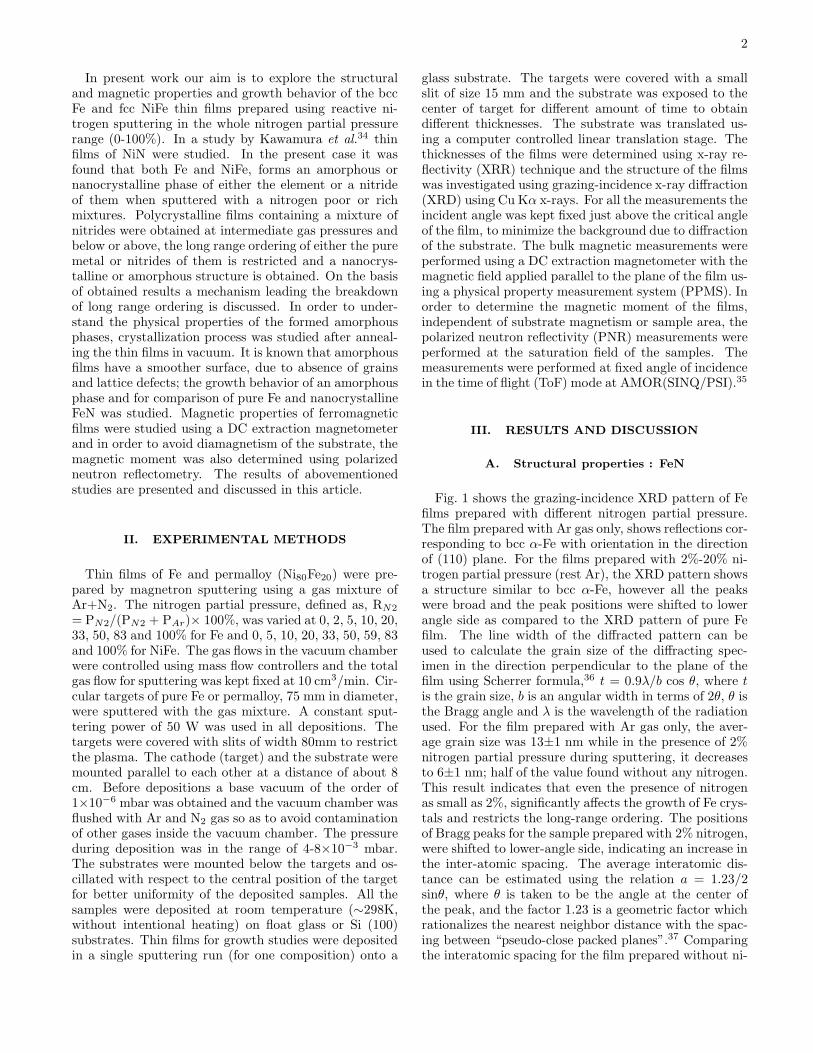
C. Crystallization behavior of amorphous films
From the observed XRD results it is evident that whennitrogen partial pressure during sputtering is 5 and 10%,an amorphous phase of FeN was formed while at 33%and above 50%, amorphous NiFeN phase was formed. Itwould be interesting to study the crystallization behaviorof these amorphous phases in order to understand theirproperties. Two sets of samples were chosen for crys-tallization studies (i) Fe-rich, FeN samples prepared atRN2 = 2, 5, 10 and 20% and (ii) N-rich, NiFeN sampleprepared at RN2 = 83%. These films were annealed in avacuum furnace isochronally for 1 hour at each tempera-ture. In order to avoid the fluctuations in temperature allthe four FeN films were annealed simultaneously in thevacuum furnace. Fig. 4(a-d) shows the grazing incidenceXRD pattern of FeN annealed films. It is interesting toobserve that the films prepared with 2 and 5% nitrogenpartial pressure were highly unstable, and even at 150◦C, Bragg peaks corresponding to α′′-FeN appear in theXRD pattern. The film prepared with RN2 = 10%, wasfound to be more stable and it remained amorphous up toan annealing temperature of 200 ◦C. On further anneal-ing at 300 ◦C the amorphous hump splits into three sharppeaks corresponding to ǫ-Fe2N1−z phase and at 400 ◦C,new peaks corresponding to α′′-Fe16N2 phase were ob-served. For the film prepared with RN2 = 20%, the XRDpattern reveals a composite structure consisting of amor-phous bcc-Fe and ǫ-Fe2N1−z phase in the as-depositedstate and after annealing at 150 ◦C, the structure crys-
5
20 30 40 50 60 70 80 90 100
150 oC
RN2
=2%
Inte
nsity
(ar
b. u
nits
)
2 (degree)
as-depo. (a)
'' FeN
Fe
20 30 40 50 60 70 80 90 100
Inte
nsi
ty (
arb
. u
nits
)
2 (degree)
" FeN
150 oC
RN2
=5%
as-depo.
Fe
(b)
20 30 40 50 60 70 80 90
2 (degree)
Inte
nsity
(arb
. uni
ts)
400 oC
300 oC
200 oC
(c)
RN2
=10%
as-depo.
150 oC
-FeFe
2N
1-z''-Fe
16N
2
20 30 40 50 60 70 80 90
300 oC
150 oC
(d)
RN2
=20%
In
tens
ity (
arb.
uni
ts)
2 (degree)
as-depo.
FeN
FIG. 5: Grazing incidence x-ray diffraction pattern of FeN film prepared with 2% (a), 5% (b), 10% (c) and 20% (d), in theas-deposited state and after vacuum annealing at various temperatures. The films were annealed isochronally for 1 hour.
tallizes into ǫ-Fe2N1−z phase. Observed crystallizationbehavior of amorphous phase shows that the amorphousphase shows a better stability for the film prepared withRN2 = 10%, and the films prepared either with higher orlower nitrogen are formed in a highly metastable state.Fig. 6 shows grazing incidence XRD pattern of the NiFeNfilm prepared at RN2 = 83%, after annealing at differenttemperatures. As can be seen from the figure, up to anannealing temperature of 250 ◦C, no significant changesin the XRD pattern were observed. While after annealingat 350 ◦C, several peaks were observed. The most intensepeaks corresponds to (FeNi)3N and γ′-FeNi3N phases.Smaller peaks at 53.6, 58.2 and 77.8◦ could not be iden-tified. After further annealing at 500 ◦C, no nitride phasewas observed, indicating out diffusion of nitrogen.
The observed crystallization behavior of both amor-phous FeN and NiFeN phases is different as compared toiron based binary or multi-component alloys. In conven-tional metal-metal amorphous alloys, generally crystal-lization occurs in 2 steps, in the first step a nanocrys-talline microstructure co-exists with parent amorphousphase whereas in the second step an intermetallic com-pound along with nanocrystalline phase precipitates out.The nominal reaction for such crystallization process
had been given as: amorphous → α+amorphous → α+β; where α is the primary phase that precipitates outfrom the amorphous matrix and β is an intermetalliccompound.38,39 In the present case, however, crystalliza-tion takes place in a single step and annealing at temper-atures above crystallization temperatures essentially re-sults in nitrogen out diffusion. The amorphous structureremained amorphous up to certain annealing tempera-ture and thereafter mixed nitride phase were observed.On further annealing due to nitrogen out diffusion puremetallic or nitrogen poor phases are obtained.
D. Surface properties and growth behavior of FeN
films
The thickness of FeN and NiFeN thin films depositedfor RN2 = 0-100%, were determined using x-ray re-flectivity technique. Since both FeN and NiFeN thinfilms were deposited in a similar manner, detailed sur-face and growth behavior of FeN thin films was inves-tigated. Fig. 7 shows x-ray reflectivity pattern of FeNthin films prepared at different nitrogen partial pressures.The x-ray reflectivity pattern was fitted using a computer

6
30 40 50 60 70 80 90 100
500 oC
300 oC
200 oC
2 (degree)
Inte
nsity
(arb
. uni
ts)
as-depo.
' FeNi3N
(FeNi)3N +
FeNi3
FIG. 6: Grazing incidence x-ray diffraction pattern of NiFeNthin film prepared with 83% nitrogen partial pressure afterannealing at different temperatures.
0.05 0.10 0.15 0.2010-6
10-4
10-2
1
102
104
106
108
measured fitted
83 %
50 %
20 %
2 %
X-ra
y re
flect
ivity
qz(Å-1)
0 %
10 %
FIG. 7: X-ray reflectivity pattern of FeN thin films preparedwith different nitrogen partial pressure.
program40 based on Parratt’s formalism.41 Oscillationsdue to total thickness of the films can be clearly seenin the reflectivity pattern. The thickness of the filmsobtained after fitting the pattern and was found in therange of 90-100 nm. The fitted parameters are given intable I. A detailed fitting of the pattern revealed that a
TABLE I: Fitted x-ray reflectivity parameters for FeN thinfilms prepared at different nitrogen partial pressures.
RN2 film film sub
thickness roughness roughness(%) nm(±0.2) nm(±0.1) nm(±0.2)0 103.5 3.3 0.62 105.4 2.0 0.610 101.6 0.4 0.620 98.3 1.0 0.650 93.5 1.0 0.683 113.5 0.8 0.6
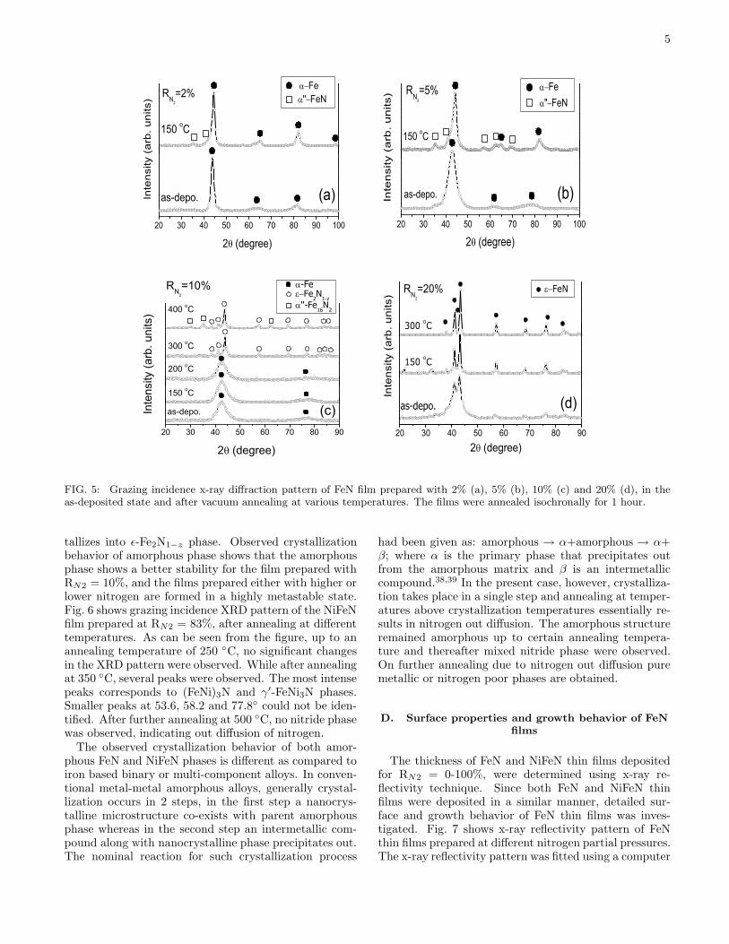
thin layer with density about 50% of the bulk of the lay-ers is formed on the surface. Such a layer may be formeddue to “oxidation” of the surface when exposed to atmo-sphere. The thickness of this layer was typically 2-3 nm.It is interesting to see that the roughness of the film pre-pared with Ar gas only, was 3.3 nm, which decreases to 2nm at RN2 = 2%, and was only 0.4 nm for RN2 = 10%.At RN2 = 20 and 50% the roughness again increases to1 nm and at 83% again it decreases slightly. While look-ing at microstructure of the deposited film obtained fromXRD measurements, there is a clear indication that anamorphous phase is formed at lower and higher nitrogenpartial pressures. A decrease in the roughness of filmis not unexpected since amorphous structure is free ofgrains and lattice defects, which may result in formationof a smoother surface or interface. With the observeddecrease in the roughness of the film for amorphous sam-ples, it would be interesting to study the growth behaviorof these films. For this purpose a series of FeN thin filmswere deposited at RN2 = 0, 10 and 83%. In order tominimize the parameters influencing the growth of a thinfilm, all the film with one composition were prepared in asingle sputtering run. For this purpose, the area of sput-tering target was masked with a small slit of size 15 mmand all the films were prepared on a glass substrate byexposing the substrate for different times to the plasmaat different positions on the substrate to obtain differentthicknesses.
All the films were prepared in the thickness range of 10-150 nm. X-ray reflectivity measurements on all the filmswere performed in specular and off-specular mode. Theoff-set in off-specular measurements was taken at the on-set of specular reflection peak in the rocking scan. Thisoffset was 0.05◦. The off-specular data was subtractedfrom the specular data to obtain the “true-specular”data. Fig. 8(a-c) shows the XRR patterns of abovemen-tioned thin films. The patterns were fitted using a pro-cedure as describe earlier. It was observed that for pureiron film, the surface roughness increases monotonicallywith an increase in the thickness while for the amorphousFeN film the roughness of the film increases at a very slowrate. For the case when FeN forms a nanocrystalline ni-tride at RN2 = 83%, the surface roughness again showan increase with the thickness. Previous studies have
7
0.1 0.210-5
10-1
103
107
1011
measured fitted
Fe, 0 % N2
18 min
qz(Å-1
)
X-ra
y re
flect
ivity
1 min
3 min
5 min6min
9 min
12 min
15 min
(a)0.08 0.16 0.24
10-5
10-1
103
107
1011
qz(Å-1
)
measured fitted
FeN, 10 % N2
X-ra
y re
flect
ivity
1 min3 min
5 min
6min
9 min
12 min
15 min
(b)
0.1 0.2 0.310-6
10-2
102
106
1010
1014
qz(Å-1
)
measured fitted
FeN, 83 % N2
X-ra
y re
flect
ivity
2min
4min
7min
10min
14min
19min
25min
30min
(c)
10 1000.2
0.4
0.6
0.8
1 FeN (10%), =0.14 Fe, =0.34 FeN (80%), =0.39
Rou
ghne
ss (n
m)
Thickness (nm)
(d)
FIG. 8: X-ray reflectivity pattern of pure Fe film (a), FeN film with 10% N (b) and FeN film with 83% nitrogen partial pressure(c). The evolution of film roughness with film thickness (d).

8
shown that the rms roughness (σ) exhibits a power-lawbehavior,20,42 as a function of the film thickness, givenas: σ ∼ tβ , accordingly, a double logarithmic plot ofthe rms roughness of the films versus the film thicknessshould yield a linear relation. Fig. 8(d) shows a plotrms roughness versus film thickness for the abovemen-tioned samples and a straight line fit to the data yieldsthe roughness growth exponent,β. For pure Fe film β =0.35, for amorphous FeN film prepared at RN2 = 10%,β = 0.14, and for nanocrystalline FeN film prepared atRN2 = 83%, β = 0.39. The value of β for amorphous FeNis very close to that obtained for amorphous SiO2
43 andnitrogen rich amorphous FeN prepared using ion-beamsputtering.20 Under the various growth models describedin literature, it may be observed that for the values of theroughness growth exponent lying in the range of 0.1-0.25,the growth can be well described by the KPZ model, firstintroduced by Kardar, Parisi, and Zhang.44 This type ofthe growth processes takes into account a random de-position and a limited relaxation of the particles at thesurface. For the present case the value of for amorphoussample lies well in this range, while for both pure Feand nanocrystalline FeN, the value of β is higher. Ahigher value of β indicates non KPZ type growth whichis often observed for polycrystalline elements. The ob-tained results clearly show a different growth mechanismfor amorphous film and support the argument that amor-phous films yield smoother surfaces. It may be notedthat the absolute roughnesses of the films prepared withsmaller slits (15 mm) in front of the targets were smalleras compared with the larger slits (80 mm).
E. Bulk magnetization measurements of FeN and
NiFeN films
Fig. 9 shows MH curve of the FeN samples prepared atdifferent nitrogen partial pressure. For the film preparedwith Ar gas only, the behavior is as-expected for iron,and the value of saturation magnetization (Ms) was al-most equal to reported values for bulk Fe. For the sampleprepared at RN2 = 2%, the MH loop shape changes to atypical soft-magnetic. While the value of saturation mag-netization is almost equal to pure Fe, the MH curve showsa significant decrease in the value of coercivity (Hc). Itmay be noted that the average grain size (D) for pureFe is about 13 nm, while for the sample prepared with2% nitrogen partial pressure, the grain size reduce to 6nm. A decrease in Hc in nanocrystalline ferromagnets isexpected as envisaged in the random-anisotropy model(RAM).45,46,47 It may be noted that the ferromagneticexchange length (Lex) for α-Fe is 15-23 nm.48,49For grainsizes D < Lex, Hc decreases with a decrease in grainsize by D6. A reduction in grain size below ferromag-netic exchange length allows exchange coupling betweenthe neighboring grains and results in a reduced effectiveanisotropy 〈K〉. In the present case, however, the de-crease in Hc was not found to vary with D6, rather it fol-
-75 -50 -25 0 25 50 75
-1500
-750
0
750
1500
M (e
mu/
cc)
H (Oe)
0 % 2 % 10 % 20 % 33%
0 10 200
20
40
60
Hc
(Oe)
N2 (%)
FIG. 9: Magnetization measurements of FeN thin films pre-pared at different nitrogen partial pressures. The inset showsa variation in coercivity as a function of nitrogen partial pres-sure during sputtering.
lows D2−3 type behavior. Since in the present case thick-ness of the films is small, it is likely that effective averag-ing would be only in the plane (area) of the film. In thissituation the ferromagnetic correlation volume would beproportional to Lex
2 only, in contrast to Lex3, in case of
bulk materials. This would reduce the number of grainsover which the averaging is done, and therefore a reduc-tion in the magnetic anisotropy and Hc is not expectedto vary as D6 as observed in nanocrystalline ribbons orpowders. Assuming averaging over N=(Lex/D)2 numberof grains, the effective anisotropy would be:
〈K〉 =K2
1D2
A, (1)
where K1 is magneto-crystalline anisotropy of the grainsand A is the exchange stiffness. This would mean thatin case of a thin film, Hc would follow D2 type behaviorrather than D6, as pointed out by Hoffmann et al.
50 Theobserved decrease in Hc, for the sample prepared in pres-ence of 2% nitrogen partial pressure can be understoodaccordingly.
On the other hand when nitrogen partial pressure wasincreased to 10%, the alloy forms an amorphous structureand the magnetic measurements show a decrease in Ms aswell as Hc. A decrease in Hc can be understood withinRAM, when averaging is done on very fine grains andmagnetization follow the easy direction of each individualgrain. The decrease in the value of Ms can be understooddue to weakening of the exchange coupling between thegrains. Further, at RN2 = 20%, the Hc increase abruptlywhile Ms continues to decrease.
It may be noted that at this nitrogen partial pressureamorphous phase co-exists with hcp-ǫ-Fe3N phase. Incase ǫ-Fe3N phase is nonmagnetic (as found at higherRN2), presence of a nonmagnetic phase among the fer-romagnetic fine grains would result in a decrease in

9
exchange length, which in accordance with the RAM,causes anisotropy and coercivity to increase because of in-complete averaging-out of random anisotropies of grainswithin the exchange volume. The observed increase inthe Hc and decrease in Ms can be understood with thisargument. At further higher nitrogen partial pressurewhere ǫ-Fe3N phase along with ζ-Fe2N phases were ob-tained, the magnetization was almost zero, indicatingnonmagnetic nature of the film at this nitrogen pressure.The films deposited at even higher RN2 were also non-magnetic.
Crystallization behavior of the amorphous film de-posited at RN2 = 10%, was also studied with magne-tization measurements of the samples annealed at differ-ent temperatures. Fig. 10 shows magnetization measure-
-300 -200 -100 0 100 200 300
-1000
-500
0
500
1000
M(e
mu/
cc)
H(Oe)
as-depo. 150 oC 300 oC 400 oC
FIG. 10: Magnetization measurements of FeN thin film pre-pared at 10% nitrogen partial pressure as function of anneal-ing temperature.
ments after annealing at different temperatures as dis-cussed in the previous section. The M-H loop shape up,before crystallization temperature was similar to that inthe as-deposited state. The only appreciable change wasthe shape of the M-H loop, which became more square af-ter annealing. Such a change in the M-H loop shape is di-rectly related to removal of strains which might have de-veloped during the deposition. At higher annealing tem-perature where crystallization of amorphous phase takesplace, the loop shape was completely different. Therewas a sharp increase in the value of coercivity and theaverage value of Ms decreased. At further higher tem-perature, the value of Ms further decreased and the loopshape looks broader. From the XRD measurements it isevident that upon crystallization ǫ-Fe3N phase precipi-tates out and an increase in the Hc and decrease in Msis similar as observed for the sample prepared at RN2 =20%, where ǫ-Fe3N phase existed. The observed magne-tization behavior can be understood accordingly.
The magnetization measurements were also carried out
-300 -200 -100 0 100 200 300-600
-300
0
300
600
M (e
mu/
cc)
H (Oe)
0 % 5 % 10 %
-10 0 10
-400
0
400
FIG. 11: Magnetization measurements of NiFeN thin filmsprepared at different nitrogen partial pressures.
in NiFeN films as a function nitrogen partial pressure dur-ing sputtering. The M-H loop for the sample preparedwith Ar gas only is matching well with the values ob-tained for permalloy.51 For the samples prepared withincreased RN2, the magnetization decreases rapidly andthe values of coercivity increased (see Fig. 11). As willbe discussed later, the start structure with NiFe is fcc,and the volume of interstitial is much larger in case offcc as compared with a bcc Fe. This allows more nitro-gen atoms to be incorporated within the unit cell of fccNiFe, which eventually results in decrease in magnetiza-tion more rapidly as compared with bcc Fe. The observedmagnetization behavior may be understood with this ar-gument.
F. Polarized neutron reflectivity measurements
In the present case since the samples were depositedeither on glass or Si substrate and the thickness of thedeposited films was in the range of 100 nm, the diamag-netism of the substrates might results in erroneous val-ues of absolute saturation magnetization when measuredwith DC extraction magnetometer. Also the errors indetermining the size of the measured samples may leadto further errors in the values of absolute magnetization.With these two parameters in mind, the magnetizationof the FeN samples was also determined using Polarizedneutron reflectivity (PNR). PNR is a technique which isable to yield the absolute value of magnetic moment peratom in a magnetic thin film with high accuracy.52 Incontrast to bulk magnetization magnetometer technique(e.g. DC extraction, VSM or SQUID), no correction dueto magnetic signal from the substrate has to be appliedin PNR. Further, the samples dimensions and mass doesnot play a crucial role in determination of magnetic mo-
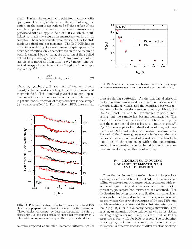
10
ment. During the experiment, polarized neutrons withspin parallel or antiparallel to the direction of magneti-zation on the sample are reflected-off the surface of thesample at grazing incidence. The measurements wereperformed with an applied field of 400 Oe, which is suf-ficient to reach the saturation magnetization in all thesamples. The measurements were carried out in the ToFmode at a fixed angle of incidence. The ToF-PNR has anadvantage as during the measurement of spin up and spindown reflectivities, only the polarization of the incomingbeam is changed by switching the direction of the appliedfield at the polarizing supermirror.35 No movement of thesample is required as often done in θ-2θ mode. The po-tential energy of a neutron in the ith region of the sampleis given by:52,53
Vi =2πh2
mn
ρibi + µn • Bi, (2)
where mn, ρi, bi, µn, Bi are mass of neutron, atomicdensity, coherent scattering length, neutron moment andmagnetic field. This potential gives rise to spin depen-dent reflectivity for the cases when incident polarizationis parallel to the direction of magnetization in the sample(+) or antiparallel (-). Fig. 12 shows PNR data on the
0.01
1
0.01 0.02 0.03 0.04
0.01
1
Pol
ariz
ed N
eutro
n R
efle
ctiv
ity
qz(Å-1)
0.01
1
0.01
1
0.01
1
0.01
1
0.01
1
50%
33%
20%
10%
5%
2%
0%
FeN
FIG. 12: Polarized neutron reflectivity measurements of FeNthin films prepared at different nitrogen partial pressures.Closed circles represents the data corresponding to spin upreflectivity R+ and open circles to spin down reflectivity R−.The solid line represents fitting to the experimental data.
samples prepared as function increased nitrogen partial
0 20 40 60 80 100
0.0
0.5
1.0
1.5
2.0
2.5
M (
B)
RN2
(%)
DC extraction PNR
bulk Fe
FIG. 13: Magnetic moment as obtained with the bulk mag-netization measurements and polarized neutron reflectivity.
pressure during sputtering. As the amount of nitrogenpartial pressure is increased, the edge in R− shows a shifttowards higher qz values, and the separation between R+and R− reflectivities decreases continuously. Finally forRN2>20, both R+ and R− are merged together, indi-cating that the sample has became nonmagnetic. Themagnetic moment in each case was determined by fit-ting the experimental data using a computer program.54
Fig. 13 shows a plot of obtained values of magnetic mo-ment with PNR and bulk magnetization measurements.Perusal of the figures gives a clear indication that thevalues of magnetic moment obtained with the two tech-niques lies in the same range within the experimentalerrors. It is interesting to note that at no point the mag-netic moment is higher than that of pure.
IV. MECHANISM INDUCING
NANOCRYSTALLIZATION OR
AMORPHIZATION
From the results and discussion given in the previoussection, it is clear that both Fe and NiFe form a nanocrys-talline or amorphous structures when sputtered with re-active nitrogen. Only at some specific nitrogen partialpressures, polycrystalline structures are obtained. Themechanism inducing nanocrystallization or amorphiza-tion can be understood in terms of incorporation of ni-trogen within the crystal structures of Fe and NiFe andrapid quenching of adatoms at the substrate. Atoms withlow Z e.g. B, C or N can easily occupy interstitial sitescausing an expansion of the unit cell as well as restrictingthe long range ordering. It may be noted that for Fe thestructure is bcc, while for NiFe, it is fcc. The probabilityof occupying the interstitial sites in the bcc and fcc crys-tal system is different because of different close packing.

11
In bcc-Fe the atoms may occupy the tetrahedral inter-
fcc
a0
(½,0
,0)
Rr
a0
r
½a0
¼a0
(¼,½,0)
R
bcc
FIG. 14: Distribution of interstitial site in bcc and fcc struc-tures.
stitial sites (see Fig. 14), such as (14, 12,0), while in a fcc
structure, nitrogen atom may be located either at theoctahedral sites at the edge center of unit cell (1
2, 0, 0)
and/or at the center of the unit cell (12, 12,12). The prob-
ability of occupation of nitrogen atoms at the interstitialsites in the two structures can be obtained by calculatingthe size of the interstitials for the two cases:
The radius of tetrahedral interstitial site at (14, 12,0) lo-
cation in bcc-Fe can be written as:
rint = [(1
2a0)
2 + (1
4a0)
2]1
2 − Rbcc, (3)
where Rbcc is the radius of bcc Fe and a0 (=0.2866 nm)is the lattice constant of the bcc Fe atom and Rbcc =√
3a0/4 = 0.1241 nm. From equation (3) the radius of(14, 12, 0) location of interstitial site rint for bcc Fe is 0.0361
nm. Similarly we can calculate the radius of interstitialsite for fcc NiFe at the octahedral sites (1
2, 0, 0) using
the expression:
2rint = a0 − 2Rfcc, (4)
Where a0 = 0.3545nm for NiFe and Rfcc is the radius of
fcc NiFe and Rfcc =√
2a0/4 = 0.1253 nm. From equation(4) the radius of (1
2, 0, 0) location of interstitial site rint
for fcc is 0.0523 nm.
The intestinal site in the bcc Fe is smaller than that infcc NiFe alloy. Whereas both are smaller than atomic ra-dius of nitrogen atom (0.075 nm). Therefore for both Feand NiFe, nitrogen occupying the interstitial sites wouldcause a distortion to the unit cell and it is expected thatthis distortion should be more effective for bcc Fe as com-pared with fcc NiFe while depositing at a given nitrogenpartial pressure. As a matter fact it is clear from ourXRD results that almost complete amorphization of Fewas observed at RN2 = 10%, while incase of NiFe, fullyamorphous state was obtained at RN2 = 33%. This resultclearly indicated that nitrogen atoms gradually occupythe interstitial space within bcc or fcc structure and sinceavailable space in a fcc structure is larger, fcc structure al-lowed more nitrogen atoms to be incorporated. Further,when nitrogen partial pressure was increased beyond theone at which final amorphous structure was obtained, thestructure of both Fe and NiFe was changed basically toA3N (A = Fe or NiFe).
From the energetics of binary iron nitrides55 (at roomtemperature), it may be noted that the heat of formationfor ǫ-Fe3Nx is lower (-40 to -45 kJ mol−1) as comparedwith neighboring e.g. Fe4N (-12 kJ mol−1) or Fe2N (-34kJ mol−1) phases. On the other hand nitrogen richestphase γ′′′-FeN0.91 has the lowest enthalpy of formation(-47 kJ mol−1). It is expected that at intermediate nitro-gen pressures when no more interstitial nitrogen can beincorporated within the unit cell, Fe3N or Fe2N phaseswould be readily formed. In fact when sputtered withRN2 = 33%, iron nitride structure is a mixture of Fe3Nand Fe2N phases. Further increase in nitrogen partialpressure at 50%, resulted in formation of nitrogen richγ′′′-type FeN. Still since the peaks were broadened, com-pletely crystalline structure was not formed. At RN2 =83%, sharp reflections corresponding to γ′′′-FeN were ob-served. A further increase in the nitrogen partial pressureresulted in broadening of the XRD peaks. This meansthat well-defined polycrystalline structure of FeN com-pounds are only obtained at some specific nitrogen par-tial pressures and below and above these specific partialpressures the long range ordering is restricted due to in-complete Fe-N bonds or partial breaking of Fe-N bondsdue to excessive nitrogen. Similar behavior was also ob-served for NiFe, however amount of incorporation of ni-trogen atoms in the two cases is different.
The energy of the adatoms with parameters used dur-ing sputtering for Fe or NiFe would be around 10 eV,56
which corresponds to roughly 105 K. During condensa-tion onto the substrate which tales place within ∼msec,the adatoms are rapidly quenched, the mobility of theatoms is restricted; it is expected that either the occu-pancy of reactive nitrogen at interstitial sites or a chem-ical reaction between sputtered atom and nitrogen takesplace in the plasma. Since the substrate were not heatedintentionally, it is very unlikely that any rearrangementprocess would take place onto the substrate after conden-sation. This argument supports that microstructure ofthe deposited film would strongly depend on the plasma
12
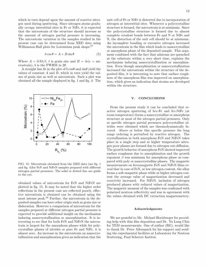
which in turn depend upon the amount of reactive nitro-gen used during sputtering. Since nitrogen atoms gradu-ally occupy interstitial sites in Fe or NiFe, it is expectedthat the microstrain of the structure should increase asthe amount of nitrogen partial pressure is increasing.The microstrain variation in the samples studied in thepresent case can be determined from XRD data usingWilliamson-Hall plots for Lorentzian peak shape:57
b cos θ = A + B sin θ (5)
Where A = 0.9λ/t, t is grain size and B = 4ǫ(ǫ = mi-crostrain), b is the FWHM in 2θ.
A straight line fit in the plot of b cosθ and sinθ yield thevalues of constant A and B, which in turn yield the val-ues of grain size as well as microstrain. Such a plot wasobtained all the sample displayed in fig. 1 and fig. 4. The
0 20 40 60 80 100
0
2
4
6
8
10 Ni80Fe20 Fe
Mic
rost
rain
(%)
RN2
(%)
FIG. 15: Microstrain obtained from the XRD data (see fig. 1and fig. 4)for FeN and NiFeN samples prepared with differentnitrogen partial pressures. The solid or dotted line are guideto the eye.
obtained values of microstrain for FeN and NiFeN areplotted in fig. 15. It may be noted that the higher orderreflections in the present case are reflected poorly, effec-tive microstrain is obtained can be obtained using themost intense peak.58 Further, the microstrain in the de-posited samples can have other origin such as grain size ordislocation. However a comparison of microstrain for thesamples prepared at different nitrogen partial pressure isexpected to provide additional insight on the mechanisminducing nanocrystallization or amorphization. It is in-teresting to see that for both FeN and NiFeN the micros-train is largest for the amorphous phases while for poly-crystalline phases of nitrides or pure Fe and NiFe, it isalmost zero. An increase in the microstrain on nanocrys-tallization and amorphization gives an indication that the
unit cell of Fe or NiFe is distorted due to incorporation ofnitrogen at interstitial sites. Whenever a polycrystallinestructure is formed, the microstrain is at minimum. Sincethe polycrystalline structure is formed due to almostcomplete covalent bonds between Fe and N or NiFe andN, the distortion of the unit cell should be at minimum.An incomplete bonding or excessive nitrogen increasedthe microstrain in the film which leads to nanocrystallineor amorphous phase of the deposited sample. This argu-ment combined with the fact that adatoms are quenchedat the substrate within a very short time, explains themechanism inducing nanocrystallization or amorphiza-tion. Even though amorphization or nanocrystallizationincreased the microstrain within the structure of the de-posited film, it is interesting to note that surface rough-ness of the amorphous film was improved on amorphiza-tion, which gives an indication that strains are developedwithin the structure.
V. CONCLUSIONS
From the present study it can be concluded that re-active nitrogen sputtering of bcc-Fe and fcc-NiFe (atroom temperature) forms a nanocrystalline or amorphousstructure at most of the nitrogen partial pressures. Onlyat specific nitrogen partial pressures polycrystalline ni-trides were obtained which are thermodynamically fa-vored. Above or below this specific pressure the longrange ordering is perturbed by reactive nitrogen. Thecrystallization in both amorphous FeN and NiFeN takesplace in a single step and at higher temperature nitro-gen poor phases are formed due to nitrogen out-diffusion.The growth behavior of amorphous FeN showed improvedsurface roughness due to amorphization and the growthexponent β was minimum for amorphous phase as com-pared with poly or nanocrystalline phases. The magneticmeasurements on ferromagnetic FeN and NiFeN films re-veal that in case of FeN, at low nitrogen content, the alloyforms a soft-magnetic phase while at higher nitrogen con-tent the average value of magnetization decreased andcoercivity increased. For NiFeN, inclusion of nitrogenproduced phases with reduced values of magnetization.The magnetic moment of the samples was confirmed withpolarized neutron reflectivity and was in agreement withthe values obtained with DC extraction magnetometery.
Acknowledgments
We are grateful to Mr. Michael Horisberger for provid-ing help with thin film deposition and Dr. Yu Lung Chiufor TEM measurements. One of author (RG), would liketo thank Dr. Peter Allenspach for his support and avail-ing the experimental facilities at Laboratory for NeutronScattering, Paul Scherrer Institut.

13
∗ Electronic address: [email protected] C. A. Angell, K. L. Ngai, G. B. McKenna, P. F. McMillan,
and S. W. Martin, J. Appl. Phys. 88, 3113 (2000).2 P. G. Debenedetti and F. H. Stillinger, Nature 410, 259
(2001).3 M. E. McHenry, M. A. Willard, and D. E. Laughlin, Prog.
Mat. Sci. 44, 291 (1999).4 A. Dunlop, G. Jaskierowicz, G. Rizza, and M. Kopcewicz,
Phys. Rev. Lett. 90, 015503 (2003).5 C. Line, D. Sun, S. L. Ming, E. Jiang, and Y. Liu, Thin
Solid film 279, 49 (1996).6 N. Sulitanu and F. Brinza, J. Opto Elec. Adv. Mat 5, 421
(2003).7 F. Faupel, W. Frank, M. P. Macht, H. Mehrer, K. Ratzke,
H. Schober, S. K. Sharma, and H. Teichler, Rev. Mod.Phys. 75, 237 (2003).
8 S. R. Elliott, Physics of Amophouse Materials (LongmanScientific and Tachnical, 1990), 2nd ed.
9 C. C. Koch, O. B. Cavin, C. G. McKamey, and J. O. Scar-brough, Appl. Phys. Lett. 43, 1017 (1983).
10 W. J. Meng, P. R. Okamoto, L. J. Thompson, B. J. Kestel,and L. E. Rehn, Appl. Phys. Lett. 53, 1820 (1988).
11 S. M. Sharma and A. K. Sikka, Prog. Mater. Sci. 40, 1(1996).
12 R. B. Schwarz and W. L. Johnson, Phys. Rev. Lett. 51,415 (1983).
13 W. L. Johnson, Prog. Mater. Sci. 28, 229 (1985).14 K. Samwer, Phys. Rep. 161, 1 (1988).15 M. Holz, P. Ziemann, and W. Buckel, Phys. Rev. Lett. 51,
1584 (1983).16 S. Takeda and J. Yamasaki, Phys. Rev. Lett. 83, 320
(1999).17 N. Hellgren, M. P. Johansson, E. Broitman, L. Hultman,
and J.-E. Sundgren, Phys. Rev. 59, 5162 (1999).18 D. Babonneau, M. Jaouen, M.-F. Denanot, P. Guerin, and
F. Petroff, App. Phys. Lett. 82, 30565 (2003).19 M. Gupta, A. Gupta, S. Rajagopalan, and A. K. Tyagi,
Phys. Rev. B 65, 214204 (2002).20 A. Gupta, M. Gupta, B. A. Dasannacharya, S. Kikuta,
Y. Yoda, and M. Seto, J. Jpn. Phys. Soc. 73, 423 (2004).21 L. Rissanen, M. Neubauer, K. P. Lieb, and P. Schaaf, J.
Alloys and Compds. 274, 74 (1998).22 M. A. Russak, C. V. Jahnes, E. Klokholm, J.-W. Lee, M. E.
Re, and B. C. Webb, J. Appl. Phys. 70, 6427 (1991).23 J.-F. Bobo, H. Chatbi, M. Vergnat, L. Hennet, O. Lenoble,
P. Bauer, and M. Piecuch, J. Appl. Phys. 77, 5309 (1995).24 H. B. Nie, S. X. Xu, C. K. Ong, Q. Zhan, D. X. Li, and
J. P. Wang, Thin Solid Films 440, 35 (2003).25 T. Yoshitake and M. Ohkoshi, I.E.E.E. Trans. Magn 31,
3850 (1995).26 M. Gupta, A. Gupta, P. Bhattacharya, P. Misra, and L. M.
Kukreja, J. Alloys and Compds. 326, 265 (2001).27 N. Wang, K. M. Ulmer, P. A. Constant, J. W. Anderegg,
and J. E. Snyder, J. Vac. Sci. Technol. A 21, 1734 (2003).28 L. Guibin, L. Guoqing, L. Minaki, and L. Bangzhi, Sur.
Coat. Technol. 96, 34 (1997).29 T. Kim and M. Takahashi, Appl. Phys. Lett. 20, 492
(1972).30 Y. D. Zhang, J. I. Budnick, W. A. Hines, M. Q. Huang,
and W. E. Wallace, Phys. Rev. B 54, 51 (1996).
31 C. Chang, J. M. Sivertsen, and J. H. Judy, I.E.E.E. Trans.Mag. MAG 23, 3636 (1987).
32 X. Wang, W. T. Zheng, H. Tian, S. S. Yu, and L. L. Wang,J. Magn. Magn. Mat. 283, 282 (2004).
33 M. Chiba, K. Morio, and Y. Koizumi, J. Magn. Magn.Mat. 242, 949 (2002).
34 M. Kawamura, Y. Abe, and K. Sasaki, Vacuum 59, 721(2000).
35 M. Gupta, T. Gutberlet, J. Stahn, P. Keller, andD. Clemens, Pramana J. Phys 63, 57 (2004).
36 B. D. Cullity, Elements of X-ray Diffraction (Addison-Wesley,MA, 1978).
37 A. Guinier, X-Ray Diffraction : In Crystals, Imperfect
Crystals and Amorphous Bodies (Dover, New York, 1994).38 K. Hono and D. H. Ping, Materials Characterization 44,
203 (2000).39 D. M. Zhu, K. Raviprasad, K. Suzuki, and S. P. Ringer, J.
Phys. D:Appl. Phys. 37, 645 (2004).40 C. Braun, Parratt32- The Reflectivity Tool (HMI Berlin,
1997-99).41 L. G. Parratt, Phys. Rev. 95, 359 (1954).42 A. L. Barabasi and H. E. Stanley, Fractal Concepts in Sur-
face Growth (Cambridge University Press, 1995).43 M. Lutt, J. P. Schlomka, M. Tolan, J. Stettner, O. H.
Seeck, and W. Press, Phys. Rev. B 56, 4085 (1997).44 M. Kardar, G. Parisi, and Y.-C. Zhang, Phys. Rev. Lett.
56, 889 (1986).45 G. Herzer, I.E.E.E. Trans. Mag. 25, 3327 (1989).46 G. Herzer, I.E.E.E. Trans. Mag. 26, 1397 (1990).47 J. F. Loffler, J. P. Meier, B. Doudin, J.-P. Ansermet, and
W. Wagner, Phys. Rev. B 57, 2915 (1998).48 R. W. Gao, W. C. Feng, H. Q. Liu, B. Wang, W. Chen,
G. B. Han, P. Zhang, H. Li, W. Li, Y. Q. Guo, et al., J.Appl. Phys. 94, 664 (2003).
49 J. F. Loffler, H.-B. Braun, and W. Wagner, Phys. Rev.Lett. 85, 1990 (2000).
50 H. Hoffmann and T. Fujii, J. Magn. Magn. Mat 128, 395(1993).
51 B. D. Cullity, Introduction to Magnetic Materials
(Addison-Wesley,MA, 1972).52 S. J. Blundell and J. A. C. Bland, Phys. Rev. B 46, 3391
(1992).53 S. Hope, J. Lee, P. Rosenbusch, G. Lauhoff, J. A. C. Bland,
A. Ercole, D. Bucknall, J. Penfold, H. J. Lauter, V. Lauter,et al., Phys. Rev. B 55, 11422 (1997).
54 F. Ott, SIMULREFLEC,http://www-llb.cea.fr/prism/programs/simulreflec/simulreflec.html.
55 F. Tessier, A. Navrotsky, R. Niewa, A. Leineweber, H. Ja-cobs, S. Kikkawa, M. Takahashi, F. Kanamaru, and F. J.DiSalvo, Solid State Sciences 2 (2000).
56 G. M. Turner, I. S. Falconer, B. W. James, and D. R.McKenzie, J. Vac. Sci. Technol. A 10, 455 (1992).
57 Y. Rosenberg, V. S. Machavariani, A. Voronel, S. Garber,A. Rubshtein, A. I. Frenkel, and E. A. Stern, J. Phys.:Condens. Matter 12, 8081 (2000).
58 L. R. Shaginyan, M. Misina, J. Zemek, J. Musil, F. Regent,and V. F. Britun, Thin Solid Films 408, 136 (2002).
Copyright © 2022 FDOKUMEN