MOPS/520 - Nooelec
88
MOPS/520 User’s Guide Document Revision 2.4
-
Upload
khangminh22 -
Category
Documents
-
view
8 -
download
0
Transcript of MOPS/520 - Nooelec

MOPS/520User’s Guide
Document Revision 2.4


Kontron
MOPS/520 User’s Guide Contentsi
CONTENTS
1. USER INFORMATION...............................................................................................11.1 About This Manual.......................................................................................11.2 Copyright Notice.........................................................................................11.3 Trademarks................................................................................................21.4 Standards..................................................................................................21.5 Warranty...................................................................................................21.6 Technical Support .......................................................................................3
2. INTRODUCTION .....................................................................................................42.1 MOPS/520 .................................................................................................42.2 The MOPS Family .........................................................................................52.3 PC/104 an Embedded PC Standard ..................................................................6
3. GETTING STARTED ..................................................................................................7
4. SPECIFICATIONS....................................................................................................84.1 Functional Specifications ..............................................................................84.2 Mechanical Specifications.............................................................................9
4.2.1. PC/104 Bus Connector (ISA part) ................................................................94.2.2. PC/104-Plus Bus Connector (optional PCI part) ..............................................94.2.3. PCB Dimensions.......................................................................................94.2.4. Height...................................................................................................94.2.5. Weight ..................................................................................................9
4.3 Electrical Specifications.............................................................................. 104.3.1. Supply Voltage ...................................................................................... 104.3.2. Supply Voltage Ripple ............................................................................. 104.3.3. Supply Current (Typical) .......................................................................... 104.3.4. Supply Current (Maximum) ...................................................................... 104.3.5. External RTC Battery............................................................................... 10
4.4 MTBF ...................................................................................................... 114.5 Environmental Specifications ...................................................................... 11
4.5.1. Temperature......................................................................................... 114.5.2. Humidity.............................................................................................. 11
5. CPU, CHIPSET, SUPER-I/O CONTROLLER ................................................................... 125.1 CPU and Chipset........................................................................................ 125.2 CPU and Chipset Configuration..................................................................... 135.3 Super I/O Controller .................................................................................. 135.4 Super I/O Controller Configuration ............................................................... 13
6. SYSTEM MEMORY .................................................................................................14
7. ISA AND PCI BUS EXPANSION .................................................................................15

Kontron
Contents ii MOPS/520 User’s Guide
7.1 PC/104 Bus (ISA part)................................................................................ 157.1.1. PC/104 Connectors ................................................................................ 157.1.2. PC/104 Configuration ............................................................................. 167.1.3. I/O Address Mapping Limitation................................................................ 167.1.4. Signal Limitations.................................................................................. 16
7.2 PC/104-Plus (optional PCI part) ................................................................... 167.2.1. PCI Connector (PC/104-Plus).................................................................... 167.2.2. PC/104-Plus Configuration ...................................................................... 17
7.3 PC/104 and PC/104-Plus Stack ..................................................................... 17
8. SERIAL-COMMUNICATION INTERFACE ......................................................................188.1 Connectors .............................................................................................. 188.2 Configuration........................................................................................... 198.3 Limitations.............................................................................................. 20
9. PARALLEL-COMMUNICATION INTERFACE ..................................................................219.1 Connector ............................................................................................... 219.2 Configuration........................................................................................... 229.3 Limitations.............................................................................................. 22
10. KEYBOARD AND FEATURE INTERFACE .......................................................................2310.1 Connector ............................................................................................... 2310.2 Configuration........................................................................................... 2510.3 Signal Descriptions.................................................................................... 25
10.3.1. Example Connection AT-keyboard and Other Functions................................... 26
11. PS/2 MOUSE INTERFACE........................................................................................2711.1 Connector ............................................................................................... 2711.2 Configuration........................................................................................... 27
12. USB INTERFACE................................................................................................... 2812.1 Connector ............................................................................................... 2812.2 Configuration........................................................................................... 2812.3 Limitations.............................................................................................. 28
13. FLOPPY-DRIVE INTERFACE .....................................................................................2913.1 Connector ............................................................................................... 29
13.1.1. Connector Diagram ................................................................................ 3013.2 Configuration........................................................................................... 30
14. IDE INTERFACE....................................................................................................3114.1 Connector ............................................................................................... 3114.2 Configuration........................................................................................... 32
15. ETHERNET INTERFACE ...........................................................................................3315.1 Connector ............................................................................................... 3315.2 Configuration........................................................................................... 3415.3 Ethernet Technical Support ......................................................................... 34

Kontron
MOPS/520 User’s Guide Contentsiii
16. POWER CONNECTION ............................................................................................ 3516.1 Connector ............................................................................................... 3516.2 Power Pins............................................................................................... 3616.3 External Battery........................................................................................ 37
17. CAN CONTROLLER INTERFACE (OPTIONAL)................................................................3817.1 Connector ............................................................................................... 3817.2 Configuration........................................................................................... 39
18. WATCHDOG TIMER ...............................................................................................4018.1 Configuration........................................................................................... 4018.2 Programming ........................................................................................... 40
18.2.1. Initialization ........................................................................................ 4018.2.2. Trigger ................................................................................................ 40
19. APPENDIX A: SYSTEM RESOURCE ALLOCATIONS..........................................................4119.1 Interrupt Request (IRQ) Lines...................................................................... 4119.2 Direct Memory Access (DMA) Channels ........................................................... 4219.3 Memory Map ............................................................................................ 43
19.3.1. Using Expanded Memory Managers ............................................................ 4419.4 I/O Address Map ....................................................................................... 4519.5 Peripheral Component Interconnect (PCI) Devices............................................ 46
20. APPENDIX B: BIOS OPERATION ...............................................................................4720.1 Determining the BIOS Version...................................................................... 4720.2 Setup Guide............................................................................................. 48
20.2.1. Start Phoenix BIOS Setup Utility ............................................................... 4820.2.2. General Information............................................................................... 48
20.3 Main Menu............................................................................................... 5020.3.1. Master or Slave Submenus ....................................................................... 5120.3.2. Memory Shadow Submenu ....................................................................... 51
20.4 Advanced Menu ........................................................................................ 5220.4.1. Advanced Chipset Control Submenu ........................................................... 5320.4.2. PCI Configuration Submenu ..................................................................... 5420.4.3. PCI Device, Slot #X Submenu .................................................................... 5520.4.4. PCI/PNP ISA UMB Region Exclusion Submenu............................................... 5520.4.5. PCI/PNP ISA IRQ Exclusion Submenu.......................................................... 5620.4.6. PCI/PNP ISA IRQ Exclusion Submenu.......................................................... 5620.4.7. Keyboard Features Submenu .................................................................... 5720.4.8. I/O Device Configuration Submenu ............................................................ 5720.4.9. Watchdog Settings Submenu.................................................................... 58
20.5 Security Menu .......................................................................................... 5920.6 Boot Menu............................................................................................... 60
20.6.1. Dark Boot............................................................................................. 6020.6.2. Boot Device Priority Submenu................................................................... 61
20.7 MultiBoot................................................................................................ 6220.7.1. Boot First Menu..................................................................................... 62
Kontron
Contents iv MOPS/520 User’s Guide
20.8 Exit Menu ................................................................................................ 6320.9 Kontron BIOS Extensions ............................................................................ 64
20.9.1. JIDA BIOS extension............................................................................... 6420.9.2. Remote Control Client Extension ............................................................... 6520.9.3. LAN RPL ROM ........................................................................................ 6520.9.4. DOT-Matrix LCD BIOS extension................................................................. 65
20.10 Updating or Restoring BIOS......................................................................... 6620.11 Preventing Problems When Updating or Restoring BIOS..................................... 67
21. APPENDIX C: BLOCK DIAGRAM ...............................................................................68
22. APPENDIX D: MECHANICAL DIMENSIONS..................................................................69
23. APPENDIX E: CONNECTOR LAYOUT ...........................................................................7123.1 Connector Locations .................................................................................. 7123.2 Connector Functions and Interface Cables ...................................................... 7223.3 Pinout Table............................................................................................. 73
24. APPENDIX F: LIMITATIONS AND HINTS.....................................................................7624.1 ISA Bus................................................................................................... 76
24.1.1. Available ISA Signals.............................................................................. 7624.1.2. I/O Address Mapping.............................................................................. 7624.1.3. ISA SCSI Support ................................................................................... 76
24.2 PCI Bus ................................................................................................... 7624.3 Serial Ports.............................................................................................. 7724.4 Parallel Port............................................................................................. 7724.5 USB Port ................................................................................................. 7724.6 System-Clock Deviation .............................................................................. 7724.7 Windows2000 Support ............................................................................. 7824.8 Watchdog Timer NMI Handling ..................................................................... 78
25. APPENDIX G: PC ARCHITECTURE INFORMATION..........................................................7925.1 Buses ..................................................................................................... 79
25.1.1. ISA, Standard PS/2 - Connectors ............................................................... 7925.1.2. PC/104, PCI - Information........................................................................ 79
25.2 General PC Architecture.............................................................................. 8025.3 Ports ...................................................................................................... 80
25.3.1. RS-232 Serial........................................................................................ 8025.3.2. ATA..................................................................................................... 8025.3.3. USB .................................................................................................... 81
25.4 Programming ........................................................................................... 81
26. APPENDIX H: DOCUMENT-REVISION HISTORY ............................................................ 82
This page left blank intentionally.

Kontron
MOPS/520 User’s Guide User Information1
1. USER INFORMATION
1.1 About This ManualThis document provides information about products from Kontron Embedded Modules AGand/or its subsidiaries. No warranty of suitability, purpose, or fitness is implied. While everyattempt has been made to ensure that the information in this document is accurate, theinformation contained within is supplied “as-is” and is subject to change without notice.
For the circuits, descriptions and tables indicated, Kontron assumes no responsibility as far aspatents or other rights of third parties are concerned.
1.2 Copyright NoticeCopyright © 2003 Kontron Embedded Modules AG.
All rights reserved. No part of this manual may be reproduced, transmitted, transcribed, stored ina retrieval system, or translated into any language or computer language, in any form or by anymeans (electronic, mechanical, photocopying, recording, or otherwise), without the expresswritten permission of Kontron.
JUMPtec Industrielle Computertechnik AG and Kontron Embedded Computers AG merged inJuly 2002. JUMPtec is now known as Kontron Embedded Modules GmbH. Products labeled andsold under the Kontron Embedded Modules name (formerly JUMPtec) are now consideredKontron products for all practical purposes, including warranty and support.
DIMM-PC®, PISA®, ETX Components SBC, JUMPtec®, and Kontron Embedded Modules areregistered trademarks of Kontron Embedded Modules GmbH©.

Kontron
User Information 2 MOPS/520 User’s Guide
1.3 TrademarksThe following lists the trademarks of components used in this board.
IBM, XT, AT, PS/2 and Personal System/2 are trademarks of International BusinessMachines Corp.
Microsoft is a registered trademark of Microsoft Corp.
Intel is a registered trademark of Intel Corp.
All other products and trademarks mentioned in this manual are trademarks of theirrespective owners.
1.4 StandardsKontron Embedded Modules is certified to ISO 9000 standards.
1.5 WarrantyThis Kontron Embedded Modules product is warranted against defects in material andworkmanship for the warranty period from the date of shipment. During the warranty period,Kontron Embedded Modules will at its discretion decide to repair or replace defective products.
Within the warranty period, the repair of products is free of charge as long as warranty conditionsare observed.
The warranty does not apply to defects resulting from improper or inadequate maintenance orhandling by the buyer, unauthorized modification or misuse, operation outside of the product’senvironmental specifications or improper installation or maintenance.
Kontron Embedded Modules will not be responsible for any defects or damages to other productsnot supplied by Kontron Embedded Modules that are caused by a faulty Kontron EmbeddedModules product.

Kontron
MOPS/520 User’s Guide User Information3
1.6 Technical SupportTechnicians and engineers from Kontron Embedded Modules and/or its subsidiaries and officialdistributors are available for technical support. We are committed to making our product easy touse and will help you use our products in your systems.
Before contacting Kontron Embedded Modules technical support, please contact your localrepresentative or consult our Web site for the latest product documentation, utilities, and drivers.If the information does not help to solve the problem, contact us by telephone.
Asia Europe North/South AmericaKontron Embedded
Technology (Asia Pacific)Kontron Embedded Modules GmbH Kontron America
Far East Science Park, 2ndFloor No. 2, Lane 50, NanKang Road Section 3, Nan
Kang District Taipei, Taiwan
Brunnwiesenstr. 1694469 Deggendorf – Germany
6260 Sequence DriveSan Diego, CA 92121-4371
Tel: +886-2-2782-0201 Tel: +49 (0) 991-37024-0 Tel: 888-294-4558
Fax: +886-2-2782-7486 Fax: +49 (0) 991-37024-104 Fax: (858) 677-0898

Kontron
Introduction 4 MOPS/520 User’s Guide
2. INTRODUCTION
2.1 MOPS/520The MOPS/520 is based on the ÉlanSC520 microcontroller (32-bit Am5x86® CPU). The systemruns at CPU clock speeds of 100MHz or 133MHz. The boards integrate the completefunctionality of a motherboard and include the following features:
CPU
System BIOS
Up to 64MB SDRAM
Keyboard controller
Real-time clock
Additional peripheral functions include:
COM1, COM2, COM3 and COM4
LPT1
Floppy interface
IDE-hard disk interface
Watchdog time (WDT)
Ethernet controller
CAN bus interface (optional)
The MOPS/520 is not equipped with a graphics controller and requires an external graphics-controller board on the PC/104 or PC/104+ bus to provide output to a CRT monitor.

Kontron
MOPS/520 User’s Guide Introduction5
2.2 The MOPS FamilyMOPS (Minimized Open PC System) PC/104 products represent the “Proven PC Platform forInstant Solutions." Each MOPS module is characterized by the same pinout for the keyboard,COM1 and COM2, 44-pin IDE, LPT, and 1st LAN. These homogeneous features facilitate easyupgrades within the Kontron Embedded Modules GmbH MOPS PC/104 product family.
Whenever a LCD panel is required, MOPS products with onboard graphics controllers serve asthe right choice. Display connections are simplified when using these units, which come with aJUMPtec Intelligent LVDS Interface (JILI) and a JUMPtec Intelligent Panel Adapter (JIPA)interface. The two interfaces can recognize which display is connected and then independently setall video parameters. These interfaces are not available on all MOPS products.
All MOPS-PC/104 are plug-and-work enabled to further reduce time-to-market.
As part of the standard features package, all MOPS PC/104 modules come with a JUMPtecIntelligent Device Architecture (JIDA) interface, which is integrated into the BIOS of the PC/104modules. This interface enables hardware independent access to the MOPS-PC/104 features thatcannot be accessed via standard APIs. Functions such as watchdog timer, brightness and contrastof LCD backlight and user bytes in the EEPROM can be configured with ease by takingadvantage of this standard MOPS PC/104 module feature.
All MOPS PC/104 products can be remote controlled by using JRC software feature. This allowsyou to change, update, and maintain the MOPS products from a host computer via a serialconnection.

Kontron
Introduction 6 MOPS/520 User’s Guide
2.3 PC/104 an Embedded PC StandardOver the past decade, PC architecture has become an accepted platform for far more than desktopapplications. Dedicated and embedded applications for PCs are beginning to appear everywhere.
By standardizing hardware and software around the broadly supported PC architecture, embeddedsystem designers can substantially reduce development costs, risks, and time-to-market.
For these reasons, companies that embed microcomputers as controllers within their productsseek ways to reap the benefits of using the PC architecture. However, the standard form factor ofa PC bus (12.4" x 4.8") and its associated card cages and backplanes are too bulky and expensivefor most embedded control applications.
The only practical way to embed the PC architecture in space-and power-sensitive applicationshas been to design a PC chip by chip directly into the product. But this runs counter to growingtrend away from "reinventing the wheel." Whenever possible, top management now encouragesoutsourcing of components and technologies to reduce development costs and accelerate productdesign cycles.
A need has arisen for a more compact implementation of the PC bus, satisfying the reduced spaceand power constraints of embedded control applications. PC/104 was developed in response tothis need. It offers full architecture, hardware and software compatibility with the PC bus but inultra-compact (3.6" x 3.8") stackable modules. PC/104 is ideally suited to the uniquerequirements of embedded control applications.
Although configuration and application possibilities with PC/104 modules are practicallylimitless, there are two ways to use them in embedded system designs:
Standalone module stacksPC/104 modules are self-stacking. The modules are used like ultra-compact bus boardsbut without a need for backplanes or card cages. Stacked modules are spaced 0.6inches apart. (The three-module stack measures 3.6 by 3.8 by 2 inches.) Companiesusing PC/104 module stacks within their products frequently create one or more oftheir own application-specific PC/104 modules.
Component-line applicationsIn this configuration, the modules function as highly integrated components, pluggedinto custom carrier boards that contain application-specific interfaces and logic. Themodules' self-stacking bus can be useful to install multiple modules in one location.This facilitates product upgrades or options and allows temporary addition of modulesduring system debug or test.

Kontron
MOPS/520 User’s Guide Getting Started7
3. GETTING STARTED
The easiest way to get the MOPS/520 board running is to use a starter kit from KontronEmbedded Modules GmbH. Take the following steps:
1. Turn off the power supply (part of the starter kit).
2. Connect the power supply to the starter kit baseboard (part of the starter kit).
3. Plug a graphics-controller board to the PC/104 bus, the ISA bus slots, the PC/104-Plus bus or the PCI bus slots on the starter kit. (There are starter kits available withand without PC/104 graphics boards included.)
4. Connect the CRT monitor to the graphics controller board.
5. Plug the MOPS/520 to the PC/104 bus stack on the starter kit baseboard.
6. Make all necessary connections from the MOPS/520 to the starter kit board.(Cables come with the starter kit). The starter kit board offers various interfaces onstandard connectors.
7. Plug a keyboard to the starter kit’s keyboard connector.
8. Connect the floppy drive (part of the starter kit) with the data cable (part of thestarter kit) to the MOPS/520 floppy interface.
9. Connect the power supply to the floppy’s power connector.
10. Plug a hard-drive data cable to the MOPS/520 hard-disk interface. Attach the harddisk to the connector at the opposite end of the cable.
11. If necessary, connect the power supply to the hard disk’s power connector.
12. Make sure all your connections have been done correctly.
13. Turn on the power.
14. Enter the BIOS by pressing the F2 key during bootup. Make all necessary changes inthe BIOS setup. See the BIOS chapter of this manual for details.
Kontron
Specifications 8 MOPS/520 User’s Guide
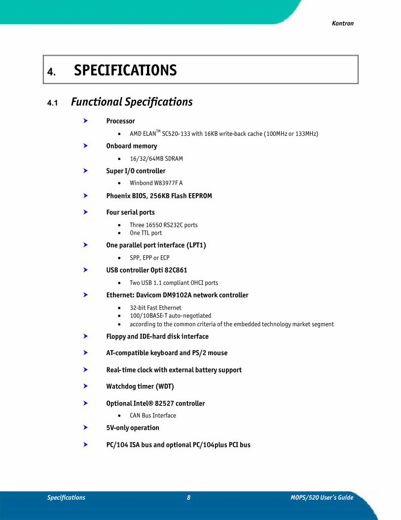
4. SPECIFICATIONS
4.1 Functional Specifications Processor
AMD ELANTM SC520-133 with 16KB write-back cache (100MHz or 133MHz)
Onboard memory
16/32/64MB SDRAM
Super I/O controller
Winbond W83977F A
Phoenix BIOS, 256KB Flash EEPROM
Four serial ports
Three 16550 RS232C ports One TTL port
One parallel port interface (LPT1)
SPP, EPP or ECP
USB controller Opti 82C861
Two USB 1.1 compliant OHCI ports
Ethernet: Davicom DM9102A network controller
32-bit Fast Ethernet 100/10BASE-T auto-negotiated according to the common criteria of the embedded technology market segment
Floppy and IDE-hard disk interface
AT-compatible keyboard and PS/2 mouse
Real-time clock with external battery support
Watchdog timer (WDT)
Optional Intel® 82527 controller
CAN Bus Interface
5V-only operation
PC/104 ISA bus and optional PC/104plus PCI bus

Kontron
MOPS/520 User’s Guide 9 Specifications
4.2 Mechanical Specifications
4.2.1. PC/104 Bus Connector (ISA part)
One 2 X 32 pin stackthrough and one 2 X 20 pin stackthrough connector
4.2.2. PC/104-Plus Bus Connector (optional PCI part)
PC/104plus: 4 x 30 pin 2mm connector
The PC/104plus connector does not have a connector shroud. You cannot use a PC/104plus boardwith a connector shroud on the top of a MOPS/520. This mechanical limitation does not reducethe functionality of a MOPS/520 board. You can order a module without a connector shroud orplace the MOPS/520 board at the top of the stack.
4.2.3. PCB Dimensions
96 x 90 mm (3.8” x 3.6”) without exceeding peripheral connectors
4.2.4. Height
23.5 mm max (including PC/104 connector pins)
4.2.5. Weight
90 g (full feature version)

Kontron
Specifications 10 MOPS/520 User’s Guide
4.3 Electrical Specifications
4.3.1. Supply Voltage
5V DC +/- 5%
4.3.2. Supply Voltage Ripple
100 mV peak to peak 0 - 20 MHz
4.3.3. Supply Current (Typical)
850mA (16MB SDRAM onboard at 133MHz)
980mA (64MB SDRAM onboard at 133MHz)
4.3.4. Supply Current (Maximum)
2.2A
(calculated theoretical value from all components maximum supply currents)
4.3.5. External RTC Battery
External RTC battery voltage: 2.0-3.3V (typ 2.5V)
External RTC battery quiescent current, typ 5uA

Kontron
MOPS/520 User’s Guide 11 Specifications
4.4 MTBFThe following MTBF (Mean Time Between Failure) values were calculated using a combinationof manufacturer’s test data, if the data was available, and a Bellcore calculation for the remainingparts. The Bellcore calculation used is “Method 1 Case 1”. In that particular method thecomponents are assumed to be operating at a 50 % stress level in a 40° C ambient environmentand the system is assumed to have not been burned in. Manufacturer’s data has been usedwherever possible. The manufacturer’s data, when used, is specified at 50° C, so in that sense thefollowing results are slightly conservative. The MTBF values shown below are for a 40° C officeor telecommunications environment. Higher temperatures and other environmental stresses(extreme altitude, vibration, salt water exposure, etc.) will lower the MTBF values.
System MTBF (hours) : 172.966 for full feature version
Notes: Fans usually shipped with Kontron Embedded Modules GmbH products have50,000-hour typical operating life. The above estimates assume no fan, but apassive heat sinking arrangement.Estimated RTC battery life (as opposed to battery failures) is not accounted for inthe above figures and need to be considered for separately. Battery life dependson both temperature and operating conditions. When the Kontron unit hasexternal power; the only battery drain is from leakage paths.
4.5 Environmental Specifications
4.5.1. Temperature
Operating: 0 to +60 C (*) (with appropriate airflow.)
Nonoperating: -10 to +85 C (noncondensing)
Notes: The maximum case temperature of the AMD Elan SC520 is 80C.The maximum operating temperature is the maximum measurable temperatureon any spot on a module’s surface. Maintain the temperature according to theabove specification.
4.5.2. Humidity
Operating: 10% to 90% (noncondensing)
Nonoperating: 5% to 95% (noncondensing)

Kontron
CPU, Chipset, Super I/O Controller 12 MOPS/520 User’s Guide
5. CPU, CHIPSET, SUPER-I/O CONTROLLER
5.1 CPU and ChipsetThe MOPS/520 features an AMD ElanTM SC520 single chip, which includes an Am5x86processor with clock speeds up to 133MHz, and a chipset. This integrated 32-bit microcontrollerprovides the following features:
Synchronous DRAM (SDRAM) controller
33MHz, 32-bit PCI bus (revision 2.2-compliant)
100MHz and 133MHz operating frequencies
PCI 3.3V/5V-tolerance interface
Low-voltage operation (core V CC = 2.5V)
5V tolerant I/O (3.3V output levels)
Floating point unit (FPU) and 16KB write-back cache
Enhanced direct-memory access (DMA) controller
Double-buffer chaining Extended address and transfer counts Flexible channel routing
Enhanced, programmable-interrupt controller (PIC) prioritizes 22 interrupt levels (upto 15 external sources) with flexible routing
Two 16550-compatible Universal Asynchronous Receiver/Transmitter (UARTs)
Operate at baud rates up to 1.15 Mbps Optional DMA interface
Programmable interval timer (PIT)
Real-time clock (RTC)
Battery backup capability 114 bytes of RAM
Watchdog timer (WDT) guards against runaway software
IDE hard disk interface (through SC520 general purpose bus)

Kontron
MOPS/520 User’s Guide 13 CPU, Chipset, Super I/O Controller
5.2 CPU and Chipset ConfigurationSee the Advanced Chipset Control Submenu section of the Appendix B: BIOS chapter forinformation on possible settings.
5.3 Super I/O ControllerThe MOPS/520 uses the Winbond W83977F A or compatible Super I/O Controller chip foradditional peripheral functions like:
8042 keyboard controller with PS/2 mouse support
Floppy disk drive controller
For one drive with up to 2.88MB capacity floppy disks Compatible with industry standard 82077/765
Two high-speed serial communication ports (UARTs)
16550 compatible with 16 byte send receive FIFOs Baud rates up to 115.2K
Parallel port
Compatible with IBM parallel port Supports PS/2 compatible bi-directional mode, EPP and ECP (IEEE1284 compatible)
5.4 Super I/O Controller ConfigurationSee the I/O Device Configuration Submenu section of the Appendix B: BIOS chapter forinformation on possible settings of the features included in the I/O controller.

Kontron
System Memory 14 MOPS/520 User’s Guide
6. SYSTEM MEMORY
The MOPS/520 is available with different memory configurations. It can be equipped withonboard soldered 16MB, 32MB or 64MB of SDRAM. Customers cannot upgrade the memory.

Kontron
MOPS/520 User’s Guide 15 ISA and PCI Bus Expansion
7. ISA AND PCI BUS EXPANSION
The design of the MOPS/520 follows the standard PC/104 form factor and offers both ISA- andoptional PCI-bus signals. The PC/104-Plus standard is downward compatible with PC/104 andenables the use of standard PC/104 and PC/104-Plus adapter cards.
7.1 PC/104 Bus (ISA part)The PC/104 bus consists of two connectors that use 104 pins in total.
XT bus connector (64 pins)
AT bus connector (40 pins, which is optional for 16 bit-data bus system)
The pinout of the PC/104 bus connectors corresponds to the pinout of the ISA bus connectorswith some added ground pins. The two PC systems with different form factors are electricallycompatible.
The XT bus connector, Row A and B.
The corresponding 64-pin stackthrough header (ISA bus = 62pins) has two added ground pins atthe end of the connector (Pin A32 and Pin B32). The pinout between PC/104 bus and XT ISA busis identical between A1 - A31 and B1 - B31.
The AT bus extension connector, Row C and D.
The corresponding 40-pin stackthrough header (ISA bus = 36 pins) has four added ground pins,two on each side of the connector. To avoid confusion, the first two pins are defined as Pin C0and Pin D0. The additional ground pins at the end of the connector are defined as C19 and D19.The pinout between PC/104 bus and AT ISA bus is identical between C1 - C18 and D1 - D18.
The MOPS/520 features both – XT bus and AT bus extension – on two, dual-row socketconnector with 2.54mm x 2.54mm grid (0.1" x 0.1").
7.1.1. PC/104 ConnectorsThe PC-104 bus is available through the P800A and P800B connectors.
A detailed description of the signals including electrical characteristics and timings is beyond thescope of this document. Please refer to the official ISA bus and PC/104 specifications for moredetails.

Kontron
ISA and PCI Bus Expansion 16 MOPS/520 User’s Guide
7.1.2. PC/104 ConfigurationWhen using add-on boards on the PC/104 bus, make sure that there are no resource conflicts inthe system. Carefully choose hardware interrupts, DMA channels, memory and I/O addressranges to avoid resource conflicts, which are often the reason for a board or a feature notfunctioning correctly. See Appendix A: System Resource Allocation for information about theresources already used by the MOPS/520.
7.1.3. I/O Address Mapping LimitationIn the default BIOS configuration the MOPS/520 only maps I/O addresses below 400h to theexternal ISA respectively PC104 bus. All higher I/O addresses are directed to the PCI. There aresome configuration capabilities in the BIOS setup concerning changes in that configuration Seethe I/O Device Configuration Submenu section of the Appendix B: BIOS chapter for informationon possible settings of ISA I/O areas.
7.1.4. Signal LimitationsBecause of the chipset architecture of the SC520, it is not possible to offer all signals of the ISAbus part to the PC/104 connector. The following signals are missing:
IRQ15, /DACK0, DRQ0, /DACK6, DRQ6, /DACK7, DRQ7, /MASTER
7.2 PC/104-Plus (optional PCI part)The MOPS/520 is available in different versions with or without PC/104-Plus bus. On boardswith this option a quad-row socket stack-through connector with a 2mm x 2mm (0.79” x 0.79”)pitch that implements the standard 32-bit PCI bus signals is available.
The PC/104plus connector does not have a connector shroud. You cannot use a PC/104plus boardwith a connector shroud on the top of a MOPS/520. This mechanical limitation does not reducethe functionality of a MOPS/520 board. You can order a module without a connector shroud orplace the MOPS/520 board at the top of the stack.
7.2.1. PCI Connector (PC/104-Plus)The PC/104-Plus bus is available through the optional connector X1300.
A detailed description of the signals including electrical characteristics and timings is beyond thescope of this document. Please refer to the official PCI bus and PC/104-Plus specifications formore details.

Kontron
MOPS/520 User’s Guide 17 ISA and PCI Bus Expansion
7.2.2. PC/104-Plus ConfigurationWhen using add-on boards on the PC/104-Plus bus, these boards have to be associated to a “PCI-slot”. Make sure that there are no resource conflicts in the system. Carefully choose PCIinterrupts, REQ/GNT pairs and IDSEL for the add-on board. See the technical manual of the add-on board for more details.
The MOPS/520’s PCI bus can be configured to optimize your system. See the PCI ConfigurationSubmenu in Appendix B: BIOS for more information on configuration.
7.3 PC/104 and PC/104-Plus StackPC/104 and PC/104-Plus adapter cards are mounted in a stack-through manner. Adapter cards aredesigned with plugs on their undersides that mate with the PC/104 socket connectors ofMOPS/520. PC/104 adapters can support the socket connector version on their topside and allowfurther stacking of adapters.
Whenever possible use the MOPS/520 as top module of the PC/104 stack as the CPU board isnormally the board with the highest heat dissipation.
Kontron
Serial-Communication Interface 18 MOPS/520 User’s Guide
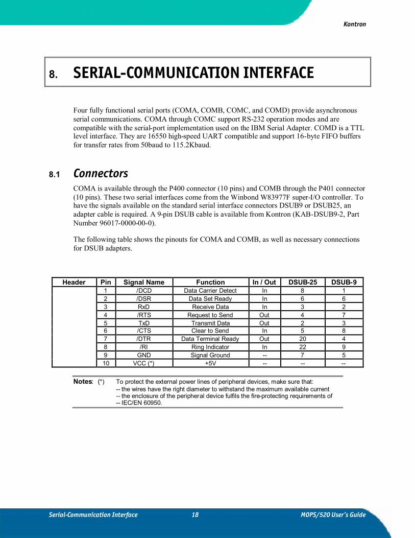
8. SERIAL-COMMUNICATION INTERFACE
Four fully functional serial ports (COMA, COMB, COMC, and COMD) provide asynchronousserial communications. COMA through COMC support RS-232 operation modes and arecompatible with the serial-port implementation used on the IBM Serial Adapter. COMD is a TTLlevel interface. They are 16550 high-speed UART compatible and support 16-byte FIFO buffersfor transfer rates from 50baud to 115.2Kbaud.
8.1 ConnectorsCOMA is available through the P400 connector (10 pins) and COMB through the P401 connector(10 pins). These two serial interfaces come from the Winbond W83977F super-I/O controller. Tohave the signals available on the standard serial interface connectors DSUB9 or DSUB25, anadapter cable is required. A 9-pin DSUB cable is available from Kontron (KAB-DSUB9-2, PartNumber 96017-0000-00-0).
The following table shows the pinouts for COMA and COMB, as well as necessary connectionsfor DSUB adapters.
Header Pin Signal Name Function In / Out DSUB-25 DSUB-91 /DCD Data Carrier Detect In 8 12 /DSR Data Set Ready In 6 63 RxD Receive Data In 3 24 /RTS Request to Send Out 4 75 TxD Transmit Data Out 2 36 /CTS Clear to Send In 5 87 /DTR Data Terminal Ready Out 20 48 /RI Ring Indicator In 22 99 GND Signal Ground -- 7 510 VCC (*) +5V -- -- --
Notes: (*) To protect the external power lines of peripheral devices, make sure that:-- the wires have the right diameter to withstand the maximum available current-- the enclosure of the peripheral device fulfils the fire-protecting requirements of-- IEC/EN 60950.

Kontron
MOPS/520 User’s Guide 19 Serial-Communication Interface
COMC is available through the P403 connector (10 pins in line) COMD is available through theP404 connector (10 pins in line). These two serial interfaces come from the AMD ElanTM SC520microcontroller. To have the signals available on the standard serial interface connectors DSUB9or DSUB25, an adapter cable is required. A 9-pin DSUB cable is available from Kontron (KAB-DSUB9-3, Part Number 96061-0000-00-0).
Header Pin Signal Name Function In / Out DSUB-25 DSUB-91 /DCD Data Carrier Detect In 8 12 /DSR Data Set Ready In 6 63 RxD Receive Data In 3 24 /RTS Request to Send Out 4 75 TxD Transmit Data Out 2 36 /CTS Clear to Send In 5 87 /DTR Data Terminal Ready Out 20 48 /RI Ring Indicator In 22 99 GND Signal Ground -- 7 510 VCC (*) +5V -- -- --
Notes: (*) To protect the external power lines of peripheral devices, make sure that:-- the wires have the right diameter to withstand the maximum available current-- the enclosure of the peripheral device fulfils the fire-protecting requirements of-- IEC/EN 60950.
To find the location of the serial ports on the MOPS/520 board, please see the Appendix E:Connector Layout chapter.
8.2 ConfigurationYou can set the four serial input/output interfaces to a variety of I/O addresses and IRQconfigurations (See the table below). All these settings are changeable from the MOPS/520 BIOSmenu. Refer to the I/O Device Configuration submenu in the Appendix B: BIOS Operationchapter for detailed information on configuration.
Serial Port Possible I/O Addresses Possible IRQsCOMA 3F8h, 2F8h, 3E8h, 2E8h 3, 4, 10COMB 3F8h, 2F8h, 3E8h, 2E8h 3, 4, 11COMC 3F8h 4COMD 2F8 3
Note: Most operating systems detect the serial port with the I/O address 3F8h as COM1and 2F8h as COM2. If COMC and COMD are enabled, the system will detect them asCOM1 and COM2.

Kontron
Serial-Communication Interface 20 MOPS/520 User’s Guide
8.3 LimitationsThe SC520 integrated serial ports (Serial Ports C and D on the MOPS/520) show two deviationsfrom standard UART behavior:
The delta-ring-indicator bit in the modem status register (Bit 2) is only set when thering-indicator signal has changed from an active to an inactive state after the last timethe modem status register was read. Usually this bit is set for RI changes from inactiveto active as well.
In the 16550-compatible mode, a received data interrupt is generated when the veryfirst data byte of a continuous data stream is placed in FIFO. This error only occurs forthe first character of a continuous data stream received by the UART. Following a FIFOtime-out interrupt for the first character received, the remainder of the data streamwill be indicated according to the trigger value set in the RFRT bits of the UART FIFOcontrol registers.
Kontron
MOPS/520 User’s Guide 21 Parallel-Communication Interface
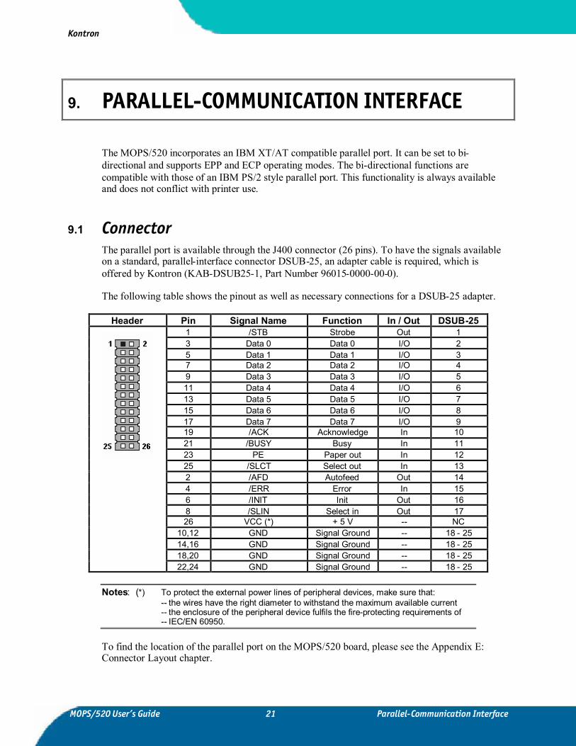
9. PARALLEL-COMMUNICATION INTERFACE
The MOPS/520 incorporates an IBM XT/AT compatible parallel port. It can be set to bi-directional and supports EPP and ECP operating modes. The bi-directional functions arecompatible with those of an IBM PS/2 style parallel port. This functionality is always availableand does not conflict with printer use.
9.1 ConnectorThe parallel port is available through the J400 connector (26 pins). To have the signals availableon a standard, parallel-interface connector DSUB-25, an adapter cable is required, which isoffered by Kontron (KAB-DSUB25-1, Part Number 96015-0000-00-0).
The following table shows the pinout as well as necessary connections for a DSUB-25 adapter.
Header Pin Signal Name Function In / Out DSUB-251 /STB Strobe Out 13 Data 0 Data 0 I/O 25 Data 1 Data 1 I/O 37 Data 2 Data 2 I/O 49 Data 3 Data 3 I/O 511 Data 4 Data 4 I/O 613 Data 5 Data 5 I/O 715 Data 6 Data 6 I/O 817 Data 7 Data 7 I/O 919 /ACK Acknowledge In 1021 /BUSY Busy In 1123 PE Paper out In 1225 /SLCT Select out In 132 /AFD Autofeed Out 144 /ERR Error In 156 /INIT Init Out 168 /SLIN Select in Out 1726 VCC (*) + 5 V -- NC
10,12 GND Signal Ground -- 18 - 2514,16 GND Signal Ground -- 18 - 2518,20 GND Signal Ground -- 18 - 2522,24 GND Signal Ground -- 18 - 25
Notes: (*) To protect the external power lines of peripheral devices, make sure that:-- the wires have the right diameter to withstand the maximum available current-- the enclosure of the peripheral device fulfils the fire-protecting requirements of-- IEC/EN 60950.
To find the location of the parallel port on the MOPS/520 board, please see the Appendix E:Connector Layout chapter.

Kontron
Parallel Communication Interface 22 MOPS/520 User’s Guide
9.2 ConfigurationThe parallel-port mode, I/O addresses, and IRQs are changeable in the MOPS/520 BIOS SetupUtility. You can program the base I/O-address 378h, 3BCh, 278h, disable the interface or set it toAUTO. You can choose IRQ5 or IRQ7 as the parallel-port interrupt. In ECP mode it is possibleto choose DMA 1 or DMA 3.
Refer to the I/O Device Configuration Submenu in the Appendix B: BIOS Operation chapter foradditional information on configuration.
9.3 LimitationsBecause of chipset limitations, parallel-port mode ECP, as well as parallel-port base address3BCh (any mode) cannot be used when a PCI video adapter is installed. The restrictions do notapply if you use ISA video adapters.

Kontron
MOPS/520 User’s Guide 23 Keyboard and Feature Interface
10. KEYBOARD AND FEATURE INTERFACE
The keyboard and feature connector of the MOPS/520 offers five functions. The interfaceconnects the following:
Keyboard
Keyboard lock switch
Speaker
Battery
Reset button
10.1 ConnectorThe keyboard and feature connector is available through Connector P402 (10 pins).
An adapter cable is required to connect a standard keyboard to this interface. There are twoadapter cables available from Kontron:
AT-keyboard (KAB-KB-1, Part Number 96023-0000-00-0)
PS/2-keyboard (KAB-KB-PS2, Part Number 96060-0000-00-0)
The adapter cables do not know the other’s functions on this interface.

Kontron
Keyboard and Feature Interface 24 MOPS/520 User’s Guide
The following table shows the pinout as well as necessary connections for adapters.
Header Pin Signal Name Function 5-pin Din(Diode)
6-pin MiniDin(PS2)
1 Speaker Speaker output2 GND Ground3 /RESIN Reset input4 /KBLOCK Keyboard lock5 KBDAT Keyboard data 2 16 KBCLK Keyboard clock 1 57 GND Ground 4 38 VCC (*) +5V 5 49 BATT Battery in (3,0V)
10 PWRGOOD Powergood
Notes: (*) To protect the external power lines of peripheral devices, make sure that:-- the wires have the right diameter to withstand the maximum available current-- the enclosure of the peripheral device fulfils the fire-protecting requirements of-- IEC/EN 60950.
To find the location of the keyboard and feature connector on the MOPS/520 board, please seethe Appendix E: Connector Layout chapter.

Kontron
MOPS/520 User’s Guide 25 Keyboard and Feature Interface
10.2 ConfigurationRefer to the Keyboard Features submenu in the Appendix B: BIOS chapter for information onconfiguration.
10.3 Signal Descriptions
/KBLOCK (Keyboard Lock)
Input on CPU modules
Output on any other module
Input to the keyboard controller input Port 1, Bit 7
PWRGOOD
Input on CPU modules
When POWERGOOD goes high, it starts the reset generator on the CPU module to pullthe onboard reset line high after a valid reset period. You also can use this pin as a lowactive hardware reset for modules.
/RESIN (Reset input)
Input on CPU modules
When /RESIN is pulled low, the reset generator on the CPU module pulls the onboardreset line low, too and the chipset gets a hardware reset.
Speaker
Open collector output on modules that drive a loudspeaker
Input on modules that connects an 8-Ohm loudspeaker to this pin.
An 8-Ohm loudspeaker is connected between SPEAKER and GND. Connect only oneloudspeaker to this pin. The CPU usually drives this pin. However, other modules alsocan use this signal to drive the system loudspeaker.
KBDAT (Keyboard Data)
Bi-directional I/O pin on CPU modules
Keyboard data signal

Kontron
Keyboard and Feature Interface 26 MOPS/520 User’s Guide
KBCLK (Keyboard Clock)
Bi-directional I/O pin on CPU modules
Keyboard clock signal
VBATT (System Battery Connection)
This pin connects a system battery to all modules.
The battery voltage has to be higher than 2.0V and lower than 3.3V. A 3V battery isrecommended.
A battery is not needed to hold CMOS setup data. Your configurations for hard disks,floppy drives, and other peripherals are saved in an onboard DRAM. However, you needa battery to save the CMOS date and time when power supply is turned off.
10.3.1. Example Connection AT-keyboard and Other Functions
(KBCLK)6 5
(DIN41524)FEMALE
6 PIN MINI-DINFEMALE(PS/2 STYLE)
(+5V Vcc)
(+5V Vcc)(PWRGOOD)
(/KBLOCK)(/RESIN)
(BATT)
(Speaker)
(GND)
(KBDAT)
3
52
1
4
3
5 PIN DIN 180°
124
(KBCLK)(GND)(KBDAT)

Kontron
MOPS/520 User’s Guide 27 PS/2 Mouse Interface
11. PS/2 MOUSE INTERFACE
The super-I/O controller of the MOPS/520 supports a PS/2 mouse.
11.1 ConnectorThe PS/2 mouse interface is available on Connector U406 (4 pins).
An adapter cable is required to connect a standard PS/2 mouse. The cable is available fromKontron (KAB-MOUSE-PS2, Part Number 96062-0000-00-0).
The following table shows the pinout and connections for a PS/2 mouse adapter.
Header Pin Signal Name Function 6-pin MiniDin(PS2)
1 MSDAT Mouse data 12 VCC (*) +5V 43 GND Ground 34 MSCLK Mouse clock 5
Notes: (*) To protect the external power lines of peripheral devices, make sure that:-- the wires have the right diameter to withstand the maximum available current-- the enclosure of the peripheral device fulfils the fire-protecting requirements of-- IEC/EN 60950.
To find the location of the PS/2 mouse connector on the MOPS/520 board, please see theAppendix E: Connector Layout chapter.
11.2 ConfigurationYou can set the PS/2 mouse to enabled, disabled or autodetect from the BIOS Setup. If youenable the mouse, the IRQ12 is used as the interrupt and is no longer available for other devices.Please refer to the Advanced Menu in the Appendix B: BIOS chapter for additional informationon configuration.

Kontron
USB Interface 28 MOPS/520 User’s Guide
12. USB INTERFACE
The MOPS/520 is equipped with a PCI-to-USB bridge Opti 82C861. It comes with two USBports. They follow the OHCI specification and are USB-1.1 compliant. You can expand theamount of USB connections by adding external hubs. You can connect up to 127 USB peripheralsto each hub.
12.1 ConnectorThe USB ports are available through the P1000 and the P1001 connectors (4 pins). To have thesignals available on the standard USB interface connectors, an adapter cable is required. A USBinterface cable is available from Kontron (KAB-USB-1, Part Number 96054-0000-00-0). Thefollowing table shows the pinouts for the USB connector.
Header Pin Signal Name Function1 VCC(*) +5V2 USB0 USB-3 USB1 USB+4 GND Ground
Notes: (*) To protect the external power lines of peripheral devices, make sure that:-- the wires have the right diameter to withstand the maximum available current-- the enclosure of the peripheral device fulfils the fire-protecting requirements of-- IEC/EN 60950.
To find the location of the USB ports on the MOPS/520 board, please see the Appendix E:Connector Layout chapter.
12.2 ConfigurationThere are no configuration entries available for the USB ports in the BIOS Setup Utility.
12.3 LimitationsThe power contacts for USB devices on Pin 1 and Pin 4 are not protected. They are suitable tosupply connected USB devices with a maximum of 500mA power dissipation. Don’t supplyexternal USB devices with a higher power dissipation through this pins. Always use a fuse forpower on external USB connectors, otherwise a defective USB device may damage theMOPS/520.

Kontron
MOPS/520 User’s Guide 29 Floppy-Drive Interface
13. FLOPPY-DRIVE INTERFACE
The floppy-drive interface of the MOPS/520 uses a 2.88MB super I/O floppy-disk controller andcan support one floppy disk drive with densities that range from 360kB to 2.88MB. Thecontroller is 100% IBM compatible.
13.1 ConnectorThe floppy disk interface is available on the flat-foil Connector J401 (26 pins). This type ofconnector is often internally used in notebooks to connect a slim-line floppy drive.
There are different accessories available for this interface from Kontron. To connect a standard3.5” floppy drive, use an adapter cable (ADA-FLOPPY-2, Part Number 96001-0000-00-0). If youhave a slim-line 3.5” floppy drive, you may need a flat foil cable (KAB-FLOPPY/MOPS-1, PartNumber 96019-0000-00-0). It also is possible to get a slim line 3.5” floppy drive with cable fromKontron (FLOPPY-MOPS-1, Part Number 96010-0000-00-0).
The following table shows the connector pinout.
Header Pin Signal Name Function Pin Signal Name Function1 VCC (*) +5V 2 /IDX Index3 VCC (*) +5V 4 /DS0 Drive Select 05 VCC (*) +5V 6 /DCHNG Disk Change7 VCC (*) +5V 8 NC Not connected9 RPM Drive Density 10 /MTR0 Motor on 0
11 NC Not connected 12 /DIR Direction Select13 NC Not connected 14 /Step Step15 GND Ground 16 /WDATA Write Data17 GND Ground 18 /WGATE Write Gate19 GND Ground 20 /TRK0 Track 0021 GND Ground 22 /WRPRT Write Protect23 GND Ground 24 /RDATA Read Data
1
25 GND Ground 26 /CHDSEL Side One Select
Notes: (*) To protect the external power lines of peripheral devices, make sure that:-- the wires have the right diameter to withstand the maximum available current-- the enclosure of the peripheral device fulfils the fire-protecting requirements of-- IEC/EN 60950.
To find the location of floppy-drive interface on the MOPS/520 board, please see the AppendixE: Connector Layout chapter.

Kontron
Floppy-Drive Interface 30 MOPS/520 User’s Guide
13.1.1. Connector Diagram
13.2 ConfigurationYou can configure the floppy disk interface in the BIOS Setup Utility. You can choose the 3.5”(common) or 5.25” drive types with densities of 360kB, 720kB, 1.2MB, 1.25MB, 1.44MB or2.88MB. Refer to the Main Menu section of the Appendix B: BIOS Operation chapter for moreinformation on configuring the floppy drive.
You also can disable the floppy-disk interface in the I/O Device Configuration Submenu.

Kontron
MOPS/520 User’s Guide 31 IDE Interface
14. IDE INTERFACE
The MOPS/520 features one IDE interface that can drive two hard disks. When two devices sharea single adapter they are connected in a master/slave, daisy-chain configuration. If only one driveis in the system, you must set it as the master.
14.1 ConnectorThe IDE interface is available through Connector J300 (44 pins). This interface is designed in2mm grid for optimal connectivity to a 2.5” hard disk.
There are several accessories available for IDE connectivity.
You can use two cables to directly connect a hard disk in a 2.5” form factor (KAB-IDE-2MM,Part Number 96021-0000-00-0) or a 3.5” form factor (KAB-IDE-25, Part Number 96020-0000-00-0).
You can plug a Kontron chipDISK, which is an IDE hard disk that uses Flash technology, into theIDE interface and mechanically mount it by using a mini-spacer on the chipDISK hole. You alsocan use a chipDISK adapter (chipDISK-ADA1, Part Number 96004-0000-00-0) or compact Flashadapter (CFC-ADA1, Part Number 96004-0000-00-2) for more disk support.

Kontron
IDE Interface 32 MOPS/520 User’s Guide
The following table shows the pinout.
Header Pin Signal Name Function Pin Signal Name Function1 /RESET Reset 2 GND Ground3 HDD7 Data 7 4 HDD8 Data 85 HDD6 Data 6 6 HDD9 Data 97 HDD5 Data 5 8 HDD10 Data 109 HDD4 Data 4 10 HDD11 Data 11
11 HDD3 Data 3 12 HDD12 Data 1213 HDD2 Data 2 14 HDD13 Data 1315 HDD1 Data 1 16 HDD14 Data 1417 HDD0 Data 0 18 HDD15 Data 1519 GND Ground 20 Key (NC) Key pin21 NC Not connected 22 GND Ground23 /IOW I/O write 24 GND Ground25 /IOR I/O read 26 GND Ground27 IOCHRDY I/O channel ready 28 RES Reserved29 NC Not connected 30 GND Ground31 IRQ14 Interrupt 32 /IOCS16 16bit I/O33 SA1 Addr 1 34 NC Not connected35 SA0 Addr 0 36 SA2 Addr 237 /CS0 Chip select 0 38 CS1 Chip select 139 NC Not connected 40 GND Ground41 VCC (*) +5V 42 VCC (Motor) +5V43 GND Ground 44 NC Not connected
Notes: (*) To protect the external power lines of peripheral devices, make sure that:-- the wires have the right diameter to withstand the maximum available current-- the enclosure of the peripheral device fulfils the fire-protecting requirements of-- IEC/EN 60950.
To find the location of IDE-controller interface on the MOPS/520 board, please see the AppendixE: Connector Layout chapter.
14.2 ConfigurationThe IDE interface offers several configuration settings. Refer to the Main Menu and I/O DeviceConfiguration Submenu in the Appendix B: BIOS Operation chapter for additional informationon configuration.

Kontron
MOPS/520 User’s Guide 33 Ethernet Interface
15. ETHERNET INTERFACE
The MOPS/520 uses the Davicom DM9102A PCI Fast Ethernet Controller. The networkcontroller supports a 10/100Base-T interface. The device auto-negotiates the use of a 10Mbit/secor 100Mbit/sec connection. You can enable an onboard LAN RPL ROM to support the boot up ofthe system via Ethernet and a PXE-boot server.
The Davicom DM9102A provides the following features:
Integrated Fast Ethernet MAC, Physical Layer, and transceiver on one chip
Compliance with PCI Specification 2.2
PCI-bus-master architecture
EEPROM 93C46 interface supports node ID, access-configuration information
Compliance with IEEE 802.3u 100Base-TX and 802.3 10Base-T
Compliance with IEEE 802.3u autonegotiation protocol for automatic link- typeselection
Full-duplex/half-duplex capability
Support IEEE 802.3x Full Duplex Flow Control
Digital clock recovery circuit using advanced digital algorithm to reduce jitter
High-performance 100Mbps clock generator and data-recovery circuit
Loopback mode for easy system diagnostics
Note: The Ethernet interface works according to the common criteria of the embeddedtechnology market segment.
15.1 ConnectorThe Ethernet interface is available through Connector X700 (8 pins).
To have the signals of the Ethernet connection available on a standard RJ45 connector, you needan adapter cable, which is offered by Kontron (KAB-MOPS-ETN1, Part Nr 96048-0000-00-0).

Kontron
Ethernet Interface 34 MOPS/520 User’s Guide
The following table shows the pinout.
Header Pin Signal Name Function In/Out1 TXD+ 10BASE-T Transmit Differential Output2 TXD- 10BASE-T Transmit Differential Output3 RXD+ 10BASE-T Receive Differential Input4 SHLDGND Shield ground5 SHLDGND Shield ground6 RXD- 10BASE-T Receive Differential Input7 SHLDGND Shield ground8 SHLDGND Shield ground
Notes: TXD+, TXD- differential-output pair drives 10 and 100Mb/s Manchester-encodeddata to 100/10BASE-T transmit lines.RXD+, RXD- differential input pair receives 10 and 100Mb/s Manchester-encodeddata from 100/10BASE-T receive lines.
To find the location of the Ethernet interface on the MOPS/520 board, please see the Appendix E:Connector Layout chapter.
15.2 ConfigurationThe onboard Davicom DM9102A Ethernet controller can be enabled or disabled in BIOS setuputility. Refer to the I/O Device Configuration Submenu in the Appendix B: BIOS Operationchapter for additional information on configuration.
You can download available drivers from the Kontron Web site. For further information read theread-me file or contact technical support.
15.3 Ethernet Technical SupportIf any problems occur, you can solve some of them by using the latest drivers for the DavicomDM9102A controller. Kontron provides you with the latest in house- tested drivers, which candiffer from newer ones. For further technical support, contact either Kontron or get supportinformation and downloadable software updates from Davicom.

Kontron
MOPS/520 User’s Guide 35 Power Connection
16. POWER CONNECTION
In some applications, the MOPS/520 is intended for use as a stand-alone module without abackplane. You need to have a power connector available on the board for direct power supply.The MOPS/520 is a +5V-only board. Peripherals can obtain additional voltage from the powerconnector next to the PC/104 bus. The additional voltages (+12V, -5V and -12V) are notgenerated onboard the MOPS/520A.
The +3.3V for PC/104-Plus boards are also not generated on the MOPS/520 board. You mustsupply PC/104-Plus boards separately through the PC/104-Plus bus. Use +5V PC/104-Plus add-on cards.
16.1 ConnectorThe power connector is available as P800C (8 pins).
The following table shows the pinout.
Header Pin Signal Name Function1 GND Ground2 +5V +5V3 VBATT Battery4 +12V +12V5 -5V -5V6 -12V -12V7 GND Ground
1 2
8
8 VCC +5V
To find the location of the power connector on the MOPS/520 board, please see the Appendix E:Connector Layout chapter.

Kontron
Power Connection 36 MOPS/520 User’s Guide
16.2 Power PinsEvery power pin on the power connector as well as on the PC/104 and PC/104-Plus busconnectors is limited to a maximum current of 1A per pin.
If a system using a MOPS/520 is only supplied from the power connector, the followinglimitations apply:
Power Number of Pins Max. CurrentVCC (+5V) 2 2A
+12V 1 1A-12V 1 1A-5V 1 1A
GND 2 2A
A system using the MOPS/520 also can be supplied from the PC/104 and PC/104-Plus busconnectors. If only those supply voltages pins are used, the following limitations apply:
Power Number of pins onISA part
Number of pins onPCI part
Max. Current
VCC (+5V) 4 8 4A + 8A = 12A+12V 2 1 2A + 1A = 3A-12V 2 1 2A + 1A = 3A-5V 2 0 2A
+3.3V 0 10 10AGND 8 23 8A + 23A = 31A
Modules on the PC/104 bus or PC/104-Plus bus consuming a higher supply current must providepower supply through an additional connector.
Note: The MOPS/520 is not a replacement for a backplane. Use all power pins on thepower connector and on the PC/104 connectors for power supply to theMOPS/520, and also use all additional power connectors on additional I/O cards,if your system exceeds the above limitations. It is not acceptable to use only thepower pins of the PC/104 connector for power supply of the full PC/104 stack.

Kontron
MOPS/520 User’s Guide 37 Power Connection
16.3 External BatteryYou can connect an external battery to Pin 3 (VBATT) of the power connector instead of Pin 9 ofthe KBD connector.
Note: The two battery inputs are protected against each other by diodes.

Kontron
CAN Controller Interface 38 MOPS/520 User’s Guide
17. CAN CONTROLLER INTERFACE (OPTIONAL)
The MOPS/520 board can be equipped with an Intel 82527 CAN controller. The frequency of thedata rate for the CAN bus is 8MHz.
The 82527 serial-communications controller performs serial communication, following the CANprotocol. The controller, with minimal interaction from the host microcontroller or CPU,performs all serial-communication functions such as:
Transmitting and receiving messages
Filtering messages
Transmitting searches
Interrupting searches
The Philips PCA82C251 CAN transceiver for 24V systems serves as the interface between theCAN protocol controller and the physical bus.
17.1 ConnectorThe CAN interface is available through Connector U1200 (4 pins).
Header Pin Signal Name Function1 CAN_L Low level CAN voltage I/O2 CAN_H High Level CAN voltage I/O3 VCC (*) +5V4 GND Ground
Notes: (*) To protect the external power lines of peripheral devices, make sure that:-- the wires have the right diameter to withstand the maximum available current-- the enclosure of the peripheral device fulfils the fire-protecting requirements of-- IEC/EN 60950.
On the MOPS/520 board, the CAN bus terminates with two resistors of 120 Ohm in parallelacross CAN_L and CAN_H. This single, 60-Ohm termination scheme is chosen to simplify CANhookups with short bus lengths. Depending on the network topology employed and the total buslength, a modified termination network may be desirable in some applications. Under thosecircumstances, contact Kontron technical support for assistance.

Kontron
MOPS/520 User’s Guide 39 CAN Controller Interface
17.2 ConfigurationThe CAN controller can be configured in the BIOS setup utility. You can enable/disable the CANcontroller, choose a base I/O address location between 400hex and 2000hex and an interruptIRQ5/IRQ9. Refer to the I/O Device Configuration Submenu in the Appendix B: BIOS chapterfor information on configuration.
The I/O base address selects a range of 256 bytes in the I/O-address space, where theconfiguration registers of the CAN controllers are mapped. There are no special drivers availablefor the CAN controller. You must program the CAN controller using this address space. Refer tothe datasheets of the Intel 82527 controller for details about the configuration registers and theirprogramming. Information about those details would exceed the capabilities of this document.

Kontron
Watchdog Timer 40 MOPS/520 User’s Guide
18. WATCHDOG TIMER
The watchdog timer is integrated in the chipset of the MOPS/520 and can issue a reset to thesystem or generate a nonmaskable interrupt (NMI). The watchdog timer circuit has to betriggered within a specified time by the application software. If the watchdog is not triggeredbecause proper software execution fails or a hardware malfunction occurs, it will reset the systemor generate the NMI.
18.1 ConfigurationYou can set the watchdog timer to disabled, reset or NMI mode. You can specify the delay timeand timeout (trigger period) from 0.5 seconds up to 32 seconds. The delay time is the time afterfirst initialization before the trigger period starts. The timeout is the time the watchdog has to betriggered within. You can make the initialization settings in the BIOS setup. Refer to theWatchdog Settings Submenu in the Appendix B: BIOS Operation chapter for information onconfiguration.
18.2 Programming
18.2.1. InitializationYou can initialize the watchdog timer from the BIOS setup, the application software, using low-level programming or with help of the JIDA (Jumptec Intelligent Device Architecture)programmer’s interface.
18.2.2. TriggerThe watchdog needs to be triggered out of the application software within the specified timeoutperiod. You can only do this in the application software by using low-level programming or withhelp of the JIDA (Jumptec Intelligent Device Architecture) programmer’s interface.
For information about low-level programming for the watchdog timer, refer to Application NoteWdogP489_E???.DOC, which you can request from Kontron technical support.
For information about the JIDA programmer’s interface refer to the JIDA BIOS extension sectionin the Appendix B: BIOS chapter and separate documents available in the JIDA softwarepackages on the Kontron Web site.

Kontron
MOPS/520 User’s Guide 41 Appendix A: System Resource Allocations
19. APPENDIX A: SYSTEM RESOURCEALLOCATIONS
19.1 Interrupt Request (IRQ) LinesPlease note that Kontron PC/104 devices were designed after the draft of P996 Specification forISA systems. Because of this, shareable interrupts are not supported. Some PC/104 add-on boardmanufacturers do not follow the P996 Specification and allow shareable interrupts. If you want touse such PC/104 boards with Kontron devices, contact the manufacturer of the add-on board andask about switching to non-interrupt sharing.
IRQ # Use Available Comment0 Timer0 No1 Keyboard No2 Cascade No3 COM2 No Note (1), Note (2)4 COM1 No Note (1), Note (2)5 CAN-Bus No Note (1), Note (3), Note (4)6 FDC No Note (1)7 LPT1 No Note (1), Note (3)8 RTC No9 Yes Note (4)10 COM3 No Note (1), Note (2)11 COM4 No Note (1), Note (2)12 PS/2 Mouse No Note (1)13 FPU No14 IDE0 No Note (1)15 No Not available on the PC/104 bus with MOPS/520
Notes:(1) If the „used for“ device is disabled in setup, the corresponding interrupt is available forother devices.
(2) ATTENTION: BIOS settings determine which physical COM connector is assigned toa logical COM port.
(3) LPT1 also can be configured for IRQ5 (avoid conflict with the CAN controller bychanging its interrupt).
(4) Users can assign the CAN controller IRQ9 if needed.

Kontron
Appendix A: System Resource Allocations 42 MOPS/520 User’s Guide
19.2 Direct Memory Access (DMA) Channels
DMA # Use Available Comment0 No Not available on PC/104 bus with MOPS/5201 Yes Note (2)2 FDC No Note (1)3 LPT1 No Note (3)4 Cascade No Not available5 Yes6 No Not available on PC/104 bus with MOPS/5207 No Not available on PC/104 bus with MOPS/520
Notes:(1) If the Used For device is disabled in setup, the corresponding DMA channel isavailable for other devices.
(2) LPT1 also can be configured for DMA Channel #1.
(3) The DMA channel is only used in ECP mode; it is free in other modes.

Kontron
MOPS/520 User’s Guide 43 Appendix A: System Resource Allocations
19.3 Memory MapThe MOPS/520 processor module can come with up to 64MB of memory. The first 640KB ofDRAM are used as main memory.
Using DOS, you can address 1MB of memory directly. Memory area above 1MB (high memory,extended memory) is accessed under DOS via special drivers such as HIMEM.SYS andEMM386.EXE, which are part of the operating system. Please refer to the operating systemdocumentation or special textbooks for information about HIMEM.SYS and EMM386.EXE.
Other operating systems (Linux or Windows versions) allow you to address the full memory areadirectly.
Upper Memory Use Available CommentA0000h – BFFFFh VGA Memory No Mainly used by graphic adapter cards. If PCI
graphic card is in the system this memory area ismapped to PCI bus.
C0000h – C7FFFh VGA BIOS Yes Free for ISA bus or shadow RAM in standardconfiguration, mainly used by graphic adaptercards!
C8000h – DFFFFh Yes Free for ISA bus or shadow RAM in standardconfiguration.If onboard LAN RPL ROM is enabled, JRC is usedor alphanumeric LCD support is enabled; a 32Kblock is shadowed for BIOS extensions, startingwith first free area at C8000h or D0000h or D8000h.(BIOS extensions do not use the whole shadowblock.)
E0000h – F0000h System BIOS No

Kontron
Appendix A: System Resource Allocations 44 MOPS/520 User’s Guide
19.3.1. Using Expanded Memory ManagersMOPS/520 extension BIOSes may be mapped to an upper memory area. (See the previoustable.). Some add-on boards also have optional ROMs or use drivers that communicate with theircorresponding devices via memory mapped I/O such as dual-ported RAM. These boards have toshare the upper memory area with the Expanded Memory Manager’s EMS frame. This oftencauses several problems in the system.
Most EMMs scan the upper memory area for extension BIOSes (optional ROMs) and choose afree memory area for their frame if it is not explicitly set. Normally, they are not always capableof detecting special memory-mapped I/O areas. You need to tell the EMM which memory areasare not available for the EMS frames, which is most of the time done by using special exclusionparameters.
If the Expanded Memory Manager you use cannot detect extension BIOSes (optional ROMs),make sure you excluded all areas in the upper memory, which are used by extension BIOSes, too.Your instruction in the CONFIG.SYS concerning the Expanded Memory Manager should looklike this: (question marks for location of extension BIOS).
MS-DOS Example:DEVICE=EMM386.EXE X=????-???? X=E000-FFFF
Note: When booting up your system using this configuration under MS-DOS, theexclusion of area F000 to FFFF causes a warning. Microsoft reports that thismessage will always appear when the F000 segment lies in the shadow RAM.This is a bug of EMM386, not of the MOPS/520.
Please carefully read the technical manuals of add-on cards used with the MOPS/520 for thememory areas they use. If necessary, also exclude their memory locations to avoid a conflict withthe EMM.

Kontron
MOPS/520 User’s Guide 45 Appendix A: System Resource Allocations
19.4 I/O Address MapThe I/O-port addresses of the processor module MOPS/520 are functionally identical to astandard PC/AT. All addresses not mentioned in this table should be available. We recommendthat you do not use I/O addresses below 0110hex with additional hardware for compatibilityreasons, even if they are available on the MOPS/520.
I/O Addresses Use Available Comment0000-000Fh Slave DMA Controller No Fixed
0010h SC520 chipset No Fixed0020-0026h Interrupt Controller 1 No Fixed0040-0043h Counter/timer No Fixed
0044 SC520 chipset No Fixed0060-0065h Keyboard controller No Fixed0070-0071h Real-time clock No Fixed
0072h SC520 chipset No Fixed0080-008Fh DMA page register 74LS612 No Fixed0090-0094h System Control + Fast A20 Gate No Fixed00A0-00A2h Interrupt Controller 2 No Fixed00C0-00DFh DMA Controller 2 No Fixed
00E1h System Control No Fixed00F0h Floating Point Error Int. Clear No Fixed
0100-0103h Onboard GPIO port No Fixed01F0-01F8h Fixed disk No Fixed0278-027Fh Parallel Port 2 Yes Free in standard configuration, but
possible address of LPT.02E8-02EFh User specific Serial Port (COM4) Yes Free in standard configuration, but
possible address of COM.02F8-02FFh Serial Port 2 No Default for COM B, free with different
configuration.0370-0377h Configuration Port No Configuration address for Winbond-
controller.0378-037Fh Parallel Port 1 No Default for LPT 1; free with different
configuration.03BC-03C4h User-specific Parallel Port Yes Free in standard configuration but
possible address of LPT.03E8-03Efh User-specific Serial Port (COM3) Yes Free in standard configuration, but
possible address of COM.03F0-03F7h Diskette controller No Fixed.03F8-03FFh Serial Port 1 No Default for COM A; free if different
configuration used.0400-04FFh Yes Free in standard configuration but
possible address of CAN1000-107Fh Ethernet Controller No Free if Ethernet Controller is disabled1000-10FFh Yes Free in standard configuration but
possible address of CAN1600-16FFh Yes Free in standard configuration but
possible address of CAN2000-20FFh No Default address range of CAN controller
Note: The MOPS/520 only maps addresses up to 03FFhex to the ISA bus. All higheraddresses are by default mapped to the PCI bus. You can map additional ISA I/Oareas to the ISA bus in the BIOS setup. See I/O Device Configuration submenuin the BIOS chapter Appendix B: for details.

Kontron
Appendix A: System Resource Allocations 46 MOPS/520 User’s Guide
19.5 Peripheral Component Interconnect (PCI) DevicesAll devices follow the PCI 2.1 specification. The BIOS and OS control memory and I/Oresources. Please refer to the PCI 2.1 specification for details.
PCI Device (IDSEL) PCI IRQ REQ/ GNT CommentEthernet (AD12) INTB# REQ3#/GNT3# PC/104plus specification allows
only 3 external masters:(REQ0, REQ1, REQ2)
USB Controller (AD13) INTC# REQ4#/GNT4# PC/104plus specification allowsonly 3 external masters:(REQ0, REQ1, REQ2)
Kontron
MOPS/520 User’s Guide 47 Appendix B: BIOS Operation
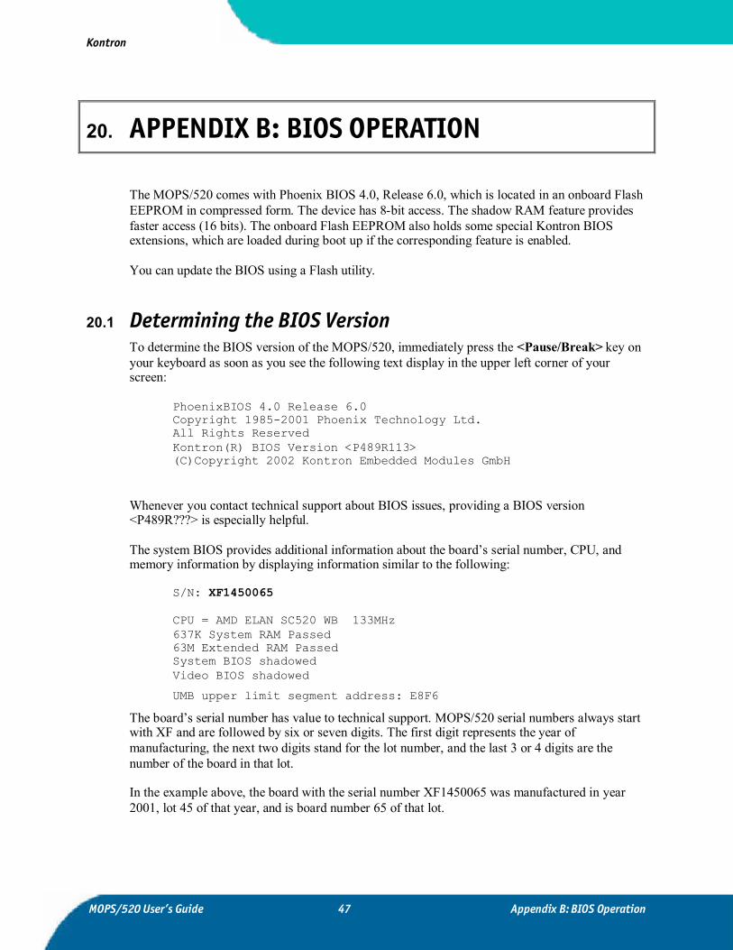
20. APPENDIX B: BIOS OPERATION
The MOPS/520 comes with Phoenix BIOS 4.0, Release 6.0, which is located in an onboard FlashEEPROM in compressed form. The device has 8-bit access. The shadow RAM feature providesfaster access (16 bits). The onboard Flash EEPROM also holds some special Kontron BIOSextensions, which are loaded during boot up if the corresponding feature is enabled.
You can update the BIOS using a Flash utility.
20.1 Determining the BIOS VersionTo determine the BIOS version of the MOPS/520, immediately press the <Pause/Break> key onyour keyboard as soon as you see the following text display in the upper left corner of yourscreen:
PhoenixBIOS 4.0 Release 6.0Copyright 1985-2001 Phoenix Technology Ltd.All Rights ReservedKontron(R) BIOS Version <P489R113>(C)Copyright 2002 Kontron Embedded Modules GmbH
Whenever you contact technical support about BIOS issues, providing a BIOS version<P489R???> is especially helpful.
The system BIOS provides additional information about the board’s serial number, CPU, andmemory information by displaying information similar to the following:
S/N: XF1450065
CPU = AMD ELAN SC520 WB 133MHz637K System RAM Passed63M Extended RAM PassedSystem BIOS shadowedVideo BIOS shadowed
UMB upper limit segment address: E8F6
The board’s serial number has value to technical support. MOPS/520 serial numbers always startwith XF and are followed by six or seven digits. The first digit represents the year ofmanufacturing, the next two digits stand for the lot number, and the last 3 or 4 digits are thenumber of the board in that lot.
In the example above, the board with the serial number XF1450065 was manufactured in year2001, lot 45 of that year, and is board number 65 of that lot.
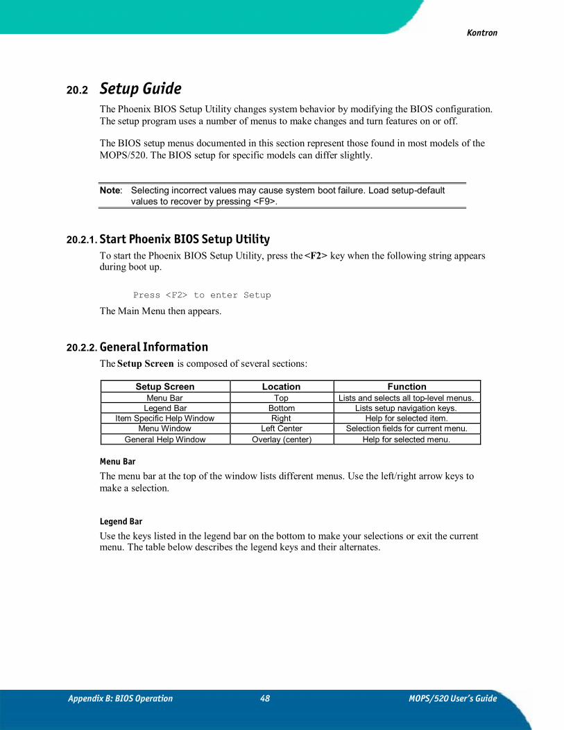
Kontron
Appendix B: BIOS Operation 48 MOPS/520 User’s Guide
20.2 Setup GuideThe Phoenix BIOS Setup Utility changes system behavior by modifying the BIOS configuration.The setup program uses a number of menus to make changes and turn features on or off.
The BIOS setup menus documented in this section represent those found in most models of theMOPS/520. The BIOS setup for specific models can differ slightly.
Note: Selecting incorrect values may cause system boot failure. Load setup-defaultvalues to recover by pressing <F9>.
20.2.1. Start Phoenix BIOS Setup UtilityTo start the Phoenix BIOS Setup Utility, press the <F2> key when the following string appearsduring boot up.
Press <F2> to enter Setup
The Main Menu then appears.
20.2.2. General InformationThe Setup Screen is composed of several sections:
Setup Screen Location FunctionMenu Bar Top Lists and selects all top-level menus.
Legend Bar Bottom Lists setup navigation keys.Item Specific Help Window Right Help for selected item.
Menu Window Left Center Selection fields for current menu.General Help Window Overlay (center) Help for selected menu.
Menu Bar
The menu bar at the top of the window lists different menus. Use the left/right arrow keys tomake a selection.
Legend Bar
Use the keys listed in the legend bar on the bottom to make your selections or exit the currentmenu. The table below describes the legend keys and their alternates.

Kontron
MOPS/520 User’s Guide 49 Appendix B: BIOS Operation
Key Function<F1> or <Alt-H> General Help window.
<Esc> Exit menu. or Arrow key Select a menu.or Arrow key Select fields in current menu.
<Tab> or <Shift-Tab> Cycle cursor up and down.<Home> or <End> Move cursor to top or bottom of current window.
<PgUp> or <PgDn> Move cursor to next or previous page.<F5> or <-> Select previous value for the current field.
<F6> or <+> or <Space> Select next value for the current field.<F9> Load the default configuration values for this menu.<F10> Save and exit.
<Enter> Execute command or select submenu.<Alt-R> Refresh screen.
Selecting an ItemUse theor key to move the cursor to the field you want. Then use the + and - keys to select avalue for that field. The Save Value commands in the Exit menu save the values displayed in allthe menus.
Displaying Submenus
Use the or key to move the cursor to the submenu you want. Then press <Enter>. Apointer () marks all submenus.
Item Specific Help Window
The Help window on the right side of each menu displays the Help text for the selected item. Itupdates as you move the cursor to each field.
General Help WindowPressing <F1> or <Alt-F1> on a menu brings up the General Help window that describes thelegend keys and their alternates. Press <Esc> to exit the General Help window.

Kontron
Appendix B: BIOS Operation 50 MOPS/520 User’s Guide
20.3 Main MenuFeature Option Description
System Time HH:MM:SS Set system time. Press <Enter> to move to MM or SS.System Date MM/DD/YYYY Set system date. Press <Enter> to move to DD or YYYY.
Legacy Diskette A 360 kB, 5 ¼”1.2 MB, 5 ¼”720 kB, 3 ½”
1.44/1.25 MB, 3 ½”2.88 MB, 3 ½”Not installed
Disabled
Select type of installed floppy disk drive.
Primary Master Autodetected drive Displays results of PM autotyping.Primary Slave Autodetected drive Displays results of PS autotyping.Memory Shadow Submenu Opens Memory Shadow submenu.System Memory N/A Displays amount of conventional memory detected during bootup.
Extended Memory N/A Displays amount of extended memory detected during bootup.
Note: In the Option column, bold shows default settings.

Kontron
MOPS/520 User’s Guide 51 Appendix B: BIOS Operation
20.3.1. Master or Slave Submenus
Feature Option DescriptionType None
UserAuto
CD-ROM
None = Autotyping is not able to supply the drive type or end userhas selected None, disabling any drive that may be installed.
User = End user supplies the hdd information.Auto = Autotyping, the drive itself supplies the information.
CD-ROM = CD-ROM drive.Cylinders 1 to 65,536 Number of cylinders in CHS format.
Heads 1 to 256 Number of read/write heads in CHS format.Sectors 1 to 63 Number of sectors per track in CHS format.
Maximum Capacity N/A Displays the calculated size of the drive using CHS format.Total Sectors* N/A Total number of sectors in LBA mode as reported by the drive
during autotyping.Maximum Capacity N/A Displays the calculated size of the drive by using the LBA format.
Multi-Sector Transfers DisabledStandard2 sectors4 sectors8 sectors
16 sectors
Any selection except Disabled determines the number of sectorstransferred per block.
The standard is 1 sector per block.
LBA Mode Control DisabledEnabled
Enabling LBA uses Logical Block Addressing instead of CHS.
Notes: In the Option column, bold shows default settings.(*) Only if LBA Mode Control is enabled.
20.3.2. Memory Shadow Submenu
Feature Option DescriptionVideo Shadow Disabled
EnabledEnables/disables shadowing of video ROM.
C8000 – CFFFF DisabledEnabled
Accesses to this upper memory region go to the ISA bus if Disabled or tolocal memory if Enabled.
This option does not display if VGA BIOS exceeds 32KB. In that case,the region is shadowed automatically.
D0000 – D7FFF DisabledEnabled
Accesses to this upper memory region go to the ISA bus if Disabled or tolocal memory if Enabled.
D8000 – DFFFF DisabledEnabled
Accesses to this upper memory region go to the ISA bus if Disabled or tolocal memory if Enabled.
Note: In the Option column, bold shows default settings.

Kontron
Appendix B: BIOS Operation 52 MOPS/520 User’s Guide
20.4 Advanced MenuAll entries in this part of the BIOS setup utility are very vital to your system. Only changesettings when you are sure, what you are doing. Some changes may not be suitable for yourcomplete system and may lead to unwanted system behavior.
Feature Option DescriptionAdvanced Chipset Control Submenu Opens Advanced Chipset Control submenu.PCI Configuration Submenu Opens PCI Configuration submenu.
PNP OS installed YesNo
If your system has a PNP OS (such as Win98)select Yes to let the OS configure PNP devices
not required for boot. No makes the BIOSconfigure them.
Reset Configuration Data NoYes
Yes erases all configuration data in ESCD,which stores the configuration settings for plug-in devices. Select Yes when required to restore
the manufacturer’s defaults.PS/2 Mouse Disabled
EnabledAuto Detect
Disables or enables PS/2 mouse.Auto Detect enables PS/2 mouse if BIOS
detects one.Keyboard Features Submenu Opens Keyboard Features submenu.
I/O Device Configuration Submenu Opens I/O Device Configuration submenu.Large Disk Access Mode DOS
OtherSelect DOS if you have DOS. Select Other if
you have another OS such as UNIX.A large disk is one that has more than 1024
cylinders, more than 16 heads or more than 63sectors per track.
Halt On Errors YesNo
Determines if post errors cause system to halt.
Note: In the Option column, bold shows default settings.

Kontron
MOPS/520 User’s Guide 53 Appendix B: BIOS Operation
20.4.1. Advanced Chipset Control Submenu
Feature Option DescriptionCPU Speed 100 MHz
133 MHzSelect internal CPU frequency. 100MHz slows
performance and also decreases power consumption.Cache Mode Write Back
Write ThroughSelect SC520 L1 cache mode.
CAS latency 3T2T
Select CAS latency. Lower value speeds up SDRAMaccesses.
RAS to CAS delay 2T3T4T
Select RAS to CAS delay. Lower values speed upSDRAM accesses.
RAS Precharge time 2T3T4T6T
Select RAS precharge time. Lower values speed upSDRAM accesses.
Refresh cycle time 7.8 us15.6 us31.2 us62.5 us
Select SDRAM refresh cycle time. Higher valuesspeed up SDRAM accesses.
SDRAM buffer DisabledEnabled
The integrated SDRAM read/write buffer increasesoverall system performance.
ISA bus cycle duration: 400ns800NS1.2us2us
Set duration of complete ISA bus cycle. The onboardcomponents function with all values, but ISA add-on
cards as well as IDE hard disks may require slower orfaster ISA accesses.
Note: In the Option column, bold shows default settings.

Kontron
Appendix B: BIOS Operation 54 MOPS/520 User’s Guide
20.4.2. PCI Configuration SubmenuFeature Option Description
PCI concurrent mode DisabledEnabled
In concurrent mode, direct PCI-to-PCI transfers do notrequire gaining ownership of the CPU-memory host
bus. Thus PCI transfers are accelerated. If you have aPCI add-on card that doesn’t allow direct PCI-to-PCI
transfers set to disabled.Park PCI on CPU* Enabled
DisabledEnabled: The PCI bus is parked on the CPU after a
PCI transaction.Disabled: The PCI bus is parked on last PCI master.
CPU PCI masterpriority*
1, 2, 3 The CPU is granted the PCI bus after the selectednumber of external PCI master cycles.
Delay Transaction* DisabledEnabled
Enabled maximizes PCI bus efficiency by freeing upthe bus while initial SDRAM read is issued.
Host-PCI Write Buffer* DisabledEnabled
Maximizes host-write accesses to PCI.
PCI Device, Slot #1 Submenu Opens submenu to configure slot 1 PCI device.PCI Device, Slot #2 Submenu Opens submenu to configure slot 2 PCI device.PCI Device, Slot #3 Submenu Opens submenu to configure slot 3 PCI device.PCI Device, Slot #4 Submenu Opens submenu to configure slot 4 PCI device.
PCI IRQ line 1 DisabledAuto Select
IRQ3, 4, 5, 7, 9,10, 11, 12,
14,15
Select IRQ for PIC interrupt INTA.Select ‘Auto’ to allow BIOS to assign the IRQ.
PCI IRQ line 2 DisabledAuto Select
IRQ3, 4, 5, 7, 9,10, 11, 12,
14,15
Select IRQ for PIC interrupt INTB.Select Auto to let the BIOS assign the IRQ.
PCI IRQ line 3 DisabledAuto Select
IRQ3, 4, 5, 7, 9,10, 11, 12,
14,15
Select IRQ for PIC interrupt INTC.Select Auto to let the BIOS assign the IRQ.
PCI IRQ line 4 DisabledAuto Select
IRQ3, 4, 5, 7, 9,10, 11, 12,
14,15
Select IRQ for PIC interrupt INTD.Select Auto to let the BIOS assign the IRQ.
PCI/PNP ISA UMBRegion Exclusion
Submenu Opens UMB Region Exclusion submenu.
PCI/PNP ISA IRQResource Exclusion
Submenu Opens IRQ Exclusion submenu.
Assign IRQ to PCI VGA YesNo
Most graphic cards do not need an IRQ assigned.However, Win98 2nd Edition does not work properly if
an IRQ is not assigned.
Note: In the Option column, bold shows default settings.(*) This setting is only visible if the PCI concurrent mode is set to Enabled.

Kontron
MOPS/520 User’s Guide 55 Appendix B: BIOS Operation
20.4.3. PCI Device, Slot #X Submenu
Feature Option DescriptionOption ROM Scan Disabled
EnabledInitialize device expansion ROM.
Enable Master DisabledEnabled
Enables device in slot as a PCI bus master. Not everydevice can function as a master. Check your device
documentation.Latency Timer 20h, 40h, 60h,
80h, A0h, C0h,E0h
Minimum guaranteed time slice allocated for busmaster in units of PCI bus clocks.
A high-priority, high-throughput device may benefitfrom a greater value.
Note: In the Option column, bold shows default settings.
20.4.4. PCI/PNP ISA UMB Region Exclusion Submenu
Feature Option DescriptionC800 - CBFF Available
ReservedReserves the specified block of upper memory for use
by legacy ISA devices.CC00 - CFFF Available
ReservedReserves the specified block of upper memory for use
by legacy ISA devices.D000 – D3FF Available
ReservedReserves the specified block of upper memory for use
by legacy ISA devices.D400 – D7FF Available
ReservedReserves the specified block of upper memory for use
by legacy ISA devices.D800 - DBFF Available
ReservedReserves the specified block of upper memory for use
by legacy ISA devices.DC00 - DFFF Available
ReservedReserves the specified block of upper memory for use
by legacy ISA devices.
Note: In the Option column, bold shows default settings.

Kontron
Appendix B: BIOS Operation 56 MOPS/520 User’s Guide
20.4.5. PCI/PNP ISA IRQ Exclusion Submenu
Feature Option DescriptionC800 - CBFF Available
ReservedReserves the specified block of upper memory for use
by legacy ISA devices.CC00 - CFFF Available
ReservedReserves the specified block of upper memory for use
by legacy ISA devices.D000 – D3FF Available
ReservedReserves the specified block of upper memory for use
by legacy ISA devices.D400 – D7FF Available
ReservedReserves the specified block of upper memory for use
by legacy ISA devices.D800 - DBFF Available
ReservedReserves the specified block of upper memory for use
by legacy ISA devices.DC00 - DFFF Available
ReservedReserves the specified block of upper memory for use
by legacy ISA devices.
Note: In the Option column, bold shows default settings.
20.4.6. PCI/PNP ISA IRQ Exclusion Submenu
Feature Option DescriptionIRQ3 Available
ReservedReserves specified IRQ for use by legacy ISA devices.
IRQ4 AvailableReserved
Reserves specified IRQ for use by legacy ISA devices.
IRQ5 AvailableReserved
Reserves specified IRQ for use by legacy ISA devices.
IRQ7 AvailableReserved
Reserves specified IRQ for use by legacy ISA devices.
IRQ9 AvailableReserved
Reserves specified IRQ for use by legacy ISA devices.
IRQ10 AvailableReserved
Reserves specified IRQ for use by legacy ISA devices.
IRQ11 AvailableReserved
Reserves specified IRQ for use by legacy ISA devices.
IRQ15 AvailableReserved
Reserves specified IRQ for use by legacy ISA devices.
Note: In the Option column, bold shows default settings.

Kontron
MOPS/520 User’s Guide 57 Appendix B: BIOS Operation
20.4.7. Keyboard Features Submenu
Feature Option DescriptionNumLock Auto
OnOff
‘On’ or ‘Off’ turns NumLock on or off at bootup. Autoturns NumLock on if it finds a numeric keypad.
Key Click DisabledEnabled
Turns audible key click on.
Keyboard auto-repeatrate
30/sec, 26.7/sec,21.8/sec, 18,5/sec,13.3/sec, 10/sec,
6/sec, 2/sec
Sets the number of times to repeat a keystroke persecond if you hold the key down.
Keyboard auto-repeatdelay
¼ sec, ½ sec, ¾sec, 1 sec
Sets the delay time before auto-repeat will start.
Note: In the Option column, bold shows default settings.
20.4.8. I/O Device Configuration Submenu
Feature Option DescriptionLocal Bus IDE Adapter: Disabled
EnabledEnables onboard IDE controller.
Floppy disk controller DisabledEnabled
Auto
Enables onboard FDC controller.Auto lets the BIOS choose configuration and Base
I/O address entry disappearsBase I/O address Primary
SecondarySelects base address of onboard FDC controller.
(Primary = 3F0h, Secondary = 370)
Serial Port ASerial Port B
DisabledEnabled
Auto
Disabled turns off the port.Enabled requires end user to enter the base I/O
address and the IRQ.Auto makes the BIOS configure the port.
Base I/O address 3F8h, 2F8h, 3E8h,2E8h
Select I/O base of Port A and B.Enabling Port C and D requires configuration
change here.IRQ IRQ 3, IRQ 4,
IRQ 10,IRQ 11Select IRQ of Port A and B.
Enabling Port C and D requires configurationchange here.
Serial Port CSerial Port D
DisabledEnabled
Disabled turns off the port.Enabled sets Port C to IRQ 4, address 3F8h and
Port D to IRQ3, address 2F8.Parallel Port Disabled
EnabledAuto
Disabled turns off port.Enabled requires end user to enter base I/O
address and IRQ.Auto makes BIOS configure the port.
Mode Output onlyBi-directional
ECPEPP
Sets mode for the parallel port.
Base I/O address 378h278h3BCh
Select I/O base of port.

Kontron
Appendix B: BIOS Operation 58 MOPS/520 User’s Guide
Feature Option DescriptionIRQ IRQ 5
IRQ 7Select IRQ of parallel port.
DMA DMA 1DMA 3
Select DMA channel of port if in ECP mode.Only visible if parallel port mode is set to ECP.
Watchdog Settings Submenu Opens Watchdog Settings submenu.Onboard CAN
controller*DisabledEnabled
Auto
Disabled turns off onboard CAN controller.Enabled requires end user to enter base I/O
address and IRQ.Auto makes BIOS configure controller.
Base I/O address 400100016002000
Set the base I/O address of the onboard CANcontroller (range = 256 Byte).
IRQ 59
Select the interrupt for the onboard CAN controller.
Onboard Ethernetcontroller
DisabledEnabled
Enable /disable the onboard PCI Ethernet controller.
Additional ISA I/O area1,2,3*
DisabledEnabled
Enables up to three additional I/O areas above of400hex to be mapped to the ISA bus. The user hasto configure base address and range size. PNP-ISA
cards will not work if this feature is enabled.Base address Up to 4 digits of
base addressThe user can enter the base address of his I/O area
to be mapped to the ISA bus.Range (bytes) 1 to 512 bytes The user can enter the range size of his I/O area
between 1 and 512 bytes.ISA memory gap* Disabled
EnabledEnables an ISA memory gap
ISA memory gap base(MB)
8 to 15 The user can enter the base address of his memorygap for the ISA bus between 8MB and 15MB
ISA memory gap size(MB)
1 to 8 The user can enter the size of his memory gap forthe ISA bus here. Base + Size may not exceed the
16MB ISA bus memory limit.
Note: In the Option column, bold shows default settings.(*) These settings are controlled by the chipset’s Programmable Address
Registers (PARs). The amount of PARs is limited, which excludes theuse of all features in parallel. The CAN controller and ISA I/O Area 3exclude each other. ISA I/O Area 2 and ISA memory gap also excludeeach other.
20.4.9. Watchdog Settings Submenu
Feature Option DescriptionMode Disabled
ResetNMI
Select watchdog operation mode. When enabledDelay and Timeout entries appear.
Delay No Delay0.5s, 1s, 2s, 4s,
8s, 16s, 32s
The time until the watchdog counter starts counting.Use this to handle longer boot times.
Timeout 0.5s, 1s, 2s, 4s,8s, 16s, 32s
Max. trigger period.
Note: In the Option column, bold shows default settings.

Kontron
MOPS/520 User’s Guide 59 Appendix B: BIOS Operation
20.5 Security Menu
Feature Option DescriptionSet User Password Up to seven
alphanumericcharacters
Pressing Enter displays the dialog box for enteringthe user password. In related systems, this
password gives restricted access to setup. Onlyavailable if supervisor password is set.
Set SupervisorPassword
Up to sevenalphanumeric
characters
Pressing Enter displays the dialog box for enteringthe user password. In related systems, this
password gives full access to setup.Password on boot Disabled
EnabledEnabled requires a password on boot. Requires
prior setting of the supervisor password.If supervisor password is set and this option is
Disabled, BIOS assumes user is booting.Fixed disk boot sector Normal
Write ProtectWrite protect enables virus protection of the boot
sector on hard disk.Diskette access User
SupervisorRequires password on boot enabled. Supervisor
does not allow user to access floppy disk.Virus check reminder Disabled
DailyWeeklyMonthly
Displays a message during bootup asking whetheryou backed up the system or scanned for viruses
(Y/N).Message returns on each boot until you respond
with “Y”.Daily displays the message on the first boot of the
day, Weekly on the first boot after Sunday, andMonthly on the first boot of the month.
System backupreminder
DisabledDaily
WeeklyMonthly
Displays a message during bootup asking whetheryou backed up the system or scanned for viruses
(Y/N).Message returns on each boot until you respond
with “Y”.Daily displays the message on the first boot of the
day, Weekly on the first boot after Sunday, andMonthly on the first boot of the month.
Notes: Enabling “Set Supervisor Password” requires a password for entering Setup.Passwords are not case sensitive.User and Supervisor passwords are related. You cannot have a User passwordwithout first creating a Supervisor password.In the Option column, bold shows default settings.

Kontron
Appendix B: BIOS Operation 60 MOPS/520 User’s Guide
20.6 Boot Menu
Feature Option DescriptionFloppy Check Disabled
EnabledEnabled verifies floppy type on boot.
Disabled speeds boot.Summary Screen Disabled
EnabledIf Enabled, a summary screen is displayed just before
booting the OS to let the end user see the systemconfiguration.
QuickBoot Mode DisabledEnabled
Allows the system to skip certain tests while booting.This will decrease the time needed to boot the system.
Dark Boot DisabledEnabled
If Enabled, system comes up with a blank screeninstead of the diagnostic screen during bootup.
Boot Device Priority Submenu Opens boot device priority submenuOnboard LAN RPL ROM Disabled
EnabledEnables Remote Program Load ROM of the onboard
LAN controller.Supports Intel PXE.
Note: In the Option column, bold shows default settings.
20.6.1. Dark BootAfter you turn on or reset the computer, Dark Boot displays a graphical logo (default is a blankscreen) instead of the text based POST screen, which displays a number of PC diagnosticmessages.
The graphical logo stays up until just before the OS loads unless:
You press Esc to display the POST screen
You press F2 to enter Setup
POST issues an error message
The BIOS or an option ROM requests keyboard input

Kontron
MOPS/520 User’s Guide 61 Appendix B: BIOS Operation
20.6.2. Boot Device Priority Submenu
Feature Option DescriptionRemovable Devices Boot priority and submenu. Sets boot priority of Removable Devices as
described in the respective submenu.Hard Drive Boot priority and submenu. Sets boot priority of Hard Disks as
described in the respective submenu.CD-ROM Drive Boot priority Sets boot priority of ATAPI CD ROM
Drives.Network Boot Boot priority and submenu. Sets boot priority of Network Adapters as
described in the respective submenu.
This menu allows you to select the order of the devices from which BIOS attempts to boot theOS. If BIOS is unsuccessful at booting from one device, during POST it will try the next one onthe list.
The items on this menu each may represent the first of a class of items. For example, if you havemore than one hard-disk drive, Hard Drive represents the first of such drives as specified in theHard-Drive menu described below.
To change the order, select the device you want to change and press <-> to decrease or <+> toincrease priority.
Removable Devices Priority Subentries
If you have more than one Removable Media drive, select Removable Devices and press<Enter> to display the Removable Media devices and choose which drive is represented in boot-order menu.
Note: The standard 1.44MB floppy drive is referenced as “Legacy Floppy Drives.”
Hard Drive Priority SubentriesIf you have more than one bootable hard drive, select Hard Drive and press <Enter> to displaythe Fixed Disk Menu and choose the boot priority.
Network Boot Priority Subentries
If you have more than one bootable network adapter in the system, select Network Boot andpress <Enter> to display the available network adapters and choose boot priority. Normally thereis only one bootable network adapter in the system and no submenu is available.

Kontron
Appendix B: BIOS Operation 62 MOPS/520 User’s Guide
20.7 MultiBootMultiBoot expands your boot options by letting you choose your boot device such as:
Hard disk
Floppy disk
CD-ROM
Network card
You can select your boot device in the Setup as described above, or you can choose a differentdevice each time you boot by selecting your boot device in the Boot First Menu.
20.7.1. Boot First MenuDisplay the Boot First Menu by pressing <Esc> during POST. In response, the BIOS firstdisplays the message “Entering Boot Menu...” and then displays the Boot Menu at the end ofPOST.
Use the menu to select any of these options:
Override the existing boot sequence (for this boot only) by selecting another bootdevice. If the specified device does not load the OS, BIOS reverts to the previous bootsequence.
Enter Setup
Press <Esc> to continue with the existing boot sequence.

Kontron
MOPS/520 User’s Guide 63 Appendix B: BIOS Operation
20.8 Exit Menu
Feature Option DescriptionExit Saving Changes Saves selections and exits setup.
The next time the system boots,the BIOS configures the systemaccording to the Setup selection
stored in CMOS.
Exit saving changes.
Exit DiscardingChanges
Exits Setup without storing inCMOS any new selections you
may have made. The selectionspreviously in effect remain in
effect.
Exit discarding changes.
Load Setup Defaults Displays default values for all theSetup menus.
Load setup defaults.
Discard Changes If, during a Setup session, youchange your mind about changesyou have made and have not yetsaved the values to CMOS, you
can restore the values you savedto CMOS.
Discard changes.
Save Changes Saves all the selection withoutexiting Setup. You can return tothe other menus to review and
change your selection.
Save changes.
Note: In the Option column, bold shows default settings.

Kontron
Appendix B: BIOS Operation 64 MOPS/520 User’s Guide
20.9 Kontron BIOS ExtensionsBesides the Phoenix System BIOS, the MOPS/520 comes with a few BIOS extensions thatsupport special features. All extensions are located in the onboard flash EEPROM. Someextensions are permanently available; some are loaded if required during boot up. Supportedfeatures include:
JIDA standard
Remote Control feature (JRC)
Onboard LAN RPL ROM
DOT-matrix LCD
All enabled BIOS extensions require shadow RAM. They will be loaded into the same 32Kshadowed memory block, if possible. However, if the system memory cannot find free memoryspace because all the memory is already used for add-on peripherals, the BIOS extensions do notload.
20.9.1. JIDA BIOS extensionThe JUMPtec Intelligent Device Architecture (JIDA) BIOS extension is not a true extensionBIOS. It is part of the system BIOS and is located in the system BIOS segments after boot up. Itis permanently available and supports the JIDA 16-bit standard. It is a software interrupt 15hexdriven programmers interface and offers lots of board information functions. For detailedinformation about programming, refer to the JIDA specification and a source code example(JIDAI???.ZIP), which you can find at the Kontron Web site. The three question marks representthe revision number of the file. You also can contact technical support for this file.
For other operating systems, special drivers (JIDAIA??.ZIP) are available. You can download thezip file from the Kontron Web site.

Kontron
MOPS/520 User’s Guide 65 Appendix B: BIOS Operation
20.9.2. Remote Control Client ExtensionYou can remotely control the MOPS/520 using software available from Kontron (JRC-1, PartNumber 96047-0000-00-0). This software tool can communicate with the board via one of theserial ports. During boot up of the MOPS/520, the system BIOS scans the serial ports for anavailable JRC connection. If detected, it loads the JRC client BIOS extension into the memory.With the JRC client loaded into the first detected free memory location between C0000hex andD8000hex, a 32K block is shadowed.
For more information on the Remote Control usage, refer to the JRC-1 technical manual orApplication Note JRCUsage_E???.PDF, which you can find on the Kontron Web site.
20.9.3. LAN RPL ROMIf the onboard LAN RPL ROM is enabled in the system BIOS setup, a special optional ROM forthe Ethernet controller loads into memory during boot up. This optional ROM allows you to bootthe MOPS/520 over an Ethernet connection. A server with Intel PXE/RPL boot support isrequired on the other side of the Ethernet connection. The setup and configuration of the server,including PXE/RPL support, is not the responsibility of Kontron.
The RPL ROM extension is loaded into the first free memory area between C0000hex andD8000hex and a 32K block of memory is shadowed.
20.9.4. DOT-Matrix LCD BIOS extensionThe MOPS/520 is capable of driving a LCD DOT-matrix display on the parallel port. It cansupport character LCDs for up to 40 columns and four rows, which are equipped with a HitachiHD44780 controller or a compatible one. A BIOS extension of the MOPS/520 controls theoutputs to the display via software interrupt INT10hex. You can only use this feature with DOS.
If the DOT-matrix LCD interface is set up by using software tool ALCDINIT.EXE, the BIOSextension that supports this feature will load during boot up.
The BIOS extension for the DOT-matrix LCD loads into the first free memory area betweenC0000hex and D8000hex; a 32K block of memory is shadowed. However, if the system memorycannot find free memory space because all the memory is already used for add-on peripherals, theBIOS extension will not load.
The software tool ALCDINIT.EXE can be downloaded from the Kontron web pages. There isalso an application note available for additional information about this feature. Especiallyprogramming and detailed configuration and connectivity information is available in ApplicationNote DotMatrixPC104_E???.PDF. The three question marks represent the document revisionnumber. You can download the application note from the Kontron Web site or request it fromtechnical support

Kontron
Appendix B: BIOS Operation 66 MOPS/520 User’s Guide
20.10 Updating or Restoring BIOSIf your MOPS/520 board requires a newer BIOS version or the BIOS is damaged, you may needto update or restore the BIOS.
Phoenix PHLASH allows you to update or restore the BIOS with a newer version or restore acorrupt BIOS by using a floppy disk without having to install a new ROM chip.
1) Download Phoenix Phlash as a compressed file, CRD3P489.ZIP, from theKontron Web site. It contains the following files:
File PurposeMAKEBOOT.EXE Creates the custom boot sector on the Crisis Recovery
Diskette.CRISBOOT.BIN Serves as the Crisis Recovery boot sector code.MINIDOS.SYS Allows the system to boot in Crisis Recovery Mode.PHLASH.EXE Programs the Flash ROM.
WINCRISIS.EXE Creates the Crisis Recovery Diskette from Windows.WINCRISIS.HLP Serves as the help file of WINCRISES.EXE.PLATFORM.BIN Performs platform-dependent functions.
BIOS.ROM Serves as the actual BIOS image to be programmed intoFlash ROM.
2) To install Phoenix Phlash on a hard disk, unzip the content of CRD3P489.ZIPinto a local directory such as C:\PHLASH.
3) To create a Crisis Recovery Diskette, insert a blank diskette into Drive A: or B:and execute WINCRISIS.EXE. This copies four files onto the Crisis RecoveryDiskette.
File PurposeMINIDOS.SYS Allows the system to boot in Crisis Recovery Mode.PHLASH.EXE Programs the Flash ROM.
PLATFORM.BIN Performs platform-dependent functions.BIOS.ROM Serves as the BIOS image to be programmed into Flash ROM.
4) If the BIOS image (BIOS.ROM) changes because of an update or bug fix, copythe new BIOS.ROM image onto the diskette.
5) Phlash can fail if the system uses memory managers. If this occurs, the utilitydisplays the following message:
Cannot flash when memory managers are present.
If you see this message after you execute Phlash, disable the memory manager.

Kontron
MOPS/520 User’s Guide 67 Appendix B: BIOS Operation
20.11 Preventing Problems When Updating or Restoring BIOSUpdating the BIOS represents a potential hazard. Power failures or fluctuations that can occurduring updating the Flash ROM can damage the BIOS code, making the system unbootable.
To prevent this potential hazard, many systems come with a boot-block Flash ROM. The boot-block region contains a fail-safe recovery routine. If the boot-block code finds a corrupted BIOS(checksum fails), it boots into the crisis recovery mode and loads a BIOS image from a crisisdiskette (see above).
Additionally, the end user can insert an update key into the parallel port (LPT1 only) to forceinitiating the recovery routine for the boot block.
For further information on the update key and the crisis diskette, see a special application note(PHLASH_SC_E???.PDF), which is available from the Kontron Web site. (The three questionmarks indicate the revision number of the document.)
Note: The file BIOS.ROM on the crisis recovery disk may not be the latest version ofthe ROM file. Contact Kontron technical support for the latest version. Do notflash a BIOS ROM file if you are not sure it matches your hardware because thesystem might become unbootable. Kontron is not obligated to recover yoursystem free of charge if the board does not boot because flash tools were usedincorrectly.

Kontron
Appendix C: Block Diagram 68 MOPS/520 User’s Guide
21. APPENDIX C: BLOCK DIAGRAM

Kontron
MOPS/520 User’s Guide 69 Appendix D: Mechanical Dimensions
22. APPENDIX D: MECHANICAL DIMENSIONS
A (Origin)
E
F
GH
J
CD
a b
c
de
fg
h
i
k
l
m
n
op
q
r s t
I
II
III
B
IV
All Dimensions in the tables below are relative to the origin location A.
Location Horizontal (mm) Vertical (mm) Horizontal (mil) Vertical (mil)PCB Dimensions
A (Origin) 0 0 0 0B 90.17 0 3550 0C 90.17 95.89 3550 3775D 0 95.89 0 3775
Mounting HolesE 5.08 5.08 200 200F 85.09 5.08 3350 200G 82.55 90.81 3250 3575H 8.89 90.81 350 3575J 9.88 59.28 389 2333.84

Kontron
Appendix D: Mechanical Dimensions 70 MOPS/520 User’s Guide
Location Horizontal (mm) Vertical (mm) Horizontal (mil) Vertical (mil)Interface Connectors
a 11.43 5.08 450 200b 26.67 5.08 1050 200c 6.35 10.16 250 400d 72.39 18.03 2849.89 710e 76.59 16.49 3015.27 649.12f 83.54 29.24 3289 1151g 80.52 40.76 3170 1604.73h 80.52 48.00 3170 1889.73i 80.55 62.75 3171.16 2470.51k 83.54 67.34 3289 2651l 1.75 64.80 69 2551m 80.55 85.08 3171.16 3349.51n 4.04 85.12 159 3351o 10.69 84.99 421 3346p 16.51 84.81 650 3338.78q 83.54 85.12 3289 3351r 40.54 94.89 1596 3736s 49.77 93.60 1959.61 3684.89t 57.27 93.60 2254.61 3684.89
Height Dimension (mm) Dimension (mil)I 13.00 512II 10.67 420III 1.60 63IV 9.35 368

Kontron
MOPS/520 User’s Guide 71 Appendix E: Connector Layout
23. APPENDIX E: CONNECTOR LAYOUT
23.1 Connector Locations
Pin 1 of any connector is marked with “1” in this drawing and with a rectangular pad at thebottom side of the board’s PCB.

Kontron
Appendix E: Connector Layout 72 MOPS/520 User’s Guide
23.2 Connector Functions and Interface CablesThe table notes connector functions, as well as mating connectors and available cables.
Connector Function Mating Connector Available Cable CableDescription
P800A PC/104 Bus(XT-Bus part)
2.54mm 64 pos.(EPT 962-60323-12 orcompatible for board to
board connection)P800B PC/104 Bus
(AT-Bus part)2.54mm 40 pos.
(EPT 962-60203-12 orcompatible for board to
board connection)P800C Power Connector 2.54mm 8 pos.
(EPT 962-60043-12 orcompatible for board to
board connection)P400, P401 Serial Interfaces
COM A and COM BConnectors
2.54mm 10 pos.(AMP 1-215882-0 or
compatible)
KAB-DSUB9-2(PN 96017-0000-00-0)
For DSUB 9adaptation.
P402 Keyboard andFeature Connector
2.54mm 10 pos.(AMP 1-215882-0 or
compatible)
KAB-KB-1(PN 96023-0000-00-0)
orKAB-KB-PS2
(PN 96060-0000-00-0)
For AT-keyboard
orPS/2
keyboard.P403,P404 Serial Interfaces
COM C and COM DConnectors
1.25mm 10 pos.(Molex 51021-1000 or
compatible)
KAB-DSUB9-3(PN 96061-0000-00-0)
For DSUB 9adaptation.
P1000,P1001
USB interfaceconnector
1.25mm 4 pos.(Molex 51021-0400 or
compatible)
KAB-USB-1(PN 96054-0000-00-0)
For standardUSB adoption
J300 IDE Hard DiskInterface Connector
2mm 44 pos.(Berg 89361-144 or
compatible)
KAB-IDE-25(PN 96020-0000-00-0)
orKAB-IDE-2MM
(PN 96021-0000-00-0)
For 3.5” HDDOr
2.5” HDD
J401 Floppy DriveInterface Connector
ADA-FLOPPY-2(PN 96001-0000-00-0)
orKAB-FLOPPY/MOPS-1(PN 96019-0000-00-0)
For 3.5” floppyor
Slim-linefloppy.
J400 Parallel InterfaceLPT Connector
2.54mm 26 pos.(AMP 2-215882-6 or
compatible)
KAB-DSUB25-1(PN 96015-0000-00-0)
For DSUB 25adaptation.
U406 PS/2 MouseInterface Connector
1.25mm 4 pos.(Molex 51021-0400 or
compatible)
KAB-MOUSE-PS2(PN 96062-0000-00-0)
For PS/2Mouse
U1200 CAN bus connector 1.25mm 4 pos.(Molex 51021-0400 or
compatible)X700 Ethernet Interface
Connector2mm 8 pos.
(Berg 90311-008 orcompatible)
KAB-MOPS-ETN1(PN 96048-0000-00-0)
For RJ45adaptation.
X1300 PC/104-Plus Bus(PCI part)
2mm 120pos.(EPT 264-60303-12)

Kontron
MOPS/520 User’s Guide 73 Appendix E: Connector Layout
23.3 Pinout TableP
in
PC
104
(A)
PC
104
(B)
PC
104
(C)
PC
104
(D)
PC/1
04P
lus
(A)
PC/1
04P
lus
(B)
PC/1
04P
lus
(C)
PC/1
04P
lus
(D)
0 GND GND1 /IOCHCK GND /SBHE /MEMCS16 GND Reserved VCC (***) AD002 SD7 RESETDRV LA23 /IOCS16 VCC (***) AD02 AD01 AD033 SD6 VCC (***) LA22 IRQ10 AD05 GND AD04 AD034 SD5 IRQ9 LA21 IRQ11 C/BE0 AD07 GND AD065 SD4 -5V LA20 IRQ12 GND AD09 AD08 GND6 SD3 DRQ2 LA19 IRQ15 (**) AD11 VCC (***) AD10 GND7 SD2 -12V LA18 IRQ14 AD14 AD13 GND AD128 SD1 /0WS LA17 /DACK0 (**) VCC3 (**) C/BE1 AD15 VCC3 (**)9 SD0 +12V /MEMR DRQ0 (**) SERR GND SB0 PAR10 IOCHRDY GND (*) /MEMW /DACK5 GND PERR VCC3 (**) SDONE11 AEN /SMEMW SD8 DRQ5 STOP VCC3 (**) LOCK GND12 SA19 /SMEMR SD9 /DACK6 (**) VCC3 (**) TRDY GND DEVSEL13 SA18 /IOW SD10 DRQ6 (**) FRAME GND IRDY VCC3 (**)14 SA17 /IOR SD11 /DACK7 (**) GND AD16 VCC3 (**) C/BE215 SA16 /DACK3 SD12 DRQ7 (**) AD18 VCC3 (**) AD17 GND16 SA15 DRQ3 SD13 VCC (***) AD21 AD20 GND AD1917 SA14 /DACK1 SD14 /MASTER (**) VCC3 (**) AD23 AD22 VCC3 (**)18 SA13 DRQ1 SD15 GND IS0 (AD20) GND IS1 (AD21) IS2 (AD22)19 SA12 /REFRESH (**) GND GND AD24 C/BE3 VI/O IS3 (AD23)20 SA11 SYSCLK GND AD26 AD25 GND21 SA10 IRQ7 AD29 VCC (***) AD28 AD2722 SA9 IRQ6 VCC (***) AD30 GND AD3123 SA8 IRQ5 REQ0 GND REQ1 VI/O24 SA7 IRQ4 GND REQ2 VCC (***) GNT025 SA6 IRQ3 GNT1 VI/O GNT2 GND26 SA5 /DACK2 VCC (***) CLK0 GND CLK127 SA4 T/C CLK2 VCC (***) CLK3 GND28 SA3 BALE GND INTD VCC (***) RST29 SA2 VCC (***) +12V INTA INTB INTC30 SA1 OSC -12V Reserved Reserved Reserved31 SA0 GND32 GND GND
Notes: (*) Key pin for PC/104; GND for PC/104+ specification(**) Not supported on MOPS/520 boards.(***) To protect the external power lines of peripheral devices, make sure that:
- the wires have the right diameter to withstand the maximum available current- the enclosure of the peripheral device fulfils the fire protecting requirements of- IEC/EN 60950.

Kontron
Appendix E: Connector Layout 74 MOPS/520 User’s Guide
Pin
IDE
Flop
py
LPT
Pow
er
CO
MA
CO
MB
CO
MC
CO
MD
(TTL
)
1 /RESET VCC (***) /STB GND /DCD1 /DCD2 /DCD3 /DCD42 GND /IDX /AFD VCC (***) /DSR1 /DSR2 /DSR3 /DSR43 HDD7 VCC (***) PD0 VBATT RXD1 RXD2 RXD3 RXD44 HDD8 /DS0 /ERR +12V /RTS1 /RTS2 /RTS3 /RTS45 HDD6 VCC (***) PD1 -5V TXD1 TXD2 TXD3 TXD46 HDD9 /DCHNG /INIT -12V /CTS1 /CTS2 /CTS3 /CTS47 HDD5 VCC (***) PD2 GND /DTR1 /DTR2 /DTR3 /DTR48 HDD10 NC /SLIN VCC (***) /RI1 /RI2 /RI3 /RI49 HDD4 RPM PD3 GND GND GND GND10 HDD11 /MTR0 GND VCC (***) VCC (***) VCC (***) VCC (***)11 HDD3 NC PD412 HDD12 /DIR GND13 HDD2 NC PD514 HDD13 /STEP GND15 HDD1 GND PD616 HDD14 /WDATA GND17 HDD0 GND PD718 HDD15 /WGATE GND19 GND GND /ACK20 KEY (NC) /TRK0 GND21 NC GND /BUSY22 GND /WRPRT GND23 /IOW GND PE24 GND /RDATA GND25 /IOR GND /SLCT26 GND /CHDSEL VCC (***)27 IOCHRDY28 Reserved29 NC30 GND31 IRQ1432 /IOCS1633 SA134 NC35 SA036 SA237 /CS038 /CS139 NC40 GND41 VCC (***)42 VCC (***)43 GND44 NC
Notes: (***) To protect the external power lines of peripheral devices, make sure that:- the wires have the right diameter to withstand the maximum available current- the enclosure of the peripheral device fulfils the fire protecting requirements of- IEC/EN 60950.

Kontron
MOPS/520 User’s Guide 75 Appendix E: Connector Layout
Pin
KB
D
LAN
PS
/2M
ouse
USB
1
USB
2
CA
N
1 SPKR TXD+ MSDAT VCC (***) VCC (***) CAN_L2 GND TXD- VCC (***) USB00 USB10 CAN_H3 /RESIN RXD+ GND USB01 USB11 VCC (***)4 /KBLOCK SHLDGND MSCLK GND GND GND5 KBDAT SHLDGND6 KBCLK RXD-7 GND SHLDGND8 VCC (***) SHLDGND9 BATT
10 PWRGOOD
Notes: (***) To protect the external power lines of peripheral devices, make sure that:- the wires have the right diameter to withstand the maximum available current- the enclosure of the peripheral device fulfils the fire protecting requirements of- IEC/EN 60950.

Kontron
Appendix F: Limitations and Hints 76 MOPS/520 User’s Guide
24. APPENDIX F: LIMITATIONS AND HINTS
24.1 ISA Bus
24.1.1. Available ISA SignalsDue to the AMD Elan SC520 microcontroller architecture, the following signals are not availableon the PC/104 bus (ISA):
IRQ15, /DACK0, DRQ0, /DACK6, DRQ6, /DACK7, DRQ7, /MASTER, /REFRESH
24.1.2. I/O Address MappingI/O addresses below 400h are mapped to the external ISA bus. Higher I/O addresses are directedto PCI in the BIOS default configuration. You can map additional ISA I/O areas to the ISA bus ifrequired in the BIOS Setup. This is especially useful, if you have an ISA graphic adapter in thesystem that also uses I/O addresses above 400hex. However, the typical I/O range of the ISA buswill not be available.
24.1.3. ISA SCSI SupportBecause of limitations concerning 16Bit DMA transfers in conjunction with asynchronous ISAbus timing, you cannot use most ISA SCSI cards with the MOPS/520.
24.2 PCI BusThe MOPS/520 comes with a 5V PCI-Bus. Therefore the 3.3V required by some add-on PCIdevices are not generated onboard.

Kontron
MOPS/520 User’s Guide 77 Appendix F: Limitations and Hints
24.3 Serial PortsThe SC520 integrated serial ports (Serial Port C and D on the MOPS/520) show two deviationsfrom the standard UART behavior:
The delta ring-indicator bit in the modem-status register (bit 2) is only set when thering-indicator signal has changed from an “active” to “inactive” state since the lasttime the modem status register was read. Respectively, this bit is set for RI changesfrom “inactive” to “active.”
In the 16550-compatible mode, a received data interrupt is generated when the veryfirst data byte of a continuous data stream is placed in FIFO. This error only occurs forthe first character of a continuous data stream received by the UART. Following theFIFO time-out interrupt for the first character received, the remainder of the datastream will be indicated according to the trigger value set in the RFRT bits of the UARTFIFO control registers.
24.4 Parallel PortBecause of chipset limitations, parallel-port mode ECP, as well as parallel-port base address3BCh (any mode), cannot be used if a PCI video adapter is installed on the system. With ISAvideo adapters these restrictions do not apply.
24.5 USB PortThe power contacts for USB devices on Pin 1 and Pin 4 are not protected. They are suitable tosupply connected USB devices with a maximum of 500mA power dissipation. Do not supplyexternal USB devices with a higher power dissipation through this pins. Always use a fuse forpower on external USB connectors, otherwise a defective USB device may damage theMOPS/520.
24.6 System-Clock DeviationIn PC/AT compatible systems, system boot code usually programs the Programmable IntervalTimer Channel 0 Count (PIT0CNT) register (port 0040h) to a value of FFFFh. If the timer isbased on the PC/AT standard clock of 1.19318 MHz, this results in a periodic IRQ0 generationevery 54.93 ms, which is used to keep accurate time of day.
However, as the internal timer clock source of the SC520 is only 1.1892 MHz, setting thestandard counter value results in a slower IRQ0 generation rate and inaccurate time of day.
The MOPS/520 BIOS takes care of the deviating clock rate of the SC520 by setting the PIT0CNTto a value of FF25h. However, this only guarantees an accurate system clock for operatingsystems, such as DOS, which do not change the value set by the BIOS. If an operating systemsuch as Windows98 reinitializes the PIT0CNT with the standard PC value of FFFFh, it willresult in significant system-clock deviation.

Kontron
Appendix F: Limitations and Hints 78 MOPS/520 User’s Guide
To solve this problem, set the PIT0CNT to the MOPS/520 value of FF25h again after theoperating system starts.
24.7 Windows2000 SupportWindows2000 (at least an unmodified standard version) does not run on systems with ISA IDEcontrollers. During installation or start of a preinstalled system, Windows 2000 fails and displaysthe error message INACCESSIBLE_BOOT_DEVICE. Because the MOPS/520 uses an ISA IDEinterface, you cannot install or run a standard Windows 2000 version on the MOPS/520.
24.8 Watchdog Timer NMI HandlingAlthough set to NMI mode, the SC520 WDT only generates a NMI for the first WDT timeout.The next time the watchdog timer expires, a reset generates.
To avoid this, the WDT NMI interrupt service routine must clear bit 12 of the SC520 WatchdogTimer Control register by writing a 1 to the bit. The key sequence 3333h, followed by CCCCh,must be sent to the register (which is memory-mapped to address E400:0CB0) before it can bewrite accessed. The following code sequence illustrates the described procedure:
unsigned int wdstore;volatile unsigned int far *WDTMCTRL;WDTMCTRL = ((void far *) 0xE4000CB0;..void interrupt NmiIsr (void){wdstore = *WDTMCTRL;*WDTMCTRL = 0x3333;*WDTMCTRL = 0xCCCC;wdstore = wdstore | 0x1000;*WDTMCTRL = wdstore

Kontron
MOPS/520 User’s Guide 79 Appendix G: PC Architecture Information
25. APPENDIX G: PC ARCHITECTUREINFORMATIONThe following sources of information can help you better understand PC architecture.
25.1 Buses
25.1.1. ISA, Standard PS/2 - Connectors
AT Bus Design: Eight and Sixteen-Bit ISA, E-ISA and EISA Design, Edward Solari,Annabooks, 1990, ISBN 0-929392-08-6
AT IBM Technical Reference Vol 1&2, 1985
ISA & EISA Theory and Operation, Edward Solari, Annabooks, 1992, ISBN 0929392159
ISA Bus Specifications and Application Notes, Jan. 30, 1990, Intel
ISA System Architecture, Third Edition, Tom Shanley and Don Anderson, Addison-Wesley Publishing Company, 1995, ISBN 0-201-40996-8
Personal Computer Bus Standard P996, Draft D2.00, Jan. 18, 1990, IEEE Inc
Technical Reference Guide, Extended Industry Standard Architecture Expansion Bus,Compaq 1989
25.1.2. PC/104, PCI - Information
Embedded PC 104 ConsortiumThe consortium provides information about PC/104 and PC/104-Plus technology. Youcan search for information about the consortium on the Web.
PCI SIGThe PCI-SIG provides a forum for its ~900 member companies, who develop PCIproducts based on the specifications that are created by the PCI-SIG. You can search forinformation about the SIG on the Web.
PCI & PCI-X Hardware and Software Architecture & Design, Fifth Edition, Edward Solariand George Willse, Annabooks, 2001, ISBN 0-929392-63-9.
PCI System Architecture, Tom Shanley and Don Anderson, Addison-Wesley, 2000, ISBN0-201-30974-2.

Kontron
Appendix G: PC Architecture Information 80 MOPS/520 User’s Guide
25.2 General PC Architecture Embedded PCs, Markt&Technik GmbH, ISBN 3-8272-5314-4 (German)
Hardware Bible, Winn L. Rosch, SAMS, 1997, 0-672-30954-8
Interfacing to the IBM Personal Computer, Second Edition, Lewis C. Eggebrecht, SAMS,1990, ISBN 0-672-22722-3
The Indispensable PC Hardware Book, Hans-Peter Messmer, Addison-Wesley, 1994, ISBN0-201-62424-9
The PC Handbook: For Engineers, Programmers, and Other Serious PC Users, Sixth Edition,John P. Choisser and John O. Foster, Annabooks, 1997, ISBN 0-929392-36-1
25.3 Ports
25.3.1. RS-232 Serial
EIA232E standardThe EIA-232-E standard specifies the interface between (for example) a modem and acomputer so that they can exchange data. The computer can then send data to themodem, which then sends the data over a telephone line. The data that the modemreceives from the telephone line can then be sent to the computer. You can search forinformation about the standard on the Web.
RS-232 Made Easy: Connecting Computers, Printers, Terminals, and Modems, Martin D.Seyer, Prentice Hall, 1991, ISBN 0-13-749854-3
National SemiconductorThe Interface Data Book includes application notes. Type “232” as a search criteria toobtain a list of application notes. You can search for information about the data bookon National Semiconductor’s Web site.
25.3.2. ATA
AT Attachment (ATA) Working GroupThis X3T10 standard defines an integrated bus interface between disk drives andhost processors. It provides a common point of attachment for systemsmanufacturers and the system. You can search for information about the workinggroup on the Web.We recommend you also search the Web for information on 4.2 I/O cable, if you usehard disks in a DMA3 or PIO4 mode.

Kontron
MOPS/520 User’s Guide 81 Appendix G: PC Architecture Information
25.3.3. USB
USB SpecificationUSB Implementers Forum, Inc. is a non-profit corporation founded by the group ofcompanies that developed the Universal Serial Bus specification. The USB-IF wasformed to provide a support organization and forum for the advancement andadoption of Universal Serial Bus technology. You can search for information aboutthe standard on the Web.
25.4 Programming C Programmer’s Guide to Serial Communications, Second Edition, Joe Campbell, SAMS,
1987, ISBN 0-672-22584-0
Programmer's Guide to the EGA, VGA, and Super VGA Cards, Third Edition, RichardFerraro, Addison-Wesley, 1990, ISBN 0-201-57025-4
The Programmer’s PC Sourcebook, Second Edition, Thom Hogan, Microsoft Press, 1991,ISBN 1-55615-321-X
Undocumented PC, A Programmer’s Guide to I/O, CPUs, and Fixed Memory Areas , Frankvan Gilluwe, Second Edition, Addison-Wesley, 1997, ISBN 0-201-47950-8

Kontron
Appendix H: Document-Revision History 82 MOPS/520 User’s Guide
26. APPENDIX H: DOCUMENT-REVISION HISTORY
Revision Date Edited by ChangesP489M110 09.08.01 KFR Created preliminary manual.P489M111 28.08.01 GWE Updated BIOS, added limitations chapter.P489M112 26.08.01 KFR Added SCSI and video limitations.P489M113 24.09.01 KFR Reformatted.P489M114 26.09.01 KFR Added drawing in Chapter 3.
Added advanced temperature of D601 in Chapter 3.4.Added note about external power lines.
P489M115 28.09.01 KFR Fixed URL syntax on contact page.Changed introduction (Chapter 2.)
P489M116 09.04.02 HB and JL Added changes to CAN controller, PS/2 mouse, andspecifications chapter.Edited and reformatted.
P489M117 17.06.02 JL Added changes to CAN controller chapter.P489M118 25.02.03 VGG Added environment note.P489M119 03.12.03 HB and JL Updated manual throughout. Added new BIOS features.
Changes for new layout. Reformatted manual.P489M120 16.03.04 BHO Added MTBF section, changed keyboard connection
drawing, minor correctionsP489M121 09.09.04 BHO Corrected footlines, corrected mounting hole H vertical
position, corrected USB connector information, new supportaddresses
P489M122 16.03.05 BHO Corrected format, corrected BIOS update key to parallel,added PCI devices section, updated I/O address map. Minor
changesP489M123 30.08.05 BHO Added Ethernet note, new drawings for connectorsP489M124 15.09.05 BHO Added “REFRESH” signal limitation at page 73 and 76, new
Kontron Logo